JP4510636B2 - レンズ的効果を生じさせる光学的回折構造を備えた層構造 - Google Patents
レンズ的効果を生じさせる光学的回折構造を備えた層構造 Download PDFInfo
- Publication number
- JP4510636B2 JP4510636B2 JP2004554325A JP2004554325A JP4510636B2 JP 4510636 B2 JP4510636 B2 JP 4510636B2 JP 2004554325 A JP2004554325 A JP 2004554325A JP 2004554325 A JP2004554325 A JP 2004554325A JP 4510636 B2 JP4510636 B2 JP 4510636B2
- Authority
- JP
- Japan
- Prior art keywords
- lens
- layer
- layer structure
- structure according
- lattice
- Prior art date
- Legal status (The legal status is an assumption and is not a legal conclusion. Google has not performed a legal analysis and makes no representation as to the accuracy of the status listed.)
- Expired - Lifetime
Links
- 230000000694 effects Effects 0.000 title claims abstract description 32
- 230000003287 optical effect Effects 0.000 title claims description 15
- 239000000463 material Substances 0.000 claims description 13
- 239000002184 metal Substances 0.000 claims description 8
- 230000009467 reduction Effects 0.000 claims description 2
- 239000005001 laminate film Substances 0.000 claims 1
- 229920003002 synthetic resin Polymers 0.000 abstract description 2
- 239000000057 synthetic resin Substances 0.000 abstract description 2
- 239000010410 layer Substances 0.000 description 72
- 239000010408 film Substances 0.000 description 18
- 238000000034 method Methods 0.000 description 17
- 230000008901 benefit Effects 0.000 description 9
- 239000011248 coating agent Substances 0.000 description 7
- 238000000576 coating method Methods 0.000 description 7
- 239000004922 lacquer Substances 0.000 description 5
- 230000008859 change Effects 0.000 description 4
- 238000004519 manufacturing process Methods 0.000 description 4
- 239000000758 substrate Substances 0.000 description 4
- 239000004065 semiconductor Substances 0.000 description 3
- 239000010409 thin film Substances 0.000 description 3
- 230000000007 visual effect Effects 0.000 description 3
- 239000012790 adhesive layer Substances 0.000 description 2
- 239000003570 air Substances 0.000 description 2
- 230000005540 biological transmission Effects 0.000 description 2
- 238000010894 electron beam technology Methods 0.000 description 2
- 238000005516 engineering process Methods 0.000 description 2
- 238000005530 etching Methods 0.000 description 2
- 229920002120 photoresistant polymer Polymers 0.000 description 2
- 239000012080 ambient air Substances 0.000 description 1
- 230000003466 anti-cipated effect Effects 0.000 description 1
- 230000015572 biosynthetic process Effects 0.000 description 1
- 238000012790 confirmation Methods 0.000 description 1
- 239000000203 mixture Substances 0.000 description 1
- 230000001151 other effect Effects 0.000 description 1
- 230000002093 peripheral effect Effects 0.000 description 1
- 239000000049 pigment Substances 0.000 description 1
- 230000008569 process Effects 0.000 description 1
- 230000035484 reaction time Effects 0.000 description 1
- 238000002310 reflectometry Methods 0.000 description 1
- 230000035945 sensitivity Effects 0.000 description 1
- 238000001771 vacuum deposition Methods 0.000 description 1
- 238000000489 vacuum metal deposition Methods 0.000 description 1
Images
Classifications
-
- B—PERFORMING OPERATIONS; TRANSPORTING
- B42—BOOKBINDING; ALBUMS; FILES; SPECIAL PRINTED MATTER
- B42D—BOOKS; BOOK COVERS; LOOSE LEAVES; PRINTED MATTER CHARACTERISED BY IDENTIFICATION OR SECURITY FEATURES; PRINTED MATTER OF SPECIAL FORMAT OR STYLE NOT OTHERWISE PROVIDED FOR; DEVICES FOR USE THEREWITH AND NOT OTHERWISE PROVIDED FOR; MOVABLE-STRIP WRITING OR READING APPARATUS
- B42D25/00—Information-bearing cards or sheet-like structures characterised by identification or security features; Manufacture thereof
- B42D25/40—Manufacture
- B42D25/45—Associating two or more layers
- B42D25/465—Associating two or more layers using chemicals or adhesives
-
- G—PHYSICS
- G02—OPTICS
- G02B—OPTICAL ELEMENTS, SYSTEMS OR APPARATUS
- G02B5/00—Optical elements other than lenses
- G02B5/18—Diffraction gratings
-
- B—PERFORMING OPERATIONS; TRANSPORTING
- B42—BOOKBINDING; ALBUMS; FILES; SPECIAL PRINTED MATTER
- B42D—BOOKS; BOOK COVERS; LOOSE LEAVES; PRINTED MATTER CHARACTERISED BY IDENTIFICATION OR SECURITY FEATURES; PRINTED MATTER OF SPECIAL FORMAT OR STYLE NOT OTHERWISE PROVIDED FOR; DEVICES FOR USE THEREWITH AND NOT OTHERWISE PROVIDED FOR; MOVABLE-STRIP WRITING OR READING APPARATUS
- B42D25/00—Information-bearing cards or sheet-like structures characterised by identification or security features; Manufacture thereof
- B42D25/20—Information-bearing cards or sheet-like structures characterised by identification or security features; Manufacture thereof characterised by a particular use or purpose
- B42D25/29—Securities; Bank notes
-
- B—PERFORMING OPERATIONS; TRANSPORTING
- B42—BOOKBINDING; ALBUMS; FILES; SPECIAL PRINTED MATTER
- B42D—BOOKS; BOOK COVERS; LOOSE LEAVES; PRINTED MATTER CHARACTERISED BY IDENTIFICATION OR SECURITY FEATURES; PRINTED MATTER OF SPECIAL FORMAT OR STYLE NOT OTHERWISE PROVIDED FOR; DEVICES FOR USE THEREWITH AND NOT OTHERWISE PROVIDED FOR; MOVABLE-STRIP WRITING OR READING APPARATUS
- B42D25/00—Information-bearing cards or sheet-like structures characterised by identification or security features; Manufacture thereof
- B42D25/30—Identification or security features, e.g. for preventing forgery
- B42D25/305—Associated digital information
-
- B—PERFORMING OPERATIONS; TRANSPORTING
- B44—DECORATIVE ARTS
- B44C—PRODUCING DECORATIVE EFFECTS; MOSAICS; TARSIA WORK; PAPERHANGING
- B44C3/00—Processes, not specifically provided for elsewhere, for producing ornamental structures
- B44C3/02—Superimposing layers
-
- B—PERFORMING OPERATIONS; TRANSPORTING
- B44—DECORATIVE ARTS
- B44F—SPECIAL DESIGNS OR PICTURES
- B44F7/00—Designs imitating three-dimensional effects
-
- B—PERFORMING OPERATIONS; TRANSPORTING
- B42—BOOKBINDING; ALBUMS; FILES; SPECIAL PRINTED MATTER
- B42D—BOOKS; BOOK COVERS; LOOSE LEAVES; PRINTED MATTER CHARACTERISED BY IDENTIFICATION OR SECURITY FEATURES; PRINTED MATTER OF SPECIAL FORMAT OR STYLE NOT OTHERWISE PROVIDED FOR; DEVICES FOR USE THEREWITH AND NOT OTHERWISE PROVIDED FOR; MOVABLE-STRIP WRITING OR READING APPARATUS
- B42D25/00—Information-bearing cards or sheet-like structures characterised by identification or security features; Manufacture thereof
- B42D25/30—Identification or security features, e.g. for preventing forgery
- B42D25/324—Reliefs
Description
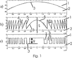
3 境界層
4,5 格子の側壁面
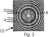
6 中心の放物面
7 格子谷部
8 格子山部
9 格子の深さ
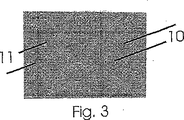
10,11 レンズ構造
Claims (12)
- 重ね合わされた少なくとも二つの材料層を有し、該少なくとも二つの材料層のうち少なくとも使用時に観察者に面する層は透明であり、前記二つの層間には、拡大レンズ的または縮小レンズ的効果を生じさせる光学的回折構造を有する境界面が少なくとも一部領域に形成されてなる転写フィルムまたはラミネートフィルムの層構造において、
前記レンズ的効果を生じさせる前記光学的回折構造(4,5,6;7,8)であるレンズ構造は、格子線密度およびその他の格子定数を含む格子構造が表面領域に亘って連続的に変えられて、2値構造(図1c)または、各格子谷部の一方の側壁面が、互いに平行でかつ前記境界面(3)の主面に対する垂線(S)にほぼ平行であり、かつ各格子谷部の他方の側壁面(4)の、前記境界面(3)の主面の垂線(S)に対する角度(α)が、前記レンズ構造の領域に亘ってほぼ連続的に変化するものである類似の構造(図1b)を形成するように設計され、前記レンズ構造の格子の深さ(9)が10μm以下であることおよび前記境界面(3)が、少なくとも一部の領域において、反射率を高める層を備えていることを特徴とする層構造。 - 前記境界面(3)に隣接する層(1,2)が透明であり、かつ屈折率差を有することを特徴とする請求項1記載の層構造。
- 前記屈折率差が0.2以上であることを特徴とする請求項2記載の層構造。
- 前記反射率を高める層が金属層であることを特徴とする請求項1記載の層構造。
- 多数のレンズ構造(10,11)が前記層構造の領域に分布していることを特徴とする請求項1から4のいずれか1項記載の層構造。
- 前記多数のレンズ構造(10,11)が網目状に配列されていることを特徴とする請求項5記載の層構造。
- ほぼ円形の前記レンズ構造(10)が同心的な格子線で形成されていることを特徴とする請求項1から6のいずれか1項記載の層構造。
- 前記レンズ構造(10)が、0.15mmから300mmまでの間の範囲の直径を有することを特徴とする請求項1から7のいずれか1項記載の層構造。
- 前記レンズ構造(10)が、3mmから50mmまでの間の範囲の直径を有することを特徴とする請求項8記載の層構造。
- 前記レンズ構造の回折格子の深さ(9)が5μm未満であることを特徴とする請求項1から9のいずれか1項記載の層構造。
- 前記レンズ構造の回折格子の深さ(9)が2μm未満であることを特徴とする請求項10記載の層構造。
- 前記2値構造(図1c)が前記レンズ構造(10)の全面に亘ってほぼ同じ深さ(9)を有することを特徴とする請求項1から11のいずれか1項記載の層構造。
Applications Claiming Priority (2)
| Application Number | Priority Date | Filing Date | Title |
|---|---|---|---|
| DE10254499A DE10254499B4 (de) | 2002-11-22 | 2002-11-22 | Schichtanordnung mit einer einen linsenartigen Effekt erzeugenden beugungsoptisch wirksamen Struktur |
| PCT/EP2003/012451 WO2004049250A1 (de) | 2002-11-22 | 2003-11-07 | Schichtanordnung mit einer einen linsenartigen effekt erzeugenden beugungsoptisch wirksamen struktur |
Publications (3)
| Publication Number | Publication Date |
|---|---|
| JP2006507526A JP2006507526A (ja) | 2006-03-02 |
| JP2006507526A5 JP2006507526A5 (ja) | 2009-03-12 |
| JP4510636B2 true JP4510636B2 (ja) | 2010-07-28 |
Family
ID=32318619
Family Applications (1)
| Application Number | Title | Priority Date | Filing Date |
|---|---|---|---|
| JP2004554325A Expired - Lifetime JP4510636B2 (ja) | 2002-11-22 | 2003-11-07 | レンズ的効果を生じさせる光学的回折構造を備えた層構造 |
Country Status (14)
| Country | Link |
|---|---|
| US (1) | US7227690B2 (ja) |
| EP (1) | EP1570422B1 (ja) |
| JP (1) | JP4510636B2 (ja) |
| KR (1) | KR100974682B1 (ja) |
| CN (1) | CN100419789C (ja) |
| AT (1) | ATE362627T1 (ja) |
| AU (1) | AU2003283371B2 (ja) |
| DE (2) | DE10254499B4 (ja) |
| ES (1) | ES2287538T3 (ja) |
| MY (1) | MY138939A (ja) |
| PL (1) | PL375554A1 (ja) |
| RU (1) | RU2317574C2 (ja) |
| TW (1) | TWI306514B (ja) |
| WO (1) | WO2004049250A1 (ja) |
Families Citing this family (23)
| Publication number | Priority date | Publication date | Assignee | Title |
|---|---|---|---|---|
| DE10254500B4 (de) * | 2002-11-22 | 2006-03-16 | Ovd Kinegram Ag | Optisch variables Element und dessen Verwendung |
| US7251398B2 (en) * | 2004-08-26 | 2007-07-31 | Interuniversitair Microelektronica Centrum (Imec) | Method for providing an optical interface and devices according to such methods |
| DE102004044459B4 (de) * | 2004-09-15 | 2009-07-09 | Ovd Kinegram Ag | Sicherheitsdokument mit transparenten Fenstern |
| DE102005017170B4 (de) | 2005-04-13 | 2010-07-01 | Ovd Kinegram Ag | Transferfolie, Verfahren zu deren Herstellung sowie Mehrschichtkörper und dessen Verwendung |
| DE102005017169B4 (de) | 2005-04-13 | 2023-06-22 | Ovd Kinegram Ag | Transferfolie |
| DE102005027380B4 (de) | 2005-06-14 | 2009-04-30 | Ovd Kinegram Ag | Sicherheitsdokument |
| DE102005061749A1 (de) | 2005-12-21 | 2007-07-05 | Giesecke & Devrient Gmbh | Optisch variables Sicherheitselement und Verfahren zu seiner Herstellung |
| US7973990B2 (en) * | 2006-04-27 | 2011-07-05 | Ricoh Company, Ltd. | Optical scanning device, optical writing device, and image forming apparatus |
| US8133638B2 (en) * | 2006-05-30 | 2012-03-13 | Brady Worldwide, Inc. | All-polymer grating microstructure |
| TW200913238A (en) * | 2007-06-04 | 2009-03-16 | Sony Corp | Optical member, solid state imaging apparatus, and manufacturing method |
| ES2320520B1 (es) * | 2007-11-21 | 2010-03-04 | Joaquin Devesa Company | Procedimiento de obtencion de una lamina lenticular y lamina asi obtenida. |
| FR2959830B1 (fr) | 2010-05-07 | 2013-05-17 | Hologram Ind | Composant optique d'authentification et procede de fabrication dudit composant |
| DE102010019766A1 (de) | 2010-05-07 | 2011-11-10 | Giesecke & Devrient Gmbh | Verfahren zur Erzeugung einer Mikrostruktur auf einem Träger |
| DE102010025775A1 (de) * | 2010-07-01 | 2012-01-05 | Giesecke & Devrient Gmbh | Sicherheitselement sowie Wertdokument mit einem solchen Sicherheitselement |
| RU2430836C1 (ru) | 2010-07-29 | 2011-10-10 | Федеральное Государственное Унитарное Предприятие "Гознак" (Фгуп "Гознак") | Многослойный защитный элемент с переменным оптическим эффектом и защищенный от подделки документ |
| CN102981194B (zh) * | 2012-11-23 | 2015-04-01 | 中国科学院物理研究所 | 单片式光学元件以及单片式衍射光学元件的设计方法 |
| FR3000112B1 (fr) | 2012-12-20 | 2015-03-06 | Arjowiggins Security | Structure de securite. |
| DE102015100280A1 (de) * | 2015-01-09 | 2016-07-14 | Ovd Kinegram Ag | Verfahren zur Herstellung von Sicherheitselementen sowie Sicherheitselemente |
| GB2545387A (en) | 2015-07-24 | 2017-06-21 | De La Rue Int Ltd | Security device and method of manufacturing thereof |
| GB201513096D0 (en) | 2015-07-24 | 2015-09-09 | Rue De Int Ltd | Diffractive security device and method of manufacturing thereof |
| JP2018114696A (ja) | 2017-01-19 | 2018-07-26 | 凸版印刷株式会社 | 表示体 |
| UA127132C2 (uk) * | 2017-09-29 | 2023-05-10 | Сікпа Холдінг Са | Тонкий оптичний захисний елемент і спосіб його виготовлення |
| DE102018103236A1 (de) | 2018-02-14 | 2019-08-14 | Leonhard Kurz Stiftung & Co. Kg | Sicherheitselement und Verfahren zur Herstellung eines Sicherheitselements |
Family Cites Families (19)
| Publication number | Priority date | Publication date | Assignee | Title |
|---|---|---|---|---|
| CA1267173A (en) * | 1985-09-23 | 1990-03-27 | Thomas I. Bradshaw | Sheet containing contour-dependent directional image and method for forming the same |
| DE3687560D1 (de) * | 1985-10-15 | 1993-03-04 | Gao Ges Automation Org | Datentraeger mit einem optischen echtheitsmerkmal sowie verfahren zur herstellung und pruefung des datentraegers. |
| GB9309673D0 (en) * | 1993-05-11 | 1993-06-23 | De La Rue Holographics Ltd | Security device |
| CN1063552C (zh) * | 1995-02-28 | 2001-03-21 | 中国科学技术大学 | 一种量子线超微细图形的制作方法 |
| JP3618465B2 (ja) * | 1996-05-31 | 2005-02-09 | オリンパス株式会社 | 回折光学素子、およびそれを用いる光学装置 |
| JP3618464B2 (ja) * | 1995-08-29 | 2005-02-09 | オリンパス株式会社 | 回折光学素子、およびそれを用いる光学装置 |
| DE69636991T2 (de) | 1995-11-28 | 2007-12-06 | Ovd Kinegram Ag | Optischer Informationsträger |
| JPH10116016A (ja) * | 1996-10-09 | 1998-05-06 | Dainippon Printing Co Ltd | 光回折パターン形成体 |
| AUPO289296A0 (en) * | 1996-10-10 | 1996-10-31 | Securency Pty Ltd | Self-verifying security documents |
| US5969864A (en) * | 1997-09-25 | 1999-10-19 | Raytheon Company | Variable surface relief kinoform optical element |
| JP3479449B2 (ja) * | 1998-02-04 | 2003-12-15 | 沖電気工業株式会社 | 反射型回折光学素子の製造方法 |
| US6324004B1 (en) * | 1999-01-21 | 2001-11-27 | Ovd Kingegram Ag | Planar patterns with superimposed diffraction gratings |
| DE59911557D1 (de) * | 1999-08-12 | 2005-03-10 | Ovd Kinegram Ag Zug | Datenträger |
| US6502757B1 (en) * | 1999-09-17 | 2003-01-07 | Dai Nippon Printing Co., Ltd. | Information recorded medium, device for reading the information, information recorded medium transfer foil, and method for producing information recorded medium |
| DE19949945A1 (de) * | 1999-10-16 | 2001-08-30 | Bundesdruckerei Gmbh | Datenträger mit Echtheitsmerkmalen und Herstellverfahren hierfür |
| JP2001332087A (ja) * | 2000-05-19 | 2001-11-30 | Nec Corp | センスアンプ回路 |
| JP3242638B2 (ja) * | 2000-07-07 | 2001-12-25 | キヤノン株式会社 | 表示素子および表示装置 |
| DE10054503B4 (de) * | 2000-11-03 | 2005-02-03 | Ovd Kinegram Ag | Lichtbeugende binäre Gitterstruktur und Sicherheitselement mit einer solchen Gitterstruktur |
| DE10123230A1 (de) * | 2001-05-12 | 2002-11-28 | Zeiss Carl | Diffraktives optisches Element sowie optische Anordnung mit einem diffraktiven optischen Element |
-
2002
- 2002-11-22 DE DE10254499A patent/DE10254499B4/de not_active Expired - Fee Related
-
2003
- 2003-11-07 ES ES03775318T patent/ES2287538T3/es not_active Expired - Lifetime
- 2003-11-07 AT AT03775318T patent/ATE362627T1/de active
- 2003-11-07 JP JP2004554325A patent/JP4510636B2/ja not_active Expired - Lifetime
- 2003-11-07 RU RU2005119642/28A patent/RU2317574C2/ru active
- 2003-11-07 US US10/535,732 patent/US7227690B2/en not_active Expired - Lifetime
- 2003-11-07 CN CNB2003801039085A patent/CN100419789C/zh not_active Expired - Fee Related
- 2003-11-07 EP EP03775318A patent/EP1570422B1/de not_active Expired - Lifetime
- 2003-11-07 WO PCT/EP2003/012451 patent/WO2004049250A1/de active IP Right Grant
- 2003-11-07 PL PL03375554A patent/PL375554A1/xx not_active Application Discontinuation
- 2003-11-07 AU AU2003283371A patent/AU2003283371B2/en not_active Ceased
- 2003-11-07 KR KR1020057009173A patent/KR100974682B1/ko active IP Right Grant
- 2003-11-07 DE DE50307303T patent/DE50307303D1/de not_active Expired - Lifetime
- 2003-11-12 TW TW092131640A patent/TWI306514B/zh not_active IP Right Cessation
- 2003-11-18 MY MYPI20034412A patent/MY138939A/en unknown
Also Published As
| Publication number | Publication date |
|---|---|
| RU2005119642A (ru) | 2006-01-27 |
| CN1714370A (zh) | 2005-12-28 |
| ES2287538T3 (es) | 2007-12-16 |
| PL375554A1 (en) | 2005-11-28 |
| CN100419789C (zh) | 2008-09-17 |
| JP2006507526A (ja) | 2006-03-02 |
| DE10254499B4 (de) | 2005-12-22 |
| US7227690B2 (en) | 2007-06-05 |
| TWI306514B (en) | 2009-02-21 |
| MY138939A (en) | 2009-08-28 |
| AU2003283371B2 (en) | 2008-04-03 |
| ATE362627T1 (de) | 2007-06-15 |
| DE50307303D1 (de) | 2007-06-28 |
| US20060072225A1 (en) | 2006-04-06 |
| EP1570422A1 (de) | 2005-09-07 |
| AU2003283371A1 (en) | 2004-06-18 |
| RU2317574C2 (ru) | 2008-02-20 |
| KR20050085086A (ko) | 2005-08-29 |
| TW200428019A (en) | 2004-12-16 |
| WO2004049250A1 (de) | 2004-06-10 |
| KR100974682B1 (ko) | 2010-08-06 |
| EP1570422B1 (de) | 2007-05-16 |
| DE10254499A1 (de) | 2004-06-17 |
Similar Documents
| Publication | Publication Date | Title |
|---|---|---|
| JP4510636B2 (ja) | レンズ的効果を生じさせる光学的回折構造を備えた層構造 | |
| JP4611747B2 (ja) | 光学可変素子およびその使用方法 | |
| JP2006507526A5 (ja) | ||
| JP2006507527A5 (ja) | ||
| JP5674781B2 (ja) | 多層体 | |
| JP6168411B2 (ja) | 多層体 | |
| US6043936A (en) | Diffractive structure on inclined facets | |
| JP4550054B2 (ja) | 光学的セキュリティ素子および隠された情報を可視化するためのシステム | |
| JP4983899B2 (ja) | 表示体及びラベル付き物品 | |
| JP2016505161A (ja) | 加飾エレメント及び加飾エレメントを備えるセキュリティドキュメント | |
| CN101952127A (zh) | 膜元件 | |
| JP2005525593A (ja) | 光学的可変素子 | |
| JP4876853B2 (ja) | Ovd媒体、およびovd媒体を備える情報印刷物 | |
| WO2018225801A1 (ja) | 光学構造体 | |
| JP5245430B2 (ja) | 表示体及びラベル付き物品 | |
| JP2013020084A (ja) | 計算機ホログラムを有する表示体及びラベル付き物品 | |
| CN113056376B (zh) | 光学可变元件、安全文件、用于制造光学可变元件的方法、用于制造安全文件的方法 | |
| EP2955564B1 (en) | Optically variable element | |
| KR101975925B1 (ko) | 입체이미지 패턴을 가진 필름 및 이의 제조방법 | |
| JP2021124602A (ja) | カラーシフトデバイス | |
| CN117460625A (zh) | 反射可见的光学安全部件、这种部件的制造以及配备有这种部件的安全文件 | |
| JP2022019238A (ja) | カラーシフトデバイス | |
| WO2019004463A1 (ja) | 光学構造体 |
Legal Events
| Date | Code | Title | Description |
|---|---|---|---|
| A131 | Notification of reasons for refusal |
Free format text: JAPANESE INTERMEDIATE CODE: A131 Effective date: 20080722 |
|
| A601 | Written request for extension of time |
Free format text: JAPANESE INTERMEDIATE CODE: A601 Effective date: 20081022 |
|
| A602 | Written permission of extension of time |
Free format text: JAPANESE INTERMEDIATE CODE: A602 Effective date: 20081029 |
|
| A524 | Written submission of copy of amendment under article 19 pct |
Free format text: JAPANESE INTERMEDIATE CODE: A524 Effective date: 20090122 |
|
| A131 | Notification of reasons for refusal |
Free format text: JAPANESE INTERMEDIATE CODE: A131 Effective date: 20090609 |
|
| A521 | Request for written amendment filed |
Free format text: JAPANESE INTERMEDIATE CODE: A523 Effective date: 20090909 |
|
| TRDD | Decision of grant or rejection written | ||
| A01 | Written decision to grant a patent or to grant a registration (utility model) |
Free format text: JAPANESE INTERMEDIATE CODE: A01 Effective date: 20100330 |
|
| A01 | Written decision to grant a patent or to grant a registration (utility model) |
Free format text: JAPANESE INTERMEDIATE CODE: A01 |
|
| A61 | First payment of annual fees (during grant procedure) |
Free format text: JAPANESE INTERMEDIATE CODE: A61 Effective date: 20100430 |
|
| FPAY | Renewal fee payment (event date is renewal date of database) |
Free format text: PAYMENT UNTIL: 20130514 Year of fee payment: 3 |
|
| R150 | Certificate of patent or registration of utility model |
Free format text: JAPANESE INTERMEDIATE CODE: R150 Ref document number: 4510636 Country of ref document: JP Free format text: JAPANESE INTERMEDIATE CODE: R150 |
|
| R250 | Receipt of annual fees |
Free format text: JAPANESE INTERMEDIATE CODE: R250 |
|
| R250 | Receipt of annual fees |
Free format text: JAPANESE INTERMEDIATE CODE: R250 |
|
| R250 | Receipt of annual fees |
Free format text: JAPANESE INTERMEDIATE CODE: R250 |
|
| R250 | Receipt of annual fees |
Free format text: JAPANESE INTERMEDIATE CODE: R250 |
|
| R250 | Receipt of annual fees |
Free format text: JAPANESE INTERMEDIATE CODE: R250 |
|
| R250 | Receipt of annual fees |
Free format text: JAPANESE INTERMEDIATE CODE: R250 |
|
| R250 | Receipt of annual fees |
Free format text: JAPANESE INTERMEDIATE CODE: R250 |
|
| R250 | Receipt of annual fees |
Free format text: JAPANESE INTERMEDIATE CODE: R250 |
|
| R250 | Receipt of annual fees |
Free format text: JAPANESE INTERMEDIATE CODE: R250 |
|
| R250 | Receipt of annual fees |
Free format text: JAPANESE INTERMEDIATE CODE: R250 |
|
| R250 | Receipt of annual fees |
Free format text: JAPANESE INTERMEDIATE CODE: R250 |
|
| EXPY | Cancellation because of completion of term |