JP4510636B2 - Layered structure with an optical diffractive structure producing a lens effect - Google Patents
Layered structure with an optical diffractive structure producing a lens effect Download PDFInfo
- Publication number
- JP4510636B2 JP4510636B2 JP2004554325A JP2004554325A JP4510636B2 JP 4510636 B2 JP4510636 B2 JP 4510636B2 JP 2004554325 A JP2004554325 A JP 2004554325A JP 2004554325 A JP2004554325 A JP 2004554325A JP 4510636 B2 JP4510636 B2 JP 4510636B2
- Authority
- JP
- Japan
- Prior art keywords
- lens
- layer
- layer structure
- structure according
- lattice
- Prior art date
- Legal status (The legal status is an assumption and is not a legal conclusion. Google has not performed a legal analysis and makes no representation as to the accuracy of the status listed.)
- Expired - Lifetime
Links
- 230000000694 effects Effects 0.000 title claims abstract description 32
- 230000003287 optical effect Effects 0.000 title claims description 15
- 239000000463 material Substances 0.000 claims description 13
- 239000002184 metal Substances 0.000 claims description 8
- 230000009467 reduction Effects 0.000 claims description 2
- 239000005001 laminate film Substances 0.000 claims 1
- 229920003002 synthetic resin Polymers 0.000 abstract description 2
- 239000000057 synthetic resin Substances 0.000 abstract description 2
- 239000010410 layer Substances 0.000 description 72
- 239000010408 film Substances 0.000 description 18
- 238000000034 method Methods 0.000 description 17
- 230000008901 benefit Effects 0.000 description 9
- 239000011248 coating agent Substances 0.000 description 7
- 238000000576 coating method Methods 0.000 description 7
- 239000004922 lacquer Substances 0.000 description 5
- 230000008859 change Effects 0.000 description 4
- 238000004519 manufacturing process Methods 0.000 description 4
- 239000000758 substrate Substances 0.000 description 4
- 239000004065 semiconductor Substances 0.000 description 3
- 239000010409 thin film Substances 0.000 description 3
- 230000000007 visual effect Effects 0.000 description 3
- 239000012790 adhesive layer Substances 0.000 description 2
- 239000003570 air Substances 0.000 description 2
- 230000005540 biological transmission Effects 0.000 description 2
- 238000010894 electron beam technology Methods 0.000 description 2
- 238000005516 engineering process Methods 0.000 description 2
- 238000005530 etching Methods 0.000 description 2
- 229920002120 photoresistant polymer Polymers 0.000 description 2
- 239000012080 ambient air Substances 0.000 description 1
- 230000003466 anti-cipated effect Effects 0.000 description 1
- 230000015572 biosynthetic process Effects 0.000 description 1
- 238000012790 confirmation Methods 0.000 description 1
- 239000000203 mixture Substances 0.000 description 1
- 230000001151 other effect Effects 0.000 description 1
- 230000002093 peripheral effect Effects 0.000 description 1
- 239000000049 pigment Substances 0.000 description 1
- 230000008569 process Effects 0.000 description 1
- 230000035484 reaction time Effects 0.000 description 1
- 238000002310 reflectometry Methods 0.000 description 1
- 230000035945 sensitivity Effects 0.000 description 1
- 238000001771 vacuum deposition Methods 0.000 description 1
- 238000000489 vacuum metal deposition Methods 0.000 description 1
Images
Classifications
-
- B—PERFORMING OPERATIONS; TRANSPORTING
- B42—BOOKBINDING; ALBUMS; FILES; SPECIAL PRINTED MATTER
- B42D—BOOKS; BOOK COVERS; LOOSE LEAVES; PRINTED MATTER CHARACTERISED BY IDENTIFICATION OR SECURITY FEATURES; PRINTED MATTER OF SPECIAL FORMAT OR STYLE NOT OTHERWISE PROVIDED FOR; DEVICES FOR USE THEREWITH AND NOT OTHERWISE PROVIDED FOR; MOVABLE-STRIP WRITING OR READING APPARATUS
- B42D25/00—Information-bearing cards or sheet-like structures characterised by identification or security features; Manufacture thereof
- B42D25/40—Manufacture
- B42D25/45—Associating two or more layers
- B42D25/465—Associating two or more layers using chemicals or adhesives
-
- G—PHYSICS
- G02—OPTICS
- G02B—OPTICAL ELEMENTS, SYSTEMS OR APPARATUS
- G02B5/00—Optical elements other than lenses
- G02B5/18—Diffraction gratings
-
- B—PERFORMING OPERATIONS; TRANSPORTING
- B42—BOOKBINDING; ALBUMS; FILES; SPECIAL PRINTED MATTER
- B42D—BOOKS; BOOK COVERS; LOOSE LEAVES; PRINTED MATTER CHARACTERISED BY IDENTIFICATION OR SECURITY FEATURES; PRINTED MATTER OF SPECIAL FORMAT OR STYLE NOT OTHERWISE PROVIDED FOR; DEVICES FOR USE THEREWITH AND NOT OTHERWISE PROVIDED FOR; MOVABLE-STRIP WRITING OR READING APPARATUS
- B42D25/00—Information-bearing cards or sheet-like structures characterised by identification or security features; Manufacture thereof
- B42D25/20—Information-bearing cards or sheet-like structures characterised by identification or security features; Manufacture thereof characterised by a particular use or purpose
- B42D25/29—Securities; Bank notes
-
- B—PERFORMING OPERATIONS; TRANSPORTING
- B42—BOOKBINDING; ALBUMS; FILES; SPECIAL PRINTED MATTER
- B42D—BOOKS; BOOK COVERS; LOOSE LEAVES; PRINTED MATTER CHARACTERISED BY IDENTIFICATION OR SECURITY FEATURES; PRINTED MATTER OF SPECIAL FORMAT OR STYLE NOT OTHERWISE PROVIDED FOR; DEVICES FOR USE THEREWITH AND NOT OTHERWISE PROVIDED FOR; MOVABLE-STRIP WRITING OR READING APPARATUS
- B42D25/00—Information-bearing cards or sheet-like structures characterised by identification or security features; Manufacture thereof
- B42D25/30—Identification or security features, e.g. for preventing forgery
- B42D25/305—Associated digital information
-
- B—PERFORMING OPERATIONS; TRANSPORTING
- B44—DECORATIVE ARTS
- B44C—PRODUCING DECORATIVE EFFECTS; MOSAICS; TARSIA WORK; PAPERHANGING
- B44C3/00—Processes, not specifically provided for elsewhere, for producing ornamental structures
- B44C3/02—Superimposing layers
-
- B—PERFORMING OPERATIONS; TRANSPORTING
- B44—DECORATIVE ARTS
- B44F—SPECIAL DESIGNS OR PICTURES
- B44F7/00—Designs imitating three-dimensional effects
-
- B—PERFORMING OPERATIONS; TRANSPORTING
- B42—BOOKBINDING; ALBUMS; FILES; SPECIAL PRINTED MATTER
- B42D—BOOKS; BOOK COVERS; LOOSE LEAVES; PRINTED MATTER CHARACTERISED BY IDENTIFICATION OR SECURITY FEATURES; PRINTED MATTER OF SPECIAL FORMAT OR STYLE NOT OTHERWISE PROVIDED FOR; DEVICES FOR USE THEREWITH AND NOT OTHERWISE PROVIDED FOR; MOVABLE-STRIP WRITING OR READING APPARATUS
- B42D25/00—Information-bearing cards or sheet-like structures characterised by identification or security features; Manufacture thereof
- B42D25/30—Identification or security features, e.g. for preventing forgery
- B42D25/324—Reliefs
Abstract
Description
本発明は、少なくとも二つの重ね合わされた材料層を有する、特に転写フィルムまたは貼付けフィルムに実施するための層構造に関し、これら材料層のうちの、使用時に少なくとも観察者に面する層が透明または半透明の外観を有し、層間には、少なくとも一部の領域において、拡大レンズまたは縮小レンズ的効果を生じさせる光学的回折構造を有するように形成された層構造に関するものである。 The present invention relates to a layer structure having at least two superimposed material layers, in particular for carrying out on transfer films or affixed films, in which at least the layer facing the viewer when used is transparent or semi-transparent. The present invention relates to a layer structure that has a transparent appearance and is formed so as to have an optical diffractive structure that causes a magnifying lens or reduction lens effect between layers at least in some regions.
これに関連して、上記転写フィルムは、ベースフィルムと、サブストレートに転写するためにベースフィルムから剥がされる転写層とからなる、特にいわゆるエンボスフィルムを含む。通常エンボスフィルムの転写層はラッカー層からなり、本発明では「材料層」という語は主としてラッカー層を意味し、或る場合は接着層の意味でもある。しかしながら、本発明は、「材料層」が、周囲の空気、または金属被膜、または誘電体被膜または半導体被膜によって形成される他の実施例も包含する。貼付けフィルムの構造は、合成樹脂層またはラッカー層がベースフィルムから剥がされずにベースフィルムとともにサブストレートに貼り付けることができることを除いては、転写フィルムの構造と実質的に一致する。この種の層構造を備えた転写フィルムおよびは貼付けフィルムは、装飾的用途にも用いられるが、特にセキュリティの用途に用いられる。 In this connection, the transfer film comprises in particular a so-called embossed film consisting of a base film and a transfer layer that is peeled off from the base film for transfer to a substrate. Usually, the transfer layer of the embossed film is composed of a lacquer layer. In the present invention, the term “material layer” mainly means a lacquer layer, and in some cases also means an adhesive layer. However, the present invention also encompasses other embodiments in which the “material layer” is formed by ambient air, or a metal coating, or a dielectric or semiconductor coating. The structure of the affixing film substantially matches that of the transfer film except that the synthetic resin layer or the lacquer layer can be affixed to the substrate together with the base film without being peeled off from the base film. A transfer film and a sticking film having this type of layer structure are also used for decorative purposes, but are particularly used for security purposes.
上述した形式の層構造は今や知られており、例えば一様な外観を備えたレンズの形態で用いられるようになって来ており、クレジットカード(Amex-Blue)におけるセキュリティ素子として新しく市場で用いられている。これらのクレジットカードにおいては、比較的大きい直径の領域に亘ってレンズ的効果が現れ、実質的に偏光レンズの形態を有する。公知の層構造の光学的回折構造によって生じるレンズ的効果においては、ホログラフィー技術によって形成された、一般に正弦波的表面輪郭を備えた構造が用いられている。このような技術的努力が比較的少ないホログラフィー技術により製造されたレンズは、レンズ効果を備えた光学的回折構造が円形または楕円形の平面形状を有するレンズが含まれる場合にのみ可能になるということ以外に、多くの欠点を有する。ホログラフィー技術により形成されたレンズの一つの欠点は、例えば極めて明るい外観は有さず、特に一般に中心領域では凹凸に見え、これによって、レンズが生じさせなければならない視覚的効果が相当に損なわれることである。ホログラフィー技術により形成されたレンズのさらなる欠点は、デザイン上の大きい自由度を備えた色彩効果を得ることが事実上不可能であることである。 Layer structures of the type described above are now known, for example in the form of lenses with a uniform appearance and are used in the new market as security elements in credit cards (Amex-Blue). It has been. In these credit cards, a lens effect appears over a relatively large diameter region and has a substantially polarizing lens configuration. In the lens effect caused by optical diffraction structure of known layer structure was formed by holographic techniques, it has been used commonly with a sinusoidally surface contour structures. Lenses manufactured by holographic techniques with relatively little technical effort are only possible if the optical diffractive structure with lens effect includes a lens with a circular or elliptical planar shape. Besides, it has many drawbacks. One disadvantage of lenses formed by holographic techniques is, for example, that they do not have a very bright appearance, especially in the central region, which appears uneven, which considerably impairs the visual effects that the lens must produce. It is. A further disadvantage of lenses formed by holographic techniques is that it is virtually impossible to obtain color effects with great design freedom.
本発明の目的は、ホログラフィー技術により形成された、正弦波的表面輪郭を備えた公知のレンズ構造が有する上述のような欠点を備えていない上述した種類の層構造を提供すること、すなわち、実施可能な技術を用いて、極めて精密にかつ種々の形態でレンズ的効果を与える構造を製造可能な方法で妥当な時間内に形成すること、その結果、ホログラフィー技術によって形成された構造によって生じる効果に比較してかなり改良されたレンズ的効果により、効果の効率および明るさを高め、最終的に、少なくとも色彩効果の生成において、ホログラフィー技術によって形成された構造によって可能になるよりもかなり大きい自由度を提供することにある。 The object of the present invention is to provide a layer structure of the kind described above which does not have the disadvantages mentioned above, which are known from the known lens structures with sinusoidal surface contours formed by holographic techniques. Using a possible technique, the structure that gives the lens effect in a very precise and different form is formed in a reasonable time in a manufacturable way, so that the effect produced by the structure formed by the holographic technique is reduced. The significantly improved lenticular effect compared to increases the efficiency and brightness of the effect, and ultimately gives a greater degree of freedom at least in the generation of color effects than is possible with the structure formed by holographic techniques. It is to provide.
本発明によれば、上記レンズ的効果を生じさせる光学的回折構造(以下「レンズ構造」と呼ぶ)は、格子線密度およびその他の随意的な格子定数を含む格子構造が表面領域に亘って連続的に変えられて、2値構造または、各格子谷部の一方の側壁面が、互いに平行でかつ境界層(境界面)の主面に対する垂線にほぼ平行であり、かつ各格子谷部の他方の側壁面の、境界層の主面に対する垂線に対する角度がレンズ構造の領域に亘ってほぼ連続的に変化するものである類似の構造を形成するように設計され、回折格子の深さ9は10μm以下である。 According to the present invention, the optical diffractive structure that produces the lens effect (hereinafter referred to as “lens structure”) has a continuous lattice structure including a lattice line density and other optional lattice constants over the surface region. The one side wall surface of each lattice valley portion is parallel to each other and substantially parallel to the perpendicular to the main surface of the boundary layer (boundary surface) , and the other of each lattice valley portion Are designed to form a similar structure in which the angle of the side wall surface to the normal to the principal surface of the boundary layer varies substantially continuously over the region of the lens structure, and the grating depth 9 is 10 μm. It is as follows.
本明細書における「2値構造」とは、格子谷部および格子山部がほぼ長方形の断面形状を有する構造を意味し、レンズ効果を生じさせるためには、レンズの中心から周縁に向かって格子定数が連続的に変化しなければならないが、一般的な意味では、2値格子において谷部の幅と山部の幅との双方が連続的に変化することになる。充分に微細な2値格子は、適当なマスクを使用することによって容易に生成させることができ、これによって、より高い正確性のみでなく、製造コストを比較的低く抑えることができる。 The “binary structure” in this specification means a structure in which the lattice valley portion and the lattice mountain portion have a substantially rectangular cross-sectional shape, and in order to produce a lens effect, the lattice is directed from the center of the lens toward the periphery. The constant must change continuously, but in a general sense, both the width of the valley and the width of the peak will change continuously in the binary lattice. A sufficiently fine binary grid can be easily generated by using an appropriate mask, which not only provides higher accuracy, but can also keep manufacturing costs relatively low.
請求項に記載された格子構造の他の実施の形態は、レーザービームまたは電子ビーム蝕刻プリンタを利用した、いわゆる「直接書込み」法によって作成されるのが好ましい。これらの方法を用いた場合、特に請求項に記載されているような、各格子谷部の一方の側壁面がレンズ形成格子の主面に対する垂線にほぼ平行であり、かつ各格子谷部の他方の側壁面が傾斜して、格子のベースに向かって先細になっている、極めて精密な格子構造を作成することが容易になる。これと関連して、連続的な輪郭ではなく、むしろほぼ階段状に配列された傾斜壁面を形成することも可能であり、多くの用途に対しては4段または8段で充分である。しかしながら、高い品質が求められるときには、例えば64段とすることも可能である。 Another embodiment of the claimed grating structure is preferably produced by a so-called “direct writing” method using a laser beam or electron beam etching printer. When these methods are used, one side wall surface of each lattice valley is substantially parallel to a perpendicular to the main surface of the lens-forming lattice, and the other of each lattice valley as described in the claims. It is easy to create a very precise lattice structure in which the side wall surface of the surface is inclined and tapered toward the base of the lattice. In this connection, it is also possible to form inclined wall surfaces arranged in a substantially stepped manner rather than a continuous contour, and for many applications four or eight steps are sufficient. However, when high quality is required, for example, 64 stages can be used.
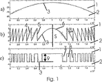
このような格子の構成に関し、単純化のために図1を参照すると、図1aは通常の回折レンズの断面図を示し、中間の図1bは、各格子谷部の一方の側壁面が格子の主面に対し垂直に延び、対向壁面が傾斜している回折レンズの断面を概略的に示している。図1cには、いわゆる「2値構造」が示され、格子谷部および格子山部の双方が長方形の断面形状を有し、図1cから明らかなように、格子山部の幅および格子谷部の幅がレンズの中心から周縁に向かって減少している。図1に示された3種類のレンズはすべて、基本的には、いかなる特定の波長に対しても同様の光学的効果を生じさせる。 With regard to the structure of such a grating, referring to FIG. 1 for simplicity, FIG. 1a shows a cross-sectional view of a normal diffractive lens, and FIG. 1b in the middle shows that one side wall surface of each grating valley is a grating. 1 schematically shows a cross section of a diffractive lens extending perpendicularly to a main surface and having an inclined opposing wall surface. FIG. 1 c shows a so-called “binary structure”, where both the lattice valleys and the lattice peaks have a rectangular cross-sectional shape, and as is clear from FIG. 1 c, the width of the lattice peaks and the lattice valleys Is reduced from the center of the lens toward the periphery. All three types of lenses shown in FIG. 1 basically produce a similar optical effect for any particular wavelength.
しかしながら、本発明で提案された回折レンズ構造は、屈折レンズとは異なり、存在する光の波長に応じて異なる視覚的印象を呈する。それにも拘わらず、図1bおよび図1cに示された構成を有する回折レンズの高さは、図1aに描かれた対応する回折レンズの厚さの数分の一である。すべての実際の目的に関し層厚さに手を加えることなしには不可能と考えられていた、レンズ構造を層構造に組み込むことがこの方法によって初めて可能になった。 However, unlike the refractive lens, the diffractive lens structure proposed in the present invention presents a different visual impression depending on the wavelength of light present. Nevertheless, the height of a diffractive lens having the configuration shown in FIGS. 1b and 1c is a fraction of the thickness of the corresponding diffractive lens depicted in FIG. 1a. This method made it possible for the first time to incorporate a lens structure into a layer structure , which was considered impossible without altering the layer thickness for all practical purposes.
本発明によるレンズ構造が使用される場合、得られる第1の利益は、ホログラフィー技術で製造されたレンズによって得られるよりも高い効率が得られることであり、このことは、レンズの助けを借りて作成される画像、装飾的効果またはセキュリティ効果がより明るいことを意味する。他の利益は、本発明によるレンズ構造が、ホログラフィー技術で製造された構造と比較して極めて高い正確性をもって作成することができることであり、これによって、視覚的外観が著しく改善される。最後の利益は、本発明の構造をもってすれば、格子定数(格子密度、谷部の深さ等)を適切に選択することによって、レンズ構造の全体の輪郭に亘って、特殊の色彩効果を得ること、またはこの色彩効果を所定の態様で制御することができることである。さらに、これに関連して、このレンズ構造を、例えば、動的効果、反転または類似の効果を得るための光学的効果を生じさせる他の素子と組み合わせること、あるいは、例えば光学的に変化するセキュリティ素子によって一般に知られているような、特殊の色彩効果を生じさせるための薄膜構造と組み合わせることの可能性も考慮すべきである。したがって、本発明のレンズ構造は、ホログラフィー技術で製造された構造と比較して、「厚さ」が薄いという共通点に加えて多くの利点を有する。 When the lens structure according to the invention is used, the first benefit obtained is that it is more efficient than that obtained with a lens manufactured with holographic technology, which with the help of the lens It means that the image created, decorative effect or security effect is brighter. Another benefit is that the lens structure according to the invention can be made with very high accuracy compared to structures manufactured with holographic technology, which significantly improves the visual appearance. The last benefit is that with the structure of the present invention, a special color effect is obtained over the entire contour of the lens structure by appropriately selecting the lattice constant (grating density, valley depth, etc.). Or that this color effect can be controlled in a predetermined manner. Furthermore, in this connection, the lens structure can be combined with other elements that produce optical effects, for example dynamic effects, inversions or similar effects, or for example optically changing security. Consideration should also be given to the possibility of combining with thin film structures for producing special color effects, as is generally known by the device. Thus, the lens structure of the present invention has many advantages in addition to the common “thickness” compared to the structure produced by holographic techniques.
本発明によるレンズ構造を備えた層構造は、反射のみでなく透過の観点からも特殊な光学的効果を生じさせることができる。透過光で観察することを可能にするために、本発明は、透明でかつ屈折率が顕著に異なる、好ましくは少なくとも0.2は異なる、境界層に隣接する複数の層を提供する。屈折率の差は、境界面に作用して、光が層構造を通過するという事実にも拘わらず、はっきりと見える光学的効果を生じさせる。透過に対し作用する特別な特徴は、格子の一方側を覆う必要がなく、その代わりに空気に曝すことができることである。 The layer structure provided with the lens structure according to the present invention can produce a special optical effect from the viewpoint of transmission as well as reflection. In order to be able to observe with transmitted light, the present invention provides a plurality of layers adjacent to the boundary layer that are transparent and have significantly different refractive indices, preferably at least 0.2 different. The difference in refractive index acts on the interface and produces an optical effect that is clearly visible despite the fact that light passes through the layer structure . A special feature that acts on permeation is that it does not need to cover one side of the grid, but instead can be exposed to air.
さらに上記境界面が、少なくともその一部領域に亘って、金属層からなる都合の良い反射率増大層を例えば真空蒸着によって備えることも本発明の範囲内である。しかしながら、適当に高い屈折率を備えた透明な反射率増大層を考慮することも勿論考えられ、その場合、層構造は或る程度透明に形成することができる。公知の層組合せからなる薄膜構造または半導体層も用いることができる。 Further, it is within the scope of the present invention that the boundary surface is provided with a convenient reflectance increasing layer made of a metal layer, for example, by vacuum deposition over at least a partial region thereof. However, it is of course also conceivable to consider a transparent reflectivity increasing layer with a suitably high refractive index, in which case the layer structure can be made somewhat transparent. Thin film structures or semiconductor layers made of known layer combinations can also be used.
ありきたりの層構造を利用して作成される、公知のクレジットカードにおけるホログラフィー技術で形成されたセキュリティ素子は、単一の偏光レンズ構造のみを備えている。一方、本発明の回折レンズ構造を用いると、層構造の表面全体に亘って複数のレンズ構造を配置することができ、これによって、より興味深い効果(装飾的用途に関して)を得ることができ、あるいは、このレンズ構造がセキュリティ素子の一部である場合に、増大されたセキュリティ効果を得ることができる。後者の場合、確認を容易にするために、多数のレンズを網目状に配置することができる。あるいは、複数のレンズ構造が少なくとも一部において重なり合った構造も考えられ、その場合には、異なるレンズ構造が異なる観察角度で現れるように入れ子にしてもよい。 A security element formed by a holographic technique in a known credit card, which is created using a conventional layer structure , comprises only a single polarizing lens structure. On the other hand, with the diffractive lens structure of the present invention, a plurality of lens structures can be arranged over the entire surface of the layer structure , thereby obtaining a more interesting effect (for decorative applications), or An increased security effect can be obtained when this lens structure is part of the security element. In the latter case, a large number of lenses can be arranged in a mesh shape for easy confirmation. Alternatively, a structure in which a plurality of lens structures are at least partially overlapped is conceivable. In this case, different lens structures may be nested so that they appear at different observation angles.
もし本発明によって提案されたように、レンズ構造が同心的格子線の形態を採る実質的に環状であれば、このようなレンズ構造またはレンズ構造配列の製造は特に容易である。 Manufacturing of such a lens structure or lens structure arrangement is particularly easy if the lens structure is substantially annular, as proposed by the present invention, in the form of concentric grating lines.
実際に、もしレンズ構造の直径が、0.15mmと300mmとの間、好ましくは3mmと50mmとの間であれば便利であることが判明している。 In fact, it has proven convenient if the diameter of the lens structure is between 0.15 mm and 300 mm, preferably between 3 mm and 50 mm.
もし、本発明によって提供されたように、レンズ構造の格子の深さが5μm未満であれば、好ましくは3μm未満であれば、このような格子構造は、転写フィルムまたは貼付けフィルムの、ほぼこの厚さを有するラッカー層内に容易に組み込むことができる。 If the depth of the grating of the lens structure is less than 5 μm, preferably less than 3 μm, as provided by the present invention, such a grating structure is approximately the thickness of the transfer film or affixed film. It can be easily incorporated into a lacquer layer having a thickness.
本発明によれば、上記2値構造はレンズ構造の全表面に亘ってほぼ同じ深さを有する。これにより製造が著しく容易になる。この2値構造の深さの選択はレンズ構造を注目する観察者によって知覚される色彩に影響を与える。 According to the invention, the binary structure has substantially the same depth over the entire surface of the lens structure. This greatly facilitates production. The choice of the depth of this binary structure affects the color perceived by an observer who focuses on the lens structure.
最後に、もし観察者(単数または複数)が眺める透明層(単数または複数)が顔料を使用しないで着色されていれば、それが利点になり得る。 Finally, it can be an advantage if the transparent layer (s) viewed by the viewer (s) are colored without the use of pigments .
本発明のさらなる特徴、詳細および利点は、図面を参照して後述する好ましい実施の形態の説明から明らかになるであろう。 Further features, details and advantages of the present invention will become apparent from the description of preferred embodiments which follows with reference to the drawings.
図1の概略的断面図において、二つの材料層1および2を備えた、本発明による層構造が示されており、これら二つの材料層1および2間には、例えば真空金属蒸着によって金属被膜を付され得る境界層3が設けられている。用途によっては、材料層1および2は空気で形成しても差支えない。レンズ構造の正確なサイズおよび正確な直径は問題にならないので、図1におけるレンズの直径は、X軸に沿った無名数で特定されている。しかしながら、このレンズ構造の直径は、一般的に0.5mmと300mmとの間、好ましくは3mmと50mmとの間にあり、焦点距離は通常、レンズの直径に等しい値とこの値の5倍との間にある。
In the schematic cross-sectional view of FIG. 1, a layer structure according to the invention with two
図1のY軸上には、材料層1,2の厚さすなわちレンズ構造の高さが、位相差をラジアンで表す値で目盛られている。特定の波長(例えば肉眼に対し最大の感度を有する550nm)の光を用いることによって、この位相差から公知の方法(対応する屈折率を計算することを含む)で幾何学的深さを計算することができる。図1aを図1bおよび図1cと比較すると、図1aに表されている層構造の厚さは、図1bに表されている層構造の厚さの少なくとも10倍でなければならず、図1cに表されている層構造の厚さの約20倍でなければならないことが明らかである。図1bおよび図1cの層構造が図1aの層構造よりも実質的に薄くすることができるということは、高さをカバーする境界層3に基づくレンズ構造の全体の低い高さ9と関係し、この高さは、図1bについて(透過におけるn=1.5/n=1の系について)計算すると波長のほぼ2倍に過ぎず、図1cについて計算すると波長にほぼ等しい。
On the Y-axis of FIG. 1, the thicknesses of the
層構造の層1および2は、一般に適当な組成を有するラッカー層であり、少なくとも観察者に面した層(この場合は一般に層1)は、希望により着色されていてもよいが、実質的に透明である。用途によっては、一方の層が接着層であってもよく、観察者に面した層が省かれていてもよい。
もし境界層3が金属被膜であったり、他の高反射性被膜を備えたりしている場合には、層2は同様に透明であったり、半透明または不透明であったりしてもよい。一方、もし本発明による層構造が、例えばサブストレート上に実在する可視特徴物の覆いとして光を透過する用途に用いられる場合には、層2も透明でなければならない。この場合、境界層3は、一般に不透明な金属被膜であってはならない。二つの透明層1および2は、それらの屈折率が異なる(屈折率の差は少なくとも0.2)ように選択されなければならず、その結果、二つの透明層1および2を用いているにも拘わらず、境界層3によって生成される効果を光学的に明白に視ることができる。
If the
図1bに表されているレンズ構造は、「直接書込み法」により、すなわちレーザーを用いたアブレーションによって材料が所望の輪郭に一致するように造形されることにより、あるいは、レーザーまたは電子ビーム蝕刻プリンタを用いて所望の輪郭にパターン化されたホトレジストを露光し、次いでホトレジストの現像によって所望の輪郭または陰画を得ることによって生成される。この処理には、種々の異なる回折格子構造を作成することができるという利益があり、特に、例えば用途によってはいわゆるブレーズ格子のような種々の異なる回折格子断面形状を提供することができる。垂直面Sに対し平行に延びる格子谷部の側壁面5が、境界層3の中央の楕円状部分のみでなく、格子谷部の斜面4によって形成された準不連続性部分を、どちらかというと実質的に平滑なレンズ輪郭内に形成するという事実を考慮すると、図1bに明らかに示されているように、格子谷部の斜面4とレンズ構造の主面に垂直な面Sとの間の角度αを、レンズの中心から周縁部まで連続的に変えることができるという事実は特に注目すべきである。
The lens structure shown in FIG. 1b can be produced by “direct writing”, that is, by ablating with a laser, the material being shaped to match the desired contour, or by using a laser or electron beam etching printer. Used to expose the photoresist patterned to the desired contour and then develop the photoresist to obtain the desired contour or negative. This process has the advantage that a variety of different diffraction grating structures can be created, in particular, depending on the application, it can provide a variety of different diffraction grating cross-sectional shapes such as so-called blaze gratings. The side wall surface 5 of the lattice valley portion extending parallel to the vertical plane S is not only the central elliptical portion of the
このようなレンズ構造は、これらを計算する方法とともに、文献に基本的に記載されているから、ここではそれ以上は言及しない。 Such lens structures are basically described in the literature, together with the methods for calculating them, so no further mention is made here.
図1bに示されているような高さ9方向に延びる連続的な斜めの側壁面4に代えて、斜めの側壁面4によって提供される光学的効果にほぼ等しい効果を有する階段を表面に備えた階段状構造を用いる可能性について言及すると、このような格子構造は、いわゆる直接書込み法を用いて、あるいは適当なマスク技法を用いて形成することができ、段の数は求める結果に応じて変る。多くの用途に関して、4段または8段に分割されていれば充分である。より高い品質が要求される場合には、例えば64段すなわち8段の二乗に等しい段数を備えることが可能である。
Instead of a continuous oblique
図1cに表されている2値構造は、適当なマスクの使用によって形成することができる。図1cに示されているような2値構造の本質的な特徴は、格子谷部7と格子の山部8との双方が本質的に長方形の断面を有するという事実にある。図1cに示されている構造の別の固有の特徴は、格子の深さ9がレンズ構造全体に亘って一定であり、このことは、特に製造に関して利益を提供するもので、材料除去媒体について反応時間を異ならせる必要もなければ、マスクを通過してサブストレートに作用する材料除去媒体を異なる強さをもって作用させる必要もない。 The binary structure represented in FIG. 1c can be formed by the use of a suitable mask. An essential feature of the binary structure as shown in FIG. 1c lies in the fact that both the lattice valleys 7 and the lattice peaks 8 have an essentially rectangular cross section. Another inherent feature of the structure shown in FIG. 1c is that the grating depth 9 is constant over the entire lens structure, which provides benefits especially in terms of manufacturing, for material removal media There is no need for different reaction times, and there is no need for the material removal medium acting on the substrate through the mask to have different strengths.
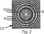
図2は、図1bに示されたのと同様のレンズ構造を備えて製造されたレンズ状素子の概略図であり(実際には格子線の間隔はもっと狭い)、図2の平面図は、偏光レンズの中心から周縁に向かって、個々の格子の山部間の間隔が一定の割合で狭まり、かつ格子密度が一定の割合で増大することを明らかに示している。それに加えて、図2の平面図に見られる格子側壁面4の傾斜が、レンズの中心から周縁部に向かって、一定の割合でかつ連続的な態様で変化していることを見ることができる。図2においては、レンズの主面に垂直な格子側壁面5を暗い線として明らかに見ることができる。
FIG. 2 is a schematic view of a lenticular element manufactured with a lens structure similar to that shown in FIG. 1b (actually the grid line spacing is narrower), and the plan view of FIG. It clearly shows that the distance between the peak portions of the individual gratings narrows at a constant rate and the lattice density increases at a constant rate from the center of the polarizing lens to the periphery. In addition, it can be seen that the inclination of the grating
図3は、本発明による層構造を意図した回折レンズ構造のさらなる可能性を示す図である。 FIG. 3 shows a further possibility of a diffractive lens structure intended for a layer structure according to the invention.
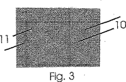
図3に示された実施の形態は、例えば装飾用の転写フィルムまたは貼付けフィルムに実施可能なものであり、理論的には図2のレンズ構造と同じ格子パターンを有する多数の偏光レンズ構造がフィルムの表面の複数の領域に分布している。この構造では、外側の格子谷部が、図2に見られる外側の一部の谷部の場合のように省略されてはいない。それとは反対に、図3のレンズ構造10はすべて円を描いている。図3の層構造において複数の偏光レンズ構造の外接によって偏光レンズ構造間に生じた、特有の形状の回折構造11を備えた球面四辺形状のスペースは、もし所望であれば、レンズ構造10が例えば収束レンズとしての機能を有するのに対し、レンズ構造11が拡散レンズとして機能するようにレンズ効果をも生じさせることもでき、これによって双方のレンズ形式の光学的効果があたかも強められたようになる。
The embodiment shown in FIG. 3 can be applied to, for example, a decorative transfer film or a pasting film, and a number of polarizing lens structures having the same lattice pattern as the lens structure of FIG. It is distributed over several areas of the surface. In this structure, the outer lattice valleys are not omitted as in the case of some of the outer valleys seen in FIG. On the other hand, the
異なるレンズ構造を適切に組み合わせることによって、複雑な光学的効果を示す層構造を生じさせることが可能なことは明らかであり、例えば動的効果、反転等の完全に異なる種類の効果を生じるその他の局部的に異なる回折構造を設計することも可能である。また、複数のレンズ構造および/または他の複数の回折構造を、例えばOVIのような特別の色彩を有する一連の薄いフィルムと組み合わせたり、特別の色彩変化を得るために、半導体層と組み合わせたりすることも考えられる。 Obviously, the proper combination of different lens structures can produce layer structures that exhibit complex optical effects, such as dynamic effects, other effects that produce completely different types of effects such as inversion. It is also possible to design locally different diffractive structures. Also, multiple lens structures and / or other multiple diffractive structures may be combined with a series of thin films having a special color, such as OVI, or combined with a semiconductor layer to obtain a special color change. It is also possible.
層構造の特に興味深い実施の形態は、境界層3の一部のみに金属被膜が付されている場合である。例えば、レンズ構造と見当を合わせた金属被膜除去も実行可能である。
A particularly interesting embodiment of the layer structure is when only a part of the
さらに、レンズ構造は、一般に図に示されているような円形とは限らない。回折レンズ構造を用いることによって得られる利益は、例えば三次元的外観を有する形成物を得るために、他の形態(いわゆる自由形状表面)を重ね合わせることができることである。さらに、例えば図2のレンズ構造を部品に分割して、これら部品を異なる方法で一体にすると極めて興味深い光学的効果が再び得られるであろうことも予想される。 Furthermore, the lens structure is not always circular as shown in the figure. The benefit obtained by using a diffractive lens structure is that other forms (so-called freeform surfaces) can be superimposed, for example, to obtain a formation having a three-dimensional appearance. It is further anticipated that, for example, dividing the lens structure of FIG. 2 into parts and bringing these parts together in different ways will again yield very interesting optical effects.
1,2 材料層
3 境界層
4,5 格子の側壁面
6 中心の放物面
7 格子谷部
8 格子山部
9 格子の深さ
10,11 レンズ構造
DESCRIPTION OF
Claims (12)
前記レンズ的効果を生じさせる前記光学的回折構造(4,5,6;7,8)であるレンズ構造は、格子線密度およびその他の格子定数を含む格子構造が表面領域に亘って連続的に変えられて、2値構造(図1c)または、各格子谷部の一方の側壁面が、互いに平行でかつ前記境界面(3)の主面に対する垂線(S)にほぼ平行であり、かつ各格子谷部の他方の側壁面(4)の、前記境界面(3)の主面の垂線(S)に対する角度(α)が、前記レンズ構造の領域に亘ってほぼ連続的に変化するものである類似の構造(図1b)を形成するように設計され、前記レンズ構造の格子の深さ(9)が10μm以下であることおよび前記境界面(3)が、少なくとも一部の領域において、反射率を高める層を備えていることを特徴とする層構造。It has at least two material layers superimposed, and at least the layer facing the observer at the time of use of the at least two material layers is transparent, and a magnifying lens effect or a reduction lens effect is provided between the two layers. In a layer structure of a transfer film or a laminate film in which an interface having an optical diffractive structure to be formed is formed in at least a partial region,
The lens structure which is the optical diffractive structure (4, 5, 6; 7, 8) that produces the lens effect has a lattice structure including a lattice line density and other lattice constants continuously over the surface region. The binary structure (FIG. 1c), or one of the sidewall surfaces of each lattice valley is parallel to each other and substantially parallel to the normal (S) to the principal surface of the boundary surface (3), and The angle (α) of the other side wall surface (4) of the lattice valley portion with respect to the normal (S) of the main surface of the boundary surface (3) changes substantially continuously over the region of the lens structure. Designed to form some similar structure (FIG. 1b), the grating depth (9) of the lens structure is less than 10 μm and the interface (3) is reflective in at least some areas Layer structure characterized by comprising a layer for increasing the rate.
Applications Claiming Priority (2)
| Application Number | Priority Date | Filing Date | Title |
|---|---|---|---|
| DE10254499A DE10254499B4 (en) | 2002-11-22 | 2002-11-22 | Layer arrangement with a lens-like effect generating diffractive optical effective structure |
| PCT/EP2003/012451 WO2004049250A1 (en) | 2002-11-22 | 2003-11-07 | Layer arrangement provided with a structure producing a diffractive optical effect and a lens-type effect |
Publications (3)
| Publication Number | Publication Date |
|---|---|
| JP2006507526A JP2006507526A (en) | 2006-03-02 |
| JP2006507526A5 JP2006507526A5 (en) | 2009-03-12 |
| JP4510636B2 true JP4510636B2 (en) | 2010-07-28 |
Family
ID=32318619
Family Applications (1)
| Application Number | Title | Priority Date | Filing Date |
|---|---|---|---|
| JP2004554325A Expired - Lifetime JP4510636B2 (en) | 2002-11-22 | 2003-11-07 | Layered structure with an optical diffractive structure producing a lens effect |
Country Status (14)
| Country | Link |
|---|---|
| US (1) | US7227690B2 (en) |
| EP (1) | EP1570422B1 (en) |
| JP (1) | JP4510636B2 (en) |
| KR (1) | KR100974682B1 (en) |
| CN (1) | CN100419789C (en) |
| AT (1) | ATE362627T1 (en) |
| AU (1) | AU2003283371B2 (en) |
| DE (2) | DE10254499B4 (en) |
| ES (1) | ES2287538T3 (en) |
| MY (1) | MY138939A (en) |
| PL (1) | PL375554A1 (en) |
| RU (1) | RU2317574C2 (en) |
| TW (1) | TWI306514B (en) |
| WO (1) | WO2004049250A1 (en) |
Families Citing this family (23)
| Publication number | Priority date | Publication date | Assignee | Title |
|---|---|---|---|---|
| DE10254500B4 (en) * | 2002-11-22 | 2006-03-16 | Ovd Kinegram Ag | Optically variable element and its use |
| US7251398B2 (en) * | 2004-08-26 | 2007-07-31 | Interuniversitair Microelektronica Centrum (Imec) | Method for providing an optical interface and devices according to such methods |
| DE102004044459B4 (en) | 2004-09-15 | 2009-07-09 | Ovd Kinegram Ag | Security document with transparent windows |
| DE102005017169B4 (en) | 2005-04-13 | 2023-06-22 | Ovd Kinegram Ag | transfer film |
| DE102005017170B4 (en) | 2005-04-13 | 2010-07-01 | Ovd Kinegram Ag | Transfer film, process for their preparation and multilayer body and its use |
| DE102005027380B4 (en) † | 2005-06-14 | 2009-04-30 | Ovd Kinegram Ag | The security document |
| DE102005061749A1 (en) | 2005-12-21 | 2007-07-05 | Giesecke & Devrient Gmbh | Optically variable security element for making valuable objects safe has an achromatic reflecting micro-structure taking the form of a mosaic made from achromatic reflecting mosaic elements |
| US7973990B2 (en) * | 2006-04-27 | 2011-07-05 | Ricoh Company, Ltd. | Optical scanning device, optical writing device, and image forming apparatus |
| US8133638B2 (en) * | 2006-05-30 | 2012-03-13 | Brady Worldwide, Inc. | All-polymer grating microstructure |
| TW200913238A (en) * | 2007-06-04 | 2009-03-16 | Sony Corp | Optical member, solid state imaging apparatus, and manufacturing method |
| ES2320520B1 (en) * | 2007-11-21 | 2010-03-04 | Joaquin Devesa Company | PROCEDURE FOR OBTAINING A LENTICULAR SHEET AND SHEET SO OBTAINED. |
| FR2959830B1 (en) | 2010-05-07 | 2013-05-17 | Hologram Ind | OPTICAL AUTHENTICATION COMPONENT AND METHOD FOR MANUFACTURING THE SAME |
| DE102010019766A1 (en) | 2010-05-07 | 2011-11-10 | Giesecke & Devrient Gmbh | Method for producing a microstructure on a support |
| DE102010025775A1 (en) | 2010-07-01 | 2012-01-05 | Giesecke & Devrient Gmbh | Security element and value document with such a security element |
| RU2430836C1 (en) | 2010-07-29 | 2011-10-10 | Федеральное Государственное Унитарное Предприятие "Гознак" (Фгуп "Гознак") | Multilayer protective element with alternate optical effect and counterfeit-proof document |
| CN102981194B (en) * | 2012-11-23 | 2015-04-01 | 中国科学院物理研究所 | One-piece type optical element and design method of one-piece type diffraction optical element |
| FR3000112B1 (en) | 2012-12-20 | 2015-03-06 | Arjowiggins Security | SAFETY STRUCTURE. |
| DE102015100280A1 (en) * | 2015-01-09 | 2016-07-14 | Ovd Kinegram Ag | Method for the production of security elements and security elements |
| GB2545387A (en) * | 2015-07-24 | 2017-06-21 | De La Rue Int Ltd | Security device and method of manufacturing thereof |
| GB201513096D0 (en) * | 2015-07-24 | 2015-09-09 | Rue De Int Ltd | Diffractive security device and method of manufacturing thereof |
| JP2018114696A (en) | 2017-01-19 | 2018-07-26 | 凸版印刷株式会社 | Display body |
| KR102539073B1 (en) * | 2017-09-29 | 2023-06-02 | 시크파 홀딩 에스에이 | Thin optical security elements and how to design them |
| DE102018103236A1 (en) | 2018-02-14 | 2019-08-14 | Leonhard Kurz Stiftung & Co. Kg | Security element and method for producing a security element |
Family Cites Families (19)
| Publication number | Priority date | Publication date | Assignee | Title |
|---|---|---|---|---|
| CA1267173A (en) * | 1985-09-23 | 1990-03-27 | Thomas I. Bradshaw | Sheet containing contour-dependent directional image and method for forming the same |
| DE3687560D1 (en) * | 1985-10-15 | 1993-03-04 | Gao Ges Automation Org | DATA CARRIER WITH AN OPTICAL AUTHENTICITY CHARACTER, AND METHOD FOR PRODUCING AND CHECKING THE DATA CARRIER. |
| GB9309673D0 (en) * | 1993-05-11 | 1993-06-23 | De La Rue Holographics Ltd | Security device |
| CN1063552C (en) * | 1995-02-28 | 2001-03-21 | 中国科学技术大学 | Method for making quantum line ultra-fine figure |
| JP3618465B2 (en) * | 1996-05-31 | 2005-02-09 | オリンパス株式会社 | Diffractive optical element and optical apparatus using the same |
| JP3618464B2 (en) * | 1995-08-29 | 2005-02-09 | オリンパス株式会社 | Diffractive optical element and optical apparatus using the same |
| ATE357345T1 (en) * | 1995-11-28 | 2007-04-15 | Ovd Kinegram Ag | OPTICAL INFORMATION CARRIER |
| JPH10116016A (en) * | 1996-10-09 | 1998-05-06 | Dainippon Printing Co Ltd | Optical diffraction pattern molding |
| AUPO289296A0 (en) * | 1996-10-10 | 1996-10-31 | Securency Pty Ltd | Self-verifying security documents |
| US5969864A (en) * | 1997-09-25 | 1999-10-19 | Raytheon Company | Variable surface relief kinoform optical element |
| JP3479449B2 (en) * | 1998-02-04 | 2003-12-15 | 沖電気工業株式会社 | Method of manufacturing reflection type diffractive optical element |
| US6324004B1 (en) * | 1999-01-21 | 2001-11-27 | Ovd Kingegram Ag | Planar patterns with superimposed diffraction gratings |
| EP1388808B1 (en) * | 1999-08-12 | 2009-03-04 | OVD Kinegram AG | Data carrier |
| EP1152369B1 (en) * | 1999-09-17 | 2007-03-21 | Dai Nippon Printing Co., Ltd. | Information recorded medium, device for reading the information, information recorded medium transfer foil, and method for producing information recorded medium |
| DE19949945A1 (en) * | 1999-10-16 | 2001-08-30 | Bundesdruckerei Gmbh | Data carriers with authenticity features and manufacturing processes therefor |
| JP2001332087A (en) * | 2000-05-19 | 2001-11-30 | Nec Corp | Sense amplifier circuit |
| JP3242638B2 (en) * | 2000-07-07 | 2001-12-25 | キヤノン株式会社 | Display element and display device |
| DE10054503B4 (en) * | 2000-11-03 | 2005-02-03 | Ovd Kinegram Ag | Light diffractive binary lattice structure and security element with such a lattice structure |
| DE10123230A1 (en) * | 2001-05-12 | 2002-11-28 | Zeiss Carl | Diffractive optical element and optical arrangement with a diffractive optical element |
-
2002
- 2002-11-22 DE DE10254499A patent/DE10254499B4/en not_active Expired - Fee Related
-
2003
- 2003-11-07 JP JP2004554325A patent/JP4510636B2/en not_active Expired - Lifetime
- 2003-11-07 US US10/535,732 patent/US7227690B2/en not_active Expired - Lifetime
- 2003-11-07 AT AT03775318T patent/ATE362627T1/en active
- 2003-11-07 KR KR1020057009173A patent/KR100974682B1/en active IP Right Grant
- 2003-11-07 ES ES03775318T patent/ES2287538T3/en not_active Expired - Lifetime
- 2003-11-07 RU RU2005119642/28A patent/RU2317574C2/en active
- 2003-11-07 DE DE50307303T patent/DE50307303D1/en not_active Expired - Lifetime
- 2003-11-07 AU AU2003283371A patent/AU2003283371B2/en not_active Ceased
- 2003-11-07 WO PCT/EP2003/012451 patent/WO2004049250A1/en active IP Right Grant
- 2003-11-07 PL PL03375554A patent/PL375554A1/en not_active Application Discontinuation
- 2003-11-07 EP EP03775318A patent/EP1570422B1/en not_active Expired - Lifetime
- 2003-11-07 CN CNB2003801039085A patent/CN100419789C/en not_active Expired - Fee Related
- 2003-11-12 TW TW092131640A patent/TWI306514B/en not_active IP Right Cessation
- 2003-11-18 MY MYPI20034412A patent/MY138939A/en unknown
Also Published As
| Publication number | Publication date |
|---|---|
| US7227690B2 (en) | 2007-06-05 |
| WO2004049250A1 (en) | 2004-06-10 |
| DE50307303D1 (en) | 2007-06-28 |
| PL375554A1 (en) | 2005-11-28 |
| AU2003283371A1 (en) | 2004-06-18 |
| AU2003283371B2 (en) | 2008-04-03 |
| ES2287538T3 (en) | 2007-12-16 |
| EP1570422B1 (en) | 2007-05-16 |
| KR100974682B1 (en) | 2010-08-06 |
| RU2317574C2 (en) | 2008-02-20 |
| US20060072225A1 (en) | 2006-04-06 |
| TWI306514B (en) | 2009-02-21 |
| JP2006507526A (en) | 2006-03-02 |
| DE10254499B4 (en) | 2005-12-22 |
| KR20050085086A (en) | 2005-08-29 |
| EP1570422A1 (en) | 2005-09-07 |
| DE10254499A1 (en) | 2004-06-17 |
| RU2005119642A (en) | 2006-01-27 |
| MY138939A (en) | 2009-08-28 |
| TW200428019A (en) | 2004-12-16 |
| ATE362627T1 (en) | 2007-06-15 |
| CN1714370A (en) | 2005-12-28 |
| CN100419789C (en) | 2008-09-17 |
Similar Documents
| Publication | Publication Date | Title |
|---|---|---|
| JP4510636B2 (en) | Layered structure with an optical diffractive structure producing a lens effect | |
| JP4611747B2 (en) | Optical variable element and method of using the same | |
| JP2006507526A5 (en) | ||
| JP2006507527A5 (en) | ||
| JP5674781B2 (en) | Multilayer | |
| JP6168411B2 (en) | Multilayer | |
| US6043936A (en) | Diffractive structure on inclined facets | |
| JP4550054B2 (en) | Optical security element and system for visualizing hidden information | |
| JP4983899B2 (en) | Display and labeled goods | |
| JP2016505161A (en) | Security document with decorative elements and decorative elements | |
| CN101952127A (en) | Film element | |
| JP2005525593A (en) | Optical variable element | |
| JP4876853B2 (en) | OVD medium and printed information including OVD medium | |
| WO2018225801A1 (en) | Optical structure | |
| JP5245430B2 (en) | Display and labeled goods | |
| JP2013020084A (en) | Display body with computer-generated hologram, and labeled article | |
| CN113056376B (en) | Optically variable element, security document, method for producing an optically variable element, method for producing a security document | |
| EP2955564B1 (en) | Optically variable element | |
| KR101975925B1 (en) | Film with 3d image pattern and method for manufacturing the same | |
| JP2021124602A (en) | Color shift device | |
| CN117460625A (en) | Reflective visible optical security element, production of such an element and security document provided with such an element | |
| JP2022019238A (en) | Color shift device | |
| WO2019004463A1 (en) | Optical structure |
Legal Events
| Date | Code | Title | Description |
|---|---|---|---|
| A131 | Notification of reasons for refusal |
Free format text: JAPANESE INTERMEDIATE CODE: A131 Effective date: 20080722 |
|
| A601 | Written request for extension of time |
Free format text: JAPANESE INTERMEDIATE CODE: A601 Effective date: 20081022 |
|
| A602 | Written permission of extension of time |
Free format text: JAPANESE INTERMEDIATE CODE: A602 Effective date: 20081029 |
|
| A524 | Written submission of copy of amendment under article 19 pct |
Free format text: JAPANESE INTERMEDIATE CODE: A524 Effective date: 20090122 |
|
| A131 | Notification of reasons for refusal |
Free format text: JAPANESE INTERMEDIATE CODE: A131 Effective date: 20090609 |
|
| A521 | Request for written amendment filed |
Free format text: JAPANESE INTERMEDIATE CODE: A523 Effective date: 20090909 |
|
| TRDD | Decision of grant or rejection written | ||
| A01 | Written decision to grant a patent or to grant a registration (utility model) |
Free format text: JAPANESE INTERMEDIATE CODE: A01 Effective date: 20100330 |
|
| A01 | Written decision to grant a patent or to grant a registration (utility model) |
Free format text: JAPANESE INTERMEDIATE CODE: A01 |
|
| A61 | First payment of annual fees (during grant procedure) |
Free format text: JAPANESE INTERMEDIATE CODE: A61 Effective date: 20100430 |
|
| FPAY | Renewal fee payment (event date is renewal date of database) |
Free format text: PAYMENT UNTIL: 20130514 Year of fee payment: 3 |
|
| R150 | Certificate of patent or registration of utility model |
Free format text: JAPANESE INTERMEDIATE CODE: R150 Ref document number: 4510636 Country of ref document: JP Free format text: JAPANESE INTERMEDIATE CODE: R150 |
|
| R250 | Receipt of annual fees |
Free format text: JAPANESE INTERMEDIATE CODE: R250 |
|
| R250 | Receipt of annual fees |
Free format text: JAPANESE INTERMEDIATE CODE: R250 |
|
| R250 | Receipt of annual fees |
Free format text: JAPANESE INTERMEDIATE CODE: R250 |
|
| R250 | Receipt of annual fees |
Free format text: JAPANESE INTERMEDIATE CODE: R250 |
|
| R250 | Receipt of annual fees |
Free format text: JAPANESE INTERMEDIATE CODE: R250 |
|
| R250 | Receipt of annual fees |
Free format text: JAPANESE INTERMEDIATE CODE: R250 |
|
| R250 | Receipt of annual fees |
Free format text: JAPANESE INTERMEDIATE CODE: R250 |
|
| R250 | Receipt of annual fees |
Free format text: JAPANESE INTERMEDIATE CODE: R250 |
|
| R250 | Receipt of annual fees |
Free format text: JAPANESE INTERMEDIATE CODE: R250 |
|
| R250 | Receipt of annual fees |
Free format text: JAPANESE INTERMEDIATE CODE: R250 |
|
| R250 | Receipt of annual fees |
Free format text: JAPANESE INTERMEDIATE CODE: R250 |
|
| EXPY | Cancellation because of completion of term |