JP4498397B2 - Ultra-low inductance multilayer ceramic capacitor - Google Patents
Ultra-low inductance multilayer ceramic capacitor Download PDFInfo
- Publication number
- JP4498397B2 JP4498397B2 JP2007206337A JP2007206337A JP4498397B2 JP 4498397 B2 JP4498397 B2 JP 4498397B2 JP 2007206337 A JP2007206337 A JP 2007206337A JP 2007206337 A JP2007206337 A JP 2007206337A JP 4498397 B2 JP4498397 B2 JP 4498397B2
- Authority
- JP
- Japan
- Prior art keywords
- capacitor
- external terminals
- contact
- electrodes
- electrode plates
- Prior art date
- Legal status (The legal status is an assumption and is not a legal conclusion. Google has not performed a legal analysis and makes no representation as to the accuracy of the status listed.)
- Expired - Lifetime
Links
Images


Classifications
-
- H—ELECTRICITY
- H01—ELECTRIC ELEMENTS
- H01G—CAPACITORS; CAPACITORS, RECTIFIERS, DETECTORS, SWITCHING DEVICES, LIGHT-SENSITIVE OR TEMPERATURE-SENSITIVE DEVICES OF THE ELECTROLYTIC TYPE
- H01G4/00—Fixed capacitors; Processes of their manufacture
- H01G4/002—Details
- H01G4/228—Terminals
- H01G4/232—Terminals electrically connecting two or more layers of a stacked or rolled capacitor
-
- H—ELECTRICITY
- H01—ELECTRIC ELEMENTS
- H01G—CAPACITORS; CAPACITORS, RECTIFIERS, DETECTORS, SWITCHING DEVICES, LIGHT-SENSITIVE OR TEMPERATURE-SENSITIVE DEVICES OF THE ELECTROLYTIC TYPE
- H01G4/00—Fixed capacitors; Processes of their manufacture
- H01G4/30—Stacked capacitors
-
- H—ELECTRICITY
- H01—ELECTRIC ELEMENTS
- H01G—CAPACITORS; CAPACITORS, RECTIFIERS, DETECTORS, SWITCHING DEVICES, LIGHT-SENSITIVE OR TEMPERATURE-SENSITIVE DEVICES OF THE ELECTROLYTIC TYPE
- H01G4/00—Fixed capacitors; Processes of their manufacture
- H01G4/35—Feed-through capacitors or anti-noise capacitors
-
- H—ELECTRICITY
- H01—ELECTRIC ELEMENTS
- H01G—CAPACITORS; CAPACITORS, RECTIFIERS, DETECTORS, SWITCHING DEVICES, LIGHT-SENSITIVE OR TEMPERATURE-SENSITIVE DEVICES OF THE ELECTROLYTIC TYPE
- H01G4/00—Fixed capacitors; Processes of their manufacture
- H01G4/40—Structural combinations of fixed capacitors with other electric elements, the structure mainly consisting of a capacitor, e.g. RC combinations
-
- H—ELECTRICITY
- H05—ELECTRIC TECHNIQUES NOT OTHERWISE PROVIDED FOR
- H05K—PRINTED CIRCUITS; CASINGS OR CONSTRUCTIONAL DETAILS OF ELECTRIC APPARATUS; MANUFACTURE OF ASSEMBLAGES OF ELECTRICAL COMPONENTS
- H05K1/00—Printed circuits
- H05K1/02—Details
- H05K1/0213—Electrical arrangements not otherwise provided for
- H05K1/0216—Reduction of cross-talk, noise or electromagnetic interference
- H05K1/023—Reduction of cross-talk, noise or electromagnetic interference using auxiliary mounted passive components or auxiliary substances
- H05K1/0231—Capacitors or dielectric substances
-
- H—ELECTRICITY
- H05—ELECTRIC TECHNIQUES NOT OTHERWISE PROVIDED FOR
- H05K—PRINTED CIRCUITS; CASINGS OR CONSTRUCTIONAL DETAILS OF ELECTRIC APPARATUS; MANUFACTURE OF ASSEMBLAGES OF ELECTRICAL COMPONENTS
- H05K1/00—Printed circuits
- H05K1/02—Details
- H05K1/0213—Electrical arrangements not otherwise provided for
- H05K1/0216—Reduction of cross-talk, noise or electromagnetic interference
- H05K1/023—Reduction of cross-talk, noise or electromagnetic interference using auxiliary mounted passive components or auxiliary substances
- H05K1/0233—Filters, inductors or a magnetic substance
-
- H—ELECTRICITY
- H05—ELECTRIC TECHNIQUES NOT OTHERWISE PROVIDED FOR
- H05K—PRINTED CIRCUITS; CASINGS OR CONSTRUCTIONAL DETAILS OF ELECTRIC APPARATUS; MANUFACTURE OF ASSEMBLAGES OF ELECTRICAL COMPONENTS
- H05K2201/00—Indexing scheme relating to printed circuits covered by H05K1/00
- H05K2201/10—Details of components or other objects attached to or integrated in a printed circuit board
- H05K2201/10431—Details of mounted components
- H05K2201/10507—Involving several components
- H05K2201/10515—Stacked components
-
- H—ELECTRICITY
- H05—ELECTRIC TECHNIQUES NOT OTHERWISE PROVIDED FOR
- H05K—PRINTED CIRCUITS; CASINGS OR CONSTRUCTIONAL DETAILS OF ELECTRIC APPARATUS; MANUFACTURE OF ASSEMBLAGES OF ELECTRICAL COMPONENTS
- H05K2201/00—Indexing scheme relating to printed circuits covered by H05K1/00
- H05K2201/10—Details of components or other objects attached to or integrated in a printed circuit board
- H05K2201/10431—Details of mounted components
- H05K2201/10507—Involving several components
- H05K2201/1053—Mounted components directly electrically connected to each other, i.e. not via the PCB
Landscapes
- Engineering & Computer Science (AREA)
- Power Engineering (AREA)
- Microelectronics & Electronic Packaging (AREA)
- Manufacturing & Machinery (AREA)
- Physics & Mathematics (AREA)
- Electromagnetism (AREA)
- Fixed Capacitors And Capacitor Manufacturing Machines (AREA)
- Ceramic Capacitors (AREA)
- Dc-Dc Converters (AREA)
- Filters And Equalizers (AREA)
Description
本発明は電子装置の分野に関連しており、特にセラミックコンデンサに関連する。
本出願は、米国特許法第119条(e)および施行規則1.78にしたがって、2003年5月6日に出願された「超低インダクタンス多層セラミックコンデンサ構造」と題する仮出願第60/468,380号、2003年5月8日に出願された仮出願第60/469,475号および2003年5月6日に出願された仮出願第60/468,876号に基づく優先権を主張する。また、これらの仮出願の全てをここに援用する。
The present invention relates to the field of electronic devices, and in particular to ceramic capacitors.
This application is filed under Provisional Application No. 60/468, entitled “Ultra Low Inductance Multilayer Ceramic Capacitor Structure,” filed on May 6, 2003, in accordance with US Patent Act 119 (e) and Enforcement Regulation 1.78. No. 380, provisional application 60 / 469,475 filed May 8, 2003 and provisional application 60 / 468,876 filed May 6, 2003. In addition, all of these provisional applications are incorporated herein.
コンピュータおよびネットワーク通信の性能が向上するとともに、高速・高密度の集積回路の需要が増加している。このような高性能集積回路(IC)は、装置の信頼性を高めるためにデカップリングコンデンサのような高度なノイズフィルタリング技術を要求するようになってきている。デカップリングコンデンサは、一般的には、Vddのような電源および/またはグラウンドの近くに配置される。デカップリングコンデンサは、ノイズを減らし、電源電圧の変動を滑らかにする。
デカップリングコンデンサは、一般的には、ICに近接したプリント回路基板(PCB)上に搭載される。ICのスイッチング速度が速くなると、デカップリングコンデンサに関してより多大な要求がなされるようになる。図1Aは従来のデカップリングコンデンサ100を示している。コンデンサ100は、本体106と2つの端部102および104とを有する。典型的な物理的なサイズを有するコンデンサ100は、W(幅)×L(長さ)×H(高さ)を有する長方形の構造であり、この構造においてLが最も長く、Hが最も短い。2つの端部102および104は、+極/−極として知られている電位をコンデンサ100に与える。コンデンサ100の構造は典型的には軸構造(axial structure)と呼ばれる。図1Bは、図1Aに示されているコンデンサ100の側面図140である。これにおいて、コンデンサ150がPCB152上に搭載されている。典型的には、配線あるいは端子162および164はコンデンサ150をPCB152に接続するために用いられる。
As the performance of computers and network communications improves, the demand for high-speed, high-density integrated circuits is increasing. Such high performance integrated circuits (ICs) are increasingly demanding advanced noise filtering techniques such as decoupling capacitors to increase device reliability. The decoupling capacitor is typically placed near a power source such as Vdd and / or ground. The decoupling capacitor reduces noise and smoothes fluctuations in the power supply voltage.
The decoupling capacitor is generally mounted on a printed circuit board (PCB) close to the IC. As IC switching speeds increase, greater demands are made on decoupling capacitors. FIG. 1A shows a
より大きなデカップリングコンデンサという要求は、ますます大きなコンデンサを採用することによって満たされている。しかしながら、従来のコンデンサで問題となるのは寄生インダクタンスである。典型的には、コンデンサのサイズが大きくなると、寄生インダクタンスが大きくなる。寄生インダクタンスはコンデンサの効率を低下させる。大きな寄生インダクタンスを有するコンデンサは低い共振周波数を有しており、これが多くのよく知られている高速アプリケーションについてコンデンサを使用できなくしている。例えば、1MHzで動作する低電力DC/DCあるいはDC−DCコンバータがあり、最高2MHzまでで動作するものもあることが知られている。しかしながら、高電力DC/DCコンバータは、低電力の対応するものの約10分の1でも動作する。一つの理由は、大きなコンデンサの共振周波数に関連している。より値の大きい多層セラミックは、典型的には、500kHzよりも小さい共振周波数を有するのに対して、より少ない値の多層セラミックコンデンサは2MHzよりも大きい共振周波数を有する。共振周波数と容量との関係は以下の式であらわすことができる。
したがって、高容量で小さな寄生インダクタンスを提供する多層コンデンサを有することが望まれる。 Therefore, it is desirable to have a multilayer capacitor that provides high capacitance and small parasitic inductance.
コンデンサは、互いから離して並列に配置されたm個の電極板を備えている。mは1よりも大きい整数である。m個の電極のそれぞれは第一のエクステンションを有している。n個の外部端子がコンデンサの第一の共通外表面上に配置されている。nは1よりも大きい整数である。m個の電極板の偶数番目のものの第一のエクステンションは、n個の外部端子の偶数番目のものに連結されている。m個の電極板の奇数番目のものの第一のエクステンションは、n個の外部端子の奇数番目のものに連結されている。n個の外部端子は、寄生インダクタンスを最小にするように、お互いから予め定められた最小距離のところに配置されている。 The capacitor includes m electrode plates arranged in parallel apart from each other. m is an integer greater than 1. Each of the m electrodes has a first extension. n external terminals are disposed on the first common outer surface of the capacitor. n is an integer greater than 1. The even-numbered first extensions of the m electrode plates are connected to the even-numbered n external terminals. The odd first ones of the m electrode plates are connected to the odd ones of the n external terminals. The n external terminals are arranged at a predetermined minimum distance from each other so as to minimize the parasitic inductance.
他の特徴において、予め定められた最小距離は、n個の第一の外部端子間のクロストークを防ぐ最小距離である。n個の外部端子は並列に配置されている。一実施形態において、n=2であり、n個の第一の外部端子は並列に構成されている。他の実施形態において、n=3であり、n個の第一の外部端子は並列に配置されている。n個の第一の外部端子の偶数番目のものは、n個の第一の外部端子の奇数番目のものの間に配置されている。 In other features, the predetermined minimum distance is a minimum distance that prevents crosstalk between the n first external terminals. The n external terminals are arranged in parallel. In one embodiment, n = 2 and the n first external terminals are configured in parallel. In another embodiment, n = 3 and the n first external terminals are arranged in parallel. The even-numbered n first external terminals are arranged between the odd-numbered n first external terminals.
他の特徴において、誘電性材料がm個の電極板のそれぞれの間に設けられている。n個の第一の外部端子の外側のものは、コンデンサの共通外表面上およびコンデンサの対応する側面上に設けられる。他の実施形態においては、n=4であり、n個の第一の外部端子のうちの第一のものおよび第二のものは第一の列に配置される。n個の第一の外部端子のうちの第三のものおよび第四のものは第二の列に配置される。n個の第一の外部端子のうちの第一のものは、n個の第一の外部端子の第二のものおよび第四のものに隣接して、かつn個の第一の外部端子の第三のものの対角に配置される。n個の第一の外部端子の第二のものは、n個の第一の外部端子の第四のものの対角に配置される。 In other features, a dielectric material is provided between each of the m electrode plates. The outside of the n first external terminals is provided on the common outer surface of the capacitor and on the corresponding side surface of the capacitor. In another embodiment, n = 4 and the first and second of the n first external terminals are arranged in the first row. The third and fourth of the n first external terminals are arranged in the second row. A first one of the n first external terminals is adjacent to the second and fourth ones of the n first external terminals and the n first external terminals Arranged diagonally of the third one. A second one of the n first external terminals is disposed diagonally to a fourth one of the n first external terminals.
他の特徴において、m個の電極板のそれぞれは第二のエクステンションを備えている。コンデンサはs個の第二の外部端子を備えている。sは1よりも大きい整数である。s個の第二の外部端子はコンデンサの第二の共通外表面上に配置されている。m個の電極板の偶数番目のものの第二のエクステンションは、s個の第二の外部端子の偶数番目のものに連結されている。m個の電極板の奇数番目のものの第二のエクステンションは、s個の外部端子の奇数番目のものに連結されている。 In other features, each of the m electrode plates includes a second extension. The capacitor has s second external terminals. s is an integer greater than 1. The s second external terminals are disposed on the second common outer surface of the capacitor. The even-numbered second extensions of the m electrode plates are connected to the even-numbered s second external terminals. The odd second ones of the m electrode plates are connected to the odd ones of the s external terminals.
さらに他の特徴において、第二の共通外表面は第一の共通外表面に対向して配置されている。m個の電極板のそれぞれは、第二のエクステンションを備えている。コンデンサはs個の第二の外部端子を備えており、sは1よりも大きい。s個の第二の外部端子の偶数番目のものはコンデンサの第三の外表面上に配置されている。s個の第二の外部端子の奇数番目のものは、コンデンサの第四の外表面上に配置されている。m個の電極板の偶数番目のものの第二のエクステンションは、s個の第二の外部端子の偶数番目のものに連結されている。m個の電極板の奇数番目のものの第二のエクステンションは、s個の第二の外部端子の奇数番目のものに連結されている。 In still other features, the second common outer surface is disposed opposite the first common outer surface. Each of the m electrode plates includes a second extension. The capacitor has s second external terminals, where s is greater than one. The even number of the s second external terminals is disposed on the third outer surface of the capacitor. An odd number of the s second external terminals is disposed on the fourth outer surface of the capacitor. The even-numbered second extensions of the m electrode plates are connected to the even-numbered s second external terminals. The odd second ones of the m electrode plates are connected to the odd second ones of the s second external terminals.
フィルタは、このコンデンサと、n個の第一の外部端子の偶数番目のものに接続されたインダクタとを備えている。出力端子は、n個の外部端子の偶数番目のものに接続されている。基準電圧がn個の外部端子の奇数番目のものに接続されている。
電圧調整器はこのフィルタを備えている。
The filter includes the capacitor and an inductor connected to an even number of n first external terminals. The output terminal is connected to an even number of n external terminals. A reference voltage is connected to an odd number of n external terminals.
The voltage regulator includes this filter.
プリント回路基板(PCB)は複数の上記コンデンサを備えており、複数のPCB接触部をさらに備えている。複数のコンデンサは、少なくとも二つのコンデンサの並列接続を容易にするように複数のPCB接触部に連結されている。
コンデンサ構造は上記コンデンサを備えており、さらに、並列に接続されたx個の電極板を有する第二のコンデンサとs個の第三の外部端子とを備えている。ここでxは1よりも大きい整数である。
The printed circuit board (PCB) includes a plurality of the capacitors, and further includes a plurality of PCB contact portions. The plurality of capacitors are coupled to the plurality of PCB contacts to facilitate parallel connection of at least two capacitors.
The capacitor structure includes the above capacitor, and further includes a second capacitor having x electrode plates connected in parallel and s third external terminals. Here, x is an integer greater than 1.
他の特徴において、s=2であり、s個の第二の外部端子は並列に配置されており、s個の第三の外部端子は並列に配置されている。あるいは、s=3であり、s個の第二の外部端子は並列に配置されており、s個の第二の外部端子の偶数番目のものはs個の第二の外部端子の奇数番目のものの間に配置されている。s個の第三の外部端子は並列に配置されており、s個の第三の外部端子の偶数番目のものはs個の第三の外部端子の奇数番目のものの間に配置されている。
フィルタは個のコンデンサ構造を備えており、さらに、n個の第一の外部端子の偶数番目のものに接続されたインダクタを備えている。出力端子はn個の第一の外部端子の偶数番目のものに接続されている。基準電圧がn個の第一の外部端子の奇数番目のものに接続されている。
In other features, s = 2, s second external terminals are arranged in parallel, and s third external terminals are arranged in parallel. Alternatively, s = 3, the s second external terminals are arranged in parallel, and the even number of the s second external terminals is the odd number of the s second external terminals. Placed between things. The s third external terminals are arranged in parallel, and the even-numbered s third external terminals are arranged between the odd-numbered s third external terminals.
The filter has a capacitor structure, and further includes an inductor connected to an even number of n first external terminals. The output terminal is connected to the even-numbered n first external terminals. A reference voltage is connected to an odd number of n first external terminals.
電圧調整器はこのフィルタを備えており、さらに、多層プリント回路基板を備えている。コンデンサ構造は多層プリント回路基板上に搭載される。インダクタは多層プリント回路基板の第一のトレースに接続される。第一のトレースは、第一の複数のビアを介してn個の第一の外部端子の偶数番目のものに接続される。出力端子は、多層プリント基板上の第二のトレースに接続される。第二のトレースは、第二の複数のビアを介して、n個の第一の外部端子の偶数番目のものに接続される。基準電圧が多層プリント回路基板上の第三のトレースに接続される。第三のトレースは、第三の複数のビアを介してn個の第一の外部端子の奇数番目のものに接続される。 The voltage regulator includes this filter, and further includes a multilayer printed circuit board. The capacitor structure is mounted on a multilayer printed circuit board. The inductor is connected to the first trace of the multilayer printed circuit board. The first trace is connected to the even-numbered n first external terminals through the first plurality of vias. The output terminal is connected to a second trace on the multilayer printed circuit board. The second trace is connected to the even-numbered n first external terminals through the second plurality of vias. A reference voltage is connected to a third trace on the multilayer printed circuit board. The third trace is connected to an odd number of the n first external terminals through a third plurality of vias.
当業者は、上述の説明から、本発明の広範な教示をさまざまな形態で実現することができることを理解することができるであろう。したがって、発明はその特定の実施例に関連して説明されるが、発明の本当の範囲はそれに限定されはしない。図面、明細書および請求項を検討すれば当業者にとっては他の改変が明らかであるからである。 Those skilled in the art can now appreciate from the foregoing description that the broad teachings of the present invention can be implemented in a variety of forms. Thus, although the invention will be described in connection with specific embodiments thereof, the true scope of the invention is not limited thereto. Other modifications will be apparent to those skilled in the art from consideration of the drawings, specification and claims.
なお、上記の発明の概要は、本発明の必要な特徴の全てを列挙したものではなく、これらの特徴群のサブコンビネーションもまた、発明となりうる。 The above summary of the invention does not enumerate all the necessary features of the present invention, and sub-combinations of these feature groups can also be the invention.
以下、発明の実施の形態を通じて本発明を説明するが、以下の実施形態は特許請求の範囲にかかる発明を限定するものではなく、また実施形態の中で説明されている特徴の組み合わせの全てが発明の解決手段に必須であるとは限らない。
以下の実施形態の説明において、実質的に同じ構成要素は同じ参照符号で表すものとする。
Hereinafter, the present invention will be described through embodiments of the invention. However, the following embodiments do not limit the invention according to the scope of claims, and all combinations of features described in the embodiments are included. It is not necessarily essential for the solution of the invention.
In the following description of the embodiments, substantially the same components are represented by the same reference numerals.
低寄生インダクタンスを有する平行六面体形状の多層コンデンサを開示する。多層セラミックコンデンサにおいて低寄生インダクタンスを維持するためには、ある実施形態においては、コンデンサの外部接触端子は、外部接触端子間で電気的なクロストークが起こる前に、かつ寄生インダクタンスを減らすためにできるだけ近くに配置されなければならない。言い換えると、コンデンサの外部接触端子間の物理的な距離を減らすことは、寄生インダクタンスを減らすことになる。 A parallelepiped multilayer capacitor with low parasitic inductance is disclosed. In order to maintain a low parasitic inductance in a multilayer ceramic capacitor, in one embodiment, the external contact terminals of the capacitor can be as much as possible before electrical crosstalk occurs between the external contact terminals and to reduce the parasitic inductance. Must be placed nearby. In other words, reducing the physical distance between the external contact terminals of the capacitor reduces the parasitic inductance.
図2Aは、多層コンデンサ202を示すブロック図200であり、多層コンデンサ202はプリント回路基板208上に搭載されている。一実施形態においては、コンデンサ202は、2つの外部接触部あるいは接触端子204および206を有している。接触バーあるいは端子204はコンデンサ202の一方の極性の端子として用いられ、接触端子206は他方の極性の端子として用いられる。ある局面において、コンデンサ202の幅222はコンデンサ202の高さ220よりも短い。予め定められた最小距離210は、寄生インダクタンスを最小にするように接触端子204および206間で採用される。2つの極性の接触バー204および206間の距離210は寄生インダクタンスに影響を及ぼす。逆極性の接触バー204および206間の距離210が短くなるほど、寄生インダクタンスは小さくなる。またこの構造は、実効的な直列抵抗を減少させる。好ましくは、距離210は12ミルよりも小さく、より好ましくは8ミルよりも小さい。
FIG. 2A is a block diagram 200 showing a
図2Bは、図2Aの接触端子204および206の底面図を示す構成230である。接触端子204および206は、寄生インダクタンスを最小限に保つために、予め規定された面積あるいは距離236だけ離れている。一実施形態においては、コンデンサの寄生インダクタンスを減らすために、距離210は最小の長さに保たれなければならない。また距離210は、所定最小距離とも呼ばれる。位置実施形態において、所定最小距離は、異なる極性の外部接触部を離間する最小の距離である。先に説明したように、2つの極性の接触バー204および206間の距離236は寄生インダクタンスに影響を及ぼす。逆極性の接触端子間の距離が短くなるほど、寄生インダクタンスは小さくなる。
FIG. 2B is a
図2Aおよび2Bを再び参照して、ある局面においては、コンデンサ202の構造は、放射状構造と呼ばれる。多層コンデンサの放射状構造は、軸構造を90度回転し、両端子を、軸構造コンデンサの端部に配置する代わりに、コンデンサの片側に移動したものと考えることができるからである。放射状構造コンデンサの有利な点は、外部接触部を最小の離間距離だけ離して近くに設けることが可能であることである。外部接触部間の距離が減少することで、寄生インダクタンスも減少する。言い換えると、放射状構造のコンデンサは、部分的には端子間の距離210が小さいおかげで、低い寄生インダクタンスを提供する。
Referring again to FIGS. 2A and 2B, in one aspect, the structure of
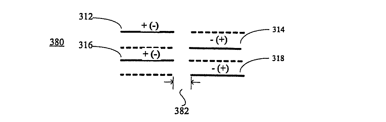
図3A〜3Cは、本発明の一実施形態による電極板のさまざまな図である。図3Aは、多層放射構造コンデンサ用の電極板302〜308の斜視図である。電極板302〜308はさらに、接触フィンガ、すなわちエクステンション312〜318をそれぞれ有している。図3Aに示されている電極板302〜308および接触フィンガ312〜318の寸法は実物大ではないことに留意されたい。一実施形態において、電極板312および316は第一の極性の電位に接続され、電極板314および318は他の極性の電位に接続される。誘電性材料(図3Aでは示していない)が電極板302〜308の間に配置されることに留意されたい。また、図3Aに示している電極板302〜308の数は例示的なものであることに留意されたい。一実施形態において、電極板412〜418は、銅、ニッケル、アルミニウムおよび他の合金のうちの一つ以上を含む。
3A-3C are various views of an electrode plate according to one embodiment of the present invention. FIG. 3A is a perspective view of
図3Bは電極板302〜308の上面図を示す。図3Cは電極板302〜308の底面図を示す。一実施形態において、電極板302および306は一方の極性の電荷を移動させ、電極板304および308は他の極性の電荷を移動させる。図3Cは、4つの接触フィンガ312〜318を示しており、接触フィンガ312および316は一方の極性の電位に接続され、接触フィンガ316および318は他の極性の電位に接続される。一実施形態においては、ギャップ382が寄生インダクタンスの値に影響を及ぼすことに留意されたい。好ましくは、ギャップ382は12ミルよりも小さく、より好ましくは8ミルよりも小さい。
FIG. 3B shows a top view of the electrode plates 302-308. FIG. 3C shows a bottom view of the electrode plates 302-308. In one embodiment,
図4Aは、本発明の一実施形態による多層コンデンサ400の分解斜視図である。コンデンサ400は複数の第一および第二の電極板412〜418と誘電性材料402〜410とを有している。セラミック化合物のような誘電性材料は、一実施形態においては、電極板間に挟まれる。図4Aに示されている誘電性材料402〜410の寸法は例示的なものであり、実物大ではないことに留意されたい。コンデンサ400はさらに、電気的な接続を提供するための第一および第二の外部接触部420および422を有している。本発明のもとにある概念は、コンデンサ400に電極が追加されても、あるいはコンデンサ400から電極が除かれても変わらない。
FIG. 4A is an exploded perspective view of a
図4Aを参照すると、第一の電極のそれぞれ412あるいは416は、第一の内部電極あるいは電極板としても知られ、第一の部分440と第二の部分すなわちエクステンション430とを有する。第一の部分440は第一の電極412の主要部分である。第二の部分430は接触部である。一実施形態において、コンデンサ400の幅434はコンデンサ400の高さ436よりも小さい。図4Aに示されている接触フィンガ430は、単なる例示的なものにすぎず、実物大ではないことに留意されたい。さらに、第一の電極412は接触フィンガを有してもよいことに留意されたい。
Referring to FIG. 4A, each
同様に、第二の電極のそれぞれ414あるいは418は、第一の部分442および第二の部分、すなわちエクステンション432を有している。第一の部分442は第二の電極418の主要部分である。第二の部分432は接触フィンガである。一実施形態において、接触フィンガ430および432は、第一および第二の外部接触部420および422への電気接続を与えするように用いられる。第一および第二の外部接触部420および422の間の距離424は、寄生インダクタンスを減らすように最小にされる。
Similarly, each of the
誘電性材料402〜410は、セラミック層あるいは誘電体とも呼ばれ、第一および第二の電極板412〜418の間に挟まれる。一実施形態において、誘電性材料402〜410は、チタン酸バリウム、チタン、ジルコン酸塩、および他のタイプのセラミック材料の一つ以上から形成される。
The
第一の外部接触部420は、外部端子あるいは外部リードとしても知られ、電極板412〜418に直交しており、第一の電極板412および416の接触フィンガ430に電気的に接続する。第一の外部接触部420は、プリント回路基板あるいは配線のようなさまざまな接続媒体を介して第一の電極412、416と他の装置との間での電気的な接続を提供するために用いられる。一実施形態においては、第一の外部接触部420は、プリント回路基板に接続するように構成される。他の実施形態においては、第一の外部接触部420は、他のコンデンサあるいはインダクタのような装置に接続するように構成される。例えば、図9Dおよび10Cを参照すると、これには積み重ねられた放射状のコンデンサが示されている。また第二の外部接触部422も、外部端子あるいは外部リードとしても知られるが、電極板412〜418に直交するように配置され、第二の電極層414、418の接触フィンガ432に電気的に接続する。大地の外部接触部422は、第二の電極412、416と他の装置との間での電気的な接続を提供するために用いられる。一実施形態においては、第二の外部接触部422は、プリント回路基板と接続するように構成される。他の実施形態においては、第二の外部接触部422は、他のコンデンサのような装置に接続するように構成される。
距離424は、最小空間あるいは最小距離あるいは所定最小距離とも呼ばれ、第一の外部接触部420と第二の外部接触部422との間の物理的な距離である。
The first
The
図4Bは、本発明の一実施形態による多層コンデンサ450の構成である。コンデンサ450は、外部接触部452および454、ギャップ456、ならびに本体456を有している。一実施形態において、外部接触部452および454は、図4Aに示す外部接触部420および422に対応する。同様に、ギャップ456の幅は図4Aに示す最小空間424に対応する。この実施形態では、コンデンサ450の幅460が高さ464よりも短い。他の実施形態では、高さ464はコンデンサ450の長さ462よりも長い。本発明の効果の一つは、PCB上の設置スペースを節約することが可能であるということに関連している。もし接触フィンガが追加あるいは省かれても、本発明のもとにある概念から逸脱することはないということに留意されたい。
FIG. 4B is a configuration of a
図5は、本発明の一実施形態による、プリント回路基板上に搭載された多層コンデンサを示すブロック図である。図5を参照すると、ブロック図500は、コンデンサ502と、接触部504〜510を通して接続されたプリント回路基板512とを有している。一実施形態においては、コンデンサ502は、多層セラミックコンデンサであり、第一の外部接触部506および第二の外部接触部504を有している。寄生インダクタンスを減らすために、外部接触部504および506は、最小距離518を隔てて配置される。プリント回路基板512は、金属トレース514および516と、コンデンサ502に接続するための金属の接触部508および510とを有している。ここで、プリント回路基板512が多層の金属トレースを有していても、本発明のもとにある概念は変らないということに留意されたい。
FIG. 5 is a block diagram illustrating a multilayer capacitor mounted on a printed circuit board according to one embodiment of the invention. Referring to FIG. 5, a block diagram 500 includes a
一実施形態において、コンデンサ502は、表面実装技術を用いてプリント回路基板512にそれをはんだづけすることで、実装される。他の実施形態においては、コンデンサ502は、接着剤あるいは他の接着材料を介してプリント回路基板上に機械的に実装されてもよい。デカップリングコンデンサに関してこのタイプの実装技術を採用することの利点は、容易に実装することができ、かつ再加工も容易であるからである。
In one embodiment, the
図6A〜6Dは、本発明の代替的な実施形態によるコンデンサの接触端子を示すブロック図である。図6Aを参照すると、ブロック図600は、3つの接触バー604〜610を有するバー構造のコンデンサの底面図である。一実施形態において、コンデンサの一方の極性の電極板が外側のバー604および606に接続され、もう一方の極性の電極板は内側のバー610に接続される。言い換えると、接触端子の一つはコンデンサの中央のバーに配置され、他の接触端子は2つの部分に分割されて、コンデンサ600の外側の縁に配置される。バー構造は、外部接触部に対して低い直列抵抗を与える。DC/DCコンバータのようないくつかのアプリケーションについては、比較的高性能のDC/DCコンバータを実現するためには、直列抵抗を最小にすることが必要である。さらに、高性能DC/DCコンバータあるいは電圧調整器は、内部の直列抵抗だけではなく、プリント回路基板に関連するトレースおよびビアを介して発生する直列抵抗をも最小にしなければならない。ある局面においては、バー端子構造は、プリント回路基板とコンデンサとの結合直列抵抗を減少させる。
コンデンサ用の交互に配置された接触端子を作成するために、より高次のバー構造を採用することもできる。端子自体について使用可能である接触面積が少なくなるほど、本発明による多層コンデンサの放射状構造は直列寄生インダクタンスを増加的に減らすのに対して、実効直列抵抗は増加するということにさらに留意されたい。したがって、より多くの数の外部接触部を大きなコンデンサのために用いてもよいということが本発明の効果である。
6A-6D are block diagrams illustrating the contact terminals of a capacitor according to an alternative embodiment of the present invention. Referring to FIG. 6A, a block diagram 600 is a bottom view of a bar-structured capacitor having three contact bars 604-610. In one embodiment, one polarity electrode plate of the capacitor is connected to the
Higher-order bar structures can also be employed to create alternating contact terminals for capacitors. It should be further noted that the smaller the contact area available for the terminal itself, the greater the effective series resistance, whereas the radial structure of the multilayer capacitor according to the present invention reduces the series parasitic inductance incrementally. Therefore, it is an advantage of the present invention that a greater number of external contacts may be used for large capacitors.
図6Bを参照すると、ブロック図630は、バー構造における3つの接触バー634〜640を有する外部接触部632の他の実施形態を示している。一実施形態において、コンデンサの一方の極性の電極板は内側のフィンガ640に接続され、もう一方の極性の電極板は外側のバー634および636に接続される。外部接触部632は、バー634〜636のような接触面をコンデンサ632の表面を越えて広げ、コンデンサ632の本体の角を接触面で包む技術を示している。接触面の面積を大きくすることによって、等価直列抵抗(ESR)は減少し、これがコンデンサの性能を向上させるのに効果的であることに留意されたい。従来のコンデンサの任意の底面積について、この技術は面積を30%増やすことができる。広げられた接触面を用いることの他の利点は、コンデンサとプリント回路基板との間でより強固な接続を作り出すことである。他の実施形態において、2つの接触バー634および636は、抵抗を減らすために接触面積をさらに増加させるべく、コンデンサ632の表面を越えて広がり、コンデンサ632の角を包むように構成されている。
Referring to FIG. 6B, a block diagram 630 illustrates another embodiment of an
図6Cは、接触バーの高次の構成660を示している。この構成660は、接触バー664から670の代替的な配置を示している。一実施形態において、接触バー664〜670の間の感覚は、コンデンサ632の寄生インダクタンスを減少させるように最小とされる。図6Dはコンデンサ682の接触バー684〜690の構成680を示している。接触バー684〜690の接触面が大きいことにより、構成680の低ESRが提供される。なお、高次の接触バーを4つのバーより増やしても本発明から逸脱することはない。一実施形態において、接触バー684〜690は、抵抗を減らすために接触面積をさらに増やすべく、コンデンサ682の表面を越えて広がり、そしてコンデンサ682の角を包むように配置されている。
FIG. 6C shows a
放射状構造のコンデンサは、一実施形態においては、高パワーDC/DCコンバータにおけるフィルタ機能を実行するために用いられる。DC/DCコンバータは、DC−DCコンバータとしても知られるが、DC入力電圧を受け取ってDC出力電圧を生成する装置である。普通、生成される出力は、入力とは異なった電圧レベルである。他の応用においては、DC/DCコンバータは、ノイズの遮断および/または電力調整等を提供するように用いられる。 Radial structure capacitors are used in one embodiment to perform the filter function in a high power DC / DC converter. A DC / DC converter, also known as a DC-DC converter, is a device that receives a DC input voltage and generates a DC output voltage. Usually, the output produced is at a different voltage level than the input. In other applications, DC / DC converters are used to provide noise rejection and / or power regulation and the like.
図6Eは、本発明の一実施形態による、図6Aに示されている構成のための多層コンデンサの分解斜視図である。電極板614および616は接触フィンガ618〜619を含んでおり、電極板615および617は接触フィンガ620を含んでいる。図6Eに示されている電極板614〜617および接触フィンガ618〜620の寸法は実物大ではないことに留意されたい。発明の利点および効果は、接触フィンガ618〜619が、電極板614〜617に対して若干小さい、あるいは大きいサイズとされたときに得られる。一実施形態において、電極板615および617は一方の極性に接続され、電極板614〜616はもう一方の極性に接続される。電極板614〜617の間には空間あるいは誘電性材料(図6Eには示していない)が挿入されることに留意されたい。また、図6Eに示されている電極板614〜617の数は例示的なものであることにも留意されたい。一実施形態において、電極板614〜617は、銅、ニッケル、アルミニウム、および他の合金のうちの一つ以上から形成される。
6E is an exploded perspective view of a multilayer capacitor for the configuration shown in FIG. 6A, according to one embodiment of the invention.
図6Fは、本発明の一実施形態による、図6Bに示された接触構造632に類似した外部接触バー646〜649を有するコンデンサ642を示している。一実施形態において、コンデンサ642の本体644は、図6Eに示されている複数の電極板614〜617を有している。外部接触部646〜648は、接触面積を最大にするために本体644の角を包み込んでいる。この実施形態において、外部接触部646〜648は一方の極性に接続され、外部接触部649はもう一方の極性に接続される。
FIG. 6F shows a
図6Gは、本発明の一実施形態による、図6Cに示されている構成のための多層コンデンサの分解斜視図である。電極板674〜677は接触フィンガ650〜656を有しており、電極板674および677は一方の極性に接続され、電極板675〜676はもう一方の極性に接続されている。図6Gに示されている電極板674〜677および接触フィンガ650〜656の寸法は実物大ではないことに留意されたい。発明の利点および効果は、接触フィンガ650〜656が電極板674〜677に対してわずかに小さい、あるいは大きいサイズとされたときに得られる。電極板674〜677の間には空間または誘電性材料(図6Gには示していない)が挿入されることに留意されたい。また図6Gに示されている電極板674〜677の数は例示的なものである。一実施形態において、電極板674〜677は銅、ニッケル、アルミニウムおよび他の合金のうちの一つ以上から形成される。
6G is an exploded perspective view of a multilayer capacitor for the configuration shown in FIG. 6C, according to one embodiment of the invention. The electrode plates 674-677 have contact fingers 650-656, the
図6Hは、本発明の一実施形態による、図6Dに示されている接触構造682に類似した外部接触バー693〜696を有するコンデンサ691を示している。一実施形態において、コンデンサ691の本体692は、図6Gに示されているように複数の電極板674〜677を有している。外部接触部693〜696は、接触面積を最大にするために本体692の角を包み込んでいる。一実施形態において、外部接触バー693〜695は、本体692の表側および裏側を包み込んでいることに留意されたい。
FIG. 6H shows a
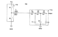
図7Aは、本発明の一実施形態による、多層コンデンサCを用いたDC−DCコンバータ700を概略的に示している。コンバータ700は、スイッチ電源702、インダクタLおよびコンデンサ704を有している。スイッチ電源702はさらに、第一にスイッチS1、第二のスイッチS2、Vcc、および接地電位を有している。また、コンデンサ704は、容量Cおよび寄生インダクタンスLparを有している。動作時には、インダクタLが電流変動を滑らかにし、コンデンサ704が出力における電圧変動を滑らかにする。コンバータ700は、DC−DC電圧調整器とも呼ばれることに留意されたい。
FIG. 7A schematically illustrates a DC-
図7Bは、DC/DCコンバータ750の他の構成を示している。コンバータ750は、スイッチ電源752、インダクタLおよびコンデンサ754を有している。コンバータ750はLC構成と呼ばれることもある。スイッチ電源752はさらに、第一のスイッチS1、第二のスイッチS2、Vcc、および接地電位GNDを有している。コンデンサ754は、それぞれ寄生インダクタンスL1、L2、L3を有する3つの容量要素C1、C2、C3を含んでいる。容量要素C1、C2、C3は、コンデンサ754の全体の容量を増やすべく、並列に接続されている。動作時には、インダクタLは電流変動を滑らかにし、コンデンサ754は出力における電圧変動を滑らかにする。
図8A〜8Cは、本発明の実施形態によるDC−DCコンバータの接続を示す構成である。図8Aは、DC/DCコンバータのようなLC構成を有する構成800を示している。構成800はコンデンサ801、インダクタLおよび出力を有している。コンデンサ801はさらに、2つの外部接触バー802および804を有しており、インダクタLの端子は接触バー802の一端に接続されている。出力は接触バー802の他端に接続されている。接触バー802の接続は、図7Aに示されているノードAの接続に対応している。代わりとなる実施形態においては、コンデンサ801は、一方の極性の2つの接触パッドを有しており、上のバー802の左側の部分がDC/DC電圧調整器のインダクタLの出力に接続され、上のバー802の右側の部分が電圧調整器の出力に接続される。下側のフィンガ804は基準電位に接続される。
FIG. 7B shows another configuration of the DC /
8A to 8C are configurations showing the connection of the DC-DC converter according to the embodiment of the present invention. FIG. 8A shows a
図8Bは代わりとなる実施形態を示している。構成810は、プリント回路基板820上に搭載されたDC−DCコンバータの接続を示している。一実施形態において、プリント回路基板820はさまざまなビア822〜828を有している。構成810は、コンデンサ811、インダクタLおよび出力を備えている。コンデンサ811はさらに、2つの外部接触バー812〜814を有しており、接触バー812〜814はさらに複数のビア822に連結される。インダクタLの端子はPCB上のトレースに接続されており、そのトレースはプリント回路基板820のビア824に接続され、出力はプリント回路基板82−の他のビア826に接続される。追加の外部接触バーを加えても本発明から逸脱しないということは当業者には明らかであろう。グランドあるいは基準電圧は、ビア828を介して右側のバー816に接続される。
FIG. 8B shows an alternative embodiment.
図8Cはコンデンサ850を含む代替的な構成840を示している。この構成840はさらに3つの外部接触バー852〜856を含んでいる。接触バー854は一方の極性の電位を提供し、接触バー852、856はコンデンサ850にグランドあるいは基準電位を提供する。ある応用においては、接触バーは伝送線として機能し、接触バー852および856はシールドを提供する。
FIG. 8C shows an
図9A〜9Dは、本発明の一実施形態による多層コンデンサのための積層構成を示している。図9Aは、第一の電極板904と第二の電極板906とを有する構成900を示している。なお、誘電性材料あるいは空気によるギャップが電極板の間に用いられてもよい。第一の電極板904は、上側の接触フィンガあるいはエクステンション908と下側の接触フィンガあるいはエクステンション910をさらに有している。第二の電極板906も、上側の接触フィンガあるいはエクステンション912と下側の接触フィンガあるいはエクステンション914とを有している。接触フィンガ908および910、912および914は、電極板904〜906に対して正しいスケールでは描かれていないことに留意されたい。
9A-9D illustrate a stacked configuration for a multilayer capacitor according to one embodiment of the present invention. FIG. 9A shows a
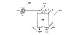
図9Bは、コンデンサ920の上側に外部接触バー926および928を、底に外部接触バー930および932を有するコンデンサ920を示している。コンデンサ920の本体922は、図9Aに示すように複数の電極板904および906を有している。一実施形態において、ギャップ924および925は、寄生インダクタンスを減らすように最小に保たれる。
FIG. 9B shows a
図9Cは、DC/DC電圧調整器のためのさまざまな構成要素間の物理的な接続の構成940を示している。インダクタLの出力端子は上側の外部接触バー926に接続されており、下側の外部接触バー930は出力端子に接続されている。他の外部接触バー932は、グランドあるいは基準電位に接続されている。
FIG. 9C shows a
図9Dは、概略図972に示すように、より大きなコンデンサを形成する2つのコンデンサ962および964が積層されている積層構成960を示している。一実施形態において、コンデンサ962および964を重ねるために、コンデンサ962の下側の外部接触バー982はコンデンサ964の上側の接触バー986に接続されており、コンデンサ962の下側の外部接触バー984はコンデンサ964の上側の外部接触バー988に接続されている。一つの局面において、概略図972におけるコンデンサ966はコンデンサ964とすることができ、コンデンサ968はコンデンサ962とすることができる。追加のコンデンサをコンデンサ962および/あるいは964に重ねても本発明から逸脱しないことは、当業者には明らかである。
FIG. 9D shows a
図10A〜10Eは、本発明による多層コンデンサのための積層構造を示している。図10Aは、第一の電極板1002および第二の電極板1004を有する構成1000を示している。第一の電極板1002は、第一の接触フィンガあるいはエクステンション1012および第二の接触フィンガ1013をさらに有している。一実施形態において、第一の接触フィンガ1012はコンデンサの側部に伸びており、第二の接触フィンガあるいはエクステンション1013はコンデンサの底部に伸びている。なお、接触フィンガ1012〜1015は電極板1002〜1004に対して正しいスケールでは描かれていないことに留意されたい。第二の電極板1004もまた、第一の接触フィンガあるいはエクステンション1014と第二の接触フィンガあるいはエクステンション1015を有しており、第一の接触フィンガ1014はコンデンサの側部に伸びており、第二の接触フィンガ1015はコンデンサの底部に伸びている。
10A-10E show a multilayer structure for a multilayer capacitor according to the present invention. FIG. 10A shows a
図10Bはコンデンサ1020の正面から見た図である。コンデンサ1002は、2つの側部接触バー1024および1026と、2つの底部接触バー1028および1030とを有している。コンデンサ1020の本体1022は、図10Aに示されている複数の第一および第二の電極板1002〜1004を有している。接触バー間の空間は、寄生インダクタンスを減らすように最小に保たれていなければならないことに留意されたい。一実施形態において、接触バー1024および1030はコンデンサ1020の一方の極性の端子であり、接触バー1026および1028はもう一方の極性の端子である。
FIG. 10B is a view from the front of the
図10Cは、より大きな容量素子を形成するように2つのコンデンサ1042および1044が積み重ねられている積層構成1040を示している。一実施形態において、積層は、コンデンサ1042の外部接触バー1048をコンデンサ1044の外部接触バー1050に接続することで実現される。他の接触バー1054〜1060は、プリント回路基板のような他の構成要素に接続するために用いられてもよい。
FIG. 10C shows a
図10Dは、第一の電極板1072と第二の電極板1074とを有する構成1070を示している。第一の電極板1072はさらに、第一の接触フィンガ1073と第二の接触フィンガ1075とを有している。一実施形態において、第一の接触フィンガ1073はコンデンサの底部に伸びており、第二の接触フィンガ1075はコンデンサの外表面のうちの一つに伸びている。第二の電極板1074は、第一の接触フィンガ1078と第二の接触フィンガ1079とを有している。第二の電極板1074の第一の接触フィンガ1078はコンデンサの底部に伸びており、第二の接触フィンガ1079はコンデンサの他の外表面に伸びている。一実施形態において、第一の電極板1072は一方の極性の電荷を伝搬し、第二の電極板1074は他の極性の電極を伝搬する。接触フィンガ1072〜1079は、電極板1072〜1074に対して正しいスケールでは描かれていないことに留意されたい。
FIG. 10D shows a
図10Eは、より大きな容量素子を形成するように2つのコンデンサ1082および1084が積み重ねられている積層構成1080を示している。一実施形態において、コンデンサ1082および1084は、図10Dに示されているコンデンサ装置1070である。図10Dおよび10Eを参照して、一実施形態において、接触フィンガ1075は外部接触バー1093に連結さR手織り、接触フィンガ1079は外部接触バー1092に連結されている。また、第一の電極板1072の接触フィンガ1073は外部接触バー1098に連結されており、第二の電極板1074の接触フィンガ1078は外部接触バー1097に連結されている。この実施形態において、接触フィンガ1092および1098は一つの極性の電荷を伝搬し、接触フィンガ1092および1097は他の極性の電荷を伝搬する。
FIG. 10E shows a
一実施形態において、積層は、コンデンサ1082の外部接触バー1088をコンデンサ1084の外部接触バー1099に接続することで実現される。この実施形態では、コンデンサ1082および1084は並列に接続されている。他の接触バー1094〜1098は、プリント回路基板のような他の構成要素に接続するように用いられてもよい。
In one embodiment, lamination is achieved by connecting the
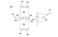
図11A〜11Cは、積層構成の他の実施形態を斜視図で示している。図11Aは、多層コンデンサの第一の電極板1102と第二の電極板1104とを示している。第一の電極板1102はさらに、第一の接触フィンガあるいはエクステンション1112と第二の接触フィンガあるいはエクステンション1113とを有している。一実施形態において、第一の接触フィンガ1112はコンデンサの左側部に伸び、第二の接触フィンガ1113はコンデンサの右側部に伸びている。接触フィンガ1112〜1114は、電極板1102および1104に対して正しいスケールでは描かれていないことに留意されたい。第二の電極板1104は、コンデンサの底部に伸びている接触フィンガあるいはエクステンション1114を有している。
11A-11C show other embodiments of a stacked configuration in perspective view. FIG. 11A shows a
図11Bはコンデンサ1120の正面図であり、コンデンサ1120は2つの側部接触バー1124および1126と一つの底部接触バー1128とを有している。コンデンサ1120の本体1122は、図11Aに示されている複数の第一および第二の電極板1102〜1104を有している。接触バー1124〜1128間の空間は、寄生インダクタンスを減らすために最小に保たれなければならないことに留意されたい。一実施形態において、接触バー1124および1126はコンデンサ1120の一方の極性の端子であり、接触バー1128は他の極性の端子である。
FIG. 11B is a front view of
図11Cはコンデンサ1120の他の正面図であり、コンデンサ1120は2つの側部接触バー1144〜1146と一つの底部接触バー1148とを有している。コンデンサ1140の本体1142は、図11Aに示されている複数の第一および第二の電極板1102〜1104を有している。接触バー1144〜1148以外は、コンデンサ1120の正面図は、コンデンサ1140の正面図に類似していることに留意されたい。接触バー1144〜1148はコンデンサ1140の本体1142の角を包み込んでいる。接触バー1144〜1148の間の空間は、寄生インダクタンスを減らすために最小に保たれなければならない。位置実施形態において、接触バー1144および1146はコンデンサ1140の一方の極性の端子であり、接触バー1148はもう一方の極性の端子である。
FIG. 11C is another front view of
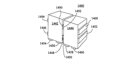
図14A〜14Bは、積層構成の他の実施形態の斜視図を示している。図14A〜14Bの実施形態は、図11A〜11Cにおける実施形態と比較して、両極性の側部電極をさらに有している。図14Aは、多層コンデンサの第一の電極板1402と第二の電極板1404とを示している。第一の電極板1402はさらに、第一の接触フィンガあるいはエクステンション1412と、第二の接触フィンガあるいはエクステンション1413と、第三の接触フィンガあるいはエクステンション1484とを有している。一実施形態において、第一の接触フィンガ1412はコンデンサの左側部に伸びており、第二の接触フィンガ1413はコンデンサの底部に伸びており、第三の接触フィンガ1434はコンデンサの右側部に伸びている。接触フィンガは電極板1402〜1404に対して正しいスケールでは描かれていないことに留意されたい。第二の電極板1404は第一の接触フィンガまたはエクステンション1482と、第二の接触フィンガまたはエクステンション1418と、第三の接触フィンガまたはエクステンション1482とを有している。そこに示されているように、第一の接触フィンガ1482はコンデンサの左側部に伸びており、第二の接触フィンガ1415はコンデンサの底部に伸びており、第三の接触フィンガ1414はコンデンサの右側部に伸びている。
14A-14B show perspective views of other embodiments of a stacked configuration. The embodiment of FIGS. 14A-14B further includes bipolar side electrodes as compared to the embodiment of FIGS. 11A-11C. FIG. 14A shows a
図14Bは積層構成1440を示しており、この構成においては2つのコンデンサ1442および1444が容量素子を構成するように積み重ねられている。一実施形態において、コンデンサ1442および1444は、図14Aに示されているコンデンサ装置1402である。コンデンサ1444を参照すると、接触フィンガ1484は外部接触バー1468に連結されており、接触フィンガ1414は外部接触バー1452に連結されており、接触フィンガ1413は外部接触バー1460に連結されており、接触フィンガ1415は外部接触バー1458に連結されており、接触フィンガ1412は外部接触バー1450に連結されており、接触フィンガ1482は外部接触バー1492に連結されている。コンデンサ1442は同様に構成されている。コンデンサ1490および1492は並べた構成に配置されており、この構成においてコンデンサ1442および1444は、電気的に連通している接触バー1490および1492と、同じく電気的に連通している接触バー1448および1450とによって、電気的に接続されている。この例示的な横に並べた構成において追加のコンデンサを積み重ねてもよいということは当業者には理解できるであろう。
FIG. 14B shows a
図14A〜14Bに示されている実施形態は直列にコンデンサを接続することを示しているが、並列にコンデンサを重ねるように再構成することもできる。 Although the embodiments shown in FIGS. 14A-14B show connecting capacitors in series, they can also be reconfigured to stack capacitors in parallel.
図12A〜12Bは、本発明の実施形態によるキャップを有するコンデンサを示している。図12Aは構成1200を示しており、本発明の一実施形態によるキャップ1212を有する積相されたコンデンサが示されている。構成1200は2つのコンデンサ1202および1204、キャップ1212およびプリント回路基板1220を有している。コンデンサ1204は、一実施形態においては、複数の外部接触バー1207〜1210を有している。外部接触バー1207および1208はコンデンサ1204の上面上にあり、外部接触バー1209および1210はコンデンサ1204の底面上にある。コンデンサ1204は接触バー1209および1210を介してプリント回路基板1220と接続されており、コンデンサ1202は接触バー1205〜1028を介してコンデンサ1204の上面上に積まれている。
12A-12B illustrate a capacitor having a cap according to an embodiment of the present invention. FIG. 12A shows a
一実施形態において、キャップ1212はコンデンサ1202および1204によって生成される熱を分散する機能を提供する。キャップ1212は、ハウジング、ホルダおよび/あるいは熱分散器として知られ、ここではこれらの用語は交換可能に用いられる。キャップ1212は特別な内部および外部フィンを有していてもよいが、これらは図12Aには示されていない。内部フィンは、積層されたコンデンサ1202〜1204間で熱を分散させるために用いられる。コンデンサは高周波数で動作しているときには熱くなる傾向であることに留意されたい。
In one embodiment, the
一実施形態において、放射構造のコンデンサを、より大きなコンデンサを構成するために縦方向に積み重ねられるためのホルダ1212内に配置することができる。ホルダあるいはキャップ1212は、プラスチックコンパウンドから形成されてもよい。あるいは、ホルダ1212は押し出しアルミニウム材料から形成されてもよい。ホルダ1212は複数のフィンを有しており、それらはホルダ1212の外表面部分への熱伝導路を提供するように用いられる。他の実施形態において、ホルダ1212は押し出しアルミニウムを用いて内部にチャンバを有するように構成されてもよい。この場合、それぞれのチャンバは、個々のコンデンサに適合するように設計される。熱分散は、コンデンサが高速で動作しているときには必要不可欠なものであることに留意されたい。
In one embodiment, radiating capacitor can be placed in a
図12Bは構成1250を示しており、これにおいて、本発明の一実施形態によるホルダ1256内に積層された形態のコンデンサを示している。構成1250は2つのコンデンサ1252および1254と、ホルダ、コンテナ、ハウジングあるいはキャップ1258と、プリント回路基板1270とを有している。一実施形態において、コンデンサ1252は複数の接触バー1262〜1264および1270を有しており、外部接触バー1262〜1264はコンデンサ1252の側部に伸びており、外部接触バー1270はコンデンサ1252の底部に伸びている。コンデンサ1254はコンデンサ1252と同様であり、これらは水平方向に積まれている。
FIG. 12B shows a
ホルダ1256は、熱伝導性材料から形成されてもよく、コンデンサ1252および1254によって生成される熱を分散させるように用いられてもよい。また、ホルダ1256はコンデンサ1252および1254の積み重ねを容易にする。一実施形態において、ホルダ1256とコンデンサ1252および1254との間の空間1258は、熱をより効果的に分散するための熱伝導性材料で満たされている。あるいは、コンデンサからの熱を分散させるために、オプションの素子1278が提供される。
図9Dおよび図10Cの積まれたコンデンサの配置が、例えば図6A〜6Dに示されているようにさまざまな外部端子の配置を含むことは本発明の範囲内である。 It is within the scope of the present invention that the stacked capacitor arrangements of FIGS. 9D and 10C include various external terminal arrangements as shown, for example, in FIGS.
ホルダ1256は、いかなる適切な材料から形成されたなんらかの適当なコンテナ、マガジン等を含んでもよいと考えられる。ホルダは、射出成形プロセスによって製造されてもよく、あるいは積層されるコンデンサはカプセル化プロセスによって互いに対して固定されてもよい。積層するコンデンサの数は、いかなる適切な数であってもよい。
It is contemplated that the
図13は、本発明の一実施形態による複数のコンデンサの積層構成1300を示している。構成1300は、複数のコンデンサの底面図1301とプリント回路基板(PCB)の上面図1320を含んでいる。底面図1301は、複数のコンデンサ1302〜1306の外部接触バー1310〜1314を含んでいる。各底面図は第一の極性の端子1310と第二の極性の端子1314を有している。端子1310と1314とを離間するために、空間1312が設けられる。一実施形態においては、空間1312は寄生インダクタンスを減らすために最小の距離である。
FIG. 13 shows a
PCB1320は第一の接触部1322と第二の接触部1324とを有しており、第一の接触部1332は一実施形態においては正極端子であり、第二の接触部1324は負極端子である。接触部1322および1324は空間1326によって離間されており、これは確実に接触部1322および1324間の最小の距離で離間させる。一実施形態においては、PCB1320は複数のコンデンサの並列接続を提供する。例えば、コンデンサ1302〜1306の接触部1310はPCB1320の第一の接触部1322に連結され、コンデンサ1302〜1306の接触部1314はPBCの第二の接触部1324に連結される。PCB上で複数のコンデンサを並列に接続することの利点は、歩留まりを上げることができることである。
The
発明の前述の説明においては、具体的な例示的な実施形態に言及した。しかし、本発明のより広い範囲を逸脱することなく、さまざまな改良および変更をそれに対して行ってもよいことは明白である。したがって明細書および図面は、限定的な意味ではなく、例示的なものとしてみなされるべきである。 In the foregoing description of the invention, reference has been made to specific exemplary embodiments. However, it will be apparent that various modifications and changes may be made thereto without departing from the broader scope of the invention. The specification and drawings are accordingly to be regarded in an illustrative rather than a restrictive sense.
以上、本発明を実施の形態を用いて説明したが、本発明の技術的範囲は上記実施の形態に記載の範囲には限定されない。上記実施の形態に、多様な変更または改良を加えることが可能であることが当業者に明らかである。その様な変更または改良を加えた形態も本発明の技術的範囲に含まれ得ることが、特許請求の範囲の記載から明らかである。 As mentioned above, although this invention was demonstrated using embodiment, the technical scope of this invention is not limited to the range as described in the said embodiment. It will be apparent to those skilled in the art that various modifications or improvements can be added to the above-described embodiment. It is apparent from the scope of the claims that the embodiments added with such changes or improvements can be included in the technical scope of the present invention.
本発明は、性能が向上したコンピュータおよびネットワーク通信に対応する高速・高密度の集積回路において、装置の信頼性を高めるために要求されるデカップリングコンデンサのような高度なノイズフィルタリング技術に適用可能である。 INDUSTRIAL APPLICABILITY The present invention can be applied to advanced noise filtering technology such as a decoupling capacitor required for enhancing the reliability of a device in a high-speed and high-density integrated circuit corresponding to computer and network communication with improved performance. is there.
202 多層コンデンサ
204、206 接触端子(接触バー)
208 プリント回路基板
302、304、306、306 電極板
312、314、316、318 接触フィンガ(エクステンション)
382 ギャップ
400 多層コンデンサ
412、414、416、418 電極板412〜418
402、404、406、408、410 誘電性材料
420 第一の外部接触部
422 第二の外部接触部
450 多層コンデンサ
452、454 外部接触部
456 本体
502 コンデンサ
504、506、508、510 接触部
512 プリント回路基板
514、516 トレース
600 コンデンサ
604、606、610 接触バー
614、615,616、617 電極板
618、619、620 接触フィンガ
632 コンデンサ
634、636、640 接触バー
642 コンデンサ
646、647、648 外部接触部
650、652、654、656 接触フィンガ
662 コンデンサ
664、666、668、670 接触バー
674、675、676、677 電極板
682 コンデンサ
684、686、688、690 接触バー
691 コンデンサ
693、694、695 外部接触バー
202
208 Printed
382
402, 404, 406, 408, 410
Claims (15)
前記m個の電極のそれぞれは間隔をあけて並列に配置されており、
mは3よりも大きい整数であり、
前記m個の電極のそれぞれは第一のエクステンションを備えており、
nは3よりも大きい整数であり、
前記n個の第一の外部端子は、前記コンデンサの第一の共通外表面上に配置されており、
前記m個の電極板の偶数番目のものの第一のエクステンションは、前記n個の第一の外部端子の偶数番目のものに連結されており、
前記m個の電極板の奇数番目のものの第一のエクステンションは、前記n個の第一の外部端子の奇数番目のものに連結されており、
前記n個の第一の外部端子は、寄生インダクタンスを最小にするように、お互いから予め定められた最小距離で配置されており、
前記n個の第一の外部端子が前記サブストレートに接続された場合において、当該コンデンサの前記m個の電極は前記サブストレートに対して垂直に配置され、
当該コンデンサの前記サブストレートより上の高さは、当該コンデンサの幅よりも大きく、
前記n個の第一の外部端子における第一のものと第二のものとが第一の極性を有し、かつ前記m個の電極のうちの隣り合うものにそれぞれ接続され、
前記n個の第一の外部端子における前記第一のものが前記第一のエクステンションの奇数番目のものの1つに接続され、
前記n個の第一の外部端子における第三のものが、前記第一の極性とは反対の第二の極性を有し、かつ前記第一のエクステンションの偶数番目のものの1つに接続され、
前記n個の第一の外部端子における前記第一のものが前記第一の共通外表面上における第一の列にあり、前記n個の第一の外部端子における前記第二のものが当該コンデンサの外側の縁であって、かつ前記第一の共通外表面上における第二の列にあり、
前記n個の第一の外部端子における前記第二のものが、前記第一のエクステンションのうちの偶数番目のものの別の1つに接続され、前記n個の第一の外部端子における前記第三のものが前記第一の列にあり、かつ前記外側の縁にあるコンデンサ。 A capacitor comprising m electrodes and n first external terminals having a bar structure, which is suitable for mounting on a substrate,
Each of the m electrodes is arranged in parallel with an interval between them,
m is an integer greater than 3 ,
Each of the m electrodes comprises a first extension;
n is an integer greater than 3 ,
The n first external terminals are disposed on a first common outer surface of the capacitor;
The first extension of the even-numbered ones of the m electrode plates is connected to the even-numbered ones of the n first external terminals,
The odd first one of the m electrode plates is connected to the odd first one of the n first external terminals,
The n first external terminals are arranged at a predetermined minimum distance from each other so as to minimize the parasitic inductance,
When the n first external terminals are connected to the substrate, the m electrodes of the capacitor are arranged perpendicular to the substrate,
Height above the substrate of the capacitor is much larger than the width of the capacitor,
A first one and a second one of the n first external terminals have a first polarity and are respectively connected to adjacent ones of the m electrodes;
The first of the n first external terminals is connected to one of the odd ones of the first extension;
A third one of the n first external terminals has a second polarity opposite to the first polarity and is connected to one of the even-numbered ones of the first extension;
The first one of the n first external terminals is in a first row on the first common outer surface, and the second one of the n first external terminals is the capacitor And in a second row on the first common outer surface,
The second one of the n first external terminals is connected to another one of the even-numbered ones of the first extensions, and the third one of the n first external terminals is connected to the third one. Capacitors in the first row and on the outer edge .
前記n個の第一の外部端子のうちの第四のものが前記第二の列にあり、
前記n個の第一の外部端子の前記第一のものは、前記n個の第一の外部端子の前記第三および前記第四のものに隣接し、かつ前記第二のものの対角に配置されており、
前記n個の第一の外部端子の前記第三のものは、前記第四のものの対角に配置されている請求項1から3のいずれかに記載のコンデンサ。 n is 4,
A fourth one of the n first external terminals is in the second row;
Said n number of first the first of the external terminals, adjacent ones of said n first the third and the fourth external terminal, and arranged diagonally of the second one Has been
4. The capacitor according to claim 1 , wherein the third one of the n first external terminals is disposed diagonally to the fourth one. 5.
前記コンデンサはs個の第二の外部端子を備えており、sは1よりも大きい整数であり、
前記s個の第二の外部端子は前記コンデンサの第二の共通外表面上に配置されており、
前記m個の電極板の偶数番目のものの第二のエクステンションは、前記s個の第二の外部端子のうちの偶数番目のものに連結されており、
前記m個の電極板の奇数番目のものの第二のエクステンションは、前記s個の外部端子のうちの奇数番目のものに連結されていることを特徴とする請求項1から4のいずれかに記載のコンデンサ。 Each of the m electrode plates has a second extension;
The capacitor includes s second external terminals, and s is an integer greater than 1,
The s second external terminals are disposed on a second common outer surface of the capacitor;
The even-numbered second extension of the m number of electrode plates is connected to the even-numbered number of the s second external terminals.
Odd ones of the second extension of the m electrode plates according to any one of claims 1 to 4, characterized in that it is connected to that of the odd-numbered of said s number of external terminals Capacitor.
前記コンデンサはs個の第二の外部端子を備えており、sは1よりも大きい整数であり、
前記s個の第二の外部端子のうちの偶数番目のものは、前記コンデンサの第三の外表面上に設けられており、
前記s個の第二の外部端子のうちの奇数番目のものは、前記コンデンサの第四の外表面上に設けられており、
前記m個の電極板のうちの偶数番目のものの前記第二のエクステンションは、前記s個の第二の外部端子の偶数番目のものと連結されており、
前記m個の電極板のうちの奇数番目のものの前記第二のエクステンションは、前記s個の第二の外部端子の奇数番目のものと連結されていることを特徴とする請求項1から4のいずれかに記載のコンデンサ。 Each of the m electrode plates has a second extension,
The capacitor includes s second external terminals, and s is an integer greater than 1,
An even number of the s second external terminals is provided on the third outer surface of the capacitor,
Wherein the s second of the number-th odd of the external terminal is provided to the fourth outer surface of the capacitor,
The second extension of the even-numbered one of the m electrode plates is connected to the even-numbered of the s second external terminals,
5. The odd numbered second extension of the m number of electrode plates is connected to the odd numbered number of the s second external terminals. 6. A capacitor according to any one of the above.
前記本体が、前記m個の電極板を有する、請求項1から7のいずれかに記載のコンデンサ。 The capacitor according to claim 1, wherein the main body includes the m electrode plates.
前記コンデンサの前記第四の外表面上に設けられた第四の外部端子と、 A fourth external terminal provided on the fourth outer surface of the capacitor;
を更に備え、Further comprising
前記m個の電極板のそれぞれが、更に第三のエクステンションを有し、 Each of the m electrode plates further has a third extension,
前記m個の電極板における前記第三のエクステンションのうちの偶数番目のものが前記第三の外部端子に接続され、 An even number of the third extensions of the m electrode plates is connected to the third external terminal,
前記m個の電極板における前記第三のエクステンションのうちの奇数番目のものが前記第四の外部端子に接続される、請求項7に記載のコンデンサ。 The capacitor according to claim 7, wherein odd-numbered ones of the third extensions of the m electrode plates are connected to the fourth external terminal.
前記m個の電極における前記第四のものが前記第二の極性を有し、 The fourth of the m electrodes has the second polarity;
前記m個の電極における前記第二のものと前記第三のものとが、前記m個の電極における前記第一のもの及び前記第四のものの間にある、請求項1から3及び5から10のいずれかに記載のコンデンサ。 1 1 to 3 and 5 to 10 wherein the second and the third of the m electrodes are between the first and the fourth of the m electrodes. The capacitor according to any one of the above.
前記m個の電極における前記第四のものが前記第二の極性を有し、 The fourth of the m electrodes has the second polarity;
前記m個の電極における前記第二のものと前記第三のものとが、前記m個の電極における前記第一のもの及び前記第四のものの間にある、請求項4のコンデンサ。 The capacitor of claim 4, wherein the second and third of the m electrodes are between the first and fourth of the m electrodes.
Applications Claiming Priority (4)
| Application Number | Priority Date | Filing Date | Title |
|---|---|---|---|
| US46887603P | 2003-05-06 | 2003-05-06 | |
| US46838003P | 2003-05-06 | 2003-05-06 | |
| US46947503P | 2003-05-08 | 2003-05-08 | |
| US10/694,306 US6950300B2 (en) | 2003-05-06 | 2003-10-27 | Ultra low inductance multi layer ceramic capacitor |
Related Parent Applications (1)
| Application Number | Title | Priority Date | Filing Date |
|---|---|---|---|
| JP2004134183A Division JP4045258B2 (en) | 2003-05-06 | 2004-04-28 | Ultra-low inductance multilayer ceramic capacitor |
Publications (2)
| Publication Number | Publication Date |
|---|---|
| JP2008022017A JP2008022017A (en) | 2008-01-31 |
| JP4498397B2 true JP4498397B2 (en) | 2010-07-07 |
Family
ID=33102453
Family Applications (2)
| Application Number | Title | Priority Date | Filing Date |
|---|---|---|---|
| JP2004134183A Expired - Lifetime JP4045258B2 (en) | 2003-05-06 | 2004-04-28 | Ultra-low inductance multilayer ceramic capacitor |
| JP2007206337A Expired - Lifetime JP4498397B2 (en) | 2003-05-06 | 2007-08-08 | Ultra-low inductance multilayer ceramic capacitor |
Family Applications Before (1)
| Application Number | Title | Priority Date | Filing Date |
|---|---|---|---|
| JP2004134183A Expired - Lifetime JP4045258B2 (en) | 2003-05-06 | 2004-04-28 | Ultra-low inductance multilayer ceramic capacitor |
Country Status (5)
| Country | Link |
|---|---|
| US (3) | US6950300B2 (en) |
| EP (1) | EP1480236B1 (en) |
| JP (2) | JP4045258B2 (en) |
| CN (1) | CN1551260B (en) |
| TW (1) | TWI338903B (en) |
Families Citing this family (70)
| Publication number | Priority date | Publication date | Assignee | Title |
|---|---|---|---|---|
| US6950300B2 (en) * | 2003-05-06 | 2005-09-27 | Marvell World Trade Ltd. | Ultra low inductance multi layer ceramic capacitor |
| US6885544B2 (en) * | 2003-09-24 | 2005-04-26 | Intel Corporation | Vertical capacitor apparatus, systems, and methods |
| US7068490B2 (en) * | 2004-04-16 | 2006-06-27 | Kemet Electronics Corporation | Thermal dissipating capacitor and electrical component comprising same |
| US6917510B1 (en) * | 2004-10-27 | 2005-07-12 | Kemet Corporation | Extended terminal ceramic SMD |
| US7136274B2 (en) * | 2004-10-28 | 2006-11-14 | Motorola, Inc. | Embedded multilayer printed circuit |
| US7235875B2 (en) * | 2004-12-09 | 2007-06-26 | International Business Machines Corporation | Modular heat sink decoupling capacitor array forming heat sink fins and power distribution interposer module |
| US7554172B2 (en) * | 2005-04-07 | 2009-06-30 | Tai-Her Yang | Multi-directional multiplexing radius convergence electrode |
| JP2007096272A (en) * | 2005-09-02 | 2007-04-12 | Sanyo Electric Co Ltd | Electrical elements and electrical circuits |
| US7414857B2 (en) | 2005-10-31 | 2008-08-19 | Avx Corporation | Multilayer ceramic capacitor with internal current cancellation and bottom terminals |
| US7697262B2 (en) * | 2005-10-31 | 2010-04-13 | Avx Corporation | Multilayer ceramic capacitor with internal current cancellation and bottom terminals |
| US8027146B2 (en) | 2005-12-26 | 2011-09-27 | Sanyo Electric Co., Ltd. | Electric circuit device enabling impedance reduction |
| US7292429B2 (en) * | 2006-01-18 | 2007-11-06 | Kemet Electronics Corporation | Low inductance capacitor |
| US8385047B2 (en) * | 2006-03-31 | 2013-02-26 | University Of Florida Research Foundation, Inc. | Integrated power passives |
| US7724498B2 (en) | 2006-06-30 | 2010-05-25 | Intel Corporation | Low inductance capacitors, methods of assembling same, and systems containing same |
| CN101523529B (en) * | 2006-10-06 | 2013-01-02 | 三洋电机株式会社 | Electrical components |
| DE102006054086A1 (en) * | 2006-11-16 | 2008-05-29 | Epcos Ag | Multilayer capacitor |
| US7961453B2 (en) * | 2007-01-09 | 2011-06-14 | Samsung Electro-Mechanics Co., Ltd. | Multilayer chip capacitor |
| US20080174931A1 (en) * | 2007-01-18 | 2008-07-24 | Skamser Daniel J | Vertical electrode layer design to minimize flex cracks in capacitors |
| US7920370B2 (en) * | 2007-02-05 | 2011-04-05 | Samsung Electro-Mechanics Co., Ltd. | Multilayer chip capacitor |
| US8493744B2 (en) * | 2007-04-03 | 2013-07-23 | Tdk Corporation | Surface mount devices with minimum lead inductance and methods of manufacturing the same |
| US8238116B2 (en) | 2007-04-13 | 2012-08-07 | Avx Corporation | Land grid feedthrough low ESL technology |
| US8289675B2 (en) | 2007-05-24 | 2012-10-16 | Daniel Devoe | Stacked multilayer capacitor |
| US7633739B2 (en) | 2007-05-24 | 2009-12-15 | Daniel Devoe | Stacked multilayer capacitor |
| KR100905879B1 (en) * | 2007-09-28 | 2009-07-03 | 삼성전기주식회사 | Stacked Capacitors |
| US20090147440A1 (en) * | 2007-12-11 | 2009-06-11 | Avx Corporation | Low inductance, high rating capacitor devices |
| US8446705B2 (en) * | 2008-08-18 | 2013-05-21 | Avx Corporation | Ultra broadband capacitor |
| US8094429B2 (en) * | 2009-06-22 | 2012-01-10 | Industrial Technology Research Institute | Multilayer capacitors and methods for making the same |
| CN102056404B (en) * | 2010-11-15 | 2013-01-23 | 浪潮电子信息产业股份有限公司 | Method for neutralizing capacitance of through hole |
| KR101536678B1 (en) * | 2011-04-07 | 2015-07-14 | 가부시키가이샤 무라타 세이사쿠쇼 | Electronic component |
| KR101558023B1 (en) * | 2011-08-26 | 2015-10-07 | 삼성전기주식회사 | Multilayer ceramic capacitor |
| KR101548774B1 (en) | 2011-08-26 | 2015-08-31 | 삼성전기주식회사 | Multilayer ceramic capacitor |
| US9564275B2 (en) | 2012-03-09 | 2017-02-07 | The Paper Battery Co. | Supercapacitor structures |
| DE102012104033B9 (en) * | 2012-05-08 | 2025-02-06 | Tdk Electronics Ag | ceramic multilayer capacitor |
| JP5853976B2 (en) * | 2012-06-12 | 2016-02-09 | 株式会社村田製作所 | Multilayer capacitor |
| CN103796426A (en) * | 2012-10-30 | 2014-05-14 | 联想(北京)有限公司 | Circuit module applying multi-layer chip capacitor and electronic equipment |
| KR101452058B1 (en) * | 2012-12-06 | 2014-10-22 | 삼성전기주식회사 | Multi-layered ceramic electronic component |
| JP6136916B2 (en) * | 2013-03-15 | 2017-05-31 | 株式会社村田製作所 | Multilayer capacitor |
| EP2973836A4 (en) | 2013-03-15 | 2017-03-22 | The Paper Battery Company, Inc. | Energy storage structures and fabrication methods thereof |
| KR101565643B1 (en) * | 2013-04-30 | 2015-11-03 | 삼성전기주식회사 | Multi-layered ceramic electronic part and board for mounting the same |
| KR20140038872A (en) * | 2013-07-17 | 2014-03-31 | 삼성전기주식회사 | Multi-layered ceramic capacitor part and board for mounting the same |
| CN104299785B (en) | 2013-07-17 | 2017-10-31 | 三星电机株式会社 | Multilayer ceramic capacitor and the plate with multilayer ceramic capacitor |
| KR20140038876A (en) | 2013-08-13 | 2014-03-31 | 삼성전기주식회사 | Multi-layered ceramic capacitor and board for mounting the same |
| US9653212B2 (en) | 2013-08-13 | 2017-05-16 | Samsung Electro-Mechanics Co., Ltd. | Multilayer ceramic capacitor and board for mounting thereof |
| US9583277B2 (en) | 2013-09-30 | 2017-02-28 | The Paper Battery Company, Inc. | Ultra-capacitor structures and electronic systems with ultra-capacitor structures |
| KR20140038915A (en) | 2013-10-31 | 2014-03-31 | 삼성전기주식회사 | Multi-layered ceramic capacitor and board for mounting the same |
| US20150114704A1 (en) | 2013-10-31 | 2015-04-30 | Samsung Electro-Mechanics Co., Ltd. | Multilayer ceramic capacitor and board having the same |
| KR101525689B1 (en) * | 2013-11-05 | 2015-06-03 | 삼성전기주식회사 | Multi-layered ceramic electroic components and mounting circuit thereof |
| JP6264858B2 (en) * | 2013-11-21 | 2018-01-24 | Tdk株式会社 | Electronic components |
| JP6167872B2 (en) * | 2013-11-21 | 2017-07-26 | Tdk株式会社 | Electronic components |
| US9672986B2 (en) * | 2014-01-13 | 2017-06-06 | Apple Inc. | Acoustic noise cancellation in multi-layer capacitors |
| KR102016485B1 (en) * | 2014-07-28 | 2019-09-02 | 삼성전기주식회사 | Multi layer ceramic capacitor and board having the same mounted thereon |
| KR102097323B1 (en) | 2014-08-14 | 2020-04-06 | 삼성전기주식회사 | Multi-layered ceramic capacitor and board for mounting the same |
| DE102015200717A1 (en) * | 2015-01-19 | 2016-07-21 | Efficient Energy Gmbh | capacitor |
| JP6451655B2 (en) * | 2016-01-15 | 2019-01-16 | 株式会社村田製作所 | Composite electronic components |
| KR102584978B1 (en) | 2016-06-01 | 2023-10-05 | 삼성전기주식회사 | Multilayered capacitor and board for mounting the same |
| CN117153563A (en) | 2017-05-15 | 2023-12-01 | 京瓷Avx元器件公司 | Multilayer capacitor and circuit board including same |
| WO2018235527A1 (en) * | 2017-06-19 | 2018-12-27 | 株式会社村田製作所 | Laminated element and lc filter |
| WO2019005616A1 (en) | 2017-06-29 | 2019-01-03 | Avx Corporation | Surface mount multilayer coupling capacitor and circuit board containing the same |
| US11004603B2 (en) | 2018-03-20 | 2021-05-11 | Avx Corporation | Vertical electrode decoupling/bypass capacitor |
| KR102514239B1 (en) | 2018-04-24 | 2023-03-27 | 삼성전기주식회사 | Multi-layered capacitor and board having the same mounted thereon |
| DE202018104586U1 (en) * | 2018-08-09 | 2019-11-19 | Sma Solar Technology Ag | DC link arrangement and inverter |
| CN114899009B (en) | 2019-01-28 | 2026-02-13 | 京瓷Avx元器件公司 | Multilayer ceramic capacitors with ultra-wideband performance |
| JP7653357B2 (en) | 2019-02-13 | 2025-03-28 | キョーセラ・エイブイエックス・コンポーネンツ・コーポレーション | Multilayer ceramic capacitors including conductive vias |
| JP2023085583A (en) * | 2020-05-12 | 2023-06-21 | パナソニックIpマネジメント株式会社 | Electric circuits for power supply of integrated circuits, capacitors and electric circuits with integrated circuits |
| US12387877B2 (en) | 2021-07-08 | 2025-08-12 | KYOCERA AVX Components Corporation | Multilayer ceramic capacitor |
| DE112023004552T5 (en) * | 2022-10-31 | 2025-08-21 | KYOCERA AVX Components Corporation | Multilayer capacitor |
| DE112023004553T5 (en) | 2022-10-31 | 2025-08-14 | KYOCERA AVX Components Corporation | Multilayer capacitor |
| JPWO2024111210A1 (en) * | 2022-11-24 | 2024-05-30 | ||
| US20250022661A1 (en) * | 2023-07-12 | 2025-01-16 | Kemet Electronics Corporation | Monolithic multilayered ceramic capacitor |
| TWI894908B (en) * | 2024-04-10 | 2025-08-21 | 國巨股份有限公司 | Embedded multi-layer ceramic capacitor |
Family Cites Families (90)
| Publication number | Priority date | Publication date | Assignee | Title |
|---|---|---|---|---|
| US26059A (en) * | 1859-11-08 | Improvement in sewing-machines | ||
| US3456215A (en) | 1964-09-02 | 1969-07-15 | Peter A Denes | High frequency low pass filter |
| US4085435A (en) * | 1976-06-14 | 1978-04-18 | Avx Corporation | Tantalum chip capacitor |
| US4059887A (en) * | 1976-06-14 | 1977-11-29 | Avx Corporation | Tantalum chip capacitor and method of manufacture |
| US4151579A (en) * | 1977-09-09 | 1979-04-24 | Avx Corporation | Chip capacitor device |
| US4297773A (en) * | 1978-11-16 | 1981-11-03 | Avx Corporation | Method of manufacturing a monolithic ceramic capacitor |
| US4347650A (en) * | 1980-09-22 | 1982-09-07 | Avx Corporation | Method of making marginless multi-layer ceramic capacitors |
| US4414844A (en) * | 1981-07-24 | 1983-11-15 | Avx Corporation | Rapid insulation resistance test for bismuth-containing ceramic capacitors |
| US4451845A (en) * | 1981-12-22 | 1984-05-29 | Avx Corporation | Lead frame device including ceramic encapsulated capacitor and IC chip |
| US4424551B1 (en) * | 1982-01-25 | 1991-06-11 | Highly-reliable feed through/filter capacitor and method for making same | |
| US4453199A (en) * | 1983-06-17 | 1984-06-05 | Avx Corporation | Low cost thin film capacitor |
| US4509103A (en) * | 1984-02-01 | 1985-04-02 | Avx Corporation | Low dissipation factor monolithic capacitor for high frequency applications |
| US4584629A (en) * | 1984-07-23 | 1986-04-22 | Avx Corporation | Method of making ceramic capacitor and resulting article |
| US4720767A (en) * | 1986-09-22 | 1988-01-19 | Avx Corporation | Internally fused variable value ceramic capacitor and circuit |
| US4680670A (en) * | 1986-09-29 | 1987-07-14 | Avx Corporation | Fail safe ceramic capacitor |
| US4731697A (en) * | 1987-05-05 | 1988-03-15 | Avx Corporation | Arc resistant trimable ceramic capacitor |
| US5134540A (en) * | 1988-05-06 | 1992-07-28 | Avx Corporation | Varistor or capacitor and method of making same |
| US5234641A (en) * | 1988-05-06 | 1993-08-10 | Avx Corporation | Method of making varistor or capacitor |
| US4831494A (en) * | 1988-06-27 | 1989-05-16 | International Business Machines Corporation | Multilayer capacitor |
| US4881308A (en) * | 1988-07-01 | 1989-11-21 | Avx Corporation | Method of terminating lead filled capacitor |
| US4935843A (en) * | 1988-07-01 | 1990-06-19 | Avx Corporation | Lead filled ceramic capacitor |
| US4853826A (en) * | 1988-08-01 | 1989-08-01 | Rogers Corporation | Low inductance decoupling capacitor |
| US4862318A (en) * | 1989-04-04 | 1989-08-29 | Avx Corporation | Method of forming thin film terminations of low inductance ceramic capacitors and resultant article |
| US4945452A (en) * | 1989-11-30 | 1990-07-31 | Avx Corporation | Tantalum capacitor and method of making same |
| US4984134A (en) * | 1990-01-16 | 1991-01-08 | Avx Corporation | Surface mount non-polar tantalum capacitor |
| US5072329A (en) * | 1991-04-01 | 1991-12-10 | Avx Corporation | Delamination resistant ceramic capacitor and method of making same |
| JPH0555084A (en) * | 1991-08-22 | 1993-03-05 | Murata Mfg Co Ltd | Laminated chip capacitor |
| JPH0562011A (en) * | 1991-09-03 | 1993-03-12 | Konica Corp | Image processor |
| US5198968A (en) * | 1992-07-23 | 1993-03-30 | Avx Corporation | Compact surface mount solid state capacitor and method of making same |
| US5216573A (en) * | 1992-08-21 | 1993-06-01 | Avx Corporation | Lead filled ceramic capacitor and method of making same |
| JP2976262B2 (en) * | 1992-09-25 | 1999-11-10 | 株式会社村田製作所 | Electronic component manufacturing method |
| US5357399A (en) * | 1992-09-25 | 1994-10-18 | Avx Corporation | Mass production method for the manufacture of surface mount solid state capacitor and resulting capacitor |
| US5517385A (en) * | 1992-11-19 | 1996-05-14 | International Business Machines Corporation | Decoupling capacitor structure |
| US5394295A (en) * | 1993-05-28 | 1995-02-28 | Avx Corporation | Manufacturing method for solid state capacitor and resulting capacitor |
| US5388024A (en) * | 1993-08-02 | 1995-02-07 | Avx Corporation | Trapezoid chip capacitor |
| US5495386A (en) * | 1993-08-03 | 1996-02-27 | Avx Corporation | Electrical components, such as capacitors, and methods for their manufacture |
| US5548474A (en) * | 1994-03-01 | 1996-08-20 | Avx Corporation | Electrical components such as capacitors having electrodes with an insulating edge |
| JP3287725B2 (en) * | 1994-06-07 | 2002-06-04 | キヤノン株式会社 | Exposure method and device manufacturing method using the same |
| JPH0855758A (en) * | 1994-08-10 | 1996-02-27 | Sumitomo Metal Ind Ltd | Multilayer capacitor |
| US5639507A (en) | 1995-05-03 | 1997-06-17 | Avx Corporation | Method of making a planar multi-layer capacitor |
| US5643432A (en) * | 1995-07-13 | 1997-07-01 | Avx Corporation | Selective anodization of capacitor anode body |
| US5880925A (en) * | 1997-06-27 | 1999-03-09 | Avx Corporation | Surface mount multilayer capacitor |
| US6058004A (en) | 1997-09-08 | 2000-05-02 | Delaware Capital Formation, Inc. | Unitized discrete electronic component arrays |
| JP2991175B2 (en) * | 1997-11-10 | 1999-12-20 | 株式会社村田製作所 | Multilayer capacitors |
| US6549395B1 (en) | 1997-11-14 | 2003-04-15 | Murata Manufacturing Co., Ltd | Multilayer capacitor |
| US6144547A (en) * | 1997-11-24 | 2000-11-07 | Avx Corporation | Miniature surface mount capacitor and method of making same |
| US6678927B1 (en) * | 1997-11-24 | 2004-01-20 | Avx Corporation | Miniature surface mount capacitor and method of making same |
| US6324048B1 (en) * | 1998-03-04 | 2001-11-27 | Avx Corporation | Ultra-small capacitor array |
| US5999398A (en) * | 1998-06-24 | 1999-12-07 | Avx Corporation | Feed-through filter assembly having varistor and capacitor structure |
| GB9824442D0 (en) * | 1998-11-06 | 1999-01-06 | Avx Ltd | Manufacture of solid state capacitors |
| US6282079B1 (en) * | 1998-11-30 | 2001-08-28 | Kyocera Corporation | Capacitor |
| JP3214472B2 (en) * | 1998-12-04 | 2001-10-02 | 日本電気株式会社 | Multilayer printed circuit board |
| JP2003051423A (en) * | 2001-08-03 | 2003-02-21 | Tdk Corp | Electronic component |
| JP4000701B2 (en) * | 1999-01-14 | 2007-10-31 | 株式会社村田製作所 | Multilayer capacitor |
| US6075700A (en) * | 1999-02-02 | 2000-06-13 | Compaq Computer Corporation | Method and system for controlling radio frequency radiation in microelectronic packages using heat dissipation structures |
| US6285542B1 (en) * | 1999-04-16 | 2001-09-04 | Avx Corporation | Ultra-small resistor-capacitor thin film network for inverted mounting to a surface |
| US6208501B1 (en) | 1999-06-14 | 2001-03-27 | Dielectric Laboratories, Inc. | Standing axial-leaded surface mount capacitor |
| US6751085B1 (en) * | 1999-07-08 | 2004-06-15 | Avx Limited | Solid state capacitors and methods of manufacturing them |
| GB9916048D0 (en) * | 1999-07-08 | 1999-09-08 | Avx Ltd | Solid state capacitors and methods of manufacturing them |
| GB9918852D0 (en) * | 1999-08-10 | 1999-10-13 | Avx Ltd | Manufacture of solid state capacitors |
| GB9922091D0 (en) * | 1999-09-17 | 1999-11-17 | Avx Ltd | Manufacture of solid state capacitors |
| US6262886B1 (en) * | 1999-09-30 | 2001-07-17 | Apple Computer, Inc. | Translucent protective covering for a computer housing |
| JP3489728B2 (en) * | 1999-10-18 | 2004-01-26 | 株式会社村田製作所 | Multilayer capacitors, wiring boards and high frequency circuits |
| US6327134B1 (en) | 1999-10-18 | 2001-12-04 | Murata Manufacturing Co., Ltd. | Multi-layer capacitor, wiring board, and high-frequency circuit |
| GB9926975D0 (en) * | 1999-11-15 | 2000-01-12 | Avx Ltd | Solid state capacitors and methods of manufacturing them |
| US6292351B1 (en) | 1999-11-17 | 2001-09-18 | Tdk Corporation | Multilayer ceramic capacitor for three-dimensional mounting |
| JP3489729B2 (en) | 1999-11-19 | 2004-01-26 | 株式会社村田製作所 | Multilayer capacitors, wiring boards, decoupling circuits, and high-frequency circuits |
| US6262877B1 (en) | 1999-11-23 | 2001-07-17 | Intel Corporation | Low inductance high capacitance capacitor and method of making same |
| US6441459B1 (en) | 2000-01-28 | 2002-08-27 | Tdk Corporation | Multilayer electronic device and method for producing same |
| JP3765225B2 (en) * | 2000-06-14 | 2006-04-12 | 株式会社村田製作所 | Chip-type multiple electronic components |
| JP2002057066A (en) * | 2000-08-10 | 2002-02-22 | Taiyo Yuden Co Ltd | Chip array and its manufacturing method |
| US6611421B2 (en) * | 2000-09-08 | 2003-08-26 | Avx Corporation | Non-polarized tantalum capacitor and capacitor array |
| JP4332634B2 (en) * | 2000-10-06 | 2009-09-16 | Tdk株式会社 | Multilayer electronic components |
| US6483692B2 (en) | 2000-12-19 | 2002-11-19 | Intel Corporation | Capacitor with extended surface lands and method of fabrication therefor |
| US6674635B1 (en) * | 2001-06-11 | 2004-01-06 | Avx Corporation | Protective coating for electrolytic capacitors |
| US6459561B1 (en) * | 2001-06-12 | 2002-10-01 | Avx Corporation | Low inductance grid array capacitor |
| US6636416B2 (en) * | 2001-06-14 | 2003-10-21 | Intel Corporation | Electronic assembly with laterally connected capacitors and manufacturing method |
| US6816354B2 (en) * | 2001-07-02 | 2004-11-09 | Avx Corporation | Single layer capacitor milled part |
| JP2003060463A (en) * | 2001-08-09 | 2003-02-28 | Murata Mfg Co Ltd | Layered lc composite component and manufacturing method therefor |
| US6757152B2 (en) * | 2001-09-05 | 2004-06-29 | Avx Corporation | Cascade capacitor |
| US6496355B1 (en) * | 2001-10-04 | 2002-12-17 | Avx Corporation | Interdigitated capacitor with ball grid array (BGA) terminations |
| US6545855B1 (en) | 2001-12-03 | 2003-04-08 | Motorola, Inc. | Low inductance termination for electronic components |
| US7054136B2 (en) * | 2002-06-06 | 2006-05-30 | Avx Corporation | Controlled ESR low inductance multilayer ceramic capacitor |
| US6864147B1 (en) * | 2002-06-11 | 2005-03-08 | Avx Corporation | Protective coating for electrolytic capacitors |
| JP4305808B2 (en) * | 2002-07-03 | 2009-07-29 | 太陽誘電株式会社 | Multilayer capacitor |
| US7016175B2 (en) * | 2002-10-03 | 2006-03-21 | Avx Corporation | Window via capacitor |
| US6870727B2 (en) * | 2002-10-07 | 2005-03-22 | Avx Corporation | Electrolytic capacitor with improved volumetric efficiency |
| US6784760B2 (en) * | 2002-11-06 | 2004-08-31 | John Mezzalingua Associates, Inc. | Step attenuator using frequency dependent components and method of effecting signal attenuation |
| US6898070B2 (en) * | 2002-12-19 | 2005-05-24 | Avx Corporation | Transmission line capacitor |
| US6950300B2 (en) * | 2003-05-06 | 2005-09-27 | Marvell World Trade Ltd. | Ultra low inductance multi layer ceramic capacitor |
-
2003
- 2003-10-27 US US10/694,306 patent/US6950300B2/en not_active Expired - Lifetime
-
2004
- 2004-04-07 CN CN2004100310216A patent/CN1551260B/en not_active Expired - Lifetime
- 2004-04-20 TW TW093110964A patent/TWI338903B/en not_active IP Right Cessation
- 2004-04-28 EP EP04010108.1A patent/EP1480236B1/en not_active Expired - Lifetime
- 2004-04-28 JP JP2004134183A patent/JP4045258B2/en not_active Expired - Lifetime
-
2005
- 2005-07-19 US US11/184,208 patent/US7230816B2/en not_active Expired - Lifetime
-
2007
- 2007-06-12 US US11/811,881 patent/US7701695B2/en not_active Expired - Lifetime
- 2007-08-08 JP JP2007206337A patent/JP4498397B2/en not_active Expired - Lifetime
Also Published As
| Publication number | Publication date |
|---|---|
| US7701695B2 (en) | 2010-04-20 |
| US20040223290A1 (en) | 2004-11-11 |
| US20080049377A1 (en) | 2008-02-28 |
| EP1480236A3 (en) | 2004-12-01 |
| US7230816B2 (en) | 2007-06-12 |
| US6950300B2 (en) | 2005-09-27 |
| TW200504773A (en) | 2005-02-01 |
| TWI338903B (en) | 2011-03-11 |
| CN1551260B (en) | 2010-05-12 |
| EP1480236B1 (en) | 2016-06-08 |
| JP4045258B2 (en) | 2008-02-13 |
| JP2004336041A (en) | 2004-11-25 |
| JP2008022017A (en) | 2008-01-31 |
| CN1551260A (en) | 2004-12-01 |
| US20050258511A1 (en) | 2005-11-24 |
| EP1480236A2 (en) | 2004-11-24 |
Similar Documents
| Publication | Publication Date | Title |
|---|---|---|
| JP4498397B2 (en) | Ultra-low inductance multilayer ceramic capacitor | |
| JP3897745B2 (en) | Multilayer capacitor and multilayer capacitor mounting structure | |
| KR102069627B1 (en) | Composite electronic component and board for mounting the same | |
| KR102064013B1 (en) | Composite electronic component and board for mounting the same | |
| US7292429B2 (en) | Low inductance capacitor | |
| US8045319B2 (en) | Controlled ESR decoupling capacitor | |
| CN104600974B (en) | Combined electronical assembly and the plate installed above for having the combined electronical assembly | |
| US7035079B1 (en) | Multilayered chip capacitor and multilayer chip capacitor array | |
| US20080158773A1 (en) | Multilayer capacitor array | |
| CN1716476A (en) | Multilayer Capacitor | |
| KR20070092150A (en) | Multilayer Capacitor and Its Mounting Structure | |
| KR101124109B1 (en) | Muti-layered ceramic capacitor | |
| JP2013239753A (en) | Multilayered ceramic capacitor | |
| KR101051620B1 (en) | Multilayer capacitor | |
| JP4739318B2 (en) | Multilayer chip capacitor | |
| JP2001284171A (en) | Laminated electronic component | |
| KR102016486B1 (en) | Composite electronic component and board for mounting the same | |
| JP3511569B2 (en) | Multilayer capacitors | |
| KR101444511B1 (en) | Muti-layered ceramic capacitor | |
| CN104811029B (en) | Combined electronical assembly and the plate for being provided with the combined electronical assembly | |
| CN112992541B (en) | Multilayer capacitor and board on which the multilayer capacitor is mounted | |
| KR100674823B1 (en) | Wiring Connection Structure of Multilayer Capacitor Array |
Legal Events
| Date | Code | Title | Description |
|---|---|---|---|
| A977 | Report on retrieval |
Free format text: JAPANESE INTERMEDIATE CODE: A971007 Effective date: 20090501 |
|
| A131 | Notification of reasons for refusal |
Free format text: JAPANESE INTERMEDIATE CODE: A131 Effective date: 20090519 |
|
| A601 | Written request for extension of time |
Free format text: JAPANESE INTERMEDIATE CODE: A601 Effective date: 20090819 |
|
| A602 | Written permission of extension of time |
Free format text: JAPANESE INTERMEDIATE CODE: A602 Effective date: 20090824 |
|
| A601 | Written request for extension of time |
Free format text: JAPANESE INTERMEDIATE CODE: A601 Effective date: 20090918 |
|
| A602 | Written permission of extension of time |
Free format text: JAPANESE INTERMEDIATE CODE: A602 Effective date: 20090928 |
|
| A521 | Request for written amendment filed |
Free format text: JAPANESE INTERMEDIATE CODE: A523 Effective date: 20091015 |
|
| TRDD | Decision of grant or rejection written | ||
| A01 | Written decision to grant a patent or to grant a registration (utility model) |
Free format text: JAPANESE INTERMEDIATE CODE: A01 Effective date: 20100330 |
|
| A01 | Written decision to grant a patent or to grant a registration (utility model) |
Free format text: JAPANESE INTERMEDIATE CODE: A01 |
|
| A61 | First payment of annual fees (during grant procedure) |
Free format text: JAPANESE INTERMEDIATE CODE: A61 Effective date: 20100413 |
|
| FPAY | Renewal fee payment (event date is renewal date of database) |
Free format text: PAYMENT UNTIL: 20130423 Year of fee payment: 3 |
|
| R150 | Certificate of patent or registration of utility model |
Ref document number: 4498397 Country of ref document: JP Free format text: JAPANESE INTERMEDIATE CODE: R150 Free format text: JAPANESE INTERMEDIATE CODE: R150 |
|
| FPAY | Renewal fee payment (event date is renewal date of database) |
Free format text: PAYMENT UNTIL: 20130423 Year of fee payment: 3 |
|
| FPAY | Renewal fee payment (event date is renewal date of database) |
Free format text: PAYMENT UNTIL: 20140423 Year of fee payment: 4 |
|
| R250 | Receipt of annual fees |
Free format text: JAPANESE INTERMEDIATE CODE: R250 |
|
| R250 | Receipt of annual fees |
Free format text: JAPANESE INTERMEDIATE CODE: R250 |
|
| R250 | Receipt of annual fees |
Free format text: JAPANESE INTERMEDIATE CODE: R250 |
|
| R250 | Receipt of annual fees |
Free format text: JAPANESE INTERMEDIATE CODE: R250 |
|
| R250 | Receipt of annual fees |
Free format text: JAPANESE INTERMEDIATE CODE: R250 |
|
| R250 | Receipt of annual fees |
Free format text: JAPANESE INTERMEDIATE CODE: R250 |
|
| R250 | Receipt of annual fees |
Free format text: JAPANESE INTERMEDIATE CODE: R250 |
|
| R250 | Receipt of annual fees |
Free format text: JAPANESE INTERMEDIATE CODE: R250 |
|
| S111 | Request for change of ownership or part of ownership |
Free format text: JAPANESE INTERMEDIATE CODE: R313113 |
|
| R371 | Transfer withdrawn |
Free format text: JAPANESE INTERMEDIATE CODE: R371 |
|
| S111 | Request for change of ownership or part of ownership |
Free format text: JAPANESE INTERMEDIATE CODE: R313113 |
|
| R350 | Written notification of registration of transfer |
Free format text: JAPANESE INTERMEDIATE CODE: R350 |
|
| R250 | Receipt of annual fees |
Free format text: JAPANESE INTERMEDIATE CODE: R250 |
|
| S111 | Request for change of ownership or part of ownership |
Free format text: JAPANESE INTERMEDIATE CODE: R313113 |
|
| S531 | Written request for registration of change of domicile |
Free format text: JAPANESE INTERMEDIATE CODE: R313531 |
|
| R350 | Written notification of registration of transfer |
Free format text: JAPANESE INTERMEDIATE CODE: R350 |
|
| R360 | Written notification for declining of transfer of rights |
Free format text: JAPANESE INTERMEDIATE CODE: R360 |
|
| R360 | Written notification for declining of transfer of rights |
Free format text: JAPANESE INTERMEDIATE CODE: R360 |
|
| R371 | Transfer withdrawn |
Free format text: JAPANESE INTERMEDIATE CODE: R371 |
|
| S111 | Request for change of ownership or part of ownership |
Free format text: JAPANESE INTERMEDIATE CODE: R313113 |
|
| R350 | Written notification of registration of transfer |
Free format text: JAPANESE INTERMEDIATE CODE: R350 |
|
| R250 | Receipt of annual fees |
Free format text: JAPANESE INTERMEDIATE CODE: R250 |
|
| R250 | Receipt of annual fees |
Free format text: JAPANESE INTERMEDIATE CODE: R250 |
|
| R250 | Receipt of annual fees |
Free format text: JAPANESE INTERMEDIATE CODE: R250 |
|
| EXPY | Cancellation because of completion of term |