JP4471444B2 - LIQUID CRYSTAL DISPLAY DEVICE, AND MOBILE PHONE AND PORTABLE INFORMATION TERMINAL DEVICE HAVING THE SAME - Google Patents
LIQUID CRYSTAL DISPLAY DEVICE, AND MOBILE PHONE AND PORTABLE INFORMATION TERMINAL DEVICE HAVING THE SAME Download PDFInfo
- Publication number
- JP4471444B2 JP4471444B2 JP2000098110A JP2000098110A JP4471444B2 JP 4471444 B2 JP4471444 B2 JP 4471444B2 JP 2000098110 A JP2000098110 A JP 2000098110A JP 2000098110 A JP2000098110 A JP 2000098110A JP 4471444 B2 JP4471444 B2 JP 4471444B2
- Authority
- JP
- Japan
- Prior art keywords
- liquid crystal
- crystal display
- pixel
- sub
- scanning lines
- Prior art date
- Legal status (The legal status is an assumption and is not a legal conclusion. Google has not performed a legal analysis and makes no representation as to the accuracy of the status listed.)
- Expired - Fee Related
Links
Images


Classifications
-
- G—PHYSICS
- G02—OPTICS
- G02F—OPTICAL DEVICES OR ARRANGEMENTS FOR THE CONTROL OF LIGHT BY MODIFICATION OF THE OPTICAL PROPERTIES OF THE MEDIA OF THE ELEMENTS INVOLVED THEREIN; NON-LINEAR OPTICS; FREQUENCY-CHANGING OF LIGHT; OPTICAL LOGIC ELEMENTS; OPTICAL ANALOGUE/DIGITAL CONVERTERS
- G02F1/00—Devices or arrangements for the control of the intensity, colour, phase, polarisation or direction of light arriving from an independent light source, e.g. switching, gating or modulating; Non-linear optics
- G02F1/01—Devices or arrangements for the control of the intensity, colour, phase, polarisation or direction of light arriving from an independent light source, e.g. switching, gating or modulating; Non-linear optics for the control of the intensity, phase, polarisation or colour
- G02F1/13—Devices or arrangements for the control of the intensity, colour, phase, polarisation or direction of light arriving from an independent light source, e.g. switching, gating or modulating; Non-linear optics for the control of the intensity, phase, polarisation or colour based on liquid crystals, e.g. single liquid crystal display cells
- G02F1/133—Constructional arrangements; Operation of liquid crystal cells; Circuit arrangements
-
- G—PHYSICS
- G09—EDUCATION; CRYPTOGRAPHY; DISPLAY; ADVERTISING; SEALS
- G09G—ARRANGEMENTS OR CIRCUITS FOR CONTROL OF INDICATING DEVICES USING STATIC MEANS TO PRESENT VARIABLE INFORMATION
- G09G3/00—Control arrangements or circuits, of interest only in connection with visual indicators other than cathode-ray tubes
- G09G3/20—Control arrangements or circuits, of interest only in connection with visual indicators other than cathode-ray tubes for presentation of an assembly of a number of characters, e.g. a page, by composing the assembly by combination of individual elements arranged in a matrix no fixed position being assigned to or needed to be assigned to the individual characters or partial characters
- G09G3/34—Control arrangements or circuits, of interest only in connection with visual indicators other than cathode-ray tubes for presentation of an assembly of a number of characters, e.g. a page, by composing the assembly by combination of individual elements arranged in a matrix no fixed position being assigned to or needed to be assigned to the individual characters or partial characters by control of light from an independent source
- G09G3/36—Control arrangements or circuits, of interest only in connection with visual indicators other than cathode-ray tubes for presentation of an assembly of a number of characters, e.g. a page, by composing the assembly by combination of individual elements arranged in a matrix no fixed position being assigned to or needed to be assigned to the individual characters or partial characters by control of light from an independent source using liquid crystals
- G09G3/3611—Control of matrices with row and column drivers
- G09G3/3648—Control of matrices with row and column drivers using an active matrix
- G09G3/3659—Control of matrices with row and column drivers using an active matrix the addressing of the pixel involving the control of two or more scan electrodes or two or more data electrodes, e.g. pixel voltage dependant on signal of two data electrodes
-
- G—PHYSICS
- G09—EDUCATION; CRYPTOGRAPHY; DISPLAY; ADVERTISING; SEALS
- G09G—ARRANGEMENTS OR CIRCUITS FOR CONTROL OF INDICATING DEVICES USING STATIC MEANS TO PRESENT VARIABLE INFORMATION
- G09G2300/00—Aspects of the constitution of display devices
- G09G2300/08—Active matrix structure, i.e. with use of active elements, inclusive of non-linear two terminal elements, in the pixels together with light emitting or modulating elements
- G09G2300/0809—Several active elements per pixel in active matrix panels
- G09G2300/0828—Several active elements per pixel in active matrix panels forming a digital to analog [D/A] conversion circuit
-
- G—PHYSICS
- G09—EDUCATION; CRYPTOGRAPHY; DISPLAY; ADVERTISING; SEALS
- G09G—ARRANGEMENTS OR CIRCUITS FOR CONTROL OF INDICATING DEVICES USING STATIC MEANS TO PRESENT VARIABLE INFORMATION
- G09G2300/00—Aspects of the constitution of display devices
- G09G2300/08—Active matrix structure, i.e. with use of active elements, inclusive of non-linear two terminal elements, in the pixels together with light emitting or modulating elements
- G09G2300/0809—Several active elements per pixel in active matrix panels
- G09G2300/0842—Several active elements per pixel in active matrix panels forming a memory circuit, e.g. a dynamic memory with one capacitor
-
- G—PHYSICS
- G09—EDUCATION; CRYPTOGRAPHY; DISPLAY; ADVERTISING; SEALS
- G09G—ARRANGEMENTS OR CIRCUITS FOR CONTROL OF INDICATING DEVICES USING STATIC MEANS TO PRESENT VARIABLE INFORMATION
- G09G2330/00—Aspects of power supply; Aspects of display protection and defect management
- G09G2330/02—Details of power systems and of start or stop of display operation
- G09G2330/021—Power management, e.g. power saving
-
- G—PHYSICS
- G09—EDUCATION; CRYPTOGRAPHY; DISPLAY; ADVERTISING; SEALS
- G09G—ARRANGEMENTS OR CIRCUITS FOR CONTROL OF INDICATING DEVICES USING STATIC MEANS TO PRESENT VARIABLE INFORMATION
- G09G3/00—Control arrangements or circuits, of interest only in connection with visual indicators other than cathode-ray tubes
- G09G3/20—Control arrangements or circuits, of interest only in connection with visual indicators other than cathode-ray tubes for presentation of an assembly of a number of characters, e.g. a page, by composing the assembly by combination of individual elements arranged in a matrix no fixed position being assigned to or needed to be assigned to the individual characters or partial characters
- G09G3/2007—Display of intermediate tones
- G09G3/2074—Display of intermediate tones using sub-pixels
Landscapes
- Physics & Mathematics (AREA)
- Engineering & Computer Science (AREA)
- General Physics & Mathematics (AREA)
- Crystallography & Structural Chemistry (AREA)
- Chemical & Material Sciences (AREA)
- Theoretical Computer Science (AREA)
- Computer Hardware Design (AREA)
- Nonlinear Science (AREA)
- Mathematical Physics (AREA)
- Optics & Photonics (AREA)
- Control Of Indicators Other Than Cathode Ray Tubes (AREA)
- Liquid Crystal Display Device Control (AREA)
- Liquid Crystal (AREA)
- Devices For Indicating Variable Information By Combining Individual Elements (AREA)
Description
【0001】
【発明の属する技術分野】
この発明は、液晶を用いて画像を表示するための液晶表示装置に関し、より特定的には、デジタルデータの映像信号に応じて階調表示が可能な液晶表示装置に関する。
【0002】
【従来の技術】
パーソナルコンピュータ、テレビジョン受像機や携帯電話機などのディスプレイパネルとして、液晶表示装置が用いられるようになってきている。液晶表示装置は、従来のディスプレイ装置と比較して、低消費電力化や省スペース化といった面でメリットが大きい。
【0003】
図8は、従来技術の液晶表示装置500の全体構成を示すブロック図である。
図8を参照して、液晶表示装置500は、行列状に配置される複数のピクセル1001を含む液晶表示部1002を備える。カラー液晶表示装置においては、1個のピクセル1001は、R(Red)、G(Green)およびB(Blue)の各1つの画素1005から構成される。
【0004】
画素1005は液晶表示部1002において行列状に配置されている。液晶表示装置500は、さらに、各画素行ごとに配置される垂直走査線1010および共通配線1012と、各画素列ごとに配置される水平走査線1011とを備える。
【0005】
図9は、画素1005の構成を示す回路図である。
図9を参照して、画素1005は、対向して設けられる画素電極と共通電極とを有する液晶表示素子1102を含む。以下においては、液晶表示素子の画素電極と接続されるノードを画素電極ノードNaと称し、共通電極と接続されるノードを共通電極ノードNbと称する。
【0006】
画素電極ノードNaと共通電極ノードNbとの間の電位差に応じて、液晶表示素子中の液晶の配向性が変化する。これに応じて、液晶表示素子の輝度が変化することによって、各画素の輝度をコントロールすることが可能となる。
【0007】
画素1005は、さらに、画素電極ノードNaと共通配線1012との間に設けられる保持容量1103と、垂直走査線1010をゲートに受けて、信号線1011と画素電極ノードNaとの間に電気的に結合されるTFT(Thin Film Transistor)素子1101とをさらに含む。
【0008】
画素1105においては、垂直走査線1010に正電圧を印加(活性化)することにより、TFT素子1001をオンして、水平走査線線1011の電位レベルを画素電極ノードNaに伝達することができる。液晶表示素子1102自体もキャパシタンスを有するので、この場合には液晶表示素子1102および保持容量1103がTFT素子1101のオンによって充電されることになる。
【0009】
一方、垂直走査線1010が非活性化されてTFT素子1001がオフされた場合には、画素電極ノードNaの電位レベルは、保持容量1103によって保持される。
【0010】
再び図8を参照して、液晶表示装置500は、各画素行を一定周期で順に選択するための垂直走査回路1003と、各画素列に対して、表示データに対応する電圧信号である表示信号を供給するための水平走査回路1006とをさらに備える。
【0011】
垂直走査回路1003は、シフトレジスタ回路1004と、バッファ回路1005とを含み、各画素行を一定周期で順に選択するために、垂直走査線1010を順に1本ずつ活性化して、正電圧を印加する。
【0012】
水平走査回路1006は、各画素列を一定周期で順に選択するためのシフトレジスタ回路1007およびバッファ回路1008と、表示信号線1013と水平走査線1011との間に設けられるスイッチ1009とを含む。スイッチ1009は、各画素列に対応して設けられ、対応する表示信号線1013と信号線水平走査線との間をオン/オフする。スイッチ1009は、一定周期の信号に基づいて、順番に1個ずつオンされる。表示信号線1013は、液晶表示装置500がカラー表示装置であることから、R、GおよびBの3画素に対応して、それぞれ1本ずつ設けられる。
【0013】
水平走査回路1006によって、1つの画素行に属するすべての画素に対して表示信号の書込が行なわれた後、すなわち1つの画素行に対する走査が完了すると、垂直走査回路1003は、次の画素行を選択するために、これまで選択されていた垂直走査線1010を非活性化して0もしくは負電圧を印加するとともに、次の垂直走査線1010を活性化して正電圧を印加する。
【0014】
次の画素行に対しても同様の走査が順次実行され、垂直走査回路1003がすべての画素行を走査(これを1フレームとも称する)した後に、再び先頭の垂直走査線1012が活性化されて正電圧が印加される。このように、すべての画素が1フレームごとに順次表示信号を書込まれることによって、画像の表示が実行されることとなる。
【0015】
【発明が解決しようとする課題】
このように、従来の技術の液晶表示装置500においては、画素電極ノードNaの電位レベルに応じた輝度が各画素において得られるので、各画素における表示を階調表示とするためには、階調に対応した電位レベルで構成されるアナログ信号を水平走査線から画素電極ノードNaに書込む必要があった。このため、液晶表示装置に外部から入力される表示データがデジタルデータである場合には、デジタル/アナログ信号変換を行なうことが必要である。
【0016】
これに対して、デジタル信号である表示信号に対応して階調表示を実行するための構成として、各画素を複数に分割する面積階調方式が知られている。
【0017】
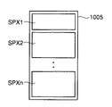
図10は、面積階調方式の概念を説明する図である。
図10を参照して、面積階調方式においては、画素1005を、複数の副画素SPX1〜SPXn(n:自然数)に分割される。副画素SPX1〜SPXnの各々は、デジタル信号に応じて、そのオン(最大輝度)およびオフ(最小輝度)が独立に制御される。したがって、各画素1005において、デジタルデータの表示信号に応じてオンする副画素を選択することにより、オン選択された副画素の面積に比例する階調的な輝度を得ることができる。
【0018】
しかしながら、このような、面積階調方式においては、階調数を高めるためには、画素の分割を増加させる必要がある。分割数を増加すると、画素1個当たりの大きさが増大し、表示解像度の低下や表示品位の低下を招くとという問題点があった。
【0019】
この発明は、このような問題点を解決するためになされたものであって、この発明の目的は、表示解像度などの表示品位を損なうことなく、デジタルデータによって高階調表示化が可能な液晶表示装置を提供することである。
【0020】
【課題を解決するための手段】
請求項1記載の液晶表示装置は、デジタル表示データに基づく情報を表示する液晶表示装置であって、行列状に配置される複数の垂直走査線および複数の水平走査線と、行列状に配置された複数の画素と、複数の垂直走査線を走査する垂直走査回路と、複数の水平走査線を走査する水平走査回路とを備える。各画素は、M個(M:2以上の自然数)の副画素を含む。複数の垂直走査線のそれぞれは、異なる行の副画素に接続され、複数の水平走査線のそれぞれは、第1および第2のデータ線を含むとともに、異なる列の画素に接続される。各副画素は、液晶表示素子と、液晶表示素子の両側に対向して配置される、共通電極および画素電極と、水平走査回路から対応するの第1のデータ線を介して供給され、表示データに対応する電位レベルを、対応する垂直走査線が走査されたことに応じて画素電極に伝達する第1のスイッチ素子とを有する。各画素は、M個の副画素のうちの2個にそれぞれ属する画素電極間に設けられ、接続制御ノードの電位に応じてオン/オフする副画素接続スイッチと、水平走査回路から対応する第2のデータ線を介して供給され、表示データに対応する電位レベルを、対応する垂直走査線が走査されたことに応じて副画素接続スイッチの接続制御ノードに伝達する第2のスイッチ素子とをさらに含む。各画素において第1のスイッチ素子がオン/オフした後に第2のスイッチがオン/オフする。
【0022】
請求項2記載の液晶表示装置は、請求項1記載の液晶表示装置であって、第1のデータ線は、共通電極に対応する電位および共通電極の電位レベルとの電位差が液晶表示素子の駆動電圧となる電位のいずれか一方を伝達する。
【0023】
請求項3記載の液晶表示装置は、請求項1記載の液晶表示装置であって、M個の副画素のそれぞれは、互いに異なる表示面積を有する。
【0024】
請求項4記載の液晶表示装置は、請求項3記載の液晶表示装置であって、各副画素は、液晶表示素子と並列に接続される保持容量素子をさらに有し、M個の副画素のそれぞれにおける、液晶表示素子および保持容量素子のキャパシタンスの和は互いに異なる。
【0025】
請求項5記載の液晶表示装置は、デジタル表示データに基づく情報を表示する液晶表示装置であって、行列状に配置される複数の垂直走査線および複数の水平走査線と、複数の垂直走査線に対応してそれぞれ配置される、複数の副垂直走査線、複数の第1の基準電位配線、および複数の第2の基準電位配線と、行列状に配置された複数の画素とを備える。各画素は、M個(M:2以上の自然数)の副画素を有する。各副画素は、複数の垂直走査線のうちの1本および複数の水平走査線のうちの1本と対応付けられている。各副画素は、液晶表示素子と、液晶表示素子の両側に対向して配置される、共通電極および画素電極と、対応する垂直走査線の電位に応じて、対応する水平走査線と第1の内部ノードとを接続する第1のスイッチ素子と、第1の内部ノードの電位レベルを保持するための制御用容量素子と、第1の内部ノードの電位レベルに応じて、第1および第2の基準電位配線のうちのいずれか一方を第2の内部ノードと接続する接続切換回路と、対応する副垂直走査線の電位に応じて、第2の内部ノードと画素電極とを接続する第2のスイッチ素子とをさらに有する。各画素は、M個の副画素のうちの2個にそれぞれ属する画素電極間に設けられた副画素接続スイッチをさらに有する。副画素接続スイッチは、複数の垂直走査線のうちの1本および複数の水平走査線のうちの1本と対応付けられており、対応する垂直走査線および水平走査線の電位レベルに応じてオン/オフする。
【0026】
請求項6記載の液晶表示装置は、請求項5記載の液晶表示装置であって、接続切換回路は、第1の基準電位配線と第2の内部ノードとの間に電気的に結合され、第1の内部ノードと接続されるゲート電極を有する第1導電型の薄膜トランジスタと、第1の基準電位配線と第2の内部ノードとの間に電気的に結合され、第1の内部ノードと接続されるゲート電極を有する第2導電型の薄膜トランジスタとを有する。
【0027】
請求項7記載の液晶表示装置は、請求項5記載の液晶表示装置であって、第1の基準電位配線は、共通電極に対応する電位を伝達し、第2の基準電位配線は、共通電極の電位レベルとの電位差が液晶表示素子の駆動電圧となる電位を伝達する。
【0028】
請求項8記載の液晶表示装置は、請求項5記載の液晶表示装置であって、複数の水平走査線は、各副画素のオン/オフ選択を行なうためのデジタル信号を伝達する。
【0029】
請求項9記載の携帯電話機は、デジタル信号に基づく情報を表示するための液晶表示部を備え、液晶表示部は、行列状に配置される複数の垂直走査線および複数の水平走査線と、複数の垂直走査線に対応してそれぞれ配置される、複数の副垂直走査線、複数の第1の基準電位配線、および複数の第2の基準電位配線と、行列状に配置された複数の画素とを含み、各画素は、M個(M:2以上の自然数)の副画素を有し、各副画素は、複数の垂直走査線のうちの1本および複数の水平走査線のうちの1本と対応付けられており、各副画素は、液晶表示素子と、液晶表示素子の両側に対向して配置される、共通電極および画素電極と、対応する垂直走査線の電位に応じて、対応する水平走査線と第1の内部ノードとを接続する第1のスイッチ素子と、第1の内部ノードの電位レベルを保持するための制御用容量素子と、第1の内部ノードの電位レベルに応じて、第1および第2の基準電位配線のうちのいずれか一方を第2の内部ノードと接続する接続切換回路と、対応する副垂直走査線の電位に応じて、第2の内部ノードと画素電極とを接続する第2のスイッチ素子とをさらに有し、各画素は、M個の副画素のうちの2個にそれぞれ属する画素電極間に設けられた副画素接続スイッチをさらに有し、副画素接続スイッチは、複数の垂直走査線のうちの1本および複数の水平走査線のうちの1本と対応付けられており、対応する垂直走査線および水平走査線の電位レベルに応じてオン/オフする。
【0030】
請求項10記載の携帯電話機は、請求項9記載の携帯電話機であって、複数の水平走査線は、各副画素のオン/オフ選択を行なうためのデジタル信号を伝達する。
【0031】
請求項11記載の携帯情報端末機器は、デジタル信号に基づく情報を表示するための液晶表示部を備え、液晶表示部は、行列状に配置される複数の垂直走査線および複数の水平走査線と、複数の垂直走査線に対応してそれぞれ配置される、複数の副垂直走査線、複数の第1の基準電位配線、および複数の第2の基準電位配線と、行列状に配置された複数の画素とを含み、各画素は、M個(M:2以上の自然数)の副画素を有し、各副画素は、複数の垂直走査線のうちの1本および複数の水平走査線のうちの1本と対応付けられており、各副画素は、液晶表示素子と、液晶表示素子の両側に対向して配置される、共通電極および画素電極と、対応する垂直走査線の電位に応じて、対応する水平走査線と第1の内部ノードとを接続する第1のスイッチ素子と、第1の内部ノードの電位レベルを保持するための制御用容量素子と、第1の内部ノードの電位レベルに応じて、第1および第2の基準電位配線のうちのいずれか一方を第2の内部ノードと接続する接続切換回路と、対応する副垂直走査線の電位に応じて、第2の内部ノードと画素電極とを接続する第2のスイッチ素子とをさらに有し、各画素は、M個の副画素のうちの2個にそれぞれ属する画素電極間に設けられた副画素接続スイッチをさらに有し、副画素接続スイッチは、複数の垂直走査線のうちの1本および複数の水平走査線のうちの1本と対応付けられており、対応する垂直走査線および水平走査線の電位レベルに応じてオン/オフする。
【0032】
請求項12記載の携帯情報端末機器は、請求項11記載の携帯情報端末機器であって、複数の水平走査線は、各副画素のオン/オフ選択を行なうためのデジタル信号を伝達する。
【0033】
【発明の実施の形態】
以下において、本発明の実施の形態について図面を参照して詳しく説明する。
【0034】
[実施の形態1]
図1は、本発明の実施の形態1に従う液晶表示装置100の全体構成を示すブロック図である。
【0035】
本発明の対象となる液晶表示装置は、カラー液晶表示装置およびモノクロ液晶表示装置のいずれにも適用可能な構成であるため、以下の説明においては、各画素に対応した構成について説明する。
【0036】
すなわち、液晶表示装置100を、カラー画像表示に使用する場合は、同様の構成で配置される各画素について、R、GおよびBのいずれかのカラーフィルタを設けることとして、3個の画素で1つの表示単位を形成することとすればよい。
【0037】
図1を参照して、液晶表示装置100は、行列状に配置された複数の画素20から構成される液晶表示部10を備える。各画素20は、副画素SPX1およびSPX2と、副画素接続回路25とを含む。図示しないが、行列状に配された他の画素20も副画素SPX1およびSPX2に分割されており、副画素接続スイッチ回路25をそれぞれが有している。
【0038】
したがって、液晶表示部10全体として、副画素SPX1、SPX2および副画素接続回路25は行列状に配置されることとなる。副画素および副画素接続回路の各行に対応して、独立の垂直走査線70が配置される。また、画素の各列に対応して水平走査線60が配置される。
【0039】
図1の例においては、画素20は、水平方向に沿って分割されているので、副画素SPX1およびSPX2と副画素接続回路25との間で水平走査線60が共有されている。
【0040】
水平走査線60は、表示信号に対応するデータを伝達する第1のデータ線62と、副画素間の接続を制御するための副画素接続信号を伝達する第2のデータ線65とを含む。また、副画素の各列に対応して、共通配線80が配置される。共通配線80は、共通電極ノードNbに対応する電位を供給する。
【0041】
副画素SPX1は、液晶表示素子22と、画素電極ノードNaと共通配線80との間に設けられる保持容量23と、垂直走査線70をゲートに受けて、第1のデータ線62と画素電極ノードNaとの間に電気的に結合されるスイッチ素子であるTFT素子21とをさらに含む。TFT素子21は、スイッチ素子の代表例として適用される。
【0042】
TFT素子21、液晶表示素子22および保持容量23は、図9で説明したTFT素子1101、液晶表示素子1102および保持容量1103にそれぞれ対応する。同様に、垂直走査線70、共通配線80および第1のデータ線62は、図7における垂直走査線1010、共通配線1012および水平走査線1011にそれぞれ対応する。その他の副画素の各々も、副画素SPX1と同様の構成を有する。
【0043】
垂直走査回路30は、図8で説明した垂直走査回路1003に対応し、垂直走査線70のうちの1本を、順番に一定期間ずつ活性化して正電圧を印加する。
【0044】
制御回路50は、副画素接続信号を副画素接続選択信号線52に出力し、表示信号を表示信号線54に出力する。水平走査回路40は、シフトレジスタ回路42およびバッファ回路45と、表示信号線54と第1のデータ線62との間に設けられるスイッチSW1と、副画素接続選択信号線52と第2のデータ線65との間に設けられるスイッチSW2とを備える。
【0045】
スイッチSW1およびSW2は、各画素列ごとに配置される。各画素列に対応して配置されるスイッチSW1およびSW2は、シフトレジスタ回路42およびバッファ回路45によって順にオンされ、水平走査回路40は、第1のデータ線62および第2のデータ線65を介して、各画素列に対して対応する表示信号および副画素接続信号を供給する。
【0046】
いわゆる、点順次駆動の場合には、1つの行に属する各副画素は、水平走査回路40によってそれぞれ表示信号を供給されて充電されていく。1つの行に対するすべての副画素に対する表示信号の供給が終了すると、垂直走査回路30は、次の行を選択するために、活性化の対象となる垂直走査線70を切換える。これにより、これまで活性化されていた垂直走査線70は非活性化されて、その電位レベルは0または負電圧となるので、対応するTFT素子21がオフされて、画素電極ノードNaの電位レベルが保持される。
【0047】
液晶表示装置100においては、各副画素に対応して、独立に表示信号を供給することが可能な回路構成としたので、それぞれの副画素のオン/オフ制御を独立に行なうことができ、表示信号がデジタルデータである場合においても、各画素20における階調表示を実行することが可能となる。
【0048】
液晶表示装置100においては、副画素SPX1とSPX2との間に副画素接続回路25を設けることにより、さらに多段階の階調表示が可能となる。
【0049】
副画素接続回路25は、接続制御ノードNcの電位レベルに応じて、副画素SPX1およびSPX2のそれぞれの画素電極ノード間を接続する副画素接続スイッチSWaと、垂直走査線70の電位レベルに応じて、第2のデータ線65と接続制御ノードNcとを接続する接続制御スイッチSWbとを有する。
【0050】
これにより、垂直走査線70の活性化によって指定されたタイミングにおいて副画素接続信号を第2のデータ線65を介して接続制御ノードNcに取込み、これに応じて副画素間の接続を制御することが可能となる。
【0051】
図2は、液晶表示装置100における副画素間の接続を説明するための概念図である。
【0052】
図2を参照して、副画素SPX1およびSPX2は、互いに異なる表示面積を有する。図2においては、副画素SPX1とSPX2との表示面積比をS:2Sとする。また、それぞれの副画素の容量値の比をC:4Cとする。ここで、副画素の容量値は、保持容量23および液晶表示素子22のキャパシタンスの和で与えられる。
【0053】
まず、副画素SPX1をオンして画素電極ノードに電位Vを書込み、副画素SPX2をオフする場合を考えると、副画素SPX1の画素電極ノードの電位(以下、単に画素電極電位とも称する)はVとなり、副画素SPX2の画素電極電位は0となる。
【0054】
各副画素における輝度が画素電極電位と表示面積との積に比例すると仮定すると、この場合における副画素間の接続前における画素輝度は、下記となる。
【0055】
V×S+0×2S=V・S
続いて、接続制御スイッチSWbに対応する垂直走査線に正電圧が印加されている期間中に、第2のデータ線に正電圧を印加することによって、副画素接続スイッチSWaをオンさせ、両副画素の画素電極を接続することができる。これに応じて、副画素SPX1およびSPX2間で電荷の再配分が生じ、両副画素の画素電極電位は変化することになる。
【0056】
すなわち、接続後の両副画素における画素電極電位をV′とすると、下記(1)式が成立する。
【0057】
V′×(C+4C)=V×C+0×4C …(1)
(1)式より、V′=V/5が得られる。したがって、副画素SPX1の画素電極の電位レベルはVからV/5に変化し、副画素SPX2の画素電極の電位レベルは0からV/5に変化する。
【0058】
副画素間の接続後における輝度は、下記となることから、副画素間を接続することによって、新たな階調を得ることができる。
【0059】
V/5×S+V/5×2S=3/5・V・S
次に、副画素SPX1と副画素SPX2とのオンおよびオフを入換えた場合、すなわち、副画素SPX2をオンして画素電極ノードに電位Vを書込み、副画素SPX1をオフした後に、両副画素の画素電極を接続する場合を考える。
【0060】
同様に、各副画素における輝度が画素電極電位と表示面積との積に比例すると仮定すると、副画素間の接続前における画素輝度は、下記となる。
【0061】
0×S+V×2S=2・V・S
同様に、接続後における画素電極電位をV′とすると、上記(1)式に代わって、下記(2)式が成立する。
【0062】
V′×(C+4C)=0×C+V×4C …(2)
(2)式より、V′=4/5・Vが得られる。これにより、副画素SPX1の画素電極の電位レベルは0から4/5・Vに変化し、副画素SPX2の画素電極の電位レベルはVから4/5・Vに変化する。
【0063】
一方、副画素間の接続後における輝度は、下記で示される。
4/5・V×S+4/5・V×2S=12/5・V・S
このように、副画素間を接続することによって、新たな階調を得ることができる。
【0064】
以上より、副画素SPX1(面積S,容量C)およびSPX2(面積2S,容量4C)に分割された画素においては、
(1)SPX1およびSPX2の両方がオフである場合(0)、
(2)SPX1のみがオンである場合(S・V)、
(3)SPX2のみがオンする場合(2・S・V)、および
(4)SPX1およびSPX2の両方がオンする場合(3・S・V)の4階調表示に加えて、上記の2通りの副画素間接続によって、
(5)副画素SPX1のみをオンした後に両副画素間を接続する場合(3/5・V・S)、および
(6)副画素SPX2のみをオンした後に、両副画素間を接続する場合(12/5・V・S)の2個の中間階調を得ることができる、これにより、各画素における副画素の分割数を増加させることなくさらに多くの階調表示を行なうことができる。
【0065】
上記のように、各副画素の表示面積および容量値は同一とせずに、異なる値とする方が、中間階調数を多くできる。副画素間の接続によって得られる中間階調のレベルは、副画素間の面積比および容量比によって調整することができる。
【0066】
液晶表示装置100においては各画素を2つの副画素に分割する場合について説明したが、各画素を3以上の複数個の副画素に分割してもよい。
【0067】
図3は、各画素を3個の副画素に分割した場合における副画素間の接続を説明する概念図である。
【0068】
図3を参照して、各画素を3個の副画素SPX1〜SPX3に分割した場合には、互いに独立にオン/オフ制御可能なスイッチSW12、SW23およびSW13を、それぞれの副画素間間に設けることにより、さらに多くの階調表示が可能となる。
【0069】
この場合においても、各副画素および副画素制御スイッチSW12,SW23,SW13を行列状に配置して、それぞれを垂直走査線および水平走査線に同期したタイミングで制御する構成とすることができる。
【0070】
[実施の形態2]
図4は、本発明の実施の形態2に従う液晶表示装置110の構成を示す概略ブロック図である。
【0071】
図4を参照して、液晶表示装置110は、実施の形態1に従う液晶表示装置100と比較して、副画素の構成が異なる。これに対応して、副画素の各行に対応して、垂直走査線70に加えて、副垂直走査線71、画像信号線75およびスイッチSW3が配置される。
【0072】
副垂直走査線71は、垂直走査回路30によって、1本ずつ順番に一定周期で活性化される。活性化時において、副垂直走査線71は、垂直走査線70と同様に、正電圧を印加される。
【0073】
スイッチSW3は、副垂直走査線71の活性化に応じてオンし、制御回路50が生成する基準電位を画像信号線75に伝達する。ただし、SW3を配置せずに、各画像信号線75に対して常に基準電位を供給する構成とすることも可能である。
【0074】
その他の構成については、図1で説明したのと同様であるので説明は繰返さない。
【0075】
図5は、実施の形態2に従う副画素の構成を説明する回路図である。
図5を参照して、実施の形態2に従う副画素SPX1′は、実施の形態1に従う副画素SPX1の構成と比較して、制御用容量素子26と、TFT素子27および28で構成される接続切換回路31と、スイッチ素子として用いられるTFT素子29とをさらに含む点で異なる。
【0076】
制御用容量素子26は、垂直走査線70の活性化に応じてTFT素子21を介して第1のデータ線62と接続される内部ノードNdと共通配線80との間に接続される。
【0077】
TFT素子27はn型であり、内部ノードNdと接続されるゲートを有し、画像信号線75と内部ノードNeとの間に電気的に結合される。TFT素子28は、TFT素子27と異なる導電型であり、内部ノードNdの電位レベルに応じてTFT素子27と相補的にオンする。TFT素子28は、内部ノードNdと接続されるゲートを有し、共通配線80と内部ノードNeとの間に電気的に結合される。
【0078】
TFT素子27および28は、内部ノードNdの電位レベルに応じて、相補的にオン/オフするので、接続切換回路31は、内部ノードNdの電位レベルに応じて、画素信号線75および共通配線80のうちのいずれか一方を内部ノードNeと接続する。
【0079】
TFT素子29は、副垂直走査線71と接続されるゲートを有し、内部ノードNeと画素電極ノードNaとの間に電気的に結合される。
【0080】
これにより、副垂直走査線71の活性化期間中において、内部ノードNdの電位レベルに応じて、画素信号線75および共通配線80のうちのいずれか一方が画素電極ノードNaと接続される。
【0081】
既に説明した副画素SPX1の場合と同様に、画素電極ノードNaの電位レベルは、保持容量23によって保持される。
【0082】
副画素SPX1′においては、副画素のオン/オフを示す表示信号は、第1のデータ線62によって伝達され、TFT素子21のオンに応じて、内部ノードNdに伝達されて、制御用容量素子26で保持される。したがって、次の行が走査され、対応する垂直走査線70が非活性化された場合においても、内部ノードNdには、一旦与えられた電位レベルが保持される。
【0083】
内部ノードNdに保持される電位レベルがHレベルであり、副画素SPX1′のオンが指示されている場合には、TFT素子27のオン状態が維持されるため、副垂直走査線71の活性化に応じて、画素電極ノードNaと画素信号線75とが接続される。反対に、内部ノードNdに0または負電圧が保持されて、副画素SPX1′のオフが指示されている場合には、TFT素子28がTFT素子27と相補的にオンされて、副垂直走査線71の活性化に応じて、画素電極ノードNaと共通配線80とが接続される。
【0084】
このように、画素電極ノードNaは、副画素へのオン/オフ指示を制御用容量素子26で保持し、副垂直走査線71の活性化に応じて、画素信号線75および共通配線80のいずれか一方と画素電極ノードNaとを周期的に接続することができる。この結果、同一画像を連続して表示する場合においては、一旦当該同一画像に対応する各副画素のオン/オフ指示を制御用容量素子26に保持させた後は、垂直走査線および水平走査線を駆動した高動作周波数の書込動作を実行することなく、副垂直走査線71を低い動作周波数で周期的に活性化することによって、所望の画像を連続表示することができる。
【0085】
したがって、同一画像の連続表示時における、水平走査回路および垂直走査回路の消費電力を削減することができる。
【0086】
さらに、画素信号線75および共通配線80と画素電極ノードNaとの接続が維持されるので、画素電極ノードNaの電位レベル変動は発生せず、反射率(輝度)の変化が生じない。
【0087】
ここで、画素信号線75によって伝達される基準電位を、画素電極に書込まれた電位が対向基板(共通電極)の電位レベルに液晶駆動電圧を加えた第1の電位レベル、または対向基板(共通電極)の電位レベルに液晶駆動電圧を減じた第2の電位レベルとなるように設定することにより、オンが指示された副画素における液晶の反射率は最大値(ノーマリホワイトモードでは最小値)となる。極性の異なる第1の電位レベルおよび第2の電位レベルを周期的に切換えて、基準電位とすることにより、液晶に常に同方向の電位が印可されることによる焼き付きの発生を防止できる。
【0088】
さらに、共通配線80によって伝達される電位レベルを、画素電極に書込まれる電位レベルが対向基板(共通電極)の電位レベルと等しくなるように設定すれば、オフが指定された副画素における液晶の反射率を最小値(ノーマリホワイトモードでは最大値)とすることができる。これにより、オンおよびオフがそれぞれ指示される副画素間におけるコントラストを最大に得ることができる。
【0089】
したがって、実施の形態2に従う液晶表示装置においては、副画素間の画素電極の接続を実現できる構成とともに、副画素に対するオン/オフ指示を副画素内部で保持することにより、同一画像を連続表示する場合における低消費電力化を図ることができる。
【0090】
さらに、最大輝度および最小輝度を安定的に出力できる副画素の構成とすることによって、コントラストに優れた多階調表示動作を可能とすることができる。
【0091】
[実施の形態2の変形例]
図6は、実施の形態2の変形例に従う携帯電話機200を示す図である。
【0092】
図6を参照して、携帯電話機200は、実施の形態2に従う液晶表示装置110を備える。携帯電話機の表示部は、液晶表示装置110の液晶表示部10によって形成される。したがって、表示部を構成する各副画素は、図5で説明した構成を有しているので、同一画像を連続して表示する場合において、低消費電力化を図ることができる。
【0093】
この特性は、いわゆる待ち受け時における低消費電力化要求が高い携帯電話機に適しており、実施の形態2に従う液晶表示装置110を備える携帯電話機200は、表示解像度などの表示品位を損なうことなくデジタルデータに基づく高階調表示を行なうとともに、低消費電力化によるバッテリー駆動時間の長期化を実現する。
【0094】
図7は、実施の形態2の変形例に従う携帯情報端末機器210を示す図である。
【0095】
図7を参照して、携帯情報端末機器210も、携帯電話機200と同様に、実施の形態2に従う液晶表示装置110を備えるので、同一画像を連続して表示する場合における低消費電力化を図ることができる。
【0096】
したがって、携帯情報端末機器210は、表示解像度などの表示品位を損なうことなくデジタルデータに基づく高階調表示を行なうとともに、低消費電力化によるバッテリー駆動時間の長期化を実現することができる。
【0097】
今回開示された実施の形態はすべての点で例示であって制限的なものではないと考えられるべきである。本発明の範囲は上記した説明ではなくて特許請求の範囲によって示され、特許請求の範囲と均等の意味および範囲内でのすべての変更が含まれることが意図される。
【0098】
【発明の効果】
請求項1および2に記載の液晶表示装置は、各副画素を2値的にオン/オフ制御することによって各画素における階調表示を行なう場合において、副画素の画素電極間を接続するスイッチを設けているので、表示可能な階調数を多くすることができる。
【0099】
請求項3記載の液晶表示装置は、各副画素の表示面積が異なるので、請求項1記載の液晶表示装置が奏する効果に加えて、さらに表示可能な階調数を多くすることができる。
【0100】
請求項4記載の液晶表示装置は、各副画素の容量値が異なるので、副画素の画素電極間を接続した場合に生じる電位レベルのバリエーションを増やすことができる。したがって、請求項1記載の液晶表示装置が奏する効果に加えて、さらに表示可能な階調数を多くすることができる。
【0101】
請求項5および6記載の液晶表示装置は、各副画素において、制御用容量素子によって内部ノードに保持される電位レベルに応じて、第1および第2の基準電位配線の一方と各副画素中の画素電極とを周期的に接続できる。したがって、同一画像を連続して表示する場合において、垂直走査線および水平走査線を駆動した高周波数の書込動作を実行する必要がなく、低消費電力化を図ることができる。
【0102】
請求項7記載の液晶表示装置は、共通電極との電位差がゼロおよび液晶駆動電位である2つの電位を、第1および第2の基準電位配線によってそれぞれ伝達するので、請求項5記載の液晶表示装置が奏する効果に加えて、副画素間の表示コントラストを強調することができる。
【0103】
請求項8記載の液晶表示装置は、請求項5記載の液晶表示装置が奏する効果に加えて、デジタル信号によって各画素の階調表示を行なうことができる。
【0104】
請求項9および10に記載の携帯電話機は、デジタル信号に基づいて各副画素を2値的にオン/オフ制御することによって各画素における階調表示を行なう場合において、副画素の画素電極間を接続するスイッチを設けているので、表示可能な階調数を多くすることができる。さらに、各副画素においては、制御用容量素子によって内部ノードに保持される電位レベルに応じて、第1および第2の基準電位配線の一方と各副画素中の画素電極とを周期的に接続できる。したがって、同一画像を連続して表示する、いわゆる待ち受け時において、垂直走査線および水平走査線を駆動した高周波数の書込動作を実行する必要がなく、低消費電力化を図ることができる。
【0105】
請求項11および12に記載の携帯情報端末機器は、デジタル信号に基づいて各副画素を2値的にオン/オフ制御することによって各画素における階調表示を行なう場合において、副画素の画素電極間を接続するスイッチを設けているので、表示可能な階調数を多くすることができる。さらに、各副画素においては、制御用容量素子によって内部ノードに保持される電位レベルに応じて、第1および第2の基準電位配線の一方と各副画素中の画素電極とを周期的に接続できる。したがって、同一画像を連続して表示する場合において、垂直走査線および水平走査線を駆動した高周波数の書込動作を実行する必要がなく、低消費電力化を図ることができる。
【図面の簡単な説明】
【図1】 本発明の実施の形態1に従う液晶表示装置100の全体構成を示すブロック図である。
【図2】 液晶表示装置100における副画素間の接続を説明するための概念図である。
【図3】 各画素を3個の副画素に分割した場合における副画素間の接続を説明する概念図である。
【図4】 本発明の実施の形態2に従う液晶表示装置110の構成を示す概略ブロック図である。
【図5】 実施の形態2に従う副画素の構成を説明する回路図である。
【図6】 実施の形態2の変形例に従う携帯電話機200を示す図である。
【図7】 実施の形態2の変形例に従う携帯情報端末装置210を示す図である。
【図8】 従来技術の液晶表示装置500の全体構成を示すブロック図である。
【図9】 画素1005の構成を示す回路図である。
【図10】 面積階調方式の概念を説明する図である。
【符号の説明】
10 液晶表示部、20 画素、25 副画素接続回路、26 制御用容量素子、30 垂直走査回路、40 水平走査回路、52 副画素接続選択信号線、54 表示信号線、60 水平走査線、62 第1のデータ線、65 第2のデータ線、70 垂直走査線、75 画像信号線、80 共通配線、Na 画素電極ノード、Nb 共通電極ノード、SPX1,SPX2,SPX3 副画素、SWa 副画素接続スイッチ、SWb 接続制御スイッチ。[0001]
BACKGROUND OF THE INVENTION
The present invention relates to a liquid crystal display device for displaying an image using liquid crystal, and more particularly to a liquid crystal display device capable of gradation display according to a video signal of digital data.
[0002]
[Prior art]
Liquid crystal display devices have come to be used as display panels for personal computers, television receivers, mobile phones and the like. The liquid crystal display device has a great merit in terms of low power consumption and space saving compared to a conventional display device.
[0003]
FIG. 8 is a block diagram showing an overall configuration of a conventional liquid
Referring to FIG. 8, liquid
[0004]
The
[0005]
FIG. 9 is a circuit diagram illustrating a configuration of the
Referring to FIG. 9, a
[0006]
The orientation of the liquid crystal in the liquid crystal display element changes according to the potential difference between the pixel electrode node Na and the common electrode node Nb. In response to this, the brightness of the liquid crystal display element changes, whereby the brightness of each pixel can be controlled.
[0007]
The
[0008]
In the pixel 1105, by applying (activating) a positive voltage to the
[0009]
On the other hand, when the
[0010]
Referring again to FIG. 8, the liquid
[0011]
The
[0012]
The
[0013]
After the
[0014]
The same scanning is sequentially executed for the next pixel row, and after the
[0015]
[Problems to be solved by the invention]
As described above, in the liquid
[0016]
On the other hand, an area gray scale method in which each pixel is divided into a plurality of parts is known as a configuration for executing gray scale display corresponding to a display signal which is a digital signal.
[0017]
FIG. 10 is a diagram for explaining the concept of the area gradation method.
Referring to FIG. 10, in the area gradation method, a
[0018]
However, in such an area gradation method, in order to increase the number of gradations, it is necessary to increase pixel division. When the number of divisions is increased, the size per pixel increases, which causes a problem that display resolution and display quality are deteriorated.
[0019]
The present invention has been made to solve such problems, and an object of the present invention is to provide a liquid crystal display capable of high gradation display by digital data without impairing display quality such as display resolution. Is to provide a device.
[0020]
[Means for Solving the Problems]
The liquid crystal display device according to
[0022]
Claim2The liquid crystal display device according to claim1The liquid crystal display device according to
[0023]
Claim3The liquid crystal display device described is the liquid crystal display device according to
[0024]
Claim4The liquid crystal display device according to claim3In the liquid crystal display device described above, each subpixel further includes a storage capacitor element connected in parallel with the liquid crystal display element, and the capacitances of the liquid crystal display element and the storage capacitor element in each of the M subpixels. The sums are different from each other.
[0025]
Claim5The described liquid crystal display deviceA liquid crystal display device for displaying information based on digital display data, a plurality of vertical scanning lines and a plurality of horizontal scanning lines arranged in a matrix,A plurality of sub-vertical scanning lines, a plurality of first reference potential wirings, and a plurality of second reference potential wirings respectively arranged corresponding to the plurality of vertical scanning lines.And a plurality of pixels arranged in a matrix. Each pixel has M (M: natural number of 2 or more) sub-pixels. Each subpixel is associated with one of a plurality of vertical scanning lines and one of a plurality of horizontal scanning lines.Each sub-pixelLiquid crystal display element, common electrode and pixel electrode arranged opposite to both sides of liquid crystal display element, and corresponding vertical scanning lineDepending on the potential ofWith corresponding horizontal scan lineA first switching element connecting to the first internal node, a control capacitive element for holding the potential level of the first internal node, and the first and second nodes according to the potential level of the first internal node, A connection switching circuit for connecting any one of the second reference potential wirings to the second internal node;Corresponding sub vertical scan lineAnd a second switch element for connecting the second internal node and the pixel electrode in accordance with the potential.Each pixel further includes a subpixel connection switch provided between pixel electrodes belonging to two of the M subpixels. The sub-pixel connection switch is associated with one of the plurality of vertical scanning lines and one of the plurality of horizontal scanning lines, and is turned on according to the potential level of the corresponding vertical scanning line and horizontal scanning line. / Turn off.
[0026]
Claim6The liquid crystal display device according to claim5In the liquid crystal display device described above, the connection switching circuit is electrically coupled between the first reference potential line and the second internal node, and has a gate electrode connected to the first internal node. A first conductivity type thin film transistor; and a second conductivity type thin film transistor having a gate electrode electrically coupled between the first reference potential wiring and the second internal node and connected to the first internal node. Have.
[0027]
Claim7The liquid crystal display device according to claim5The first reference potential wiring transmits a potential corresponding to the common electrode, and the second reference potential wiring has a potential difference from the potential level of the common electrode that is a driving voltage of the liquid crystal display element. The potential to be transmitted is transmitted.
[0028]
Claim8The liquid crystal display device according to claim5In the liquid crystal display device described above, the plurality of horizontal scanning lines transmit digital signals for performing on / off selection of each sub-pixel.
[0029]
Claim9The mobile phone described includes a liquid crystal display unit for displaying information based on a digital signal, and the liquid crystal display unit includes a plurality of vertical scanning lines and a plurality of horizontal scanning lines arranged in a matrix, and a plurality of vertical scannings. A plurality of sub-vertical scanning lines, a plurality of first reference potential wirings, a plurality of second reference potential wirings, and a plurality of pixels arranged in a matrix, each disposed corresponding to a line, Each pixel has M (M: a natural number of 2 or more) subpixels, and each subpixel is associated with one of a plurality of vertical scanning lines and one of a plurality of horizontal scanning lines. Each sub-pixel has a corresponding horizontal scanning line according to the potential of the liquid crystal display element, the common electrode and the pixel electrode arranged opposite to the both sides of the liquid crystal display element, and the corresponding vertical scanning line. A first switch element connecting the first internal node to the first internal node; A control capacitive element for holding the potential level of the internal node, and depending on the potential level of the first internal node, either one of the first and second reference potential wirings is connected to the second internal node. A connection switching circuit to be connected and a second switch element for connecting the second internal node and the pixel electrode in accordance with the potential of the corresponding sub vertical scanning line are further included. And a sub-pixel connection switch provided between pixel electrodes respectively belonging to two of the pixels, wherein the sub-pixel connection switch includes one of the plurality of vertical scanning lines and one of the plurality of horizontal scanning lines. Each line is associated with one line and is turned on / off according to the potential level of the corresponding vertical scanning line and horizontal scanning line.
[0030]
Claim 10The mobile phone described is claimed9The plurality of horizontal scanning lines transmit a digital signal for selecting on / off of each sub-pixel.
[0031]
Claim 11The described portable information terminal device includes a liquid crystal display unit for displaying information based on a digital signal. The liquid crystal display unit includes a plurality of vertical scanning lines and a plurality of horizontal scanning lines arranged in a matrix, and a plurality of liquid crystal display units. A plurality of sub-vertical scanning lines, a plurality of first reference potential wirings, a plurality of second reference potential wirings, and a plurality of pixels arranged in a matrix, which are respectively arranged corresponding to the vertical scanning lines. Each pixel has M (M: a natural number of 2 or more) subpixels, and each subpixel includes one of a plurality of vertical scanning lines and one of a plurality of horizontal scanning lines. Each sub-pixel is associated with a liquid crystal display element, a common electrode and a pixel electrode arranged opposite to both sides of the liquid crystal display element, and a corresponding horizontal scanning line according to the potential of the corresponding vertical scanning line. A first switch element connecting the scanning line and the first internal node; A control capacitive element for holding the potential level of the first internal node, and one of the first and second reference potential wirings is connected to the second in accordance with the potential level of the first internal node. A connection switching circuit connected to the internal node and a second switch element connecting the second internal node and the pixel electrode according to the potential of the corresponding sub-vertical scanning line are further included. A sub-pixel connection switch provided between pixel electrodes respectively belonging to two of the sub-pixels, wherein the sub-pixel connection switch includes one of a plurality of vertical scanning lines and a plurality of horizontal scanning lines. And is turned on / off according to the potential level of the corresponding vertical scanning line and horizontal scanning line.
[0032]
Claim 12The portable information terminal device described in claim 11In the portable information terminal device described above, the plurality of horizontal scanning lines transmit a digital signal for performing on / off selection of each sub-pixel.
[0033]
DETAILED DESCRIPTION OF THE INVENTION
Hereinafter, embodiments of the present invention will be described in detail with reference to the drawings.
[0034]
[Embodiment 1]
FIG. 1 is a block diagram showing an overall configuration of a liquid
[0035]
Since the liquid crystal display device that is the subject of the present invention can be applied to both a color liquid crystal display device and a monochrome liquid crystal display device, in the following description, a configuration corresponding to each pixel will be described.
[0036]
That is, when the liquid
[0037]
Referring to FIG. 1, a liquid
[0038]
Accordingly, the sub-pixels SPX1 and SPX2 and the
[0039]
In the example of FIG. 1, since the
[0040]
The horizontal scanning line 60 includes a
[0041]
The subpixel SPX1 receives the liquid
[0042]
The
[0043]
The
[0044]
The
[0045]
The switches SW1 and SW2 are arranged for each pixel column. The switches SW1 and SW2 arranged corresponding to each pixel column are sequentially turned on by the
[0046]
In the case of so-called dot sequential driving, each sub-pixel belonging to one row is supplied with a display signal by the
[0047]
Since the liquid
[0048]
In the liquid
[0049]
The
[0050]
Thus, the subpixel connection signal is taken into the connection control node Nc via the
[0051]
FIG. 2 is a conceptual diagram for explaining connections between sub-pixels in the liquid
[0052]
Referring to FIG. 2, subpixels SPX1 and SPX2 have different display areas. In FIG. 2, the display area ratio between the sub-pixels SPX1 and SPX2 is S: 2S. Further, the ratio of the capacitance values of the sub-pixels is C: 4C. Here, the capacitance value of the sub-pixel is given by the sum of the capacitance of the
[0053]
First, considering the case where the subpixel SPX1 is turned on, the potential V is written to the pixel electrode node, and the subpixel SPX2 is turned off, the potential of the pixel electrode node of the subpixel SPX1 (hereinafter also simply referred to as pixel electrode potential) is V Thus, the pixel electrode potential of the subpixel SPX2 becomes zero.
[0054]
Assuming that the luminance in each subpixel is proportional to the product of the pixel electrode potential and the display area, the pixel luminance before connection between the subpixels in this case is as follows.
[0055]
V × S + 0 × 2S = V · S
Subsequently, during the period in which the positive voltage is applied to the vertical scanning line corresponding to the connection control switch SWb, the sub-pixel connection switch SWa is turned on by applying a positive voltage to the second data line, so A pixel electrode of a pixel can be connected. Accordingly, charge redistribution occurs between the subpixels SPX1 and SPX2, and the pixel electrode potentials of both subpixels change.
[0056]
That is, when the pixel electrode potential in both sub-pixels after connection is V ′, the following equation (1) is established.
[0057]
V ′ × (C + 4C) = V × C + 0 × 4C (1)
From the equation (1), V ′ = V / 5 is obtained. Therefore, the potential level of the pixel electrode of the subpixel SPX1 changes from V to V / 5, and the potential level of the pixel electrode of the subpixel SPX2 changes from 0 to V / 5.
[0058]
Since the luminance after connection between the sub-pixels is as follows, a new gradation can be obtained by connecting the sub-pixels.
[0059]
V / 5 × S + V / 5 × 2S = 3/5 · V · S
Next, when the subpixel SPX1 and the subpixel SPX2 are turned on and off, that is, the subpixel SPX2 is turned on, the potential V is written to the pixel electrode node, and the subpixel SPX1 is turned off. Consider the case of connecting the pixel electrodes.
[0060]
Similarly, assuming that the luminance in each subpixel is proportional to the product of the pixel electrode potential and the display area, the pixel luminance before connection between the subpixels is as follows.
[0061]
0 × S + V × 2S = 2 · V · S
Similarly, when the pixel electrode potential after connection is V ′, the following equation (2) is established instead of the above equation (1).
[0062]
V ′ × (C + 4C) = 0 × C + V × 4C (2)
(From the equation (2), V ′ = 4/5 · V is obtained. As a result, the potential level of the pixel electrode of the subpixel SPX1 changes from 0 to 4/5 · V, and the potential level of the pixel electrode of the subpixel SPX2 changes from V to 4/5 · V.
[0063]
On the other hand, the luminance after connection between sub-pixels is shown below.
4/5 · V × S + 4/5 · V × 2S = 12/5 · V · S
In this way, a new gradation can be obtained by connecting the sub-pixels.
[0064]
As described above, in the pixel divided into the sub-pixels SPX1 (area S, capacity C) and SPX2 (area 2S, capacity 4C),
(1) When both SPX1 and SPX2 are off (0),
(2) When only SPX1 is on (SV),
(3) When only SPX2 is turned on (2 · S · V), and
(4) In addition to the four gradation display in the case where both SPX1 and SPX2 are turned on (3.S.V), the above-described two sub-pixel connections allow
(5) When only the subpixel SPX1 is turned on and then the subpixels are connected (3/5 · V · S), and
(6) After turning on only the sub-pixel SPX2, it is possible to obtain two intermediate gradations in the case of connecting both sub-pixels (12/5 · V · S). More gradations can be displayed without increasing the number of divisions.
[0065]
As described above, the number of intermediate gradations can be increased by setting the display area and the capacitance value of each subpixel to different values instead of being the same. The level of the intermediate gradation obtained by the connection between the subpixels can be adjusted by the area ratio and the capacitance ratio between the subpixels.
[0066]
In the liquid
[0067]
FIG. 3 is a conceptual diagram illustrating connections between sub-pixels when each pixel is divided into three sub-pixels.
[0068]
Referring to FIG. 3, when each pixel is divided into three subpixels SPX1 to SPX3, switches SW12, SW23 and SW13 that can be controlled on / off independently of each other are provided between the subpixels. As a result, a larger number of gradations can be displayed.
[0069]
Even in this case, the sub-pixels and the sub-pixel control switches SW12, SW23, SW13 can be arranged in a matrix and controlled at timing synchronized with the vertical scanning line and the horizontal scanning line.
[0070]
[Embodiment 2]
FIG. 4 is a schematic block diagram showing a configuration of liquid
[0071]
Referring to FIG. 4, liquid
[0072]
The sub
[0073]
The switch SW3 is turned on in response to the activation of the sub
[0074]
Other configurations are the same as those described with reference to FIG. 1, and therefore description thereof will not be repeated.
[0075]
FIG. 5 is a circuit diagram illustrating a configuration of a subpixel according to the second embodiment.
Referring to FIG. 5, subpixel SPX1 ′ according to the second embodiment is connected to control
[0076]
The
[0077]
The
[0078]
Since the
[0079]
The
[0080]
Thereby, during the activation period of the sub
[0081]
As in the case of the sub-pixel SPX1 already described, the potential level of the pixel electrode node Na is held by the holding
[0082]
In the sub-pixel SPX1 ′, a display signal indicating on / off of the sub-pixel is transmitted through the
[0083]
When the potential level held at the internal node Nd is H level and the on-state of the sub-pixel SPX1 ′ is instructed, the on-state of the
[0084]
As described above, the pixel electrode node Na holds the on / off instruction to the sub-pixel by the
[0085]
Therefore, the power consumption of the horizontal scanning circuit and the vertical scanning circuit during continuous display of the same image can be reduced.
[0086]
Further, since the connection between the
[0087]
Here, the reference potential transmitted by the
[0088]
Further, if the potential level transmitted by the
[0089]
Therefore, in the liquid crystal display device according to the second embodiment, the same image can be continuously displayed by holding the on / off instruction for the subpixel in the subpixel as well as the configuration capable of realizing the connection of the pixel electrode between the subpixels. In this case, power consumption can be reduced.
[0090]
Furthermore, a multi-tone display operation with excellent contrast can be achieved by employing a sub-pixel configuration that can stably output the maximum luminance and the minimum luminance.
[0091]
[Modification of Embodiment 2]
FIG. 6 is a diagram showing a
[0092]
Referring to FIG. 6,
[0093]
This characteristic is suitable for a mobile phone that is highly demanded to reduce power consumption during standby, and the
[0094]
FIG. 7 is a diagram showing a portable
[0095]
Referring to FIG. 7, portable
[0096]
Therefore, the portable
[0097]
The embodiment disclosed this time should be considered as illustrative in all points and not restrictive. The scope of the present invention is defined by the terms of the claims, rather than the description above, and is intended to include any modifications within the scope and meaning equivalent to the terms of the claims.
[0098]
【The invention's effect】
Claim1And2Since the liquid crystal display device described in (2) includes a switch for connecting the pixel electrodes of the subpixels when performing gradation display in each pixel by performing binary on / off control of each subpixel, The number of gradations that can be displayed can be increased.
[0099]
Claim3In the liquid crystal display device described above, since the display area of each sub-pixel is different, in addition to the effect exhibited by the liquid crystal display device according to
[0100]
Claim4In the liquid crystal display device described above, since the capacitance values of the sub-pixels are different, it is possible to increase variations in potential levels that occur when the pixel electrodes of the sub-pixels are connected. Therefore, in addition to the effect exhibited by the liquid crystal display device according to the first aspect, the number of gradations that can be displayed can be increased.
[0101]
Claim5and6In the liquid crystal display device described above, in each subpixel, one of the first and second reference potential wirings and the pixel electrode in each subpixel are connected in accordance with the potential level held in the internal node by the control capacitive element. Can be connected periodically. Therefore, in the case where the same image is continuously displayed, it is not necessary to perform a high-frequency writing operation in which the vertical scanning line and the horizontal scanning line are driven, and power consumption can be reduced.
[0102]
Claim7The liquid crystal display device described above transmits two potentials having a potential difference of zero with respect to the common electrode and a liquid crystal driving potential through the first and second reference potential wirings, respectively.5In addition to the effects exhibited by the described liquid crystal display device, display contrast between sub-pixels can be enhanced.
[0103]
Claim8The liquid crystal display device according to claim5In addition to the effects exhibited by the liquid crystal display device described, gradation display of each pixel can be performed by a digital signal.
[0104]
Claim9And 10The mobile phone described in 1 is provided with a switch for connecting the pixel electrodes of the subpixels when performing gradation display in each pixel by performing binary on / off control of each subpixel based on a digital signal. Therefore, the number of gradations that can be displayed can be increased. Further, in each sub-pixel, one of the first and second reference potential wirings and the pixel electrode in each sub-pixel are periodically connected in accordance with the potential level held in the internal node by the control capacitive element. it can. Therefore, at the time of so-called standby in which the same image is continuously displayed, it is not necessary to perform a high-frequency writing operation in which the vertical scanning line and the horizontal scanning line are driven, and low power consumption can be achieved.
[0105]
Claim 11And 12The portable information terminal device described in 1 is a switch that connects pixel electrodes of subpixels when performing gradation display in each pixel by performing binary on / off control of each subpixel based on a digital signal. Therefore, the number of gradations that can be displayed can be increased. Further, in each sub-pixel, one of the first and second reference potential wirings and the pixel electrode in each sub-pixel are periodically connected in accordance with the potential level held in the internal node by the control capacitive element. it can. Therefore, in the case where the same image is continuously displayed, it is not necessary to perform a high-frequency writing operation in which the vertical scanning line and the horizontal scanning line are driven, and power consumption can be reduced.
[Brief description of the drawings]
FIG. 1 is a block diagram showing an overall configuration of a liquid
2 is a conceptual diagram for explaining connections between sub-pixels in the liquid
FIG. 3 is a conceptual diagram illustrating connections between sub-pixels when each pixel is divided into three sub-pixels.
4 is a schematic block diagram showing a configuration of a liquid
FIG. 5 is a circuit diagram illustrating a configuration of a subpixel according to a second embodiment.
6 shows a
7 shows portable information
FIG. 8 is a block diagram showing an overall configuration of a conventional liquid
9 is a circuit diagram illustrating a configuration of a
FIG. 10 is a diagram illustrating the concept of an area gradation method.
[Explanation of symbols]
10 liquid crystal display unit, 20 pixels, 25 sub-pixel connection circuit, 26 control capacitor, 30 vertical scanning circuit, 40 horizontal scanning circuit, 52 sub-pixel connection selection signal line, 54 display signal line, 60 horizontal scanning line, 62 1 data line, 65 second data line, 70 vertical scanning line, 75 image signal line, 80 common wiring, Na pixel electrode node, Nb common electrode node, SPX1, SPX2, SPX3 subpixel, SWa subpixel connection switch, SWb Connection control switch.
Claims (12)
行列状に配置された複数の画素と、
前記複数の垂直走査線を走査する垂直走査回路と、
前記複数の水平走査線を走査する水平走査回路とを備え、
各前記画素は、M個(M:2以上の自然数)の副画素を含み、
前記複数の垂直走査線のそれぞれは、異なる行の前記副画素に接続され、
前記複数の水平走査線のそれぞれは、第1および第2のデータ線を含むとともに、異なる列の前記画素に接続され、
各前記副画素は、
液晶表示素子と、
前記液晶表示素子の両側に対向して配置される、共通電極および画素電極と、
前記水平走査回路から対応する前記の第1のデータ線を介して供給され、表示データに対応する電位レベルを、対応する前記垂直走査線が走査されたことに応じて前記画素電極に伝達する第1のスイッチ素子とを有し、
各前記画素は、
前記M個の副画素のうちの2個にそれぞれ属する前記画素電極間に設けられ、接続制御ノードの電位に応じてオン/オフする副画素接続スイッチと、
前記水平走査回路から対応する前記第2のデータ線を介して供給され、表示データに対応する電位レベルを、対応する前記垂直走査線が走査されたことに応じて前記副画素接続スイッチの接続制御ノードに伝達する第2のスイッチ素子とをさらに含み、
各前記画素において前記第1のスイッチ素子がオン/オフした後に前記第2のスイッチがオン/オフする、液晶表示装置。 A liquid crystal display device for displaying information based on digital display data, a plurality of vertical scanning lines and a plurality of horizontal scanning lines arranged in a matrix,
A plurality of pixels arranged in a matrix ;
A vertical scanning circuit for scanning the plurality of vertical scanning lines;
A horizontal scanning circuit that scans the plurality of horizontal scanning lines ,
Each of the pixels includes M (M: a natural number of 2 or more) subpixels,
Each of the plurality of vertical scanning lines is connected to the sub-pixel in a different row,
Each of the plurality of horizontal scanning lines includes first and second data lines and is connected to the pixels in different columns;
Each said subpixel is
A liquid crystal display element;
A common electrode and a pixel electrode disposed opposite to both sides of the liquid crystal display element ;
A first level supplied from the horizontal scanning circuit via the corresponding first data line and transmitting a potential level corresponding to display data to the pixel electrode in response to the scanning of the corresponding vertical scanning line. 1 switch element ,
Each said pixel is
A sub-pixel connection switch provided between the pixel electrodes belonging to each of two of the M sub-pixels and turned on / off according to the potential of a connection control node ;
Connection control of the sub-pixel connection switch according to the scanning of the vertical scanning line corresponding to the potential level supplied from the horizontal scanning circuit via the corresponding second data line and corresponding to display data. A second switch element for transmitting to the node ;
The liquid crystal display device in which the second switch is turned on / off after the first switch element is turned on / off in each pixel .
前記液晶表示素子と並列に接続される保持容量素子をさらに有し、
前記M個の副画素のそれぞれにおける、前記液晶表示素子および前記保持容量素子のキャパシタンスの和は互いに異なる、請求項3記載の液晶表示装置。Each said subpixel is
A storage capacitor element connected in parallel with the liquid crystal display element;
The liquid crystal display device according to claim 3 , wherein sums of capacitances of the liquid crystal display element and the storage capacitor element in each of the M sub-pixels are different from each other.
行列状に配置される複数の垂直走査線および複数の水平走査線と、
前記複数の垂直走査線に対応してそれぞれ配置される、複数の副垂直走査線、複数の第1の基準電位配線、および複数の第2の基準電位配線と、
行列状に配置された複数の画素とを備え、
各前記画素は、M個(M:2以上の自然数)の副画素を有し、
各前記副画素は、前記複数の垂直走査線のうちの1本および複数の水平走査線のうちの1本と対応付けられており、
各前記副画素は、
液晶表示素子と、
前記液晶表示素子の両側に対向して配置される、共通電極および画素電極と、
対応する前記垂直走査線の電位に応じて、対応する前記水平走査線と第1の内部ノードとを接続する第1のスイッチ素子と、
前記第1の内部ノードの電位レベルを保持するための制御用容量素子と、
前記第1の内部ノードの電位レベルに応じて、前記第1および第2の基準電位配線のうちのいずれか一方を第2の内部ノードと接続する接続切換回路と、
対応する前記副垂直走査線の電位に応じて、前記第2の内部ノードと前記画素電極とを接続する第2のスイッチ素子とをさらに有し、
各前記画素は、
前記M個の副画素のうちの2個にそれぞれ属する前記画素電極間に設けられた副画素接続スイッチをさらに有し、
前記副画素接続スイッチは、前記複数の垂直走査線のうちの1本および複数の水平走査線のうちの1本と対応付けられており、前記対応する垂直走査線および水平走査線の電位レベルに応じてオン/オフする、液晶表示装置。 A liquid crystal display device for displaying information based on digital display data,
A plurality of vertical scanning lines and a plurality of horizontal scanning lines arranged in a matrix;
Wherein the plurality of respectively arranged corresponding to the vertical scanning lines, a plurality of sub vertical scanning lines, a plurality of first reference potential wiring and a plurality of second reference potential line,
A plurality of pixels arranged in a matrix,
Each of the pixels has M (M: a natural number of 2 or more) subpixels,
Each of the sub-pixels is associated with one of the plurality of vertical scanning lines and one of the plurality of horizontal scanning lines;
Each said subpixel is
A liquid crystal display element;
A common electrode and a pixel electrode disposed opposite to both sides of the liquid crystal display element;
A first switch element that connects the corresponding horizontal scanning line and the first internal node according to the potential of the corresponding vertical scanning line ;
A control capacitive element for holding the potential level of the first internal node;
A connection switching circuit for connecting one of the first and second reference potential wirings to the second internal node according to the potential level of the first internal node;
According to the potential of the corresponding sub-vertical scanning lines, further have a second switching element for connecting the pixel electrode and the second internal node,
Each said pixel is
A subpixel connection switch provided between the pixel electrodes respectively belonging to two of the M subpixels;
The sub-pixel connection switch is associated with one of the plurality of vertical scanning lines and one of the plurality of horizontal scanning lines, and has a potential level of the corresponding vertical scanning line and horizontal scanning line. A liquid crystal display device that turns on and off in response .
前記第1の基準電位配線と前記第2の内部ノードとの間に電気的に結合され、前記第1の内部ノードと接続されるゲート電極を有する第1導電型の薄膜トランジスタと、
前記第2の基準電位配線と前記第2の内部ノードとの間に電気的に結合され、前記第1の内部ノードと接続されるゲート電極を有する第2導電型の薄膜トランジスタとを有する、請求項5記載の液晶表示装置。The connection switching circuit is
A first conductivity type thin film transistor having a gate electrode electrically coupled between the first reference potential wiring and the second internal node and connected to the first internal node;
And a second conductive type thin film transistor having a gate electrode electrically coupled between the second reference potential wiring and the second internal node and connected to the first internal node. 5. A liquid crystal display device according to 5 .
前記第2の基準電位配線は、前記共通電極の電位レベルとの電位差が前記液晶表示素子の駆動電圧となる電位を伝達する、請求項5記載の液晶表示装置。The first reference potential wiring transmits a potential corresponding to the common electrode,
The liquid crystal display device according to claim 5 , wherein the second reference potential wiring transmits a potential at which a potential difference from a potential level of the common electrode becomes a driving voltage for the liquid crystal display element.
前記液晶表示部は、
行列状に配置される複数の垂直走査線および複数の水平走査線と、
前記複数の垂直走査線に対応してそれぞれ配置される、複数の副垂直走査線、複数の第1の基準電位配線、および複数の第2の基準電位配線と、
行列状に配置された複数の画素とを含み、
各前記画素は、M個(M:2以上の自然数)の副画素を有し、
各前記副画素は、前記複数の垂直走査線のうちの1本および複数の水平走査線のうちの1本と対応付けられており、
各前記副画素は、
液晶表示素子と、
前記液晶表示素子の両側に対向して配置される、共通電極および画素電極と、
対応する前記垂直走査線の電位に応じて、対応する前記水平走査線と第1の内部ノードとを接続する第1のスイッチ素子と、
前記第1の内部ノードの電位レベルを保持するための制御用容量素子と、
前記第1の内部ノードの電位レベルに応じて、前記第1および第2の基準電位配線のうちのいずれか一方を前記第2の内部ノードと接続する接続切換回路と、
対応する前記副垂直走査線の電位に応じて、前記第2の内部ノードと前記画素電極とを接続する第2のスイッチ素子とをさらに有し、
各前記画素は、
前記M個の副画素のうちの2個にそれぞれ属する前記画素電極間に設けられた副画素接続スイッチをさらに有し、
前記副画素接続スイッチは、前記複数の垂直走査線のうちの1本および複数の水平走査線のうちの1本と対応付けられており、前記対応する垂直走査線および水平走査線の電位レベルに応じてオン/オフする、携帯電話機。A liquid crystal display for displaying information based on digital signals
The liquid crystal display unit
A plurality of vertical scanning lines and a plurality of horizontal scanning lines arranged in a matrix;
A plurality of sub-vertical scanning lines, a plurality of first reference potential wirings, and a plurality of second reference potential wirings, which are respectively arranged corresponding to the plurality of vertical scanning lines;
A plurality of pixels arranged in a matrix,
Each of the pixels has M (M: a natural number of 2 or more) subpixels,
Each of the sub-pixels is associated with one of the plurality of vertical scanning lines and one of the plurality of horizontal scanning lines;
Each said subpixel is
A liquid crystal display element;
A common electrode and a pixel electrode disposed opposite to both sides of the liquid crystal display element;
A first switch element that connects the corresponding horizontal scanning line and the first internal node according to the potential of the corresponding vertical scanning line;
A control capacitive element for holding the potential level of the first internal node;
A connection switching circuit for connecting one of the first and second reference potential wirings to the second internal node according to the potential level of the first internal node;
A second switch element for connecting the second internal node and the pixel electrode in accordance with the corresponding potential of the sub vertical scanning line;
Each said pixel is
A subpixel connection switch provided between the pixel electrodes respectively belonging to two of the M subpixels;
The sub-pixel connection switch is associated with one of the plurality of vertical scanning lines and one of the plurality of horizontal scanning lines, and is set to a potential level of the corresponding vertical scanning line and horizontal scanning line. Mobile phone that turns on / off accordingly.
前記液晶表示部は、
行列状に配置される複数の垂直走査線および複数の水平走査線と、
前記複数の垂直走査線に対応してそれぞれ配置される、複数の副垂直走査線、複数の第1の基準電位配線、および複数の第2の基準電位配線と、
行列状に配置された複数の画素とを含み、
各前記画素は、M個(M:2以上の自然数)の副画素を有し、
各前記副画素は、前記複数の垂直走査線のうちの1本および複数の水平走査線のうちの1本と対応付けられており、
各前記副画素は、
液晶表示素子と、
前記液晶表示素子の両側に対向して配置される、共通電極および画素電極と、 対応する前記垂直走査線の電位に応じて、対応する前記水平走査線と第1の内部ノードとを接続する第1のスイッチ素子と、
前記第1の内部ノードの電位レベルを保持するための制御用容量素子と、
前記第1の内部ノードの電位レベルに応じて、前記第1および第2の基準電位配線のうちのいずれか一方を前記第2の内部ノードと接続する接続切換回路と、
対応する前記副垂直走査線の電位に応じて、前記第2の内部ノードと前記画素電極とを接続する第2のスイッチ素子とをさらに有し、
各前記画素は、
前記M個の副画素のうちの2個にそれぞれ属する前記画素電極間に設けられた副画素接続スイッチをさらに有し、
前記副画素接続スイッチは、前記複数の垂直走査線のうちの1本および複数の水平走査線のうちの1本と対応付けられており、前記対応する垂直走査線および水平走査線の電位レベルに応じてオン/オフする、携帯情報端末機器。A liquid crystal display for displaying information based on digital signals
The liquid crystal display unit
A plurality of vertical scanning lines and a plurality of horizontal scanning lines arranged in a matrix;
A plurality of sub-vertical scanning lines, a plurality of first reference potential wirings, and a plurality of second reference potential wirings, which are respectively arranged corresponding to the plurality of vertical scanning lines;
A plurality of pixels arranged in a matrix,
Each of the pixels has M (M: a natural number of 2 or more) subpixels,
Each of the sub-pixels is associated with one of the plurality of vertical scanning lines and one of the plurality of horizontal scanning lines;
Each said subpixel is
A liquid crystal display element;
A common electrode and a pixel electrode arranged opposite to both sides of the liquid crystal display element, and the corresponding horizontal scanning line and the first internal node are connected in accordance with the potential of the corresponding vertical scanning line. 1 switch element;
A control capacitive element for holding the potential level of the first internal node;
A connection switching circuit for connecting one of the first and second reference potential wirings to the second internal node according to the potential level of the first internal node;
A second switch element for connecting the second internal node and the pixel electrode in accordance with the corresponding potential of the sub vertical scanning line;
Each said pixel is
A subpixel connection switch provided between the pixel electrodes respectively belonging to two of the M subpixels;
The sub-pixel connection switch is associated with one of the plurality of vertical scanning lines and one of the plurality of horizontal scanning lines, and is set to a potential level of the corresponding vertical scanning line and horizontal scanning line. Personal digital assistant device that turns on / off accordingly.
Priority Applications (7)
| Application Number | Priority Date | Filing Date | Title |
|---|---|---|---|
| JP2000098110A JP4471444B2 (en) | 2000-03-31 | 2000-03-31 | LIQUID CRYSTAL DISPLAY DEVICE, AND MOBILE PHONE AND PORTABLE INFORMATION TERMINAL DEVICE HAVING THE SAME |
| TW089124345A TW518549B (en) | 2000-03-31 | 2000-11-17 | Liquid crystal display device implementing gray scale based on digital data as well as portable telephone and portable digital assistance device provided with the same |
| US09/716,242 US6756953B1 (en) | 2000-03-31 | 2000-11-21 | Liquid crystal display device implementing gray scale based on digital data as well as portable telephone and portable digital assistance device provided with the same |
| CNB001370936A CN1162829C (en) | 2000-03-31 | 2000-12-29 | Liquid crystal display portable telephone and portable information terminal equipment |
| DE60104927T DE60104927T2 (en) | 2000-03-31 | 2001-01-17 | Liquid crystal display with digital data based grayscale, portable phone and portable personal computer |
| EP01100983A EP1139328B1 (en) | 2000-03-31 | 2001-01-17 | Liquid crystal display device implementing gray scale based on digital data as well as portable telephone and portable digital assistance device provided with the same |
| KR10-2001-0003557A KR100411320B1 (en) | 2000-03-31 | 2001-01-22 | Liquid crystal display device implementing gray scale based on digital data as well as portable telephone and portable digital assistance device provided with the same |
Applications Claiming Priority (1)
| Application Number | Priority Date | Filing Date | Title |
|---|---|---|---|
| JP2000098110A JP4471444B2 (en) | 2000-03-31 | 2000-03-31 | LIQUID CRYSTAL DISPLAY DEVICE, AND MOBILE PHONE AND PORTABLE INFORMATION TERMINAL DEVICE HAVING THE SAME |
Publications (3)
| Publication Number | Publication Date |
|---|---|
| JP2001281628A JP2001281628A (en) | 2001-10-10 |
| JP2001281628A5 JP2001281628A5 (en) | 2006-12-07 |
| JP4471444B2 true JP4471444B2 (en) | 2010-06-02 |
Family
ID=18612636
Family Applications (1)
| Application Number | Title | Priority Date | Filing Date |
|---|---|---|---|
| JP2000098110A Expired - Fee Related JP4471444B2 (en) | 2000-03-31 | 2000-03-31 | LIQUID CRYSTAL DISPLAY DEVICE, AND MOBILE PHONE AND PORTABLE INFORMATION TERMINAL DEVICE HAVING THE SAME |
Country Status (7)
| Country | Link |
|---|---|
| US (1) | US6756953B1 (en) |
| EP (1) | EP1139328B1 (en) |
| JP (1) | JP4471444B2 (en) |
| KR (1) | KR100411320B1 (en) |
| CN (1) | CN1162829C (en) |
| DE (1) | DE60104927T2 (en) |
| TW (1) | TW518549B (en) |
Families Citing this family (34)
| Publication number | Priority date | Publication date | Assignee | Title |
|---|---|---|---|---|
| JP4183222B2 (en) * | 2000-06-02 | 2008-11-19 | 日本電気株式会社 | Power saving driving method for mobile phone |
| JP2002229505A (en) * | 2001-01-31 | 2002-08-16 | Nec Corp | Display device |
| JP2002328356A (en) * | 2001-04-27 | 2002-11-15 | Sanyo Electric Co Ltd | Active matrix type display device |
| TWI248056B (en) | 2001-10-19 | 2006-01-21 | Sony Corp | Level converter circuits, display device and portable terminal device |
| JP3778079B2 (en) * | 2001-12-20 | 2006-05-24 | 株式会社日立製作所 | Display device |
| DE10216821C1 (en) * | 2002-04-16 | 2003-07-17 | Siemens Ag | Color liquid crystal display for use with night vision goggles with liquid crystal cells provided with red filters switched off during night-time operation |
| US7301517B2 (en) * | 2002-05-10 | 2007-11-27 | Alps Electric Co., Ltd. | Liquid-crystal display apparatus capable of reducing line crawling |
| JP4342200B2 (en) * | 2002-06-06 | 2009-10-14 | シャープ株式会社 | Liquid crystal display |
| GB0221745D0 (en) * | 2002-09-19 | 2002-10-30 | Koninkl Philips Electronics Nv | Active martrix display |
| US6922183B2 (en) * | 2002-11-01 | 2005-07-26 | Chin-Lung Ting | Multi-domain vertical alignment liquid crystal display and driving method thereof |
| US7151538B2 (en) * | 2003-02-28 | 2006-12-19 | Sony Corporation | Display device and projection type display device |
| GB0308167D0 (en) * | 2003-04-09 | 2003-05-14 | Koninkl Philips Electronics Nv | Active matrix array device electronic device and operating method for an active matrix device |
| JP4003714B2 (en) * | 2003-08-11 | 2007-11-07 | セイコーエプソン株式会社 | Electro-optical device and electronic apparatus |
| US20070188424A1 (en) * | 2004-03-12 | 2007-08-16 | Norio Okada | Portable terminal device |
| US7268758B2 (en) * | 2004-03-23 | 2007-09-11 | Clairvoyante, Inc | Transistor backplanes for liquid crystal displays comprising different sized subpixels |
| KR100582402B1 (en) * | 2004-09-10 | 2006-05-22 | 매그나칩 반도체 유한회사 | Method and TDC panel driver for timing control to erase flickers on the display panel |
| KR20070063169A (en) * | 2005-12-14 | 2007-06-19 | 삼성전자주식회사 | Liquid crystal display |
| KR20070100537A (en) * | 2006-04-07 | 2007-10-11 | 삼성전자주식회사 | Liquid crystal display and method of driving the same |
| JP2007286381A (en) * | 2006-04-18 | 2007-11-01 | Sony Corp | Liquid crystal panel and method of driving liquid crystal panel, and program |
| KR101351922B1 (en) * | 2006-06-30 | 2014-01-16 | 엘지디스플레이 주식회사 | Lcd device and driving method thereof |
| TWI322401B (en) * | 2006-07-13 | 2010-03-21 | Au Optronics Corp | Liquid crystal display |
| CN100462829C (en) * | 2007-02-14 | 2009-02-18 | 友达光电股份有限公司 | Pixel structure and method for producing driving voltage in the pixel structure |
| CN101312011B (en) * | 2007-05-24 | 2012-01-25 | 奇美电子股份有限公司 | Image display system |
| JP4501979B2 (en) * | 2007-09-18 | 2010-07-14 | ソニー株式会社 | Liquid crystal display |
| CN101878502B (en) | 2007-11-29 | 2013-04-10 | 株式会社半导体能源研究所 | Liquid crystal display device and electronic device |
| KR101627724B1 (en) * | 2007-12-03 | 2016-06-07 | 가부시키가이샤 한도오따이 에네루기 켄큐쇼 | Display device |
| JP5206397B2 (en) * | 2008-02-19 | 2013-06-12 | 株式会社Jvcケンウッド | Liquid crystal display device and driving method of liquid crystal display device |
| US8471972B2 (en) | 2008-08-18 | 2013-06-25 | Sharp Kabushiki Kaisha | Active matrix substrate, liquid crystal panel, liquid crystal display device, liquid crystal display unit, television receiver |
| WO2010024049A1 (en) * | 2008-08-25 | 2010-03-04 | シャープ株式会社 | Active matrix substrate, liquid crystal panel, liquid crystal display device, liquid crystal display unit and television receiving apparatus |
| JP4693009B2 (en) * | 2008-10-07 | 2011-06-01 | 奇美電子股▲ふん▼有限公司 | Active matrix display device and portable device including the same |
| WO2011104947A1 (en) * | 2010-02-24 | 2011-09-01 | シャープ株式会社 | Liquid crystal display device, television receiver and display method employed in liquid crystal display device |
| JP5386409B2 (en) * | 2010-03-08 | 2014-01-15 | 群創光電股▲ふん▼有限公司 | Active matrix display device and electronic apparatus having the same |
| CN110967853A (en) * | 2019-12-31 | 2020-04-07 | 成都中电熊猫显示科技有限公司 | Display panel, display device and driving method of display panel |
| TWI786924B (en) * | 2021-11-03 | 2022-12-11 | 友達光電股份有限公司 | Pixel array substrate |
Family Cites Families (20)
| Publication number | Priority date | Publication date | Assignee | Title |
|---|---|---|---|---|
| JPS58196582A (en) | 1982-05-12 | 1983-11-16 | セイコーインスツルメンツ株式会社 | Display element |
| US5296870A (en) * | 1986-12-19 | 1994-03-22 | U.S. Philips Corporation | Matrix display devices |
| JPH073354B2 (en) | 1989-07-20 | 1995-01-18 | 山武ハネウエル株式会社 | Zero correction circuit |
| JPH0353218A (en) * | 1989-07-21 | 1991-03-07 | Nippon Telegr & Teleph Corp <Ntt> | Image display panel |
| JPH0364791A (en) * | 1989-08-03 | 1991-03-20 | Casio Comput Co Ltd | Tft liquid crystal display device |
| JP2514731B2 (en) * | 1990-02-05 | 1996-07-10 | シャープ株式会社 | Active matrix display |
| JPH0497126A (en) * | 1990-08-16 | 1992-03-30 | Internatl Business Mach Corp <Ibm> | Liquid crystal display unit |
| US5162931A (en) * | 1990-11-06 | 1992-11-10 | Honeywell, Inc. | Method of manufacturing flat panel backplanes including redundant gate lines and displays made thereby |
| JP3120479B2 (en) | 1991-07-23 | 2000-12-25 | 松下電器産業株式会社 | Portable radio telephone equipment |
| GB9223697D0 (en) | 1992-11-12 | 1992-12-23 | Philips Electronics Uk Ltd | Active matrix display devices |
| US5319480A (en) * | 1993-03-19 | 1994-06-07 | Honeywell Inc. | Liquid crystal half-tone display with gray level uniformity |
| JP3207693B2 (en) * | 1994-12-13 | 2001-09-10 | シャープ株式会社 | Image display device |
| JPH07253764A (en) * | 1994-03-15 | 1995-10-03 | Sharp Corp | Liquid crystal display device |
| US5646702A (en) * | 1994-10-31 | 1997-07-08 | Honeywell Inc. | Field emitter liquid crystal display |
| JPH08194295A (en) | 1995-01-17 | 1996-07-30 | Konica Corp | Silver halide color photographic sensitive material |
| JP3520131B2 (en) * | 1995-05-15 | 2004-04-19 | 株式会社東芝 | Liquid crystal display |
| JPH09113933A (en) | 1995-10-19 | 1997-05-02 | Matsushita Electric Ind Co Ltd | Thin-film transistor liquid crystal display element |
| JP3305946B2 (en) | 1996-03-07 | 2002-07-24 | 株式会社東芝 | Liquid crystal display |
| JPH1068931A (en) * | 1996-08-28 | 1998-03-10 | Sharp Corp | Active matrix type liquid crystal display device |
| CN1157708C (en) | 1998-08-03 | 2004-07-14 | 精工爱普生株式会社 | Electrooptic device, substrate therefor, electronic device, and projection display |
-
2000
- 2000-03-31 JP JP2000098110A patent/JP4471444B2/en not_active Expired - Fee Related
- 2000-11-17 TW TW089124345A patent/TW518549B/en not_active IP Right Cessation
- 2000-11-21 US US09/716,242 patent/US6756953B1/en not_active Expired - Lifetime
- 2000-12-29 CN CNB001370936A patent/CN1162829C/en not_active Expired - Fee Related
-
2001
- 2001-01-17 DE DE60104927T patent/DE60104927T2/en not_active Expired - Lifetime
- 2001-01-17 EP EP01100983A patent/EP1139328B1/en not_active Expired - Lifetime
- 2001-01-22 KR KR10-2001-0003557A patent/KR100411320B1/en not_active IP Right Cessation
Also Published As
| Publication number | Publication date |
|---|---|
| DE60104927T2 (en) | 2005-08-18 |
| US6756953B1 (en) | 2004-06-29 |
| EP1139328A2 (en) | 2001-10-04 |
| EP1139328A3 (en) | 2002-04-24 |
| KR20010094926A (en) | 2001-11-03 |
| TW518549B (en) | 2003-01-21 |
| CN1315720A (en) | 2001-10-03 |
| CN1162829C (en) | 2004-08-18 |
| KR100411320B1 (en) | 2003-12-18 |
| JP2001281628A (en) | 2001-10-10 |
| EP1139328B1 (en) | 2004-08-18 |
| DE60104927D1 (en) | 2004-09-23 |
Similar Documents
| Publication | Publication Date | Title |
|---|---|---|
| JP4471444B2 (en) | LIQUID CRYSTAL DISPLAY DEVICE, AND MOBILE PHONE AND PORTABLE INFORMATION TERMINAL DEVICE HAVING THE SAME | |
| KR101037554B1 (en) | Active matrix display device and driving method of the same | |
| US5844535A (en) | Liquid crystal display in which each pixel is selected by the combination of first and second address lines | |
| KR100982104B1 (en) | Active matrix display devices | |
| US20070024557A1 (en) | Video signal processor, display device, and method of driving the same | |
| KR20130100682A (en) | Liquid crystal display device, method of driving liquid crystal display device, and electronic apparatus | |
| US20070268225A1 (en) | Display device, driving apparatus for display device, and driving method of display device | |
| JP3909580B2 (en) | Display device | |
| KR20130100679A (en) | Display device, method of driving display device, and electronic appliance | |
| JPH09329807A (en) | Liquid crystal display device | |
| JP2003058119A (en) | Active matrix type display device, its driving method and driving control circuit being provided to the device | |
| JPH0980386A (en) | Liquid crystal display device | |
| JP2008233454A (en) | Electrooptical device, driving method, driving circuit, and electronic apparatus | |
| JP4092880B2 (en) | Electro-optical device, drive circuit, and electronic device | |
| KR101296560B1 (en) | Liquid crystal display device | |
| JP4321502B2 (en) | Drive circuit, electro-optical device, and electronic apparatus | |
| JP2008151986A (en) | Electro-optical device, scanning line drive circuit and electronic apparatus | |
| JP2008096915A (en) | Electro-optic device, scanning line drive circuit and electronic equipment | |
| JP2001305511A (en) | Liquid crystal display device and portable telephone set | |
| JP2003005695A (en) | Display device and multi-gradation display method | |
| JP2004077742A (en) | Display device | |
| US20110001735A1 (en) | Electro-optical device, method for driving electro-optical device and electronic apparatus | |
| KR20010036307A (en) | Liquid crystal display apparatus for reducing a flickering and driving method of performing thereof | |
| KR101238006B1 (en) | Liquid crystal display having column-gate driver | |
| JPH08136892A (en) | Liquid crystal display device |
Legal Events
| Date | Code | Title | Description |
|---|---|---|---|
| A521 | Written amendment |
Free format text: JAPANESE INTERMEDIATE CODE: A523 Effective date: 20061023 |
|
| A621 | Written request for application examination |
Free format text: JAPANESE INTERMEDIATE CODE: A621 Effective date: 20061023 |
|
| A977 | Report on retrieval |
Free format text: JAPANESE INTERMEDIATE CODE: A971007 Effective date: 20090123 |
|
| A131 | Notification of reasons for refusal |
Free format text: JAPANESE INTERMEDIATE CODE: A131 Effective date: 20090707 |
|
| A521 | Written amendment |
Free format text: JAPANESE INTERMEDIATE CODE: A523 Effective date: 20090903 |
|
| TRDD | Decision of grant or rejection written | ||
| A01 | Written decision to grant a patent or to grant a registration (utility model) |
Free format text: JAPANESE INTERMEDIATE CODE: A01 Effective date: 20100223 |
|
| A01 | Written decision to grant a patent or to grant a registration (utility model) |
Free format text: JAPANESE INTERMEDIATE CODE: A01 |
|
| A61 | First payment of annual fees (during grant procedure) |
Free format text: JAPANESE INTERMEDIATE CODE: A61 Effective date: 20100302 |
|
| FPAY | Renewal fee payment (event date is renewal date of database) |
Free format text: PAYMENT UNTIL: 20130312 Year of fee payment: 3 |
|
| R150 | Certificate of patent or registration of utility model |
Ref document number: 4471444 Country of ref document: JP Free format text: JAPANESE INTERMEDIATE CODE: R150 Free format text: JAPANESE INTERMEDIATE CODE: R150 |
|
| FPAY | Renewal fee payment (event date is renewal date of database) |
Free format text: PAYMENT UNTIL: 20130312 Year of fee payment: 3 |
|
| FPAY | Renewal fee payment (event date is renewal date of database) |
Free format text: PAYMENT UNTIL: 20140312 Year of fee payment: 4 |
|
| R250 | Receipt of annual fees |
Free format text: JAPANESE INTERMEDIATE CODE: R250 |
|
| R250 | Receipt of annual fees |
Free format text: JAPANESE INTERMEDIATE CODE: R250 |
|
| R250 | Receipt of annual fees |
Free format text: JAPANESE INTERMEDIATE CODE: R250 |
|
| LAPS | Cancellation because of no payment of annual fees |