JP4398602B2 - Liquid crystal display - Google Patents
Liquid crystal display Download PDFInfo
- Publication number
- JP4398602B2 JP4398602B2 JP2001148812A JP2001148812A JP4398602B2 JP 4398602 B2 JP4398602 B2 JP 4398602B2 JP 2001148812 A JP2001148812 A JP 2001148812A JP 2001148812 A JP2001148812 A JP 2001148812A JP 4398602 B2 JP4398602 B2 JP 4398602B2
- Authority
- JP
- Japan
- Prior art keywords
- liquid crystal
- pixel
- crystal display
- color filter
- display device
- Prior art date
- Legal status (The legal status is an assumption and is not a legal conclusion. Google has not performed a legal analysis and makes no representation as to the accuracy of the status listed.)
- Expired - Fee Related
Links
Images


Classifications
-
- G—PHYSICS
- G02—OPTICS
- G02F—OPTICAL DEVICES OR ARRANGEMENTS FOR THE CONTROL OF LIGHT BY MODIFICATION OF THE OPTICAL PROPERTIES OF THE MEDIA OF THE ELEMENTS INVOLVED THEREIN; NON-LINEAR OPTICS; FREQUENCY-CHANGING OF LIGHT; OPTICAL LOGIC ELEMENTS; OPTICAL ANALOGUE/DIGITAL CONVERTERS
- G02F1/00—Devices or arrangements for the control of the intensity, colour, phase, polarisation or direction of light arriving from an independent light source, e.g. switching, gating or modulating; Non-linear optics
- G02F1/01—Devices or arrangements for the control of the intensity, colour, phase, polarisation or direction of light arriving from an independent light source, e.g. switching, gating or modulating; Non-linear optics for the control of the intensity, phase, polarisation or colour
- G02F1/13—Devices or arrangements for the control of the intensity, colour, phase, polarisation or direction of light arriving from an independent light source, e.g. switching, gating or modulating; Non-linear optics for the control of the intensity, phase, polarisation or colour based on liquid crystals, e.g. single liquid crystal display cells
- G02F1/133—Constructional arrangements; Operation of liquid crystal cells; Circuit arrangements
- G02F1/1333—Constructional arrangements; Manufacturing methods
- G02F1/1335—Structural association of cells with optical devices, e.g. polarisers or reflectors
- G02F1/133553—Reflecting elements
- G02F1/133555—Transflectors
-
- G—PHYSICS
- G02—OPTICS
- G02F—OPTICAL DEVICES OR ARRANGEMENTS FOR THE CONTROL OF LIGHT BY MODIFICATION OF THE OPTICAL PROPERTIES OF THE MEDIA OF THE ELEMENTS INVOLVED THEREIN; NON-LINEAR OPTICS; FREQUENCY-CHANGING OF LIGHT; OPTICAL LOGIC ELEMENTS; OPTICAL ANALOGUE/DIGITAL CONVERTERS
- G02F1/00—Devices or arrangements for the control of the intensity, colour, phase, polarisation or direction of light arriving from an independent light source, e.g. switching, gating or modulating; Non-linear optics
- G02F1/01—Devices or arrangements for the control of the intensity, colour, phase, polarisation or direction of light arriving from an independent light source, e.g. switching, gating or modulating; Non-linear optics for the control of the intensity, phase, polarisation or colour
- G02F1/13—Devices or arrangements for the control of the intensity, colour, phase, polarisation or direction of light arriving from an independent light source, e.g. switching, gating or modulating; Non-linear optics for the control of the intensity, phase, polarisation or colour based on liquid crystals, e.g. single liquid crystal display cells
- G02F1/133—Constructional arrangements; Operation of liquid crystal cells; Circuit arrangements
- G02F1/1333—Constructional arrangements; Manufacturing methods
- G02F1/1335—Structural association of cells with optical devices, e.g. polarisers or reflectors
- G02F1/133509—Filters, e.g. light shielding masks
- G02F1/133514—Colour filters
Description
【0001】
【発明の属する技術分野】
本発明は液晶表示装置に係り、いわゆる部分透過型のアクティブ・マトリクス型の液晶表示装置に関する。
【0002】
【従来の技術】
アクティブ・マトリクス方式の液晶表示装置は、液晶を介して対向配置された透明基板のうち一方の透明基板の液晶側の面に、そのx方向に延在しy方向に並設されるゲート信号線とy方向に延在しx方向に並設されるドレイン信号線とが形成され、これら各信号線に囲まれた領域を画素領域としている。
【0003】
各画素領域には、片側のゲート信号線からの走査信号によって作動される薄膜トランジスタと、この薄膜トランジスタを介してドレイン信号線からの映像信号が供給される画素電極とが形成されている。
【0004】
また、このような液晶表示装置において、いわゆる部分透過型と称されるものは、各画素領域において、背面側に配置されたバックライトからの光が透過できる領域である光透過部と、太陽等の外来光が反射される領域である光反射部とを備えるように構成されている。
【0005】
光透過部は透光性の導電層によって画素電極を構成する領域として形成され、光反射部は光反射機能を有する非透光性の導電層によって画素電極を構成する領域として形成されるようになっている。
【0006】
このように構成された液晶表示装置は、バックライトを点灯させて光透過モードとして使用できるとともに、太陽光等の外来光を利用して光反射モードとしても使用できるようになる。
【0007】
【発明が解決しようとする課題】
しかし、このように構成された液晶表示装置は、光透過部を通過する光の経路と光反射部を通過する光の経路とにおいて、たとえば後者の場合カラーフィルタを2回通過しなくてはならないが前者の場合一回の通過で済む等の理由から、同じ条件で構成されていないものとなっている。
【0008】
このため、光透過モードで使用した場合と光反射モードで使用した場合とで色のバランスが均一でなく、また、これによる色バランスの調整を好適に設定するのが困難であることが指摘されていた。
【0009】
本発明は、このような事情に基づいてなされたもので、その目的は、色バランスの調整を好適に設定し得る液晶表示装置を提供することにある。
【0010】
【課題を解決するための手段】
本願において開示される発明のうち、代表的なものの概要を簡単に説明すれば、以下のとおりである。
【0011】
手段1.
本発明による液晶表示装置は、たとえば、液晶を介して対向配置される各基板のうち一方の基板の液晶側の面に光反射部と光透過部を有する画素領域を備え、前記各基板のうち他方の基板の液晶側の面の画素領域にカラーフィルタが形成され、このカラーフィルタは前記光反射部と対向する部分の一部に開口あるいは切欠きが形成されているとともに、
前記一方の基板の液晶側の面に前記カラーフィルタの開口あるいは切欠きに対向する領域に該カラーフィルタにより生じる段差とほぼ層厚の等しい材料層が形成されていることを特徴とするものである。
【0012】
手段2.
本発明による液晶表示装置は、たとえば、液晶を介して対向配置される各基板のうち一方の基板の液晶側の面に光反射部と光透過部を有する画素領域を備え、
前記各基板のうち他方の基板の液晶側の面の画素領域にカラーフィルタが形成され、このカラーフィルタは前記光反射部と対向する部分にて散在された複数の開口が形成されていることを特徴とするものである。
【0013】
手段3.
本発明による液晶表示装置は、たとえば、手段2の構成を前提に、前記開口の径は20μm以下に設定されていることを特徴とするものである。
【0014】
手段4.
本発明による液晶表示装置は、たとえば、液晶を介して対向配置される各基板のうち一方の基板の液晶側の面に光反射部と光透過部を有する画素領域を備え、
前記各基板のうち他方の基板の液晶側の面の画素領域のうち互いに隣接する画素領域に異なる色のカラーフィルタが形成され、少なくとも一色のカラーフィルタは前記光反射部と対向する部分の一部に開口あるいは切欠きが形成されているとともに、
これら異なる色のカラーフィルタの各画素領域における前記光透過部のうち少なくとも1つは他の光透過部と大きさが異なっていることを特徴とするものである。
【0015】
手段5.
本発明による液晶表示装置は、たとえば、液晶を介して対向配置される各基板のうち一方の基板の液晶側の面に光反射部と光透過部を有する画素領域を備え、
前記各基板のうち他方の基板の液晶側の面に各画素領域の周辺を除く部分に開口が設けられたブラックマトリクスと前記各画素領域のうち互いに隣接する画素領域に異なる色のカラーフィルタとが形成され、
かつ、少なくとも一色のカラーフィルタは前記光反射部と対向する部分の一部に開口あるいは切欠きが形成され、前記ブラックマトリクスの開口はその画素領域におけるカラーフィルタの色と異なる色のカラーフィルタを有する他の画素領域のブラックマトリクスの開口と大きさが異なっていることを特徴とするものである。
【0016】
手段6.
本発明による液晶表示装置は、たとえば、液晶を介して対向配置される各基板のうち一方の基板の液晶側の面に光反射部と光透過部を有する画素領域を備え、
該画素領域に発生する電界の強さが小さい場合に黒表示がなされるとともに、
前記各基板のうち他方の基板の液晶側の面の各画素領域のうち互いに隣接する画素領域に異なる色のカラーフィルタが形成され、
これら異なる色のカラーフィルタの各画素領域における光透過部のうち少なくとも1つは他の光透過部と大きさが異なっていることを特徴とするものである。
【0017】
手段7.
本発明による液晶表示装置は、たとえば、手段1から6のうちいずれかを前提とし、各画素領域は一対のゲート信号線と一対のドレイン信号線によって囲まれた領域として形成され、ゲート信号線からの走査信号によって作動される薄膜トランジスタと、この薄膜トランジスタを介してドレイン信号線からの映像信号が光透過部の画素電極および光反射部の画素電極に供給されることを特徴とするものである。
【0018】
手段8.
本発明による液晶表示装置は、たとえば、手段4、5、6のうちいずれかを前提とし、色の異なる各カラーフィルタはそれぞれシアン、マゼンダ、イエローからなることを特徴とするものである。
【0019】
手段9.
本発明による液晶表示装置は、たとえば、手段4、5、6のうちいずれかを前提とし、青色のカラーフィルタが形成されている画素領域の光反射部の面積は他の色のカラーフィルタが形成されている画素領域の光反射部の面積よりも大きく形成されていることを特徴とするものである。
【0020】
手段10.
本発明による液晶表示装置は、たとえば、手段4、5、6のうちいずれかを前提とし、イエローのカラーフィルタが形成されている画素領域の光反射部の面積は他の色のカラーフィルタが形成されている画素領域の光反射部の面積よりも小さく形成されていることを特徴とするものである。
【0021】
手段11.
本発明による液晶表示装置は、たとえば、手段4を前提とし、前記カラーフィルタの開口あるいは切欠きの一画素内における総面積が色によって異なることを特徴とするものである。
【0022】
【発明の実施の形態】
以下、本発明による液晶表示装置の実施例を図面を用いて説明をする。
【0023】
実施例1.
《全体の等価回路》
図2は、本発明による液晶表示装置の全体の等価回路の一実施例を示す平面図である。
【0024】
同図において、液晶を介して互いに対向配置される一対の透明基板SUB1、SUB2があり、該液晶は一方の透明基板SUB1に対する他方の透明基板SUB2の固定を兼ねるシール材SLによって封入されている。
【0025】
シール材SLによって囲まれた前記一方の透明基板SUB1の液晶側の面には、そのx方向に延在しy方向に並設されたゲート信号線GLとy方向に延在しx方向に並設されたドレイン信号線DLとが形成されている。
【0026】
各ゲート信号線GLと各ドレイン信号線DLとで囲まれた領域は画素領域を構成するとともに、これら各画素領域のマトリクス状の集合体は液晶表示部ARを構成するようになっている。
【0027】
各画素領域には、その片側のゲート信号線GLからの走査信号によって作動される薄膜トランジスタTFTと、この薄膜トランジスタTFTを介して片側のドレイン信号線DLからの映像信号が供給される画素電極PXが形成されている。
【0028】
この画素電極PXは前記薄膜トランジスタTFTを駆動させるためのゲート信号線GLとは異なる他のゲート信号線GLとの間に容量素子Caddを構成するようになっており、この容量素子Caddによって、該画素電極PXに供給された映像信号を比較的長く蓄積させるようになっている。
【0029】
この画素電極PXは、他方の透明基板SUB2側に各画素領域に共通に形成された対向電極CTとの間に電界を発生させ、この電界によって液晶の光透過率を制御させるようになっている。
【0030】
前記ゲート信号線GLのそれぞれの一端は前記シール材SLを超えて延在され、その延在端は垂直走査駆動回路Vの出力端子が接続される端子を構成するようになっている。また、前記垂直走査駆動回路Vの入力端子は液晶表示装置の外部に配置されたプリント基板からの信号が入力されるようになっている。
【0031】
垂直走査駆動回路Vは複数個の半導体装置からなり、互いに隣接する複数のゲート信号線GLどうしがグループ化され、これら各グループ毎に一個の半導体装置があてがわれるようになっている。
【0032】
同様に、前記ドレイン信号線DLのそれぞれの一端は前記シール材SLを超えて延在され、その延在端は映像信号駆動回路Heの出力端子が接続される端子を構成するようになっている。また、前記映像信号駆動回路Heの入力端子は液晶表示装置の外部に配置されたプリント基板からの信号が入力されるようになっている。
【0033】
この映像信号駆動回路Heも複数個の半導体装置からなり、互いに隣接する複数のドレイン信号線DLどうしがグループ化され、これら各グループ毎に一個の半導体装置があてがわれるようになっている。
【0034】
前記各ゲート信号線GLは、前記垂直走査駆動回路Vからの走査信号によってその一つが順次選択されるようになっている。
【0035】
また、前記各ドレイン信号線DLは、前記映像信号駆動回路Heによって、前記ゲート信号線GLの選択のタイミングに合わせて、映像信号が供給されるようになっている。
【0036】
このように構成された液晶表示装置の背面にはバックライトBLが配置され、該液晶表示装置を透過型のモードとして使用する場合にはその光源を点灯させるようになっている。
【0037】
なお、前記垂直走査回路Vおよび映像信号駆動回路Heはそれぞれ透明基板SUB1に搭載された構成としたものであるが、これに限定されることはなく透明基板SUB1に対して外付けされていてもよいことはもちろんである。
《画素の構成》
図1は、前記画素領域の一実施例を示す平面図である。同図はカラー用の画素としてR、G、B用の各画素が示されているが、それらはカラーフィルタの色が異なるとともに光反射部と光透過部の占める割合が異なるのみでそれ以外はほぼ同様の構成となっている。
【0038】
以下の説明では、この3つの画素のうち1つの画素に着目して説明をする。なお、同図におけるIII−III線における断面を図3に示している。
【0039】
同図において、透明基板SUB1の液晶側の面に、まず、x方向に延在しy方向に並設される一対のゲート信号線GLが形成されている。このゲート信号線GLはたとえばAl(アルミニウム)からなりその表面は陽極酸化膜AOFが形成されている。
【0040】
これらゲート信号線GLは後述の一対のドレイン信号線DLとともに矩形状の領域を囲むようになっており、この領域を画素領域として構成するようになっている。
【0041】
そして、この画素領域の僅かながらの周辺を除く中央部にはたとえばITO(Indium−Tin−Oxide)膜のような透光性の画素電極(第1画素電極)PX1が形成されている。
【0042】
この画素電極PX1は画素領域のうちバックライトBLからの光が透過できる領域において画素電極として機能するもので、後述する反射電極を兼ねる画素電極(第2画素電極)PX2とは区別されるものである。
【0043】
このようにゲート信号線GL、画素電極PX1が形成された透明基板SUB1の表面にはたとえばSiN(窒化シリコン)からなる絶縁膜GIが形成されている。この絶縁膜GIは薄膜トランジスタTFTの形成領域(ゲート信号線GLの一部領域)およびその近傍のゲート信号線GLとドレイン信号線DLとの交差部に及んで形成されている。
【0044】
薄膜トランジスタTFTの形成領域に形成された絶縁膜GIは該薄膜トランジスタTFTのゲート絶縁膜としての機能を、ゲート信号線GLとドレイン信号線DLとの交差部に形成された絶縁膜GIは層間絶縁膜としての機能を有するようになっている。
【0045】
そして、この絶縁膜の表面に非晶質(アモルファス)のSi(シリコン)からなる半導体層ASが形成されている。
【0046】
この半導体層ASは、薄膜トランジスタTFTのそれであって、その上面にドレイン電極SD1およびソース電極SD2を形成することにより、ゲート信号線GLの一部をゲート電極とする逆スタガ構造のMIS型トランジスタを構成することができる。
【0047】
なお、前記半導体層ASはゲート信号線GLのドレイン信号線DLとの交差部にも延在されて形成され、これによりそれら各信号線の層間絶縁膜としての機能を前記絶縁膜GIとともに強化している。
【0048】
また、図3では明確化されていないが、前記半導体層ASの表面であって前記ドレイン電極SD1およびソース電極SD2との界面には高濃度の不純物(たとえば燐)がドープされた半導体層が形成され、この半導体層によってコンタクト層d0を構成するようになっている。
【0049】
前記ドイレン電極SD1およびソース電極SD2は、たとえばドレイン信号線DLの形成の際に同時に形成されるようになっている。
【0050】
すなわち、y方向に延在されx方向に並設されるドレイン信号線DLが形成され、その一部が前記半導体層ASの上面にまで延在されてドレイン電極SD1が形成され、また、このドレイン電極SD1と薄膜トランジスタTFTのチャネル長分だけ離間されてソース電極SD2が形成されている。
【0051】
このドレイン信号線DLはたとえばCrとAlの順次積層体から構成されている。
【0052】
ソース電極SD2は半導体層AS面から画素領域側へ至るようにして若干延在されて前記画素電極PX1との電気的接続が図れるとともに、後述の反射電極を兼ねる画素電極PX2との接続を図るためのコンタクト部が形成されている。
【0053】
ここで、このソース電極SD2の延在部は、上述のように前記画素電極PX1およびPX2との接続を図らんとする機能ばかりでなく、光反射部(後述の画素電極PX2が形成される領域)において、該画素電極PX2に段差による高低差が大幅にでないように、該光反射部の大部分の領域にまで及んで形成されている。
【0054】
すなわち、前記ソース電極SD2の延在部を前記画素電極PX1およびPX2との接続を図る機能をもたせるのみとした場合、該延在部をコンタクト部として形成すればよく、その延在部も比較的短いものとなる。すると、その延在部の周辺の段差が後述の反射電極を兼ねる画素電極PX2を形成する面(後述する保護膜PSVの上面)に顕在化され、該画素電極PX2の面にも段差が形成されることになる。
【0055】
また、本実施例のような構成とすることによって、前記ソース電極SD2の延在部は比較的面積の大きな領域を占め、このことは、その辺が比較的長くなることを意味する。
【0056】
このため、液晶表示装置の製造において、該画素電極PX2の近傍にごみ等の不純物が残存しにくくなり、該不純物による弊害を除去できることになる。
【0057】
ちなみに、コンタクト部としての機能を有する薄膜トランジスタTFTのソース電極の場合、該コンタクト部の面積は小さく、その辺もフォトリソグラフィ技術による選択エッチングによって若干複雑な形状となり、そこにごみ等の不純物が残存してコンタクト部としての機能を損なわせる場合が往々にして生じていた。
【0058】
このようにドイレン信号線DL、薄膜トランジスタTFTのドレイン電極SD1およびソース電極SD2が形成された透明基板SUB1の表面にはたとえばSiNからなる保護膜PSVが形成されている。この保護膜PSVは前記薄膜トランジスタTFTの液晶との直接の接触を回避する層で、該薄膜トランジスタTFTの特性劣化を防止せんとするものである。
【0059】
また、この保護膜PSVにはコンタクトホールCHが形成され、このコンタクトホールCHには薄膜トランジスタTFTの前記ソース電極SD2の一部が露出されるようになっている。
【0060】
保護膜の上面には反射電極を兼ねる画素電極PX2が形成されている。この画素電極はたとえばCrおよびAlの順次積層体からなる非透光性の導電膜から構成されている。
【0061】
この画素電極PX2は光透過部となる領域を回避して画素領域の大部分を占めるようにして形成されている。
【0062】
これにより、画素電極PX2が形成された領域が画素領域中の光反射部として機能し、該画素電極PX2から露出(平面的に観て)された画素電極PX1の形成領域が光透過部として機能するようになっている。
【0063】
なお、この実施例では、青色(B)を担当する画素領域の光透過部が占める面積は他の色(R、G)を担当する画素領域の光透過部が占める面積よりも小さく形成されている。換言すれば、青を担当する画素領域の第2画素電極PX2の面積は他の色を担当する画素領域の第1画素電極PX2の面積よりも大きく形成されている。
【0064】
この理由は、光透過部を通して照射されるバックライトからの光の光量は青の場合に小さくする方が三原色の混合に適しており、また、この光量の光反射部に対する光透過部の割合を適当に設定することによりさらに適切になるからである。
【0065】
画素電極PX2は、その一部が前記保護膜PSVの一部に形成されたコンタクトホールCHを通して薄膜トランジスタTFTのソース電極SD2に電気的に接続されている。
【0066】
また、この画素電極PX2は、前記薄膜トランジスタTFTを駆動させるゲート信号線GLとは異なる他の隣接するゲート信号線GLに重畳されるまで延在されて形成され、この部分において前記保護膜PSVを誘電体膜とする容量素子Caddが形成されている。
【0067】
このように画素電極PX2が形成された透明基板SUB1の上面には該画素電極PX2等をも被って配向膜(図示せず)が形成されている。この配向膜は液晶LCと直接に当接する膜で、その表面に形成されたラビングによって該液晶の分子の初期配向方向を決定づけるようになっている。
【0068】
このように構成された透明基板SUB1に、液晶LCを介して透明基板SUB2が対向配置され、この透明基板SUB2の液晶側の面には、その各画素領域を画するようにしてブラックマトリクスBMが形成されている。すなわち、少なくとも液晶表示部ARに形成されたブラックマトリクスBMは各画素領域の周辺部を残す領域に開口が形成されたパターンをなし、これにより表示のコントラストの向上を図っている。
【0069】
また、このブラックマトリクスBMは透明基板SUB1側の薄膜トランジスタTFTを充分被うようにして形成され、該薄膜トランジスタTFTへの外来光の照射を妨げることによって該薄膜トランジスタTFTの特性劣化を回避するようになっている。このブラックマトリクスBMはたとえば黒色顔料が含有された樹脂膜で構成されている。
【0070】
ブラックマトリクスBMが形成された透明基板SUB2の面には該ブラックマトリクスBMの開口を被ってカラーフィルタFILが形成されている。このカラーフィルタはたとえば赤(R)、緑(G)、青(B)の各色のフィルタからなり、y方向に並設される各画素領域群にたとえば赤色のフィルタが共通に形成され、該画素領域群にx方向に順次隣接する画素領域群に共通に赤(R)色、緑(G)色、青(B)色、赤(R)色、……、というような配列で形成されている。これら各フィルタはその色に対応する顔料が含有された樹脂膜で構成されている。なお、各フィルタの色としてはシアン、マゼンダ、イエローであってもよいことはいうまでもない。
【0071】
ここで、この実施例では、前記カラーフィルタFILは画素領域の一部に形成され、たとえば図4(a)に示すように、画素領域の左右のそれぞれを除く中央部に形成されるようになっている。換言すれば、第2画素電極PX2の一部(画素領域の左右)と対向する部分にて開口部(あるいは切欠き)HLが形成されるようになっている。
【0072】
カラーフィルタFILを上述のように構成した理由は、反射時における各画素の明るさを色の三原色の混合という観点から調整できるようにしたものである。これにより、色によって光透過部と光反射部の面積比を変更しただけでは調整しきれないような場合であっても色のバランスおよび明るさの調整ができ、自由度が増す。さらに、前記開口部HLの面積は隣接する他の異なる色を担当する画素領域のカラーフィルタFILの開口部HLの面積と異なるようになってもよい。
【0073】
この場合、青のカラーフィルタFILの開口部HLを他の色のカラーフィルタFILの開口部HLよりも小さく設定することにより、色の調整が行いやすいことが確認されている。このことから、他の実施例として、特に青のカラーフィルタFILの開口部HLを設けることなく、他の色のカラーフィルタFILに開口部HLを設けるようにしてもよい。
【0074】
そして、カラーフィルタFILをこのように構成した場合、それにより色のバランス調整ができることから、上述したように、青色を担当する画素領域の光透過部の面積を他の色を担当する画素領域の光透過部の面積よりも小さくすることなく、たとえば他の色を担当する画素領域の光透過部の面積と同じようにすることもできる。
【0075】
なお、このようにカラーフィルタFILに開口部HLを設けることは液晶LCの層厚の均一化を妨げることになるが、前述したように透明基板SUB1側において段差を充分になくした構成としていることから、事実上弊害のない範囲に抑えることができるようになる。
【0076】
ブラックマトリクスBMおよびカラーフィルタFILが形成された透明基板SUB2の表面にはこれらブラックマトリクスBMおよびカラーフィルタFILをも被って平坦化膜OCが形成されている。この平坦化膜OCは塗布によって形成できる樹脂膜からなり、前記ブラックマトリクスBMおよびカラーフィルタFILの形成によって顕在化する段差を少なくするために設けられる。
【0077】
この平坦化膜OCの上面には、たとえばITO膜からなる透光性の導電膜が形成され、この導電膜によって各画素領域に共通の対向電極CTが形成されている。
【0078】
この平坦化膜OCの表面には配向膜(図示せず)が形成され、この配向膜は液晶LCと直接に当接する膜で、その表面に形成されたラビングによって該液晶の分子の初期配向方向を決定づけるようになっている。
【0079】
このように形成された液晶表示装置は、薄膜トランジスタTFTのソース電極SD2が画素領域の光反射部に相当する領域に及んで延在されて形成されている。
【0080】
このため、この光反射部に保護膜PSVを介して形成する画素電極PX2は、段差による高低差のない平坦な形状で形成されることになる。
【0081】
このことは、光反射部において、液晶の層厚は均一になり、このばらつきによって発生するコントラストの低減を大幅に抑制できるようになる。
【0082】
また、光反射部とは言えないが、容量素子Caddが形成される部分における画素電極PX2の透明基板SUB1に対する高さは、光反射部における画素電極PX2の透明基板SUB1に対する高さとほぼ等しくすることができる。
【0083】
容量素子Caddが形成されている部分は、ブラックマトリクスBMによって覆われる部分となっているが、該ブラックマトリクスBMの開口部内の該容量素子Caddに近接する部分において、前記画素電極PX2の透明基板SUB1に対する高さの相違による影響がでるのを防止することができるようになる。
【0084】
このことから、容量素子Caddの部分であるゲート信号線GLの層厚と反射部の下にある画素電極PX1および薄膜トランジスタTFTのソース電極SD2の合計した層厚との差を0.1μm以下に設定することにより、画素電極PX2の透明基板SUB1に対する高さのばらつきを0.1μm以下に設定することができる。
【0085】
これにより、画素領域の光反射部において液晶LCの層厚をほぼ均一にできることから、コントラストの低減を抑制することができる。
【0086】
なお、上述した実施例では、薄膜トランジスタTFTのソース電極SD2を光反射部の領域に充分延在させることによって、その上方に形成する画素電極PX2の段差の発生を回避せんとしたものである。
【0087】
しかし、前記ソース電極SD2と電気的(あるいは物理的)に分離された他の材料層を用いることによって上述したと同様の効果をもたらすようにしてもよいことはいうまでもない。
【0088】
この場合、薄膜トランジスタTFTのソース電極SD2とは無関係に、該材料層の膜厚を設定できるので、画素電極PX2の平坦化を達成しやすいという効果を奏する。
【0089】
また、上述した実施例では、カラーフィルタFILをその画素領域の左右の部分であって第2画素電極PX2と対向する部分に開口部(切欠き)HLを設けるようにしたものであるが、たとえば図4(b)に示すように、画素領域の上下の部分であって第2画素電極PX2と対向する部分に開口を形成するようにしてもよいことはもちろんである。また、図4(c)に示すように、画素領域のほぼ中央部に、比較的面積の大きな開口を設けるようにしてもよいことはもちろんである。さらには、図4(d)に示すように、画素領域のほぼ中央部に散在させた複数のたとえば径が20μm以下の小さな開口を形成するようにしてもよいことはもちろんである。
【0090】
図4(d)に示した構成とすることにより、カラーフィルタFILの開口による段差の影響を少なくでき、これにより液晶の層厚の均一化を図ることができるようになる。
【0091】
この場合において、各色のカラーフィルタFILにおいて、たとえば青色のカラーフィルタFILの開口の面積を小さくし、さらには該開口を形成しないようにしてもよいことは上述したとおりである。
《製造方法》
以下、上述した液晶表示装置のうち透明基板SUB1側の構成の製造方法の一実施例を図5を用いて説明する。
【0092】
工程1.(図5(a))
透明基板SUB1を用意し、その主表面(液晶側の面)にたとえばスパッタリング法でAlを膜厚約300nmで形成し、これをフォトリソグラフィ技術による選択エッチングをし、ゲート信号線GLを形成する。エッチング液としてはたとえば燐酸、塩酸、および硝酸の混合溶液が用いられる。
【0093】
そして、このゲート信号線GLを酒石酸溶液中で陽極酸化することにより、その表面に陽極酸化膜AOFを形成する。この陽極酸化膜AOFの膜厚としては約180nmが適当である。
【0094】
工程2.(図5(b))
ゲート信号線GLが形成された透明基板SUB1の主表面にたとえばITO(Indium−Tin−Oxide)膜からなる透光性の導電膜をその膜厚約100nmで形成し、これをフォトリソグラフィ技術による選択エッチングをし、画素電極PX1を形成する。エッチング液としてはたとえば王水溶液が用いられる。
【0095】
工程3.(図5(c))
画素電極PX1が形成された透明基板SUB1の主表面にたとえばCVD法によりSiNからなる絶縁膜を膜厚約240nmで形成する。そして、同様の方法で非晶質シリコン層を膜厚約200nmで形成した後、さらに、燐(P)をドープしたn+型の非晶質シリコン層を膜厚約35nmで形成する。
【0096】
そして、フォトリソグラフィ技術による選択エッチングをし、前記半導体層および絶縁膜を一括エッチングして絶縁膜GIおよび半導体層ASを形成する。この場合のエッチングとしては、六フッ化硫黄ガスを用いたドライエッチングが適当である。
【0097】
この場合、非晶質シリコンの方が絶縁膜よりもエッチング速度が大きいことから、前記絶縁膜GIの輪郭を構成する辺に約4°の順テーパが、前記半導体層ASの輪郭を構成する辺に約70°の順テーパが形成されるようになる。
【0098】
工程4.(図5(d))
絶縁膜GIおよび半導体層ASが形成された透明基板SUB1の主表面にたとえばスパッタリング法によりCr層およびAl層を順次形成する。この場合、Cr層の膜厚を30nmにAl層の膜厚を200nmとするのが適当である。
【0099】
その後、フォトリソグラフィ技術による選択エッチングをし、二層構造からなるドレイン信号線DL、薄膜トランジスタTFTのドレイン電極SD1およびソース電極SD2を形成する。
【0100】
この場合、Alのエッチング液としては燐酸、塩酸、および硝酸の混合溶液が、Crのエッチング液としては硝酸第二セリウムアンモニウム溶液が適当である。
【0101】
そして、パターン化された薄膜トランジスタTFTのドレイン電極SD1およびソース電極SD2をマスクとして、これから露出された半導体層ASの表面のn+型の非晶質シリコン層をエッチングする。この場合のエッチング液としては六フッ化硫黄ガスを用いたドライエッチングが適当である。
【0102】
工程5.(図5(e))
ドレイン信号線DL、薄膜トランジスタTFTのドレイン電極SD1およびソース電極SD2が形成された透明基板SUB1の主表面に、たとえばCVD法を用いてSiNを膜厚約600nmで形成し、これをフォトリソグラフィ技術による選択エッチングをし保護膜PSVを形成する。
【0103】
このエッチングの際には、前記薄膜トランジスタTFTのソース電極SD2の延在部の一部を露出させるためのコンタクトホールCHを同時に形成する。
【0104】
工程6.(図5(f))
保護膜PSVが形成された透明基板SUB1の主表面に、たとえばスパッタリング法を用いて約30nmの層厚でCr層および約200nmの層厚でAl層を順次形成し、これをフォトリソグラフィ技術による選択エッチングをし、反射電極を兼ねる画素電極PX2を形成する。
【0105】
この場合、Alのエッチング液としては燐酸、塩酸、および硝酸の混合溶液が、Crのエッチング液としては硝酸第二セリウムアンモニウム溶液が適当である。
【0106】
この場合の画素電極PX2は画素領域の約半分の領域を占めるように開口が形成される。
【0107】
なお、画素電極PX2としてCr層およびAl層を順次形成する代わりに、Mo合金とAlを順次形成するか、Mo合金とAl合金を順次形成する構成としてもよい。Mo合金としてはMoCrが好ましい。この場合には一度にエッチングできるという効果を有する。
【0108】
実施例2.
図6(a)ないし(e)、図7(a)および(b)はそれぞれ本発明による液晶表示装置の他の実施例を示す構成図で、図3と対応した図となっている。
【0109】
図6(a)は、画素電極PX2の上面に該画素電極PX2をも被って第2の保護膜PSV2を形成した構成としたものである。図6(b)は、光透過部に相当する領域において保護膜PSVに開口を形成した構成としたものである。図6(c)は、画素電極PX2の上面に該画素電極PX2をも被って第2の保護膜PSV2を形成した構成とし、かつ、保護膜PSVおよび第2の保護膜PSV2のいずれも光透過部に相当する領域において開口を形成した構成としたものである。図6(d)は、画素電極PX2の上面に該画素電極PX2をも被って第2の保護膜PSV2を形成した構成とし、かつ、保護膜PSVのみに光透過部に相当する領域において開口を形成した構成としたものである。図6(e)は、画素電極PX2の上面に該画素電極PX2をも被って第2の保護膜PSV2を形成した構成とし、かつ、保護膜PSVおよび第2の保護膜PSV2のいずれも光透過部に相当する領域において一括して開口を形成した構成としたものである。
【0110】
また、図7(a)は、ゲート電極GLを表面が陽極酸化されたAl層以外の金属で形成したもので、たとえばMoとCrとの合金層から構成されたものを示している。
【0111】
さらに、図7(b)において、図3の場合と異なる部分は、光反射部および容量素子Caddが形成されている部分に高さ調整用の材料層DMLが形成されていることにある。
【0112】
これにより、それらの各部分において透明基板SUB1に対するそれぞれの画素電極PX2の高さの差を0.1μm以下に設定することができる。
【0113】
このことから、前記高さ調整用の材料層DMLは、同図に示したように、光反射部および容量素子Caddが形成されている部分にそれぞれ形成する必要はなく、そのうちのいずれか一方に形成するようにしてもよいことはもちろんである。
【0114】
実施例3.
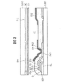
図8は本発明による液晶表示装置の他の実施例を示す構成図で、カラー表示用の各画素にそれぞれ形成されるブラックマトリクスBMのパターンを示した平面図である。
【0115】
同図において、ブラックマトリクスBMの各画素(R表示用、G表示用、B表示用の各画素)における開口をそれぞれ異なった面積としたことにある。
【0116】
カラーフィルタFILに開口(切欠き)を形成することにより、色バランス調整を図るとともに、さらに、ブラックマトリクスBMの各画素における開口によっても行わんとしていることにある。これにより、色バランスの調整の自由度が増大するようになる効果を奏する。
【0117】
本実施例は、上述した各実施例の構成を前提として構成したものであってもよく、また一部の構成を組み合わせるようにして構成してもよい。
【0118】
実施例4.
また、上述した各実施例の構成を前提とし、画素電極PXと対向電極CTとの間に電圧差がない場合に黒表示ができるいわゆるノーマリブラックモードとするようにしてもよい。
【0119】
ノーマリブラックモードはノーマリホワイトモードと比較すると液晶の層厚の不均一によっていわゆる色つきが生じやすいことが確認されている。
【0120】
上述した実施例は、透明基板SUB1の液晶側の面にて平坦化を達成でき、このことから、たとえノーマリブラックモードとしてもそれによる色つきが発生しにくいものを得ることができるようになる。
【0121】
この場合、必ずしも、カラーフィルタFILあるいはブラックマトリクスBMにおいて色バランス調整用の開口を設けなくてもよいことはいうまでもない。
【0122】
実施例5.
図9は、本発明による液晶表示装置の画素の他の実施例を示す断面図で、図3と対応した図となっている。
【0123】
透明基板SUB2側に形成されたカラーフィルタFILには開口(あるいは切欠き)が形成され、透明基板SUB1側の液晶側の面には、前記開口(あるいは切欠き)に対向する領域に該カラーフィルタFILの開口(切欠き)により生じる段差とほぼ等しい層厚の材料層を形成していることにある。
【0124】
この実施例では、該材料層を、第1画素電極PX1とソース電極SD2との間にパターン化されて形成された絶縁膜GIおよび半導体層ASの積層体によって構成している。
【0125】
このようにした場合、前記カラーフィルタFILの開口によってその部分における液晶の層厚が周囲のそれと変わってしまうのを前記材料層の形成によって回避できるようになる。
【0126】
すなわち、上述したように透明基板SUB1の液晶側の面は充分な平坦性が確保され、たとえばビーズからなるスペーサSPを介して透明基板SUB2とのギャップを確保せんとした場合に、カラーフィルタFILの開口部において、液晶の層厚が大きくなってしまうのを、透明基板SUB1側にて前記材料層からなる凸部を設けることによって防止している。
【0127】
なお、この実施例は、カラーフィルタFILが形成された透明基板SUB2の面に該カラーフィルタFILをも被って平坦化膜OCが形成された構成となっている。
【0128】
このため、平坦化膜OCの表面に顕在化されるカラーフィルタFILの開口あるいは切欠きにより生じる段差は該カラーフィルタFILの層厚よりも小さく形成されることになる。このため、前記材料層の層厚は該カラーフィルタFILの層厚よりも小さくすることができる。
【0129】
なお、この実施例において、上述した他の実施例に示した構成を合わせて適用できることはいうまでもない。
【0130】
実施例6.
図10は、本発明による液晶表示装置の画素の他の実施例を示す断面図で、図9と対応した図となっている。
【0131】
図9と比較して異なる部分は、まず、透明基板SUB2側に平坦化膜OCが形成されていない構成となっている。
【0132】
このため、カラーフィルタFILに形成された開口(切欠き)の段差は実施例5に示した場合よりも大きくなってしまう。
【0133】
そこで、透明基板SUB1側において、上述した材料層の他にゲート信号線GLを形成する際の材料をも積層させ、この積層体の合計した高さを前記開口(切欠き)の段差に合わせるようにしている。
【0134】
【発明の効果】
以上説明したことから明らかなように、本発明による液晶表示装置によれば、色バランスの調整を好適に設定し得るようになる。
【図面の簡単な説明】
【図1】本発明による液晶表示装置の画素の一実施例を示す平面図である。
【図2】本発明による液晶表示装置の一実施例を示す全体等価回路図である。
【図3】図1のIII−III線における断面図である。
【図4】本発明による液晶表示装置の各画素におけるカラーフィルタの構成の各実施例を示す平面図である。
【図5】本発明による液晶表示装置の製造方法の一実施例を示す工程図である。
【図6】本発明による液晶表示装置の画素の他の実施例を示す平面図である。
【図7】本発明による液晶表示装置の画素の他の実施例を示す平面図である。
【図8】本発明による液晶表示装置の各画素におけるブラックマトリクスの構成の一実施例を示す平面図である。
【図9】本発明による液晶表示装置の他の実施例を示す断面図である。
【図10】本発明による液晶表示装置の他の実施例を示す断面図である。
【符号の説明】
SUB1,SUB2…透明基板、GL…ゲート信号線、DL…ドレイン信号線、PX1…画素電極(透光性)、PX2…画素電極(反射電極)、TFT…薄膜トランジスタ、Cadd…容量素子、CT…対向電極。[0001]
BACKGROUND OF THE INVENTION
The present invention relates to a liquid crystal display device, and more particularly to a so-called partial transmission type active matrix liquid crystal display device.
[0002]
[Prior art]
An active matrix type liquid crystal display device includes a gate signal line extending in the x direction and arranged in parallel in the y direction on the liquid crystal side surface of one of the transparent substrates opposed to each other through the liquid crystal. And a drain signal line extending in the y direction and juxtaposed in the x direction, and a region surrounded by these signal lines is defined as a pixel region.
[0003]
In each pixel region, a thin film transistor operated by a scanning signal from a gate signal line on one side and a pixel electrode to which a video signal from a drain signal line is supplied via the thin film transistor are formed.
[0004]
Further, in such a liquid crystal display device, what is called a partially transmissive type is that each pixel region has a light transmissive portion that is a region through which light from a backlight disposed on the back side can be transmitted, the sun, etc. And a light reflecting portion which is a region where extraneous light is reflected.
[0005]
The light transmissive portion is formed as a region constituting the pixel electrode by a light transmissive conductive layer, and the light reflecting portion is formed as a region constituting the pixel electrode by a non-light transmissive conductive layer having a light reflecting function. It has become.
[0006]
The liquid crystal display device thus configured can be used as a light transmission mode by turning on a backlight, and can also be used as a light reflection mode using external light such as sunlight.
[0007]
[Problems to be solved by the invention]
However, the liquid crystal display device configured as described above must pass through the color filter twice in the light path passing through the light transmission part and the light path passing through the light reflection part, for example, in the latter case. However, in the former case, it is not configured under the same condition because it only needs to pass once.
[0008]
For this reason, it is pointed out that the color balance is not uniform between when used in the light transmission mode and when used in the light reflection mode, and it is difficult to set the color balance adjustment accordingly. It was.
[0009]
The present invention has been made based on such circumstances, and an object of the present invention is to provide a liquid crystal display device capable of suitably setting the color balance.
[0010]
[Means for Solving the Problems]
Of the inventions disclosed in this application, the outline of typical ones will be briefly described as follows.
[0011]
Means 1.
The liquid crystal display device according to the present invention includes, for example, a pixel region having a light reflecting portion and a light transmitting portion on a liquid crystal side surface of one of the substrates that are arranged to face each other through the liquid crystal. A color filter is formed in a pixel region on the liquid crystal side surface of the other substrate, and the color filter has an opening or a notch formed in a part of a portion facing the light reflecting portion.
A material layer having a thickness substantially equal to a step formed by the color filter is formed in a region facing the opening or notch of the color filter on the liquid crystal side surface of the one substrate. .
[0012]
Mean 2.
The liquid crystal display device according to the present invention includes, for example, a pixel region having a light reflection part and a light transmission part on the liquid crystal side surface of one of the substrates arranged to face each other through the liquid crystal,
A color filter is formed in a pixel region on the liquid crystal side surface of the other substrate of each of the substrates, and the color filter has a plurality of openings scattered in a portion facing the light reflecting portion. It is a feature.
[0013]
Means 3.
The liquid crystal display device according to the present invention is characterized in that, for example, the diameter of the opening is set to 20 μm or less on the premise of the configuration of the means 2.
[0014]
Means 4.
The liquid crystal display device according to the present invention includes, for example, a pixel region having a light reflection part and a light transmission part on the liquid crystal side surface of one of the substrates arranged to face each other through the liquid crystal,
Among the substrates, color filters of different colors are formed in pixel regions adjacent to each other in the pixel region on the liquid crystal side of the other substrate, and at least one color filter is a part of a portion facing the light reflecting portion. An opening or notch is formed in the
At least one of the light transmitting portions in each pixel region of the color filters of different colors is different in size from other light transmitting portions.
[0015]
Means 5.
The liquid crystal display device according to the present invention includes, for example, a pixel region having a light reflection part and a light transmission part on the liquid crystal side surface of one of the substrates arranged to face each other through the liquid crystal,
A black matrix in which an opening is provided in a portion of each substrate excluding the periphery of each pixel region on the liquid crystal side surface of the other substrate, and color filters of different colors in pixel regions adjacent to each other among the pixel regions. Formed,
In addition, at least one color filter has an opening or a notch in a part of the portion facing the light reflecting portion, and the opening of the black matrix has a color filter of a color different from the color filter color in the pixel region. It is characterized in that the size of the black matrix is different from that of other pixel regions.
[0016]
Means 6.
The liquid crystal display device according to the present invention includes, for example, a pixel region having a light reflection part and a light transmission part on the liquid crystal side surface of one of the substrates arranged to face each other through the liquid crystal,
When the intensity of the electric field generated in the pixel region is small, black display is performed,
A color filter of a different color is formed in a pixel region adjacent to each other among the pixel regions on the liquid crystal side surface of the other substrate among the substrates,
At least one of the light transmission portions in each pixel region of the different color filter is different in size from the other light transmission portions.
[0017]
Mean 7
The liquid crystal display device according to the present invention is premised on, for example, any one of means 1 to 6, and each pixel region is formed as a region surrounded by a pair of gate signal lines and a pair of drain signal lines. And a video signal from the drain signal line is supplied to the pixel electrode of the light transmission portion and the pixel electrode of the light reflection portion via the thin film transistor.
[0018]
Means 8.
The liquid crystal display device according to the present invention is characterized in that, for example, any one of the means 4, 5 and 6 is premised, and each color filter having a different color is made of cyan, magenta and yellow, respectively.
[0019]
Means 9.
The liquid crystal display device according to the present invention is premised on, for example, any one of the means 4, 5, and 6, and the area of the light reflecting portion of the pixel region where the blue color filter is formed is formed by the color filter of another color. It is characterized by being formed larger than the area of the light reflecting portion of the pixel region.
[0020]
Means 10.
The liquid crystal display device according to the present invention is premised on, for example, any one of the means 4, 5, and 6, and the area of the light reflecting portion of the pixel region where the yellow color filter is formed is formed by the color filter of another color. It is characterized in that it is formed smaller than the area of the light reflecting portion of the pixel region.
[0021]
Means 11.
The liquid crystal display device according to the present invention is characterized in that, for example, on the premise of the means 4, the total area in one pixel of the opening or notch of the color filter differs depending on the color.
[0022]
DETAILED DESCRIPTION OF THE INVENTION
Hereinafter, embodiments of a liquid crystal display device according to the present invention will be described with reference to the drawings.
[0023]
Example 1.
<Overall equivalent circuit>
FIG. 2 is a plan view showing one embodiment of the entire equivalent circuit of the liquid crystal display device according to the present invention.
[0024]
In the figure, there is a pair of transparent substrates SUB1 and SUB2 arranged to face each other via a liquid crystal, and the liquid crystal is sealed by a sealing material SL that also serves to fix the other transparent substrate SUB2 to one transparent substrate SUB1.
[0025]
On the liquid crystal side surface of the one transparent substrate SUB1 surrounded by the sealing material SL, the gate signal lines GL extending in the x direction and arranged in parallel in the y direction, and extending in the y direction and aligned in the x direction. A drain signal line DL is provided.
[0026]
A region surrounded by each gate signal line GL and each drain signal line DL constitutes a pixel region, and a matrix aggregate of these pixel regions constitutes a liquid crystal display unit AR.
[0027]
In each pixel region, a thin film transistor TFT operated by a scanning signal from one side gate signal line GL and a pixel electrode PX to which a video signal from one side drain signal line DL is supplied via the thin film transistor TFT are formed. Has been.
[0028]
The pixel electrode PX forms a capacitive element Cadd between another gate signal line GL different from the gate signal line GL for driving the thin film transistor TFT, and the capacitive element Cadd causes the pixel The video signal supplied to the electrode PX is stored for a relatively long time.
[0029]
The pixel electrode PX generates an electric field between the pixel electrode PX and the counter electrode CT formed in common in each pixel region on the other transparent substrate SUB2 side, and controls the light transmittance of the liquid crystal by this electric field. .
[0030]
One end of each of the gate signal lines GL extends beyond the sealing material SL, and the extending end constitutes a terminal to which the output terminal of the vertical scanning drive circuit V is connected. The input terminal of the vertical scanning drive circuit V receives a signal from a printed circuit board disposed outside the liquid crystal display device.
[0031]
The vertical scanning drive circuit V is composed of a plurality of semiconductor devices, and a plurality of gate signal lines GL adjacent to each other are grouped, and one semiconductor device is assigned to each group.
[0032]
Similarly, one end of each of the drain signal lines DL extends beyond the seal material SL, and the extending end constitutes a terminal to which the output terminal of the video signal driving circuit He is connected. . The input terminal of the video signal driving circuit He receives a signal from a printed circuit board arranged outside the liquid crystal display device.
[0033]
This video signal drive circuit He is also composed of a plurality of semiconductor devices, and a plurality of adjacent drain signal lines DL are grouped, and one semiconductor device is assigned to each group.
[0034]
One of the gate signal lines GL is sequentially selected by a scanning signal from the vertical scanning driving circuit V.
[0035]
Each drain signal line DL is supplied with a video signal by the video signal driving circuit He in accordance with the selection timing of the gate signal line GL.
[0036]
A backlight BL is disposed on the back surface of the liquid crystal display device configured as described above, and when the liquid crystal display device is used in a transmissive mode, the light source is turned on.
[0037]
The vertical scanning circuit V and the video signal driving circuit He are configured to be mounted on the transparent substrate SUB1, respectively. However, the present invention is not limited to this and may be externally attached to the transparent substrate SUB1. Of course it is good.
<Pixel configuration>
FIG. 1 is a plan view showing an embodiment of the pixel region. The figure shows R, G, and B pixels as color pixels, but they differ only in the color of the color filter and the proportion of the light reflecting portion and the light transmitting portion is different. The configuration is almost the same.
[0038]
In the following description, description will be given focusing on one of the three pixels. In addition, the cross section in the III-III line in the same figure is shown in FIG.
[0039]
In the figure, first, a pair of gate signal lines GL extending in the x direction and arranged in parallel in the y direction are formed on the liquid crystal side surface of the transparent substrate SUB1. The gate signal line GL is made of, for example, Al (aluminum), and an anodic oxide film AOF is formed on the surface thereof.
[0040]
These gate signal lines GL surround a rectangular region together with a pair of drain signal lines DL described later, and this region is configured as a pixel region.
[0041]
A light-transmitting pixel electrode (first pixel electrode) PX1 such as an ITO (Indium-Tin-Oxide) film is formed in the central portion excluding the slight periphery of the pixel region.
[0042]
This pixel electrode PX1 functions as a pixel electrode in a region where light from the backlight BL can transmit in the pixel region, and is distinguished from a pixel electrode (second pixel electrode) PX2 that also serves as a reflective electrode, which will be described later. is there.
[0043]
An insulating film GI made of, for example, SiN (silicon nitride) is formed on the surface of the transparent substrate SUB1 on which the gate signal line GL and the pixel electrode PX1 are thus formed. This insulating film GI is formed so as to extend over the region where the thin film transistor TFT is formed (part of the gate signal line GL) and the intersection between the gate signal line GL and the drain signal line DL in the vicinity thereof.
[0044]
The insulating film GI formed in the formation region of the thin film transistor TFT functions as a gate insulating film of the thin film transistor TFT, and the insulating film GI formed at the intersection of the gate signal line GL and the drain signal line DL serves as an interlayer insulating film. It comes to have the function of.
[0045]
A semiconductor layer AS made of amorphous Si (silicon) is formed on the surface of the insulating film.
[0046]
This semiconductor layer AS is that of the thin film transistor TFT, and by forming a drain electrode SD1 and a source electrode SD2 on the upper surface thereof, an MIS type transistor having an inverted stagger structure having a part of the gate signal line GL as a gate electrode is formed. can do.
[0047]
The semiconductor layer AS is also formed to extend at the intersection of the gate signal line GL with the drain signal line DL, thereby strengthening the function of the signal lines as an interlayer insulating film together with the insulating film GI. ing.
[0048]
Although not clarified in FIG. 3, a semiconductor layer doped with a high concentration impurity (for example, phosphorus) is formed on the surface of the semiconductor layer AS and at the interface between the drain electrode SD1 and the source electrode SD2. The contact layer d0 is constituted by this semiconductor layer.
[0049]
The drain electrode SD1 and the source electrode SD2 are formed at the same time when the drain signal line DL is formed, for example.
[0050]
That is, a drain signal line DL extending in the y direction and juxtaposed in the x direction is formed, and a part of the drain signal line DL is extended to the upper surface of the semiconductor layer AS to form the drain electrode SD1. A source electrode SD2 is formed by being separated from the electrode SD1 by the channel length of the thin film transistor TFT.
[0051]
The drain signal line DL is composed of, for example, a sequential laminate of Cr and Al.
[0052]
The source electrode SD2 extends slightly from the surface of the semiconductor layer AS to the pixel region side so as to be electrically connected to the pixel electrode PX1 and to be connected to the pixel electrode PX2 that also serves as a reflective electrode described later. The contact portion is formed.
[0053]
Here, the extending portion of the source electrode SD2 has a function of not only connecting the pixel electrodes PX1 and PX2 as described above, but also a light reflecting portion (a region where a pixel electrode PX2 described later is formed). ), The pixel electrode PX2 is formed so as to extend over most of the region of the light reflecting portion so that the height difference due to the step is not significantly increased.
[0054]
That is, when the extension part of the source electrode SD2 is only provided with a function of connecting the pixel electrodes PX1 and PX2, the extension part may be formed as a contact part, and the extension part is relatively It will be short. As a result, a step around the extended portion becomes apparent on the surface (upper surface of a protective film PSV described later) on which a pixel electrode PX2 also serving as a later-described reflective electrode is formed, and a step is also formed on the surface of the pixel electrode PX2. Will be.
[0055]
Further, by adopting the configuration as in this embodiment, the extended portion of the source electrode SD2 occupies a relatively large area, which means that the side becomes relatively long.
[0056]
For this reason, in the manufacture of the liquid crystal display device, impurities such as dust are less likely to remain in the vicinity of the pixel electrode PX2, and harmful effects due to the impurities can be removed.
[0057]
Incidentally, in the case of a source electrode of a thin film transistor TFT having a function as a contact portion, the area of the contact portion is small, and its side is also slightly complicated by selective etching by photolithography technology, and impurities such as dust remain there. In many cases, the function as the contact portion is impaired.
[0058]
A protective film PSV made of, for example, SiN is formed on the surface of the transparent substrate SUB1 on which the drain signal line DL, the drain electrode SD1 and the source electrode SD2 of the thin film transistor TFT are thus formed. This protective film PSV is a layer that avoids direct contact with the liquid crystal of the thin film transistor TFT, and is intended to prevent deterioration of characteristics of the thin film transistor TFT.
[0059]
Further, a contact hole CH is formed in the protective film PSV, and a part of the source electrode SD2 of the thin film transistor TFT is exposed in the contact hole CH.
[0060]
A pixel electrode PX2 that also serves as a reflective electrode is formed on the upper surface of the protective film. This pixel electrode is composed of a non-translucent conductive film made of a sequential laminate of, for example, Cr and Al.
[0061]
The pixel electrode PX2 is formed so as to occupy most of the pixel region while avoiding the region serving as the light transmission part.
[0062]
Thereby, the region where the pixel electrode PX2 is formed functions as a light reflecting portion in the pixel region, and the formation region of the pixel electrode PX1 exposed (viewed in a plan view) from the pixel electrode PX2 functions as a light transmitting portion. It is supposed to be.
[0063]
In this embodiment, the area occupied by the light transmitting portion of the pixel region in charge of blue (B) is formed smaller than the area occupied by the light transmitting portion of the pixel region in charge of other colors (R, G). Yes. In other words, the area of the second pixel electrode PX2 in the pixel area responsible for blue is formed larger than the area of the first pixel electrode PX2 in the pixel area responsible for other colors.
[0064]
The reason for this is that the amount of light from the backlight irradiated through the light transmission part is suitable for mixing the three primary colors when it is blue, and the ratio of the light transmission part to the light reflection part of this light quantity is It is because it becomes more suitable by setting appropriately.
[0065]
A part of the pixel electrode PX2 is electrically connected to the source electrode SD2 of the thin film transistor TFT through a contact hole CH formed in a part of the protective film PSV.
[0066]
Further, the pixel electrode PX2 is formed to extend until it overlaps with another adjacent gate signal line GL different from the gate signal line GL for driving the thin film transistor TFT, and the protective film PSV is formed as a dielectric in this portion. A capacitor element Cadd serving as a body film is formed.
[0067]
Thus, an alignment film (not shown) is formed on the upper surface of the transparent substrate SUB1 on which the pixel electrode PX2 is formed so as to cover the pixel electrode PX2 and the like. This alignment film is in direct contact with the liquid crystal LC, and the initial alignment direction of the molecules of the liquid crystal is determined by rubbing formed on the surface thereof.
[0068]
The transparent substrate SUB2 is disposed opposite to the transparent substrate SUB1 thus configured via the liquid crystal LC, and the black matrix BM is formed on the surface of the transparent substrate SUB2 on the liquid crystal side so as to define each pixel region. Is formed. That is, at least the black matrix BM formed in the liquid crystal display portion AR has a pattern in which openings are formed in the regions that leave the periphery of each pixel region, thereby improving the display contrast.
[0069]
Further, the black matrix BM is formed so as to sufficiently cover the thin film transistor TFT on the transparent substrate SUB1 side, and prevents deterioration of characteristics of the thin film transistor TFT by preventing the irradiation of the external light to the thin film transistor TFT. Yes. The black matrix BM is composed of a resin film containing a black pigment, for example.
[0070]
A color filter FIL is formed on the surface of the transparent substrate SUB2 on which the black matrix BM is formed, covering the opening of the black matrix BM. This color filter is made up of, for example, red (R), green (G), and blue (B) color filters. For example, a red filter is commonly formed in each pixel region group arranged in the y direction. It is formed in an array such as a red (R) color, a green (G) color, a blue (B) color, a red (R) color,. Yes. Each of these filters is composed of a resin film containing a pigment corresponding to the color. Needless to say, the color of each filter may be cyan, magenta, or yellow.
[0071]
Here, in this embodiment, the color filter FIL is formed in a part of the pixel region, and for example, as shown in FIG. 4A, it is formed in the central portion excluding the left and right of the pixel region. ing. In other words, an opening (or notch) HL is formed at a portion facing a part of the second pixel electrode PX2 (left and right of the pixel region).
[0072]
The reason why the color filter FIL is configured as described above is that the brightness of each pixel at the time of reflection can be adjusted from the viewpoint of mixing the three primary colors. Thereby, even if it is a case where it cannot adjust only by changing the area ratio of a light transmission part and a light reflection part with a color, a color balance and brightness can be adjusted, and a freedom degree increases. Furthermore, the area of the opening HL may be different from the area of the opening HL of the color filter FIL of the pixel region in charge of another adjacent color.
[0073]
In this case, it has been confirmed that the color adjustment can be easily performed by setting the opening HL of the blue color filter FIL to be smaller than the openings HL of the color filters FIL of other colors. Therefore, as another embodiment, the openings HL may be provided in the color filters FIL of other colors without providing the openings HL of the blue color filter FIL.
[0074]
When the color filter FIL is configured in this way, it is possible to adjust the color balance, and as described above, the area of the light transmitting portion of the pixel region in charge of blue is the same as that of the pixel region in charge of other colors. For example, the area of the light transmission part of the pixel region in charge of other colors can be made the same without making it smaller than the area of the light transmission part.
[0075]
Although the provision of the opening HL in the color filter FIL in this way prevents the liquid crystal LC from having a uniform thickness, the step is sufficiently eliminated on the transparent substrate SUB1 side as described above. Therefore, it can be suppressed to a range where there is virtually no harmful effect.
[0076]
A flattening film OC is formed on the surface of the transparent substrate SUB2 on which the black matrix BM and the color filter FIL are formed so as to cover the black matrix BM and the color filter FIL. The planarization film OC is made of a resin film that can be formed by coating, and is provided to reduce the level difference that becomes apparent due to the formation of the black matrix BM and the color filter FIL.
[0077]
A translucent conductive film made of, for example, an ITO film is formed on the upper surface of the planarizing film OC, and a common counter electrode CT is formed in each pixel region by this conductive film.
[0078]
An alignment film (not shown) is formed on the surface of the planarizing film OC, and this alignment film is in direct contact with the liquid crystal LC, and the initial alignment direction of the molecules of the liquid crystal by rubbing formed on the surface. Is supposed to determine.
[0079]
The liquid crystal display device thus formed is formed by extending the source electrode SD2 of the thin film transistor TFT over a region corresponding to the light reflecting portion of the pixel region.
[0080]
For this reason, the pixel electrode PX2 formed on the light reflecting portion via the protective film PSV is formed in a flat shape having no height difference due to a step.
[0081]
This means that the layer thickness of the liquid crystal becomes uniform in the light reflecting portion, and the reduction in contrast caused by this variation can be greatly suppressed.
[0082]
Although not a light reflecting portion, the height of the pixel electrode PX2 with respect to the transparent substrate SUB1 in the portion where the capacitive element Cadd is formed should be substantially equal to the height of the pixel electrode PX2 with respect to the transparent substrate SUB1 in the light reflecting portion. Can do.
[0083]
The portion where the capacitive element Cadd is formed is a portion covered with the black matrix BM. In the portion close to the capacitive element Cadd in the opening of the black matrix BM, the transparent substrate SUB1 of the pixel electrode PX2 is formed. It is possible to prevent the influence due to the difference in height with respect to.
[0084]
Therefore, the difference between the layer thickness of the gate signal line GL, which is the portion of the capacitive element Cadd, and the total layer thickness of the pixel electrode PX1 and the source electrode SD2 of the thin film transistor TFT under the reflecting portion is set to 0.1 μm or less. As a result, the height variation of the pixel electrode PX2 with respect to the transparent substrate SUB1 can be set to 0.1 μm or less.
[0085]
As a result, the layer thickness of the liquid crystal LC can be made substantially uniform in the light reflecting portion of the pixel region, and thus the reduction in contrast can be suppressed.
[0086]
In the above-described embodiment, the source electrode SD2 of the thin film transistor TFT is sufficiently extended to the region of the light reflecting portion, thereby avoiding the generation of a step in the pixel electrode PX2 formed thereabove.
[0087]
However, it goes without saying that the same effect as described above may be brought about by using another material layer electrically (or physically) separated from the source electrode SD2.
[0088]
In this case, since the film thickness of the material layer can be set regardless of the source electrode SD2 of the thin film transistor TFT, there is an effect that the pixel electrode PX2 can be easily flattened.
[0089]
In the above-described embodiment, the color filter FIL is provided with the opening (notch) HL in the left and right portions of the pixel region and facing the second pixel electrode PX2. As shown in FIG. 4B, it goes without saying that openings may be formed in the upper and lower portions of the pixel region and in the portion facing the second pixel electrode PX2. Further, as shown in FIG. 4C, it is a matter of course that an opening having a relatively large area may be provided in a substantially central portion of the pixel region. Furthermore, as shown in FIG. 4D, it is needless to say that a plurality of small openings having a diameter of 20 μm or less, for example, scattered in the substantially central portion of the pixel region may be formed.
[0090]
With the configuration shown in FIG. 4D, the influence of the step due to the opening of the color filter FIL can be reduced, and thereby the liquid crystal layer thickness can be made uniform.
[0091]
In this case, as described above, in each color filter FIL, for example, the area of the opening of the blue color filter FIL may be reduced and the opening may not be formed.
"Production method"
Hereinafter, an example of a manufacturing method of the configuration on the transparent substrate SUB1 side in the above-described liquid crystal display device will be described with reference to FIG.
[0092]
Step 1. (Fig. 5 (a))
A transparent substrate SUB1 is prepared, and Al is formed with a film thickness of about 300 nm on the main surface (surface on the liquid crystal side) by sputtering, for example, and this is selectively etched by photolithography to form gate signal lines GL. As the etchant, for example, a mixed solution of phosphoric acid, hydrochloric acid, and nitric acid is used.
[0093]
Then, the gate signal line GL is anodized in a tartaric acid solution to form an anodized film AOF on the surface thereof. An appropriate film thickness of the anodic oxide film AOF is about 180 nm.
[0094]
Step 2. (Fig. 5 (b))
A transparent conductive film made of, for example, an ITO (Indium-Tin-Oxide) film is formed on the main surface of the transparent substrate SUB1 on which the gate signal line GL is formed with a film thickness of about 100 nm, and this is selected by photolithography technology. Etching is performed to form the pixel electrode PX1. For example, an aqua regia solution is used as the etchant.
[0095]
Step 3. (Fig. 5 (c))
An insulating film made of SiN is formed with a film thickness of about 240 nm on the main surface of the transparent substrate SUB1 on which the pixel electrode PX1 is formed, for example, by a CVD method. Then, after forming an amorphous silicon layer with a film thickness of about 200 nm by the same method, further, n doped with phosphorus (P) + A type amorphous silicon layer is formed with a film thickness of about 35 nm.
[0096]
Then, selective etching by a photolithography technique is performed, and the semiconductor layer and the insulating film are collectively etched to form the insulating film GI and the semiconductor layer AS. As the etching in this case, dry etching using sulfur hexafluoride gas is appropriate.
[0097]
In this case, since the etching rate of amorphous silicon is higher than that of the insulating film, a forward taper of about 4 ° is formed on the side forming the outline of the semiconductor layer AS. Thus, a forward taper of about 70 ° is formed.
[0098]
Step 4. (Fig. 5 (d))
A Cr layer and an Al layer are sequentially formed on the main surface of the transparent substrate SUB1 on which the insulating film GI and the semiconductor layer AS are formed, for example, by sputtering. In this case, it is appropriate that the Cr layer has a thickness of 30 nm and the Al layer has a thickness of 200 nm.
[0099]
Thereafter, selective etching by photolithography is performed to form a drain signal line DL having a two-layer structure, a drain electrode SD1 and a source electrode SD2 of the thin film transistor TFT.
[0100]
In this case, a mixed solution of phosphoric acid, hydrochloric acid and nitric acid is suitable as the Al etching solution, and a ceric ammonium nitrate solution is suitable as the Cr etching solution.
[0101]
Then, using the drain electrode SD1 and the source electrode SD2 of the patterned thin film transistor TFT as a mask, n on the surface of the semiconductor layer AS exposed therefrom + The amorphous silicon layer of the mold is etched. As an etchant in this case, dry etching using sulfur hexafluoride gas is appropriate.
[0102]
Step 5. (Fig. 5 (e))
On the main surface of the transparent substrate SUB1 on which the drain signal line DL, the drain electrode SD1 and the source electrode SD2 of the thin film transistor TFT are formed, SiN is formed with a film thickness of about 600 nm by using, for example, a CVD method, and this is selected by photolithography technology. Etching is performed to form the protective film PSV.
[0103]
In this etching, a contact hole CH for exposing a part of the extending portion of the source electrode SD2 of the thin film transistor TFT is formed at the same time.
[0104]
Step 6. (Fig. 5 (f))
A Cr layer with a layer thickness of about 30 nm and an Al layer with a layer thickness of about 200 nm are sequentially formed on the main surface of the transparent substrate SUB1 on which the protective film PSV is formed by using, for example, a sputtering method. Etching is performed to form a pixel electrode PX2 that also serves as a reflective electrode.
[0105]
In this case, a mixed solution of phosphoric acid, hydrochloric acid and nitric acid is suitable as the Al etching solution, and a ceric ammonium nitrate solution is suitable as the Cr etching solution.
[0106]
In this case, the pixel electrode PX2 has an opening so as to occupy about half of the pixel area.
[0107]
Note that, instead of sequentially forming the Cr layer and the Al layer as the pixel electrode PX2, a Mo alloy and Al may be sequentially formed, or a Mo alloy and an Al alloy may be sequentially formed. As the Mo alloy, MoCr is preferable. In this case, it has the effect that it can etch at once.
[0108]
Example 2
6 (a) to 6 (e), 7 (a) and 7 (b) are configuration diagrams showing other embodiments of the liquid crystal display device according to the present invention, and correspond to FIG.
[0109]
FIG. 6A shows a configuration in which the second protective film PSV2 is formed on the upper surface of the pixel electrode PX2 so as to cover the pixel electrode PX2. FIG. 6B shows a configuration in which an opening is formed in the protective film PSV in a region corresponding to the light transmission portion. FIG. 6C shows a configuration in which the second protective film PSV2 is formed on the upper surface of the pixel electrode PX2 so as to cover the pixel electrode PX2, and both the protective film PSV and the second protective film PSV2 transmit light. The opening is formed in the region corresponding to the part. FIG. 6D shows a configuration in which the second protective film PSV2 is formed on the upper surface of the pixel electrode PX2 so as to cover the pixel electrode PX2, and an opening is formed only in the protective film PSV in a region corresponding to the light transmission portion. It is set as the formed structure. FIG. 6E shows a configuration in which the second protective film PSV2 is formed on the upper surface of the pixel electrode PX2 so as to cover the pixel electrode PX2, and both the protective film PSV and the second protective film PSV2 transmit light. In the region corresponding to the portion, openings are collectively formed.
[0110]
FIG. 7A shows the gate electrode GL formed of a metal other than the Al layer whose surface is anodized, for example, composed of an alloy layer of Mo and Cr.
[0111]
Further, in FIG. 7B, the part different from the case of FIG. 3 is that a material layer DML for height adjustment is formed in the part where the light reflecting part and the capacitive element Cadd are formed.
[0112]
Thereby, the height difference of each pixel electrode PX2 with respect to the transparent substrate SUB1 can be set to 0.1 μm or less in each of those portions.
[0113]
Therefore, the material layer DML for height adjustment need not be formed in each of the portions where the light reflecting portion and the capacitive element Cadd are formed, as shown in FIG. Of course, it may be formed.
[0114]
Example 3 FIG.
FIG. 8 is a block diagram showing another embodiment of the liquid crystal display device according to the present invention, and is a plan view showing a pattern of a black matrix BM formed in each pixel for color display.
[0115]
In the figure, the openings in the respective pixels (R display pixels, G display pixels, and B display pixels) of the black matrix BM have different areas.
[0116]
By forming an opening (notch) in the color filter FIL, the color balance is adjusted, and further, the opening is made in each pixel of the black matrix BM. Thereby, there is an effect that the degree of freedom in adjusting the color balance is increased.
[0117]
The present embodiment may be configured based on the configuration of each of the above-described embodiments, or may be configured by combining some configurations.
[0118]
Example 4
Further, on the premise of the configuration of each embodiment described above, a so-called normally black mode in which black display is possible when there is no voltage difference between the pixel electrode PX and the counter electrode CT may be employed.
[0119]
It has been confirmed that the normally black mode is more likely to be colored due to the non-uniformity of the liquid crystal layer thickness compared to the normally white mode.
[0120]
In the embodiment described above, flattening can be achieved on the surface of the transparent substrate SUB1 on the liquid crystal side, and from this, even in the normally black mode, it is possible to obtain one that hardly causes coloring. .
[0121]
In this case, needless to say, it is not always necessary to provide a color balance adjustment opening in the color filter FIL or the black matrix BM.
[0122]
Embodiment 5 FIG.
FIG. 9 is a sectional view showing another embodiment of the pixel of the liquid crystal display device according to the present invention and corresponds to FIG.
[0123]
An opening (or notch) is formed in the color filter FIL formed on the transparent substrate SUB2 side, and the color filter is provided in a region facing the opening (or notch) on the liquid crystal side surface on the transparent substrate SUB1 side. That is, a material layer having a layer thickness substantially equal to a step generated by the opening (notch) of the FIL is formed.
[0124]
In this embodiment, the material layer is constituted by a stacked body of an insulating film GI and a semiconductor layer AS formed by patterning between the first pixel electrode PX1 and the source electrode SD2.
[0125]
In this case, the formation of the material layer can prevent the thickness of the liquid crystal layer from changing due to the opening of the color filter FIL.
[0126]
That is, as described above, the liquid crystal side surface of the transparent substrate SUB1 is sufficiently flat. For example, when the gap with the transparent substrate SUB2 is not secured through the spacer SP made of beads, the color filter FIL In the opening, the liquid crystal layer thickness is prevented from being increased by providing a convex portion made of the material layer on the transparent substrate SUB1 side.
[0127]
In this embodiment, the planarizing film OC is formed on the surface of the transparent substrate SUB2 on which the color filter FIL is formed so as to cover the color filter FIL.
[0128]
For this reason, the level difference caused by the opening or notch of the color filter FIL that appears on the surface of the planarizing film OC is formed smaller than the layer thickness of the color filter FIL. For this reason, the layer thickness of the material layer can be made smaller than the layer thickness of the color filter FIL.
[0129]
In this embodiment, it goes without saying that the configurations shown in the other embodiments described above can be applied together.
[0130]
Example 6
FIG. 10 is a sectional view showing another embodiment of the pixel of the liquid crystal display device according to the present invention and corresponds to FIG.
[0131]
The difference from FIG. 9 is that the planarizing film OC is not formed on the transparent substrate SUB2 side.
[0132]
For this reason, the level | step difference of the opening (notch) formed in the color filter FIL will become larger than the case where it shows in Example 5. FIG.
[0133]
Therefore, on the transparent substrate SUB1 side, a material for forming the gate signal line GL is stacked in addition to the above-described material layer, and the total height of the stacked body is adjusted to the step of the opening (notch). I have to.
[0134]
【The invention's effect】
As is apparent from the above description, according to the liquid crystal display device of the present invention, the color balance can be adjusted appropriately.
[Brief description of the drawings]
FIG. 1 is a plan view showing one embodiment of a pixel of a liquid crystal display device according to the present invention.
FIG. 2 is an overall equivalent circuit diagram showing an embodiment of a liquid crystal display device according to the present invention.
3 is a cross-sectional view taken along line III-III in FIG.
FIG. 4 is a plan view showing each embodiment of the configuration of a color filter in each pixel of the liquid crystal display device according to the present invention.
FIG. 5 is a process diagram showing an embodiment of a method of manufacturing a liquid crystal display device according to the present invention.
FIG. 6 is a plan view showing another embodiment of the pixel of the liquid crystal display device according to the present invention.
FIG. 7 is a plan view showing another embodiment of the pixel of the liquid crystal display device according to the present invention.
FIG. 8 is a plan view showing one embodiment of the configuration of a black matrix in each pixel of the liquid crystal display device according to the present invention.
FIG. 9 is a cross-sectional view showing another embodiment of the liquid crystal display device according to the present invention.
FIG. 10 is a cross-sectional view showing another embodiment of the liquid crystal display device according to the present invention.
[Explanation of symbols]
SUB1, SUB2 ... transparent substrate, GL ... gate signal line, DL ... drain signal line, PX1 ... pixel electrode (translucent), PX2 ... pixel electrode (reflection electrode), TFT ... thin film transistor, Cadd ... capacitor element, CT ... opposite electrode.
Claims (5)
前記第1の基板と前記第2の基板との間に設けられ、1つの画素内に、光反射部と、光透過部と、カラーフィルタとを有する複数の画素とを備えた液晶表示装置であって、
前記カラーフィルタは、前記1つの画素内に径が20μm以下の複数の円形の開口を有し、前記カラーフィルタの前記開口は前記光反射部に対向する部分に形成されており、
前記カラーフィルタの前記開口によって形成される段差を平坦化する平坦化膜が、前記カラーフィルタを覆って形成されていることを特徴とする液晶表示装置。A first substrate and a second substrate that are arranged opposite to each other with a liquid crystal interposed therebetween;
A liquid crystal display device provided between the first substrate and the second substrate, wherein the pixel includes a plurality of pixels each having a light reflection portion, a light transmission portion, and a color filter in one pixel. There,
The color filter, the have diameters within one pixel the following plurality of circular openings 20 [mu] m, the opening of the color filter is formed in a portion opposed to the light reflecting portion,
A liquid crystal display device , wherein a flattening film for flattening a step formed by the opening of the color filter is formed so as to cover the color filter .
前記画素電極は、前記光透過部に開口を有することを特徴とする請求項1に記載の液晶表示装置。The pixel has a pixel electrode that reflects light in the light reflecting portion;
The liquid crystal display device according to claim 1, wherein the pixel electrode has an opening in the light transmission portion.
前記第2の基板は、前記カラーフィルタを有することを特徴とする請求項2に記載の液晶表示装置。The first substrate has the pixel electrode,
The liquid crystal display device according to claim 2 , wherein the second substrate includes the color filter.
Priority Applications (9)
| Application Number | Priority Date | Filing Date | Title |
|---|---|---|---|
| JP2001148812A JP4398602B2 (en) | 2001-05-18 | 2001-05-18 | Liquid crystal display |
| TW091105084A TW584766B (en) | 2001-05-18 | 2002-03-18 | Liquid crystal display device |
| US10/107,928 US7750996B2 (en) | 2001-05-18 | 2002-03-26 | Liquid crystal display device |
| KR1020020025611A KR100642372B1 (en) | 2001-05-18 | 2002-05-09 | Liquid crystal display device |
| CNB2004101011438A CN100347595C (en) | 2001-05-18 | 2002-05-17 | Liquid crystal display device |
| CNB021198969A CN1209671C (en) | 2001-05-18 | 2002-05-17 | Liquid crystal display device |
| CNB2005100813385A CN100381909C (en) | 2001-05-18 | 2002-05-17 | Liquid crystal display device |
| KR1020050049362A KR20050069957A (en) | 2001-05-18 | 2005-06-09 | Liquid crystal display device |
| US12/660,871 US7995173B2 (en) | 2001-05-18 | 2010-03-05 | Liquid crystal display device |
Applications Claiming Priority (1)
| Application Number | Priority Date | Filing Date | Title |
|---|---|---|---|
| JP2001148812A JP4398602B2 (en) | 2001-05-18 | 2001-05-18 | Liquid crystal display |
Related Child Applications (1)
| Application Number | Title | Priority Date | Filing Date |
|---|---|---|---|
| JP2007234112A Division JP4398999B2 (en) | 2007-09-10 | 2007-09-10 | Liquid crystal display |
Publications (3)
| Publication Number | Publication Date |
|---|---|
| JP2002341335A JP2002341335A (en) | 2002-11-27 |
| JP2002341335A5 JP2002341335A5 (en) | 2005-10-13 |
| JP4398602B2 true JP4398602B2 (en) | 2010-01-13 |
Family
ID=18994062
Family Applications (1)
| Application Number | Title | Priority Date | Filing Date |
|---|---|---|---|
| JP2001148812A Expired - Fee Related JP4398602B2 (en) | 2001-05-18 | 2001-05-18 | Liquid crystal display |
Country Status (5)
| Country | Link |
|---|---|
| US (2) | US7750996B2 (en) |
| JP (1) | JP4398602B2 (en) |
| KR (2) | KR100642372B1 (en) |
| CN (3) | CN100381909C (en) |
| TW (1) | TW584766B (en) |
Families Citing this family (40)
| Publication number | Priority date | Publication date | Assignee | Title |
|---|---|---|---|---|
| KR100483358B1 (en) * | 2001-09-07 | 2005-04-14 | 엘지.필립스 엘시디 주식회사 | method for fabricating a Transflective liquid crystal display device and the same |
| JP4200830B2 (en) * | 2002-10-11 | 2008-12-24 | セイコーエプソン株式会社 | Electro-optical device manufacturing method, electro-optical device, and electronic apparatus |
| TW594230B (en) * | 2002-11-12 | 2004-06-21 | Prime View Int Co Ltd | Reflective plate of reflective-type liquid crystal display and method for producing the same |
| KR100907479B1 (en) * | 2002-12-31 | 2009-07-13 | 삼성전자주식회사 | Color filter substrate and liquid crystal display having the same |
| JP3918765B2 (en) | 2003-04-21 | 2007-05-23 | セイコーエプソン株式会社 | Liquid crystal display device and electronic device |
| KR100494455B1 (en) * | 2003-06-11 | 2005-06-10 | 엘지.필립스 엘시디 주식회사 | An array substrate for transflective LCD and method for fabricating of the same |
| KR101007719B1 (en) * | 2003-07-31 | 2011-01-13 | 삼성전자주식회사 | Color filter substrate and liquid crystal display apparatus having the same |
| JP4461748B2 (en) * | 2003-09-11 | 2010-05-12 | ソニー株式会社 | Liquid crystal display device and manufacturing method thereof |
| JP2005114966A (en) * | 2003-10-07 | 2005-04-28 | Alps Electric Co Ltd | Color liquid crystal display |
| US7495722B2 (en) | 2003-12-15 | 2009-02-24 | Genoa Color Technologies Ltd. | Multi-color liquid crystal display |
| CN103177701A (en) * | 2003-12-15 | 2013-06-26 | 格诺色彩技术有限公司 | Multi-primary liquid crystal display |
| CN100359376C (en) * | 2004-02-24 | 2008-01-02 | 统宝光电股份有限公司 | Semitransparent-half reflection type LCD |
| JP4111180B2 (en) * | 2004-09-02 | 2008-07-02 | セイコーエプソン株式会社 | Liquid crystal display device and electronic device |
| JP4158763B2 (en) * | 2004-12-01 | 2008-10-01 | セイコーエプソン株式会社 | Liquid crystal display device, method for manufacturing liquid crystal display device, and electronic apparatus |
| KR101125248B1 (en) * | 2004-12-23 | 2012-03-21 | 엘지디스플레이 주식회사 | Color Filter Substrate of Transflective Type And Fabricating Method Thereof |
| KR101107270B1 (en) * | 2004-12-31 | 2012-01-19 | 엘지디스플레이 주식회사 | Thin Film Transistor Substrate And Fabricating Method Thereof, Liquid Crystal Display Panel Using The Same And Fabricating Method Thereof |
| JP2006330243A (en) * | 2005-05-25 | 2006-12-07 | Optrex Corp | Translucent color liquid crystal display apparatus |
| JP2006330602A (en) * | 2005-05-30 | 2006-12-07 | Sharp Corp | Liquid crystal display device and its manufacturing method |
| JP2007003778A (en) * | 2005-06-23 | 2007-01-11 | Mitsubishi Electric Corp | Transflective liquid crystal display device and method for manufacturing the same |
| JP3974141B2 (en) * | 2005-06-23 | 2007-09-12 | 三菱電機株式会社 | Transflective liquid crystal display device |
| KR20070000123A (en) * | 2005-06-27 | 2007-01-02 | 엘지.필립스 엘시디 주식회사 | Transflective lcd and method for fabricating of the same |
| JP4950480B2 (en) * | 2005-11-22 | 2012-06-13 | 東芝モバイルディスプレイ株式会社 | Liquid crystal display |
| CN100371794C (en) * | 2005-12-22 | 2008-02-27 | 友达光电股份有限公司 | Color filter |
| JP4572837B2 (en) * | 2006-02-01 | 2010-11-04 | ソニー株式会社 | Liquid crystal device and electronic device |
| KR20070084851A (en) | 2006-02-22 | 2007-08-27 | 삼성전자주식회사 | Transflective liquid crystal display and panel therefor |
| JP4404072B2 (en) * | 2006-06-21 | 2010-01-27 | エプソンイメージングデバイス株式会社 | LCD panel |
| KR100893488B1 (en) * | 2008-02-28 | 2009-04-17 | 삼성모바일디스플레이주식회사 | Liquid crystal display device |
| JP4900318B2 (en) * | 2008-05-13 | 2012-03-21 | セイコーエプソン株式会社 | Liquid crystal display device and electronic device |
| JP5389529B2 (en) * | 2009-05-20 | 2014-01-15 | 株式会社ジャパンディスプレイ | Liquid crystal display device and manufacturing method thereof |
| JP6147953B2 (en) | 2011-03-15 | 2017-06-14 | 株式会社ジャパンディスプレイ | Display device |
| US8913093B2 (en) * | 2011-09-30 | 2014-12-16 | Lg Display Co., Ltd. | Liquid crystal display device |
| KR101490467B1 (en) * | 2011-09-30 | 2015-02-06 | 엘지디스플레이 주식회사 | Liquid crystal display device |
| TWI463193B (en) * | 2011-11-17 | 2014-12-01 | Au Optronics Corp | Color filter and liquid crystal display |
| KR20130116092A (en) * | 2012-04-12 | 2013-10-23 | 삼성디스플레이 주식회사 | Display apparatus |
| CN102736314B (en) * | 2012-06-29 | 2015-03-25 | 京东方科技集团股份有限公司 | Liquid crystal panel and manufacturing method thereof as well as liquid crystal display |
| CN104375319B (en) | 2014-12-01 | 2017-07-25 | 京东方科技集团股份有限公司 | Black matrix structure and preparation method, array base palte, color membrane substrates and display device |
| CN105093669B (en) * | 2015-10-09 | 2018-09-25 | 京东方科技集团股份有限公司 | A kind of color membrane substrates and preparation method thereof, display panel, display device |
| CN110828485B (en) * | 2019-11-19 | 2022-08-26 | 京东方科技集团股份有限公司 | Display substrate, preparation method thereof and display device |
| CN113451488B (en) * | 2020-05-27 | 2022-11-11 | 重庆康佳光电技术研究院有限公司 | Display device and method of manufacturing the same |
| CN114005865B (en) * | 2021-12-30 | 2022-03-22 | 北京京东方技术开发有限公司 | Display substrate, preparation method thereof and electronic device |
Family Cites Families (23)
| Publication number | Priority date | Publication date | Assignee | Title |
|---|---|---|---|---|
| US5122891A (en) * | 1986-12-29 | 1992-06-16 | Goldstar Co., Ltd. | Color liquid crystal display device |
| JP3350991B2 (en) * | 1992-03-06 | 2002-11-25 | セイコーエプソン株式会社 | Electro-optical device substrate and electro-optical device |
| JP3881092B2 (en) * | 1997-07-10 | 2007-02-14 | シチズン時計株式会社 | LCD panel |
| US5936694A (en) | 1995-04-26 | 1999-08-10 | Canon Kabushiki Kaisha | Liquid crystal device and process for producing same |
| JP2001133768A (en) | 1995-04-26 | 2001-05-18 | Canon Inc | Method of producing liquid crystal device, and liquid crystal device |
| KR19990072175A (en) * | 1996-10-17 | 1999-09-27 | 요트.게.아. 롤페즈 | Color display device with color-filter layers |
| US6124909A (en) | 1996-12-25 | 2000-09-26 | Casio Computer Co., Ltd. | Color liquid crystal display device having a plurality of pixel areas which emit non-colored light |
| JPH10319386A (en) | 1997-05-16 | 1998-12-04 | Casio Comput Co Ltd | Liquid crystal display panel |
| JP3738549B2 (en) | 1997-12-22 | 2006-01-25 | カシオ計算機株式会社 | Liquid crystal display element |
| JPH11183891A (en) | 1997-12-22 | 1999-07-09 | Casio Comput Co Ltd | Liquid crystal display element |
| US6624860B1 (en) * | 1998-01-26 | 2003-09-23 | Sharp Kabushiki Kaisha | Color filter layer providing transmitted light with improved brightness and display device using same |
| JP3335130B2 (en) | 1998-01-26 | 2002-10-15 | シャープ株式会社 | Liquid crystal display |
| US6215538B1 (en) | 1998-01-26 | 2001-04-10 | Sharp Kabushiki Kaisha | Liquid crystal display including both color filter and non-color filter regions for increasing brightness |
| WO1999040480A1 (en) * | 1998-02-04 | 1999-08-12 | Seiko Epson Corporation | Liquid crystal display and electronic device |
| JPH11326625A (en) * | 1998-05-13 | 1999-11-26 | Seiko Epson Corp | Color filter, color liquid crystal display, and production thereof |
| JP3237632B2 (en) * | 1998-11-30 | 2001-12-10 | カシオ計算機株式会社 | Liquid crystal display |
| JP2000241808A (en) | 1999-02-18 | 2000-09-08 | Seiko Instruments Inc | Liquid crystal display element |
| JP2000330103A (en) * | 1999-05-14 | 2000-11-30 | Koninkl Philips Electronics Nv | Reflection liquid crystal display device |
| JP2001033782A (en) * | 1999-07-16 | 2001-02-09 | Advanced Display Inc | Liquid crystal display device |
| JP2001117086A (en) * | 1999-10-15 | 2001-04-27 | Toshiba Corp | Liquid crystal display device |
| JP2001133766A (en) | 2000-08-29 | 2001-05-18 | Semiconductor Energy Lab Co Ltd | Liquid crystal display device |
| JP3941481B2 (en) * | 2000-12-22 | 2007-07-04 | セイコーエプソン株式会社 | Liquid crystal display device and electronic device |
| US6501521B2 (en) * | 2001-03-07 | 2002-12-31 | Sharp Kabushiki Kaisha | Transmission/reflection type color liquid crystal display device |
-
2001
- 2001-05-18 JP JP2001148812A patent/JP4398602B2/en not_active Expired - Fee Related
-
2002
- 2002-03-18 TW TW091105084A patent/TW584766B/en not_active IP Right Cessation
- 2002-03-26 US US10/107,928 patent/US7750996B2/en not_active Expired - Fee Related
- 2002-05-09 KR KR1020020025611A patent/KR100642372B1/en active IP Right Grant
- 2002-05-17 CN CNB2005100813385A patent/CN100381909C/en not_active Expired - Fee Related
- 2002-05-17 CN CNB2004101011438A patent/CN100347595C/en not_active Expired - Fee Related
- 2002-05-17 CN CNB021198969A patent/CN1209671C/en not_active Expired - Fee Related
-
2005
- 2005-06-09 KR KR1020050049362A patent/KR20050069957A/en not_active Application Discontinuation
-
2010
- 2010-03-05 US US12/660,871 patent/US7995173B2/en not_active Expired - Fee Related
Also Published As
| Publication number | Publication date |
|---|---|
| CN100381909C (en) | 2008-04-16 |
| CN100347595C (en) | 2007-11-07 |
| TW584766B (en) | 2004-04-21 |
| US7750996B2 (en) | 2010-07-06 |
| US20100171911A1 (en) | 2010-07-08 |
| KR100642372B1 (en) | 2006-11-03 |
| US20020171791A1 (en) | 2002-11-21 |
| CN1209671C (en) | 2005-07-06 |
| US7995173B2 (en) | 2011-08-09 |
| CN1387074A (en) | 2002-12-25 |
| JP2002341335A (en) | 2002-11-27 |
| KR20050069957A (en) | 2005-07-05 |
| CN1696797A (en) | 2005-11-16 |
| CN1619386A (en) | 2005-05-25 |
| KR20020088354A (en) | 2002-11-27 |
Similar Documents
| Publication | Publication Date | Title |
|---|---|---|
| JP4398602B2 (en) | Liquid crystal display | |
| KR100945442B1 (en) | Color Filter on Transister Structrure Transflective Type Liquid Crystal Display Device | |
| US7119871B2 (en) | Liquid crystal display having insulating film overlapping and extending in direction of drain signal line | |
| KR100806275B1 (en) | Semi-transmissive liquid crystal display device and method of manufacture thereof | |
| US20060232529A1 (en) | Liquid crystal display device and production method thereof | |
| JP2004341530A (en) | Vertical alignment type liquid crystal display device | |
| JP2007003779A (en) | Transflective liquid crystal display device | |
| US20090033820A1 (en) | Liquid crystal display | |
| US6891586B2 (en) | Liquid crystal display device | |
| US20070013832A1 (en) | Liquid crystal display device | |
| US20050190311A1 (en) | Liquid crystal display device | |
| US20100133538A1 (en) | Thin film transistor display panel and method of manufacturing the same | |
| US6741305B2 (en) | Color display device | |
| JP2002341366A (en) | Liquid crystal display device | |
| JPH06331975A (en) | Color liquid crystal display | |
| KR20030090437A (en) | Transflective tft-lcd and fabricating method thereof | |
| JP2002323704A (en) | Liquid crystal display device | |
| JP4398999B2 (en) | Liquid crystal display | |
| JP4804547B2 (en) | Liquid crystal display | |
| JP2000122096A (en) | Reflective liquid crystal display device and its manufacture | |
| JP2007240806A (en) | Liquid crystal display device | |
| KR100975772B1 (en) | Color filter substrate, method of manufacturing the same and liquid crystal display device including the same | |
| KR20060057196A (en) | Liquid crystal display panel and method of manufacturing for the same | |
| KR20070043473A (en) | Reflective-transmissive type display substrate, and liquid crystal display having the same | |
| KR20060080393A (en) | Liquid crystal display panel and manufacturing method of the same |
Legal Events
| Date | Code | Title | Description |
|---|---|---|---|
| A521 | Written amendment |
Free format text: JAPANESE INTERMEDIATE CODE: A523 Effective date: 20050601 |
|
| A621 | Written request for application examination |
Free format text: JAPANESE INTERMEDIATE CODE: A621 Effective date: 20050601 |
|
| A977 | Report on retrieval |
Free format text: JAPANESE INTERMEDIATE CODE: A971007 Effective date: 20070628 |
|
| A131 | Notification of reasons for refusal |
Free format text: JAPANESE INTERMEDIATE CODE: A131 Effective date: 20070710 |
|
| A521 | Written amendment |
Free format text: JAPANESE INTERMEDIATE CODE: A523 Effective date: 20070910 |
|
| A131 | Notification of reasons for refusal |
Free format text: JAPANESE INTERMEDIATE CODE: A131 Effective date: 20081209 |
|
| TRDD | Decision of grant or rejection written | ||
| A01 | Written decision to grant a patent or to grant a registration (utility model) |
Free format text: JAPANESE INTERMEDIATE CODE: A01 Effective date: 20091020 |
|
| A01 | Written decision to grant a patent or to grant a registration (utility model) |
Free format text: JAPANESE INTERMEDIATE CODE: A01 |
|
| A61 | First payment of annual fees (during grant procedure) |
Free format text: JAPANESE INTERMEDIATE CODE: A61 Effective date: 20091023 |
|
| FPAY | Renewal fee payment (event date is renewal date of database) |
Free format text: PAYMENT UNTIL: 20121030 Year of fee payment: 3 |
|
| R150 | Certificate of patent or registration of utility model |
Ref document number: 4398602 Country of ref document: JP Free format text: JAPANESE INTERMEDIATE CODE: R150 Free format text: JAPANESE INTERMEDIATE CODE: R150 |
|
| FPAY | Renewal fee payment (event date is renewal date of database) |
Free format text: PAYMENT UNTIL: 20121030 Year of fee payment: 3 |
|
| S531 | Written request for registration of change of domicile |
Free format text: JAPANESE INTERMEDIATE CODE: R313531 |
|
| FPAY | Renewal fee payment (event date is renewal date of database) |
Free format text: PAYMENT UNTIL: 20121030 Year of fee payment: 3 |
|
| R371 | Transfer withdrawn |
Free format text: JAPANESE INTERMEDIATE CODE: R371 |
|
| FPAY | Renewal fee payment (event date is renewal date of database) |
Free format text: PAYMENT UNTIL: 20121030 Year of fee payment: 3 |
|
| S111 | Request for change of ownership or part of ownership |
Free format text: JAPANESE INTERMEDIATE CODE: R313111 |
|
| S631 | Written request for registration of reclamation of domicile |
Free format text: JAPANESE INTERMEDIATE CODE: R313631 |
|
| FPAY | Renewal fee payment (event date is renewal date of database) |
Free format text: PAYMENT UNTIL: 20121030 Year of fee payment: 3 |
|
| R350 | Written notification of registration of transfer |
Free format text: JAPANESE INTERMEDIATE CODE: R350 |
|
| FPAY | Renewal fee payment (event date is renewal date of database) |
Free format text: PAYMENT UNTIL: 20121030 Year of fee payment: 3 |
|
| S111 | Request for change of ownership or part of ownership |
Free format text: JAPANESE INTERMEDIATE CODE: R313121 Free format text: JAPANESE INTERMEDIATE CODE: R313115 |
|
| FPAY | Renewal fee payment (event date is renewal date of database) |
Free format text: PAYMENT UNTIL: 20121030 Year of fee payment: 3 |
|
| R350 | Written notification of registration of transfer |
Free format text: JAPANESE INTERMEDIATE CODE: R350 |
|
| FPAY | Renewal fee payment (event date is renewal date of database) |
Free format text: PAYMENT UNTIL: 20121030 Year of fee payment: 3 |
|
| FPAY | Renewal fee payment (event date is renewal date of database) |
Free format text: PAYMENT UNTIL: 20131030 Year of fee payment: 4 |
|
| R250 | Receipt of annual fees |
Free format text: JAPANESE INTERMEDIATE CODE: R250 |
|
| R250 | Receipt of annual fees |
Free format text: JAPANESE INTERMEDIATE CODE: R250 |
|
| R250 | Receipt of annual fees |
Free format text: JAPANESE INTERMEDIATE CODE: R250 |
|
| R250 | Receipt of annual fees |
Free format text: JAPANESE INTERMEDIATE CODE: R250 |
|
| R250 | Receipt of annual fees |
Free format text: JAPANESE INTERMEDIATE CODE: R250 |
|
| R250 | Receipt of annual fees |
Free format text: JAPANESE INTERMEDIATE CODE: R250 |
|
| R250 | Receipt of annual fees |
Free format text: JAPANESE INTERMEDIATE CODE: R250 |
|
| LAPS | Cancellation because of no payment of annual fees |