JP3941481B2 - Liquid crystal display device and electronic device - Google Patents
Liquid crystal display device and electronic device Download PDFInfo
- Publication number
- JP3941481B2 JP3941481B2 JP2001367090A JP2001367090A JP3941481B2 JP 3941481 B2 JP3941481 B2 JP 3941481B2 JP 2001367090 A JP2001367090 A JP 2001367090A JP 2001367090 A JP2001367090 A JP 2001367090A JP 3941481 B2 JP3941481 B2 JP 3941481B2
- Authority
- JP
- Japan
- Prior art keywords
- liquid crystal
- crystal display
- light
- layer
- display device
- Prior art date
- Legal status (The legal status is an assumption and is not a legal conclusion. Google has not performed a legal analysis and makes no representation as to the accuracy of the status listed.)
- Expired - Lifetime
Links
Images


Classifications
-
- G—PHYSICS
- G02—OPTICS
- G02F—OPTICAL DEVICES OR ARRANGEMENTS FOR THE CONTROL OF LIGHT BY MODIFICATION OF THE OPTICAL PROPERTIES OF THE MEDIA OF THE ELEMENTS INVOLVED THEREIN; NON-LINEAR OPTICS; FREQUENCY-CHANGING OF LIGHT; OPTICAL LOGIC ELEMENTS; OPTICAL ANALOGUE/DIGITAL CONVERTERS
- G02F1/00—Devices or arrangements for the control of the intensity, colour, phase, polarisation or direction of light arriving from an independent light source, e.g. switching, gating or modulating; Non-linear optics
- G02F1/01—Devices or arrangements for the control of the intensity, colour, phase, polarisation or direction of light arriving from an independent light source, e.g. switching, gating or modulating; Non-linear optics for the control of the intensity, phase, polarisation or colour
- G02F1/13—Devices or arrangements for the control of the intensity, colour, phase, polarisation or direction of light arriving from an independent light source, e.g. switching, gating or modulating; Non-linear optics for the control of the intensity, phase, polarisation or colour based on liquid crystals, e.g. single liquid crystal display cells
- G02F1/133—Constructional arrangements; Operation of liquid crystal cells; Circuit arrangements
- G02F1/1333—Constructional arrangements; Manufacturing methods
- G02F1/1335—Structural association of cells with optical devices, e.g. polarisers or reflectors
- G02F1/133553—Reflecting elements
- G02F1/133555—Transflectors
-
- G—PHYSICS
- G02—OPTICS
- G02F—OPTICAL DEVICES OR ARRANGEMENTS FOR THE CONTROL OF LIGHT BY MODIFICATION OF THE OPTICAL PROPERTIES OF THE MEDIA OF THE ELEMENTS INVOLVED THEREIN; NON-LINEAR OPTICS; FREQUENCY-CHANGING OF LIGHT; OPTICAL LOGIC ELEMENTS; OPTICAL ANALOGUE/DIGITAL CONVERTERS
- G02F1/00—Devices or arrangements for the control of the intensity, colour, phase, polarisation or direction of light arriving from an independent light source, e.g. switching, gating or modulating; Non-linear optics
- G02F1/01—Devices or arrangements for the control of the intensity, colour, phase, polarisation or direction of light arriving from an independent light source, e.g. switching, gating or modulating; Non-linear optics for the control of the intensity, phase, polarisation or colour
- G02F1/13—Devices or arrangements for the control of the intensity, colour, phase, polarisation or direction of light arriving from an independent light source, e.g. switching, gating or modulating; Non-linear optics for the control of the intensity, phase, polarisation or colour based on liquid crystals, e.g. single liquid crystal display cells
- G02F1/133—Constructional arrangements; Operation of liquid crystal cells; Circuit arrangements
- G02F1/1333—Constructional arrangements; Manufacturing methods
- G02F1/1335—Structural association of cells with optical devices, e.g. polarisers or reflectors
- G02F1/133509—Filters, e.g. light shielding masks
- G02F1/133514—Colour filters
-
- G—PHYSICS
- G02—OPTICS
- G02F—OPTICAL DEVICES OR ARRANGEMENTS FOR THE CONTROL OF LIGHT BY MODIFICATION OF THE OPTICAL PROPERTIES OF THE MEDIA OF THE ELEMENTS INVOLVED THEREIN; NON-LINEAR OPTICS; FREQUENCY-CHANGING OF LIGHT; OPTICAL LOGIC ELEMENTS; OPTICAL ANALOGUE/DIGITAL CONVERTERS
- G02F1/00—Devices or arrangements for the control of the intensity, colour, phase, polarisation or direction of light arriving from an independent light source, e.g. switching, gating or modulating; Non-linear optics
- G02F1/01—Devices or arrangements for the control of the intensity, colour, phase, polarisation or direction of light arriving from an independent light source, e.g. switching, gating or modulating; Non-linear optics for the control of the intensity, phase, polarisation or colour
- G02F1/13—Devices or arrangements for the control of the intensity, colour, phase, polarisation or direction of light arriving from an independent light source, e.g. switching, gating or modulating; Non-linear optics for the control of the intensity, phase, polarisation or colour based on liquid crystals, e.g. single liquid crystal display cells
- G02F1/133—Constructional arrangements; Operation of liquid crystal cells; Circuit arrangements
- G02F1/1333—Constructional arrangements; Manufacturing methods
- G02F1/1343—Electrodes
-
- G—PHYSICS
- G02—OPTICS
- G02F—OPTICAL DEVICES OR ARRANGEMENTS FOR THE CONTROL OF LIGHT BY MODIFICATION OF THE OPTICAL PROPERTIES OF THE MEDIA OF THE ELEMENTS INVOLVED THEREIN; NON-LINEAR OPTICS; FREQUENCY-CHANGING OF LIGHT; OPTICAL LOGIC ELEMENTS; OPTICAL ANALOGUE/DIGITAL CONVERTERS
- G02F1/00—Devices or arrangements for the control of the intensity, colour, phase, polarisation or direction of light arriving from an independent light source, e.g. switching, gating or modulating; Non-linear optics
- G02F1/01—Devices or arrangements for the control of the intensity, colour, phase, polarisation or direction of light arriving from an independent light source, e.g. switching, gating or modulating; Non-linear optics for the control of the intensity, phase, polarisation or colour
- G02F1/13—Devices or arrangements for the control of the intensity, colour, phase, polarisation or direction of light arriving from an independent light source, e.g. switching, gating or modulating; Non-linear optics for the control of the intensity, phase, polarisation or colour based on liquid crystals, e.g. single liquid crystal display cells
- G02F1/133—Constructional arrangements; Operation of liquid crystal cells; Circuit arrangements
- G02F1/1333—Constructional arrangements; Manufacturing methods
- G02F1/1335—Structural association of cells with optical devices, e.g. polarisers or reflectors
- G02F1/133528—Polarisers
- G02F1/133543—Cholesteric polarisers
-
- G—PHYSICS
- G02—OPTICS
- G02F—OPTICAL DEVICES OR ARRANGEMENTS FOR THE CONTROL OF LIGHT BY MODIFICATION OF THE OPTICAL PROPERTIES OF THE MEDIA OF THE ELEMENTS INVOLVED THEREIN; NON-LINEAR OPTICS; FREQUENCY-CHANGING OF LIGHT; OPTICAL LOGIC ELEMENTS; OPTICAL ANALOGUE/DIGITAL CONVERTERS
- G02F1/00—Devices or arrangements for the control of the intensity, colour, phase, polarisation or direction of light arriving from an independent light source, e.g. switching, gating or modulating; Non-linear optics
- G02F1/01—Devices or arrangements for the control of the intensity, colour, phase, polarisation or direction of light arriving from an independent light source, e.g. switching, gating or modulating; Non-linear optics for the control of the intensity, phase, polarisation or colour
- G02F1/13—Devices or arrangements for the control of the intensity, colour, phase, polarisation or direction of light arriving from an independent light source, e.g. switching, gating or modulating; Non-linear optics for the control of the intensity, phase, polarisation or colour based on liquid crystals, e.g. single liquid crystal display cells
- G02F1/133—Constructional arrangements; Operation of liquid crystal cells; Circuit arrangements
- G02F1/136—Liquid crystal cells structurally associated with a semi-conducting layer or substrate, e.g. cells forming part of an integrated circuit
- G02F1/1362—Active matrix addressed cells
- G02F1/136222—Colour filters incorporated in the active matrix substrate
-
- G—PHYSICS
- G02—OPTICS
- G02F—OPTICAL DEVICES OR ARRANGEMENTS FOR THE CONTROL OF LIGHT BY MODIFICATION OF THE OPTICAL PROPERTIES OF THE MEDIA OF THE ELEMENTS INVOLVED THEREIN; NON-LINEAR OPTICS; FREQUENCY-CHANGING OF LIGHT; OPTICAL LOGIC ELEMENTS; OPTICAL ANALOGUE/DIGITAL CONVERTERS
- G02F2201/00—Constructional arrangements not provided for in groups G02F1/00 - G02F7/00
- G02F2201/12—Constructional arrangements not provided for in groups G02F1/00 - G02F7/00 electrode
- G02F2201/122—Constructional arrangements not provided for in groups G02F1/00 - G02F7/00 electrode having a particular pattern
-
- G—PHYSICS
- G02—OPTICS
- G02F—OPTICAL DEVICES OR ARRANGEMENTS FOR THE CONTROL OF LIGHT BY MODIFICATION OF THE OPTICAL PROPERTIES OF THE MEDIA OF THE ELEMENTS INVOLVED THEREIN; NON-LINEAR OPTICS; FREQUENCY-CHANGING OF LIGHT; OPTICAL LOGIC ELEMENTS; OPTICAL ANALOGUE/DIGITAL CONVERTERS
- G02F2201/00—Constructional arrangements not provided for in groups G02F1/00 - G02F7/00
- G02F2201/52—RGB geometrical arrangements
Description
【0001】
【発明の属する技術分野】
本発明は、液晶表示装置および電子機器に関し、特に、反射モード時にも透過モード時にも発色がよく、視認性の高いカラーの表示ができる半透過反射型の液晶表示装置およびこれを備えた電子機器に関する。
【0002】
【従来の技術】
反射型の液晶表示装置は、バックライト等の光源を持たないために消費電力が小さいという利点を有するものであり、従来から、種々の携帯型電子機器などの付属的な表示部などに多用されている。ところが、反射型の液晶表示装置は、太陽光等の自然光や照明光などの外光を利用して表示するため、暗い場所では表示を視認することが難しいという欠点があった。
【0003】
そこで、明るい場所では通常の反射型の液晶表示装置と同様に外光を利用し、暗い場所ではバックライトなどの内部の光源を利用して表示を視認可能にした液晶表示装置が提案されている。つまり、この液晶表示装置は、反射型と透過型を兼ね備えた表示方式を採用しており、周囲の明るさに応じて反射モードまたは透過モードのいずれかの表示方式に切り替えることにより、消費電力を低減しつつ周囲が暗い場合でも明瞭な表示が行えるようにしたものであり、反射型表示においては外光が表示に寄与するのに対し、透過型表示においては照明装置(バックライト)から出射された光(以下、「照明光」という。)が表示に寄与する。
以下、本明細書では、この種の液晶表示装置のことを「半透過反射型液晶表示装置」という。
【0004】
半透過反射型液晶表示装置は、一対の基板間に液晶を挟持してなる液晶表示パネルと、当該液晶表示パネルの観察側とは反対側に設けられて当該液晶表示パネルの基板面に光を照射する照明装置とを備えるのが一般的である。さらに、上記液晶表示パネルの観察側とは反対側の基板には、複数の開口部を有する反射層(半透過反射層)が設けられている。
【0005】
また、近年、携帯型電子機器やOA機器などの発展に伴って、液晶表示のカラー化が要求されるようになり、上述した半透過反射型液晶表示装置が備えられるような電子機器においても、カラー化が要求される場合が多くなってきている。この要求に対応するカラーの半透過反射型液晶表示装置としては、カラーフィルタを備えた半透過反射型液晶表示装置が提案されている。このようなカラーの半透過反射型液晶表示装置では、反射モード時に液晶表示装置に入射した外光は、カラーフィルタを透過してから、反射板によって反射されて、再びカラーフィルタを透過するようになっている。また、透過モード時には、バックライトからの光がカラーフィルタを透過するようになっている。また、反射モード時にも透過モード時にも同じカラーフィルタが使用される。
【0006】
【発明が解決しようとする課題】
このようなカラーの半透過反射型液晶表示装置においては、上述したように、反射モード時には2回、透過モード時には1回カラーフィルタを透過することにより、カラー表示が得られるようになっている。
このため、例えば、カラーフィルタを2回透過する反射モード時の表示を重視して淡い色のカラーフィルタを備えたものとした場合には、カラーフィルタを1回しか透過しない透過モード時に発色のよい表示を得ることは困難である。しかしながら、この問題を解決するために、カラーフィルタを1回透過する透過モード時の表示を重視して濃い色のカラーフィルタを備えたものとした場合には、カラーフィルタを2回透過する反射モード時の表示が暗くなってしまうため、十分な視認性が得られなくなってしまう。このように、従来のカラーの半透過反射型液晶表示装置では、反射モード時にも透過モード時にも、同様に発色がよく、視認性の高い表示を得ることは困難であった。
【0007】
また、LED(Light Emitting Diode)や冷陰極管等を光源とする照明装置から出射された照明光は、その輝度(強度)が可視光領域内の全ての波長にわたって均一とならない場合が多い。このように輝度の分布が不均一な光を用いて透過型表示を行うと、液晶表示パネルを透過して観察側に出射する光の分光特性も不均一となってしまう。そしてこの結果、例えば、青色に対応する波長における輝度が他の波長における輝度と比較して高い照明光を用いて透過型表示を行った場合には表示が青みがかってしまうといった具合に、色再現性が低下してしまうという問題があった。
【0008】
本発明は、上記の課題を解決するためになされたものであって、透過型表示に際して用いられる照明光の分光特性が不均一な場合であっても、これに起因した色再現性の低下を抑えることができ、反射モードと透過モードとを備えるカラーの半透過反射型液晶表示装置において、反射モード時にも透過モード時にも、発色がよく、視認性の高い表示ができるカラーの半透過反射型液晶表示装置を提供することを目的とする。
また、本発明は、上記の優れた視認性を有する液晶表示装置を備えた電子機器を提供することを目的とする。
【0009】
【課題を解決するための手段】
上記の目的を達成するために、本発明は以下の構成を採用した。
本発明の液晶表示装置は、相互に対向する一対の基板間に液晶を挟持してなり、反射層が設けられない光透過領域と前記反射層が設けられた光反射領域とを有すると共に異なる色に対応する複数のサブ画素と、前記複数のサブ画素からなる画素とを有する液晶表示パネルを具備する液晶表示装置であって、前記サブ画素に対応して設けられ、当該サブ画素の色に対応する波長の光を透過させるカラーフィルタを具備し、前記画素内において、前記異なる色に対応する複数のサブ画素のうち、少なくとも1つの色に対応するサブ画素における前記光透過領域の面積と、他の色に対応するサブ画素における前記光透過領域の面積とが異なることを特徴としている。
【0010】
かかる液晶表示装置によれば、画素を構成する複数のサブ画素のうち、いずれかのサブ画素に占める光透過領域の割合を、他のサブ画素に占める光透過領域の割合と異ならせることにより、照明装置の照明光に対するサブ画素の実質的な光透過率を任意に選定することができる。したがって、照明光の分光特性(各波長における照明光の輝度や光量、分光エネルギ等)にばらつきがあっても、これを補償して液晶表示パネルから観察側に出射する光の分光特性のばらつきを低減したり、意図的にいずれかの色のサブ画素に占める光透過領域の割合を大きくして液晶表示パネルによる表示色を選定するといったことが可能となる。
【0011】
ここで、本発明においては、前記液晶表示パネルに照明光を照射する照明装置を具備し、前記サブ画素における前記光透過領域の面積は、前記照明光の分光特性に応じた面積であることが望ましい。こうすれば、照明光に分光特性のばらつきがある場合であっても、各サブ画素に占める光透過領域の割合を当該分光特性に応じた割合とすることによってかかるばらつきを補償し、これにより良好な色再現性を実現することができる。具体的には、前記各サブ画素における光透過領域の面積を、前記照明光のうち当該サブ画素の色に対応する波長における輝度に応じた面積とすることが考えられる。すなわち、前記照明光のうち輝度が高い波長に対応する色のサブ画素における前記光透過領域の面積を、前記照明光のうち輝度が低い波長に対応する色のサブ画素における前記光透過領域の面積よりも小さくすれば、照明光において輝度が高い光を観察光において相対的に低い輝度とすることができる一方、照明光において輝度が低い光を観察光において相対的に高い輝度とすることができる。この場合、前記各サブ画素における光透過領域の面積が、異なる色に対応するサブ画素ごとに異なるようにすれば(つまり、同一色に対応するサブ画素同士では光透過領域の面積が同一となるようにすれば)、構成を簡易にすることができるという利点がある。
【0012】
また、照明光の分光特性は、液晶表示パネルの基板面内の位置によって異なる場合も考えられる。かかる場合には、前記各サブ画素における光透過領域の面積を、前記液晶表示パネルの基板面内における当該サブ画素の位置に応じて異ならせる構成が望ましい。こうすれば、基板面内における照明光の分光特性のばらつき(すなわち、基板面内のある位置における分光特性と他の位置における分光特性との相違)をも補償することができるから、より確実に色再現性を向上させることができる。
【0013】
なお、上記透光部の態様としては、前記各サブ画素に対応した開口部を前記半透過反射層に形成することが考えられる。この構成を採った場合、予め形成された半透過反射層の一部をエッチング等によって除去することによって当該開口部を形成することができ、製造工程を簡易にすることができる。ここで、1つのサブ画素に対して1個の開口部を設けることも考えられるが、この場合、サブ画素の一部の領域に開口部が集中することとなるので、この開口部に起因して表示にざらつき感が発生する事態も生じ得る。かかる問題を解決すべく、前記開口部として、略同一面積の開口部分を、サブ画素における光透過領域の面積に応じた個数だけ相互に離間して形成されたものとすることが考えられる。こうすれば、開口部をサブ画素の全体にわたって分散させることができるので、上記のような表示のざらつき感が発生するのを回避することができる。
【0014】
また、本発明に係る液晶表示装置における半透過反射層の別の態様として、各サブ画素を画定する複数の辺のうち少なくとも一辺に沿った領域が前記光透過領域となるように、半透過反射層に前記透光部が形成されている。
【0015】
また、上記の目的を達成するために、本発明の液晶表示装置は、相互に対向する一対の基板間に液晶を挟持してなり、異なる色に対応し光透過領域と光反射領域とを有する複数のサブ画素と、前記複数のサブ画素からなる画素とを有する液晶表示パネルとを具備する液晶表示装置であって、前記光反射領域に設けられた反射層と、前記サブ画素に対応して設けられ、当該サブ画素の色に対応する波長の光を透過させるカラーフィルタとを具備し、前記複数のサブ画素のうち少なくとも1つのサブ画素における前記光透過領域の面積と、他のサブ画素における前記光透過領域の面積とが異なり、前記複数のサブ画素のうち少なくとも1つのサブ画素と、前記他のサブ画素とは異なる色に対応し、前記光透過領域と平面的に重なる領域と、前記光反射領域と平面的に重なる領域とに前記色素層が形成され、且つ少なくとも1つの色の前記色素層は前記光反射領域と平面的に重なる領域の一部にしか形成されず、前記色素層が形成された色素層形成領域の面積が、前記異なる色の複数の色素層のうち少なくとも1つの色の色素層と、他の色の色素層とで異なることを特徴とするものであってもよい。
【0016】
このような液晶表示装置は、光透過領域と平面的に重なる領域の全体と、光反射領域と平面的に重なる領域の一部を除く領域とに各色素層が形成されたものであり、各色素層が形成された色素層形成領域と、前記光反射領域と平面的に重なる領域の一部に各色素層が設けられていない領域(以下、「色素層非形成領域」という。)とがあるので、反射モード時に液晶表示装置に入射した外光のうちの一部は、色素層非形成領域を透過することになり、反射モード時にカラーフィルタを2回透過することによって得られる光は、色素層非形成領域を透過する着色されない光と色素層形成領域を透過する着色された光とを合わせた光となる。一方、透過モード時にバックライトから入射して光透過領域を透過した光は、全て色素層形成領域を透過することになり、透過モード時にカラーフィルタを1回透過することによって得られる光は、全て着色された光となる。このことにより、反射モード時にカラーフィルタを2回透過することによって得られる光と、透過モード時にカラーフィルタを1回透過することによって得られる光との色の濃淡差を少なくすることができる。
【0017】
その結果、反射モード時にも透過モード時にも同様に、発色がよく、視認性の高い表示ができるカラーの半透過反射型液晶表示装置を実現することが可能となる。
しかも、本発明の液晶表示装置では、前記色素層形成領域の面積が、各色素層のうち少なくとも1つの色の色素層と、他の色の色素層とで異なるように形成されているので、カラーフィルタの色特性を、色素層形成領域の面積を変化させることにより調整することができ、色再現性を向上させることができるため、優れた表示品質を有する液晶表示装置を実現することができる。
【0018】
また、上記の液晶表示装置においては、前記色素層は、赤色層と緑色層と青色層とからなり、前記色素形成領域の面積は、赤色層および青色層より緑色層の方が小さくなるように設けられていることが望ましい。
このような液晶表示装置とすることで、色素層が、赤色層と緑色層と青色層とからなる場合に、より一層、色再現性を向上させることができ、より優れた表示品質を有する液晶表示装置を実現することができる。
【0019】
また、上記の液晶表示装置においては、前記色素層形成領域と前記色素層が設けられていない領域との段差を平坦化する透明膜が設けられていることが望ましい。
このような液晶表示装置とすることで、色素層形成領域と色素層が設けられていない領域との段差により、セルギャップにばらつきが生じて表示むらが発生するなど、色素層形成領域と色素層が設けられていない領域との段差に起因する悪影響が発生しないものとすることができ、液晶表示装置の信頼性を向上させることができる。
【0020】
上記の液晶表示装置においては、前記半透過反射層が窓状に開口されることにより、前記光透過領域を形成することができる。
また、上記の液晶表示装置においては、前記下基板の内面側に、帯状の透明電極が設けられ、前記透明電極のパターンの幅が、前記半透過反射層のパターンの幅よりも大きく形成されることにより、前記半透過反射層に帯状の前記光透過領域が形成されているものとしてもよい。
【0021】
上記の液晶表示装置においては、前記半透過反射層がアルミニウムもしくはアルミニウム合金からなるものであり、前記色素層が青色層を含み、前記色素層形成領域の面積が、赤色素層と比較して青色層が小さくなるように設けられていることが望ましい。
このような液晶表示装置は、色素層形成領域の面積が、赤色素層と比較して青色層が小さくなるように設けられているので、半透過反射層がアルミニウムからなるものであることにより、半透過反射層によって反射した光が青色に着色されても、カラーフィルタを2回透過することによって補正されるので、色再現性に優れ、高い表示品質を有する液晶表示装置を実現することができる。
【0022】
また、上記の液晶表示装置においては、前記半透過反射層が銀もしくは銀合金からなるものであり、前記色素層が赤色層と青色層とを含み、前記色素層形成領域の面積が、青色素層と比較して赤色層が小さくなるように設けられているとともに青色層が大きくなるように設けられていることが望ましい。
このような液晶表示装置は、色素層形成領域の面積が、青色素層と比較して赤色層が小さくなるように設けられているとともに青色層が大きくなるように設けられているので、半透過反射層が銀からなるものであることにより、半透過反射層によって反射した光が黄色に着色されても、カラーフィルタを2回透過することによって補正されるので、色再現性に優れ、高い表示品質を有する液晶表示装置を実現することができる。
【0023】
また、上記の液晶表示装置においては、前記カラーフィルタの色特性が、前記色素層形成領域の面積を変化させることにより調整されたものであることが望ましい。
このような液晶表示装置は、反射モード時にカラーフィルタを2回透過することによって得られる光と、透過モード時にカラーフィルタを1回透過することによって得られる光との色の濃淡差を少なくすることができるとともに、色再現性を向上させることができる。その結果、反射モード時にも透過モード時にも同様に、発色がよく、視認性の高い表示ができ、色再現性に優れたカラーの半透過反射型液晶表示装置を実現することが可能となる。
【0024】
また、上記の目的を達成するために、本発明の液晶表示装置は、互いに対向する基板の間に液晶層を挟持し、異なる色に対応した複数のサブ画素からなる画素を有する液晶表示パネルを具備し、前記液晶層に対して観察側とは反対側に設けられた反射層と、前記複数のサブ画素に対応して異なる色の複数の色素層が配列され、当該サブ画素の色に対応する波長の光を透過させるカラーフィルタとを具備し、前記サブ画素は、光を透過する光透過領域と光を反射する光反射領域とを有し、前記複数のサブ画素のうち少なくとも1つのサブ画素における前記光透過領域の面積と、他のサブ画素における前記光透過領域の面積とが異なり、前記光透過領域と平面的に重なる領域と、前記光反射領域と平面的に重なる領域とに前記色素層が形成され、且つ少なくとも1つの色の前記色素層は前記光反射領域と平面的に重なる領域の一部にしか形成されず、前記複数のサブ画素のうち少なくとも1つのサブ画素における前記色素層が形成されない色素層非形成領域の面積と、他のサブ画素における前記色素層が形成されない色素層非形成領域の面積とが異なることを特徴とするものであってもよい。
【0025】
このような液晶表示装置では、複数のサブ画素のうち少なくとも1つのサブ画素における前記透光部に対応する光透過領域の面積と、他のサブ画素における前記透光部に対応する光透過領域の面積とが異なるように前記透光部が形成されているとともに、複数のサブ画素のうち少なくとも1つのサブ画素における前記各色素層が形成されない色素層非形成領域の面積と、他のサブ画素における前記色素層非形成領域の面積とが異なっている。
【0026】
したがって、このような液晶表示装置では、複数のサブ画素のうちいずれかのサブ画素と他のサブ画素とで、サブ画素に占める光透過領域と光反射領域との割合を変化させることにより、表示色および明るさを調整するとともに、各色素層のうち少なくとも1つの色の色素層と他の色の色素層とで、色素層形成領域と色素層非形成領域との面積の割合を変化させて、カラーフィルタの色特性の調整することにより、表示色および明るさを調整することができる。
【0027】
従来の半透過反射型液晶表示装置においては、透過モード時に明るい表示が得られるように光透過領域を大きくして透過率を向上させると、反射率が小さくなり反射モード時の表示が暗くなるという不都合があるため、反射モード時にも透過モード時にも明るい表示が得られる半透過反射型液晶表示装置を実現することは困難であった。
これに対し、上記の液晶表示装置では、透過モード時に明るい表示が得られるように、光透過領域を大きくして透過率を向上させ、光反射領域が小さくなったとしても、色素層非形成領域の面積を大きくすることにより、反射モード時に明るい表示が得られるだけの十分な反射率を得ることができるので、反射モード時の表示が暗くなるという不都合は生じない。
よって、上記の液晶表示装置によれば、明るさを効果的に調整することができ、反射モード時にも透過モード時にも明るい表示ができる。
【0028】
さらに、このような液晶表示装置では、各サブ画素に占める光透過領域と光反射領域との割合を変化させることにより、表示色を調整するとともに、各色素層の色素層形成領域と色素層非形成領域との面積の割合を変化させて、カラーフィルタの色特性の調整することにより、表示色を調整することができるので、表示色を効果的に調整することができ、非常に優れた色再現性が得られる。
【0029】
しかも、上記の液晶表示装置は、色素層形成領域と色素層非形成領域とがあるので、反射モード時にカラーフィルタを2回透過することによって得られる光と、透過モード時にカラーフィルタを1回透過することによって得られる光との色の濃淡差を少なくすることができ、反射モード時にも透過モード時にも同様に、発色がよく、視認性の高い表示ができるカラーの半透過反射型液晶表示装置を実現することが可能となる。
その結果、上記の液晶表示装置とすることで、非常に優れた表示品質を有するカラーの半透過反射型液晶表示装置を実現することができる。
【0030】
また、上記の目的を達成するために、本発明の電子機器は、上記のいずれかの液晶表示装置を備えたことを特徴とする。
例えば、本発明に係る液晶表示装置は、テレビやモニタ等の各種ディスプレイ装置、携帯電話機やPDA等の通信機器、またはパーソナルコンピュータ等の情報処理装置など、各種の電子機器の表示装置として用いることができる。
かかる電子機器によれば、照明光の分光特性にばらつきがあっても、これを補償して色再現性の高い表示を実現することができ、優れた視認性を有する液晶表示装置を備えた電子機器とすることができるから、特に高品質な表示が要求される電子機器に好適である。
【0031】
【発明の実施の形態】
以下、図面を参照して、本発明の実施形態について説明する。かかる実施の形態は、本発明の一態様を示すものであり、この発明を限定するものではなく、本発明の範囲内で任意に変更可能である。
【0032】
<A:第1実施形態:液晶表示装置>
まず、図1を参照して、本発明をパッシブマトリクス方式の半透過反射型液晶表示装置に適用した第1実施形態について説明する。なお、図1および以下に示す各図においては、各層や各部材を図面上で認識可能な程度の大きさとするため、各層や各部材ごとに縮尺を異ならせてある。
【0033】
図1に示すように、この液晶表示装置は、シール材503を介して貼り合わされた第1基板(上基板)3および第2基板(下基板)2の間に液晶(液晶層)4を挟んだ構成の液晶表示パネル(液晶パネル)500と、当該液晶表示パネル500の第2基板2側に配設された照明装置(いわゆるバックライトユニット)5とを有する。なお、以下では、図1に示すように、液晶表示パネル500に対して照明装置5とは反対側を「観察側」と表記する。つまり、「観察側」とは、当該液晶表示装置によって表示された画像を視認する観察者が位置する側である。
【0034】
照明装置5は、複数のLED621(図1においては1個だけが図示されている。)と導光板622とを有する。複数のLED621は、導光板622の側端面に対向するように配置され、この側端面に対して光を照射する。導光板622は、この側端面に入射したLED621からの光を、液晶表示パネル500の基板面(第2基板2の表面)に対して一様に導くための板状部材である。また、導光板622のうち液晶表示パネル500と対向する面には、当該導光板622からの出射光を液晶表示パネル500に対して一様に拡散させる拡散板等が貼着される一方、これとは反対側の面には、導光板622から液晶表示パネル500とは反対側に向かう光を液晶表示パネル500側に反射させる反射板が貼着される(いずれも図示略)。
【0035】
ここで、図2は、この照明装置5から液晶表示パネル500に対して照射される照明光の分光特性(照明光の波長と輝度との関係)を例示するグラフである。すなわち、図2に示すグラフにおいて、横軸には波長が示されており、縦軸には、各波長における照明光の輝度が、所定の輝度を基準値「1.00」とした場合の相対値として示されている。この図に示すように、本実施形態においては、可視光領域内の波長にわたって照明光の輝度にばらつきがある場合、すなわち照明光の分光特性が不均一な場合を想定する。具体的には、本実施形態における照明光は、青色光ないし緑色光に対応する470nm近傍の波長において輝度が最大となる一方、黄色光ないし赤色光に対応する約520nm以上の波長における輝度はこれと比較して弱くなっている。詳細は後述するが、本実施形態に係る液晶表示装置によれば、このように分光特性のばらつきがある照明光を用いて透過型表示を行う場合であっても、液晶表示パネル500から観察側への出射光(つまり、観察者によって視認される光である。以下、「観察光」という。)がかかる分光特性のばらつきの影響を受けるのを抑えて、良好な色再現性を実現することができる。なお、本実施形態においては、液晶表示パネル500の基板面全体にわたって、図2に示した分光特性を有する照明光が照射される場合を想定する。
【0036】
再び図1において、液晶表示パネル500の第1基板3および第2基板2は、ガラスや石英、プラスティック等の光透過性を有する板状部材である。
【0037】
第1基板3の内側(液晶4側)表面には複数の透明電極511が形成されている。各透明電極511は、所定の方向(図1における左右方向)に延在する帯状の電極であり、ITO(Indium Tin Oxide)等の透明導電材料によって形成される。さらに、これらの透明電極511が形成された第1基板3の表面は、配向膜15によって覆われている。この配向膜15は、ポリイミド等の有機薄膜であり、電圧が印加されていないときの液晶4の配向方向を規定するためのラビング処理が施されている。
また、第1基板3の外面側(外側の表面)には、位相差板17と、上偏光板13とが、この順に第1基板3上に積層されて設けられている。
【0038】
一方、第2基板2の内側(液晶4側)表面には、複数の開口部521a(詳細は後述する)を有する反射層(半透過反射層)521が、例えばアルミニウムや銀といった光反射性を有する材料によって形成されている。液晶表示パネル500の観察側からの入射光は、この半透過反射層521の表面(より厳密には開口部521aが形成された領域以外の表面)において反射して観察側に出射し、これにより反射型表示が実現される。なお、第2基板2の内側表面は、半透過反射層521の表面に散乱構造(凹凸)を形成するために粗面化されているが、図示は省略されている。
また、第2基板2の外面側(外側の表面)には、1/4波長板18と、下偏光板14とが設けられている。
【0039】
さらに、この半透過反射層521によって覆われた第2基板2の内側表面には、カラーフィルタ522(522R、522G、522B)および遮光層523と、カラーフィルタ522および遮光層523により形成された凹凸を平坦化するためのオーバーコート層(平坦化膜)524と、複数の透明電極525と、上記配向膜15と同様の配向膜9とが形成されている。
【0040】
各透明電極525は、透明導電材料によってオーバーコート層524の表面に形成された帯状の電極である。ここで、図3には、上記第1基板3上の透明電極511(一点鎖線で示されている)と、第2基板2上の透明電極525およびカラーフィルタ522との位置関係が模式的に示されている。同図に示すように、透明電極525は、透明電極511と交差する方向(図1における紙面垂直方向)に延在する。そして、第1基板3と第2基板2との間に挟持された液晶4は、透明電極511と透明電極525との間に電圧が印加されることによってその配向方向が変化する。以下では、図3に示すように、透明電極511と透明電極525とが対向する領域を「サブ画素551(551R、551Gおよび551B)」と表記する。つまり、サブ画素551は、液晶の配向方向が電圧の印加に応じて変化する領域の最小単位ということもできる。
【0041】
遮光層523は、マトリクス状に配列する各サブ画素551の間隙部分(つまり、透明電極511と透明電極525とが対向する領域以外の領域)を覆うように格子状に形成され、各サブ画素551間の隙間を遮光する役割を担う。カラーフィルタ522は、各サブ画素551に対応して樹脂材料等によって形成された層であり、図3に示されるように、染料や顔料によってR(赤色)、G(緑色)およびB(青色)のうちのいずれかに着色されている。以下では、カラーフィルタ522R、522Gおよび522Bに対応するサブ画素551を、それぞれサブ画素551R、551Gおよび551Bと表記する。そして、相互に色が異なる3つのサブ画素551R、551Gおよび551Bにより、表示画像の最小単位である画素(ドット)615が形成される。
【0042】
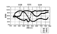
ここで、図4は、横軸をカラーフィルタ522への入射光の波長とし、縦軸を透過率(入射光量に対する出射光量の割合)として、カラーフィルタ522R、522Gおよび522Bの各々の透過率特性を表すグラフである。同図に示すように、カラーフィルタ522Rは赤色に対応する波長600nm以上の光に対して高い透過率を示し、カラーフィルタ522Gは緑色に対応する波長500ないし600nmの光に対して高い透過率を示し、カラーフィルタ522Gは青色に対応する波長400ないし500nmの光に対して高い透過率を示すようになっている。
【0043】
次に、再び図3を参照して、半透過反射層521に形成された開口部521aの態様について説明する。
まず、各開口部521aは、半透過反射層521のうち各サブ画素551の中央部近傍に対応して設けられている。照明装置5からの照明光は、この開口部521aを透過して液晶表示パネル500の観察側に出射し、これにより透過型表示が実現される。以下では、サブ画素551が占める領域のうち、開口部521aに対応する領域、すなわち照明装置5からの照明光が透過する領域を「透光領域(光透過領域)」と表記する。
【0044】
さらに、半透過反射層521に形成された各開口部521aは、ひとつの画素615を構成する3つのサブ画素551R、551Gおよび551Bの各々において上記透光領域の面積が相互に異なるように、その面積が選定されている。より具体的には、サブ画素551R、551Gおよび551Bの各々に対応する開口部521aの面積が、照明装置5から出射する照明光の分光特性に応じた面積となっている。
【0045】
本実施形態においては、図2に示したように、照明装置5から出射される照明光のうち、青色光から緑色光にかけての波長における輝度が高く、赤色光に対応する波長における輝度は比較的低くなっている。このため、最も輝度が高い波長に対応する緑色のカラーフィルタ522Gが形成されたサブ画素551Gについては、これに対応する開口部521aの面積が他色に対応するサブ画素551Rおよび551Bと比較して小さくなっている。これに対し、照明光のうち最も輝度が低い波長に対応する赤色のカラーフィルタ522Rが形成されたサブ画素551Rについては、これに対応する開口部521aの面積が他色のサブ画素551Gおよび551Bと比較して大きくなっている。図3においては、サブ画素551R、551Gおよび551Bの各々に対応する開口部521aの面積比を、「サブ画素551R:551G:551B=4:1:2」とした場合が図示されている。
【0046】
ここで、図5は、以上説明した構成により透過型表示を行った場合に、液晶表示パネル500から観察側に出射する観察光の分光特性を表すグラフである。一方、図6には、図5との対比例として、透光領域をすべてのサブ画素551にわたって同一面積とした構成(以下、「従来の構成」という。)の下で透過型表示を行った場合の観察光の分光特性が示されている。なお、いずれの図においても、図2に示した分光特性を有する照明光を用いて透過型表示を行った場合の観察光の分光特性が示されている。また、図5および図6のいずれにおいても、横軸には波長が示されており、縦軸には各観察光の輝度が、所定の輝度(図5および図6の双方において同一の輝度)を基準値「1.00」とした場合の相対値として示されている。
【0047】
図6に示すように、従来の構成を採った場合、観察者によって視認される観察光は波長470nm近傍において極めて高い輝度の光となる。したがって、観察者に認識される画像は青緑がかった画像となってしまう。これに対し、サブ画素551R、551Gおよび551Bにおける透光領域の割合を4:1:2とした本実施形態に係る構成を採った場合、図5に示すように、観察光の波長470nm近傍における輝度が図6に示した場合と比較して低くなっている。したがって、青色ないし緑色に対応する波長における輝度が他の波長における輝度よりも強い照明光を用いて透過型表示を行った場合であっても、観察者に視認される画像が青緑がかってしまうという事態を回避することができるのである。
【0048】
このように、本実施形態に係る構成によれば、照明光のうち輝度が比較的低い波長の光については半透過反射層521を十分に透過させる一方、輝度が比較的高い波長の光については半透過反射層521の透過を制限することにより、照明光における分光特性のばらつきが観察光に与え得る影響を抑えることができる。すなわち、照明光における分光特性の不均一性を補償して良好な色再現性を実現することができるのである。
【0049】
<B:第2実施形態:液晶表示装置>
次に、本発明をアクティブマトリクス方式の半透過反射型液晶表示装置に適用した第2実施形態について説明する。なお、以下では、スイッチング素子として二端子型スイッチング素子であるTFD(Thin Film Diode)を用いた場合を例示する。また、以下に示す図面中の各要素のうち、前掲図1に示した各要素と共通する要素については、図1中と同一の符号を付してその説明を省略する。
【0050】
まず、図7は、本実施形態に係る液晶表示装置の構成を模式的に例示する断面図であり、図8は、同液晶表示装置を構成する液晶表示パネルの要部構成を示す斜視図である。図8におけるA−A’からみた断面図が図7に相当する。これらの図に示すように、第1基板3の内側表面には、マトリクス状に配列する複数の画素電極513と、各画素電極513の間隙部分において所定の方向(図7における紙面垂直方向)に延在する複数の走査線514とが形成されている。各画素電極513は、例えばITO等の透明導電材料により形成される。さらに、各画素電極513と、当該画素電極513に隣接する走査線514とは、TFD515を介して接続されている。各TFD515は、非線形な電流−電圧特性を有する二端子型スイッチング素子である。
【0051】
一方、第2基板2の内側表面には、上記第1実施形態に係る液晶表示装置と同様に、複数の開口部521aを有する半透過反射層521と、カラーフィルタ522および遮光層523と、これらが形成された第2基板2の表面を覆うオーバーコート層524とが形成されている。さらに、オーバーコート層524の表面には、上記走査線514と交差する方向に延在する複数のデータ線527が形成されている。図7および8に例示するように、各データ線527は透明導電材料により形成された帯状の電極である。ここで、図9には、各画素電極513(一点鎖線で示されている)と各データ線527との位置関係が示されている。同図に示すように、各データ線527は、第1基板3上に列をなす複数の画素電極513と対向するようになっている。かかる構成の下、第1基板3上の画素電極513と第2基板2上のデータ線527との間に電圧が印加されることにより、両電極によって挟まれた液晶4の配向状態が変化する。すなわち、本実施形態においては、各画素電極513と各データ線527とが対向する領域がサブ画素551(より具体的には、カラーフィルタ522R、522Gおよび522Bの各々に対応するサブ画素551R、551Gおよび551B)に相当することとなる。
【0052】
上記第1実施形態と同様、本実施形態においても、図9に示すように、半透過反射層521のうち各サブ画素551の中央部近傍に対応する位置には開口部521aが形成されている。そして、各開口部521aの面積は、各サブ画素551R、551Gおよび551Bの各々に占める透光領域の割合が、照明装置5からの照明光の分光特性に応じた割合となるように決定されている。ここで、本実施形態においても、前掲図2に示した分光特性を有する照明光を用いて透過型表示を行う場合を想定している。したがって、照明光のうち最も輝度が高い波長に対応する緑色のカラーフィルタ522Gが形成されたサブ画素551Gにおいては、これに対応する開口部521aの面積が、他色に対応するサブ画素551Rまたは551Bに対応する開口部521aの面積と比較して小さくなっている。すなわち、サブ画素551Gに占める透光領域の割合は、他色のサブ画素551Rまたは551Bに占める透光領域の割合よりも小さくなっている。これに対し、照明光のうち最も輝度が低い波長に対応するサブ画素551Rについては、開口部521aの面積が大きく、当該サブ画素551Rに占める透光領域の割合が、他色のサブ画素551Gおよび551Bと比較して大きくなっているのである。図9に示した例では、サブ画素551R、551Gおよび551Bの各々に対応する開口部521aの面積比を「4:1:2」とした場合が図示されている。
かかる構成によっても、上記第1実施形態と同様の効果が得られる。
【0053】
<C:第3実施形態:液晶表示装置>
上記第1および第2実施形態においては、半透過反射層521のうち各サブ画素551に対応する領域の中央部近傍に開口部521aを設け、透光領域が各サブ画素551の中央部に位置する構成を例示した。これに対し、本実施形態においては、透光領域が各サブ画素551の縁辺に沿った領域となっている。
【0054】
図10は、本実施形態に係る液晶表示装置の構成を示す断面図である。なお、図10に示す要素のうち前掲図1に示した要素と共通するものについては、同一の符号が付されている。同図に示すように、本実施形態に係る液晶パネル500においては、カラーフィルタ522(522R、522Gおよび522B)、遮光層523およびオーバーコート層524が第1基板3上に形成されている点、および透明電極511および配向膜15がオーバーコート層の面上に形成されている点で、上記各実施形態に示した液晶パネル500とは異なっている。さらに、本実施形態におけるカラーフィルタ522の透過率特性は、前掲図4に示した上記各実施形態におけるカラーフィルタ522の透過率特性とは異なっている。
【0055】
ここで、図11は、本実施形態におけるカラーフィルタ522R、522Gおよび522Bの各々の透過率特性を表すグラフである。この図を前掲図4と比較すれば判るように、本実施形態に係る各カラーフィルタ522の色純度、特に緑色に対応するカラーフィルタ522Gの色純度は、上記実施形態に係るカラーフィルタ522の色純度よりも高くなっている。より具体的には、以下の通りである。
【0056】
ここで、380nm〜780nmの波長範囲における各カラーフィルタ522の最大透過率をTmaxとし、同波長範囲における最小透過率をTminとして得られる数値Tmax/Tminを、色純度を評価するためのパラメータ(つまり、数値Tmax/Tminが大きいほど色純度が高い)として考える。このとき、前掲図4に示した緑色のカラーフィルタ522Gの数値Tmax/Tminは「1.8」であるのに対し、本実施形態に係るカラーフィルタ522Gの数値Tmax/Tminは「8」であり、本実施形態に係るカラーフィルタ522Gの色純度が、上記実施形態に係るカラーフィルタ522Gの色純度よりも顕著に高いことが判る。
【0057】
また、本実施形態においては、半透過反射層528の態様が上記第1および第2実施形態とは異なっている。すなわち、上記実施形態においては、各サブ画素551の中央部に位置する領域が透光領域となるように、半透過反射層521の形状(より詳細には半透過反射層521における開口部521aの形状)が選定された構成を例示した。これに対し、本実施形態においては、略矩形状の各サブ画素551を画定する4辺のうち対向する2辺(Y方向に伸びる2辺)に沿った領域が透光領域となるように、半透過反射層528の形状が選定されている。以下、図12を参照して、半透過反射層528の具体的な形状について説明する。
【0058】
図12に示すように、本実施形態における半透過反射層528は、第2基板2上においてY方向に延在する複数の部分を有する。一方、透明電極525は、上記実施形態に示したものと同様の形状であるが、当該半透過反射層528を覆うように形成される点で異なっている。このように、本実施形態における半透過反射層528は、各透明電極525に対応するようにストライプ状に形成されているのである。換言すると、半透過反射層528には、当該各透明電極525の間隙部分に沿った形状の透光部(照明装置からの照明光を透過させる部分)528aが形成されているということができる。半透過反射層528に対してかかる形状の透光部528aが形成されている結果、図12に示すように、略矩形状の各サブ画素551の周縁を画定する4辺のうち、Y方向に伸びる対辺に沿った領域が透光領域として機能することとなる。
【0059】
そして、本実施形態においても、上記第1および第2実施形態と同様に、少なくとも一のサブ画素551に占める透光領域の面積と、他のサブ画素551に占める透光領域の面積とが異なるように、半透過反射層528の形状が選定されている。
より具体的には、図12に示すように、サブ画素551Rの列に対応する反射層の幅Wrと、サブ画素551Bの列に対応する反射層の幅Wbとがほぼ等しく、サブ画素551Gの列に対応する反射層の幅Wbは、幅Wrおよび幅Wbよりも広くなっている。したがって、サブ画素551Rに占める透光領域の面積Srと、サブ画素551Bに占める透光領域の面積Sbとがほぼ等しく、サブ画素551Gに占める透光領域の面積Sgは、面積Srまたは面積Sbよりも小さい。ここでは、面積Srと面積Sgと面積Sbとの比が、「Sr:Sg:Sb=1.5:1:1.5」とした場合を想定している。
【0060】
ところで、図4に示したように、上記実施形態に示した緑色のカラーフィルタ522Gの透過率は、他色のカラーフィルタ522Rまたは522Bの透過率と比較して著しく高い。したがって、図4に示した透過率特性を有するカラーフィルタ522を用いて理想的な白表示を行なう(つまり色再現性を補償する)ためには、緑色のサブ画素551Gに占める透光領域の面積を、他色のサブ画素551Rまたは551Bに占める透光領域の面積よりも顕著に小さくする必要がある。これに対し、図11に透過率特性を示したカラーフィルタ522Gは、図4に示したカラーフィルタ522Gよりも透過率が低く抑えられているため、緑色のサブ画素551Gに占める透光領域の面積と、他色のサブ画素551Rまたは551Bに占める透光領域の面積との差異を、図4に示したカラーフィルタ522を用いた場合ほどに大きく確保する必要がない。すなわち、図11に透過率特性を示したカラーフィルタ522Gを用いることによって、緑色のサブ画素551Gに占める透光領域の面積をそれほど小さくする必要がなくなるのである。
【0061】
ここで、図13は、本実施形態に係る液晶表示装置によって表示される色の色座表を表すCIE色度図である。図13においては、従来の構成の液晶表示装置によって表示される色の色座標が、本実施形態の対比例として示されている。なお、「従来の構成」の液晶表示装置とは、図13に透過率特性を示したカラーフィルタを用い、かつ全てのサブ画素について透光領域の面積を同一とした構成の液晶表示装置である。
【0062】
CIE色度図において、理想的な白表示を行なった場合の色座標は、概ね(x,y)=(0.310,0.316)であり、図13にはこの点が「×」により示されている。同図からも明らかなように、本実施形態に係る液晶表示装置によって白表示を行なった場合の色座標は、従来の構成の液晶表示装置によって白表示を行なった場合の色座標と比較して、理想的な白表示の色座標に近づいている。すなわち、本実施形態に係る液晶表示装置によれば、良好な色再現性が実現されているということができる。
【0063】
本実施形態によっても、上記各実施形態と同様に、照明光における分光特性のばらつきが観察光に与え得る影響を抑えて、良好な色再現性が実現されるという効果が得られる。
【0064】
本実施形態および上記各実施形態に示したように、本発明においては、画素を構成するいずれかのサブ画素に占める透光領域の割合と、当該画素を構成する他のサブ画素に占める透光領域の割合とが異なっていれば、各サブ画素における透光領域の態様、すなわち半透過反射層521における透光部(開口部521aまたは透光部528a)の態様は、いかなるものであってもよい。また、本発明における「透光部」は、「半透過反射層のうち、照明装置からの照明光を透過させる部分」を意味し、半透過反射層に形成された開口部(すなわち孔)に限定されるものではない。
【0065】
<D:変形例>
以上この発明の一実施形態について説明したが、上記実施形態はあくまでも例示であり、上記実施形態に対しては、本発明の趣旨から逸脱しない範囲で様々な変形を加えることができる。変形例としては、例えば以下のようなものが考えられる。
【0066】
<D−1:変形例1>
上記第1および第2実施形態においては、照明装置5からの照明光の分光特性に応じて、各サブ画素551に対応する開口部521aの面積を異ならせるようにしたが、以下のようにしてもよい。すなわち、図14に示すように、半透過反射層521に設けられる各開口部521aの面積を略同一とする一方、各サブ画素551に対応して設けられる開口部521aの個数を、照明光の分光特性に応じた個数とするのである。
【0067】
例えば、上記各実施形態においては、前掲図2に示した照明光の分光特性に応じて、サブ画素551R、551Gおよび551Bに対応する開口部521aの面積比を「4:1:2」としたが、本変形例においては、図14に示すように、サブ画素551R、551Gおよび551Bに対応する開口部521aの個数の比を「4:1:2」とするのである。かかる構成とした場合にも、上記各実施形態と同様の効果を得ることができる。さらに、上記各実施形態に示したように、各サブ画素551の一部分のみに対応して開口部521aを形成した場合、各サブ画素615において各開口部521aの位置が偏ってしまう結果、観察者によって視認される画像にざらつき感が生じることも考えられるが、本変形例に示した構成によれば、各サブ画素551において開口部521aを散在させることができるから、このような不具合を回避することができるという利点がある。
【0068】
<D−2:変形例2>
上記各実施形態においては、同一色に対応するサブ画素551ごとに、当該サブ画素551に占める透光領域の割合を異ならせるようにした。照明装置5からの照明光の分光特性が、液晶表示パネル500の基板面の全面において同一であれば、かかる構成を採用した場合にも、照明光の分光特性の不均一性を十分に補償することが可能である。しかしながら、照明装置5からの照明光の分光特性が、基板面内の各箇所において異なる場合もあり得る。例えば、基板面内のある箇所には図2に示した分光特性を有する照明光が照射されるが、他の箇所には図2に示したのと異なる分光特性を有する照明光が照射されるといった具合である。かかる場合には、基板面内における各サブ画素551の位置に応じて透光領域の割合を異ならせる(つまり、開口部521aの面積を異ならせる)ようにしてもよい。例えば、図2に示した分光特性を有する照明光が照射される箇所に位置する画素615においては、各サブ画素551R、551Gおよび551Bにおける透光領域の面積比を「4:1:2」とする一方、この照明光と比較して青色光から緑色光にかけての輝度が若干低い照明光が照射される箇所の画素615においては、各サブ画素551R、551Gおよび551Bにおける透光領域の面積比を「3:1:2」とする、といった具合である。このように、同一色に対応するサブ画素551における透光領域の割合は、必ずしもすべてのサブ画素551にわたって同一である必要はないのである。本変形例によれば、上記各実施形態に示した効果に加え、照明光の分光特性が基板面内において不均一である場合にもこれを補償することができるから、より確実に色再現性を向上させることができるという効果が得られる。
【0069】
<D−3:変形例3>
上記各実施形態においては、照明装置からの照明光が図2に示す分光特性を示す場合を例示したが、照明光の分光特性がこれに限られるものでないことは言うまでもない。すなわち、図2とは異なる分光特性を示す照明光を透過型表示に際して用いる場合にも、例えば、当該照明光のうち輝度が高い波長に対応する色のサブ画素における透光領域の面積を、輝度が低い波長に対応する色のサブ画素における透光領域の面積よりも小さくするといった具合に、照明光の分光特性に応じた面積とすれば、照明光の分光特性のばらつきを補償して良好な色再現性を実現することができるという効果を得ることができる。
【0070】
さらには、各サブ画素における透光領域の面積は、必ずしも照明光の分光特性に応じたものでなくてもよい。例えば、照明光の分光特性とは無関係に、緑色に対応するサブ画素551Gまたは青色に対応するサブ画素551Bにおける透光領域の面積(つまり、これらのサブ画素551に対応する開口部521aの面積)を、赤色に対応するサブ画素551Rにおける透光領域の面積よりも広くすれば、表示を意図的に青緑がかったものにすることができる。つまり、本発明においては、一のサブ画素551における透光領域の面積が、他のサブ画素551における透光領域の面積と異なるように、半透過反射層521における開口部521aの面積が選定されていればよいのである。
【0071】
<D−4:変形例4>
上記第3実施形態においては、各サブ画素を画定する4辺のうち対向する二辺に沿った領域が透光領域となる場合を例示したが、これらの4辺のうち1辺、3辺または全ての辺(4辺)に沿った領域が透光領域となるように、半透過反射層528の形状を選定してもよい。すなわち、透光領域をサブ画素の縁辺に沿った領域とする場合には、各サブ画素を画定する複数の辺のうち少なくとも一辺に沿った領域を透光領域とすればよい。また、上記第3実施形態においては、複数のサブ画素551にわたって連なった形状の半透過反射層528を例示したが、半透過反射層528を各サブ画素551ごとに離間した形状としてもよい。
【0072】
<D−5:変形例5>
上記各実施形態においては、同一色のカラーフィルタ522が一列をなすストライプ配列を採用した場合を例示したが、カラーフィルタ522の配列の態様としては、この他にもモザイク配列やデルタ配列を採用することもできる。
【0073】
また、上記各実施形態においては、第2基板2の内側表面に半透過反射層521を形成する場合を例示したが、第2基板2の外側表面に反射層を形成することも考えられる。要は、半透過反射層521が液晶4に対して観察側とは反対側に位置する構成であればよい。
【0074】
<D−6:変形例6>
上記第2実施形態においては、スイッチング素子としてTFD515を採用したアクティブマトリクス方式の液晶表示装置を例示したが、本発明の適用範囲はこれに限られるものではなく、TFT(Thin Film Transistor)に代表される三端子型スイッチング素子を採用した液晶表示装置にも適用できる。なお、TFTを用いた場合、一方の基板の全面にわたって対向電極が形成され、他方の基板上には複数の走査線と複数のデータ線とが相互に交差する方向に延在して形成されるとともに、これらの双方にTFTを介して接続された画素電極がマトリクス状に配列して形成されることとなる。この場合、各画素電極と対向電極とが対向する領域がサブ画素として機能することとなる。
【0075】
<D−7:変形例7>
上記各実施形態においては、半透過反射層521と透明電極525(第2実施形態においてはデータ線527)とが別個に形成される場合を例示したが、液晶4に電圧を印加するための電極を光反射性を有する導電材料により形成し、この電極が半透過反射層521としての機能を兼ね備えるようにしてもよい。すなわち、図1に示した半透過反射層521を設けることなく、透明電極525に代えて、これと同様の形状の反射電極を設けるのである。この場合、反射電極のうちの各サブ画素に対応する領域(つまり、第1基板3上の透明電極511と対向する領域)の一部に、上記各実施形態および各変形例に例示した態様の開口部が設けられることとなる。
【0076】
<E:第4実施形態:液晶表示装置>
図15は、本発明の液晶表示装置の一例を示した図であり、カラーフィルタが下基板の内面側に設けられているパッシブマトリクス方式の半透過反射型カラー液晶表示装置の一例を示した部分断面図である。また、図16は、図15に示した液晶表示装置における半透過反射層とカラーフィルタと遮光膜のみを示した図であり、図16(A)は、半透過反射層とカラーフィルタとの重なり合いを説明するための平面図であり、図16(B)は、図16(A)に示すA−A’線に沿う断面図である。
なお、以下の図面においては、図面を見やすくするため、各構成要素の膜厚や寸法の比率などは適宜異ならせてある。
【0077】
図15に示した液晶表示装置は、液晶パネル(液晶表示パネル)1と、この液晶パネル1の後面側(下基板2の外面側)に配設されたバックライト(照明装置)5とを備えて概略構成されている。
また、液晶パネル1は、対向配置された下基板2と上基板3とに挟まれた空間に、STN(Super Twisted Nematic)液晶などからなる液晶層4が挟持されて概略構成されている。
【0078】
下基板2は、ガラスや樹脂などからなるものであり、下基板2の内面側には、半透過反射層6が設けられ、半透過反射層6の上側には、カラーフィルタ10が積層され、カラーフィルタ10を構成する各色素層11R、11G、11B間には、黒色樹脂材料などからなる遮光膜41が設けられている。また、カラーフィルタ10の上には、カラーフィルタ10によって形成された凹凸を平坦化するための透明な平坦化膜12が積層されている。さらに、平坦化膜12上には、インジウム錫酸化物(Indium Tin Oxide, 以下、「ITO」と略記する。)等の透明導電膜からなるストライプ状の透明電極(セグメント電極)8が紙面垂直方向に延在し、透明電極8の上側には、透明電極8を覆うようにポリイミド等からなる配向膜9が設けられている。
また、下基板2の外面側には、1/4波長板18と、下偏光板14と、反射偏光子19とが設けられている。
【0079】
一方、上基板3は、ガラスや樹脂などからなるものであり、上基板3の内面側には、ITO等の透明導電膜からなるストライプ状の透明電極(コモン電極)7が、下基板2に設けられている透明電極8と直交する方向(図示横方向)に延在し、透明電極7の下側には、透明電極7を覆うようにポリイミド等からなる配向膜15が設けられている。
また、上基板3の外面側には、前方散乱板16と、位相差板17と、上偏光板13とが、この順に上基板3上に積層されて設けられている。
【0080】
また、バックライト5の下面側(液晶パネル1と反対側)には、反射板51が設けられている。
【0081】
次に、図15に示した液晶表示装置における半透過反射層6とカラーフィルタ10との平面的な重なり合いを説明する。
半透過反射層6は、アルミニウム等の反射率の高い金属膜からなるものであり、図16に示すように、金属膜を窓状に開口することにより形成され、バックライト5から出射された光や上基板3側から入射する光を透過する光透過領域6aと、上基板3側から入射する光を反射する光反射領域6bとを各画素毎に有している。
【0082】
一方、カラーフィルタ10は、表示領域を構成する各画素に対応して設けられ、上述した上基板3に設けられている透明電極7と直交するように、赤色層11Rと緑色層11Gと青色層11Bとが紙面垂直方向に延在し、赤色層11R、緑色層11G、青色層11Bの順番に繰り返し配列された色素層11を有するものである。
【0083】
各色素層11R、11G、11Bは、図16に示すように、半透過反射層6の光透過領域6aと平面的に重なる領域の全体と、各色素層11R、11G、11Bを窓状に開口することにより、半透過反射層6の光反射領域6bと平面的に重なる領域の一部を除いた領域とに設けられている。このことにより、カラーフィルタ10には、各色素層11R、11G、11Bが設けられている色素層形成領域と、光反射領域6bと平面的に重なる領域の一部であり、各色素層11R、11G、11Bが設けられていない領域である色素層非形成領域11D、11E、11Fとが存在している。また、この液晶表示装置においては、色素層形成領域の面積、すなわち各色素層11R、11G、11Bの面積は、赤色層11R、青色層11B、緑色層11Gの順で小さくなるように設けられている。
【0084】
このような液晶表示装置では、図15に示すように、反射モード時に上基板3側から液晶表示装置に入射した外光30aは、カラーフィルタ10を透過し、半透過反射層6の光反射領域6bによって反射され、再びカラーフィルタ10を透過して、上基板3側から外部に向かって出射される。反射モード時に上基板3側から液晶表示装置に入射した外光30bは、カラーフィルタ10を通過せずに光反射領域6bによって反射され、上基板3側から外部に向かって出射される。反射モード時に上基板3側から液晶表示装置に入射した外光30cは、光透過領域6aを通過するため、反射光とはならない。
つまり反射光には、各色素層11R、11G、11Bを透過する光30aと色素層非形成領域11D、11E、11Fを透過する光30bとがあり、各色素層11R、11G、11Bを透過した光30aのみが着色され、色素層非形成領域11D、11E、11Fを透過した光30bは着色されない。
【0085】
したがって、反射モード時に上基板3側から外部に向かって出射される光は、各色素層11R、11G、11Bを透過した着色された光30aと色素層非形成領域11D、11E、11Fを透過した着色されない光30bとを合わせた光となる。
【0086】
また、透過モード時にバックライト5から液晶表示装置に入射した光50aは、光透過領域6aを透過し、カラーフィルタ10の色素層11を透過して着色される。また、透過モード時にバックライト5から液晶表示装置に入射した光50bは、半透過反射層6により遮光される。
したがって、透過モード時に上基板3側から外部に向かって出射される光は、カラーフィルタ10の色素層11を1回透過した着色された光50aとなる。
【0087】
このような液晶表示装置は、光反射領域6bと平面的に重なる領域の一部に色素層非形成領域11D、11E、11Fがあるので、上述したように、反射モード時に得られる光は、色素層非形成領域11D、11E、11Fを透過した着色されない光30bと色素層11を透過した着色された光30aとを合わせた光となる。一方、透過モード時に得られる光は、色素層11を透過する着色された光50aのみとなる。
【0088】
このことにより、反射モード時にカラーフィルタ10を2回透過することによって得られる光と、透過モード時にカラーフィルタ10を1回透過することによって得られる光との色の濃淡差を少なくすることができる。
その結果、反射モード時にも透過モード時にも同様に、明るく、視認性の高い表示ができるカラーの半透過反射型液晶表示装置を実現することが可能となる。しかも、図15に示した液晶表示装置においては、前記色素層11は、赤色層11Rと緑色層11Gと青色層11Bとからなり、各色素層11R、11G、11Bの面積は、赤色層11R、青色層11B、緑色層11Gの順で小さくなるように設けられ、カラーフィルタ10の色特性を、各色素層11R、11G、11Bの面積を変化させて調整することにより、より一層、色再現性を向上させることができ、より優れた表示品質を有する液晶表示装置を実現することができる。
【0089】
また、図15に示した液晶表示装置においては、各色素層11R、11G、11Bが設けられている領域と色素層非形成領域11D、11E、11Fとの段差を平坦化する透明膜12が設けられているので、各色素層11R、11G、11Bが設けられている領域と色素層非形成領域11D、11E、11Fとの段差に起因する悪影響が発生しないものとすることができ、液晶表示装置の信頼性を向上させることができる。
【0090】
また、厚みを薄くした金属膜にて作成した半透過反射層は、光の反射、透過以外に、光の吸収を持つのに対し、図15に示した液晶表示装置は、半透過反射層6が窓状に開口されることにより、光透過領域6aが形成されたものであるので、光の吸収を持たず、反射率、透過率を高くすることが出来る。
【0091】
<F:第5実施形態:液晶表示装置>
第5実施形態において、液晶表示装置の全体構成は、図15に示した第4実施の形態と同様であるため、詳細な説明は省略する。
また、第5実施形態の液晶表示装置が、第4実施形態の液晶表示装置と異なるところは、半透過反射層およびカラーフィルタの形状のみであるので、半透過反射層およびカラーフィルタについて、図17を用いて詳しく説明する。
図17は、第5実施形態の液晶表示装置における半透過反射層とカラーフィルタと下基板の透明電極のみを示した図であり、図17(A)は、半透過反射層とカラーフィルタとの重なり合いを説明するための平面図であり、図17(B)は、図17(A)に示すC−C’線に沿う断面図である。
なお、図17において、第4実施形態と共通の構成要素には同一の符号を付している。
【0092】
半透過反射層61は、下基板2に設けられている透明電極8と同様に、上基板3に設けられている透明電極7と直交するように紙面垂直方向にストライプ状に延在して設けられ、下基板2に設けられている透明電極8と同様のピッチで形成されている。そして、図17(B)に示すように、半透過反射層61を構成する金属膜のパターンの幅よりも、下基板2に設けられている透明電極8のパターンの幅の方が大きく形成されることにより、半透過反射層61を構成する金属膜と透明電極8とが平面的に重ならない帯状の領域が光透過領域61aとされ、金属膜が設けられている領域の全体が光反射領域61bとされている。
【0093】
一方、カラーフィルタ101は、第4実施形態と同様に、表示領域を構成する各画素に対応して設けられ、上基板3に設けられている透明電極7と直交するように赤色層111Rと緑色層111Gと青色層111Bとが紙面垂直方向に延在し、赤色層111R、緑色層111G、青色層111Bの順番に繰り返し配列された色素層111を有するものである。
【0094】
各色素層111R、111G、111Bは、図17に示すように、半透過反射層61の光透過領域61aと平面的に重なる領域の全体と、各色素層111R、111G、111Bをストライプ状に開口することにより、半透過反射層61の光反射領域61bと平面的に重なる領域の一部を除いた領域とに設けられている。
このことにより、カラーフィルタ101には、各色素層111R、111G、111Bが設けられている色素層形成領域と、光反射領域61bと平面的に重なる領域の一部であり、各色素層111R、111G、111Bが設けられていない領域である色素層非形成領域111D、111E、111Fとが存在している。また、この液晶表示装置においては、第4実施形態と同様に、色素形成領域の面積、すなわち各色素層111R、111G、111Bの面積は、赤色層111R、青色層111B、緑色層111Gの順で小さくなるように設けられている。
【0095】
このような液晶表示装置も、第4実施形態と同様に、半透過反射層61の光反射領域61bと平面的に重なる領域の一部に色素層非形成領域111D、111E、111Fが形成されているので、反射モード時に液晶表示装置に入射した外光のうちの一部は、色素層非形成領域111D、111E、111Fを透過することになり、反射モード時にカラーフィルタ101を2回透過することによって得られる光は、色素層非形成領域111D、111E、111Fを透過する着色されない光と色素層111を透過する着色された光とを合わせた光となる。一方、透過モード時にバックライト5から入射して光透過領域61aを透過した光は、全て色素層111を透過することになり、透過モード時にカラーフィルタ101を1回透過することによって得られる光は、全て着色された光となる。このことにより、反射モード時にカラーフィルタを2回透過することによって得られる光と、透過モード時にカラーフィルタを1回透過することによって得られる光との色の濃淡差を少なくすることができる。
【0096】
その結果、反射モード時にも透過モード時にも同様に、発色がよく、視認性の高い表示ができるカラーの半透過反射型液晶表示装置を実現することが可能となる。
しかも、本実施形態の液晶表示装置においても、前記色素層111は、赤色層111Rと緑色層111Gと青色層111Bとからなり、各色素層111R、111G、111Bの面積は、赤色層111R、青色層111B、緑色層111Gの順で小さくなるように設けられ、カラーフィルタ101の色特性を、各色素層111R、111G、111Bの面積を変化させて調整することにより、より一層、色再現性を向上させることができ、より優れた表示品質を有する液晶表示装置を実現することができる。
【0097】
また、このような液晶表示装置では、半透過反射層61が、半透過反射層61を構成する金属膜のパターンの幅よりも、下基板2に設けられている透明電極8のパターンの幅の方が大きく形成されることにより、帯状の光透過領域61aと光反射領域61bとが形成されたものであるので、窓状に開口部を設けた半透過反射層と比較して、開口部の長さ方向のばらつきが無くなるため、製造上安定である。
【0098】
<G:第6実施形態:液晶表示装置>
図18は、本発明の液晶表示装置の他の例を示した図であり、カラーフィルタが上基板の内面側に設けられているパッシブマトリクス方式の半透過反射型カラー液晶表示装置の一例を示した部分断面図である。また、図19は、図18に示した液晶表示装置における半透過反射層とカラーフィルタのみを示した図であり、図19(A)は、半透過反射層とカラーフィルタとの重なり合いを説明するための平面図であり、図19(B)は、図19(A)に示すB−B’線に沿う断面図である。
なお、図18および図19において、第4実施形態と共通の構成要素には同一の符号を付し、詳細な説明は省略する。
【0099】
図18に示した液晶表示装置は、液晶パネル100と、この液晶パネル100の後面側(下基板2の外面側)に配設されたバックライト(照明装置)5とを備えて概略構成されている。
また、液晶パネル100は、第4実施形態と同様に、対向配置された下基板2と上基板3とに挟まれた空間に、液晶層4が挟持されて概略構成されている。
【0100】
下基板2の内面側には、半透過反射層6と、絶縁膜23とがこの順に積層され、絶縁膜23の上側には、ITO等の透明導電膜からなるストライプ状の透明電極8(ここではコモン電極)が図示横方向に延在し、透明電極8の上側には、透明電極8を覆うように配向膜9が設けられている。
また、下基板2の外面側には、第4実施形態と同様に、1/4波長板18と、下偏光板14と、反射偏光子19とが設けられている。
【0101】
一方、上基板3の内面側には、カラーフィルタ20が積層され、カラーフィルタ20を構成する各色素層21R、21G、21B間には、黒色樹脂材料などからなる遮光膜42が設けられている。また、カラーフィルタ20の下側には、カラーフィルタ20によって形成された凹凸を平坦化するための透明な平坦化膜22が積層されている。さらに、平坦化膜22下側には、ITO等の透明導電膜からなるストライプ状の透明電極7(ここではセグメント電極)が、下基板2に設けられている透明電極8と直交する方向(紙面垂直方向)に延在し、透明電極7の下側には、透明電極7を覆うように配向膜15が設けられている。
また、上基板3の外面側には、第4実施形態と同様に、前方散乱板16と、位相差板17と、上偏光板13とが、この順に上基板3上に積層されて設けられている。
【0102】
また、バックライト5の下面側(液晶パネル1と反対側)には、第4実施形態と同様に、反射板51が設けられている。
【0103】
次に、図18に示した液晶表示装置における半透過反射層とカラーフィルタとの平面的な重なり合いを説明する。図18に示した液晶表示装置においては、図15に示した第4実施形態の液晶表示装置とカラーフィルタの配置されている位置が異なっているが、半透過反射層とカラーフィルタとの平面的な重なり合いは、第4実施形態と同様となっている。
半透過反射層6は、第4実施形態と同様であり、図19に示すように、金属膜を窓状に開口することにより形成され、光透過領域6aと、光反射領域6bとを各画素毎に有している。
【0104】
一方、カラーフィルタ20は、下基板2に設けられている透明電極8と直交するように赤色層21Rと緑色層21Gと青色層21Bとが紙面垂直方向に延在し、赤色層21R、緑色層21G、青色層21Bの順番に繰り返し配列された色素層21を有するものである。
【0105】
各色素層21R、21G、21Bは、図19に示すように、半透過反射層6の光透過領域6aと平面的に重なる領域の全体と、各色素層21R、21G、21Bを窓状に開口することにより、半透過反射層6の光反射領域6bと平面的に重なる領域の一部を除いた領域とに設けられている。このことにより、カラーフィルタ20には、色素層21が設けられている色素層形成領域と、光反射領域6bと平面的に重なる領域の一部であり、各色素層21R、21G、21Bが設けられていない領域である色素層非形成領域21D、21E、21Fとが存在している。また、この液晶表示装置においても、第4実施形態と同様に、色素形成領域の面積、すなわち各色素層21R、21G、21Bの面積は、赤色層21R、青色層21B、緑色層21Gの順で小さくなるように設けられている。
【0106】
このような液晶表示装置においても、図18に示すように、反射モード時に上基板3側から外部に向かって出射される光は、各色素層21R、21G、21Bを透過する光30aと色素層非形成領域21D、21E、21Fを透過する光30bとがあり、各色素層21R、21G、21Bを透過した光30aのみが着色され、色素層非形成領域21D、21E、21Fを透過した光30bは着色されない。したがって、このような液晶表示装置においても、第4実施形態と同様に、反射モード時に上基板3側から外部に向かって出射される光は、着色されない光30bと着色された光30bとを合わせた光となる。
【0107】
一方、透過モード時に上基板3側から外部に向かって出射される光も、第4実施形態と同様に、カラーフィルタ20の色素層21を1回透過した着色された光50aとなる。
【0108】
このことにより、本実施形態の液晶表示装置においても、反射モード時にカラーフィルタ20を2回透過することによって得られる光と、透過モード時にカラーフィルタ20を1回透過することによって得られる光との色の濃淡差を少なくすることができる。
その結果、反射モード時にも透過モード時にも同様に、発色がよく、視認性の高い表示ができるカラーの半透過反射型液晶表示装置を実現することが可能となる。
【0109】
しかも、図19に示した液晶表示装置においても、前記色素層21は、赤色層21Rと緑色層21Gと青色層21Bとからなり、各色素層21R、21G、21Bの面積は、赤色層21R、青色層21B、緑色層21Gの順で小さくなるように設けられ、カラーフィルタ20の色特性を、各色素層21R、21G、21Bの面積を変化させて調整することにより、より一層、色再現性を向上させることができ、より優れた表示品質を有する液晶表示装置を実現することができる。
【0110】
<H:第7実施形態:液晶表示装置>
図20は、本発明の液晶表示装置の他の例を示した図であり、半透過反射層上に透明電極が直接設けられているパッシブマトリクス方式の半透過反射型カラー液晶表示装置の一例を示した部分断面図である。また、図21は、図20に示した液晶表示装置における半透過反射層とカラーフィルタと下基板の透明電極のみを示した図であり、図21(A)は、半透過反射層とカラーフィルタとの重なり合いを説明するための平面図であり、図21(B)は、図21(A)に示すD−D’線に沿う断面図である。
なお、図20および図21において、第4実施形態と共通の構成要素には同一の符号を付し、詳細な説明は省略する。
【0111】
図20に示した液晶表示装置は、液晶パネル200と、この液晶パネル200の後面側(下基板2の外面側)に配設されたバックライト(照明装置)5とを備えて概略構成されている。
また、液晶パネル200は、第4実施形態と同様に、対向配置された下基板2と上基板3とに挟まれた空間に、液晶層4が挟持されて概略構成されている。
【0112】
下基板2の内面側には、アルミニウム等の反射率の高い金属膜からなる半透過反射層62と、ITO等の透明導電膜からなり、半透過反射層62上に直接設けられたストライプ状の透明電極8(ここではセグメント電極)とが紙面垂直方向に延在し、透明電極8の上側には、透明電極8を覆うように配向膜9が設けられている。
また、下基板2の外面側には、第4実施形態と同様に、1/4波長板18と、下偏光板14と、反射偏光子19とが設けられている。
【0113】
一方、上基板3の内面側には、カラーフィルタ104が積層され、カラーフィルタ104を構成する各色素層114R、114G、114B間には、遮光膜43が設けられている。また、カラーフィルタ104の下側には、カラーフィルタ104によって形成された凹凸を平坦化するための透明な平坦化膜32が積層されている。さらに、平坦化膜32下側には、ITO等の透明導電膜からなるストライプ状の透明電極7(ここではコモン電極)が、下基板2に設けられている透明電極8と直交する方向(図示横方向)に延在し、透明電極7の下側には、透明電極7を覆うように配向膜15が設けられている。
また、上基板3の外面側には、第4実施形態と同様に、前方散乱板16と、位相差板17と、上偏光板13とが、この順に上基板3上に積層されて設けられている。
【0114】
また、バックライト5の下面側(液晶パネル1と反対側)には、第4実施形態と同様に、反射板51が設けられている。
【0115】
次に、図20に示した液晶表示装置における半透過反射層とカラーフィルタとの平面的な重なり合いを説明する。
半透過反射層62は、第5実施形態と同様に、下基板2に設けられている透明電極8と同様のピッチで形成され、図21(B)に示すように、半透過反射層62を構成する金属膜のパターンの幅よりも、下基板2に設けられている透明電極8のパターンの幅の方が大きく形成されることにより、半透過反射層62を構成する金属膜と透明電極8とが平面的に重ならない帯状の領域が光透過領域62aとされ、金属膜が設けられている領域の全体が光反射領域62bとされている。
【0116】
一方、カラーフィルタ104は、第4実施形態と同様に、表示領域を構成する各画素に対応して設けられ、上基板3に設けられている透明電極7と直交するように赤色層114Rと緑色層114Gと青色層114Bとが紙面垂直方向に延在し、赤色層114R、緑色層114G、青色層114Bの順番に繰り返し配列された色素層114を有するものである。
【0117】
緑色層114Gは、図21に示すように、半透過反射層62の光透過領域62aと平面的に重なる領域の全体と、緑色層114Gをストライプ状に開口することにより、半透過反射層62の光反射領域62bと平面的に重なる領域の一部を除いた領域とに設けられている。このことにより、カラーフィルタ104には、各色素層114R、114G、114Bが設けられている色素層形成領域と、光反射領域62bと平面的に重なる領域の一部であり、緑色層114Gが設けられていない領域である色素層非形成領域114Eとが存在している。また、この液晶表示装置においては、色素形成領域の面積、すなわち各色素層114R、114G、114Bの面積は、赤色層114Rおよび青色層114Bより、緑色層114Gの方が小さくなるように設けられている。
【0118】
このような液晶表示装置においても、図20に示すように、反射モード時に上基板3側から外部に向かって出射される光は、各色素層114R、114G、114Bを透過する光30aと色素層非形成領域114Eを透過する光30bとがあり、各色素層114R、114G、114Bを透過した光30aのみが着色され、色素層非形成領域114Eを透過した光30bは着色されない。したがって、このような液晶表示装置においても、第4実施形態と同様に、反射モード時に上基板3側から外部に向かって出射される光は、着色されない光30bと着色された光30bとを合わせた光となる。
【0119】
一方、透過モード時に上基板3側から外部に向かって出射される光も、第4実施形態と同様に、カラーフィルタ104の色素層114を1回透過した着色された光50aとなる。
【0120】
このことにより、本実施形態の液晶表示装置においても、反射モード時にカラーフィルタ104を2回透過することによって得られる光と、透過モード時にカラーフィルタ104を1回透過することによって得られる光との色の濃淡差を少なくすることができる。
その結果、反射モード時にも透過モード時にも同様に、発色がよく、視認性の高い表示ができるカラーの半透過反射型液晶表示装置を実現することが可能となる。
【0121】
また、本実施形態の液晶表示装置においては、前記色素層114は、赤色層114Rと緑色層114Gと青色層114Bとからなり、各色素層114R、114G、114Bの面積は、赤色層114Rおよび青色層114Bより、緑色層114Gの方が小さくなるように設けられ、カラーフィルタ104の色特性を、緑色層114Gの面積を変化させて調整することにより、より一層、色再現性を向上させることができ、より優れた表示品質を有する液晶表示装置を実現することができる。
【0122】
さらに、最も視感度に効く色である緑色の発色に寄与する緑色層114Gにのみ、色素層非形成領域114Eが存在するものとしたので、優れた発色が得られるとともに、色素層非形成領域114Eを設けることによる反射率の低下を少なくすることができる。
【0123】
さらに、本実施形態の液晶表示装置においては、金属膜からなる半透過反射層62上に透明導電膜からなる透明電極8が直接設けられているので、透明電極8の抵抗値を低くすることができ、表示ムラを少なくすることができる。
【0124】
<I:第8実施形態:液晶表示装置>
第8実施形態において、液晶表示装置の全体構成は、図15に示した第4実施の形態と同様であるため、詳細な説明は省略する。
また、第8実施形態の液晶表示装置は、上述した第1実施形態と同様に、各サブ画素における光透過領域の面積が異なるものであるとともに、上述した第4実施形態と同様に、各色素層における色素層非形成領域の面積が異なるように形成されているものである。このため、上述した第1実施形態の液晶表示装置または第4実施形態の液晶表示装置と同様の構成についての詳細な説明を省略し、第8実施形態の液晶表示装置の特徴部分である半透過反射層およびカラーフィルタの形状について、図面を用いて詳しく説明する。
【0125】
なお、第8実施形態においては、照明光として、緑色に対応する波長の輝度が他の波長の輝度よりも強く、青色に対応する波長の輝度が他の波長の輝度よりも弱い照明光を用いる場合の例を説明する。
【0126】
図32は、第8実施形態の液晶表示装置における半透過反射層とカラーフィルタとを示した図であり、第4実施形態において説明した図16(A)に対応する図である。
図32において、符号703は、半透過反射層を示している。半透過反射層703は、第4実施形態と同様に、金属膜を窓状に開口することにより形成され、バックライト5から出射された光や上基板3側から入射する光を透過する光透過領域701と、上基板3側から入射する光を反射する光反射領域702(図32においては右上がりの斜線で記載)とを各画素毎に有している。
【0127】
しかし、本実施形態においては、第4実施形態とは異なり、半透過反射層703は、図32に示すように、ひとつの画素751を構成するサブ画素751R、751G、751Bの各々に対応する開口部の面積、すなわち半透過反射層703R、703G、703Bを構成する光透過領域701R、701G、701Bの面積と、光反射領域702R、702G、702Bの面積とが、照明装置5から出射する照明光の分光特性に応じた面積の割合となっている。
【0128】
一方、カラーフィルタは、第4実施形態と同様に、表示領域を構成する各画素に対応して設けられ、上基板3に設けられている透明電極7と直交するように赤色層711Rと緑色層711Gと青色層711Bとが延在し、赤色層711R、緑色層711G、青色層711Bの順番に繰り返し配列された色素層711を有するものである。
【0129】
各色素層711R、711G、711Bは、図32に示すように、半透過反射層703R、703G、703Bの光透過領域701R、701G、701Bと平面的に重なる領域の全体と、各色素層711R、711G、711Bを窓状に開口することにより、光反射領域702R、702G、702Bと平面的に重なる領域の一部を除いた領域とに設けられている。このことにより、カラーフィルタには、各色素層711R、711G、711Bが設けられている色素層形成領域と、光反射領域702R、702G、702Bと平面的に重なる領域の一部であり、各色素層711R、711G、711Bが設けられていない領域である色素層非形成領域711D、711E、711Fとが存在している。
【0130】
本実施形態においては、緑色層(緑色のカラーフィルタ)711Gが形成されたサブ画素751Gについては、これに対応する光透過領域701Gの面積が他色に対応するサブ画素751Rおよび751Bと比較して小さくなっている。これに対し、青色層(青色のカラーフィルタ)711B、が形成されたサブ画素751Bについては、これに対応する光透過領域701Bの面積が他色のサブ画素751Rおよび751Gと比較して大きくなっている。
また、この液晶表示装置においては、色素形成領域の面積、すなわち各色素層711R、711G、711Bの面積は、青色層711B、赤色層711R、緑色層711Gの順で小さくなるように設けられている。
【0131】
このような液晶表示装置においては、以下に示す第1の調整と第2の調整の両方を行うことによって表示色および明るさが調整される。
「第1の調整」
光透過領域701R、701G、701Bと光反射領域702R、702G、702Bとの割合を変化させることにより、透過モード時に明るい光が得られるだけの透過率が得られるように、明るさが調整される。
また、緑色層711Gが形成されたサブ画素751Gを、他のサブ画素751R、751Bと比較して小さくし、青色層711Bが形成されたサブ画素751Bを、他のサブ画素751R、751Gと比較して大きくすることにより、光透過領域701R、701G、701Bと光反射領域702R、702G、702Bとの割合を変化させる。このことにより、照明光のうち輝度が比較的低い赤色および青色に対応する波長の光については半透過反射層703を十分に透過させる一方、輝度が比較的高い緑色に対応する波長の光については半透過反射層703の透過が制限され、表示色が調整される。
【0132】
「第2の調整」
各色素層711R、711G、711Bの面積である色素層形成領域の面積と、色素層非形成領域711D、711E、711Fの面積との割合を変化させることにより、反射モード時に明るい光が得られるだけの反射率が得られるように、明るさが調整される。
また、各色素層711R、711G、711Bの面積を、青色層711B、赤色層711R、緑色層711Gの順で小さくなるように設け、各色素層711R、711G、711Bの面積である色素層形成領域の面積と、色素層非形成領域711D、711E、711Fの面積との割合を変化させる。このことにより、カラーフィルタの色特性が調整され、表示色が調整される。
【0133】
なお、反射モード時の表示色は、第1の調整において、光透過領域701R、701G、701Bと光反射領域702R、702G、702Bとの割合を変化させることに伴う光反射領域702R、702G、702Bの面積の変化によって変化するものであるが、第1の調整による表示色の変化を考慮して第2の調整を行えば、第1の調整によって反射モード時の表示色が変化したとしても、第2の調整において補正することができ、第1の調整に伴う反射モード時の表示色の変化が、実際の反射モード時の表示色に支障をきたすことを防ぐことができる。
【0134】
本実施形態の液晶表示装置においては、光透過領域701R、701G、701Bと光反射領域702R、702G、702Bとの割合を変化させることによって行われる第1の調整と、色素層形成領域の面積と色素層非形成領域711D、711E、711Fの面積との割合を変化させることによって行われる第2の調整の両方を行うので、第1の調整において透過モード時に明るい表示が得られるように、光透過領域701R、701G、701Bを大きくして透過率を向上させ、光反射領域702R、702G、702Bが小さくなったとしても、第2の調整において色素層非形成領域711D、711E、711Fの面積を小さくすることにより、反射モード時に明るい表示が得られるだけの十分な反射率を得ることができる。したがって、透過モード時に明るい表示が得られるように、光透過領域701R、701G、701Bを大きくしても、反射モード時の表示が暗くなるという不都合は生じない。
よって、上記の液晶表示装置によれば、明るさを効果的に調整することができ、反射モード時にも透過モード時にも明るい表示ができる。
【0135】
また、本実施形態の液晶表示装置においては、光透過領域701R、701G、701Bと光反射領域702R、702G、702Bとの割合を変化させることによって行われる第1の調整と、色素層形成領域の面積と色素層非形成領域711D、711E、711Fの面積との割合を変化させることによって行われる第2の調整の両方を行うことにより、表示色を効果的に調整することができ、非常に優れた色再現性が得られる。
【0136】
具体的には、本実施形態の液晶表示装置においては、照明光における分光特性のばらつきが観察光に与え得る影響を抑えることができ、緑色に対応する波長の輝度が他の波長の輝度よりも強く、青色に対応する波長の輝度が他の波長の輝度よりも弱い照明光を用いて透過型表示を行った場合であっても、観察者に視認される画像が着色されてしまうという事態を回避することができる。すなわち、第1実施形態と同様に、照明光における分光特性の不均一性を補償して良好な色再現性を実現することができる。
【0137】
さらに、第1実施形態が本実施形態における第1の調整に相当する表示色および明るさの調整のみであり、第4実施形態が本実施形態における第2の調整に相当する表示色および明るさの調整のみであったのに対し、本実施形態の液晶表示装置においては、第1の調整と第2の調整の両方を行うので、より一層、色再現性を向上させることができ、より優れた表示品質を有する液晶表示装置を実現することができる。
【0138】
しかも、この液晶表示装置においては、半透過反射層703R、703G、703Bの光反射領域702R、702G、702Bと平面的に重なる領域の一部に色素層非形成領域711D、711E、711Fが形成されているので、反射モード時に液晶表示装置に入射した外光のうちの一部は、色素層非形成領域711D、711E、711Fを透過することになり、反射モード時にカラーフィルタを2回透過することによって得られる光は、色素層非形成領域711D、711E、711Fを透過する着色されない光と色素層711を透過する着色された光とを合わせた光となる。一方、透過モード時にバックライト5から入射して光透過領域701R、701G、701Bを透過した光は、全て色素層711を透過することになり、透過モード時にカラーフィルタを1回透過することによって得られる光は、全て着色された光となる。このことにより、反射モード時にカラーフィルタを2回透過することによって得られる光と、透過モード時にカラーフィルタを1回透過することによって得られる光との色の濃淡差を少なくすることができる。
【0139】
その結果、第4実施形態と同様に、反射モード時にも透過モード時にも同様に、発色がよく、視認性の高い表示ができるカラーの半透過反射型液晶表示装置を実現することが可能となる。
【0140】
<J:第9実施形態:液晶表示装置>
第9実施形態において、液晶表示装置の全体構成は、図17に示した第5実施の形態と同様であるため、詳細な説明は省略する。
また、第9実施形態の液晶表示装置は、上述した第8実施形態と同様に、各サブ画素における光透過領域の面積が異なるものであるとともに、各色素層における色素層非形成領域の面積が異なるように形成されているものであり、第9実施形態の液晶表示装置が、第8実施形態の液晶表示装置と異なるところは、半透過反射層およびカラーフィルタの形状のみである。このため、半透過反射層およびカラーフィルタについて、図面を用いて詳しく説明する。
【0141】
図33は、第9実施形態の液晶表示装置における半透過反射層とカラーフィルタとを示した図であり、第5実施形態において説明した図17(A)に対応する図である。
図33において、符号803は、半透過反射層を示している。半透過反射層803は、第5実施形態と同様に、上基板3に設けられている透明電極7と直交するように紙面垂直方向にストライプ状に延在して設けられ、下基板2に設けられている透明電極8と同様のピッチで形成されている。そして、図33に示すように、半透過反射層803を構成する金属膜のパターンの幅よりも、下基板2に設けられている透明電極8のパターンの幅の方が大きく形成されることにより、半透過反射層803を構成する金属膜と透明電極8とが平面的に重ならない帯状の領域が光透過領域801とされ、金属膜が設けられている領域の全体が光反射領域802(図33においては右上がりの斜線で記載)とされている。
【0142】
しかし、本実施形態においては、第5実施形態とは異なり、半透過反射層803は、図33に示すように、ひとつの画素851を構成するサブ画素851R、851G、851Bの縁辺に沿った領域、すなわち半透過反射層803R、803G、803Bを構成する光透過領域801R、801G、801Bの面積と、光反射領域802R、802G、802Bの面積とが、照明装置5から出射する照明光の分光特性に応じた面積の割合となっている。
【0143】
一方、カラーフィルタは、第5実施形態と同様に、表示領域を構成する各画素に対応して設けられ、上基板3に設けられている透明電極7と直交するように赤色層811Rと緑色層811Gと青色層811Bとが延在し、赤色層811R、緑色層811G、青色層811Bの順番に繰り返し配列された色素層811を有するものである。
【0144】
各色素層811R、811G、811Bは、図33に示すように、半透過反射層803R、803G、803Bの光透過領域801R、801G、801Bと平面的に重なる領域の全体と、各色素層111R、111G、111Bをストライプ状に開口することにより、半透過反射層803R、803G、803Bの光反射領域802R、802G、802Bと平面的に重なる領域の一部を除いた領域とに設けられている。
このことにより、カラーフィルタには、各色素層811R、811G、811Bが設けられている色素層形成領域と、光反射領域802R、802G、802Bと平面的に重なる領域の一部であり、各色素層811R、811G、811Bが設けられていない領域である色素層非形成領域811D、811E、811Fとが存在している。
【0145】
また、本実施形態においても、第8実施形態と同様に、緑色層(緑色のカラーフィルタ)811Gが形成されたサブ画素851Gについては、これに対応する光透過領域801Gの面積が他色に対応するサブ画素851Rおよび851Bと比較して小さくなっている。これに対し、青色層(青色のカラーフィルタ)811B、が形成されたサブ画素851Bについては、これに対応する光透過領域801Bの面積が他色のサブ画素851Rおよび851Gと比較して大きくなっている。
また、この液晶表示装置においても、第8実施形態と同様に、色素形成領域の面積、すなわち各色素層811R、811G、811Bの面積は、青色層811B、赤色層811R、緑色層811Gの順で小さくなるように設けられている。
【0146】
このような液晶表示装置においても、光透過領域801R、801G、801Bと光反射領域802R、802G、802Bとの割合を変化させて、表示色および明るさを調整するとともに、色素層形成領域の面積と色素層非形成領域811D、811E、811Fの面積との割合を変化させることにより、表示色および明るさを調整することができる。よって、表示色および明るさを効果的に調整することができる。
よって、上記の液晶表示装置によれば、第8実施形態と同様に、反射モード時にも透過モード時にも明るい表示ができるとともに、非常に優れた色再現性が得られる。
【0147】
さらに、この液晶表示装置においても、色素層非形成領域811D、811E、811Fが形成されているので、反射モード時にカラーフィルタを2回透過することによって得られる光と、透過モード時にカラーフィルタを1回透過することによって得られる光との色の濃淡差を少なくすることができ、反射モード時にも透過モード時にも同様に、発色がよく、視認性の高い表示ができるカラーの半透過反射型液晶表示装置を実現することが可能となる。
【0148】
なお、本発明の液晶表示装置は、上述した実施形態に示した例に限定されるものではなく、例えば、半透過反射層がアルミニウムからなるものであり、色素層が青色層および赤色層を含み、色素層形成領域の面積が、赤色素層と比較して青色層が小さくなるように設けたものとしてもよい。
このような液晶表示装置では、色素層形成領域の面積が、赤色素層と比較して青色層が小さくなるように設けられているので、半透過反射層がアルミニウムからなるものであることにより、半透過反射層によって反射した光が青色に着色されても、カラーフィルタを2回透過することによって補正することができる。
したがって、色再現性に優れ、高い表示品質を有する液晶表示装置を実現することができる。
【0149】
また、半透過反射層が銀からなるものであり、前記色素層が赤色層と青色層とを含み、前記色素層形成領域の面積が、青色素層と比較して赤色層が小さくなるように設けたものとしてもよい。
このような液晶表示装置では、色素層形成領域の面積が、青色素層と比較して赤色層が小さくなるように設けられているので、半透過反射層が銀からなるものであることにより、半透過反射層によって反射した光が黄色に着色されても、カラーフィルタを2回透過することによって補正することができる。したがって、色再現性に優れ、高い表示品質を有する液晶表示装置を実現することができる。
【0150】
また、本発明の液晶表示装置において、平坦化膜は、上述した実施形態に示した例のように、カラーフィルタ上を覆うように形成してもよいが、カラーフィルタによって形成された凹凸を平坦化することができればよく、例えば、カラーフィルタの色素層非形成領域にのみ形成してもよい。平坦化膜をカラーフィルタの色素層非形成領域にのみ形成したものでは、平坦化膜の上にオーバーコート層を設ける場合に、平坦化膜を形成せずにオーバーコート層を設ける場合と比較してオーバーコート層の厚さを薄くすることができる。また、例えば、平坦化膜を形成せずにオーバーコート層を形成し、カラーフィルタによって形成された凹凸をオーバーコート層によって平坦化するようにし、オーバーコート層が平坦化膜を兼ねる構成としてもよい。
【0151】
また、上述した実施形態に示した例のように、平坦化膜を形成することにより、色素層非形成領域に平坦化膜を埋め込んで平坦化してもよいが、平坦化膜と個別に透明層を形成して色素層非形成領域を埋めたのち、前記透明層上および色素層形成領域上に平坦化膜を形成して平坦化してもよい。
また、半透過反射層とは透過部を設けた反射機能を有するものを言い、単なる反射層でなくてもよい。つまり偏光機能も備えた反射偏光子でもよい。反射偏光子には、コレステリック液晶による円偏光板、ブリュースター角を利用したビームスプリッタ直線偏光板、反射層に60nm位のスリットを複数形成したワイヤーグリッド直線偏光子等がある。
【0152】
また、本発明が適用できる液晶表示装置の形態としては、上述した実施形態に示した例のように、パッシブマトリクス方式の液晶表示装置が挙げられるが、本発明は、その他、薄膜ダイオード(Thin Film Diode, TFD)や、薄膜トランジスタ(Thin Film Transistor, TFT)等をスイッチング素子に用いたアクティブマトリクス方式の液晶表示装置にも適用可能である。
【0153】
(電子機器)
次に、上記の実施形態の液晶表示装置を備えた電子機器の例について説明する。
まず、上述した液晶表示装置を、携帯電話機の表示部に適用した例について説明する。図22は、この携帯電話機の構成を示す斜視図である。同図に示すように、携帯電話機1032は、複数の操作ボタン1321のほか、受話口1322、送話口1323とともに、本発明に係る液晶表示装置(図22においては第1基板3のみが図示されている。)を用いた表示部1324を備えるものである。
【0154】
図23は、腕時計型電子機器の一例を示した斜視図である。
図23において、符号1100は時計本体を示し、符号1101は上記の液晶表示装置を用いた液晶表示部を示している。
【0155】
図24は、ワープロ、モバイル型のパーソナルコンピュータ(パソコン)などの携帯型情報処理装置の一例を示した斜視図である。
図24において、符号1200は情報処理装置、符号1202はキーボードなどの入力部、符号1204は情報処理装置本体、符号1206は上記の液晶表示装置を用いた液晶表示部を示している。
【0156】
なお、電子機器としては、図22に示した携帯電話機や、図23に示した腕時計型電子機器、図24に示したパーソナルコンピュータのほかにも、液晶テレビや、ビューファインダ型・モニタ直視型のビデオテープレコーダ、カーナビゲーション装置、ページャ、電子手帳、電卓、ワードプロセッサ、ワークステーション、テレビ電話、POS端末、タッチパネルを備えた機器等などが挙げられる。
上述したように、本発明に係る液晶表示装置によれば、照明装置からの照明光における分光特性の不均一さを補償して高い色再現性を実現することができ、反射モード時にも透過モード時にも同様に、発色がよく、優れた視認性を有する液晶表示装置を備えた電子機器とすることができるので、高品質な表示が要求される電子機器に特に好適である。
【0157】
【実施例】
以下、実施例を示して本発明の効果を明らかにするが、本発明は、以下の実施例に限定されるものではない。また、試験例1〜試験例4の反射膜は銀合金であり、黄色に色付いている。
【0158】
「試験例1」
図17に示した第5実施形態の液晶表示装置を作製し、光透過領域と光反射領域の面積比を17:19とし、更に各色素層111R、111G、111Bが設けられていない領域である色素層非形成領域111D、111E、111Fの面積の比を、赤色層111D:緑色層111E:青色層111F=4:14:6とした。
【0159】
「試験例2」
図25に示すように、光透過領域と光反射領域の面積比を17:19とし、更にカラーフィルタ102における各色素層112R、112G、112Bが設けられていない領域である色素層非形成領域112D、112E、112Fの面積の比を、赤色層112D:緑色層112E:青色層112F=1:1:1としたこと以外は、図17に示した第5実施形態の液晶表示装置と同様にして、液晶表示装置を作製した。
【0160】
「試験例3」
図26に示すように、光透過領域と光反射領域の面積比を11:25とし、更にカラーフィルタ103の各色素層113R、113G、113Bに色素層非形成領域が設けられていないことと、反射モード時の表示を重視してカラーフィルタの色特性を最適化した(色純度を下げた)こと以外は、図17に示した第5実施形態の液晶表示装置と同様にして、液晶表示装置を作製した。
【0161】
なお、上記の試験例1〜試験例3において、試験例1は、本発明の実施例であり、試験例2および試験例3は、比較例である。
【0162】
このようにして作製した試験例1〜試験例3の液晶表示装置について、反射モード時に得られる光と、透過モード時に得られる光とを測定した。
その結果を表1、図27〜図30に示す。
図27は、試験例1の液晶表示装置から出射される光を測定した結果を示した図であり、図27(A)は、反射モード時に得られる光の色度図であり、図27(B)は、透過モード時に得られる光の色度図である。また、図28は、試験例2の液晶表示装置から出射される光を測定した結果を示した図であり、図28(A)は、反射モード時に得られる光の色度図であり、図28(B)は、透過モード時に得られる光の色度図である。また、図29は、試験例3の液晶表示装置から出射される光を測定した結果を示した図であり、図29(A)は、反射モード時に得られる光の色度図であり、図29(B)は、透過モード時に得られる光の色度図である。
【0163】
【表1】

【0164】
比較例である試験例3の液晶表示装置は、表1、図29および図30に示すように、反射モード時に得られる光も透過モード時に得られる光も色域面積が狭くなっている。
また、比較例である試験例2の液晶表示装置は、表1、図28および図29に示すように、試験例3の液晶表示装置と比較して、反射モード時に得られる光も透過モード時に得られる光も色域面積が広くなっている。しかも、十分な白表示反射率を有している。しかし、反射モード時に得られる光は、赤色表示が紫色になっている。
【0165】
これに対し、本発明の実施例である試験例1の液晶表示装置は、表1、図27および図28に示すように、試験例3の液晶表示装置と比較して、反射モード時に得られる光も透過モード時に得られる光も色域面積が広く、十分な白表示反射率を有している。
さらに、試験例2の液晶表示装置と比較しても、反射モード時に得られる光の色域面積が広くなっている。しかも、試験例2の液晶表示装置のように、反射モード時に得られる光において、赤色表示および青表示の色純度が増している。
よって、本発明の実施例である試験例1の液晶表示装置では、反射モード時に得られる光と、透過モード時に得られる光との色の濃淡差が少なく、色再現性に優れ、十分な白表示反射率を有することが確認できた。
このことにより、本発明の実施例である試験例1の液晶表示装置では、比較例である試験例2および試験例3の液晶表示装置と比較して、反射モード時にも透過モード時にも発色がよく、視認性の高い表示ができることが明らかとなった。
【0166】
「試験例4」
図20および図21に示した第7実施形態の液晶表示装置を作製し、光透過領域と光反射領域の面積比を17:19とし、更に緑色層114Gが設けられている領域と緑色層114Gが設けられていない領域である色素層非形成領域111Eの面積の比を7:1とし、カラーフィルタとして、図31に示す分光特性を持つカラーフィルタを用いた。すなわち、試験例1の液晶表示装置に対し、緑と赤のカラーフィルタの色純度を増し、代わりに青のカラーフィルタの色純度を落として透過率を上げた。
なお、上記の試験例4は、本発明の実施例である。
【0167】
このようにして作製した試験例4の液晶表示装置について、上記の試験例1の液晶表示装置と同様にして、反射モード時に得られる光と、透過モード時に得られる光とを測定した。
その結果を表2および図30に示す。
図30は、試験例4の液晶表示装置から出射される光を測定した結果を示した図であり、図30(A)は、反射モード時に得られる光の色度図であり、図30(B)は、透過モード時に得られる光の色度図である。
【0168】
【表2】
表2および図30に示すように、試験例4の液晶表示装置では、試験例1の液晶表示装置と比較して、白表示反射率、透過率はあまり変わらなかったものの、緑の色純度が増して、反射モード時に得られる光も透過モード時に得られる光も色域面積がかなり改善された。
このことにより、最も視感度に効く色である緑色の発色に寄与する緑色層114Gにのみ、色素層非形成領域114Eを設けることにより、優れた発色が得られるとともに、色素層非形成領域114Eを設けることによる白表示反射率の低下を少なくすることができる。
また、青のカラーフィルタの色純度を落として透過率を上げたこと、緑色層14Gにのみ色素層非形成領域114Eを設けたことにより、反射モードでの反射層が銀であることによる黄色付きも改善された。
【0170】
「試験例5〜試験例8」
光透過領域と、各色素層の面積である色素層形成領域と、色素層非形成領域とを表3に示す面積とし、液晶表示装置を作製した。
なお、上記の試験例5〜試験例8のうち、試験例5〜試験例7は、本発明の実施例であり、試験例8は、従来例である。
また、図33に、試験例7の液晶表示装置を作製する際の各部の寸法の一例を記載した。なお、図33に記載した各部の寸法の単位は、μmであり、サブ画素ピッチは、237×79(μm)、サブ画素面積は、14784μm2とした。
【0171】
【表3】
このようにして作製した試験例5〜試験例8の液晶表示装置について、反射モード時および透過モード時のCIE色度図上における白表示のx,y座標、反射率、透過率についてそれぞれ測定した。
その結果を表3に示す。
【0173】
試験例8の液晶表示装置では、反射モード時の白表示および透過モード時の白表示から分かるように、緑色付きとなっている。また、反射率が低く、反射モード時の表示が暗いことが分かる。
【0174】
これに対し、試験例5では、試験例8における透過率を維持した状態で、半透過反射層を構成する金属膜のパターンの幅を調整して、緑色の光透過領域の面積を小さく、赤色の光透過領域および青色の光透過領域の面積を大きくするとともに、緑色の色素層非形成領域を設けた。
その結果、表3に示すように試験例5では、試験例8と比較して、反射率が向上し、反射モード時および透過モード時の白表示の緑色付きが改善され、CIE色度図上における理想的な白表示の色座標(x=0.310、y=0.316)に近づいた。
【0175】
また、試験例6では、試験例8における透過率と、試験例5における光透過領域の面積とを維持した状態で、緑色の色素層非形成領域を大きくするとともに、赤色の色素層非形成領域を設けた。
その結果、表3に示すように試験例6では、試験例5と比較して、より一層反射率が向上し、より一層反射モード時の白表示の緑色付きが改善され、より一層理想的な白表示の色座標に近づいた。
【0176】
また、試験例7では、試験例8における透過率と、試験例5および試験例6における緑色の光透過領域の面積とを維持した状態で、赤色の光透過領域の面積を小さく、青色の光透過領域の面積を大きくするとともに、緑色の色素層非形成領域をより大きく、赤色の色素層非形成領域を大きくし、青色の色素層非形成領域も設けた。
その結果、表3に示すように試験例7では、試験例6と比較して、透過モード時の白表示はあまり変わらなかったものの、より一層反射率が向上し、より一層透過モード時の白表示が理想的な白表示の色座標に近づいた。
【0177】
試験例5〜試験例8より、透過モード時に明るい表示が得られる透過率を確保しつつ、色素層非形成領域の面積を大きくすることにより、反射モード時に明るい表示が得られるだけの十分な反射率を得ることができ、反射モード時にも透過モード時にも明るい表示ができる液晶表示装置が得られることを確認できた。
また、光透過領域の面積と、色素層非形成領域(色素層形成領域)の面積とを調整することにより、反射モード時にも透過モード時にも色再現性に優れた表示が可能な液晶表示装置が得られることを確認できた。
【0178】
「試験例9」
光透過領域701R、701G、701Bと、各色素層711R、711G、711Bの面積である色素層形成領域と、色素層非形成領域711D、711E、711Fとを、表3に示した実施例7と同様の面積とし、図32に示した第8実施形態の液晶表示装置を作製した。
なお、試験例9は、本発明の実施例である。
また、図32に、第8実施形態の液晶表示装置において、試験例7の液晶表示装置と同様の各部の面積を有するものを作製する際の各部の寸法の一例を記載した。なお、図32に記載した各部の寸法の単位は、μmであり、サブ画素ピッチは、237×79(μm)、サブ画素面積は、14784μm2とした。
【0179】
このようにして作製した試験例9の液晶表示装置について、反射率、反射モード時の白表示、透過率、透過モード時の白表示についてそれぞれ測定した。
その結果、表3に示した実施例7と同等の結果が得られた。
【0180】
表3に示すように、試験例9の液晶表示装置では、試験例8と比較して、反射率が向上し、反射モード時および透過モード時の白表示の緑色付きが改善され、白に近づいた。
よって、第8実施形態の液晶表示装置においても、第9実施形態の液晶表示装置と同様に、反射モード時にも透過モード時にも色再現性に優れた表示が可能な液晶表示装置が得られることが確認でき、光透過領域および色素層非形成領域(色素層形成領域)の形状にかかわらず、光透過領域の面積と色素層非形成領域(色素層形成領域)の面積とを各色毎に 調整することにより、反射モード時にも透過モード時にも色再現性に優れた表示が可能な液晶表示装置が得られることが明らかとなった。
【0181】
【発明の効果】
以上説明したように、本発明によれば、各サブ画素のうち透光領域の占める割合が、照明光の分光特性に応じた割合となっているので、透過型表示に用いられる照明光の分光特性が不均一な場合であっても、これに起因した色再現性の低下を抑えることができる。
【0182】
また、本発明の液晶表示装置は、光透過領域と平面的に重なる領域の全体と、光反射領域と平面的に重なる領域の一部を除く領域とに各色素層が形成されたものであり、各色素層が形成された色素層形成領域と、前記光反射領域と平面的に重なる領域の一部に色素層非形成領域とがあるので、反射モード時にカラーフィルタを2回透過することによって得られる光は、色素層非形成領域を透過する着色されない光と色素層形成領域を透過する着色された光とを合わせた光となる。一方、透過モード時にカラーフィルタを1回透過することによって得られる光は、全て着色された光となる。このことにより、反射モード時にカラーフィルタを2回透過することによって得られる光と、透過モード時にカラーフィルタを1回透過することによって得られる光との色の濃淡差を少なくすることができる。
その結果、反射モード時にも透過モード時にも同様に、発色がよく、視認性の高い表示ができるカラーの半透過反射型液晶表示装置を実現することが可能となる。
【0183】
しかも、本発明の液晶表示装置では、前記色素層形成領域の面積が、各色素層のうち少なくとも1つの色の色素層と、他の色の色素層とで異なるように形成されているので、カラーフィルタの色特性を、色素層形成領域の面積を変化させることにより調整することができ、色再現性を向上させることができ、優れた表示品質を有する液晶表示装置を実現することができる。
【0184】
また、本発明の液晶表示装置においては、色素層形成領域と色素層が設けられていない領域との段差を平坦化する透明膜が設けられているものとすることで、色素層形成領域と色素層が設けられていない領域との段差に起因する悪影響が発生しないものとすることができ、液晶表示装置の信頼性を向上させることができる。
【図面の簡単な説明】
【図1】 本発明の第1実施形態に係る液晶表示装置の構成を示す断面図である。
【図2】 同液晶表示装置において、照明装置から液晶表示パネルに対して照射される照明光の分光特性を示すグラフである。
【図3】 同液晶表示装置において、第1基板上の透明電極と第2基板上に形成された各要素との位置関係を示す平面図である。
【図4】 同液晶表示装置において、各色に対応するカラーフィルタの透過率特性を示すグラフである。
【図5】 同液晶表示装置において、液晶表示パネルを透過して観察側に出射する光の分光特性を示すグラフである。
【図6】 反射層におけるすべての開口部を同一面積とした場合に液晶表示パネルを透過して観察側に出射する光の分光特性を示すグラフである。
【図7】 本発明の第2実施形態に係る液晶表示装置の構成を例示する断面図である。
【図8】 同液晶表示装置における液晶表示パネルの要部を示す斜視図である。
【図9】 同液晶表示装置における第1基板上の画素電極と、第2基板上に形成された各要素との位置関係を示す平面図である。
【図10】 本発明の第3実施形態に係る液晶表示装置の構成を例示する断面図である。
【図11】 同液晶表示装置において、各色に対応するカラーフィルタの透過率特性を示すグラフである。
【図12】 同液晶表示装置におけるサブ画素と反射層との位置関係を示す平面図である。
【図13】 同液晶表示装置による表示色の色座標を示すCIE色度図である。
【図14】 本発明の変形例に係る液晶表示装置において、第1基板上の透明電極と第2基板上に形成された各要素との位置関係を示す平面図である。
【図15】 本発明の液晶表示装置の一例を示した図であり、カラーフィルタが下基板の内面側に設けられているパッシブマトリクス方式の半透過反射型カラー液晶表示装置の一例を示した部分断面図である。
【図16】 図15に示した液晶表示装置における半透過反射層とカラーフィルタと遮光膜のみを示した図であり、図16(A)は、半透過反射層とカラーフィルタとの重なり合いを説明するための平面図であり、図16(B)は、図16(A)に示すA−A’線に沿う断面図である。
【図17】 第5実施形態の液晶表示装置における半透過反射層とカラーフィルタと下基板の透明電極のみを示した図であり、図17(A)は、半透過反射層とカラーフィルタとの重なり合いを説明するための平面図であり、図17(B)は、図17(A)に示すC−C’線に沿う断面図である。
【図18】 本発明の液晶表示装置の他の例を示した図であり、カラーフィルタが上基板の内面側に設けられているパッシブマトリクス方式の半透過反射型カラー液晶表示装置の一例を示した部分断面図である。
【図19】 図18に示した液晶表示装置における半透過反射層とカラーフィルタのみを示した図であり、図19(A)は、半透過反射層とカラーフィルタとの重なり合いを説明するための平面図であり、図19(B)は、図19(A)に示すB−B’線に沿う断面図である。
【図20】 本発明の液晶表示装置の他の例を示した図であり、半透過反射層上に透明電極が直接設けられているパッシブマトリクス方式の半透過反射型カラー液晶表示装置の一例を示した部分断面図である。
【図21】 図20に示した液晶表示装置における半透過反射層とカラーフィルタと下基板の透明電極のみを示した図であり、図21(A)は、半透過反射層とカラーフィルタとの重なり合いを説明するための平面図であり、図21(B)は、図21(A)に示すD−D’線に沿う断面図である。
【図22】 携帯電話の一例を示した斜視図である。
【図23】 腕時計型電子機器の一例を示した斜視図である。
【図24】 ワープロ、パソコンなどの携帯型情報処理装置の一例を示した斜視図である。
【図25】 試験例2の液晶表示装置における半透過反射層とカラーフィルタと下基板の透明電極のみを示した図であり、図25(A)は、半透過反射層とカラーフィルタとの重なり合いを説明するための平面図であり、図25(B)は、図25(A)の断面図である。
【図26】 試験例3の液晶表示装置における半透過反射層とカラーフィルタと下基板の透明電極のみを示した図であり、図26(A)は、半透過反射層とカラーフィルタとの重なり合いを説明するための平面図であり、図26(B)は、図26(A)の断面図である。
【図27】 試験例1の液晶表示装置から出射される光を測定した結果を示した図であり、図27(A)は、反射モード時に得られる光の色度図であり、図27(B)は、透過モード時に得られる光の色度図である。
【図28】 試験例2の液晶表示装置から出射される光を測定した結果を示した図であり、図28(A)は、反射モード時に得られる光の色度図であり、図28(B)は、透過モード時に得られる光の色度図である。
【図29】 試験例3の液晶表示装置から出射される光を測定した結果を示した図であり、図29(A)は、反射モード時に得られる光の色度図であり、図29(B)は、透過モード時に得られる光の色度図である。
【図30】 試験例4の液晶表示装置から出射される光を測定した結果を示した図であり、図30(A)は、反射モード時に得られる光の色度図であり、図30(B)は、透過モード時に得られる光の色度図である。
【図31】 試験例4の液晶表示装置に用いたカラーフィルタの分光特性を示した図であり、カラーフィルタの透過率と波長との関係を示したグラフである。
【図32】 第8実施形態の液晶表示装置における半透過反射層とカラーフィルタを示した図である。
【図33】 第9実施形態の液晶表示装置における半透過反射層とカラーフィルタを示した図である。
【符号の説明】
1、100、200、500 液晶パネル(液晶表示パネル)
2 下基板
3 上基板
4 液晶層
5 バックライト(照明装置)
6、61、62、521、703、803 半透過反射層(反射層)
6a、61a、62a、701、801 光透過領域
6b、61b、62b、702、802 光反射領域
7、8、511、525 透明電極
9、15 配向膜
10、20、101、104、522 カラーフィルタ
11、21、114、711、811 色素層
11B、21B、111B、114B、711B、811B青色層
11D、11E、11F、21D、21E、21F、111D、111E、111F、114E、711D、711E、711F、811D、811E、811F 色素層非形成領域
11G、21G、111G、114G、711G、811G 緑色層
11R、21R、111R、114R、711R、811R 赤色層
12、22、32 平坦化膜
13 上偏光板
14 下偏光板
16 前方散乱板
17 位相差板
18 1/4波長板
19 反射偏光子
23 絶縁膜
41、42、43 遮光膜
51 反射板
503 シール材
521a 開口部
551、751R、751G、751B、851R、851G、851B サブ画素
615 画素(ドット)621 LED
622 導光板[0001]
BACKGROUND OF THE INVENTION
The present invention relates to a liquid crystal display device and an electronic apparatus, and more particularly to a transflective liquid crystal display apparatus that can display a color with high color visibility and high visibility in both a reflection mode and a transmission mode, and an electronic apparatus including the same About.
[0002]
[Prior art]
A reflective liquid crystal display device has an advantage of low power consumption because it does not have a light source such as a backlight, and has been widely used for an attached display unit of various portable electronic devices. ing. However, since the reflective liquid crystal display device displays using natural light such as sunlight or external light such as illumination light, there is a drawback that it is difficult to visually recognize the display in a dark place.
[0003]
In view of this, a liquid crystal display device has been proposed in which external light is used in a bright place in the same manner as a normal reflective liquid crystal display device, and in a dark place, an internal light source such as a backlight is used to make the display visible. . In other words, this liquid crystal display device employs a display method that combines a reflective type and a transmissive type. By switching to either the reflective mode or the transmissive mode depending on the ambient brightness, power consumption can be reduced. The display is designed to be clear even when the surroundings are dark, and external light contributes to the display in the reflective display, whereas it is emitted from the illumination device (backlight) in the transmissive display. The light (hereinafter referred to as “illumination light”) contributes to the display.
Hereinafter, in this specification, this type of liquid crystal display device is referred to as a “transflective liquid crystal display device”.
[0004]
The transflective liquid crystal display device is provided with a liquid crystal display panel in which liquid crystal is sandwiched between a pair of substrates, and light is applied to the substrate surface of the liquid crystal display panel provided on the side opposite to the observation side of the liquid crystal display panel. It is common to provide the illuminating device with which it irradiates. Further, a reflective layer (semi-transmissive reflective layer) having a plurality of openings is provided on the substrate opposite to the viewing side of the liquid crystal display panel.
[0005]
In recent years, with the development of portable electronic devices, OA devices, etc., colorization of liquid crystal displays has been required, and even in electronic devices equipped with the above-described transflective liquid crystal display device, In many cases, colorization is required. As a color transflective liquid crystal display device that meets this requirement, a transflective liquid crystal display device having a color filter has been proposed. In such a color transflective liquid crystal display device, external light incident on the liquid crystal display device in the reflection mode is transmitted through the color filter, reflected by the reflector, and transmitted through the color filter again. It has become. In the transmissive mode, light from the backlight is transmitted through the color filter. The same color filter is used in both the reflection mode and the transmission mode.
[0006]
[Problems to be solved by the invention]
In such a color transflective liquid crystal display device, as described above, a color display is obtained by passing through the color filter twice in the reflection mode and once in the transmission mode.
For this reason, for example, when a light color filter is provided with emphasis on the display in the reflection mode in which the color filter is transmitted twice, the color is good in the transmission mode in which the color filter is transmitted only once. It is difficult to get an indication. However, in order to solve this problem, in the case of providing a dark color filter with an emphasis on display in the transmission mode in which the color filter is transmitted once, a reflection mode in which the color filter is transmitted twice. Since the display at the time becomes dark, sufficient visibility cannot be obtained. As described above, in the conventional transflective liquid crystal display device of color, it is difficult to obtain a display with high visibility and high visibility both in the reflection mode and in the transmission mode.
[0007]
In addition, illumination light emitted from an illumination device that uses an LED (Light Emitting Diode), a cold cathode tube, or the like as a light source often has a luminance (intensity) that is not uniform over all wavelengths in the visible light region. When transmissive display is performed using light having a nonuniform luminance distribution as described above, the spectral characteristics of light transmitted through the liquid crystal display panel and emitted to the observation side are also nonuniform. As a result, for example, when transmissive display is performed using illumination light whose luminance at a wavelength corresponding to blue is higher than that at other wavelengths, the color reproducibility is such that the display becomes bluish. There was a problem that would decrease.
[0008]
The present invention has been made to solve the above-described problems, and even if the spectral characteristics of illumination light used for transmissive display are not uniform, the color reproducibility caused by this is reduced. In a transflective liquid crystal display device with a color that can be suppressed and has a reflective mode and a transmissive mode, a color transflective type that has good color development and high visibility in both the reflective mode and the transmissive mode. An object is to provide a liquid crystal display device.
Moreover, an object of this invention is to provide the electronic device provided with the liquid crystal display device which has said outstanding visibility.
[0009]
[Means for Solving the Problems]
In order to achieve the above object, the present invention employs the following configuration.
The liquid crystal display device of the present invention has a light transmission region in which a liquid crystal is sandwiched between a pair of substrates facing each other, a light transmission region where no reflection layer is provided, and a light reflection region where the reflection layer is provided, and different colors. A liquid crystal display device comprising a liquid crystal display panel having a plurality of sub-pixels corresponding to and a pixel composed of the plurality of sub-pixels, the liquid crystal display device being provided corresponding to the sub-pixel and corresponding to the color of the sub-pixel A color filter that transmits light having a wavelength that is within the pixel, and among the plurality of sub-pixels corresponding to the different colors in the pixel, the area of the light transmission region in the sub-pixel corresponding to at least one color, and the like The area of the light transmission region in the sub-pixel corresponding to the color is different.
[0010]
According to such a liquid crystal display device, by making the ratio of the light transmissive region occupying any one of the plurality of sub pixels constituting the pixel different from the ratio of the light transmissive region occupying the other sub pixels, The substantial light transmittance of the sub-pixel with respect to the illumination light of the illumination device can be arbitrarily selected. Therefore, even if there is a variation in the spectral characteristics of illumination light (luminance, light intensity, spectral energy, etc. of illumination light at each wavelength), this is compensated for and the dispersion of the spectral characteristics of the light emitted from the liquid crystal display panel to the observation side It is possible to reduce or select the display color by the liquid crystal display panel by intentionally increasing the ratio of the light transmission region to the sub-pixel of any color.
[0011]
Here, in the present invention, the liquid crystal display panel includes an illumination device that irradiates illumination light, and the area of the light transmission region in the sub-pixel is an area according to a spectral characteristic of the illumination light. desirable. In this way, even if there is a variation in the spectral characteristics of the illumination light, the variation is compensated by making the ratio of the light transmission region occupying each sub-pixel a proportion corresponding to the spectral characteristics, thereby improving Color reproducibility can be realized. Specifically, it is conceivable that the area of the light transmission region in each of the sub-pixels is an area corresponding to the luminance at the wavelength corresponding to the color of the sub-pixel in the illumination light. That is, the area of the light transmission region in the sub-pixel of the color corresponding to the wavelength with high luminance in the illumination light, and the area of the light transmission region in the sub-pixel of the color corresponding to the wavelength of low luminance in the illumination light The light having a high luminance in the illumination light can be set to a relatively low luminance in the observation light, while the light having a low luminance in the illumination light can be set to a relatively high luminance in the observation light. . In this case, if the area of the light transmission region in each of the sub-pixels is different for each sub-pixel corresponding to a different color (that is, the area of the light-transmission region is the same between sub-pixels corresponding to the same color). This has the advantage that the configuration can be simplified.
[0012]
In addition, the spectral characteristics of the illumination light may vary depending on the position in the substrate surface of the liquid crystal display panel. In such a case, it is desirable that the area of the light transmission region in each of the sub-pixels varies depending on the position of the sub-pixel in the substrate surface of the liquid crystal display panel. By so doing, it is possible to compensate for variations in the spectral characteristics of illumination light within the substrate surface (that is, differences between the spectral characteristics at a certain position in the substrate surface and the spectral characteristics at other positions). Color reproducibility can be improved.
[0013]
As an aspect of the light transmitting portion, it is conceivable to form an opening corresponding to each subpixel in the transflective layer. When this configuration is adopted, the opening can be formed by removing a part of the semi-transmissive reflection layer formed in advance by etching or the like, and the manufacturing process can be simplified. Here, it is conceivable to provide one opening for one subpixel. In this case, however, the opening is concentrated in a partial region of the subpixel. As a result, the display may feel rough. In order to solve such a problem, it is conceivable that openings having substantially the same area are formed as the openings by being separated from each other by the number corresponding to the area of the light transmission region in the sub-pixel. By so doing, the openings can be dispersed throughout the sub-pixels, so that it is possible to avoid the above-described display roughness.
[0014]
Further, as another aspect of the transflective layer in the liquid crystal display device according to the present invention, the transflective layer is formed such that a region along at least one side of the plurality of sides defining each subpixel is the light transmissive region. The translucent part is formed in the layer.
[0015]
In order to achieve the above object, the liquid crystal display device of the present invention includes a light transmission region and a light reflection region corresponding to different colors by sandwiching liquid crystal between a pair of substrates facing each other. A liquid crystal display device comprising a liquid crystal display panel having a plurality of sub-pixels and a pixel composed of the plurality of sub-pixels, wherein a reflective layer provided in the light reflecting region, and corresponding to the sub-pixels And a color filter that transmits light having a wavelength corresponding to the color of the sub-pixel, the area of the light transmission region in at least one sub-pixel of the plurality of sub-pixels, and in the other sub-pixels The area of the light transmission region is different, at least one subpixel of the plurality of subpixels, the color corresponding to a color different from the other subpixels, and a region overlapping the light transmission region in a plane, light The dye layer is formed in a region overlapping the projection region in a plane, and the dye layer of at least one color is formed only in a part of the region overlapping the light reflection region in a plane, and the dye layer is The area of the formed dye layer forming region may be different between at least one of the plurality of dye layers of different colors and a dye layer of another color. .
[0016]
In such a liquid crystal display device, each dye layer is formed in the entire region that overlaps the light transmission region in a plane and the region excluding a part of the region that overlaps the light reflection region in a plane. A dye layer forming region in which a dye layer is formed, and a region in which each dye layer is not provided in a part of a region overlapping the light reflecting region in plan (hereinafter referred to as “dye layer non-forming region”). Therefore, a part of the external light incident on the liquid crystal display device in the reflection mode is transmitted through the dye layer non-formation region, and the light obtained by transmitting the color filter twice in the reflection mode is The light is a combination of uncolored light that passes through the dye layer non-forming region and colored light that passes through the dye layer forming region. On the other hand, all the light that is incident from the backlight and transmitted through the light transmission region in the transmission mode is transmitted through the dye layer formation region, and all the light obtained by transmitting once through the color filter in the transmission mode is all It becomes colored light. Thus, the difference in color density between the light obtained by passing through the color filter twice in the reflection mode and the light obtained by passing through the color filter once in the transmission mode can be reduced.
[0017]
As a result, it is possible to realize a color transflective liquid crystal display device that has a good color and can display with high visibility in the reflection mode and the transmission mode.
Moreover, in the liquid crystal display device of the present invention, the area of the dye layer forming region is formed so that the dye layer of at least one color and the dye layer of the other color are different among the dye layers. Since the color characteristics of the color filter can be adjusted by changing the area of the dye layer forming region and the color reproducibility can be improved, a liquid crystal display device having excellent display quality can be realized. .
[0018]
In the above liquid crystal display device, the dye layer is composed of a red layer, a green layer, and a blue layer, and the area of the dye forming region is smaller in the green layer than in the red layer and the blue layer. It is desirable to be provided.
By setting it as such a liquid crystal display device, when a pigment | dye layer consists of a red layer, a green layer, and a blue layer, the color reproducibility can be improved further and the liquid crystal which has more excellent display quality A display device can be realized.
[0019]
In the above liquid crystal display device, it is desirable that a transparent film for flattening a step between the dye layer forming region and the region where the dye layer is not provided is provided.
By adopting such a liquid crystal display device, the step difference between the dye layer forming region and the region where the dye layer is not provided causes variations in the cell gap, resulting in display unevenness and the like. It is possible to prevent an adverse effect due to a step difference from a region where no liquid crystal is provided, and to improve the reliability of the liquid crystal display device.
[0020]
In the above liquid crystal display device, the light transmission region can be formed by opening the transflective layer in a window shape.
In the above liquid crystal display device, a strip-shaped transparent electrode is provided on the inner surface side of the lower substrate, and the width of the pattern of the transparent electrode is formed to be larger than the width of the pattern of the transflective layer. Thus, the band-like light transmission region may be formed in the transflective layer.
[0021]
In the above liquid crystal display device, the transflective layer is made of aluminum or an aluminum alloy, the dye layer includes a blue layer, and the area of the dye layer forming region is blue compared to the red dye layer. It is desirable that the layer be provided so as to be small.
In such a liquid crystal display device, since the area of the dye layer forming region is provided so that the blue layer is smaller than the red dye layer, the transflective layer is made of aluminum, Even if the light reflected by the transflective layer is colored blue, it is corrected by passing through the color filter twice, so that a liquid crystal display device having excellent color reproducibility and high display quality can be realized. .
[0022]
In the above liquid crystal display device, the transflective layer is made of silver or a silver alloy, the dye layer includes a red layer and a blue layer, and the area of the dye layer forming region is a blue dye. It is desirable that the red layer is provided to be smaller than the layer and the blue layer is provided to be larger.
In such a liquid crystal display device, the area of the dye layer forming region is provided so that the red layer is smaller and the blue layer is larger than the blue dye layer, so that the semi-transmissive Since the reflection layer is made of silver, even if the light reflected by the transflective layer is colored yellow, it is corrected by passing through the color filter twice, so it has excellent color reproducibility and high display. A liquid crystal display device having quality can be realized.
[0023]
In the liquid crystal display device described above, it is preferable that the color characteristics of the color filter are adjusted by changing the area of the dye layer forming region.
Such a liquid crystal display device reduces the difference in color density between light obtained by passing through the color filter twice in the reflection mode and light obtained by passing through the color filter once in the transmission mode. And the color reproducibility can be improved. As a result, similarly to the reflective mode and the transmissive mode, it is possible to realize a color transflective liquid crystal display device with good color development, high visibility, and excellent color reproducibility.
[0024]
In order to achieve the above object, a liquid crystal display device according to the present invention includes a liquid crystal display panel having pixels composed of a plurality of sub-pixels corresponding to different colors, with a liquid crystal layer sandwiched between substrates facing each other. A reflective layer provided on the opposite side to the viewing side with respect to the liquid crystal layer, and a plurality of pigment layers of different colors corresponding to the plurality of sub-pixels, corresponding to the color of the sub-pixels A color filter that transmits light having a wavelength that transmits light, and the subpixel includes a light transmission region that transmits light and a light reflection region that reflects light, and at least one subpixel of the plurality of subpixels. The area of the light transmission region in the pixel is different from the area of the light transmission region in the other sub-pixel, and the region overlapping the light transmission region in a plane and the region overlapping the light reflection region in a plane A dye layer is formed, and The dye layer of at least one color is formed only in a part of a region overlapping with the light reflection region in a plane, and the dye layer in at least one sub-pixel of the plurality of sub-pixels is not formed The area of the non-formation region may be different from the area of the dye layer non-formation region where the dye layer is not formed in other sub-pixels.
[0025]
In such a liquid crystal display device, the area of the light transmissive region corresponding to the light transmissive portion in at least one sub pixel of the plurality of sub pixels and the light transmissive region corresponding to the light transmissive portion in the other sub pixels are included. The translucent part is formed so as to have a different area, and the area of the dye layer non-formation region in which each dye layer is not formed in at least one subpixel among the plurality of subpixels, and in the other subpixels The area of the dye layer non-forming region is different.
[0026]
Accordingly, in such a liquid crystal display device, display is performed by changing the ratio of the light transmission region and the light reflection region in any one of the plurality of subpixels and the other subpixels. While adjusting the color and brightness, the ratio of the area of the dye layer forming area and the dye layer non-forming area is changed between at least one of the dye layers and the dye layer of the other colors. The display color and brightness can be adjusted by adjusting the color characteristics of the color filter.
[0027]
In a conventional transflective liquid crystal display device, if the light transmission region is increased to improve the transmittance so that a bright display can be obtained in the transmission mode, the reflectance decreases and the display in the reflection mode becomes dark. Due to the disadvantages, it has been difficult to realize a transflective liquid crystal display device capable of obtaining a bright display both in the reflection mode and in the transmission mode.
On the other hand, in the above liquid crystal display device, even if the light transmission area is increased to improve the transmittance and the light reflection area is reduced so that a bright display can be obtained in the transmission mode, the dye layer non-formation area By increasing the area, it is possible to obtain a reflectance sufficient to obtain a bright display in the reflection mode, so that there is no inconvenience that the display in the reflection mode becomes dark.
Therefore, according to the liquid crystal display device described above, the brightness can be adjusted effectively, and a bright display can be performed in both the reflection mode and the transmission mode.
[0028]
Further, in such a liquid crystal display device, the display color is adjusted by changing the ratio of the light transmission region and the light reflection region occupying each sub-pixel, and the dye layer formation region and the dye layer non-layer of each dye layer are adjusted. By adjusting the color characteristics of the color filter by changing the area ratio with the formation area, the display color can be adjusted, so the display color can be adjusted effectively, and a very good color Reproducibility is obtained.
[0029]
In addition, since the liquid crystal display device has a dye layer formation region and a dye layer non-formation region, the light obtained by transmitting the color filter twice in the reflection mode and the color filter once in the transmission mode are transmitted. Color transflective liquid crystal display device which can reduce the difference in color density from the light obtained by performing the same, and has good color development and high visibility in both the reflection mode and the transmission mode. Can be realized.
As a result, by using the above-described liquid crystal display device, a color transflective liquid crystal display device having very excellent display quality can be realized.
[0030]
In order to achieve the above object, an electronic apparatus according to the present invention includes any one of the above liquid crystal display devices.
For example, the liquid crystal display device according to the present invention is used as a display device for various electronic devices such as various display devices such as a television and a monitor, a communication device such as a mobile phone and a PDA, or an information processing device such as a personal computer. it can.
According to such an electronic device, even if there is variation in the spectral characteristics of the illumination light, it is possible to compensate for this and realize a display with high color reproducibility, and an electronic device equipped with a liquid crystal display device having excellent visibility. Since it can be a device, it is particularly suitable for an electronic device that requires a high-quality display.
[0031]
DETAILED DESCRIPTION OF THE INVENTION
Embodiments of the present invention will be described below with reference to the drawings. Such an embodiment shows one aspect of the present invention, and does not limit the present invention, and can be arbitrarily changed within the scope of the present invention.
[0032]
<A: First Embodiment: Liquid Crystal Display>
First, a first embodiment in which the present invention is applied to a passive matrix type transflective liquid crystal display device will be described with reference to FIG. Note that, in FIG. 1 and each figure shown below, the scales are different for each layer and each member so that each layer and each member have a size that can be recognized on the drawing.
[0033]
As shown in FIG. 1, in this liquid crystal display device, a liquid crystal (liquid crystal layer) 4 is sandwiched between a first substrate (upper substrate) 3 and a second substrate (lower substrate) 2 bonded together through a sealing
[0034]
The
[0035]
Here, FIG. 2 is a graph illustrating the spectral characteristics (relationship between the wavelength of illumination light and the luminance) of illumination light emitted from the
[0036]
In FIG. 1 again, the
[0037]
A plurality of
Further, on the outer surface side (outer surface) of the
[0038]
On the other hand, a reflective layer (semi-transmissive reflective layer) 521 having a plurality of
A
[0039]
Further, on the inner surface of the
[0040]
Each
[0041]
The
[0042]
Here, FIG. 4 shows the transmittance characteristics of the
[0043]
Next, with reference to FIG. 3 again, the mode of the
First, each
[0044]
Further, each of the
[0045]
In the present embodiment, as shown in FIG. 2, among the illumination light emitted from the
[0046]
Here, FIG. 5 is a graph showing the spectral characteristics of the observation light emitted from the liquid
[0047]
As shown in FIG. 6, when the conventional configuration is adopted, the observation light visually recognized by the observer becomes light with extremely high luminance near the wavelength of 470 nm. Therefore, the image recognized by the observer becomes a blue-greenish image. On the other hand, when the configuration according to the present embodiment in which the ratio of the translucent regions in the sub-pixels 551R, 551G, and 551B is set to 4: 1: 2, as shown in FIG. 5, the observation light near the wavelength of 470 nm is used. The luminance is lower than that shown in FIG. Therefore, even when transmissive display is performed using illumination light having a luminance at a wavelength corresponding to blue or green that is stronger than the luminance at other wavelengths, the image visually recognized by the observer becomes bluish green. This situation can be avoided.
[0048]
As described above, according to the configuration of the present embodiment, the light having a relatively low luminance among the illumination light is sufficiently transmitted through the
[0049]
<B: Second Embodiment: Liquid Crystal Display>
Next, a second embodiment in which the present invention is applied to an active matrix type transflective liquid crystal display device will be described. In the following, a case where a TFD (Thin Film Diode) which is a two-terminal switching element is used as the switching element will be exemplified. Further, among the elements in the drawings shown below, the elements common to the elements shown in FIG. 1 are given the same reference numerals as those in FIG.
[0050]
First, FIG. 7 is a cross-sectional view schematically illustrating the configuration of the liquid crystal display device according to the present embodiment, and FIG. 8 is a perspective view illustrating the main configuration of the liquid crystal display panel included in the liquid crystal display device. is there. A sectional view taken along line AA 'in FIG. 8 corresponds to FIG. As shown in these drawings, on the inner surface of the
[0051]
On the other hand, on the inner surface of the
[0052]
As in the first embodiment, in this embodiment, as shown in FIG. 9, an
Also with this configuration, the same effect as in the first embodiment can be obtained.
[0053]
<C: Third Embodiment: Liquid Crystal Display>
In the first and second embodiments, the
[0054]
FIG. 10 is a cross-sectional view showing the configuration of the liquid crystal display device according to the present embodiment. 10 that are the same as those shown in FIG. 1 are given the same reference numerals. As shown in the figure, in the
[0055]
Here, FIG. 11 is a graph showing the transmittance characteristics of the
[0056]
Here, the maximum transmittance of each
[0057]
In this embodiment, the
[0058]
As shown in FIG. 12, the
[0059]
Also in this embodiment, as in the first and second embodiments, the area of the light-transmitting region occupying at least one
More specifically, as shown in FIG. 12, the width Wr of the reflective layer corresponding to the column of
[0060]
By the way, as shown in FIG. 4, the transmittance of the
[0061]
Here, FIG. 13 is a CIE chromaticity diagram showing a color chart of colors displayed by the liquid crystal display device according to the present embodiment. In FIG. 13, color coordinates of colors displayed by a liquid crystal display device having a conventional configuration are shown as a comparison of the present embodiment. Note that the “conventional configuration” liquid crystal display device is a liquid crystal display device having a configuration in which the color filter whose transmittance characteristics are shown in FIG. 13 is used and the area of the light-transmitting region is the same for all the sub-pixels. .
[0062]
In the CIE chromaticity diagram, the color coordinates when ideal white display is performed are approximately (x, y) = (0.310, 0.316), and this point is indicated by “x” in FIG. It is shown. As is clear from the figure, the color coordinates when the white display is performed by the liquid crystal display device according to the present embodiment are compared with the color coordinates when the white display is performed by the liquid crystal display device of the conventional configuration. Approaching the ideal white display color coordinates. That is, according to the liquid crystal display device according to the present embodiment, it can be said that good color reproducibility is realized.
[0063]
Also in the present embodiment, as in the above-described embodiments, an effect that favorable color reproducibility is realized while suppressing the influence that the variation in the spectral characteristics of the illumination light may have on the observation light can be obtained.
[0064]
As shown in the present embodiment and each of the above embodiments, in the present invention, the ratio of the light-transmitting area occupying one of the sub-pixels constituting the pixel and the light-transmitting ratio occupied by the other sub-pixels constituting the pixel As long as the ratio of the regions is different, the mode of the light-transmitting region in each sub-pixel, that is, the mode of the light-transmitting portion (
[0065]
<D: Modification>
Although one embodiment of the present invention has been described above, the above embodiment is merely an example, and various modifications can be made to the above embodiment without departing from the spirit of the present invention. As modifications, for example, the following can be considered.
[0066]
<D-1:
In the first and second embodiments, the areas of the
[0067]
For example, in each of the above embodiments, the area ratio of the
[0068]
<D-2:
In each of the above embodiments, the ratio of the light-transmitting area in the sub-pixel 551 is made different for each sub-pixel 551 corresponding to the same color. If the spectral characteristics of the illumination light from the
[0069]
<D-3:
In each of the above-described embodiments, the case where the illumination light from the illumination device exhibits the spectral characteristics shown in FIG. 2 is illustrated, but it goes without saying that the spectral characteristics of the illumination light are not limited to this. That is, even when illumination light having a spectral characteristic different from that in FIG. 2 is used for transmissive display, for example, the area of the light-transmitting region in the sub-pixel of the color corresponding to the wavelength with high luminance in the illumination light is expressed as luminance. If the area is set according to the spectral characteristics of the illumination light, such as when the area is smaller than the area of the light-transmitting region in the sub-pixel of the color corresponding to the low wavelength, the dispersion of the spectral characteristics of the illumination light is compensated for and good An effect that color reproducibility can be realized can be obtained.
[0070]
Furthermore, the area of the translucent region in each sub-pixel does not necessarily correspond to the spectral characteristics of the illumination light. For example, regardless of the spectral characteristics of the illumination light, the area of the light-transmitting region in the
[0071]
<D-4:
In the said 3rd Embodiment, although the area | region along two opposite sides among four sides which demarcate each sub pixel was illustrated as a translucent area | region, 1 side, 3 sides, or these 4 sides are mentioned. The shape of the
[0072]
<D-5:
In each of the above-described embodiments, the case where the stripe arrangement in which the
[0073]
In each of the above embodiments, the case where the
[0074]
<D-6:
In the second embodiment, the active matrix type liquid crystal display device adopting TFD515 as the switching element has been exemplified. However, the application range of the present invention is not limited to this, and is represented by a TFT (Thin Film Transistor). The present invention can also be applied to a liquid crystal display device employing a three-terminal switching element. When a TFT is used, a counter electrode is formed over the entire surface of one substrate, and a plurality of scanning lines and a plurality of data lines are formed on the other substrate so as to extend in directions crossing each other. At the same time, pixel electrodes connected to both of these via TFTs are arranged in a matrix. In this case, a region where each pixel electrode and the counter electrode face each other functions as a sub pixel.
[0075]
<D-7:
In each of the above embodiments, the case where the
[0076]
<E: Fourth Embodiment: Liquid Crystal Display>
FIG. 15 is a view showing an example of the liquid crystal display device of the present invention, and is a portion showing an example of a passive matrix type transflective color liquid crystal display device in which a color filter is provided on the inner surface side of the lower substrate. It is sectional drawing. FIG. 16 is a diagram showing only the transflective layer, the color filter, and the light shielding film in the liquid crystal display device shown in FIG. 15, and FIG. 16A shows the overlap of the transflective layer and the color filter. FIG. 16B is a cross-sectional view taken along the line AA ′ shown in FIG.
In the following drawings, the film thicknesses and dimensional ratios of the respective components are appropriately changed in order to make the drawings easy to see.
[0077]
The liquid crystal display device shown in FIG. 15 includes a liquid crystal panel (liquid crystal display panel) 1 and a backlight (illumination device) 5 disposed on the rear surface side (the outer surface side of the lower substrate 2) of the
In addition, the
[0078]
The
Further, a
[0079]
On the other hand, the
On the outer surface side of the
[0080]
In addition, a
[0081]
Next, planar overlap of the
The
[0082]
On the other hand, the
[0083]
As shown in FIG. 16, each of the dye layers 11R, 11G, and 11B has a window-like opening in the entire region that overlaps the
[0084]
In such a liquid crystal display device, as shown in FIG. 15, the
That is, the reflected light includes light 30a that passes through the dye layers 11R, 11G, and 11B and light 30b that passes through the dye
[0085]
Therefore, the light emitted from the
[0086]
Further, the light 50 a incident on the liquid crystal display device from the
Therefore, the light emitted outward from the
[0087]
Since such a liquid crystal display device includes the dye
[0088]
Thus, the difference in color density between the light obtained by passing through the
As a result, it is possible to realize a color transflective liquid crystal display device that is bright and capable of displaying with high visibility similarly in the reflection mode and the transmission mode. In addition, in the liquid crystal display device shown in FIG. 15, the
[0089]
Further, in the liquid crystal display device shown in FIG. 15, a
[0090]
In addition, the transflective layer made of a thin metal film has light absorption in addition to light reflection and transmission, whereas the liquid crystal display device shown in FIG. Since the light-transmitting
[0091]
<F: Fifth Embodiment: Liquid Crystal Display>
In the fifth embodiment, the overall configuration of the liquid crystal display device is the same as that of the fourth embodiment shown in FIG.
Further, since the liquid crystal display device of the fifth embodiment is different from the liquid crystal display device of the fourth embodiment only in the shapes of the transflective layer and the color filter, the transflective layer and the color filter are illustrated in FIG. Will be described in detail.
FIG. 17 is a diagram showing only the transflective layer, the color filter, and the transparent electrode of the lower substrate in the liquid crystal display device of the fifth embodiment, and FIG. 17 (A) shows the transflective layer and the color filter. It is a top view for demonstrating overlap, FIG.17 (B) is sectional drawing which follows the CC 'line | wire shown to FIG. 17 (A).
In FIG. 17, the same reference numerals are given to the same components as those in the fourth embodiment.
[0092]
Similar to the
[0093]
On the other hand, as in the fourth embodiment, the
[0094]
As shown in FIG. 17, each of the dye layers 111R, 111G, and 111B has an opening in a stripe shape in the entire region that overlaps the
As a result, the
[0095]
In such a liquid crystal display device, as in the fourth embodiment, the dye
[0096]
As a result, it is possible to realize a color transflective liquid crystal display device that has a good color and can display with high visibility in the reflection mode and the transmission mode.
Moreover, also in the liquid crystal display device of the present embodiment, the dye layer 111 includes a
[0097]
In such a liquid crystal display device, the
[0098]
<G: Sixth Embodiment: Liquid Crystal Display>
FIG. 18 is a diagram showing another example of the liquid crystal display device of the present invention, showing an example of a passive matrix transflective color liquid crystal display device in which a color filter is provided on the inner surface side of the upper substrate. FIG. FIG. 19 is a diagram showing only the transflective layer and the color filter in the liquid crystal display device shown in FIG. 18, and FIG. 19A explains the overlap between the transflective layer and the color filter. FIG. 19B is a cross-sectional view taken along line BB ′ shown in FIG. 19A.
In FIG. 18 and FIG. 19, the same reference numerals are given to the same components as those in the fourth embodiment, and detailed description thereof will be omitted.
[0099]
The liquid crystal display device shown in FIG. 18 is roughly configured to include a
Similarly to the fourth embodiment, the
[0100]
A
Further, on the outer surface side of the
[0101]
On the other hand, a
Further, on the outer surface side of the
[0102]
Further, a
[0103]
Next, planar overlap of the transflective layer and the color filter in the liquid crystal display device shown in FIG. 18 will be described. The liquid crystal display device shown in FIG. 18 differs from the liquid crystal display device according to the fourth embodiment shown in FIG. 15 in the position where the color filters are arranged. The overlapping is the same as in the fourth embodiment.
The
[0104]
On the other hand, in the
[0105]
As shown in FIG. 19, each of the dye layers 21R, 21G, and 21B has a window-like opening in the entire area that overlaps the
[0106]
Also in such a liquid crystal display device, as shown in FIG. 18, in the reflection mode, the light emitted from the
[0107]
On the other hand, the light emitted toward the outside from the
[0108]
As a result, also in the liquid crystal display device of the present embodiment, the light obtained by transmitting twice through the
As a result, it is possible to realize a color transflective liquid crystal display device that has a good color and can display with high visibility in the reflection mode and the transmission mode.
[0109]
In addition, also in the liquid crystal display device shown in FIG. 19, the
[0110]
<H: Seventh Embodiment: Liquid Crystal Display>
FIG. 20 is a diagram showing another example of the liquid crystal display device of the present invention, which is an example of a passive matrix type transflective color liquid crystal display device in which a transparent electrode is directly provided on a transflective layer. It is the fragmentary sectional view shown. FIG. 21 is a diagram showing only the transflective layer, the color filter, and the transparent electrode of the lower substrate in the liquid crystal display device shown in FIG. 20, and FIG. 21A shows the transflective layer and the color filter. FIG. 21B is a cross-sectional view taken along the line DD ′ shown in FIG. 21A.
20 and 21, the same reference numerals are given to the same components as those in the fourth embodiment, and detailed description thereof is omitted.
[0111]
The liquid crystal display device shown in FIG. 20 is roughly configured to include a
Similarly to the fourth embodiment, the
[0112]
On the inner surface side of the
Further, on the outer surface side of the
[0113]
On the other hand, a
Further, on the outer surface side of the
[0114]
Further, a
[0115]
Next, planar overlap of the transflective layer and the color filter in the liquid crystal display device shown in FIG. 20 will be described.
The semi-transmissive
[0116]
On the other hand, similarly to the fourth embodiment, the
[0117]
As shown in FIG. 21, the
[0118]
Also in such a liquid crystal display device, as shown in FIG. 20, in the reflection mode, the light emitted from the
[0119]
On the other hand, the light emitted outward from the
[0120]
Accordingly, also in the liquid crystal display device of the present embodiment, the light obtained by transmitting the
As a result, it is possible to realize a color transflective liquid crystal display device that has a good color and can display with high visibility in the reflection mode and the transmission mode.
[0121]
In the liquid crystal display device of this embodiment, the
[0122]
Furthermore, since the dye
[0123]
Furthermore, in the liquid crystal display device of this embodiment, since the
[0124]
<I: Eighth Embodiment: Liquid Crystal Display>
In the eighth embodiment, the overall configuration of the liquid crystal display device is the same as that of the fourth embodiment shown in FIG.
In addition, the liquid crystal display device of the eighth embodiment differs from the first embodiment described above in that the area of the light transmission region in each sub-pixel is different, and in the same manner as in the fourth embodiment described above, The areas of the dye layer non-formation regions in the layers are different. Therefore, a detailed description of the same configuration as the liquid crystal display device of the first embodiment or the liquid crystal display device of the fourth embodiment described above is omitted, and semi-transmission that is a characteristic part of the liquid crystal display device of the eighth embodiment. The shapes of the reflective layer and the color filter will be described in detail with reference to the drawings.
[0125]
In the eighth embodiment, as illumination light, illumination light whose wavelength corresponding to green is stronger than the brightness of other wavelengths and whose brightness corresponding to blue is weaker than the brightness of other wavelengths is used. An example of the case will be described.
[0126]
FIG. 32 is a diagram showing a transflective layer and a color filter in the liquid crystal display device of the eighth embodiment, and is a diagram corresponding to FIG. 16A described in the fourth embodiment.
In FIG. 32,
[0127]
However, in the present embodiment, unlike the fourth embodiment, the
[0128]
On the other hand, as in the fourth embodiment, the color filter is provided corresponding to each pixel constituting the display region, and the
[0129]
As shown in FIG. 32, each of the dye layers 711R, 711G, and 711B includes the entire region that overlaps the
[0130]
In the present embodiment, the sub-pixel 751G in which the green layer (green color filter) 711G is formed has an area of the light transmission region 701G corresponding to the sub-pixel 751G compared to the sub-pixels 751R and 751B corresponding to other colors. It is getting smaller. On the other hand, in the sub pixel 751B in which the blue layer (blue color filter) 711B is formed, the area of the corresponding
In this liquid crystal display device, the area of the dye forming region, that is, the area of each of the dye layers 711R, 711G, and 711B is provided so as to decrease in the order of the
[0131]
In such a liquid crystal display device, the display color and brightness are adjusted by performing both the first adjustment and the second adjustment described below.
"First adjustment"
By changing the ratio between the
Further, the
[0132]
"Second adjustment"
By changing the ratio of the area of the dye layer forming region that is the area of each of the dye layers 711R, 711G, and 711B and the area of the dye layer
Also, the dye layers 711R, 711G, and 711B are provided so that the areas of the
[0133]
Note that the display color in the reflection mode is the
[0134]
In the liquid crystal display device of this embodiment, the first adjustment performed by changing the ratio of the
Therefore, according to the liquid crystal display device described above, the brightness can be adjusted effectively, and a bright display can be performed in both the reflection mode and the transmission mode.
[0135]
In the liquid crystal display device of the present embodiment, the first adjustment performed by changing the ratio of the
[0136]
Specifically, in the liquid crystal display device of the present embodiment, it is possible to suppress the influence that variation in spectral characteristics of illumination light may have on the observation light, and the luminance of the wavelength corresponding to green is higher than the luminance of other wavelengths. Even when transmissive display is performed using illumination light that is strong and has a luminance of a wavelength corresponding to blue that is weaker than the luminance of other wavelengths, an image that is visually recognized by an observer is colored. It can be avoided. That is, similar to the first embodiment, it is possible to realize good color reproducibility by compensating for the non-uniformity of the spectral characteristics in the illumination light.
[0137]
Further, the first embodiment is only a display color and brightness adjustment corresponding to the first adjustment in the present embodiment, and the fourth embodiment is a display color and brightness corresponding to the second adjustment in the present embodiment. On the other hand, in the liquid crystal display device of this embodiment, since both the first adjustment and the second adjustment are performed, the color reproducibility can be further improved, which is more excellent. A liquid crystal display device having a high display quality can be realized.
[0138]
In addition, in this liquid crystal display device, dye
[0139]
As a result, similarly to the fourth embodiment, similarly to the reflection mode and the transmission mode, it is possible to realize a color transflective liquid crystal display device that has good color development and can display with high visibility. .
[0140]
<J: Ninth Embodiment: Liquid Crystal Display>
In the ninth embodiment, the overall configuration of the liquid crystal display device is the same as that of the fifth embodiment shown in FIG.
Further, in the liquid crystal display device of the ninth embodiment, the area of the light transmission region in each sub-pixel is different and the area of the dye layer non-formation region in each dye layer is the same as in the above-described eighth embodiment. The liquid crystal display device according to the ninth embodiment differs from the liquid crystal display device according to the eighth embodiment only in the shapes of the transflective layer and the color filter. For this reason, the transflective layer and the color filter will be described in detail with reference to the drawings.
[0141]
FIG. 33 is a diagram illustrating a transflective layer and a color filter in the liquid crystal display device of the ninth embodiment, and corresponds to FIG. 17A described in the fifth embodiment.
In FIG. 33,
[0142]
However, in the present embodiment, unlike the fifth embodiment, the
[0143]
On the other hand, as in the fifth embodiment, the color filter is provided corresponding to each pixel constituting the display region, and the
[0144]
As shown in FIG. 33, each of the dye layers 811R, 811G, and 811B includes an entire region that overlaps the
As a result, the color filter is part of the dye layer forming region where the respective dye layers 811R, 811G, and 811B are provided and the region that overlaps the
[0145]
Also in this embodiment, as in the eighth embodiment, for the sub-pixel 851G in which the green layer (green color filter) 811G is formed, the area of the
Also in this liquid crystal display device, as in the eighth embodiment, the area of the dye forming region, that is, the area of each of the dye layers 811R, 811G, and 811B is the order of the
[0146]
Also in such a liquid crystal display device, the ratio of the
Therefore, according to the above-described liquid crystal display device, as in the eighth embodiment, bright display can be performed both in the reflection mode and in the transmission mode, and very excellent color reproducibility can be obtained.
[0147]
Further, in this liquid crystal display device, since the dye
[0148]
The liquid crystal display device of the present invention is not limited to the example shown in the above-described embodiment. For example, the transflective layer is made of aluminum, and the dye layer includes a blue layer and a red layer. The area of the dye layer forming region may be provided so that the blue layer is smaller than the red dye layer.
In such a liquid crystal display device, since the area of the dye layer forming region is provided so that the blue layer is smaller than the red dye layer, the transflective layer is made of aluminum, Even if the light reflected by the transflective layer is colored blue, it can be corrected by passing through the color filter twice.
Therefore, a liquid crystal display device having excellent color reproducibility and high display quality can be realized.
[0149]
The transflective layer is made of silver, the dye layer includes a red layer and a blue layer, and the area of the dye layer forming region is smaller than that of the blue dye layer. It may be provided.
In such a liquid crystal display device, since the area of the dye layer forming region is provided so that the red layer is smaller than the blue dye layer, the transflective layer is made of silver, Even if the light reflected by the transflective layer is colored yellow, it can be corrected by passing through the color filter twice. Therefore, a liquid crystal display device having excellent color reproducibility and high display quality can be realized.
[0150]
In the liquid crystal display device of the present invention, the planarization film may be formed so as to cover the color filter as in the example described in the above embodiment, but the unevenness formed by the color filter is flattened. For example, it may be formed only in the dye layer non-formation region of the color filter. In the case where the flattening film is formed only in the non-dye layer region of the color filter, when the overcoat layer is provided on the flattening film, the overcoat layer is provided without forming the flattening film. Thus, the thickness of the overcoat layer can be reduced. Further, for example, an overcoat layer may be formed without forming a flattening film, and unevenness formed by the color filter may be flattened by the overcoat layer, and the overcoat layer may also serve as the flattening film. .
[0151]
Further, as in the example shown in the above-described embodiment, the planarization film may be formed by embedding the planarization film in the dye layer non-formation region, but the transparent layer may be separately provided from the planarization film. And filling the non-dye layer forming region, a flattening film may be formed on the transparent layer and the dye layer forming region for flattening.
Further, the semi-transmissive reflective layer refers to a layer having a reflective function provided with a transmissive portion, and may not be a mere reflective layer. That is, a reflective polarizer having a polarization function may be used. Examples of the reflective polarizer include a circularly polarizing plate using cholesteric liquid crystal, a beam splitter linearly polarizing plate using a Brewster angle, and a wire grid linear polarizer in which a plurality of slits of about 60 nm are formed in the reflective layer.
[0152]
In addition, as an example of a liquid crystal display device to which the present invention can be applied, a passive matrix type liquid crystal display device can be cited as in the example shown in the above-described embodiment, but the present invention is not limited to a thin film diode (Thin Film). The present invention can also be applied to an active matrix liquid crystal display device using a switching element such as a diode (TFD) or a thin film transistor (TFT).
[0153]
(Electronics)
Next, an example of an electronic device including the liquid crystal display device of the above embodiment will be described.
First, an example in which the above-described liquid crystal display device is applied to a display unit of a mobile phone will be described. FIG. 22 is a perspective view showing the configuration of this mobile phone. As shown in the figure, a
[0154]
FIG. 23 is a perspective view showing an example of a wristwatch type electronic apparatus.
In FIG. 23,
[0155]
FIG. 24 is a perspective view showing an example of a portable information processing apparatus such as a word processor or a mobile personal computer (personal computer).
In FIG. 24,
[0156]
In addition to the mobile phone shown in FIG. 22, the wristwatch type electronic equipment shown in FIG. 23, and the personal computer shown in FIG. 24, the electronic equipment includes a liquid crystal television, a viewfinder type and a monitor direct view type. Examples include a video tape recorder, a car navigation device, a pager, an electronic notebook, a calculator, a word processor, a workstation, a videophone, a POS terminal, and a device equipped with a touch panel.
As described above, according to the liquid crystal display device of the present invention, high color reproducibility can be realized by compensating for the non-uniformity of the spectral characteristics in the illumination light from the illumination device, and the transmission mode can be achieved even in the reflection mode. At the same time, it is possible to provide an electronic device having a liquid crystal display device with good color development and excellent visibility, which is particularly suitable for an electronic device that requires high-quality display.
[0157]
【Example】
Hereinafter, although an example is shown and the effect of the present invention is clarified, the present invention is not limited to the following examples. Moreover, the reflective films of Test Examples 1 to 4 are silver alloys, and are colored yellow.
[0158]
“Test Example 1”
The liquid crystal display device of the fifth embodiment shown in FIG. 17 is manufactured, and the area ratio of the light transmission region to the light reflection region is 17:19, and each of the dye layers 111R, 111G, and 111B is not provided. The ratio of the areas of the dye layer
[0159]
"Test Example 2"
As shown in FIG. 25, the area ratio of the light transmission region and the light reflection region is set to 17:19, and further, the dye
[0160]
“Test Example 3”
As shown in FIG. 26, the area ratio of the light transmission region and the light reflection region is 11:25, and the
[0161]
In Test Example 1 to Test Example 3, Test Example 1 is an example of the present invention, and Test Example 2 and Test Example 3 are comparative examples.
[0162]
With respect to the liquid crystal display devices of Test Example 1 to Test Example 3 thus manufactured, the light obtained in the reflection mode and the light obtained in the transmission mode were measured.
The results are shown in Table 1 and FIGS.
FIG. 27 is a diagram showing a result of measuring light emitted from the liquid crystal display device of Test Example 1. FIG. 27A is a chromaticity diagram of light obtained in the reflection mode, and FIG. B) is a chromaticity diagram of light obtained in the transmission mode. FIG. 28 is a diagram showing a result of measuring light emitted from the liquid crystal display device of Test Example 2, and FIG. 28A is a chromaticity diagram of light obtained in the reflection mode. 28B is a chromaticity diagram of light obtained in the transmission mode. FIG. 29 is a diagram showing the results of measuring the light emitted from the liquid crystal display device of Test Example 3, and FIG. 29A is a chromaticity diagram of the light obtained in the reflection mode. FIG. 29B is a chromaticity diagram of light obtained in the transmission mode.
[0163]
[Table 1]
[0164]
As shown in Table 1, FIG. 29, and FIG. 30, the liquid crystal display device of Test Example 3, which is a comparative example, has a narrow color gamut area for both the light obtained in the reflection mode and the light obtained in the transmission mode.
In addition, as shown in Table 1, FIG. 28, and FIG. 29, the liquid crystal display device of Test Example 2, which is a comparative example, is more light in the reflection mode than in the liquid crystal display device of Test Example 3. The resulting light also has a wide color gamut area. In addition, it has a sufficient white display reflectance. However, the red display of the light obtained in the reflection mode is purple.
[0165]
On the other hand, the liquid crystal display device of Test Example 1, which is an embodiment of the present invention, is obtained in the reflection mode as compared with the liquid crystal display device of Test Example 3 as shown in Table 1, FIG. 27 and FIG. Both the light and the light obtained in the transmission mode have a wide color gamut area and have a sufficient white display reflectance.
Further, even when compared with the liquid crystal display device of Test Example 2, the color gamut area of the light obtained in the reflection mode is wide. Moreover, as in the liquid crystal display device of Test Example 2, the color purity of red display and blue display is increased in the light obtained in the reflection mode.
Therefore, in the liquid crystal display device of Test Example 1, which is an embodiment of the present invention, there is little difference in color between the light obtained in the reflection mode and the light obtained in the transmission mode, excellent color reproducibility, and sufficient whiteness. It was confirmed to have display reflectance.
As a result, the liquid crystal display device of Test Example 1, which is an embodiment of the present invention, develops color both in the reflection mode and in the transmission mode, as compared with the liquid crystal display devices of Test Example 2 and Test Example 3, which are comparative examples. It was clear that it was possible to display with high visibility.
[0166]
“Test Example 4”
The liquid crystal display device of the seventh embodiment shown in FIGS. 20 and 21 is manufactured, the area ratio of the light transmission region to the light reflection region is 17:19, and the
Note that Test Example 4 above is an example of the present invention.
[0167]
With respect to the liquid crystal display device of Test Example 4 produced as described above, the light obtained in the reflection mode and the light obtained in the transmission mode were measured in the same manner as the liquid crystal display device of Test Example 1 described above.
The results are shown in Table 2 and FIG.
FIG. 30 is a diagram showing a result of measuring light emitted from the liquid crystal display device of Test Example 4, and FIG. 30A is a chromaticity diagram of light obtained in the reflection mode, and FIG. B) is a chromaticity diagram of light obtained in the transmission mode.
[0168]
[Table 2]
As shown in Table 2 and FIG. 30, in the liquid crystal display device of Test Example 4, although the white display reflectance and transmittance were not much changed as compared with the liquid crystal display device of Test Example 1, the green color purity was low. In addition, the color gamut area of the light obtained in the reflection mode and the light obtained in the transmission mode was considerably improved.
Thus, by providing the dye
In addition, the transmittance is increased by reducing the color purity of the blue color filter, and by providing the pigment
[0170]
“Test Example 5 to Test Example 8”
A light transmission region, a dye layer forming region that is the area of each dye layer, and a dye layer non-forming region were set to the areas shown in Table 3 to produce a liquid crystal display device.
Of Test Examples 5 to 8, Test Examples 5 to 7 are examples of the present invention, and Test Example 8 is a conventional example.
FIG. 33 shows an example of the dimensions of each part when the liquid crystal display device of Test Example 7 is manufactured. Note that the unit of dimensions of each part shown in FIG. 33 is μm, the subpixel pitch is 237 × 79 (μm), and the subpixel area is 14784 μm. 2 It was.
[0171]
[Table 3]
For the liquid crystal display devices of Test Example 5 to Test Example 8 produced in this way, the x, y coordinates, reflectance, and transmittance of white display on the CIE chromaticity diagram in the reflection mode and the transmission mode were measured, respectively. .
The results are shown in Table 3.
[0173]
In the liquid crystal display device of Test Example 8, as shown in the white display in the reflection mode and the white display in the transmission mode, the liquid crystal display device is green. It can also be seen that the reflectance is low and the display in the reflection mode is dark.
[0174]
On the other hand, in Test Example 5, while maintaining the transmittance in Test Example 8, the width of the pattern of the metal film constituting the transflective layer is adjusted so that the area of the green light transmission region is reduced, and red The areas of the light transmission region and the blue light transmission region were increased, and a green dye layer non-formation region was provided.
As a result, as shown in Table 3, in Test Example 5, the reflectance is improved compared to Test Example 8, and the green display of white display in the reflection mode and the transmission mode is improved, and on the CIE chromaticity diagram. Near the ideal white display color coordinates (x = 0.310, y = 0.316).
[0175]
In Test Example 6, while maintaining the transmittance in Test Example 8 and the area of the light transmission region in Test Example 5, the green dye layer non-formation area is enlarged and the red dye layer non-formation area Was provided.
As a result, as shown in Table 3, in Test Example 6, as compared with Test Example 5, the reflectance is further improved, the white display in green in the reflection mode is further improved, and is more ideal. The color coordinates of the white display are approached.
[0176]
In Test Example 7, while maintaining the transmittance in Test Example 8 and the area of the green light transmissive region in Test Example 5 and Test Example 6, the area of the red light transmissive region is reduced to reduce the blue light. The area of the transmission region was increased, the green pigment layer non-formation region was larger, the red pigment layer non-formation region was enlarged, and the blue pigment layer non-formation region was also provided.
As a result, as shown in Table 3, in Test Example 7, the white display in the transmissive mode did not change much compared to Test Example 6, but the reflectance was further improved, and the white in the transmissive mode was further improved. The display approaches the ideal white display color coordinates.
[0177]
From Test Example 5 to Test Example 8, sufficient reflection to obtain a bright display in the reflection mode is achieved by increasing the area of the dye layer non-formation region while ensuring a transmittance capable of obtaining a bright display in the transmission mode. It was confirmed that a liquid crystal display device capable of obtaining a high rate and capable of displaying brightly in both the reflection mode and the transmission mode was obtained.
In addition, by adjusting the area of the light transmission region and the area of the dye layer non-formation region (dye layer formation region), a liquid crystal display device capable of displaying with excellent color reproducibility in both the reflection mode and the transmission mode Was confirmed to be obtained.
[0178]
"Test Example 9"
The
Test Example 9 is an example of the present invention.
FIG. 32 shows an example of the dimensions of each part when the liquid crystal display device of the eighth embodiment has the same area as each part of the liquid crystal display device of Test Example 7. Note that the unit of dimensions of each part shown in FIG. 32 is μm, the subpixel pitch is 237 × 79 (μm), and the subpixel area is 14784 μm. 2 It was.
[0179]
With respect to the liquid crystal display device of Test Example 9 thus manufactured, the reflectance, white display in the reflection mode, transmittance, and white display in the transmission mode were measured.
As a result, a result equivalent to that of Example 7 shown in Table 3 was obtained.
[0180]
As shown in Table 3, in the liquid crystal display device of Test Example 9, compared with Test Example 8, the reflectance is improved, the green display of white display in the reflection mode and the transmission mode is improved, and it approaches white. It was.
Therefore, in the liquid crystal display device according to the eighth embodiment, as in the liquid crystal display device according to the ninth embodiment, a liquid crystal display device capable of displaying with excellent color reproducibility in both the reflection mode and the transmission mode can be obtained. Regardless of the shape of the light transmission region and the dye layer non-formation region (dye layer formation region), the area of the light transmission region and the area of the dye layer non-formation region (dye layer formation region) can be adjusted for each color. By doing so, it has been clarified that a liquid crystal display device capable of displaying with excellent color reproducibility in both the reflection mode and the transmission mode can be obtained.
[0181]
【The invention's effect】
As described above, according to the present invention, the proportion of the light-transmitting region in each sub-pixel is a proportion corresponding to the spectral characteristics of the illumination light, so that the illumination light spectrum used for the transmissive display is divided. Even when the characteristics are non-uniform, it is possible to suppress a decrease in color reproducibility due to this.
[0182]
In the liquid crystal display device of the present invention, each dye layer is formed in the entire region that overlaps the light transmission region in a plane and the region excluding a part of the region that overlaps the light reflection region in a plane. Since there is a dye layer forming area in which each dye layer is formed and a dye layer non-forming area in a part of the area overlapping the light reflecting area in plan view, it passes through the color filter twice in the reflection mode. The resulting light is a combination of uncolored light that passes through the dye layer non-forming region and colored light that passes through the dye layer forming region. On the other hand, the light obtained by passing through the color filter once in the transmission mode is all colored light. Thus, the difference in color density between the light obtained by passing through the color filter twice in the reflection mode and the light obtained by passing through the color filter once in the transmission mode can be reduced.
As a result, it is possible to realize a color transflective liquid crystal display device that has a good color and can display with high visibility in the reflection mode and the transmission mode.
[0183]
Moreover, in the liquid crystal display device of the present invention, the area of the dye layer forming region is formed so that the dye layer of at least one color and the dye layer of the other color are different among the dye layers. The color characteristics of the color filter can be adjusted by changing the area of the dye layer forming region, color reproducibility can be improved, and a liquid crystal display device having excellent display quality can be realized.
[0184]
Further, in the liquid crystal display device of the present invention, the transparent layer for flattening the step between the dye layer forming region and the region where the dye layer is not provided is provided, so that the dye layer forming region and the dye are provided. An adverse effect due to a step difference from a region where no layer is provided can be prevented, and the reliability of the liquid crystal display device can be improved.
[Brief description of the drawings]
FIG. 1 is a cross-sectional view showing a configuration of a liquid crystal display device according to a first embodiment of the present invention.
FIG. 2 is a graph showing spectral characteristics of illumination light emitted from the illumination device to the liquid crystal display panel in the liquid crystal display device.
FIG. 3 is a plan view showing a positional relationship between a transparent electrode on a first substrate and each element formed on a second substrate in the liquid crystal display device.
FIG. 4 is a graph showing transmittance characteristics of color filters corresponding to respective colors in the liquid crystal display device.
FIG. 5 is a graph showing spectral characteristics of light transmitted through the liquid crystal display panel and emitted to the observation side in the liquid crystal display device.
FIG. 6 is a graph showing spectral characteristics of light transmitted through the liquid crystal display panel and emitted to the observation side when all openings in the reflective layer have the same area.
FIG. 7 is a cross-sectional view illustrating the configuration of a liquid crystal display device according to a second embodiment of the invention.
FIG. 8 is a perspective view showing a main part of a liquid crystal display panel in the liquid crystal display device.
FIG. 9 is a plan view showing a positional relationship between a pixel electrode on the first substrate and each element formed on the second substrate in the liquid crystal display device.
FIG. 10 is a cross-sectional view illustrating the configuration of a liquid crystal display device according to a third embodiment of the invention.
FIG. 11 is a graph showing transmittance characteristics of color filters corresponding to respective colors in the liquid crystal display device.
FIG. 12 is a plan view showing a positional relationship between sub-pixels and a reflective layer in the liquid crystal display device.
FIG. 13 is a CIE chromaticity diagram showing color coordinates of display colors by the liquid crystal display device.
FIG. 14 is a plan view showing a positional relationship between a transparent electrode on a first substrate and each element formed on a second substrate in a liquid crystal display device according to a modification of the present invention.
FIG. 15 is a diagram showing an example of the liquid crystal display device of the present invention, and is a portion showing an example of a passive matrix type transflective color liquid crystal display device in which a color filter is provided on the inner surface side of the lower substrate. It is sectional drawing.
16 is a diagram showing only a transflective layer, a color filter, and a light-shielding film in the liquid crystal display device shown in FIG. 15, and FIG. 16A illustrates the overlap between the transflective layer and the color filter. FIG. 16B is a cross-sectional view taken along line AA ′ shown in FIG.
FIG. 17 is a diagram showing only the transflective layer, the color filter, and the transparent electrode of the lower substrate in the liquid crystal display device of the fifth embodiment. FIG. 17 (A) shows the transflective layer and the color filter. FIG. 17B is a plan view for explaining overlapping, and FIG. 17B is a cross-sectional view taken along the line CC ′ shown in FIG.
FIG. 18 is a diagram showing another example of the liquid crystal display device of the present invention, showing an example of a passive matrix type transflective color liquid crystal display device in which a color filter is provided on the inner surface side of the upper substrate. FIG.
19 is a diagram showing only the transflective layer and the color filter in the liquid crystal display device shown in FIG. 18. FIG. 19A is a diagram for explaining the overlap between the transflective layer and the color filter. FIG. 19B is a cross-sectional view taken along line BB ′ shown in FIG. 19A.
FIG. 20 is a diagram showing another example of the liquid crystal display device of the present invention, an example of a passive matrix type transflective color liquid crystal display device in which a transparent electrode is directly provided on a transflective layer. It is the fragmentary sectional view shown.
FIG. 21 is a diagram showing only the transflective layer, the color filter, and the transparent electrode of the lower substrate in the liquid crystal display device shown in FIG. 20, and FIG. It is a top view for demonstrating overlap, FIG.21 (B) is sectional drawing which follows the DD 'line shown to FIG. 21 (A).
FIG. 22 is a perspective view showing an example of a cellular phone.
FIG. 23 is a perspective view showing an example of a wristwatch type electronic device.
FIG. 24 is a perspective view showing an example of a portable information processing apparatus such as a word processor or a personal computer.
FIG. 25 is a diagram showing only the transflective layer, the color filter, and the transparent electrode of the lower substrate in the liquid crystal display device of Test Example 2, and FIG. FIG. 25 (B) is a cross-sectional view of FIG. 25 (A).
FIG. 26 is a diagram showing only the transflective layer, the color filter, and the transparent electrode of the lower substrate in the liquid crystal display device of Test Example 3, and FIG. FIG. 26 (B) is a cross-sectional view of FIG. 26 (A).
27 is a diagram showing a result of measuring light emitted from the liquid crystal display device of Test Example 1. FIG. 27 (A) is a chromaticity diagram of light obtained in the reflection mode, and FIG. B) is a chromaticity diagram of light obtained in the transmission mode.
28 is a diagram showing a result of measuring light emitted from the liquid crystal display device of Test Example 2. FIG. 28 (A) is a chromaticity diagram of light obtained in the reflection mode, and FIG. B) is a chromaticity diagram of light obtained in the transmission mode.
29 is a diagram showing a result of measuring light emitted from the liquid crystal display device of Test Example 3. FIG. 29A is a chromaticity diagram of light obtained in the reflection mode, and FIG. B) is a chromaticity diagram of light obtained in the transmission mode.
30 is a diagram showing a result of measuring light emitted from the liquid crystal display device of Test Example 4, and FIG. 30 (A) is a chromaticity diagram of light obtained in the reflection mode, and FIG. B) is a chromaticity diagram of light obtained in the transmission mode.
FIG. 31 is a graph showing spectral characteristics of a color filter used in the liquid crystal display device of Test Example 4, and is a graph showing the relationship between the transmittance and wavelength of the color filter.
FIG. 32 is a diagram showing a transflective layer and a color filter in a liquid crystal display device according to an eighth embodiment.
FIG. 33 is a diagram illustrating a transflective layer and a color filter in a liquid crystal display device according to a ninth embodiment.
[Explanation of symbols]
1, 100, 200, 500 Liquid crystal panel (liquid crystal display panel)
2 Lower substrate
3 Upper substrate
4 Liquid crystal layer
5 Backlight (lighting device)
6, 61, 62, 521, 703, 803 Transflective layer (reflective layer)
6a, 61a, 62a, 701, 801 Light transmission region
6b, 61b, 62b, 702, 802 Light reflection region
7, 8, 511, 525 Transparent electrode
9, 15 Alignment film
10, 20, 101, 104, 522 Color filter
11, 21, 114, 711, 811 Dye layer
11B, 21B, 111B, 114B, 711B, 811B blue layer
11D, 11E, 11F, 21D, 21E, 21F, 111D, 111E, 111F, 114E, 711D, 711E, 711F, 811D, 811E, 811F Dye layer non-formation region
11G, 21G, 111G, 114G, 711G, 811G Green layer
11R, 21R, 111R, 114R, 711R, 811R Red layer
12, 22, 32 Planarization film
13 Upper polarizing plate
14 Lower polarizing plate
16 Forward scattering plate
17 Phase difference plate
18 1/4 wave plate
19 reflective polarizer
23 Insulating film
41, 42, 43 Light-shielding film
51 reflector
503 Sealing material
521a opening
551, 751R, 751G, 751B, 851R, 851G, 851B sub-pixels
615 pixels (dots) 621 LED
622 light guide plate
Claims (20)
前記サブ画素に対応して設けられ、当該サブ画素の色に対応する波長の光を透過させるカラーフィルタを具備し、
前記画素内において、前記異なる色に対応する複数のサブ画素のうち、少なくとも1つの色に対応するサブ画素における前記光透過領域の面積と、他の色に対応するサブ画素における前記光透過領域の面積とが異なる
ことを特徴とする液晶表示装置。A plurality of sub-pixels each having a light transmission region in which a liquid crystal is sandwiched between a pair of substrates facing each other, a light transmission region in which a reflection layer is not provided, and a light reflection region in which the reflection layer is provided; A liquid crystal display device comprising a liquid crystal display panel having a pixel composed of the plurality of sub-pixels,
A color filter provided corresponding to the sub-pixel and transmitting light having a wavelength corresponding to the color of the sub-pixel;
In the pixel, among the plurality of sub-pixels corresponding to the different colors, the area of the light-transmitting region in the sub-pixel corresponding to at least one color and the light-transmitting region in the sub-pixel corresponding to the other color A liquid crystal display device having a different area.
前記サブ画素における前記光透過領域の面積は、前記照明光の分光特性に応じた面積であることを特徴とする請求項1に記載の液晶表示装置。An illumination device for illuminating the liquid crystal display panel with illumination light;
The liquid crystal display device according to claim 1, wherein an area of the light transmission region in the sub-pixel is an area corresponding to a spectral characteristic of the illumination light.
前記光透過領域の面積は、緑色に対応するサブ画素における光透過領域の面積が、他色に対応するサブ画素における光透過領域の面積より小さいことを特徴とする請求項1に記載の液晶表示装置。The sub-pixels correspond to red, green and blue,
2. The liquid crystal display according to claim 1, wherein the area of the light transmission region is smaller than the area of the light transmission region in the sub-pixel corresponding to the other color. apparatus.
前記光透過領域の面積は、
緑色に対応するサブ画素における光透過領域の面積が、青色に対応するサブ画素における光透過領域の面積より小さく、
青色に対応するサブ画素における光透過領域の面積が、赤色に対応するサブ画素における光透過領域の面積より小さい
ことを特徴とする請求項1に記載の液晶表示装置。The sub-pixels correspond to red, green and blue,
The area of the light transmission region is:
The area of the light transmission region in the sub-pixel corresponding to green is smaller than the area of the light transmission region in the sub-pixel corresponding to blue,
The liquid crystal display device according to claim 1, wherein an area of the light transmission region in the sub-pixel corresponding to blue is smaller than an area of the light transmission region in the sub-pixel corresponding to red.
前記色素層が形成された色素層形成領域の面積が、前記異なる色の複数の色素層のうち少なくとも1つの色の色素層と、他の色の色素層とで異なる
ことを特徴とする請求項1ないし請求項11のいずれか1項に記載の液晶表示装置。The dye layer is formed in a region that overlaps the light transmission region in a plane and a region that overlaps the light reflection region in a plane, and the dye layer of at least one color overlaps the light reflection region in a plane Formed only in part of the area,
The area of the dye layer forming region in which the dye layer is formed is different between at least one of the plurality of dye layers of different colors and a dye layer of another color. The liquid crystal display device according to claim 1.
前記色素形成領域の面積は、赤色層および青色層より緑色層の方が小さくなるように設けられていることを特徴とする請求項12に記載の液晶表示装置。The dye layer is composed of a red layer, a green layer, and a blue layer,
13. The liquid crystal display device according to claim 12, wherein the area of the dye forming region is provided so that the green layer is smaller than the red layer and the blue layer.
前記透明電極の幅が、前記反射層の幅よりも大きく形成されることにより、前記光透過領域が形成されていることを特徴とする請求項12ないし請求項14のいずれか1項に記載の液晶表示装置。A transparent electrode is provided on the substrate;
The width of the transparent electrode is formed to be larger than the width of the reflective layer, so that the light transmission region is formed. Liquid crystal display device.
Priority Applications (21)
| Application Number | Priority Date | Filing Date | Title |
|---|---|---|---|
| JP2001367090A JP3941481B2 (en) | 2000-12-22 | 2001-11-30 | Liquid crystal display device and electronic device |
| US10/006,660 US6909479B2 (en) | 2000-12-22 | 2001-12-10 | Liquid crystal display device and electronic apparatus |
| TW090131736A TW548485B (en) | 2000-12-22 | 2001-12-20 | Liquid crystal display device and electronic machine |
| CNB2003101239505A CN100504534C (en) | 2000-12-22 | 2001-12-21 | Liquid crystal display and electronic device |
| CN2006101002175A CN1945399B (en) | 2000-12-22 | 2001-12-21 | Liquid crystal display and electronic apparatus |
| EP08075800A EP2006725A3 (en) | 2000-12-22 | 2001-12-21 | Liquid crystal display device and electronic equipment |
| KR10-2001-0082330A KR100479303B1 (en) | 2000-12-22 | 2001-12-21 | Liquid crystal display device and electronic device |
| EP03077256A EP1357421B1 (en) | 2000-12-22 | 2001-12-21 | Liquid crystal display device and electronic equipment |
| DE60144418T DE60144418D1 (en) | 2000-12-22 | 2001-12-21 | Liquid crystal display and electronic device |
| DE60143053T DE60143053D1 (en) | 2000-12-22 | 2001-12-21 | Liquid crystal display device and electronic device |
| EP01310830A EP1217421B1 (en) | 2000-12-22 | 2001-12-21 | Liquid crystal display device and electronic equipment |
| CNB011433752A CN1165801C (en) | 2000-12-22 | 2001-12-21 | Liquid crystal display and electronic device |
| US10/425,738 US20030197189A1 (en) | 2000-12-22 | 2003-04-30 | Liquid crystal display and electronic apparatus |
| US10/425,739 US20040041163A1 (en) | 2000-12-22 | 2003-04-30 | Liquid crystal display and electronic apparatus |
| KR1020030083762A KR100636459B1 (en) | 2000-12-22 | 2003-11-24 | Liquid crystal display device and electronic device |
| US11/029,503 US7221419B2 (en) | 2000-12-22 | 2005-01-06 | Liquid crystal display device and electronic apparatus |
| US11/119,728 US7408602B2 (en) | 2000-12-22 | 2005-05-03 | Liquid crystal display and electronic apparatus |
| US11/473,124 US7250999B2 (en) | 2000-12-22 | 2006-06-23 | Liquid crystal display device and electronic apparatus |
| US11/706,373 US7349047B2 (en) | 2000-12-22 | 2007-02-15 | Liquid crystal display device and electronic apparatus |
| US11/706,319 US7443471B2 (en) | 2000-12-22 | 2007-02-15 | Liquid crystal display device and electronic apparatus |
| US12/071,145 US7518679B2 (en) | 2000-12-22 | 2008-02-15 | Liquid crystal display device and electronic apparatus |
Applications Claiming Priority (7)
| Application Number | Priority Date | Filing Date | Title |
|---|---|---|---|
| JP2000-390419 | 2000-12-22 | ||
| JP2000390419 | 2000-12-22 | ||
| JP2001-188179 | 2001-06-21 | ||
| JP2001188179 | 2001-06-21 | ||
| JP2001-322670 | 2001-10-19 | ||
| JP2001322670 | 2001-10-19 | ||
| JP2001367090A JP3941481B2 (en) | 2000-12-22 | 2001-11-30 | Liquid crystal display device and electronic device |
Related Child Applications (3)
| Application Number | Title | Priority Date | Filing Date |
|---|---|---|---|
| JP2003345844A Division JP2004086222A (en) | 2000-12-22 | 2003-10-03 | Liquid crystal display device and electronic appliance |
| JP2005250775A Division JP4259502B2 (en) | 2000-12-22 | 2005-08-31 | Liquid crystal display device and electronic device |
| JP2005254480A Division JP4244977B2 (en) | 2000-12-22 | 2005-09-02 | Liquid crystal display device and electronic device |
Publications (3)
| Publication Number | Publication Date |
|---|---|
| JP2003195296A JP2003195296A (en) | 2003-07-09 |
| JP2003195296A5 JP2003195296A5 (en) | 2005-10-06 |
| JP3941481B2 true JP3941481B2 (en) | 2007-07-04 |
Family
ID=27481901
Family Applications (1)
| Application Number | Title | Priority Date | Filing Date |
|---|---|---|---|
| JP2001367090A Expired - Lifetime JP3941481B2 (en) | 2000-12-22 | 2001-11-30 | Liquid crystal display device and electronic device |
Country Status (7)
| Country | Link |
|---|---|
| US (9) | US6909479B2 (en) |
| EP (3) | EP2006725A3 (en) |
| JP (1) | JP3941481B2 (en) |
| KR (2) | KR100479303B1 (en) |
| CN (3) | CN1165801C (en) |
| DE (2) | DE60144418D1 (en) |
| TW (1) | TW548485B (en) |
Families Citing this family (125)
| Publication number | Priority date | Publication date | Assignee | Title |
|---|---|---|---|---|
| JP3941481B2 (en) * | 2000-12-22 | 2007-07-04 | セイコーエプソン株式会社 | Liquid crystal display device and electronic device |
| JP3491156B2 (en) * | 2001-01-22 | 2004-01-26 | セイコーエプソン株式会社 | Liquid crystal device, method of manufacturing the same, and electronic equipment |
| JP2002258272A (en) * | 2001-02-28 | 2002-09-11 | Nec Corp | Reflection plate and reflective liquid crystal display device |
| JP4398602B2 (en) * | 2001-05-18 | 2010-01-13 | 株式会社日立製作所 | Liquid crystal display |
| TW552434B (en) * | 2001-06-04 | 2003-09-11 | Toray Industries | Color filter and liquid display element |
| JP2003079685A (en) * | 2001-09-17 | 2003-03-18 | Seiko Epson Corp | Auxiliary appliance for walking of visually handicapped person |
| JP4050119B2 (en) * | 2001-10-02 | 2008-02-20 | シャープ株式会社 | Liquid crystal display |
| TWI227354B (en) * | 2001-12-12 | 2005-02-01 | Seiko Epson Corp | Liquid crystal display device, substrate assembly for liquid crystal display device, and electronic apparatus |
| JP3642051B2 (en) * | 2002-01-23 | 2005-04-27 | ソニー株式会社 | Liquid crystal display |
| KR100984343B1 (en) | 2002-12-02 | 2010-09-30 | 삼성전자주식회사 | Color filter panel and transflective liquid crystal display including the same |
| KR100858295B1 (en) * | 2002-02-26 | 2008-09-11 | 삼성전자주식회사 | Reflection-penetration type liquid crystal display device and method for fabricating thereof |
| US6867833B2 (en) * | 2002-03-26 | 2005-03-15 | Giantplus Technology Co., Ltd. | Transflective mode color liquid crystal display |
| WO2003085450A1 (en) * | 2002-04-04 | 2003-10-16 | Sony Corporation | Liquid crystal display |
| CN100389331C (en) * | 2002-06-04 | 2008-05-21 | 东丽株式会社 | Color filter for liquid crystal display and semitransmission liquid crystal display |
| EP1529239B1 (en) * | 2002-08-02 | 2005-12-14 | Koninklijke Philips Electronics N.V. | Transflective liquid crystal display device |
| JP3882794B2 (en) * | 2002-08-07 | 2007-02-21 | セイコーエプソン株式会社 | COLOR FILTER SUBSTRATE, ELECTRO-OPTICAL DEVICE, ELECTRONIC DEVICE, COLOR FILTER SUBSTRATE MANUFACTURING METHOD, AND ELECTRO-OPTICAL DEVICE MANUFACTURING METHOD |
| US7006746B2 (en) * | 2002-08-29 | 2006-02-28 | Micron Technology, Inc. | Waveguide for thermo optic device |
| US7248315B2 (en) | 2002-08-30 | 2007-07-24 | Casio Computer Co., Ltd. | Liquid crystal display device capable of transmission display and reflection display |
| KR20050042812A (en) * | 2002-09-12 | 2005-05-10 | 코닌클리즈케 필립스 일렉트로닉스 엔.브이. | Transflective liquid crystal display with reduced flicker |
| JP4200830B2 (en) * | 2002-10-11 | 2008-12-24 | セイコーエプソン株式会社 | Electro-optical device manufacturing method, electro-optical device, and electronic apparatus |
| JP3796499B2 (en) * | 2002-11-06 | 2006-07-12 | キヤノン株式会社 | Color display element, color display element driving method, and color display device |
| US7663570B2 (en) * | 2003-02-27 | 2010-02-16 | Nec Corporation | Image display device, portable terminal device and display panel |
| US6933534B1 (en) * | 2003-03-03 | 2005-08-23 | Rockwell Collins | Display having differing element sizes to improve efficiency, luminance, chromaticity, and lifetime |
| JP2004296353A (en) * | 2003-03-27 | 2004-10-21 | Seiko Epson Corp | Electro-optical device and its manufacturing method and display device |
| JP4364536B2 (en) * | 2003-03-28 | 2009-11-18 | シャープ株式会社 | Liquid crystal display |
| JP2004301979A (en) * | 2003-03-31 | 2004-10-28 | Fujitsu Display Technologies Corp | Liquid crystal display device |
| JP2004302359A (en) * | 2003-04-01 | 2004-10-28 | Casio Comput Co Ltd | Liquid crystal display device |
| JP3918765B2 (en) | 2003-04-21 | 2007-05-23 | セイコーエプソン株式会社 | Liquid crystal display device and electronic device |
| US6894750B2 (en) * | 2003-05-01 | 2005-05-17 | Motorola Inc. | Transflective color liquid crystal display with internal rear polarizer |
| KR100940909B1 (en) * | 2003-06-10 | 2010-02-08 | 엘지디스플레이 주식회사 | Transflective liquid crystal display device |
| JP2005031662A (en) * | 2003-07-09 | 2005-02-03 | Samsung Electronics Co Ltd | Array substrate, method for manufacturing the same, and liquid crystal display device having the same |
| JP4194434B2 (en) * | 2003-07-09 | 2008-12-10 | 株式会社 日立ディスプレイズ | Liquid crystal display |
| KR101007719B1 (en) * | 2003-07-31 | 2011-01-13 | 삼성전자주식회사 | Color filter substrate and liquid crystal display apparatus having the same |
| TWI247921B (en) * | 2003-09-10 | 2006-01-21 | Seiko Epson Corp | Electrooptic device, color filter substrate, manufacturing method for electrooptic device and electronic equipment |
| JP2005092180A (en) * | 2003-09-12 | 2005-04-07 | Giantplus Technology Co Ltd | Dual display mode liquid crystal display |
| JP3897011B2 (en) * | 2003-09-19 | 2007-03-22 | セイコーエプソン株式会社 | Electro-optical device and electronic apparatus |
| JP2005106976A (en) * | 2003-09-29 | 2005-04-21 | Seiko Epson Corp | Liquid crystal device and electronic appliance using the same |
| US20050116615A1 (en) * | 2003-09-30 | 2005-06-02 | Shoichiro Matsumoto | Light emissive display device |
| JP2005114966A (en) * | 2003-10-07 | 2005-04-28 | Alps Electric Co Ltd | Color liquid crystal display |
| KR100984353B1 (en) * | 2003-10-16 | 2010-10-01 | 삼성전자주식회사 | color filter panel and liquid crystal display of using the same |
| KR101064191B1 (en) * | 2003-10-20 | 2011-09-14 | 삼성전자주식회사 | High-Brightness Transflective Liquid Crystal Display Apparatus |
| JP4731112B2 (en) * | 2003-11-28 | 2011-07-20 | 京セラ株式会社 | Liquid crystal display |
| TWI276837B (en) | 2004-01-13 | 2007-03-21 | Innolux Display Corp | Color filter and display device using the same |
| TWI240107B (en) * | 2004-02-02 | 2005-09-21 | Toppoly Optoelectronics Corp | Transflective liquid crystal display |
| CN100443930C (en) * | 2004-02-14 | 2008-12-17 | 鸿富锦精密工业(深圳)有限公司 | Color filter and display unit |
| JP3928641B2 (en) * | 2004-02-24 | 2007-06-13 | セイコーエプソン株式会社 | Liquid crystal device, electronic device and color filter substrate |
| CN100359376C (en) * | 2004-02-24 | 2008-01-02 | 统宝光电股份有限公司 | Semitransparent-half reflection type LCD |
| US7636140B2 (en) | 2004-02-26 | 2009-12-22 | Tpo Hong Kong Holding Limited | Method to optimize the color point in transflective color liquid crystal displays |
| TWI285288B (en) | 2004-04-27 | 2007-08-11 | Au Optronics Corp | Liquid crystal panel and liquid crystal display |
| CN100363788C (en) * | 2004-05-20 | 2008-01-23 | 友达光电股份有限公司 | Liquid crystal panel and liquid crystal display device |
| KR101041970B1 (en) * | 2004-06-11 | 2011-06-16 | 삼성전자주식회사 | Liquid crystal display device |
| WO2006008901A1 (en) * | 2004-06-23 | 2006-01-26 | Sharp Kabushiki Kaisha | Liquid crystal display and method for manufacturing same |
| JP2006030255A (en) * | 2004-07-12 | 2006-02-02 | Alps Electric Co Ltd | Transflective color liquid crystal display device |
| DE102004041527B3 (en) * | 2004-08-27 | 2006-03-02 | Miele & Cie. Kg | Operating unit for influencing a control of a household appliance |
| JP4123208B2 (en) | 2004-09-03 | 2008-07-23 | セイコーエプソン株式会社 | Liquid crystal display device, electronic equipment |
| JP4427436B2 (en) * | 2004-11-25 | 2010-03-10 | シャープ株式会社 | Liquid crystal display |
| WO2006061786A1 (en) * | 2004-12-10 | 2006-06-15 | Polymer Vision Limited | Display with reduced moire effect |
| KR101112553B1 (en) * | 2005-02-24 | 2012-03-13 | 삼성전자주식회사 | Four color liquid crystal display |
| JP2006284611A (en) * | 2005-03-31 | 2006-10-19 | Alps Electric Co Ltd | Semitransmissive liquid crystal display panel and color liquid crystal display device |
| TWI258039B (en) * | 2005-05-09 | 2006-07-11 | Chi Mei Optoelectronics Corp | Display panel and liquid crystal display device |
| US20060268197A1 (en) * | 2005-05-31 | 2006-11-30 | Valliath George T | Combination full color and monochrome reflective display |
| KR20060124998A (en) * | 2005-06-01 | 2006-12-06 | 엘지.필립스 엘시디 주식회사 | In-plane switching mode lcd |
| KR101197049B1 (en) * | 2005-06-27 | 2012-11-06 | 삼성디스플레이 주식회사 | Thin film transistor array panel and liquid crystal display including the panel |
| JP4197000B2 (en) * | 2005-07-07 | 2008-12-17 | エプソンイメージングデバイス株式会社 | Electro-optical device and electronic apparatus |
| US7872681B2 (en) * | 2005-10-13 | 2011-01-18 | Rjs Technology, Inc. | System and method for a high performance color filter mosaic array |
| JP4950480B2 (en) * | 2005-11-22 | 2012-06-13 | 東芝モバイルディスプレイ株式会社 | Liquid crystal display |
| JP4337807B2 (en) | 2005-12-05 | 2009-09-30 | エプソンイメージングデバイス株式会社 | Liquid crystal device and electronic device |
| US20070132923A1 (en) * | 2005-12-09 | 2007-06-14 | Toppoly Optoelectronics Corp. | Systems for displaying images involving transflective thin film transistor liquid crystal displays |
| US20070159561A1 (en) * | 2006-01-10 | 2007-07-12 | Trendon Touch Technology Corp. | Display panel having touching circuit |
| JP4835165B2 (en) * | 2006-01-18 | 2011-12-14 | 日立化成工業株式会社 | Method for forming opening of diffuse reflection layer having metal reflection film |
| JP2007233336A (en) * | 2006-01-31 | 2007-09-13 | Toshiba Matsushita Display Technology Co Ltd | Liquid crystal display |
| CN101021630B (en) * | 2006-02-15 | 2011-06-08 | 奇美电子股份有限公司 | Display panel and liquid crystal display device |
| JP4432914B2 (en) * | 2006-02-20 | 2010-03-17 | セイコーエプソン株式会社 | Liquid crystal display device, electronic equipment |
| JPWO2007108195A1 (en) * | 2006-03-20 | 2009-08-06 | シャープ株式会社 | Display device |
| CN101405644B (en) * | 2006-03-20 | 2010-12-01 | 夏普株式会社 | Display |
| DE102006017564B3 (en) * | 2006-04-13 | 2007-12-27 | Aeg Gesellschaft für Moderne Informationssysteme mbH | Color liquid crystal display device |
| JP2008052259A (en) * | 2006-07-26 | 2008-03-06 | Toshiba Matsushita Display Technology Co Ltd | Liquid crystal display device |
| US8243237B2 (en) | 2006-11-07 | 2012-08-14 | Sony Mobile Communications Ab | Transmissive and transflective device display |
| TWI322909B (en) * | 2006-11-22 | 2010-04-01 | Au Optronics Corp | Display panel |
| JP2008216691A (en) * | 2007-03-05 | 2008-09-18 | Toshiba Matsushita Display Technology Co Ltd | Liquid crystal display device |
| TW200842413A (en) * | 2007-04-23 | 2008-11-01 | Wintek Corp | Reflective filter |
| US20090059137A1 (en) * | 2007-08-28 | 2009-03-05 | Arima Display Corporation | Method for designing display module and liquid crystal display of adopting the method |
| TW200912395A (en) * | 2007-09-14 | 2009-03-16 | Au Optronics Corp | Color filter and LCD |
| US8427725B2 (en) | 2007-10-19 | 2013-04-23 | Seereal Technologies S.A. | Light modulating device |
| JP2009157276A (en) * | 2007-12-27 | 2009-07-16 | Casio Comput Co Ltd | Liquid crystal display apparatus |
| JP5339270B2 (en) * | 2008-02-29 | 2013-11-13 | 株式会社ジャパンディスプレイ | Liquid crystal display device and electronic device |
| KR20090128890A (en) * | 2008-06-11 | 2009-12-16 | 삼성전자주식회사 | Transreflective display panel and display apparatus applying the same |
| TW201017273A (en) * | 2008-07-16 | 2010-05-01 | Pixel Qi Corp | Transflective display |
| US8264646B2 (en) * | 2008-07-28 | 2012-09-11 | Pixel Qi Corporation | Transflective display with white tuning |
| JP4900363B2 (en) * | 2008-10-28 | 2012-03-21 | カシオ計算機株式会社 | Liquid crystal display |
| JP4905438B2 (en) * | 2008-11-18 | 2012-03-28 | カシオ計算機株式会社 | Liquid crystal display |
| US8294647B2 (en) * | 2009-02-13 | 2012-10-23 | Apple Inc. | LCD pixel design varying by color |
| TWI413831B (en) * | 2009-03-09 | 2013-11-01 | Pixel Qi Corp | Normally black transflective liquid crystal displays |
| JP4650578B2 (en) * | 2009-03-26 | 2011-03-16 | カシオ計算機株式会社 | Liquid crystal display device |
| KR100966082B1 (en) * | 2009-06-16 | 2010-06-28 | 주식회사 토비스 | Method for cutting liquid crystal panel |
| US8314907B2 (en) * | 2009-07-28 | 2012-11-20 | Pixel Qi Corporation | Transflective display sub-pixel structures with transmissive area having different sizes and reflective area having equal sizes |
| JP5293497B2 (en) * | 2009-08-18 | 2013-09-18 | ソニー株式会社 | Display device |
| BR112012003630A2 (en) * | 2009-08-20 | 2016-03-22 | Sharp Kk | display device |
| KR101639976B1 (en) * | 2009-12-02 | 2016-07-18 | 엘지디스플레이 주식회사 | liquid crystal display module |
| KR101698544B1 (en) * | 2009-12-02 | 2017-01-23 | 엘지디스플레이 주식회사 | liquid crystal display module |
| JP5458307B2 (en) * | 2010-03-05 | 2014-04-02 | 株式会社ジャパンディスプレイ | Electro-optic display |
| JP6270310B2 (en) | 2011-12-12 | 2018-01-31 | ギガフォトン株式会社 | Cooling water temperature control device |
| CN103257731B (en) * | 2012-02-20 | 2016-06-15 | 群康科技(深圳)有限公司 | Touch control display apparatus and manufacture method thereof |
| CN102681247B (en) * | 2012-04-27 | 2015-04-01 | 京东方科技集团股份有限公司 | Half-transmitting half reflecting color pixel structure, color film substrate, liquid crystal display panel and display device |
| CN103513478B (en) * | 2012-06-28 | 2016-03-09 | 群康科技(深圳)有限公司 | Display |
| TWI454757B (en) * | 2012-08-15 | 2014-10-01 | Au Optronics Corp | Optical touch display device and color filter thereof |
| JP2014153549A (en) * | 2013-02-08 | 2014-08-25 | Ortus Technology Co Ltd | Liquid crystal display device |
| JP6145721B2 (en) * | 2013-02-19 | 2017-06-14 | パナソニックIpマネジメント株式会社 | Image display device |
| JP6528370B2 (en) * | 2014-07-25 | 2019-06-12 | セイコーエプソン株式会社 | Light emitting device and electronic device |
| KR102183919B1 (en) * | 2014-07-31 | 2020-11-30 | 삼성디스플레이 주식회사 | Liquid crystal display device |
| US10042201B2 (en) * | 2014-12-03 | 2018-08-07 | Sharp Kabushiki Kaisha | Liquid crystal display device |
| CN104391396B (en) * | 2014-12-12 | 2018-01-26 | 京东方科技集团股份有限公司 | Liquid crystal display device |
| KR102363666B1 (en) * | 2015-04-30 | 2022-02-17 | 삼성디스플레이 주식회사 | Display device |
| KR102390372B1 (en) * | 2015-06-01 | 2022-04-25 | 삼성전자주식회사 | Spatial light modulator providing improved image quality and holographic display apparatus including the same |
| JP6570353B2 (en) * | 2015-06-16 | 2019-09-04 | 株式会社ブイ・テクノロジー | White light emitting device |
| KR20180049420A (en) * | 2016-11-01 | 2018-05-11 | 삼성디스플레이 주식회사 | Color conversion panel, method of manufacturing the same and display device including the same |
| CN111983850B (en) * | 2016-11-02 | 2023-11-07 | 群创光电股份有限公司 | display device |
| CN106502013B (en) * | 2017-01-04 | 2019-03-12 | 京东方科技集团股份有限公司 | The control method of reflective display panel and its driving method, pixel unit |
| CN107422517B (en) * | 2017-09-19 | 2020-04-03 | 厦门天马微电子有限公司 | Special-shaped display panel and display device |
| US10690822B2 (en) | 2017-10-11 | 2020-06-23 | Shenzhen China Star Optoelectronics Semiconductor Display Technology Co., Ltd. | Pixel structure, color filter substrate, and display panel |
| CN107817625B (en) * | 2017-10-11 | 2020-10-09 | 深圳市华星光电半导体显示技术有限公司 | Pixel structure, color film substrate and display panel |
| CN107632453B (en) * | 2017-10-31 | 2021-03-02 | 京东方科技集团股份有限公司 | Display panel, manufacturing method thereof and display device |
| JP2020112659A (en) * | 2019-01-10 | 2020-07-27 | 株式会社ジャパンディスプレイ | Liquid crystal display device |
| JP7176552B2 (en) * | 2020-08-31 | 2022-11-22 | セイコーエプソン株式会社 | electro-optical devices and electronics |
| CN113741089B (en) * | 2021-08-31 | 2022-08-23 | 惠科股份有限公司 | Display panel and display device |
Family Cites Families (33)
| Publication number | Priority date | Publication date | Assignee | Title |
|---|---|---|---|---|
| US4828365A (en) * | 1988-02-22 | 1989-05-09 | Rca Licensing Corporation | Multicolor filter for producing purer white across a display device |
| JP3881092B2 (en) * | 1997-07-10 | 2007-02-14 | シチズン時計株式会社 | LCD panel |
| JP2990046B2 (en) * | 1995-08-16 | 1999-12-13 | 日本電気株式会社 | Reflective liquid crystal display device and method of manufacturing the same |
| US6124909A (en) * | 1996-12-25 | 2000-09-26 | Casio Computer Co., Ltd. | Color liquid crystal display device having a plurality of pixel areas which emit non-colored light |
| JPH10319386A (en) | 1997-05-16 | 1998-12-04 | Casio Comput Co Ltd | Liquid crystal display panel |
| JP2955277B2 (en) * | 1997-07-28 | 1999-10-04 | シャープ株式会社 | Liquid crystal display |
| US6195140B1 (en) | 1997-07-28 | 2001-02-27 | Sharp Kabushiki Kaisha | Liquid crystal display in which at least one pixel includes both a transmissive region and a reflective region |
| JP2001510594A (en) * | 1997-12-04 | 2001-07-31 | コーニンクレッカ フィリップス エレクトロニクス エヌ ヴィ | Display device |
| JP3738549B2 (en) * | 1997-12-22 | 2006-01-25 | カシオ計算機株式会社 | Liquid crystal display element |
| JPH11183891A (en) * | 1997-12-22 | 1999-07-09 | Casio Comput Co Ltd | Liquid crystal display element |
| US6215538B1 (en) * | 1998-01-26 | 2001-04-10 | Sharp Kabushiki Kaisha | Liquid crystal display including both color filter and non-color filter regions for increasing brightness |
| JP3335130B2 (en) * | 1998-01-26 | 2002-10-15 | シャープ株式会社 | Liquid crystal display |
| US6624860B1 (en) * | 1998-01-26 | 2003-09-23 | Sharp Kabushiki Kaisha | Color filter layer providing transmitted light with improved brightness and display device using same |
| JP4167335B2 (en) | 1998-01-30 | 2008-10-15 | シャープ株式会社 | Liquid crystal display |
| KR100471012B1 (en) * | 1998-02-04 | 2005-03-07 | 세이코 엡슨 가부시키가이샤 | Liquid crystal display and electronic device |
| KR100755201B1 (en) * | 1998-02-04 | 2007-09-05 | 세이코 엡슨 가부시키가이샤 | Liquid crystal device and electronic device |
| JP3361451B2 (en) * | 1998-03-24 | 2003-01-07 | 出光興産株式会社 | Color filter for reflective liquid crystal display device and reflective liquid crystal display device using the same |
| KR100394023B1 (en) * | 1998-08-06 | 2003-10-17 | 엘지.필립스 엘시디 주식회사 | Transflective Liquid Crystal Display |
| JP3237632B2 (en) * | 1998-11-30 | 2001-12-10 | カシオ計算機株式会社 | Liquid crystal display |
| DE60005760D1 (en) * | 1999-02-15 | 2003-11-13 | Citizen Watch Co Ltd | LIQUID CRYSTAL DISPLAY |
| JP3590737B2 (en) * | 1999-04-13 | 2004-11-17 | 松下電器産業株式会社 | Liquid crystal display device |
| JP3717333B2 (en) * | 1999-05-14 | 2005-11-16 | コーニンクレッカ フィリップス エレクトロニクス エヌ ヴィ | Reflective color liquid crystal display device having luminance-increasing subpixel, light scattering film including subpixel color filter, and method for producing the same |
| JP3777876B2 (en) | 1999-06-02 | 2006-05-24 | セイコーエプソン株式会社 | Liquid crystal device and electronic device |
| US6210992B1 (en) * | 1999-08-31 | 2001-04-03 | Micron Technology, Inc. | Controlling packaging encapsulant leakage |
| US6697135B1 (en) * | 1999-10-27 | 2004-02-24 | Lg. Philips Lcd Co., Ltd. | Transflective liquid crystal display device having reflective and transmissive mode parity |
| KR100688230B1 (en) * | 1999-11-26 | 2007-02-28 | 엘지.필립스 엘시디 주식회사 | Transflective liquid crystal display device |
| JP2001281649A (en) * | 2000-03-28 | 2001-10-10 | Seiko Epson Corp | Liquid crystal device and electronic appliance |
| KR100667537B1 (en) * | 2000-07-03 | 2007-01-10 | 엘지.필립스 엘시디 주식회사 | Color filter of LCD and fabrication method thereof |
| JP3941481B2 (en) * | 2000-12-22 | 2007-07-04 | セイコーエプソン株式会社 | Liquid crystal display device and electronic device |
| TW581918B (en) | 2001-03-07 | 2004-04-01 | Sharp Kk | Transmission/reflection type color liquid crystal display device |
| JP4583650B2 (en) * | 2001-04-16 | 2010-11-17 | Nec液晶テクノロジー株式会社 | Color liquid crystal panel, manufacturing method thereof, and color liquid crystal display device |
| JP2002343816A (en) * | 2001-05-18 | 2002-11-29 | Lintec Corp | Resin tie bar, tape for forming the same, lead frame therewith, resin sealing-type semiconductor device and manufacturing method therefor |
| US6734935B2 (en) * | 2001-07-04 | 2004-05-11 | Lg. Philips Lcd Co., Ltd. | Array panel for a transflective liquid crystal display device |
-
2001
- 2001-11-30 JP JP2001367090A patent/JP3941481B2/en not_active Expired - Lifetime
- 2001-12-10 US US10/006,660 patent/US6909479B2/en not_active Expired - Lifetime
- 2001-12-20 TW TW090131736A patent/TW548485B/en not_active IP Right Cessation
- 2001-12-21 DE DE60144418T patent/DE60144418D1/en not_active Expired - Lifetime
- 2001-12-21 EP EP08075800A patent/EP2006725A3/en not_active Withdrawn
- 2001-12-21 CN CNB011433752A patent/CN1165801C/en not_active Expired - Lifetime
- 2001-12-21 EP EP01310830A patent/EP1217421B1/en not_active Expired - Lifetime
- 2001-12-21 DE DE60143053T patent/DE60143053D1/en not_active Expired - Lifetime
- 2001-12-21 CN CN2006101002175A patent/CN1945399B/en not_active Expired - Lifetime
- 2001-12-21 EP EP03077256A patent/EP1357421B1/en not_active Expired - Lifetime
- 2001-12-21 CN CNB2003101239505A patent/CN100504534C/en not_active Expired - Lifetime
- 2001-12-21 KR KR10-2001-0082330A patent/KR100479303B1/en active IP Right Grant
-
2003
- 2003-04-30 US US10/425,738 patent/US20030197189A1/en not_active Abandoned
- 2003-04-30 US US10/425,739 patent/US20040041163A1/en not_active Abandoned
- 2003-11-24 KR KR1020030083762A patent/KR100636459B1/en active IP Right Grant
-
2005
- 2005-01-06 US US11/029,503 patent/US7221419B2/en not_active Expired - Lifetime
- 2005-05-03 US US11/119,728 patent/US7408602B2/en not_active Expired - Lifetime
-
2006
- 2006-06-23 US US11/473,124 patent/US7250999B2/en not_active Expired - Lifetime
-
2007
- 2007-02-15 US US11/706,319 patent/US7443471B2/en not_active Expired - Lifetime
- 2007-02-15 US US11/706,373 patent/US7349047B2/en not_active Expired - Lifetime
-
2008
- 2008-02-15 US US12/071,145 patent/US7518679B2/en not_active Expired - Lifetime
Also Published As
Similar Documents
| Publication | Publication Date | Title |
|---|---|---|
| JP3941481B2 (en) | Liquid crystal display device and electronic device | |
| KR100520613B1 (en) | A liquid crystal display device, a substrate for liquid crystal display device and electronic device | |
| JP3918765B2 (en) | Liquid crystal display device and electronic device | |
| JP4244977B2 (en) | Liquid crystal display device and electronic device | |
| JP4259502B2 (en) | Liquid crystal display device and electronic device | |
| JP4142075B2 (en) | Liquid crystal display device and electronic device | |
| JP4142074B2 (en) | Liquid crystal display device and electronic device | |
| JP2007047840A (en) | Liquid crystal display and electronic equipment | |
| JP2007047835A (en) | Liquid crystal display and electronic equipment | |
| JP2007047836A (en) | Liquid crystal display and electronic equipment | |
| JP2007047837A (en) | Liquid crystal display and electronic equipment | |
| JP2007065693A (en) | Liquid crystal display device and electronic equipment | |
| JP2007047830A (en) | Liquid crystal display and electronic equipment | |
| JP2007114801A (en) | Liquid crystal display device and electronic apparatus | |
| JP2004086222A (en) | Liquid crystal display device and electronic appliance | |
| JP2004271676A (en) | Liquid crystal display device and electronic appliance |
Legal Events
| Date | Code | Title | Description |
|---|---|---|---|
| A521 | Written amendment |
Free format text: JAPANESE INTERMEDIATE CODE: A523 Effective date: 20050526 |
|
| A977 | Report on retrieval |
Free format text: JAPANESE INTERMEDIATE CODE: A971007 Effective date: 20050630 |
|
| A131 | Notification of reasons for refusal |
Free format text: JAPANESE INTERMEDIATE CODE: A131 Effective date: 20050712 |
|
| A521 | Written amendment |
Free format text: JAPANESE INTERMEDIATE CODE: A523 Effective date: 20050912 |
|
| A521 | Written amendment |
Free format text: JAPANESE INTERMEDIATE CODE: A821 Effective date: 20050913 |
|
| A02 | Decision of refusal |
Free format text: JAPANESE INTERMEDIATE CODE: A02 Effective date: 20051101 |
|
| A521 | Written amendment |
Free format text: JAPANESE INTERMEDIATE CODE: A821 Effective date: 20051202 |
|
| A521 | Written amendment |
Free format text: JAPANESE INTERMEDIATE CODE: A523 Effective date: 20060104 |
|
| A911 | Transfer to examiner for re-examination before appeal (zenchi) |
Free format text: JAPANESE INTERMEDIATE CODE: A911 Effective date: 20060112 |
|
| A131 | Notification of reasons for refusal |
Free format text: JAPANESE INTERMEDIATE CODE: A131 Effective date: 20060815 |
|
| A521 | Written amendment |
Free format text: JAPANESE INTERMEDIATE CODE: A523 Effective date: 20061016 |
|
| TRDD | Decision of grant or rejection written | ||
| A01 | Written decision to grant a patent or to grant a registration (utility model) |
Free format text: JAPANESE INTERMEDIATE CODE: A01 Effective date: 20070313 |
|
| A61 | First payment of annual fees (during grant procedure) |
Free format text: JAPANESE INTERMEDIATE CODE: A61 Effective date: 20070326 |
|
| R150 | Certificate of patent or registration of utility model |
Ref document number: 3941481 Country of ref document: JP Free format text: JAPANESE INTERMEDIATE CODE: R150 Free format text: JAPANESE INTERMEDIATE CODE: R150 |
|
| FPAY | Renewal fee payment (event date is renewal date of database) |
Free format text: PAYMENT UNTIL: 20110413 Year of fee payment: 4 |
|
| FPAY | Renewal fee payment (event date is renewal date of database) |
Free format text: PAYMENT UNTIL: 20110413 Year of fee payment: 4 |
|
| FPAY | Renewal fee payment (event date is renewal date of database) |
Free format text: PAYMENT UNTIL: 20120413 Year of fee payment: 5 |
|
| FPAY | Renewal fee payment (event date is renewal date of database) |
Free format text: PAYMENT UNTIL: 20130413 Year of fee payment: 6 |
|
| FPAY | Renewal fee payment (event date is renewal date of database) |
Free format text: PAYMENT UNTIL: 20130413 Year of fee payment: 6 |
|
| FPAY | Renewal fee payment (event date is renewal date of database) |
Free format text: PAYMENT UNTIL: 20140413 Year of fee payment: 7 |
|
| S111 | Request for change of ownership or part of ownership |
Free format text: JAPANESE INTERMEDIATE CODE: R313113 |
|
| S111 | Request for change of ownership or part of ownership |
Free format text: JAPANESE INTERMEDIATE CODE: R313113 |
|
| R371 | Transfer withdrawn |
Free format text: JAPANESE INTERMEDIATE CODE: R371 |
|
| S111 | Request for change of ownership or part of ownership |
Free format text: JAPANESE INTERMEDIATE CODE: R313113 |
|
| R350 | Written notification of registration of transfer |
Free format text: JAPANESE INTERMEDIATE CODE: R350 |
|
| R250 | Receipt of annual fees |
Free format text: JAPANESE INTERMEDIATE CODE: R250 |
|
| R250 | Receipt of annual fees |
Free format text: JAPANESE INTERMEDIATE CODE: R250 |
|
| R250 | Receipt of annual fees |
Free format text: JAPANESE INTERMEDIATE CODE: R250 |
|
| R250 | Receipt of annual fees |
Free format text: JAPANESE INTERMEDIATE CODE: R250 |
|
| R250 | Receipt of annual fees |
Free format text: JAPANESE INTERMEDIATE CODE: R250 |
|
| R250 | Receipt of annual fees |
Free format text: JAPANESE INTERMEDIATE CODE: R250 |
|
| EXPY | Cancellation because of completion of term |