JP3796499B2 - Color display element, color display element driving method, and color display device - Google Patents
Color display element, color display element driving method, and color display device Download PDFInfo
- Publication number
- JP3796499B2 JP3796499B2 JP2003371613A JP2003371613A JP3796499B2 JP 3796499 B2 JP3796499 B2 JP 3796499B2 JP 2003371613 A JP2003371613 A JP 2003371613A JP 2003371613 A JP2003371613 A JP 2003371613A JP 3796499 B2 JP3796499 B2 JP 3796499B2
- Authority
- JP
- Japan
- Prior art keywords
- color
- pixel
- subpixel
- sub
- liquid crystal
- Prior art date
- Legal status (The legal status is an assumption and is not a legal conclusion. Google has not performed a legal analysis and makes no representation as to the accuracy of the status listed.)
- Expired - Fee Related
Links
Images


Classifications
-
- G—PHYSICS
- G09—EDUCATION; CRYPTOGRAPHY; DISPLAY; ADVERTISING; SEALS
- G09G—ARRANGEMENTS OR CIRCUITS FOR CONTROL OF INDICATING DEVICES USING STATIC MEANS TO PRESENT VARIABLE INFORMATION
- G09G3/00—Control arrangements or circuits, of interest only in connection with visual indicators other than cathode-ray tubes
- G09G3/20—Control arrangements or circuits, of interest only in connection with visual indicators other than cathode-ray tubes for presentation of an assembly of a number of characters, e.g. a page, by composing the assembly by combination of individual elements arranged in a matrix no fixed position being assigned to or needed to be assigned to the individual characters or partial characters
- G09G3/34—Control arrangements or circuits, of interest only in connection with visual indicators other than cathode-ray tubes for presentation of an assembly of a number of characters, e.g. a page, by composing the assembly by combination of individual elements arranged in a matrix no fixed position being assigned to or needed to be assigned to the individual characters or partial characters by control of light from an independent source
- G09G3/3433—Control arrangements or circuits, of interest only in connection with visual indicators other than cathode-ray tubes for presentation of an assembly of a number of characters, e.g. a page, by composing the assembly by combination of individual elements arranged in a matrix no fixed position being assigned to or needed to be assigned to the individual characters or partial characters by control of light from an independent source using light modulating elements actuated by an electric field and being other than liquid crystal devices and electrochromic devices
- G09G3/3466—Control arrangements or circuits, of interest only in connection with visual indicators other than cathode-ray tubes for presentation of an assembly of a number of characters, e.g. a page, by composing the assembly by combination of individual elements arranged in a matrix no fixed position being assigned to or needed to be assigned to the individual characters or partial characters by control of light from an independent source using light modulating elements actuated by an electric field and being other than liquid crystal devices and electrochromic devices based on interferometric effect
-
- G—PHYSICS
- G02—OPTICS
- G02F—OPTICAL DEVICES OR ARRANGEMENTS FOR THE CONTROL OF LIGHT BY MODIFICATION OF THE OPTICAL PROPERTIES OF THE MEDIA OF THE ELEMENTS INVOLVED THEREIN; NON-LINEAR OPTICS; FREQUENCY-CHANGING OF LIGHT; OPTICAL LOGIC ELEMENTS; OPTICAL ANALOGUE/DIGITAL CONVERTERS
- G02F1/00—Devices or arrangements for the control of the intensity, colour, phase, polarisation or direction of light arriving from an independent light source, e.g. switching, gating or modulating; Non-linear optics
- G02F1/01—Devices or arrangements for the control of the intensity, colour, phase, polarisation or direction of light arriving from an independent light source, e.g. switching, gating or modulating; Non-linear optics for the control of the intensity, phase, polarisation or colour
- G02F1/13—Devices or arrangements for the control of the intensity, colour, phase, polarisation or direction of light arriving from an independent light source, e.g. switching, gating or modulating; Non-linear optics for the control of the intensity, phase, polarisation or colour based on liquid crystals, e.g. single liquid crystal display cells
- G02F1/133—Constructional arrangements; Operation of liquid crystal cells; Circuit arrangements
- G02F1/1333—Constructional arrangements; Manufacturing methods
- G02F1/1335—Structural association of cells with optical devices, e.g. polarisers or reflectors
- G02F1/133509—Filters, e.g. light shielding masks
- G02F1/133514—Colour filters
-
- G—PHYSICS
- G02—OPTICS
- G02F—OPTICAL DEVICES OR ARRANGEMENTS FOR THE CONTROL OF LIGHT BY MODIFICATION OF THE OPTICAL PROPERTIES OF THE MEDIA OF THE ELEMENTS INVOLVED THEREIN; NON-LINEAR OPTICS; FREQUENCY-CHANGING OF LIGHT; OPTICAL LOGIC ELEMENTS; OPTICAL ANALOGUE/DIGITAL CONVERTERS
- G02F1/00—Devices or arrangements for the control of the intensity, colour, phase, polarisation or direction of light arriving from an independent light source, e.g. switching, gating or modulating; Non-linear optics
- G02F1/01—Devices or arrangements for the control of the intensity, colour, phase, polarisation or direction of light arriving from an independent light source, e.g. switching, gating or modulating; Non-linear optics for the control of the intensity, phase, polarisation or colour
- G02F1/13—Devices or arrangements for the control of the intensity, colour, phase, polarisation or direction of light arriving from an independent light source, e.g. switching, gating or modulating; Non-linear optics for the control of the intensity, phase, polarisation or colour based on liquid crystals, e.g. single liquid crystal display cells
- G02F1/137—Devices or arrangements for the control of the intensity, colour, phase, polarisation or direction of light arriving from an independent light source, e.g. switching, gating or modulating; Non-linear optics for the control of the intensity, phase, polarisation or colour based on liquid crystals, e.g. single liquid crystal display cells characterised by the electro-optical or magneto-optical effect, e.g. field-induced phase transition, orientation effect, guest-host interaction or dynamic scattering
- G02F1/139—Devices or arrangements for the control of the intensity, colour, phase, polarisation or direction of light arriving from an independent light source, e.g. switching, gating or modulating; Non-linear optics for the control of the intensity, phase, polarisation or colour based on liquid crystals, e.g. single liquid crystal display cells characterised by the electro-optical or magneto-optical effect, e.g. field-induced phase transition, orientation effect, guest-host interaction or dynamic scattering based on orientation effects in which the liquid crystal remains transparent
- G02F1/1393—Devices or arrangements for the control of the intensity, colour, phase, polarisation or direction of light arriving from an independent light source, e.g. switching, gating or modulating; Non-linear optics for the control of the intensity, phase, polarisation or colour based on liquid crystals, e.g. single liquid crystal display cells characterised by the electro-optical or magneto-optical effect, e.g. field-induced phase transition, orientation effect, guest-host interaction or dynamic scattering based on orientation effects in which the liquid crystal remains transparent the birefringence of the liquid crystal being electrically controlled, e.g. ECB-, DAP-, HAN-, PI-LC cells
-
- G—PHYSICS
- G09—EDUCATION; CRYPTOGRAPHY; DISPLAY; ADVERTISING; SEALS
- G09G—ARRANGEMENTS OR CIRCUITS FOR CONTROL OF INDICATING DEVICES USING STATIC MEANS TO PRESENT VARIABLE INFORMATION
- G09G3/00—Control arrangements or circuits, of interest only in connection with visual indicators other than cathode-ray tubes
- G09G3/20—Control arrangements or circuits, of interest only in connection with visual indicators other than cathode-ray tubes for presentation of an assembly of a number of characters, e.g. a page, by composing the assembly by combination of individual elements arranged in a matrix no fixed position being assigned to or needed to be assigned to the individual characters or partial characters
- G09G3/34—Control arrangements or circuits, of interest only in connection with visual indicators other than cathode-ray tubes for presentation of an assembly of a number of characters, e.g. a page, by composing the assembly by combination of individual elements arranged in a matrix no fixed position being assigned to or needed to be assigned to the individual characters or partial characters by control of light from an independent source
- G09G3/3433—Control arrangements or circuits, of interest only in connection with visual indicators other than cathode-ray tubes for presentation of an assembly of a number of characters, e.g. a page, by composing the assembly by combination of individual elements arranged in a matrix no fixed position being assigned to or needed to be assigned to the individual characters or partial characters by control of light from an independent source using light modulating elements actuated by an electric field and being other than liquid crystal devices and electrochromic devices
- G09G3/344—Control arrangements or circuits, of interest only in connection with visual indicators other than cathode-ray tubes for presentation of an assembly of a number of characters, e.g. a page, by composing the assembly by combination of individual elements arranged in a matrix no fixed position being assigned to or needed to be assigned to the individual characters or partial characters by control of light from an independent source using light modulating elements actuated by an electric field and being other than liquid crystal devices and electrochromic devices based on particles moving in a fluid or in a gas, e.g. electrophoretic devices
-
- G—PHYSICS
- G09—EDUCATION; CRYPTOGRAPHY; DISPLAY; ADVERTISING; SEALS
- G09G—ARRANGEMENTS OR CIRCUITS FOR CONTROL OF INDICATING DEVICES USING STATIC MEANS TO PRESENT VARIABLE INFORMATION
- G09G3/00—Control arrangements or circuits, of interest only in connection with visual indicators other than cathode-ray tubes
- G09G3/20—Control arrangements or circuits, of interest only in connection with visual indicators other than cathode-ray tubes for presentation of an assembly of a number of characters, e.g. a page, by composing the assembly by combination of individual elements arranged in a matrix no fixed position being assigned to or needed to be assigned to the individual characters or partial characters
- G09G3/34—Control arrangements or circuits, of interest only in connection with visual indicators other than cathode-ray tubes for presentation of an assembly of a number of characters, e.g. a page, by composing the assembly by combination of individual elements arranged in a matrix no fixed position being assigned to or needed to be assigned to the individual characters or partial characters by control of light from an independent source
- G09G3/36—Control arrangements or circuits, of interest only in connection with visual indicators other than cathode-ray tubes for presentation of an assembly of a number of characters, e.g. a page, by composing the assembly by combination of individual elements arranged in a matrix no fixed position being assigned to or needed to be assigned to the individual characters or partial characters by control of light from an independent source using liquid crystals
- G09G3/3607—Control arrangements or circuits, of interest only in connection with visual indicators other than cathode-ray tubes for presentation of an assembly of a number of characters, e.g. a page, by composing the assembly by combination of individual elements arranged in a matrix no fixed position being assigned to or needed to be assigned to the individual characters or partial characters by control of light from an independent source using liquid crystals for displaying colours or for displaying grey scales with a specific pixel layout, e.g. using sub-pixels
-
- G—PHYSICS
- G02—OPTICS
- G02F—OPTICAL DEVICES OR ARRANGEMENTS FOR THE CONTROL OF LIGHT BY MODIFICATION OF THE OPTICAL PROPERTIES OF THE MEDIA OF THE ELEMENTS INVOLVED THEREIN; NON-LINEAR OPTICS; FREQUENCY-CHANGING OF LIGHT; OPTICAL LOGIC ELEMENTS; OPTICAL ANALOGUE/DIGITAL CONVERTERS
- G02F2203/00—Function characteristic
- G02F2203/34—Colour display without the use of colour mosaic filters
-
- G—PHYSICS
- G09—EDUCATION; CRYPTOGRAPHY; DISPLAY; ADVERTISING; SEALS
- G09G—ARRANGEMENTS OR CIRCUITS FOR CONTROL OF INDICATING DEVICES USING STATIC MEANS TO PRESENT VARIABLE INFORMATION
- G09G2300/00—Aspects of the constitution of display devices
- G09G2300/04—Structural and physical details of display devices
- G09G2300/0439—Pixel structures
- G09G2300/0452—Details of colour pixel setup, e.g. pixel composed of a red, a blue and two green components
-
- G—PHYSICS
- G09—EDUCATION; CRYPTOGRAPHY; DISPLAY; ADVERTISING; SEALS
- G09G—ARRANGEMENTS OR CIRCUITS FOR CONTROL OF INDICATING DEVICES USING STATIC MEANS TO PRESENT VARIABLE INFORMATION
- G09G2300/00—Aspects of the constitution of display devices
- G09G2300/04—Structural and physical details of display devices
- G09G2300/0439—Pixel structures
- G09G2300/0456—Pixel structures with a reflective area and a transmissive area combined in one pixel, such as in transflectance pixels
-
- G—PHYSICS
- G09—EDUCATION; CRYPTOGRAPHY; DISPLAY; ADVERTISING; SEALS
- G09G—ARRANGEMENTS OR CIRCUITS FOR CONTROL OF INDICATING DEVICES USING STATIC MEANS TO PRESENT VARIABLE INFORMATION
- G09G2300/00—Aspects of the constitution of display devices
- G09G2300/04—Structural and physical details of display devices
- G09G2300/0469—Details of the physics of pixel operation
- G09G2300/0478—Details of the physics of pixel operation related to liquid crystal pixels
- G09G2300/0491—Use of a bi-refringent liquid crystal, optically controlled bi-refringence [OCB] with bend and splay states, or electrically controlled bi-refringence [ECB] for controlling the color
-
- G—PHYSICS
- G09—EDUCATION; CRYPTOGRAPHY; DISPLAY; ADVERTISING; SEALS
- G09G—ARRANGEMENTS OR CIRCUITS FOR CONTROL OF INDICATING DEVICES USING STATIC MEANS TO PRESENT VARIABLE INFORMATION
- G09G3/00—Control arrangements or circuits, of interest only in connection with visual indicators other than cathode-ray tubes
- G09G3/20—Control arrangements or circuits, of interest only in connection with visual indicators other than cathode-ray tubes for presentation of an assembly of a number of characters, e.g. a page, by composing the assembly by combination of individual elements arranged in a matrix no fixed position being assigned to or needed to be assigned to the individual characters or partial characters
- G09G3/2007—Display of intermediate tones
- G09G3/2074—Display of intermediate tones using sub-pixels
-
- G—PHYSICS
- G09—EDUCATION; CRYPTOGRAPHY; DISPLAY; ADVERTISING; SEALS
- G09G—ARRANGEMENTS OR CIRCUITS FOR CONTROL OF INDICATING DEVICES USING STATIC MEANS TO PRESENT VARIABLE INFORMATION
- G09G3/00—Control arrangements or circuits, of interest only in connection with visual indicators other than cathode-ray tubes
- G09G3/20—Control arrangements or circuits, of interest only in connection with visual indicators other than cathode-ray tubes for presentation of an assembly of a number of characters, e.g. a page, by composing the assembly by combination of individual elements arranged in a matrix no fixed position being assigned to or needed to be assigned to the individual characters or partial characters
- G09G3/2007—Display of intermediate tones
- G09G3/2077—Display of intermediate tones by a combination of two or more gradation control methods
-
- G—PHYSICS
- G09—EDUCATION; CRYPTOGRAPHY; DISPLAY; ADVERTISING; SEALS
- G09G—ARRANGEMENTS OR CIRCUITS FOR CONTROL OF INDICATING DEVICES USING STATIC MEANS TO PRESENT VARIABLE INFORMATION
- G09G3/00—Control arrangements or circuits, of interest only in connection with visual indicators other than cathode-ray tubes
- G09G3/20—Control arrangements or circuits, of interest only in connection with visual indicators other than cathode-ray tubes for presentation of an assembly of a number of characters, e.g. a page, by composing the assembly by combination of individual elements arranged in a matrix no fixed position being assigned to or needed to be assigned to the individual characters or partial characters
- G09G3/34—Control arrangements or circuits, of interest only in connection with visual indicators other than cathode-ray tubes for presentation of an assembly of a number of characters, e.g. a page, by composing the assembly by combination of individual elements arranged in a matrix no fixed position being assigned to or needed to be assigned to the individual characters or partial characters by control of light from an independent source
- G09G3/38—Control arrangements or circuits, of interest only in connection with visual indicators other than cathode-ray tubes for presentation of an assembly of a number of characters, e.g. a page, by composing the assembly by combination of individual elements arranged in a matrix no fixed position being assigned to or needed to be assigned to the individual characters or partial characters by control of light from an independent source using electrochromic devices
Description
本発明は、多色表示可能なカラー表示素子、カラー表示方法に関する。 The present invention relates to a color display element capable of multicolor display and a color display method.
現在、フラットパネルディスプレイはパソコン用などの各種モニタ、携帯電話用表示素子などに広く普及しており、今後は大画面テレビ用途への展開を図るなど、ますます普及の一途をたどることが予測されている。中でも最も広く普及しているのが液晶ディスプレイであって、これら液晶ディスプレイにおけるカラー表示方式として広く使用されているのが、マイクロカラーフィルタ方式と呼ばれるカラー表示方式である。 At present, flat panel displays are widely used in various monitors for personal computers and display devices for mobile phones, and in the future, it is predicted that they will continue to become increasingly popular, such as the development of large screen TV applications. ing. Among them, the most widespread is a liquid crystal display, and a color display method called a micro color filter method is widely used as a color display method in these liquid crystal displays.
マイクロカラーフィルタ方式は、ひとつの画素を少なくとも3つの副画素に分割し、それぞれに3原色の赤(R)・緑(G)・青(B)のカラーフィルタを形成することによってフルカラー表示を行うものであり、高い色再現性能を容易に実現することができるというメリットがある一方,透過率が1/3になってしまうことから、光利用効率が悪くなってしまうという欠点がある。光利用効率の悪さは、バックライトを有する透過型液晶表示装置やフロントライトを有する反射型液晶表示装置においては、バックライトやフロントライトの消費電力が高くなってしまう原因となっている。 In the micro color filter system, one pixel is divided into at least three sub-pixels, and red (R), green (G), and blue (B) color filters of three primary colors are formed on each pixel to perform full color display. However, there is a merit that high color reproduction performance can be easily realized. On the other hand, since the transmittance becomes 1/3, there is a disadvantage that the light use efficiency is deteriorated. The poor light utilization efficiency is a cause of increased power consumption of the backlight and frontlight in a transmissive liquid crystal display device having a backlight and a reflective liquid crystal display device having a frontlight.
最近は表示素子の一部の領域を光反射性領域とし、一部の領域を光透過性領域とするような半透過型液晶表示素子(非特許文献1参照)が、携帯電話や携帯情報端末などに広く使用されるようになってきている。とくに可搬型電子装置は、屋外で使用することが多く非常に明るい外光中でも十分な視認性が確保されることと、暗い室内においても高いコントラストや色再現性が確保されることが要求される。 Recently, a transflective liquid crystal display element (see Non-Patent Document 1) in which a part of the display element is a light-reflective area and a part of the display element is a light-transmitting area is a cellular phone or a portable information terminal. It has come to be widely used for such as. In particular, portable electronic devices are often used outdoors and are required to ensure sufficient visibility even in very bright outside light, and to ensure high contrast and color reproducibility even in dark rooms. .
また、近年電子ペーパーディスプレイとして,液晶表示素子よりも視認性に優れた表示素子がいくつか報告されている。それらの多くは偏光板を用いないことによって明るい表示を実現しようとする。しかしながら、これらの表示素子においても、モノクロでは明るい表示が実現されているものの、カラー表示は液晶表示素子と同様にカラーフィルタを用いるしかなく、カラー表示を紙に匹敵するような明るさで実現することは未だ出来ていないのが現状である。 In recent years, several display elements having better visibility than liquid crystal display elements have been reported as electronic paper displays. Many of them try to realize a bright display by not using a polarizing plate. However, even in these display elements, although a bright display is realized in monochrome, color display can only be performed using a color filter in the same manner as a liquid crystal display element, and color display is realized with brightness comparable to paper. The situation is not yet complete.
カラーフィルタを用いないカラー液晶表示装置として、ECB型(電界制御複屈折効果型)の液晶表示装置が知られている。ECB型液晶表示装置は、一対の基板間に液晶を挟持した液晶セルを挟んで、透過型の場合その表面側と裏面側とにそれぞれ偏光板を配置したものであり、反射型の場合には一方の基板にのみ偏光板を配置した一枚偏光板タイプ、もしくは両方の基板に偏光板を配置し偏光板の外側に反射板を設けた二枚偏光板タイプのものがある。 An ECB type (electric field control birefringence effect type) liquid crystal display device is known as a color liquid crystal display device that does not use a color filter. In the ECB type liquid crystal display device, a liquid crystal cell having a liquid crystal sandwiched between a pair of substrates is sandwiched, and in the case of a transmission type, polarizing plates are arranged on the front side and the back side, respectively. There is a single polarizing plate type in which a polarizing plate is disposed only on one substrate, or a two polarizing plate type in which a polarizing plate is disposed on both substrates and a reflecting plate is provided outside the polarizing plate.
透過型のECB型液晶表示装置の場合、一方の偏光板を透過して入射した直線偏光が、液晶セルを透過する過程で液晶層の複屈折作用により、各波長光がそれぞれ偏光状態の異なる楕円偏光となった光となり、その光が他方の偏光板に入射して、この他方の偏光板を透過した光が、その光を構成する各波長光の光強度の比に応じた色の着色光になる。 In the case of a transmissive ECB-type liquid crystal display device, the linearly polarized light that has entered through one polarizing plate is transmitted through the liquid crystal cell, and the light of each wavelength has an elliptical state with different polarization states due to the birefringence of the liquid crystal layer. The light becomes polarized light, the light enters the other polarizing plate, and the light transmitted through the other polarizing plate is colored light according to the ratio of the light intensity of each wavelength light constituting the light. become.
ECB型液晶表示素子は液晶の複屈折作用と偏光板の偏光作用とを利用して光を着色するものであり、カラーフィルタによる光の吸収がないから、光の透過率を高くして明るいカラー表示を得ることができる。しかも、電圧に応じて液晶層の複屈折性が変化するため、液晶セルへの印加電圧を制御することによって透過光や反射光の色を変化させることができる。これを利用すれば同じ画素で複数の色を表示することもできる。 The ECB type liquid crystal display element colors light by utilizing the birefringence action of the liquid crystal and the polarization action of the polarizing plate. Since there is no light absorption by the color filter, the light transmittance is increased and the light color is increased. An indication can be obtained. In addition, since the birefringence of the liquid crystal layer changes according to the voltage, the color of transmitted light or reflected light can be changed by controlling the voltage applied to the liquid crystal cell. If this is used, a plurality of colors can be displayed with the same pixel.
図1は、ECB型表示素子の複屈折量(リタデーションRと呼ばれる)と色度図上での座標の関係を示す。Rが0から250nm附近まではほぼ色度図の中央にあって無彩色であるが,それ以上になると複屈折量に応じて色が変化していく様子がわかる。 FIG. 1 shows the relationship between the amount of birefringence (referred to as retardation R) of the ECB type display element and the coordinates on the chromaticity diagram. When R is from 0 to around 250 nm, it is almost achromatic in the center of the chromaticity diagram, but it can be seen that the color changes according to the amount of birefringence when it is more than that.
液晶として、誘電率異方性(Δεと表す)が負の材料を使用し、電圧無印加時に基板に対して垂直配向させると,電圧とともに液晶分子が傾斜していき,それにつれて液晶の複屈折量(リタデーションと呼ばれる)が増加していく。 When a material with a negative dielectric anisotropy (expressed as Δε) is used as the liquid crystal and it is aligned vertically with respect to the substrate when no voltage is applied, the liquid crystal molecules tilt with the voltage, and the birefringence of the liquid crystal accordingly. The amount (called retardation) increases.
このとき,クロスニコル下では図1の曲線に沿って色度が変化する。電圧無印加時にはRがほぼ0であるから光は透過せず、暗状態(黒状態)となっているが、電圧の増加に応じて、黒→グレー→白と明るさが増していく。さらに電圧を上げると色がついて,黄色→赤→紫→青→黄色→紫→水色→緑といったように色が変化する。 At this time, under crossed Nicols, the chromaticity changes along the curve of FIG. When no voltage is applied, R is almost 0, so light is not transmitted and is in a dark state (black state). However, as the voltage increases, the brightness increases from black to gray to white. When the voltage is further increased, the color changes, and the color changes in the order of yellow → red → purple → blue → yellow → purple → light blue → green.
このようにECB型表示素子は、低電圧側の変調領域では最大明度と最小明度との間を電圧によって明度変化させることができ、より高い電圧領域で、複数の色相を電圧によって変化させることができる。 As described above, the ECB type display element can change the brightness between the maximum brightness and the minimum brightness by the voltage in the modulation region on the low voltage side, and can change a plurality of hues by the voltage in a higher voltage region. it can.
図1に示すように、リタデーションで得られる色は、色度図上の外縁にある最大純度の色に比べてかなり純度が低い。これを補う方法としては、特許文献1にあるように、カラーフィルタを併用する。ECB表示の色を、同色のカラーフィルタを通すことにより純度を高めることができる。上記特許文献1では、青色表示を行なわない画素に赤色系または黄色系のカラーフィルタを配して、ECB効果で得られる赤色の短波長成分をカットし、純度の高い赤色を得る。
As shown in FIG. 1, the color obtained by retardation is considerably lower in purity than the maximum purity color at the outer edge on the chromaticity diagram. As a method of compensating for this, as disclosed in
以下、色度図上の黒→グレー→白と明るさが変化するリタデーションの範囲(0ないし250nm)を明度変化範囲といい,黄色以上の有彩色変化の範囲(250nm以上)を色相変化範囲という。無彩色と有彩色の境界ははっきりとは決められないので,上記範囲の250nmは一応の目安である。 In the following, the retardation range (0 to 250 nm) in which the brightness changes from black to gray to white on the chromaticity diagram is referred to as the lightness change range, and the chromatic color change range above yellow (250 nm or more) is referred to as the hue change range. . Since the boundary between the achromatic color and the chromatic color cannot be determined clearly, the above range of 250 nm is a rough standard.
なお、本発明ではリタデーションによって得られる色について言及するが,それは図1の曲線に沿った色である。図1にあるように、純度が極大となる点はリタデーションが450nm、600nm、1300nm付近にあり、赤色、青色、緑色として視認される。しかし、それらの点の前後におよそ100nm幅でほぼ同じ色とみなせる範囲があるので、本発明ではその範囲の色も赤色、青色、緑色という。マゼンタは赤と青の中間530nm付近にある。 In the present invention, a color obtained by retardation is mentioned, which is a color along the curve of FIG. As shown in FIG. 1, the point where the purity is maximized has retardations near 450 nm, 600 nm, and 1300 nm, and is visually recognized as red, blue, and green. However, since there is a range that can be regarded as substantially the same color with a width of about 100 nm before and after these points, the colors in the range are also called red, blue, and green in the present invention. Magenta is in the vicinity of 530 nm between red and blue.
通常、液晶表示装置などで用いられるカラーフィルタの色はリタデーションで得られる色よりは純度が高く、色度図上では上記の範囲の外側にある。本発明ではそれらも同名の色で呼ぶことにする。 Usually, the color of a color filter used in a liquid crystal display device or the like has higher purity than the color obtained by retardation, and is outside the above range on the chromaticity diagram. In the present invention, these are also called by the same color.
ECB型液晶表示素子はカラー表示可能ではあるものの、緑を表示するためには図1に示した通り1300nm前後のリタデーション量が必要となり、通常の液晶材料を用いると、従来の液晶表示素子と比較してかなり大きなセル厚が必要である。 Although the ECB type liquid crystal display element can display color, in order to display green, a retardation amount of about 1300 nm is required as shown in FIG. 1, and when a normal liquid crystal material is used, it is compared with a conventional liquid crystal display element. Therefore, a considerably large cell thickness is necessary.
例えば,VA(Virtical Alignment)モードとして知られている液晶素子は,電圧無印加状態に垂直配向させ、電圧印加によって最大リタデーション量を200〜250nm程度にまで変化させるように設定されており、ECB効果における黒〜白の明度変化領域が用いられる。これにRGBカラーフィルタを設けることにより加法混色法によってフルカラー表示を得ている。 For example, a liquid crystal element known as a VA (Virtual Alignment) mode is set so as to be vertically aligned in a no-voltage applied state and the maximum retardation amount is changed to about 200 to 250 nm by applying a voltage. The brightness change region from black to white at is used. A full color display is obtained by an additive color mixing method by providing an RGB color filter.
これと比べると、ECB効果すなわちリタデーションによる色度変化を利用してカラー表示する方式では、液晶材料が同じであればセル厚を約6倍に設定する必要がある。すなわち現在のVAモードを用いた製品のセル厚が4〜5ミクロンだとすると、ECB効果による着色現象を利用したカラー表示モードでは20〜30ミクロンのセル厚が必要ということになる。 Compared with this, in the method of performing color display using the ECB effect, that is, the change in chromaticity due to retardation, the cell thickness needs to be set to about 6 times if the liquid crystal material is the same. That is, if the cell thickness of a product using the current VA mode is 4 to 5 microns, a cell thickness of 20 to 30 microns is necessary in the color display mode using the coloring phenomenon due to the ECB effect.
また、液晶表示素子の一部の領域を光反射性領域とし,他の領域を光透過性領域とする半透過型液晶表示素子がシャープ技報第83号・2002年8月 p.22に開示されているが、それによると透過部と反射部の光利用効率を両方とも最大化するため、透過部のセル厚が反射部のセル厚の2倍になるように反射部に厚い層間絶縁膜を設ける構成となっている。 Further, a transflective liquid crystal display element in which a part of the liquid crystal display element is a light reflective area and the other area is a light transmissive area is disclosed in Sharp Technical Report No. 83, August 2002 p. However, according to this, in order to maximize the light use efficiency of the transmissive part and the reflective part, the reflective part is thick so that the cell thickness of the transmissive part is twice the cell thickness of the reflective part. An interlayer insulating film is provided.
このような大きなセル厚を採用することは,以下に説明するように著しい不利を伴う。 Employing such a large cell thickness has significant disadvantages as will be explained below.
第1には,セル厚を均一化する目的で一般に球状スペーサーが使われるが,その径が大きくなるために画素に対してスペーサーの占める面積がかなり大きくなってしまい、結果的に開口率が減少する。元来明るい表示を得ようとするためにECB効果に基づく着色現象を採用したいのだが、開口率の減少によってその効果が半減してしまうことになる。 First, spherical spacers are generally used for the purpose of making the cell thickness uniform. However, since the diameter of the spacer is large, the area occupied by the spacer with respect to the pixel becomes considerably large, resulting in a decrease in aperture ratio. To do. In order to originally obtain a bright display, it is desired to employ a coloring phenomenon based on the ECB effect, but the effect is reduced by half by reducing the aperture ratio.
大きなセル厚を採用する場合の第2の問題は、応答速度が遅くなることである。一般に応答速度はセル厚の自乗に反比例(応答時間はセル厚の2乗に比例)することが知られている。したがって、セル厚が約6倍の場合には液晶の応答時間が36倍になってしまうことになる。例えば、商品化されているVAモードの液晶ディスプレイの代表的な応答時間が20ミリ秒程度であることから、上記ECBモードでは約720ミリ秒の応答時間になると予測できる。つまりこれでは動画表示を行うことが出来ない。 The second problem when a large cell thickness is employed is that the response speed becomes slow. It is generally known that the response speed is inversely proportional to the square of the cell thickness (the response time is proportional to the square of the cell thickness). Therefore, when the cell thickness is about 6 times, the response time of the liquid crystal becomes 36 times. For example, since the typical response time of a commercialized VA mode liquid crystal display is about 20 milliseconds, it can be predicted that the ECB mode will have a response time of about 720 milliseconds. In other words, it is not possible to display a moving image.
さらに、ECBモードでは複屈折効果を利用した色相変化に基づくカラー表示を行うことは可能であるが、カラー表示時に滑らかな階調色を表示することは困難であった。したがって限られた色数でしか表示することができなかった。 Furthermore, in the ECB mode, it is possible to perform color display based on a hue change using the birefringence effect, but it is difficult to display a smooth gradation color during color display. Therefore, it was possible to display only with a limited number of colors.
そこで本発明は、従来から広く用いられている、電圧などの外部変調手段によって透過率を変調させることができるモノクロ表示素子とRGBカラーフィルタとを単に組み合わせることで三原色を表示させる方式とは異なる方式を用いることによって光利用効率を向上させたカラー表示素子を提供する。特に、前記ECB効果に基づく液晶表示素子においては、セル厚の増加を抑制することで動画表示可能とし、多色表示可能であるようなカラー液晶表示素子を提供する。 Therefore, the present invention is different from a conventionally widely used method of displaying the three primary colors by simply combining a monochrome display element capable of modulating the transmittance with an external modulation means such as voltage and an RGB color filter. A color display element with improved light utilization efficiency is provided. In particular, a liquid crystal display element based on the ECB effect is provided with a color liquid crystal display element capable of displaying a moving image by suppressing an increase in cell thickness and capable of multicolor display.
また本発明は、光利用効率の高い多色表示可能な反射型モードと透過型モードを両立する半透過型カラー液晶表示素子を提供する。これによって高い色再現性の要求を満たすことが可能となる。 The present invention also provides a transflective color liquid crystal display element that achieves both a reflective mode and a transmissive mode capable of multicolor display with high light utilization efficiency. This makes it possible to satisfy the demand for high color reproducibility.
さらに本発明では上記明るいモノクロ表示が実現しうる各種電子ペーパー技術に対しても明るいカラー表示を得ることが可能となる。 Furthermore, in the present invention, it is possible to obtain a bright color display even for various electronic paper technologies capable of realizing the bright monochrome display.
本発明は、単位画素が第1の副画素と緑色カラーフィルタを備えた第2の副画素とを含む複数の副画素から構成され、各副画素に印加電圧に応じて光学的性質を変化させる媒体が配置されたカラー表示素子であって、前記第1の副画素に、当該第1の副画素に配置された前記媒体を通過する光が有彩色を呈し、該有彩色の色相が変化する範囲を少なくとも含む範囲の電圧が印加され、前記第2の副画素に、当該第2の副画素に配置された前記媒体を通過する光の明度が変化する範囲の電圧が印加されることを特徴とするものである。 According to the present invention, a unit pixel includes a plurality of subpixels including a first subpixel and a second subpixel including a green color filter, and the optical properties of each subpixel are changed according to an applied voltage. a color display device in which the medium is disposed, the first sub-pixel, the light passing through the media disposed on the first sub-pixel exhibits a chromatic changes the hue of the organic coloring range voltage range including at least is applied to the to the second sub-pixel, wherein Rukoto voltage range of brightness of light passing through the media disposed on the second sub-pixel changes are applied It is what.
また本発明は、少なくとも1枚の偏光板と、電極が形成され対向配置された一対の基板と、該基板間に配置された液晶層とを有するカラー表示素子であって、前記電極に加えられる電圧に応じて前記液晶層のリタデーションが変化し、前記カラー表示素子の単位画素が、前記電極に印加される電圧に応じて、前記液晶層を通過する光の明度が変化する範囲と前記液晶層を通過する光が有彩色を呈し該有彩色の色相が変化する範囲とにおいて前記液晶層のリタデーションが変調される第1の副画素と、緑色カラーフィルタを備え、前記電極に印加される電圧に応じて、前記液晶層を通過する光の明度が変化する範囲で前記液晶層のリタデーションが変調される第2の副画素とを含む複数の副画素から構成されることを特徴とするものである。 The present invention is also a color display element having at least one polarizing plate, a pair of substrates on which electrodes are formed and arranged to face each other, and a liquid crystal layer arranged between the substrates, which is added to the electrodes. The retardation of the liquid crystal layer changes according to the voltage, and the unit pixel of the color display element has a range in which the lightness of light passing through the liquid crystal layer changes according to the voltage applied to the electrode and the liquid crystal layer a first sub-pixel light passing through the retardation of the liquid crystal layer is modulated in a range where a change in hue of the organic color exhibits chromatic color and includes a green color filter, the voltage applied to the electrode Accordingly, the liquid crystal layer includes a plurality of sub-pixels including a second sub-pixel in which the retardation of the liquid crystal layer is modulated within a range in which the brightness of light passing through the liquid crystal layer changes. .
さらに本発明は、印加電圧に応じて光学的性質が変化する媒体を含むカラー表示素子の駆動方法であって、第1の副画素と緑色カラーフィルタを有する第2の副画素とを含む複数の副画素で単位画素を構成し、前記第1の副画素に、少なくとも該媒体を通過する光が有彩色を呈し該有彩色の色相が変化する範囲にわたり前記媒体の光学的性質を変調する電圧を印加し、前記第2の副画素に、該媒体を通過する光の明度が変化する範囲で前記媒体の光学的性質を変調する電圧を印加することを特徴とするものである。また、単位画素が第1の副画素と緑色カラーフィルタを有する第2の副画素とを含む複数の副画素で構成され、各副画素に、電圧を印加する手段と、該手段により印加される電圧によって光学的性質を変化させる媒体とが配置されたカラー表示装置であって、前記電圧を印加する手段は、前記第1の副画素に、少なくとも前記媒体を通過する光が有彩色を呈し該有彩色の色相が変化する範囲にわたって前記媒体の光学的性質を変調する電圧を印加する手段と、前記第2の副画素に、前記媒体を通過する光の明度が変化する範囲で前記媒体の光学的性質を変調する電圧を印加する手段とを含むことを特徴とするものである。 Furthermore, the present invention is a method for driving a color display element including a medium whose optical properties change according to an applied voltage, and includes a plurality of first subpixels and a second subpixel having a green color filter. A subpixel constitutes a unit pixel, and a voltage that modulates the optical properties of the medium over the range in which light passing through the medium exhibits a chromatic color and the hue of the chromatic color changes is applied to the first subpixel. And a voltage that modulates the optical properties of the medium is applied to the second subpixel within a range in which the brightness of light passing through the medium changes. The unit pixel is composed of a plurality of sub-pixels including a first sub-pixel and a second sub-pixel having a green color filter, and means for applying a voltage to each sub-pixel is applied by the means. A color display device in which a medium whose optical properties are changed by voltage is arranged, and the means for applying the voltage is such that at least light passing through the medium exhibits a chromatic color in the first sub-pixel. Means for applying a voltage that modulates the optical properties of the medium over a range in which the hue of the chromatic color changes; and the optical properties of the medium in the range in which the lightness of light passing through the medium changes to the second subpixel. And a means for applying a voltage for modulating the physical property.
本発明によると、明るくかつ視認上フルカラー表示可能もしくは完全なフルカラー表示が可能であり、視野角も広く、かつ動画も問題なく表示可能な表示素子が得られる。中でも特に高反射率の反射型液晶表示素子および半透過型液晶表示素子および高透過率の透過型液晶表示素子が提供される。またこの発明では液晶素子に限らず、様々な表示モードに適用することができ、従来まで広く用いられているRGBカラーフィルタを用いた加法混色法と比較して光利用効率の高い表示素子が実現できる。 According to the present invention, it is possible to obtain a display element that is bright and capable of full-color display for visual recognition or complete full-color display, has a wide viewing angle, and can display moving images without problems. In particular, a reflective liquid crystal display element and a transflective liquid crystal display element having a high reflectance and a transmissive liquid crystal display element having a high transmittance are provided. In addition, the present invention can be applied to various display modes, not limited to liquid crystal elements, and realizes a display element with high light utilization efficiency as compared with the additive color mixing method using RGB color filters widely used until now. it can.
また、デジタルコンテンツ閲覧用などの高い色再現性の要求を満たすことが可能となる。さらに明るいモノクロ表示が実現しうる各種電子ペーパー技術に対しても明るいカラー表示を得ることが可能となる。 In addition, it is possible to satisfy a high color reproducibility requirement for digital content browsing and the like. Furthermore, it is possible to obtain bright color display for various electronic paper technologies that can realize bright monochrome display.
(基本形態)
本発明は、表示素子としてさまざまな形態に適用できるが、まずその表示原理について、ECB効果を有する液晶を一例に挙げて図2を参照して説明する。
(Basic form)
The present invention can be applied to various forms as a display element. First, the display principle will be described with reference to FIG. 2 by taking a liquid crystal having an ECB effect as an example.
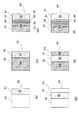
本発明の液晶表示素子では図2に示すように、1画素50を複数の副画素51,52(、53)に分割し、そのうちの1つの副画素52には緑色のカラーフィルタを重ねる。残る副画素51(と53)は、リタデーションを調節して、黒から白に至る無彩色の輝度変化と、赤からマゼンタを経て青にいたるいずれかの色とを表示させる。
In the liquid crystal display element of the present invention, as shown in FIG. 2, one
すなわち、電圧印加によって液晶層のリタデーションを変化させて有彩色を表示する第1の副画素と、カラーフィルタを有し、電圧によって明度変化範囲でリタデーションを変化させて該カラーフィルタの色を表示する第2の副画素とで単位画素を構成する。視感度の高い緑色を表示させる画素には、ECBによる着色を利用しないで緑色のカラーフィルタGを用い、赤と青だけにECBによる着色現象を利用することが特徴である。 That is, it has a first subpixel that displays a chromatic color by changing the retardation of the liquid crystal layer by applying a voltage, and a color filter, and displays the color of the color filter by changing the retardation in the brightness change range by the voltage. A unit pixel is composed of the second sub-pixel. A feature of using a green color filter G without using ECB coloring for pixels that display green with high visibility is to use the ECB coloring phenomenon only for red and blue.
例えば,カラーフィルタのある緑(G)画素を暗状態とし、透明画素(以下,カラーフィルタのない画素をこう呼ぶ)を白色(無彩色変化領域の最大輝度状態)にすることにより、画素全体として白を表示することが出来る。 For example, a green (G) pixel with a color filter is set to a dark state, and a transparent pixel (hereinafter, a pixel without a color filter is referred to as this) is set to white (the maximum luminance state of an achromatic color change region), thereby making the entire pixel as a whole. White can be displayed.
あるいは、G画素を最大透過状態にし,透明画素を有彩色領域のマゼンタ色にしてもよい。マゼンタ色は赤(R)と青(B)の両方の色を含むので、合成の結果白表示が得られる。 Alternatively, the G pixel may be set to the maximum transmission state, and the transparent pixel may be set to magenta in the chromatic color region. Since the magenta color includes both red (R) and blue (B) colors, white display is obtained as a result of synthesis.
G単色にするには、G画素を最大透過状態にし,透明画素を暗状態にする。R単色(B単色)にするには、G画素を暗状態にし,透明画素のリタデーション値を450nm(600nm)にする。組み合わせることでRとG、BとGの混色も得られる。 In order to obtain a single G color, the G pixel is set to the maximum transmission state and the transparent pixel is set to the dark state. In order to obtain an R single color (B single color), the G pixel is set in a dark state, and the retardation value of the transparent pixel is set to 450 nm (600 nm). By combining them, it is possible to obtain a mixed color of R and G and B and G.
G画素と透明画素をともにリタデーションを0にして暗状態とすれば黒表示が得られことはいうまでもない。 Needless to say, a black display can be obtained by setting the retardation of the G pixel and the transparent pixel to 0 and making them dark.
本発明の構成では,G画素はリタデーションを0から250nmの範囲で変化させ,透明画素はリタデーションを0から250nmの範囲と450nmから600nmの範囲で変化させる。通常は液晶材料は両副画素で共通にするので、駆動電圧範囲を異なるように設定する。 In the configuration of the present invention, the G pixel changes the retardation in the range of 0 to 250 nm, and the transparent pixel changes the retardation in the range of 0 to 250 nm and the range of 450 nm to 600 nm. Usually, since the liquid crystal material is common to both sub-pixels, the driving voltage range is set to be different.
カラーフィルタを緑色に選んだ結果,緑をリタデーションの調節で作ることが回避されてセル厚を大きくする必要がない。また,緑色は視感度が高いので、カラーフィルタによって純度の高い色を作ることにより、画質が向上する。 As a result of selecting the color filter as green, it is avoided that green is produced by adjusting the retardation, and there is no need to increase the cell thickness. In addition, since green has high visibility, the image quality is improved by producing a high-purity color with a color filter.
本発明の特徴は上記のようにG画素をカラーフィルタで表示し,その他の色を媒体(上の場合は液晶)自身が発生させる色で表示するもので,液晶以外にも適用できる。すなわち,一般に,外部から加えられる変調手段によって光学的性質を変化させる媒体を用い、その媒体が、変調手段によって明度を変化させる変調領域と、色相を変化させる変調領域とを有するものであれば本発明が適用できる。 The feature of the present invention is that the G pixel is displayed by the color filter as described above, and other colors are displayed by colors generated by the medium (in the above case, the liquid crystal) itself, and can be applied to other than the liquid crystal. That is, in general, if a medium whose optical properties are changed by a modulation means applied from the outside is used and the medium has a modulation area whose brightness is changed by the modulation means and a modulation area whose hue is changed, this medium is used. The invention can be applied.
具体的な媒体の例は以下で説明するが,そのような媒体を用いて表示素子を構成し,単位画素を、透明な第1の副画素と、カラーフィルタを有する第2の副画素で構成し、第1の副画素に色相が所定の範囲で変化するような変調を与えてその範囲の色を表示させ、第2の副画素に明度変化範囲の変調を与えてカラーフィルタの色の明るさ変化させる。黒,灰色,白の無彩色を表示するには、透明な第1の副画素に明度変化範囲の変調を与えればよい。 A specific example of the medium will be described below. A display element is configured using such a medium, and a unit pixel is configured by a transparent first subpixel and a second subpixel having a color filter. Then, the first subpixel is modulated such that the hue changes in a predetermined range to display the color in the range, and the second subpixel is modulated in the brightness change range to adjust the brightness of the color of the color filter. Change. In order to display black, gray, and white achromatic colors, it is only necessary to modulate the brightness change range to the transparent first subpixel.
本発明により通常用いられる液晶表示素子と比較してセル厚を極端に厚くする必要がなくなる。図1によると、赤はリタデーションが450nmであって、青はリタデーションが600nmである。したがって、600nmのリタデーションを実現するためのセル厚に設定すればよいことになる。上記例で言うと、セル厚は約10ミクロンでよいことになる。この程度であれば、応答速度の増加も小さく、約150ミリ秒程度となり、若干のボケは存在するものの動画表示が可能となる。 According to the present invention, it is not necessary to make the cell thickness extremely thick as compared with the liquid crystal display element normally used. According to FIG. 1, red has a retardation of 450 nm and blue has a retardation of 600 nm. Therefore, it is sufficient to set the cell thickness to realize 600 nm retardation. In the above example, the cell thickness may be about 10 microns. At this level, the increase in response speed is small, about 150 milliseconds, and a moving image can be displayed although there is a slight blur.
またこれを反射型液晶表示素子に適用した場合には、セル厚が半分となるため応答速度はこの1/4の40ミリ秒以下となり、動画表示にもほぼ問題ないレベルにすることができる。 When this is applied to a reflective liquid crystal display element, the cell thickness is halved, so the response speed is 40 milliseconds or less of this 1/4, and it can be brought to a level with no problem for moving image display.
また緑の色再現範囲はカラーフィルタによって決まり、かつ視感度がたかいために、白色成分の透過率を犠牲にすることなく高い色再現性を実現することが可能となる。 Further, since the green color reproduction range is determined by the color filter and the visibility is high, high color reproducibility can be realized without sacrificing the transmittance of the white component.
また緑画素のセル厚d2は、透過型の場合λ/2条件、反射型の場合には、λ/4条件が表示できれば十分であるため、透明画素のセル厚d1よりも薄くすることができ、その結果緑の画素の応答速度を高めることが可能となった。 In addition, the cell thickness d2 of the green pixel can be made thinner than the cell thickness d1 of the transparent pixel because it is sufficient to display the λ / 2 condition for the transmission type and the λ / 4 condition for the reflection type. As a result, the response speed of the green pixel can be increased.
つまり本発明の素子に関しては、視感度特性の高い緑画素の応答速度が速くなることから、人間の目には高速で表示されるように感じることが出来る。さらに前記例におけるカラーフィルタのない画素では、電圧印加時にECBによる着色を利用しているため、赤や青の表示は高電圧で駆動されていることになる。このことから、赤や青色画素では高電圧駆動に起因する高速表示、緑画素ではセル厚d2が薄い分だけ応答速度が速くなり、応答速度の色間ばらつきを抑制することも可能となる。 That is, regarding the element of the present invention, the response speed of green pixels with high visibility characteristics is increased, so that the human eye can feel that it is displayed at high speed. Further, in the pixel without the color filter in the above example, since the coloration by ECB is used at the time of voltage application, the display of red or blue is driven by a high voltage. Therefore, the red and blue pixels have a high-speed display resulting from high voltage driving, and the green pixel has a faster response speed corresponding to the smaller cell thickness d2 and can suppress variations in response speed between colors.
(階調表示)
図2(a)の液晶表示素子では、視感度特性の高い緑画素については連続階調表示可能であるが、透明画素部分の有彩色状態つまり青と赤はECBによる着色を利用しているため階調表示はできない。
(Gradation display)
In the liquid crystal display element of FIG. 2A, continuous gradation display is possible for green pixels having high visibility characteristics, but the chromatic state of the transparent pixel portion, that is, blue and red, uses coloring by ECB. Gray scale display is not possible.
図2(b)はこの点を改良するもので,透明画素は複数のサブピクセル51,53に分割し、その面積比を変えることによってデジタル的に階調を表現する。
FIG. 2B improves this point. The transparent pixel is divided into a plurality of
サブピクセルは異なる面積を有しているので、点灯して色が表示されるサブピクセルの面積によっていくつかの段階の中間調が表示される。 Since the sub-pixels have different areas, halftones of several levels are displayed depending on the area of the sub-pixel that is lit to display the color.
このとき前記サブピクセルがN個あったとき、その面積比を1:2:・・・:2N−1となるよう分割することで、リニアリティーの高い階調表示特性を得ることが出来る。図2(b)の例ではN=2としている。 At this time, when there are N subpixels, by dividing the area ratio to be 1: 2:...: 2 N−1 , it is possible to obtain gradation display characteristics with high linearity. In the example of FIG. 2B, N = 2.
本発明の液晶表示素子では視感度特性の低い赤と青にのみデジタル階調を使用している。緑画素には0から250nmの範囲で連続的な変調を与えることにより連続的な階調が表示できる。そのために、人間の目には、階調性が大きく損なわれたようには感じられず、比較的良好なカラー画像を得ることができる。すなわち目の検知しうる階調数が少ない赤と青に限ってデジタル階調を使用することで、限られた階調数でも十分な特性を持たせることが可能となるのも本発明の特徴である。 The liquid crystal display element of the present invention uses digital gradation only for red and blue, which have low visibility characteristics. Continuous gradation can be displayed on the green pixel by applying continuous modulation in the range of 0 to 250 nm. Therefore, the human eye does not feel that the gradation is greatly impaired, and a relatively good color image can be obtained. That is, by using digital gradation only for red and blue, which have a small number of gradations that can be detected by the eyes, it is possible to provide sufficient characteristics even with a limited number of gradations. It is.
なお上記のように限られた階調数でも十分な階調性を感じさせるためにも、画素ピッチは細かい方が好ましい。つまり、人間が画素を識別できなくなる解像度という観点で、200ミクロンピッチ以下にしておくことがより望ましい。 It should be noted that the pixel pitch is preferably fine so that sufficient gradation can be felt even with a limited number of gradations as described above. That is, it is more desirable to set the pitch to 200 microns or less from the viewpoint of resolution at which humans cannot identify pixels.
(応用例)
以上述べたように、本発明の液晶表示素子は、赤、青色についてはECB効果に基づく着色現象を利用した表示方法をとるので、赤色と青色それぞれのカラーフィルタを使用する場合と比較して光ロスを大幅に減少させることができる。その結果、従来のRGBカラーフィルタのみによって三原色を表示する方式と比べて光利用効率の高い素子が得られることが特長である。よって本発明の液晶表示素子を反射型液晶表示素子として、ペーパーライクディスプレイまたは電子ペーパーに用いることが出来る。
(Application examples)
As described above, since the liquid crystal display element of the present invention adopts a display method using a coloring phenomenon based on the ECB effect for red and blue, it is light compared with the case of using red and blue color filters. Loss can be greatly reduced. As a result, it is a feature that an element with high light utilization efficiency can be obtained as compared with the conventional method of displaying the three primary colors using only the RGB color filter. Therefore, the liquid crystal display element of the present invention can be used as a reflective liquid crystal display element in a paper-like display or electronic paper.
一方、本モードは透過型液晶表示素子としても、液晶層の透過率が高いので、従来方式のものと同一の輝度を得るために必要なバックライト消費電力が少なくて済み、低消費電力化という観点から好適に用いられる。 On the other hand, since this mode has a high transmittance of the liquid crystal layer even as a transmissive liquid crystal display element, less backlight power consumption is required to obtain the same brightness as that of the conventional method, which means lower power consumption. It is preferably used from the viewpoint.
さらに,高速な液晶応答性があるので,本発明の表示素子は動画表示にも用いることが出来る。従来、テレビ用途の液晶表示素子に関して、鮮明な動画特性を実現するために、1フレーム期間内でバックライトの消灯期間を設ける『擬似インパルス駆動』と称されている駆動方法が特開2001−272956号公報などに提案されているが、消灯期間を設ける分だけの輝度低下が生じてしまうのが課題となっている。こうした用途に対しても本モードのように応答速度が速く、かつ透過率の高い表示素子を適用することが出来る。 Furthermore, because of the high-speed liquid crystal response, the display element of the present invention can also be used for displaying moving images. Conventionally, for a liquid crystal display element for television use, a driving method called “pseudo-impulse driving” in which a backlight extinguishing period is provided within one frame period in order to realize clear moving image characteristics is disclosed in JP-A-2001-272958. Although it has been proposed in Japanese Patent Publication No. Gazette and the like, the problem is that the luminance is reduced by the amount of time for which the extinction period is provided. For such applications, a display element having a high response speed and a high transmittance can be applied as in this mode.
また高い光利用効率が求められる投射型表示素子にも好適に用いられる。 Further, it is also suitably used for a projection display element that requires high light utilization efficiency.
(変形例)
以上述べた例では、緑色表示に関してはカラーフィルタを用いることによってアナログ階調を実現し、赤・青色についてはECB効果に基づく着色現象の利用および画素分割手法に基づく表示方法によって、赤色および青色表示の際にデジタル階調を実現した例を説明した。この例では、赤・青表示に対して限られた階調数でも十分な階調性を感じさせるためにも、高精細表示素子用途において、より好適に用いられる。
(Modification)
In the example described above, analog gradation is realized by using a color filter for green display, and red and blue are displayed for red and blue by using a coloring phenomenon based on the ECB effect and a display method based on a pixel division method. The example in which the digital gradation is realized at the time is described. In this example, it is more preferably used in high-definition display element applications in order to make a sufficient gradation even with a limited number of gradations for red / blue display.
一方、前述のような反射型液晶表示素子において、高い反射率でかつより多くの表示色が要求される用途も存在する。また、既にフルカラー表示可能な透過型液晶表示素子において、フルカラー表示能は維持したままバックライトの消費電力を抑制するために高い透過率の表示モードに対する要求もある。この他にも、高い光利用効率を有する液晶プロジェクターなど、フルカラー表示可能であってかつ光利用効率の高い表示モードに対する要求は非常に多く存在する。 On the other hand, in the reflection type liquid crystal display element as described above, there is an application that requires a high reflectance and more display colors. In addition, in a transmissive liquid crystal display element capable of full color display, there is a demand for a display mode with high transmittance in order to suppress power consumption of the backlight while maintaining full color display capability. In addition to this, there is a great demand for a display mode capable of full color display and having high light utilization efficiency, such as a liquid crystal projector having high light utilization efficiency.
このような要求にこたえるため、前記説明した本モードを基本とし、さらに多色化できる手法として
(1) ECB効果による着色現象を赤色・青色以外のリタデーション値においても利用する方法
(2) 緑と補色関係にあるカラーフィルタが配設されている画素の低リタデーション領域の連続階調色を利用する方法
(3) 赤色・青色の少なくともいずれか一方のカラーフィルタが配設された画素を追加する方法
がある。以下で、それぞれの方法について説明する。
In order to meet such demands, the above-described mode is used as a basis, and as a technique for further multi-coloring, (1) a method of using the coloring phenomenon due to the ECB effect even in retardation values other than red and blue (2) green and Method of using continuous tone color in low retardation region of pixels in which color filters having complementary colors are arranged (3) Method of adding pixels in which at least one of red and blue color filters is arranged There is. Hereinafter, each method will be described.
(変形例1)
ECB効果による着色現象を赤色・青色以外のリタデーション値においても利用する方法
上記説明中ではECB効果による着色現象を利用して赤色・青色表示を行う原理について説明した。このECB効果による着色現象では図9に示すように白色から青色に至るまで連続的に色調を変化させることができている。つまり、上記説明で述べた赤色・青色表示以外にも使用可能な表示色は多く存在しており、こうした表示色を用いることで上記説明よりも多くの表示色を表現することが可能となる。
(Modification 1)
Method of using coloring phenomenon due to ECB effect even in retardation values other than red / blue In the above description, the principle of performing red / blue display using coloring phenomenon due to ECB effect has been described. In the coloring phenomenon due to the ECB effect, the color tone can be continuously changed from white to blue as shown in FIG. That is, there are many display colors that can be used in addition to the red / blue display described in the above description. By using such display colors, it is possible to express more display colors than in the above description.
具体的には、前記第1の副画素にカラーフィルタが配設されていない構成において上記クロスニコル下での表示色変化に関して説明すると、図9中の矢印で示すように、リタデーション量がゼロから増加するにつれて黒色表示から灰色(中間調)を経て白色表示に至るような無彩色での明度変化が生じ、白色領域を超えたリタデーション量の範囲では、黄色→黄赤→赤→赤紫→紫→青紫→青色、というように様々な有彩色を連続的に変化させることができる。 Specifically, the display color change under the crossed Nicols in the configuration in which no color filter is disposed in the first subpixel will be described. As shown by the arrow in FIG. As it increases, the brightness changes in achromatic color from black display to gray (halftone) to white display, and in the range of retardation beyond the white area, yellow → yellow red → red → red purple → purple → Various chromatic colors such as blue-purple → blue can be continuously changed.
無彩色領域と緑画素と組み合わせることにより、明るいグリーンディスプレイを構成することも出来る。また、有彩色領域の色と緑画素を組み合わせて中間色を表示してもよい。 A bright green display can be constructed by combining an achromatic region and a green pixel. Further, an intermediate color may be displayed by combining the color of the chromatic color region and the green pixel.
またこれらの有彩色は、上記構成によって赤色・青色と同様にデジタル階調を表現することが可能となる。これによって更に多くの表示色を表現することが可能となる。 In addition, these chromatic colors can express digital gradation in the same manner as in the red and blue colors. As a result, more display colors can be expressed.
(変形例2)
緑と補色関係にあるカラーフィルタが配設されている画素の低リタデーション領域の連続階調色を利用する方法
上記基本形態や変形例1のように前記第1の副画素にカラーフィルタを用いない場合には、白色領域を超えたリタデーション量の範囲では、黄色→黄赤→赤→赤紫(マゼンタ)→紫→青紫→青色という色調変化を示す。本変形例は、リタデーション変化で着色するほうの第1の副画素にマゼンタなどの緑色と補色の関係にあるカラーフィルタを配設するものである。これによって赤色および青色の色再現範囲を大幅に広げることが可能となる。
(Modification 2)
A method using a continuous tone color in a low retardation region of a pixel in which a color filter having a complementary color relationship with green is used. A color filter is not used for the first sub-pixel as in the basic mode and the first modification. In this case, in the range of the retardation amount exceeding the white region, the color tone changes from yellow → yellow red → red → red purple (magenta) → purple → blue purple → blue. In this modification, a color filter having a complementary color relationship with green, such as magenta, is disposed in the first sub-pixel that is colored by changing the retardation. As a result, the color reproduction range of red and blue can be greatly expanded.
図2(c)と(d)は本変形例の画素構成を示す。G画素51には基本形態と同じく緑のカラーフィルタが配設されており、基本形態および変形例1では透明であった第1の副画素(52、53)にマゼンタ色のカラーフィルタが配設されている。図2(c)が第1の副画素が1つ(52)の場合、(d)が第1の副画素を2:1の2つ(52,53)に分割した場合である。
2C and 2D show the pixel configuration of this modification. The
第2の副画素(G画素)51には、上記基本形態と同じく明度を変化させる変調領域の変調を与えて緑色の明度を変化させ,第1の副画素(52,53)には、色相を変化させる変調領域の変調を与えて有彩色を表示させるとともに、前記明度を変化させる変調領域の変調を与えてマゼンタ色の明度を変化させる表示を行う。 The second sub-pixel (G pixel) 51 is modulated in the modulation region that changes the lightness as in the above basic form to change the green lightness, and the first sub-pixel (52, 53) has a hue. A chromatic color is displayed by applying modulation in a modulation region that changes the brightness, and a display in which the brightness of the magenta color is changed by applying modulation in the modulation region that changes the brightness.
図10に、波長480nm〜580nmまでの透過率がゼロであり、それ以外の波長の透過率が100%となるような理想的なマゼンタカラーフィルタを配設した場合のリタデーションによる色変化の計算値を示す。リタデーション量がゼロから増加するにつれて黒色表示から暗いマゼンタ色(マゼンタ色の中間調)を経て明るいマゼンタ色表示に至るような有彩色での明度変化を示す。その後リタデーション量が更に増加し、前記第1の副画素にカラーフィルタを用いない例での白色領域を超えたリタデーション量の範囲になったときに、マゼンタ→赤→赤紫(マゼンタ)→紫→青色、というような有彩色の連続的変化を示す。 FIG. 10 shows the calculated value of the color change due to retardation in the case where an ideal magenta color filter in which the transmittance from the wavelength 480 nm to 580 nm is zero and the transmittance at other wavelengths is 100% is arranged. Indicates. As the retardation amount increases from zero, the brightness change in a chromatic color from black display to dark magenta (magenta halftone) to bright magenta display is shown. Thereafter, when the retardation amount further increases and the retardation amount exceeds the white region in the example in which no color filter is used for the first subpixel, magenta → red → red purple (magenta) → purple → It shows a continuous change of chromatic color such as blue.
図9と比較してみると,色度変化の範囲が赤と青の純色(色度図の隅)近くにまで広がっており,マゼンタカラーフィルタを配設することによって赤と青の色再現範囲が広がっていることがわかる。また,赤から青への変化が色度図の下辺に沿って動くので,赤から青への連続的な混色の変化が得られることもわかる。このように、マゼンタカラーフィルタを配設することによって赤と青の色再現範囲が広がると同時に、リタデーション変化したときに中間色の連続的変化も得られる。 Compared with FIG. 9, the range of chromaticity change extends to the vicinity of pure red and blue colors (the corners of the chromaticity diagram), and the red and blue color reproduction range by arranging a magenta color filter. It can be seen that is spreading. It can also be seen that since the change from red to blue moves along the lower side of the chromaticity diagram, a continuous color change from red to blue can be obtained. As described above, by arranging the magenta color filter, the color reproduction range of red and blue is expanded, and at the same time, a continuous change of the intermediate color is obtained when the retardation is changed.
本実施形態で白色を表示するには、マゼンタ画素52,53(本実施形態では、第1の副画素をこう呼ぶ)とG画素51をともに最大透過率を与える同じリタデーション値(250nm)に設定する。あるいは、G画素51を最大透過率状態(リタデーション値250nm)にし,マゼンタ画素52,53を赤と青の中間のリタデーション値(550nm付近)に設定してもよい。前者の方法の場合、無彩色の明度を変化させるには、両副画素の階調がそろって変化するように、マゼンタ画素のリタデーションを緑色のカラーフィルタ画素のリタデーションに合わせて変化させればよい。
In order to display white in the present embodiment, both the
黒表示,G・R・Bの各単色を表示する場合、それらの混色を表示する場合は、基本形態と同じである。 When displaying each color of black, G, R, and B, displaying the mixed color is the same as the basic mode.
マゼンタ画素が2つに分割されているときの階調表現は基本形態の図2(b)と同様である。 The gradation expression when the magenta pixel is divided into two is the same as in FIG. 2B of the basic form.
本変形例のように、マゼンタ色など緑色と補色関係にあるカラーフィルタを用いることによって、無彩色の階調表現ができると同時に、緑の補色の階調表現ができることから、表現できる表示色数を大幅に増加させることができる。 By using a color filter that has a complementary color relationship with green, such as magenta, as shown in this modification, it is possible to express gradations of achromatic colors and at the same time express gradations of complementary colors of green. Can be greatly increased.
また,マゼンタカラーフィルタは赤色と青色の両方を透過するので,従来の赤と青のカラーフィルタを併設する方式に比べて明るい表示が得られる。 In addition, since the magenta color filter transmits both red and blue, a bright display can be obtained as compared with the conventional method in which the red and blue color filters are provided.
(変形例3)
赤色・青色の少なくともいずれか一方のカラーフィルタが配設された画素を追加する方法
図2(e)は,本変形例の画素構成を示す。本変形例は,変形例2で説明したG画素51と(4:2:1の面積比で3分割されている)マゼンタ画素52,53,54に加えて,青のカラーフィルタをもつ第3の副画素55と赤のカラーフィルタをもつ第4の副画素56が付加されている。
(Modification 3)
Method for Adding Pixels with At least One of Red and Blue Color Filters FIG. 2E shows a pixel configuration of this modification. In this modification, in addition to the
G画素およびマゼンタ画素の表示作用は今までの実施形態と同じで,G画素は低リタデーション領域で変調されて緑の明るさを連続階調表示する。マゼンタ画素は,同じリタデーション領域で連続変調されるか,もしくはそれより大きい有彩色リタデーション領域で青色または赤色とその中間色を呈する。 The display operation of the G pixel and the magenta pixel is the same as that of the previous embodiments, and the G pixel is modulated in the low retardation region to display green brightness continuously. The magenta pixel is continuously modulated in the same retardation region, or exhibits blue or red and intermediate colors in a larger chromatic retardation region.
第3と第4の副画素55,56は、G画素と同じくリタデーションが0−250nmの範囲で変調され,青色と赤色の明るさが連続的に変化する。その役割を以下で説明する。
As with the G pixel, the third and
図11はRGB加法混色系において表示できる表示色を表しており、立法体中の任意の点はその座標値に対応した赤・青・緑の混色状態,Bkで示した頂点は明度が最小の状態を示している。ここで赤・緑・青の画像情報信号が与えられたときには、Bk点から延びるR・G・B独立ベクトルの和の位置に対応する表示色を表示することとなる。 FIG. 11 shows display colors that can be displayed in the RGB additive color mixture system. An arbitrary point in the cubic body is a mixed color state of red, blue, and green corresponding to the coordinate value, and a vertex indicated by Bk has the minimum brightness. Indicates the state. Here, when a red / green / blue image information signal is given, a display color corresponding to the position of the sum of the R, G, B independent vectors extending from the point Bk is displayed.
図中のR・G・Bはそれぞれ赤・緑・青の最大明度の状態を示しており、Wは最大明度の白色表示状態である。なお一辺の長さは255とした。 In the figure, R, G, and B indicate the maximum brightness states of red, green, and blue, respectively, and W indicates the maximum brightness white display state. The length of one side was 255.
ここで本発明の表示素子では、緑色に関してはカラーフィルタを用いた連続階調表示することを特徴としているために、緑方向には独立に任意の点を取ることができる。したがって、これ以降で表示色を議論するときには、赤・青ベクトルで構成される平面(以下RB平面と記載)上にて議論する。 Here, since the display element of the present invention is characterized by displaying continuous gradation using a color filter for green, an arbitrary point can be taken independently in the green direction. Therefore, when discussing the display color in the following, it is discussed on a plane composed of red and blue vectors (hereinafter referred to as RB plane).
まず、ECB効果に基づく着色現象を利用する画素が一つの場合(画素分割していない場合)について図12を用いて説明する。図12はRB平面を表している。ここで、赤表示および青表示時はECB効果に基づく着色現象を利用しており、明暗の表示状態として取り得るのはオンとオフの2値となる。したがって、R、Bそれぞれの軸上で取り得るのは最大値(R,B)と最小値(Bk)の2点である。 First, the case where there is one pixel using the coloring phenomenon based on the ECB effect (when pixel division is not performed) will be described with reference to FIG. FIG. 12 shows the RB plane. Here, at the time of red display and blue display, a coloring phenomenon based on the ECB effect is used, and the light and dark display states can be two values, on and off. Therefore, the maximum value (R, B) and the minimum value (Bk) can be taken on the R and B axes.
一方、(変形例2)で述べた構成、すなわち緑色と補色の関係にあるマゼンタカラーフィルタが設けられている場合は、マゼンタ画素のリタデーションを0−250nmの範囲で変化させることによりマゼンタ色の明るさを変化させることが出来る。この範囲の表示色はRB平面上では図12中で矢印で示したRとBの合成ベクトル方向の軸上にあり、連続的な明度変化を示すことに対応している。つまり(変形例2)では、図12の中ではBk点(原点)、R点、B点、および矢印上の任意の点が表示色として使用できることになる。 On the other hand, when the configuration described in (Modification 2), that is, when a magenta color filter having a complementary relationship with green is provided, magenta brightness is changed by changing the magenta pixel retardation in the range of 0 to 250 nm. You can change the height. The display color of this range is on the axis of the combined vector direction of R and B indicated by the arrow in FIG. 12 on the RB plane, and corresponds to the continuous change in brightness. That is, in (Modification 2), Bk point (origin), R point, B point, and any point on the arrow in FIG. 12 can be used as display colors.
次いで、ECB効果に基づく着色現象を利用する画素を1:2の比率で画素分割している場合について図13に記載のRB平面を用いて説明する。ここでも画素分割しない場合と同様に、赤表示および青表示時はECB効果に基づく着色現象を利用しているため、画素分割した各画素単独では明暗の表示状態として取り得るのはオンとオフの2値となる。一方、1:2の割合で二つの画素に分割しているために、R、Bそれぞれの軸上で取り得るのは図中の丸印で示した4点をとることができる。 Next, a case where a pixel using a coloring phenomenon based on the ECB effect is divided into pixels at a ratio of 1: 2 will be described using the RB plane shown in FIG. Here again, as in the case of no pixel division, since the coloring phenomenon based on the ECB effect is used at the time of red display and blue display, each pixel that has been divided into pixels can take on and off as a bright and dark display state. It becomes binary. On the other hand, since the pixel is divided into two pixels at a ratio of 1: 2, four points indicated by circles in the figure can be taken on the R and B axes.
ここで、図中のR3およびB3で示した点は、それぞれ二つの画素ともに赤表示もしくは青表示の状態である。 Here, the points indicated by R3 and B3 in the drawing are in a red display state or a blue display state for each of the two pixels.
R1およびB1で示した点は、画素分割したうちで小さい方の画素が赤表示もしくは青表示状態となっており、残りの大きい方の画素は黒表示状態である。ここで、大きい方の画素はマゼンタの連続階調色が取りうるので、R1およびB1それぞれの点からRB合成ベクトル方向に延びる矢印上の任意の点を取ることができる。同様の議論により、R2およびB2それぞれの点からRB合成ベクトル方向に延びる矢印上の任意の点を取ることができる。 Regarding the points indicated by R1 and B1, the smaller pixel among the divided pixels is in a red display state or a blue display state, and the remaining larger pixel is in a black display state. Here, since the larger pixel can take magenta continuous tone color, any point on the arrow extending from the respective points R1 and B1 in the RB composite vector direction can be taken. By the same argument, it is possible to take any point on the arrow extending in the direction of the RB composite vector from the respective points R2 and B2.
すなわち、マゼンタカラーフィルタのある第1の副画素を、異なる面積を有する2つのサブピクセルに分割して、一方のサブピクセルに赤,または青の有彩色を表示させ、もう一方のサブピクセルに明度を変化させる表示を行わせることによってマゼンタ色のデジタル中間調を表示する。緑画素は明度を連続的に変化させることができるので,この方法によりカラー表示ができる。 That is, a first subpixel having a magenta color filter is divided into two subpixels having different areas, one of the subpixels is displayed with a chromatic color of red or blue, and the other subpixel is displayed with lightness. A magenta digital halftone is displayed by causing the display to change. Since the brightness of the green pixel can be continuously changed, color display can be performed by this method.
同様の議論によって、ECB効果に基づく着色現象を利用する画素を1:2:4の比率で画素分割している場合に、取り得る表示色を図14中の矢印にて記載した。 According to the same argument, the possible display colors are indicated by arrows in FIG. 14 when a pixel using a coloring phenomenon based on the ECB effect is divided at a ratio of 1: 2: 4.
一般に,第1の副画素(ECB効果に基づく着色現象を利用する副画素)にマゼンタカラーフィルタを配置し,それを異なる面積を有する複数のサブピクセルに分割して、一部のサブピクセルにECB効果による赤,または青を表示させ、残りのサブピクセルに明度を変化させる表示を行わせることによってマゼンタ色のデジタル中間調を表示することができる。 In general, a magenta color filter is arranged in a first sub-pixel (a sub-pixel using a coloring phenomenon based on the ECB effect), and is divided into a plurality of sub-pixels having different areas, and an ECB is divided into some sub-pixels. A magenta digital halftone can be displayed by displaying red or blue depending on the effect and causing the remaining sub-pixels to change the brightness.
このように画素分割数を増やせば増やすほどRB平面上での取り得る表示色は増えていく。しかしこの手法はあくまでもデジタル階調であり、アナログフルカラー表示ではない。そこで、アナログ階調を得るためには赤色と青色のカラーフィルタを有する画素(図2(e)の55,56)を追加する。これらの画素は,それぞれ青と赤の連続的な明るさ変化を作るので、図13,14の上では,B軸方向とR軸方向の大きさ可変のベクトルで表される。これによって、赤色、青色の連続階調を表示することが出来るために、図13や図14において矢印上以外の部分を補完することが可能となり、RB平面上の全ての点を表現することが可能となる。 In this way, as the number of pixel divisions increases, the display colors that can be taken on the RB plane increase. However, this method is only a digital gradation and not an analog full color display. Therefore, in order to obtain an analog gradation, pixels (55 and 56 in FIG. 2E) having red and blue color filters are added. Since these pixels make continuous brightness changes of blue and red, respectively, in FIGS. 13 and 14, they are represented by vectors of variable sizes in the B-axis direction and the R-axis direction. As a result, red and blue continuous gradations can be displayed, so that it is possible to complement the portions other than those on the arrows in FIGS. 13 and 14 and express all points on the RB plane. It becomes possible.
すなわち,第2の副画素(明度変調のみの副画素)を複数の副画素に分割し、そのうちの1つに緑色カラーフィルタ、他に赤色と青色のカラーフィルタを配設する。この第2の各々の副画素に明度が変化する領域の変調を与えて明度変化を生じさせることにより、上で説明したマゼンタのデジタル中間調表示に連続階調が付加されて,RB平面の任意の中間調が表示でき,これに緑色の連続階調を組み合わせることにより,フルカラーが表示できる。 That is, the second sub-pixel (sub-pixel only for brightness modulation) is divided into a plurality of sub-pixels, one of which is provided with a green color filter and the other is provided with red and blue color filters. The second sub-pixel is modulated in a region in which the lightness changes to generate a lightness change, thereby adding a continuous tone to the magenta digital halftone display described above, so that an arbitrary RB plane can be obtained. Halftones can be displayed, and by combining this with a green continuous tone, full color can be displayed.
第2の副画素のうちの赤色と青色のカラーフィルタを配設した画素は,第1の副画素によって表示されるマゼンタ色のデジタル階調の隙間を埋めるのであるから,最大明度が、前記第1の副画素を構成するサブピクセルのうち最小のサブピクセルによって表示される明度と略一致するように変調を行えばよい。 Among the second sub-pixels, the pixel provided with the red and blue color filters fills the gap between the magenta digital gradations displayed by the first sub-pixel. What is necessary is just to modulate so that it may correspond with the lightness displayed with the smallest subpixel among the subpixels which comprise 1 subpixel.
このとき追加する赤、青それぞれのカラーフィルタを有する画素55,56の大きさは、前記画素分割した副画素52,53,54のうち最小面積の副画素54と同等の面積を持てば十分である。つまり例えば図14において、丸印で示したBk点からR7およびB7までの表示可能な点は等間隔で並んでいる。その丸印からRB合成ベクトル方向に延びる矢印上の任意の点をとることが出来ている。そのような色を表示可能な構成に対して、画素分割した副画素のうち最小面積の副画素と同等の面積を持つ赤色と青色のカラーフィルタを有する画素55,56を追加することによって、図15中のR−CFおよびB−CFとして示した矢印上の任意の点を加法混色することができる。これによって、RB平面上の全ての点を表現することが可能となることから、完全なアナログフルカラー表示が出来ることになる。
The size of the
また、上記のとおり、追加する赤、青それぞれのカラーフィルタを有する画素の大きさは、前記画素分割した副画素のうち最小面積の副画素と同等の面積を持てば十分であるために、画素分割数を増やせば増やすほど、赤・青カラーフィルタを使用することによる光利用効率の減少の影響を減らすことが可能となる。つまり、ECB効果に基づく着色現象を利用した画素の分割数が多いほど高い光利用効率を実現することが可能となる。 In addition, as described above, the size of the pixel having the red and blue color filters to be added is sufficient if it has an area equivalent to the sub-pixel having the smallest area among the sub-pixels obtained by dividing the pixel. As the number of divisions increases, it becomes possible to reduce the influence of the decrease in light utilization efficiency due to the use of red / blue color filters. That is, as the number of divided pixels using the coloring phenomenon based on the ECB effect increases, higher light utilization efficiency can be realized.
なお、このとき必ずしも赤色と青色両方のカラーフィルタを追加しないでも有効な効果を得ることが可能である。図2(f)はその例で,赤色のカラーフィルタを持つ画素56だけがある。図16に、赤色のカラーフィルタのみを追加したときの表示可能な色範囲をハッチングした領域として示した。この図では、赤色方向は全ての色が表現可能だが、青色方向は表現できない表示色が存在する図となっている。しかし、人間の視感度特性は青色が最も鈍感であり、必要な階調数は最も少なくても良いと考えられている。したがって、このように赤色のみを追加することによってフルカラーに相当するような表示色を得ることができる。
At this time, an effective effect can be obtained without necessarily adding both red and blue color filters. FIG. 2 (f) is an example, and there is only a
また図16で示した構成と全く同じ構成ではあるが、基準となるBkの点を図15におけるR1位置にずらすことによって、全ての表示色を表現することが可能となる。なおこのとき、黒表示状態が若干赤みがかった表示色となるが、例えば反射型表示素子など透過型表示素子と比較してコントラストがさほどシビアに要求されない用途ではこのような手法も使用可能である。 Further, although the configuration is exactly the same as the configuration shown in FIG. 16, all display colors can be expressed by shifting the reference Bk point to the R1 position in FIG. At this time, the black display state is a slightly reddish display color. For example, such a method can be used in applications where contrast is not so severe as compared with a transmissive display element such as a reflective display element.
以上述べた手法によって、高い光利用効率を維持したまま、フルカラーもしくはそれに相当するような表示色を表現することが可能となる。 By the method described above, it is possible to express a full color or a display color corresponding to it while maintaining high light utilization efficiency.
(適用できる液晶表示モード)
本発明は以下に述べるいろいろな液晶表示モードに適用できる。
(Applicable liquid crystal display modes)
The present invention can be applied to various liquid crystal display modes described below.
上で述べたVAモードは,液晶層の液晶分子が電圧無印加時には基板面に略垂直に配向し、電圧印加時には略垂直の配向から傾斜してリタデーションを変化させる。 In the VA mode described above, the liquid crystal molecules of the liquid crystal layer are aligned substantially perpendicularly to the substrate surface when no voltage is applied, and change the retardation by tilting from the substantially vertical alignment when a voltage is applied.
OCB(Opically Compensated Bend)モードは、液晶層の液晶分子が電圧印加によってベンド配向と略垂直配向との間にて配向状態を変化させることでリタデーションを変化させるので、本発明を適用できることはVAモードと同様である。 In the OCB (Optically Compensated Bend) mode, the liquid crystal molecules in the liquid crystal layer change the retardation by changing the alignment state between the bend alignment and the substantially vertical alignment by applying a voltage, and therefore the present invention can be applied to the VA mode. It is the same.
本発明ではリタデーション変化による表示色を利用するために、視野角による色調変化を考慮しなければならない。しかし昨今のLCD開発の進歩は著しく、RGBカラーフィルタ方式を用いたカラー液晶ディスプレイでは視野角依存性の問題はほとんど解決しているといっても過言ではない。例えばOCBモードではベンド配向による自己補償効果によって、視野角の変化に伴うリタデーション変化を抑制することが報告されている。 In the present invention, in order to use the display color due to the retardation change, it is necessary to consider the color tone change due to the viewing angle. However, recent progress in LCD development is remarkable, and it is no exaggeration to say that the problem of viewing angle dependency is almost solved in color liquid crystal displays using the RGB color filter system. For example, in the OCB mode, it is reported that the retardation change accompanying the change in the viewing angle is suppressed by the self-compensation effect by the bend alignment.
また、STNモードも位相差フィルム開発の進展によって視野角特性は大きく改善されている。これらOCBやSTNモードもリタデーション量を適宜設定することによってECB効果に基づく着色現象を得ることができるため、本発明の構成を適用することが可能である。特にOCBモードでは、先に述べた応答速度に関して大幅に改善することが出来るために、高速性が必要となる用途では好適に用いられる。 In addition, the viewing angle characteristics of the STN mode are greatly improved due to the development of the retardation film. Since the OCB and STN modes can obtain a coloring phenomenon based on the ECB effect by appropriately setting the retardation amount, the configuration of the present invention can be applied. In particular, in the OCB mode, the response speed described above can be greatly improved. Therefore, the OCB mode is preferably used in applications that require high speed.
一方、MVA(Multidomain Virtical Alignment)モードは非常に良好な視野角特性を示すモードとして既に商品化され、広く使用されている。その他、PVA(Patterned Virtical Alignment)モードと称されるモードも広く使用されている。 On the other hand, the MVA (Multidomain Virtual Alignment) mode has already been commercialized and widely used as a mode exhibiting very good viewing angle characteristics. In addition, a mode called a PVA (Patterned Virtual Alignment) mode is also widely used.
これらの垂直配向モードは、表面に凹凸をつけたり(MVA)、電極形状を工夫したり(PVA)して電圧印加時の液晶分子傾斜方向を制御することで、広い視野角特性を実現している。そして、これらは電圧によってリタデーション量を変化させるモードであるために、本発明の構成を適用することが可能である。こうすることで高い透過率(もしくは反射率)、広い視野角、広い色空間を同時に満足する液晶表示素子を実現することが可能となる。 These vertical alignment modes achieve a wide viewing angle characteristic by controlling the liquid crystal molecule tilt direction during voltage application by making the surface uneven (MVA) or devising the electrode shape (PVA). . Since these are modes in which the amount of retardation is changed by voltage, the configuration of the present invention can be applied. By doing so, it is possible to realize a liquid crystal display element that simultaneously satisfies high transmittance (or reflectance), a wide viewing angle, and a wide color space.
なお、図3は本発明で用いる反射型液晶素子の構成を示すものであり、この反射型液晶素子は同図に示すように偏光板1、位相補償板2、ガラス基板3、透明電極4、液晶層5、透明電極6、反射板を表面に備えたガラス基板7を備えている。このときの明暗の表示が出来る原理について簡単に述べる。
FIG. 3 shows the configuration of a reflective liquid crystal element used in the present invention. As shown in the figure, the reflective liquid crystal element includes a
簡単のため用いる波長は550nm(単波長)のみとする。位相補償板2は一軸であり、そのリタデーション量は137.5nmとし、遅相軸が(偏光板1の偏光軸8から見て)時計回りに45度になるように配置されている。
For simplicity, the wavelength used is only 550 nm (single wavelength). The
液晶層5は電圧無印加時に垂直配向であり、電圧印加により分子が傾斜する、いわゆるVAモードであるとして説明を行う。液晶分子の傾斜方向は、位相補償板2の光軸と平行,すなわち偏光板1に対して(偏光板側の偏光軸8から見て)時計回りに45度とする。このときの様子を図4(a)に示す。なお、同図において、9は位相補償板2の光軸である。
The liquid crystal layer 5 will be described as being in a so-called VA mode in which the liquid crystal layer 5 is vertically aligned when no voltage is applied, and molecules are tilted when a voltage is applied. The tilt direction of the liquid crystal molecules is 45 degrees parallel to the optical axis of the
偏光板1を通過した外光は、位相補償板の光軸9方向の偏光成分と,それに垂直な偏光成分に分けられる。それぞれに成分は,位相補償板2と液晶層5を往復2回ずつ通過し,その結果両者に位相差が生じる。その値は,位相補償板のリタデーションと液晶層のリタデーションの和で与えられ,再び偏光板を通過して外に出てくる。
The external light that has passed through the
液晶層5に電圧が印加されていない場合には、垂直配向であるが故に、液晶層5のリタデーション値はゼロである。したがって、上記構成における反射率T%は以下の式で表される。 When no voltage is applied to the liquid crystal layer 5, the retardation value of the liquid crystal layer 5 is zero because of the vertical alignment. Therefore, the reflectance T% in the above configuration is expressed by the following equation.
T%=cos2(π×2×137.5/550)
=0 ・・・(式1)
T% = cos 2 (π × 2 × 137.5 / 550)
= 0 (Formula 1)
これにより、電圧無印加時の反射率はゼロ、すなわちいわゆるノーマリブラック構成ということになる。 Thus, the reflectance when no voltage is applied is zero, that is, a so-called normally black configuration.
次いで、電圧印加時について考える。 Next, consider the time of voltage application.
このとき電圧印加によって液晶分子は位相補償板2と平行な方向に傾斜する。したがって、液晶分子の傾斜によって液晶層5に発生するリタデーション量をR(V)とすると、電圧印加時の反射率T%(V)は以下の式で表される。
At this time, the liquid crystal molecules are inclined in a direction parallel to the
T%(V)=cos2(π×2×(137.5+R(V))/550)
・・・(式2)
T% (V) = cos 2 (π × 2 × (137.5 + R (V)) / 550)
... (Formula 2)
これにより電圧に応じた所望の反射率が得られることになる。
以上の説明では,液晶分子は位相補償板の光軸方向と平行に傾斜するとしたが,位相補償板を通過した光は円偏光となるので,液晶の分子の傾斜方向はそれに限らず任意の方向でよい。
Thereby, a desired reflectance according to the voltage is obtained.
In the above description, the liquid crystal molecules are inclined in parallel with the optical axis direction of the phase compensator. However, since the light passing through the phase compensator is circularly polarized, the tilt direction of the liquid crystal molecules is not limited to this and is arbitrary. It's okay.
また上記と同様の電圧無印加時に垂直配向状態をとる配向モードとしてCPA(Continuous Pinwheel Alignment)モードが提案されている。(シャープ技報:第80号・2001年8月 p.11参照) In addition, a CPA (Continuous Pinwheel Alignment) mode has been proposed as an alignment mode that takes a vertical alignment state when no voltage is applied, similar to the above. (See Sharp Technical Report: No. 80, August 2001, p. 11)
このモードも上記PVA方式と同様に、電極形状を工夫することによって電圧印加時の液晶分子の傾斜方向を制御する方式である。この方式では電圧印加時にはサブピクセル中心部から放射状に液晶分子が傾斜する配向状態となることで広視野角化を実現している。そして、このCPAモードについても電圧によってリタデーション量を変化させるモードであるために、本発明の構成を適用することが可能である。 Similar to the PVA method, this mode is a method of controlling the tilt direction of the liquid crystal molecules during voltage application by devising the electrode shape. In this method, when a voltage is applied, a wide viewing angle is realized by an alignment state in which liquid crystal molecules are inclined radially from the center of the subpixel. Since this CPA mode is also a mode in which the retardation amount is changed by the voltage, the configuration of the present invention can be applied.
なお、CPAモードにおいて、液晶の透過率を高めるためにカイラル材を添加した液晶材料を用いたリバースTN方式を用いることによって、複屈折性と旋光性を併用することが出来るために光利用効率が高くなる(上記文献参照)。このカイラル材添加についても、本発明の構成にて適用することが可能である。 Note that, in the CPA mode, by using the reverse TN method using a liquid crystal material to which a chiral material is added in order to increase the transmittance of the liquid crystal, the birefringence and the optical rotation can be used together. It becomes higher (see the above-mentioned document). This addition of chiral material can also be applied in the configuration of the present invention.
ただし、本発明の構成において、反射型液晶であってかつ円偏光板を使用する場合にはCPAモードにおいてカイラル材を添加しなくとも良好な反射率を得ることが可能である。これについて以下に説明する。 However, in the configuration of the present invention, when a reflective liquid crystal is used and a circularly polarizing plate is used, it is possible to obtain a good reflectance without adding a chiral material in the CPA mode. This will be described below.
(1)円偏光板、(2)液晶層、(3)反射板という3つの層が積層された構成を考える。まず液晶層に複屈折がない場合、例えば液晶層が垂直配向状態になっている場合には、外部からの入射光はまず(1)の円偏光板を通過し、偏光状態に変調を受けないまま反射し、その反射光は再び円偏光板を通過して外界に向かって光は進行する。 Consider a configuration in which three layers of (1) a circularly polarizing plate, (2) a liquid crystal layer, and (3) a reflector are laminated. First, when there is no birefringence in the liquid crystal layer, for example, when the liquid crystal layer is in a vertically aligned state, incident light from the outside first passes through the circularly polarizing plate of (1) and is not modulated by the polarization state. Reflected as it is, the reflected light passes through the circularly polarizing plate again, and the light travels toward the outside.
ここで、光は円偏光板を2回通過することになるために、特に円偏光条件を満たす波長領域では光が外界に出てくることは無い。つまり電圧無印加状態において垂直配向であるCPAモードは上記構成においてノーマリブラック構成である。ここで、電圧を印加した場合には放射状に液晶分子が傾斜することから、方位角方向に対して全ての方向に傾斜することになる。前記文献のように透過型であって液晶層に直線偏光が入射される場合には、液晶の分子軸方向と偏光板の偏光方向とが一致するときに光利用効率の低下につながるが、液晶層に対して円偏光が入射されるような構成の場合には、液晶が傾斜する分子軸方向によらずに等しく偏光が変調される。 Here, since the light passes through the circularly polarizing plate twice, the light does not come out to the outside especially in the wavelength region satisfying the circular polarization condition. That is, the CPA mode, which is vertically aligned in the state where no voltage is applied, has a normally black configuration in the above configuration. Here, when a voltage is applied, the liquid crystal molecules tilt radially, and therefore tilt in all directions with respect to the azimuth angle direction. When the linearly polarized light is incident on the liquid crystal layer as in the above document, the light use efficiency is reduced when the molecular axis direction of the liquid crystal coincides with the polarization direction of the polarizing plate. In the case where the circularly polarized light is incident on the layer, the polarized light is modulated equally regardless of the molecular axis direction in which the liquid crystal is tilted.
以上の原理によって、本発明の構成において円偏光板を用いた反射型表示モードであってCPAモードを適用する場合には、上記文献に記載のようにカイラル材を添加してもよいし、必ずしもカイラル材を添加しなくてもよい。
(半透過型液晶表示素子への適用)
Based on the above principle, when the CPA mode is applied in the reflective display mode using the circularly polarizing plate in the configuration of the present invention, a chiral material may be added as described in the above-mentioned document, It is not necessary to add a chiral material.
(Application to transflective liquid crystal display devices)
ところで、上記従来の技術の中で説明したが、半透過型液晶表示素子に使用される断面構成は透過部と反射部の光利用効率を両方とも最大化するために、透過部のセル厚を反射部のセル厚の2倍になるように層間絶縁膜を設ける構成となっており、これは公知となっている。 By the way, as explained in the above prior art, the cross-sectional configuration used in the transflective liquid crystal display element has a cell thickness of the transmissive part in order to maximize the light use efficiency of both the transmissive part and the reflective part. An interlayer insulating film is provided so as to be twice the cell thickness of the reflection portion, which is publicly known.
本発明の表示素子においても上記公知の構成を採用することは可能である。 The display device of the present invention can also employ the above known configuration.
しかし一方、本発明の表示素子において上記構成を実現しようとした場合、複屈折による着色を利用した表示原理に基づいているために、ツイステッドネマティック(TN)がた液晶素子など,それを用いない液晶表示素子よりも厚いセル厚が必要となる。つまり前記層間絶縁膜の厚みが通常の半透過型液晶表示素子と比べて大きい構成が必要とされる。 On the other hand, when the above-described configuration is to be realized in the display element of the present invention, since it is based on the display principle using coloring by birefringence, a liquid crystal element such as a twisted nematic (TN) liquid crystal element is not used. A cell thickness larger than that of the display element is required. That is, a configuration is required in which the thickness of the interlayer insulating film is larger than that of a normal transflective liquid crystal display element.
さらに半透過型液晶表示素子の利用状況を考えると、上記の通り、非常に明るい外光中でも十分な視認性をもって表示されることと、室内や暗所などにおいて高いコントラストや色再現性を実現し、フルカラーデジタルコンテンツを忠実に再現することが要求される。 Furthermore, considering the usage of transflective liquid crystal display elements, as described above, it is displayed with sufficient visibility even in very bright outside light, and it achieves high contrast and color reproducibility in indoor and dark places. Therefore, it is required to faithfully reproduce full-color digital content.
この中で、非常に明るい外光中でも十分な視認性をもって表示されることに関しては、本提案の複屈折による着色を利用した表示原理に基づく表示方法を反射型モードとして使用することによって可能である。 Among these, regarding display with sufficient visibility even in very bright outside light, it is possible to use the proposed display method based on the display principle using coloring by birefringence as a reflective mode. .
一方、本提案における基本的な構成として説明した方法では青や赤など緑以外の表示色は、ECB効果に基づく着色現象を利用した表示方法および画素の面積分割によるデジタル階調を採用しているが、こうしたデジタル階調は極めて高精細な表示素子においては人間の視認限以上となるため、完全なフルカラー表示に相当するが、精細度が必ずしも十分でない場合には階調表示能が若干不足して感じることがある。 On the other hand, in the method described as the basic configuration in the present proposal, the display colors other than green such as blue and red adopt a display method using a coloring phenomenon based on the ECB effect and digital gradation by pixel area division. However, since these digital gradations exceed the human visibility limit in extremely high-definition display elements, they correspond to complete full-color display, but if the definition is not sufficient, the gradation display capability is slightly insufficient. You may feel that.
したがって透過型モードにてフルカラーデジタルコンテンツを忠実に再現するためには、より高い階調表示能を有することが必要と考えられる。 Therefore, in order to faithfully reproduce full-color digital content in the transmission mode, it is considered necessary to have higher gradation display capability.
そこで本発明では透過モードではRGBのカラーフィルタを用い、液晶層は黒から白にかけて連続的に透過率を変化させるという、一般に用いられているマイクロカラーフィルタ方式を採用する。つまり反射モードはECB効果による着色を利用したモードによる赤および青表示とカラーフィルタによる緑表示、透過モードは赤・緑・青ともにカラーフィルタによるカラー表示とする。ことで、上記2つの半透過型液晶に要求される項目を両立することが可能となる。 Therefore, the present invention employs a commonly used micro color filter system in which RGB color filters are used in the transmission mode and the liquid crystal layer continuously changes its transmittance from black to white. That is, the reflection mode is red and blue display by a mode using coloring by the ECB effect and green display by a color filter, and the transmission mode is color display by a color filter for all red, green and blue. This makes it possible to satisfy both items required for the two transflective liquid crystals.
このような反射と透過で異なる表示モードによる素子構成を採用することによって、単なる組み合わせではない有効な効果が発現する。 By adopting such an element configuration with different display modes for reflection and transmission, an effective effect that is not just a combination is exhibited.
前記のとおり、現行の半透過型液晶表示素子では反射領域と透過領域で同じ原理に基づく表示方法を採用しているために、それぞれが最適な光利用効率を示すためには、反射領域と透過領域とで2倍のセル厚差を付与しなければならない。 As described above, the current transflective liquid crystal display element employs a display method based on the same principle in the reflective region and the transmissive region. The cell thickness difference between the regions must be doubled.
そのために上述のように層間絶縁膜形成プロセスが必要となっている。 Therefore, an interlayer insulating film forming process is necessary as described above.
一方、本提案のように反射と透過で異なる表示モード、特に反射モードにECB効果による着色を利用したモード、透過モードにはECB効果による着色を利用しないモードを採用した半透過型液晶表示素子の場合、ECB効果による着色を利用したモードにおいて、本発明では青表示までをECB効果で表現できれば良い。よって黒から青表示までを反射モードにおいて実現するためには、液晶層(あるいは液晶層と位相補償板の組み合わせ)によるリタデーション量が、電圧による制御により0nmから300nmの範囲で変化させることができればよい。 On the other hand, a transflective liquid crystal display element that employs different display modes for reflection and transmission as in the present proposal, particularly a mode that uses coloring by the ECB effect for the reflection mode, and a mode that does not use coloring by the ECB effect for the transmission mode. In this case, in the mode using coloring by the ECB effect, it is sufficient that the present invention can express up to blue display by the ECB effect. Therefore, in order to realize black to blue display in the reflection mode, the retardation amount by the liquid crystal layer (or the combination of the liquid crystal layer and the phase compensation plate) only needs to be able to be changed in the range of 0 nm to 300 nm by voltage control. .
一方、透過モードにおいて黒から白表示までをECB効果で実現するためには、液晶層(あるいは液晶層と位相補償板の組み合わせ)によるリタデーション量が電圧による制御により0nmから250nm程度の範囲で変化させることができればよい。 On the other hand, in order to realize black to white display in the transmission mode by the ECB effect, the retardation amount by the liquid crystal layer (or a combination of the liquid crystal layer and the phase compensation plate) is changed in the range of about 0 nm to 250 nm by voltage control. I can do it.
つまり、反射領域において必要とされるセル厚と透過領域において必要とされるセル厚とが非常に近いことになる。したがって、現行の構成と比較すると前記層間絶縁膜の厚みを大幅に減少させることが可能となる。これによって、セル厚差を付けた結果発生しがちな配向欠陥や、段差部のテーパーに起因する開口率の減少を抑制することが可能となる。 That is, the cell thickness required in the reflection region and the cell thickness required in the transmission region are very close. Therefore, the thickness of the interlayer insulating film can be greatly reduced as compared with the current configuration. As a result, it is possible to suppress a decrease in the aperture ratio due to alignment defects that tend to occur as a result of the cell thickness difference and the taper of the stepped portion.
あるいは液晶層厚を300nmまでの制御が可能な条件で一定にしておき、透過モードにおける電圧による制御範囲を0nmから250nmに限定するようにすれば、前記層間絶縁膜を形成しなくても良いことになる。これによりフォトリソグラフィープロセスの簡略化が実現でき、コストダウンに寄与できる。また均一配向実現が容易となり、かつ開口率の向上にも寄与することができる。 Alternatively, if the thickness of the liquid crystal layer is kept constant under conditions that allow control up to 300 nm, and the control range by the voltage in the transmission mode is limited to 0 nm to 250 nm, the interlayer insulating film need not be formed. become. Thereby, simplification of the photolithography process can be realized, which can contribute to cost reduction. Further, uniform alignment can be easily realized, and it can contribute to an improvement in aperture ratio.
なお本発明の半透過型液晶表示素子では同一電圧印加条件にて反射モードと透過モードで表示させた場合に、それぞれの表示色が異なってしまう可能性がある。この場合、反射領域と透過領域とで独立に印加電圧が制御できるような画素構成にしておくことがより好ましい。 In the transflective liquid crystal display element of the present invention, when the display is performed in the reflection mode and the transmission mode under the same voltage application condition, the display colors may be different. In this case, it is more preferable that the pixel configuration be such that the applied voltage can be controlled independently between the reflective region and the transmissive region.
以上の議論をまとめ、本発明の半透過型液晶表示素子として好ましい構成を例示したものを図6に示す。 FIG. 6 shows a summary of the above discussion and an example of a preferable configuration as the transflective liquid crystal display element of the present invention.
図6に示した61,62,63はITOによる透明電極である。この透明電極61,62,63を通過する光の光路上にはそれぞれ青・緑・赤のカラーフィルタが形成されている。64,65,66はアルミなどによる反射電極である。65の反射電極で反射する光の光路上には緑のカラーフィルタが形成されている。
このカラーフィルタは光利用効率を高めるために、色再現範囲の狭い反射型タイプのものを用いることもできるし、あるいは62に用いる透過型用カラーフィルタを反射電極の一部だけに形成させることもできる。64、66の反射電極上にはカラーフィルタを形成しない構成にすることもできるし、マゼンタ色などの緑色と補色関係にある色のカラーフィルタを形成させることで、ECB効果による着色を利用した表示カラーの色純度を高めることができる。
In order to improve the light utilization efficiency, this color filter can be of a reflective type with a narrow color reproduction range, or the transmissive color filter used for 62 can be formed only on a part of the reflective electrode. it can. A color filter may not be formed on the
また透明電極61,62,63は同一の面積比であることが好ましく、反射電極64,66の面積比は1:2にしておくことが好ましい。なお、カラーフィルタ透過率のバランスを考慮してこれらの面積比を微調整させることがより好ましい。反射電極64,66により構成される第1の副画素と、反射電極65により構成される第2の副画素の面積比は、第2の副画素に用いるカラーフィルタの波長分光透過特性に応じて、最適なカラーバランスとなるように適宜調整しておくことが好ましい。
The
また、ECB効果による着色を利用する第1の副画素を面積分割する際には、階調ごとの色重心がずれないような画素形状と画素配置法を考慮しておくとより好ましい(図示せず)。 In addition, when the first sub-pixel using the ECB effect coloring is divided into areas, it is more preferable to consider a pixel shape and a pixel arrangement method that do not shift the color centroid for each gradation (not shown). )
また透明電極61,62,63と、反射電極64,65,66という透過画素と反射画素のそれぞれに対して、一般的な半透過型液晶表示素子では同一の電圧を印加する場合が多いが、本発明の素子の場合では、表示するための条件が反射モードと透過モードで異なっているために、これら6つの画素は独立に電圧制御できる構成にしておくことが好ましい。
In general transflective liquid crystal display elements, the same voltage is often applied to the
また図7に示すように、反射モードでのECB効果による着色を利用したカラー表示における階調数を増加させるために、より小さい反射サブピクセルを追加しても良い。なお、図7において、71〜76は図6における61〜66に対応するものであり、77、78は追加したサブピクセルである。ここで、サブピクセル77,78を追加する場合には、光反射性領域の面積が各サブピクセル間で1:2:4:8:・・・:2N−1となるようにしておくことが好ましい。またその形状は、図7に示すものに限定されず、種々の電極形状を選ぶことができる。 Also, as shown in FIG. 7, smaller reflective sub-pixels may be added to increase the number of gray levels in color display using coloring by the ECB effect in the reflective mode. In FIG. 7, 71 to 76 correspond to 61 to 66 in FIG. 6, and 77 and 78 are added subpixels. Here, when subpixels 77 and 78 are added, the area of the light-reflecting region should be 1: 2: 4: 8:...: 2 N-1 between the subpixels. Is preferred. Further, the shape is not limited to that shown in FIG. 7, and various electrode shapes can be selected.
このとき光透過性領域における液晶層は、RGB各色でアナログ階調能を有しているので、図6の構成から画素数を増やす必要はない。 At this time, the liquid crystal layer in the light transmissive region has analog gradation capability for each of RGB colors, so there is no need to increase the number of pixels from the configuration of FIG.
また、ここで述べた半透過型液晶表示素子に対して、前記多色化できる手法で説明した(3)の手法を組み合わせることも出来る。この組み合わせによって、透過・反射の両方のモードにおいてフルカラー表示を実現できる。 Further, the method (3) described in the method capable of increasing the number of colors can be combined with the transflective liquid crystal display element described here. By this combination, full color display can be realized in both transmission and reflection modes.
その一例を、図18に示す。図18において、181、182、183は透過型の表示を行う画素であり、それぞれ青、緑、赤のカラーフィルタが配設されている。185は反射型の表示を行う画素であって緑のカラーフィルタが配設されている。184、186、187は反射型の表示を行う画素であって、ECB効果に基づく着色現象を利用した色調変化によって赤色および青色表示が出来る。
An example is shown in FIG. In FIG. 18, 181, 182, and 183 are pixels that perform transmissive display, and blue, green, and red color filters are provided, respectively.
また、この画素184,186,187は、マゼンタ色など緑と補色関係にある色のカラーフィルタが配設されているとともに、それぞれ4:2:1の面積比で構成されている。188、189は反射型の表示を行う画素であって、それぞれ赤、青のカラーフィルタが配設されており、画素187とほぼ同じ画素面積となっている。
The
これによって、透過型画素181,182,183の青、緑、赤のカラーフィルタによるフルカラー表示、反射型画素184〜189の画素構成によるフルカラー表示が出来るとともに画素184,186,187がECB効果に基づく着色現象を利用した色調変化によって赤色および青色表示する表示法であるために明るいフルカラー反射表示が実現できる。
As a result, full-color display using the blue, green, and red color filters of the
このように図18で示した構成では、反射・透過ともにフルカラーを実現できると同時に、反射・透過表示においてそのカラー表示モードが異なっているために、先に述べたような層間絶縁膜の厚みを大幅に減少させることができることによるメリットを享受することができる。 As described above, the configuration shown in FIG. 18 can realize full color in both reflection and transmission, and at the same time, the color display mode is different in reflection and transmission display. Therefore, the thickness of the interlayer insulating film as described above is reduced. The advantage of being able to greatly reduce can be enjoyed.
なお、図18の構成を図19のように配置しなおしてもよい。図19において191、192、193は透過型表示画素であり、それぞれ青、緑、赤のカラーフィルタが配設されている。195は反射型表示画素であって緑のカラーフィルタが配設されている。194、196、197は反射型表示画素であってECB効果に基づく着色現象を利用した色調変化によって赤色および青色表示が出来ると共に、マゼンタ色など緑と補色関係にある色のカラーフィルタが配設されているとともに、それぞれ4:2:1の面積比で構成されている。198、199は反射型表示画素であって、それぞれ赤、青のカラーフィルタが配設されており、反射型表示画素197とほぼ同じ画素面積となっている。
18 may be rearranged as shown in FIG. In FIG. 19,
この構成では、図18とは異なり、反射表示用と透過表示用のそれぞれのカラーフィルタを有する画素が隣接して配置されている。これによって、反射用および透過用の赤、青カラーフィルタとして共通なものを用いる場合に、カラーフィルタの微細パターニング処理の負荷を低減できるなどのメリットが生まれる。また、赤、青カラーフィルタとして反射用と透過用とで異なる分光透過率特性のものを用いる場合にも、若干のアライメントずれが生じたときの表示色への影響を最小化することができる。 In this configuration, unlike FIG. 18, pixels having respective color filters for reflective display and transmissive display are arranged adjacent to each other. As a result, when a common red and blue color filter for reflection and transmission is used, there is an advantage that the load of fine patterning processing of the color filter can be reduced. In addition, when red and blue color filters having different spectral transmittance characteristics are used for reflection and transmission, the influence on the display color when a slight misalignment can be minimized.
また、図18、図19ともに合計9個のサブピクセルはそれぞれ独立に画像情報信号が与えられる構成にしておくことが望ましい。 18 and 19, it is desirable that a total of nine sub-pixels be provided with an image information signal independently.
ただし、環境照度が低く本発明の半透過型液晶表示素子でバックライトを点灯している場合を考えると、表示情報として視認されるのは透過型画素の画像情報が支配的と考えられること、および反射型に用いている青色、赤色カラーフィルタの面積は画素全体の中では相対的に小さい割合であることから、図19中の青色画素である191と199、および赤色画素である193と198は、不図示の共通電極を介して共通の画像信号を印加するようにしてもよい。
However, considering that the ambient illumination is low and the backlight is turned on with the transflective liquid crystal display element of the present invention, it is considered that the image information of the transmissive pixels is dominant as the display information. Since the areas of the blue and red color filters used in the reflection type are relatively small in the entire pixel, the
こうすることで、環境照度が高い場合には反射型画素の画像情報が支配的になるために若干表示品位が低下するのではないかという懸念が生じる。しかし、反射型表示において使用される赤色や青色画素はもともと1画素内での面積比は小さいものであり、画像情報のほとんどが緑カラーフィルタ画素およびECB効果による色調変化を利用する画素で決まることから、表示品位の低下はそれほど大きくはないものと考えられる。 In this way, when the environmental illuminance is high, the image information of the reflective pixels becomes dominant, and there is a concern that the display quality may slightly deteriorate. However, the red and blue pixels used in the reflective display originally have a small area ratio within one pixel, and most of the image information is determined by the green color filter pixels and the pixels using the color change due to the ECB effect. Therefore, the decline in display quality is not so great.
また環境照度が高い場合にはもともとバックライトは消灯させておくのが一般的であることから、バックライトを消灯させている間は反射型画素に対して所望とする情報信号を印加するようにしておけば問題なく表示できる。 In addition, when the ambient illuminance is high, the backlight is generally turned off from the beginning, so that a desired information signal is applied to the reflective pixel while the backlight is turned off. It can be displayed without any problems.
つまり赤色、青色画素に印加する画像情報信号として透過領域と反射領域とに共通の信号を印加する場合には、バックライト点灯時には透過領域に印加すべき情報信号を優先させ、バックライト消灯時には反射領域に印加すべき情報信号を与えるようにすることによって、表示品位の劣化を最小限に留めつつ、これらの画素への印加電圧手段を共通化することができる。 In other words, when a common signal is applied to the transmissive area and the reflective area as an image information signal to be applied to the red and blue pixels, the information signal to be applied to the transmissive area is given priority when the backlight is turned on and reflected when the backlight is turned off. By applying an information signal to be applied to the region, it is possible to share the voltage means applied to these pixels while minimizing the deterioration of display quality.
例えば図19の構成の表示素子をTFTを用いて駆動する場合には、全画素を独立に駆動しようとすると1画素に対して合計9個のTFT素子が必要であるのに対して、上記のような共通の情報信号を印加する構成にすることで1画素に対して7個のTFT素子を配置するだけでよいことになる。 For example, in the case where the display element having the configuration shown in FIG. 19 is driven using TFTs, if all the pixels are to be driven independently, a total of nine TFT elements are required for one pixel. By adopting a configuration in which such a common information signal is applied, it is only necessary to arrange seven TFT elements for one pixel.
以上述べたように、本発明のカラー表示モードは透過型でも反射型としても使用することが可能であり、高い光利用効率の素子を実現することが可能となる。また半透過型として使用することも可能であるが、その場合、反射領域では本発明のECB効果による着色を主として利用した赤・青表示と、カラーフィルタによる緑表示を用い、透過領域では赤・緑・青ともにカラーフィルタによるカラー表示を行うことにより、半透過型液晶表示素子に求められる要件を全て満足する表示性能を実現できるだけでなく、1画素内に2倍のセル厚差を作りこむ必要がなくなるために、プロセスの簡略化と均一配向と高開口率化を同時に満足させることが可能となる。 As described above, the color display mode of the present invention can be used as a transmission type or a reflection type, and an element with high light utilization efficiency can be realized. Although it can be used as a transflective type, in that case, red / blue display mainly using coloring by the ECB effect of the present invention and green display by a color filter are used in the reflective region, and red / blue display is used in the transmissive region. By performing color display using color filters for both green and blue, it is not only possible to realize display performance that satisfies all requirements for transflective liquid crystal display elements, but it is also necessary to create twice the cell thickness difference within one pixel. Therefore, simplification of the process, uniform orientation, and high aperture ratio can be satisfied at the same time.
(その他の構成要件)
本発明の液晶表示素子の駆動には、直接駆動方式、単純マトリクス方式、アクティブマトリクス方式のいずれの方式も用いることが出来る。
(Other configuration requirements)
For driving the liquid crystal display element of the present invention, any of a direct drive method, a simple matrix method, and an active matrix method can be used.
また用いる基板はガラスでもよいしプラスチックでもよい。透過型の場合には一対の基板両方とも光透過性のものが必要であるが、反射型の場合には反射層の支持基板として光を透過しないものを用いてもよい。また使用する基板として可撓性を有するものを用いても良い。 The substrate used may be glass or plastic. In the case of the transmissive type, both of the pair of substrates need to be light transmissive, but in the case of the reflective type, a substrate that does not transmit light may be used as the support substrate of the reflective layer. Further, a flexible substrate may be used as the substrate to be used.
また反射型にする場合には、反射板として鏡面反射板を用い液晶層の外側に散乱板を設けるような、いわゆる前方散乱板方式や、反射面の形状を工夫して指向性を設けたいわゆる指向性反射板など、各種反射板を用いることが出来る。また本実施の形態では一例として垂直配向モードを例示したが、他にも平行配向モード、HAN型モード、OCBモードなど電圧印加によるリタデーション変化を利用するモードであればいずれのモードにも適用することが可能である。 In the case of a reflective type, a so-called forward scattering plate method in which a specular reflection plate is used as a reflection plate and a scattering plate is provided outside the liquid crystal layer, or a so-called directivity is provided by devising the shape of the reflection surface. Various reflectors such as a directional reflector can be used. In this embodiment, the vertical alignment mode is exemplified as an example. However, other modes such as a parallel alignment mode, a HAN type mode, an OCB mode, and the like that use a change in retardation by voltage application may be applied. Is possible.
また、本実施の形態では主として電圧無印加時に黒表示となるようなノーマリブラックの構成を例示して説明した。この構成は円偏光板および電圧無印加時に基板面内方向に複屈折を持たない表示層を積層することによって実現出来るのであるが、この構成において円偏光板を通常の直線偏光板などに置き換えることによって電圧無印加時に白色表示となるようなノーマリホワイトの構成にしてもよい。 Further, in the present embodiment, the description has been given by exemplifying the configuration of normally black that mainly displays black when no voltage is applied. This configuration can be realized by laminating a circularly polarizing plate and a display layer having no birefringence in the in-plane direction when no voltage is applied. In this configuration, the circularly polarizing plate is replaced with a normal linear polarizing plate. Therefore, a normally white configuration may be adopted in which white display is obtained when no voltage is applied.
あるいはこれらいずれかの構成に一軸性位相差板などを積層することによって、電圧無印加時に有彩色表示させるような構成にしてもよい。この場合は電圧を印加することによって積層した一軸性位相差板のリタデーション量をキャンセルする方向に液晶分子配列を変形させることで黒や白の表示を得ることができる。 Alternatively, a uniaxial retardation plate or the like may be laminated on any of these configurations to display a chromatic color when no voltage is applied. In this case, black or white display can be obtained by deforming the liquid crystal molecular arrangement in a direction to cancel the retardation amount of the laminated uniaxial retardation plate by applying a voltage.
また本発明の本質は、人間の視感度特性が最も良好な緑表示においてカラーフィルタを用いた連続階調を得ることを基本原理として高い光利用効率にて多色表示を得るということであるから、STNモードなどのねじれ配向状態となっている液晶モードやゲストホストモード,選択反射モードなど、様々なモードを適用することが可能である。 In addition, the essence of the present invention is to obtain a multicolor display with high light utilization efficiency on the basis of obtaining a continuous tone using a color filter in a green display having the best human visibility characteristics. Various modes such as a liquid crystal mode in a twisted alignment state such as STN mode, guest host mode, and selective reflection mode can be applied.
(液晶表示素子以外への適用)
以上の記述では液晶のECB効果を中心に詳述してきた。しかしながら本発明の基本となる考え方は、一部の画素ではモノクロ表示モードにカラーフィルタを適用したカラー表示を行うとともに、他の画素では色相変化しうる表示モードを利用する点にある。したがって、上述のECB効果を用いた構成に限らず上記表示モードが適用できる素子であればあらゆる表示モードを適用することが可能となる。
(Application to non-liquid crystal display elements)
In the above description, the liquid crystal ECB effect has been mainly described. However, the basic idea of the present invention is that some pixels perform color display by applying a color filter to the monochrome display mode and other pixels use a display mode in which the hue can be changed. Therefore, not only the configuration using the above-described ECB effect but any display mode can be applied as long as the element can apply the display mode.
その例として、(1)機械的な変調によって干渉層の空隙距離を変化させるモード、(2)着色粒子を移動させることによって表示・非表示を切り替えるモードについて、以下で説明する。 As an example, (1) a mode in which the gap distance of the interference layer is changed by mechanical modulation, and (2) a mode in which display / non-display is switched by moving the colored particles will be described below.
(1)は例えばSID97Digest p.71に記載のような構成であって、基板との空隙の距離を変化させることによって干渉色の表示・非表示の切り替えを行っている。ここでは変形可能なアルミ薄膜が外部からの電圧制御によって基板に接近したり離れたりすることでオン・オフの切り替えを行っている。またこのときの発色原理は干渉を利用したものであるために、上述した液晶のECBを利用した干渉による発色とまったく同じ議論が成立する。 (1) is for example SID97Digest p. 71. The interference color is switched between display and non-display by changing the gap distance from the substrate. Here, the deformable aluminum thin film is switched on and off by approaching and leaving the substrate by voltage control from the outside. Further, since the coloring principle at this time uses interference, the same argument holds as the above-described coloring by interference using the ECB of the liquid crystal.
したがって、この空隙距離変調素子においても、電圧などの外部制御可能な変調手段によって光学的性質を変化させることができ、かつ該素子がとりうる最大明度と最小明度との間を前記変調手段によって明度変化させることができる変調領域と、該素子がとりうる複数の色相を前記変調手段によって変化させることができる変調領域とを有していることになる。 Therefore, also in this gap distance modulation element, the optical properties can be changed by an externally controllable modulation means such as a voltage, and the brightness between the maximum brightness and the minimum brightness that the element can take is determined by the brightness means. It has a modulation area that can be changed, and a modulation area in which a plurality of hues that can be taken by the element can be changed by the modulation means.
このような素子に対してその単位画素を複数の副画素に分割し、そのうち前記複数の副画素の少なくとも一つは、前記色相変化に基づく変調領域を用いたカラー表示を行う事ができる第1の副画素と、カラーフィルタ層を有した第2の副画素からなることによって、上記詳述した液晶素子と全く同様にして、高い光利用効率などの優れた特性を有する表示素子が実現可能となる。 A unit pixel of such an element is divided into a plurality of sub-pixels, and at least one of the plurality of sub-pixels can perform color display using a modulation region based on the hue change. And a second subpixel having a color filter layer, a display element having excellent characteristics such as high light utilization efficiency can be realized in exactly the same manner as the liquid crystal element described in detail above. Become.
(2)は例えば、特開平11−202804などに記載の粒子移動型表示素子が好適に利用される。この例は電気泳動特性を利用して、コレクト電極及び表示電極間での電圧印加によって透明な絶縁性液体中で着色帯電泳動粒子を基板面と水平に移動させることによって表示・非表示の切り替えを行うものである。 For (2), for example, a particle movement type display element described in JP-A-11-202804 is preferably used. This example uses electrophoretic properties to switch between display and non-display by moving colored charged electrophoretic particles horizontally with the substrate surface in a transparent insulating liquid by applying a voltage between the collect electrode and the display electrode. Is what you do.
またこれを応用し、2種類のカラー粒子を用いる構成としてもよい。つまり、観察者から見て互いにほぼ重畳する位置に配置される2つの表示電極と、2つのコレクト電極と、互いに異なる帯電極性および呈色を示し、少なくとも何れか一方が透光性である2種類の粒子とを備え、該2種類の帯電粒子が全てコレクト電極に集合した状態、又は全て表示電極に配置された状態、又は何れか1方の粒子が表示電極に配置され他方の粒子がコレクト電極に集合した状態、又はこれらの中間状態、を形成可能な駆動手段とを含む単位セルとなるような構成にすることもできる。 Moreover, it is good also as a structure which applies this and uses two types of color particles. That is, two types of display electrodes and two collect electrodes arranged at positions substantially overlapping each other as viewed from the observer, two different charging polarities and colors, and at least one of which is translucent In a state where all of the two kinds of charged particles are collected on the collect electrode, or in a state where all the two types of charged particles are arranged on the display electrode, or one of the particles is arranged on the display electrode and the other particle is the collect electrode. It is also possible to adopt a configuration in which the unit cell includes a driving unit capable of forming a state in which these are assembled together, or an intermediate state thereof.
該単位セル中における2種類の泳動粒子色の組み合わせが例えば青と赤である構成を考える。この場合において白表示とする場合には、2種類とも粒子全てがコレクト電極に集合した状態となるよう駆動し、表示電極が全て露出した状態とすればよい。また赤もしくは青の単色表示の場合には、該単位セルにおいて所望の単色粒子のみを表示電極に配置することによって単色を表示すればよい。 Consider a configuration in which the combination of two types of electrophoretic colors in the unit cell is, for example, blue and red. In this case, when white display is performed, the two types of particles may be driven so as to be in a state where all of the particles are gathered on the collect electrode, and the display electrode may be exposed. In the case of monochromatic display of red or blue, the monochromatic color may be displayed by disposing only desired monochromatic particles on the display electrode in the unit cell.
例えば青表示の場合は、青粒子を表示電極に配置し光吸収層を形成し、赤の粒子をコレクタ電極に集めればよい。一方黒表示の場合は、全ての粒子を表示電極に配置し光吸収層を形成することによって、第1電極、第2電極に形成された赤粒子、青粒子のそれぞれの吸収層を通過するため減法混色によって黒色となる。中間調表示の場合は、黒表示時の一部分の粒子だけを表示電極に配置すればよい。これによって、該単位セルは赤・青の有彩色間での色相の変調、および白・黒・中間調の表示による明度の変調を行うことができる。 For example, in the case of blue display, blue particles may be arranged on the display electrode to form a light absorption layer, and red particles may be collected on the collector electrode. On the other hand, in the case of black display, by arranging all the particles on the display electrode and forming a light absorption layer, the particles pass through the absorption layers of the red particles and the blue particles formed on the first electrode and the second electrode, respectively. It becomes black by subtractive color mixture. In the case of halftone display, only a part of the particles during black display need be arranged on the display electrode. As a result, the unit cell can perform hue modulation between chromatic colors of red and blue, and lightness modulation by displaying white, black, and halftone.
よって、こういった構成を使用することによって、単位画素を複数の副画素に分割し、そのうち前記複数の副画素の少なくとも一つは、前記色相変化に基づく変調領域を用いたカラー表示を行う事ができる第1の副画素と、カラーフィルタ層を有した第2の副画素からなることによって、上記詳述した液晶素子と全く同様にして、優れた特性を有する表示素子が実現可能となる。例えばこの構成では最も視感度特性の高い緑色表示において上記の単純な基本構成をとることが出来るために、表示安定性、特に階調表示安定性が高く、多色表示可能でかつ明るい粒子移動型表示素子を得ることが可能となる。 Therefore, by using such a configuration, the unit pixel is divided into a plurality of sub-pixels, and at least one of the plurality of sub-pixels performs color display using the modulation region based on the hue change. By including the first sub-pixel that can be formed and the second sub-pixel having the color filter layer, a display element having excellent characteristics can be realized in exactly the same manner as the liquid crystal element described in detail above. For example, in this configuration, since the above simple basic configuration can be taken in the green display with the highest visibility characteristic, the display stability, particularly the gradation display stability is high, the multi-color display is possible, and the bright particle movement type A display element can be obtained.
本発明ではECB効果に基づく着色現象を利用する画素をサブピクセルに分割することでデジタル階調を表示可能としている。一方、こうしたサブピクセルに分割しない場合には、表示可能な階調数は明暗の2値のみに限定されるものの、従来のRGBカラーフィルタ方式を用いる場合と比較して1つの画素に必要な副画素数が3つから2つに減らすことが可能となる。 In the present invention, a digital gradation can be displayed by dividing a pixel using a coloring phenomenon based on the ECB effect into sub-pixels. On the other hand, when the pixel is not divided into such sub-pixels, the number of gradations that can be displayed is limited to only binary values of brightness and darkness. The number of pixels can be reduced from three to two.
これにより、ドライバICの数が同一であったときには有効画素数を1.5倍にし、高解像度な表示が得られる。もしくは同一の画素数を得るためには、必要なドライバIC数を減らすことが出来るために、低コストなパネルを得ることが可能となる。なお前記階調数の問題に対しては、ディザなどの画像処理を用いるとよい。これにより若干の粒状感は残存するかもしれないが階調表現可能となる。またこの粒状感は今後画素密度が高精細化するにつれ視認されづらくなるものと考えられる。 As a result, when the number of driver ICs is the same, the number of effective pixels is increased by a factor of 1.5, and a high-resolution display is obtained. Alternatively, in order to obtain the same number of pixels, the number of driver ICs required can be reduced, so that a low-cost panel can be obtained. Note that image processing such as dithering may be used for the problem of the number of gradations. As a result, although some graininess may remain, gradation can be expressed. Further, it is considered that this graininess becomes difficult to be visually recognized as the pixel density becomes higher in the future.
以下、実施例を用いて本発明を詳細に説明する。 Hereinafter, the present invention will be described in detail using examples.
(共通素子構成)
実施例に用いる共通の素子構造として下記のものを用いた。
(Common element configuration)
The following was used as a common element structure used in the examples.
液晶層の構造として、基本的な構成は図3に示す構成と同様なものとし、垂直配向処理を施した2枚のガラス基板を重ね合わせセル化し、液晶材料として誘電率異方性Δεが負である液晶材料(メルク社製、型名MLC−6608)を注入した。なおこのとき実施例に応じてリタデーションが最適となるようにセル厚を変化させた。 As the structure of the liquid crystal layer, the basic structure is the same as that shown in FIG. 3. Two glass substrates subjected to vertical alignment treatment are stacked into a cell, and the dielectric anisotropy Δε is negative as the liquid crystal material. A liquid crystal material (Merck, model name: MLC-6608) was injected. At this time, the cell thickness was changed so as to optimize the retardation according to the embodiment.
用いる基板構造として、一方の基板にTFTが配置されたアクティブマトリクス基板を用い、もう一方の基板にはカラーフィルタが配置された基板を用いた。このときの画素形状やカラーフィルタ構成は実施例に応じて変化させた。 As a substrate structure to be used, an active matrix substrate having TFTs disposed on one substrate was used, and a substrate having color filters disposed on the other substrate. The pixel shape and color filter configuration at this time were changed according to the embodiment.
TFT側の画素電極にはアルミ電極を用い、反射型の構成とした。なおこのとき実施例に応じてTFT側の画素電極にITO電極を用いた透過型の画素を併用した半透過型の構成も用いた。 An aluminum electrode was used for the pixel electrode on the TFT side, and a reflective configuration was adopted. At this time, a transflective configuration in which a transmissive pixel using an ITO electrode is used in combination with the pixel electrode on the TFT side according to the embodiment was also used.
また上基板(カラーフィルタ基板)と偏光板との間には位相補償板として広帯域λ/4板(可視光領域で1/4波長条件をほぼ満たすことができる位相補償板)を配置した。これにより反射型での表示の際に電圧無印加時には暗状態となり、電圧印加時には明状態となるようなノーマリブラック構成とした。 In addition, a broadband λ / 4 plate (a phase compensation plate that can substantially satisfy the ¼ wavelength condition in the visible light region) is disposed between the upper substrate (color filter substrate) and the polarizing plate as a phase compensation plate. As a result, a normally black configuration was adopted in which a dark state was obtained when no voltage was applied and a bright state was obtained when a voltage was applied during reflection display.
(比較例)
比較のために,対角12インチ、画素数600×800のECB型アクティブマトリクス液晶表示パネルを用いた。この画素ピッチは約300μmである。各画素は3分割されて、それぞれに赤・緑・青のカラーフィルタが配置されている。液晶層は、±5V電圧印加時の反射分光特性の中心波長が550nm、及びリタデーション量が138nmとなるよう、厚さを3ミクロンに調整した。
(Comparative example)
For comparison, an ECB type active matrix liquid crystal display panel having a diagonal size of 12 inches and a pixel number of 600 × 800 was used. This pixel pitch is about 300 μm. Each pixel is divided into three, and red, green, and blue color filters are respectively arranged. The thickness of the liquid crystal layer was adjusted to 3 microns so that the center wavelength of reflection spectral characteristics when a voltage of ± 5 V was applied was 550 nm and the retardation amount was 138 nm.
セル構造は図3に示されたものと同じである。電極4,6の表面に垂直配向膜(不図示)を塗布し,電圧印加時の液晶分子の傾斜方向が偏光板1の吸収軸に対して45度となるように、垂直配向膜には基板法線から1度程度のプレチルト角をその方向に付与した。上下の基板3と7を張り合わせてセルを作り、液晶材料として誘電率異方性Δεが負である液晶材料(メルク社製、型名MLC−6608)を注入したところ、電圧を印加しないときは液晶5が基板表面に垂直に配向した。
The cell structure is the same as that shown in FIG. A vertical alignment film (not shown) is applied to the surfaces of the
このような液晶表示素子について、電圧を様々に変化させることによって画像を表示させたところ、RGBそれぞれの画素について印加電圧に応じた連続階調色が得られ、それによってフルカラー表示可能であるが、反射率は、16%であった。 For such a liquid crystal display element, when an image is displayed by changing the voltage variously, a continuous tone color corresponding to the applied voltage is obtained for each of the RGB pixels, thereby enabling full color display. The reflectivity was 16%.
(実施例1)
アクティブマトリクス基板として、上記比較例と同じ対角12インチ、画素数600×800のアクティブマトリクス基板を用いる。
Example 1
As the active matrix substrate, the active matrix substrate having the same 12-inch diagonal and 600 × 800 pixels as in the comparative example is used.
各画素は3つの副画素に分割され,カラーフィルタとしては緑だけを用いて、残る副画素である2つの画素はリタデーションによる着色表示を利用するためにカラーフィルタを配さず透明のままとする。またこの残る2画素については、面積階調を行うために、面積比を1:2とした。 Each pixel is divided into three sub-pixels, using only green as a color filter, and the remaining two sub-pixels remain transparent without using a color filter in order to use colored display by retardation. . The remaining two pixels have an area ratio of 1: 2 in order to perform area gradation.
液晶層のリタデーションは、反射型なので図1の半分の値であればよい。赤表示と青表示ができるように、透明画素の±5V電圧印加時のリタデーション量が300nmとなるよう、セル厚を5ミクロンに調整した。緑画素の条件については比較例と同様とした。 Since the retardation of the liquid crystal layer is a reflection type, it may be half the value in FIG. The cell thickness was adjusted to 5 microns so that the amount of retardation when a ± 5 V voltage was applied to the transparent pixel was 300 nm so that red display and blue display were possible. The conditions for green pixels were the same as in the comparative example.
このような液晶表示素子について、電圧を変化させることによって画像を表示させると、緑のカラーフィルタを有する画素に関しては、印加電圧値に応じた透過率変化を示し連続階調特性が得られる。 In such a liquid crystal display element, when an image is displayed by changing a voltage, a pixel having a green color filter exhibits a change in transmittance according to an applied voltage value and a continuous tone characteristic is obtained.
一方緑のカラーフィルタを有さない他の画素に関しては、5V印加時には青色、3.8V印加時には赤色表示となり、したがって本実施例の液晶パネルが三原色表示である。さらに3V以下の領域では印加電圧の大きさに応じた連続階調を表示する。 On the other hand, with respect to the other pixels not having the green color filter, blue is displayed when 5 V is applied, and red is displayed when 3.8 V is applied. Therefore, the liquid crystal panel of the present embodiment displays three primary colors. Further, in a region of 3 V or less, continuous gradation corresponding to the magnitude of the applied voltage is displayed.
さらに赤と青に関しては、表示させる副画素を変化させることによって面積階調が実現できる。しかしながら、その階調量が4階調しかないために自然画を表示させた際に若干ざらつき感の残る画像となっていた。 Furthermore, for red and blue, area gradation can be realized by changing the subpixels to be displayed. However, since the gradation amount is only four gradations, the image has a slightly rough feeling when a natural image is displayed.
なおこの素子の反射率は33%であり、比較例と比較して2倍の値となり、かなり明るい白表示である。 Note that the reflectance of this element is 33%, which is twice that of the comparative example, and a fairly bright white display.
(実施例2)
アクティブマトリクス基板として、画素数600×800で、対角7インチと対角3.5インチの基板を用い、実施例1と同じ副画素構成のECB型液晶表示素子を作製した。画素ピッチは対角7インチの方が、約180μm、対角3インチの方が、約90μmであった。
(Example 2)
An ECB type liquid crystal display element having the same sub-pixel configuration as in Example 1 was manufactured using a substrate having 600 × 800 pixels and a diagonal of 7 inches and a diagonal of 3.5 inches as an active matrix substrate. The pixel pitch was about 180 μm for the 7 inch diagonal and about 90 μm for the 3 inch diagonal.
この場合も、カラー表示能については実施例1と同様に良好な特性が得られる。さらに本実施例では画素ピッチがかなり細かくなり、高精細化したことによって自然画を表示させた場合でも目視では全くざらつき感を感じない連続階調を表現できる。 Also in this case, good characteristics can be obtained with respect to the color display ability as in the first embodiment. Furthermore, in this embodiment, the pixel pitch is considerably finer, and even when a natural image is displayed due to high definition, a continuous tone that does not feel a rough feeling visually can be expressed.
またこの素子の反射率は33%であり、比較例と比較してかなり明るい白表示となる。 Further, the reflectance of this element is 33%, and a considerably bright white display is obtained as compared with the comparative example.
(実施例3)
実施例2と同じ基板で,透明画素のかわりに、図5に示す透過分光特性を示すカラーフィルタ(富士フィルムアーチ社製、型名CM−S571)を設けた画素構造を採用した。
Example 3
A pixel structure provided with a color filter (model name CM-S571, manufactured by Fuji Film Arch Co., Ltd.) having transmission spectral characteristics shown in FIG.
ECB効果に基づく着色現象を利用した場合、リタデーション色特有の色純度の低さが問題となるが、緑と補色関係にあるカラーフィルタと組み合わせた場合、赤と青の発色スペクトルのテール部分をカットできるので、色純度が増す効果が有る。この素子の、緑と補色関係にあるカラーフィルタを設けた画素に対して電圧を印加したときに実施例1と同様に、5V印加時には青色、3.8V印加時には赤色表示となり、本実施例の液晶パネルが三原色表示可能であることが確認できる。 When the coloring phenomenon based on the ECB effect is used, the low color purity peculiar to the retardation color becomes a problem, but when combined with a color filter having a complementary color relationship with green, the tail portion of the red and blue coloring spectrum is cut. As a result, there is an effect of increasing the color purity. When a voltage is applied to a pixel provided with a color filter having a complementary color relationship with green of this element, blue is applied when 5 V is applied, and red is displayed when 3.8 V is applied, as in Example 1. It can be confirmed that the liquid crystal panel can display three primary colors.
さらに3V以下の領域では印加電圧の大きさに応じたマゼンタの連続階調表示ができる。また実施例2と同様に自然画を表示させた場合でも、目視では全くざらつき感を感じない連続階調を表現できる。 Further, in the region of 3 V or less, magenta continuous tone display according to the magnitude of the applied voltage can be performed. Further, even when a natural image is displayed in the same manner as in the second embodiment, it is possible to express a continuous tone that does not feel a rough feeling visually.
またこの素子の反射率は28%であり、実施例2と比較すると若干劣るものの、比較例と比較するとかなり明るい白表示となる。またこの実施例におけるカラー表示では、色度座標上において実施例2と比べて大きく色再現範囲が広がっている。 Further, the reflectance of this element is 28%, which is slightly inferior to that of Example 2, but is considerably brighter than that of Comparative Example. In the color display in this embodiment, the color reproduction range is greatly expanded on the chromaticity coordinates as compared with the second embodiment.
(実施例4)
実施例2の構成とセル厚以外を同じ構成とした液晶セルを用いた。このとき、マスクラビングを用いてプレチルト角を変化させ、異なるダイレクタ方向を持つ2つの配向領域を形成し、またそのセル厚は透明画素、緑画素ともに5ミクロンとした。
(Example 4)
A liquid crystal cell having the same configuration as that of Example 2 except for the cell thickness was used. At this time, the pretilt angle was changed using mask rubbing to form two alignment regions having different director directions, and the cell thickness was set to 5 microns for both the transparent pixel and the green pixel.
このときも、表示品質は実施例3と同様に明るい表示と滑らかな階調性が得られる。また広い視野角特性が得られている。ただし、緑画素のギャップが厚くなったために、応答速度が遅くなってしまい、動画表示時の表示ボケが多く感じられた。これによりカラーフィルタを用いる緑画素のセル厚を、レタデーションを用いる画素のギャップよりも薄くした方が、動画表示特性が良くなることがわかる。 Also at this time, the display quality can provide bright display and smooth gradation as in the third embodiment. Moreover, a wide viewing angle characteristic is obtained. However, since the gap between the green pixels became thick, the response speed slowed down, and many display blurs were felt when displaying a moving image. Accordingly, it can be seen that the moving image display characteristics are improved when the cell thickness of the green pixel using the color filter is made thinner than the gap of the pixel using the retardation.
(実施例5)
下基板として反射板のないガラス板を用い,実施例1と同じアクティブマトリクス基板を作って液晶表示パネルを作成した。
(Example 5)
A liquid crystal display panel was prepared by making the same active matrix substrate as in Example 1 using a glass plate without a reflecting plate as the lower substrate.
電極は,600本の行ライン(走査ライン)のうち、奇数行目をアルミ電極とし、3つのサブピクセルを緑カラーフィルタを有するサブピクセルとカラーフィルタを有さない2つのサブピクセルとに割り当て、カラーフィルタを有さない2つのサブピクセルの面積比を1:2とする。 Of the 600 row lines (scan lines), the electrodes are aluminum electrodes in the odd-numbered rows, and three subpixels are assigned to a subpixel having a green color filter and two subpixels having no color filter, The area ratio of two subpixels not having a color filter is 1: 2.
一方、偶数行目はITOによる透明電極とし、3つのサブピクセルの面積は同一とする。またこの3つサブピクセルには赤・緑・青のカラーフィルタを配設した。この画素構成の略図を図8に示す。同図において、84〜86は奇数行目の反射モード用画素、81〜83は偶数行目の透過モード用画素、87、88がそれぞれソースラインとゲートライン、89が薄膜トランジスタによるスイッチング素子である。なお、パネルの背面には、上基板に配置した偏光板とクロスニコルの関係になるように偏光板を配設し、さらにその背面にはバックライトを配置し点灯させた。 On the other hand, the even-numbered rows are made of ITO transparent electrodes, and the areas of the three sub-pixels are the same. In addition, red, green, and blue color filters were disposed on these three subpixels. A schematic diagram of this pixel configuration is shown in FIG. In the figure, 84 to 86 are reflection mode pixels in odd rows, 81 to 83 are transmission mode pixels in even rows, 87 and 88 are source lines and gate lines, respectively, and 89 is a switching element using a thin film transistor. A polarizing plate was disposed on the back surface of the panel so as to have a crossed Nicols relationship with the polarizing plate disposed on the upper substrate, and a backlight was disposed on the back surface of the panel so that it was lit.
こうした構成のパネルに画像を表示させると、前述の実施例で確認された反射モードの特性と、通常の液晶パネルと同等の表示品位を持つ透過モードの特性を両立しうる。つまり、全画素が同一のセル厚に設定した場合においても、高い反射率を有する反射モードと、良好な色再現性能を有する透過モードを両立した半透過型液晶表示素子を実現できる。 When an image is displayed on the panel having such a configuration, the characteristics of the reflection mode confirmed in the above-described embodiment and the characteristics of the transmission mode having display quality equivalent to that of a normal liquid crystal panel can be achieved. That is, even when all pixels are set to the same cell thickness, it is possible to realize a transflective liquid crystal display element that achieves both a reflection mode having a high reflectance and a transmission mode having good color reproduction performance.
(実施例6)
実施例5と同様の基板を用い、実施例5において面積比を1:2としたカラーフィルタを有さなかった2つの副画素上には、図5に示す分光特性を持つマゼンタ色のカラーフィルタを配置した以外は、実施例5と同じ構成の液晶表示素子を形成する。これによって、反射モードにおいても赤と青のリタデーションの色純度が向上し、色再現範囲が広がった半透過型液晶表示素子を実現する。
(Example 6)
A magenta color filter having the spectral characteristics shown in FIG. 5 is used on two sub-pixels which have the same substrate as that of the fifth embodiment but do not have a color filter having an area ratio of 1: 2 in the fifth embodiment. A liquid crystal display element having the same configuration as that of Example 5 is formed except that is disposed. This realizes a transflective liquid crystal display element in which the color purity of red and blue retardation is improved in the reflection mode and the color reproduction range is widened.
(実施例7)
アクティブマトリクス基板として、上記比較例と同じ基板を用いる。このとき比較例では3画素1組で600×800画素(SVGA)の表示としていたが、本実施例では4つの副画素を1組として600×600画素の表示とする。
(Example 7)
As the active matrix substrate, the same substrate as the above comparative example is used. At this time, in the comparative example, display of 600 × 800 pixels (SVGA) is performed with one set of three pixels, but in this embodiment, display of 600 × 600 pixels is performed with four subpixels as one set.
カラーフィルタとしては緑だけを用いて、残る副画素である3つの画素にはリタデーションによる着色表示を利用するために透明とする。またこの残る3画素については、面積階調を行うために、面積比を1:2:4とした。 Only green is used as the color filter, and the remaining three sub-pixels are transparent in order to use colored display by retardation. The remaining three pixels have an area ratio of 1: 2: 4 in order to perform area gradation.
液晶層のリタデーションについては、赤表示と青表示ができるように、透明画素の±5V電圧印加時のリタデーション量が300nmとなるよう、セル厚を5ミクロンに調整した。緑画素の条件については実施例1と同様とした。 Regarding the retardation of the liquid crystal layer, the cell thickness was adjusted to 5 microns so that the amount of retardation when a ± 5 V voltage was applied to the transparent pixel was 300 nm so that red display and blue display were possible. The conditions for green pixels were the same as in Example 1.
このような液晶素子について、電圧を変化させることによって画像を表示させると、緑のカラーフィルタを有する画素に関しては、印加電圧値に応じた透過率変化を示しており、完全な連続階調特性が得られる。 For such a liquid crystal element, when an image is displayed by changing the voltage, the pixel having a green color filter shows a change in transmittance according to the applied voltage value, and a complete continuous tone characteristic is obtained. can get.
一方緑のカラーフィルタを有さない他の画素に関しては、5V印加時には青色、3.8V印加時には赤色表示となり、本実施例の液晶パネルが三原色表示可能であることを確認できる。3V以下の領域では印加電圧の大きさに応じて連続的に明度(階調)変化している。 On the other hand, for other pixels not having a green color filter, blue is displayed when 5 V is applied, and red is displayed when 3.8 V is applied, and it can be confirmed that the liquid crystal panel of this embodiment can display three primary colors. In the region of 3V or less, the brightness (gradation) continuously changes according to the magnitude of the applied voltage.
赤と青に関しては、表示させる副画素を変化させることによって面積階調が実現できる。また赤と青の階調量が8階調となったことから、実施例1と比較して表示のざらつき感は大幅に緩和される。なおこの素子の反射率は33%であり、比較例と比較して2倍の値となり、かなり明るい白表示が得られる。 For red and blue, area gradation can be realized by changing the subpixels to be displayed. In addition, since the gradation amount of red and blue is 8 gradations, the feeling of display roughness is greatly reduced as compared with the first embodiment. The reflectance of this element is 33%, which is twice that of the comparative example, and a fairly bright white display can be obtained.
(実施例8)
実施例7の素子を用いて評価を行った。このとき緑のカラーフィルタを有さない他の画素に対して印加する電圧を、3Vから5Vまで連続的に変化させた。その結果、黄色(約3.2V)→オレンジ(約3.6V)→赤(約3.8V)→赤紫(4.0V)→紫(4.4V)→青紫(4.6V)→青(5.0V)と連続的に変化する様子が確認できた。また、それぞれの色を表示する電圧印加条件にて、表示させる副画素を適宜変化させることによって、さまざまな表示色が8階調有する。
(Example 8)
Evaluation was performed using the device of Example 7. At this time, the voltage applied to other pixels not having the green color filter was continuously changed from 3V to 5V. As a result, yellow (about 3.2V) → orange (about 3.6V) → red (about 3.8V) → red purple (4.0V) → purple (4.4V) → blue purple (4.6V) → blue It was confirmed that the voltage changed continuously at (5.0 V). In addition, various display colors have eight gradations by appropriately changing the subpixels to be displayed under the voltage application conditions for displaying the respective colors.
(実施例9)
実施例7とカラーフィルタ以外を同様の構成とした液晶表示素子を用いた。このときカラーフィルタとしては実施例7における透明画素のかわりに、実施例3に用いたものと同様のマゼンタ色のカラーフィルタ(富士フィルムアーチ社製、型名CM−S571)を設けた画素構造を採用する。このマゼンタカラーフィルタ画素については、面積階調を行うために、面積比を1:2:4とした。
Example 9
A liquid crystal display element having the same configuration as that of Example 7 except for the color filter was used. At this time, as a color filter, a pixel structure provided with a magenta color filter (model name CM-S571, manufactured by Fuji Film Arch Co., Ltd.) similar to that used in Example 3 is used instead of the transparent pixel in Example 7. adopt. For this magenta color filter pixel, the area ratio was 1: 2: 4 in order to perform area gradation.
この場合も、実施例3と同様に5V印加時には青色、3.8V印加時には赤色表示となり、本実施例の液晶パネルが三原色表示可能である。3V以下の領域では印加電圧の大きさに応じたマゼンタの連続階調表示ができる。すなわち既述した図14で述べたRB平面において、矢印線上の任意の表示色が表示されている。 Also in this case, as in Example 3, blue is displayed when 5 V is applied and red is displayed when 3.8 V is applied, and the liquid crystal panel of this example can display three primary colors. In the region of 3V or less, magenta continuous tone display according to the magnitude of the applied voltage can be performed. That is, an arbitrary display color on the arrow line is displayed on the RB plane described with reference to FIG.
(実施例10)
アクティブマトリクス基板として、上記実施例7と同じ基板を用いた。ただし、実施例7では4画素1組で600×600画素の表示としていたが、本実施例では6つの副画素を1組として600×400画素の表示とする。
(Example 10)
The same substrate as in Example 7 was used as the active matrix substrate. However, in the seventh embodiment, 600 × 600 pixels are displayed with one set of four pixels, but in this embodiment, six subpixels are displayed as one set to display 600 × 400 pixels.
この6つの副画素のうち4つは、うちひとつに緑のカラーフィルタ、他の3つに緑と補色関係にあるマゼンタカラーフィルタを配置し、後者は1:2:4の面積比とした。残りの2画素にはそれぞれ赤と青のカラーフィルタを設ける。これら赤と青のカラーフィルタの面積は、3つあるマゼンタカラーフィルタのうちの最小画素と同一の面積とした。また緑画素の面積は6副画素の合計面積の3分の1になるように調整する。 Four of the six sub-pixels are arranged with a green color filter in one, and a magenta color filter having a complementary color relationship with green in the other three, and the latter has an area ratio of 1: 2: 4. The remaining two pixels are provided with red and blue color filters, respectively. The area of these red and blue color filters was the same as the smallest pixel of the three magenta color filters. Also, the area of the green pixel is adjusted to be one third of the total area of the 6 sub-pixels.
このときの画素構成を図20に示す。同図において、202は緑カラーフィルタ画素、201、203、204はそれぞれ面積分割されたマゼンタカラーフィルタ画素、205は赤カラーフィルタ画素、206は青カラーフィルタ画素である。 The pixel configuration at this time is shown in FIG. In the figure, 202 is a green color filter pixel, 201, 203, and 204 are area-divided magenta color filter pixels, 205 is a red color filter pixel, and 206 is a blue color filter pixel.
この構成を用いることによって、3V以下の領域でのマゼンタの連続階調、ECB効果に基づく着色現象と面積分割との組み合わせによる赤および青の8階調、そしてそれを補間する赤および青の連続階調ができる。またこれらを組み合わせることによって、RB平面の全てを埋め尽くすことが可能である。さらにこれと緑の連続階調表示とを組み合わせることによって、完全なフルカラーが実現できる。 By using this configuration, magenta continuous gradation in a region of 3 V or less, red and blue gradation by combining the coloring phenomenon based on the ECB effect and area division, and red and blue continuous to interpolate it. A gradation can be made. Also, by combining these, it is possible to fill the entire RB plane. Furthermore, by combining this with green continuous tone display, a complete full color can be realized.
またこのときの反射率は25%と実施例8と比較すると若干劣るものの、比較例と比較するとかなり明るい白表示が得られていた。またこの実施例におけるカラー表示においても、マゼンタカラーフィルタの効果によって色度座標上において実施例2と比べて大きく色再現範囲が広がっている。 Further, the reflectance at this time was 25%, which was slightly inferior to that of Example 8, but a considerably bright white display was obtained in comparison with the comparative example. Also in the color display in this embodiment, the color reproduction range is greatly expanded on the chromaticity coordinates as compared with the second embodiment due to the effect of the magenta color filter.
(実施例11)
アクティブマトリクス基板として、上記実施例7と同じ基板を用いた。実施例10では6画素1組で600×400画素の表示としていたが、本実施例では8つの副画素を1組として450×400画素の表示とする。
(Example 11)
The same substrate as in Example 7 was used as the active matrix substrate. In the tenth embodiment, 600 × 400 pixels are displayed with one set of 6 pixels, but in this embodiment, 450 × 400 pixels are displayed with eight subpixels as one set.
この8つの副画素のうち3つは、それぞれ緑、赤、青のカラーフィルタを設けた。残りの5つには緑と補色関係にあるマゼンタカラーフィルタを用い、1:2:4:8:16の面積比にした。このとき、赤と青のカラーフィルタの面積は、5つあるマゼンタカラーフィルタのうちの最小画素と同一の面積とする。また緑画素の面積は8副画素の合計面積の3分の1になるように調整する。 Three of the eight subpixels were provided with green, red, and blue color filters, respectively. The remaining five were magenta color filters having a complementary color relationship with green, and the area ratio was 1: 2: 4: 8: 16. At this time, the area of the red and blue color filters is the same as the smallest pixel of the five magenta color filters. Also, the area of the green pixel is adjusted to be one third of the total area of the 8 subpixels.
この構成を用いることによって、3V以下の領域でのマゼンタの連続階調、ECB効果に基づく着色現象と面積分割との組み合わせによる赤および青の32階調、そしてそれを補間する赤および青の連続階調ができる。またこれらを組み合わせることによって、RB平面の全てを埋め尽くすことが可能である。さらにこれと緑の連続階調表示とを組み合わせることによって、完全なフルカラーが実現できる。 By using this configuration, magenta continuous gradation in a region of 3V or less, 32 gradations of red and blue by a combination of coloring phenomenon based on the ECB effect and area division, and continuous red and blue that interpolates it. A gradation can be made. Also, by combining these, it is possible to fill the entire RB plane. Furthermore, by combining this with green continuous tone display, a complete full color can be realized.
またこのときの反射率は27%と実施例8と比較すると若干劣るものの、実施例11と比較すると明るい白表示が得られており、赤と青のカラーフィルタ面積を相対的に減らすことによって、これらカラーフィルタによる光損失を最小限に抑えることができる。 Further, the reflectance at this time is 27%, which is slightly inferior to that of Example 8, but a bright white display is obtained as compared with Example 11, and by reducing the area of the red and blue color filters relatively, Light loss due to these color filters can be minimized.
(実施例12)
アクティブマトリクス基板として、上記実施例10と同様に6つの副画素を1組として600×400画素の表示とする。
(Example 12)
As an active matrix substrate, a display of 600 × 400 pixels is formed by combining six sub-pixels as a set as in the tenth embodiment.
この6つの副画素のうち、ひとつを緑のカラーフィルタ、4つを緑と補色関係にあるマゼンタカラーフィルタを用い、1:2:4:8の面積比にて画素分割する。残りの1画素には赤のカラーフィルタを設ける。この赤のカラーフィルタの面積は、4つあるマゼンタカラーフィルタのうちの最小画素と同一の面積とする。また緑画素の面積は6副画素の合計面積の3分の1になるように調整する。 Of these six subpixels, one is a green color filter, and four are magenta color filters having a complementary color relationship with green, and the pixels are divided at an area ratio of 1: 2: 4: 8. The remaining one pixel is provided with a red color filter. The area of the red color filter is the same as the smallest pixel of the four magenta color filters. Also, the area of the green pixel is adjusted to be one third of the total area of the 6 sub-pixels.
このときの画素構成を図21に示す。同図において、212は緑カラーフィルタ画素、211、213、214、215はそれぞれ面積分割されたマゼンタカラーフィルタ画素、216は赤カラーフィルタ画素である。 The pixel configuration at this time is shown in FIG. In the figure, 212 is a green color filter pixel, 211, 213, 214, and 215 are magenta color filter pixels divided into areas, and 216 is a red color filter pixel.
この構成を用いることによって、3V以下の領域でのマゼンタの連続階調、ECB効果に基づく着色現象と面積分割との組み合わせによる赤および青の16階調、そしてそれを補間する赤の連続階調ができる。またこれらを組み合わせることによって、RB平面上に一部欠落はあるものの、実施の形態中で説明したようにほとんど全てを埋め尽くすことが可能である。さらにこれと緑の連続階調表示とを組み合わせることによって、一部不連続はあるもののほぼ完全に自然画を再現できる。 By using this configuration, magenta continuous tone in a region of 3V or less, red and blue 16 tones by combining the coloring phenomenon based on the ECB effect and area division, and the red continuous tone that interpolates it Can do. Also, by combining these, although there are some omissions on the RB plane, almost all can be filled as described in the embodiment. Furthermore, by combining this with green continuous tone display, a natural image can be reproduced almost completely, although there are some discontinuities.
またこのときの反射率は27%と実施例7と比較すると若干劣るものの、比較例と比較するとかなり明るい白表示が得られる。またこの実施例におけるカラー表示においても、マゼンタカラーフィルタの効果によって色度座標上において実施例2と比べて大きく色再現範囲が広がっている。 Further, the reflectance at this time is 27%, which is slightly inferior to that of Example 7, but a considerably bright white display can be obtained as compared with Comparative Example. Also in the color display in this embodiment, the color reproduction range is greatly expanded on the chromaticity coordinates as compared with the second embodiment due to the effect of the magenta color filter.
(実施例13)
実施例12の素子を用いて、既述した図15で説明した手法を用いて、黒基準位置をずらして表示させると、コントラストは若干低下するものの、白の反射率は実施例12と同等のものが得られ、かつフルカラー表示できる。
(Example 13)
When the black reference position is shifted and displayed using the element described in FIG. 15 using the element of Example 12, the contrast is slightly reduced, but the white reflectance is the same as that of Example 12. Can be obtained and can be displayed in full color.
(実施例14)
アクティブマトリクス基板として、上記実施例7と同じ基板を用いた。このとき実施例11では6画素1組で600×400画素の表示としていたが、本実施例では既述した図18と同様の構成となるように、9画素を1組とした400×400画素の表示とする。このときセル厚は全ての画素で5ミクロンに統一する。また9画素中6画素にはアルミの反射電極を用い、画素構成は実施例10と同一とした。残りの3画素は上下基板ともにITO電極を用いて光透過性の画素とした。
(Example 14)
The same substrate as in Example 7 was used as the active matrix substrate. At this time, in Example 11, one set of 6 pixels was set to display 600 × 400 pixels, but in this example, 400 × 400 pixels including 9 pixels as one set so as to have the same configuration as FIG. 18 described above. Is displayed. At this time, the cell thickness is unified to 5 microns for all pixels. Also, aluminum reflective electrodes were used for 6 out of 9 pixels, and the pixel configuration was the same as in Example 10. The remaining three pixels are light-transmitting pixels using ITO electrodes on both the upper and lower substrates.
パネルの背面には、上基板に配置した偏光板とクロスニコルの関係になるように偏光板を配設し、さらにその背面にはバックライトを配置し点灯させる。 A polarizing plate is disposed on the back surface of the panel so as to have a crossed Nicols relationship with the polarizing plate disposed on the upper substrate, and a backlight is disposed on the back surface of the panel so as to be lit.
こうした構成のパネルにそれぞれの画素に独立に所望の電圧を印加して画像を表示させると、前述の実施例における反射モードの特性と、通常の液晶パネルと同等の表示品位を持つ透過モードの特性を両立しうる。 When an image is displayed on a panel having such a configuration by independently applying a desired voltage to each pixel, the characteristics of the reflection mode in the above-described embodiment and the characteristics of the transmission mode having the same display quality as a normal liquid crystal panel are displayed. Can be compatible.
これにより、全画素が同一のセル厚に設定した場合においても、本構成を用いることによって高い反射率を有するフルカラー反射モードと、良好な色再現性能を有する透過モードを両立した半透過型液晶表示素子を実現できる。 As a result, even when all pixels are set to the same cell thickness, a transflective liquid crystal display that achieves both a full color reflection mode having a high reflectance and a transmission mode having a good color reproduction performance by using this configuration. An element can be realized.
(実施例15)
実施例14の素子を用いて評価を行った。このとき、既述した図18で述べた181と189、183と188に対して全く同じ電圧を印加する。このとき反射型表示に最適な画像情報信号電圧の印加条件をC(R)、透過型表示に最適な画像情報信号電圧の印加条件をC(T)として、環境照度の異なる場所にて画像の評価を行った。
まず暗所にてバックライトを点灯させながら画像表示させると、C(R)条件の画像では本来表示させるべき画像が得られないのに対し、C(T)条件では所望の画像が表示される。
(Example 15)
Evaluation was performed using the device of Example 14. At this time, the same voltage is applied to 181 and 189 and 183 and 188 described in FIG. At this time, the application condition of the image information signal voltage optimum for the reflective display is C (R), and the application condition of the image information signal voltage optimum for the transmissive display is C (T). Evaluation was performed.
First, when an image is displayed while the backlight is turned on in a dark place, an image to be displayed cannot be obtained with an image under the C (R) condition, whereas a desired image is displayed under the C (T) condition. .
暗所にてバックライトを消灯させる場合は、いずれの条件でも画像が暗く評価することができないが、屋外の明所にてバックライトを点灯させながら画像表示さると、C(R)条件では所望の画像が表示され、一方C(T)条件でも、微妙に違和感はあるものの、ほぼ所望の画像が表示される。 When the backlight is turned off in a dark place, the image cannot be evaluated to be dark under any conditions. However, if the image is displayed while the backlight is turned on in an outdoor bright place, it is desirable under the C (R) condition. On the other hand, even under the C (T) condition, a slightly desired discomfort is displayed, but a substantially desired image is displayed.
屋外の明所にてバックライトを消灯させて画像表示させるときC(R)条件では所望の画像が表示され、一方C(T)条件でも、微妙に違和感はあるものの、ほぼ所望の画像が表示される。 When the image is displayed with the backlight turned off in an outdoor bright place, the desired image is displayed under the C (R) condition, while the desired image is displayed even under the C (T) condition, although there is a subtle discomfort. Is done.
以上から、微妙な違和感はあるものの総じてバックライト点灯時にはC(T)の電圧印加条件、バックライト消灯時にはC(R)の電圧印加条件にて画像表示させればよい。また、明所ではバックライトを消灯させるのが一般的なので、明所にてバックライトを消灯させるように設定すれば、常に所望の画像が得られることがわかる。 From the above, although there is a slight sense of incongruity, the image may be displayed under the C (T) voltage application condition when the backlight is turned on and under the C (R) voltage application condition when the backlight is turned off. Further, since it is common to turn off the backlight in a bright place, it can be seen that a desired image can always be obtained by setting the backlight to be turned off in a bright place.
また、これによって181と189、183と188に対して全く同じ電圧を印加すれば実用は十分な特性が得られることから、本構成にて必要なTFT数を1画素あたり9個から7個に減らせることがわかる。 In addition, if the same voltage is applied to 181 and 189, and 183 and 188, sufficient characteristics can be obtained in practice, so the number of TFTs required in this configuration is reduced from 9 to 7 per pixel. You can see that it can be reduced.
以上述べたように、本実施例によって明るい反射型液晶表示素子や半透過型液晶表示素子を実現可能となる。なお、本実施例中では直視型の反射型液晶表示素子および直視型の半透過型液晶表示素子を中心に述べたが、これを直視型の透過型液晶表示素子や投射型の液晶表示素子、拡大光学系を用いたビューファインダなど液晶表示素子に応用することができる。 As described above, this embodiment can realize a bright reflective liquid crystal display element and a transflective liquid crystal display element. In this embodiment, the direct-view type reflective liquid crystal display element and the direct-view type transflective liquid crystal display element have been mainly described. It can be applied to a liquid crystal display element such as a viewfinder using a magnifying optical system.
さらに本実施例では駆動基板としてTFTを用いているが、その替わりにMIMを用いたり、半導体基板上に形成したスイッチング素子を用いるといった基板構成の変更や、単純マトリクス駆動やプラズマアドレッシング駆動にしたりといった駆動方法の変形は自明になしえる。 Further, in this embodiment, a TFT is used as a driving substrate. Instead, a MIM is used, a substrate configuration is changed such as using a switching element formed on a semiconductor substrate, a simple matrix driving or a plasma addressing driving is used. Variations in the driving method can be made obvious.
また本実施例では垂直配向モードを中心に述べたが、既述したように平行配向モード、HAN型モード、OCBモードなど電圧印加によるリタデーション変化を利用するモードであればいずれのモードにも適用することが可能である。またSTNモードなどのねじれ配向状態となっている液晶モードにも適用することが可能である。 In this embodiment, the vertical alignment mode is mainly described. However, as described above, the present invention is applicable to any mode as long as it uses a retardation change by voltage application, such as a parallel alignment mode, a HAN type mode, and an OCB mode. It is possible. It can also be applied to a liquid crystal mode in a twisted alignment state such as STN mode.
また、ECB効果を有する液晶素子の替わりに機械的な変調によって干渉層の媒体としての空気の厚さである空隙距離を変化させるモードを用いる場合でも本実施例と同様の効果が得られる。また、表示装置として、実施の形態中で述べた構成に基づく媒体である複数の粒子を電圧印加によって移動させる粒子移動型表示素子を用いる場合でも本実施例と同様の効果が得られる。 Further, the same effect as in this embodiment can be obtained even when a mode in which the air gap distance, which is the thickness of the air as the medium of the interference layer, is changed by mechanical modulation instead of the liquid crystal element having the ECB effect is used. Further, even when a particle movement type display element that moves a plurality of particles, which are media based on the configuration described in the embodiment mode, by applying voltage as the display device, the same effect as in this embodiment can be obtained.
1 偏光板
2 位相補償フィルム
3 ガラス
4 透明電極
5 液晶
6 透明電極
7 反射板
8 偏光軸
9 位相補償フィルムの光軸
10 液晶分子
11 液晶分子の回転面
50 画素
51 副画素1
52 副画素2
61〜63 透明電極
64〜66 反射電極
71〜78 サブピクセル
81〜83 透過モード用画素
84〜86 反射モード用画素
89 スイッチング素子
181〜183 透過型の表示を行う画素
184〜189 反射型の表示を行う画素
191〜193 透過型表示画素
194〜199 反射型表示画素
d1 副画素1におけるセル厚
d2 副画素2におけるセル厚
DESCRIPTION OF
52
61 to 63
Claims (26)
前記第1の副画素に、当該第1の副画素に配置された前記媒体を通過する光が有彩色を呈し、該有彩色の色相が変化する範囲を少なくとも含む範囲の電圧が印加され、
前記第2の副画素に、当該第2の副画素に配置された前記媒体を通過する光の明度が変化する範囲の電圧が印加されることを特徴とするカラー表示素子。 A unit pixel is composed of a plurality of subpixels including a first subpixel and a second subpixel including a green color filter, and a medium that changes optical properties according to an applied voltage is disposed in each subpixel. A color display element,
Wherein the first subpixel exhibits a light chromatic passing through the media disposed on the first sub-pixel, a voltage of at least including a range of range of varying hues of the organic coloring is applied,
Wherein the second sub-pixel, color display device voltage in the range of brightness of light passing through the medium in which the disposed second subpixel changes is characterized Rukoto applied.
前記電極に加えられる電圧に応じて前記液晶層のリタデーションが変化し、
前記カラー表示素子の単位画素が、前記電極に印加される電圧に応じて、前記液晶層を通過する光の明度が変化する範囲と前記液晶層を通過する光が有彩色を呈し該有彩色の色相が変化する範囲とにおいて前記液晶層のリタデーションが変調される第1の副画素と、緑色カラーフィルタを備え、前記電極に印加される電圧に応じて、前記液晶層を通過する光の明度が変化する範囲で前記液晶層のリタデーションが変調される第2の副画素とを含む複数の副画素から構成されることを特徴とするカラー表示素子。 A color display element having at least one polarizing plate, a pair of substrates on which electrodes are formed and disposed opposite to each other, and a liquid crystal layer disposed between the substrates,
The retardation of the liquid crystal layer changes according to the voltage applied to the electrode,
The unit pixel of the color display element has a range in which the lightness of the light passing through the liquid crystal layer changes according to the voltage applied to the electrode, and the light passing through the liquid crystal layer exhibits a chromatic color. A first sub-pixel whose retardation of the liquid crystal layer is modulated in a range where the hue changes, and a green color filter, and the lightness of light passing through the liquid crystal layer depends on a voltage applied to the electrode A color display element comprising a plurality of sub-pixels including a second sub-pixel in which retardation of the liquid crystal layer is modulated in a changing range.
第1の副画素と緑色カラーフィルタを有する第2の副画素とを含む複数の副画素で単位画素を構成し、
前記第1の副画素に、少なくとも該媒体を通過する光が有彩色を呈し該有彩色の色相が変化する範囲にわたり前記媒体の光学的性質を変調する電圧を印加し、前記第2の副画素に、該媒体を通過する光の明度が変化する範囲で前記媒体の光学的性質を変調する電圧を印加することを特徴とするカラー表示素子の駆動方法。 A driving method of a color display element including a medium whose optical properties change according to an applied voltage,
A unit pixel is composed of a plurality of subpixels including a first subpixel and a second subpixel having a green color filter,
A voltage that modulates the optical properties of the medium is applied to the first subpixel over a range in which at least light passing through the medium exhibits a chromatic color and the hue of the chromatic color changes, and the second subpixel is applied. In addition, a voltage that modulates the optical properties of the medium is applied within a range in which the brightness of light passing through the medium changes.
前記電圧を印加する手段は、
前記第1の副画素に、少なくとも前記媒体を通過する光が有彩色を呈し該有彩色の色相が変化する範囲にわたって前記媒体の光学的性質を変調する電圧を印加する手段と、
前記第2の副画素に、前記媒体を通過する光の明度が変化する範囲で前記媒体の光学的性質を変調する電圧を印加する手段とを含むことを特徴とするカラー表示装置。 The unit pixel is composed of a plurality of sub-pixels including a first sub-pixel and a second sub-pixel having a green color filter, and means for applying a voltage to each sub-pixel and the voltage applied by the means A color display device on which an optical property-changing medium is arranged,
The means for applying the voltage is:
Means for applying to the first subpixel a voltage that modulates the optical properties of the medium over a range in which at least light passing through the medium exhibits a chromatic color and the hue of the chromatic color changes;
And a means for applying a voltage to the second sub-pixel for modulating the optical properties of the medium within a range in which the brightness of light passing through the medium changes.
前記各副画素に電圧を印加する手段が、
前記第1の副画素に、前記媒体を通過する光が有彩色を呈し該有彩色の色相が変化する範囲にわたって前記媒体の光学的性質を変調する電圧を印加する手段と、
前記第2の副画素および第3の副画素に、それぞれ、前記媒体を通過する光の明度が変化する範囲で前記媒体の光学的性質を変調する電圧を印加する手段とを含むことを特徴とするカラー表示装置。 The unit pixel includes a first subpixel provided with a light reflecting surface, a second subpixel including a light reflecting surface and a green color filter, and a color filter, and transmits light from the back surface through the color filter. A color display device comprising: means for applying a voltage to each subpixel; and a medium whose optical properties change according to the applied voltage.
Means for applying a voltage to each of the sub-pixels;
Means for applying a voltage to the first subpixel to modulate the optical properties of the medium over a range in which light passing through the medium exhibits a chromatic color and the hue of the chromatic color changes;
Means for applying a voltage that modulates the optical properties of the medium to the second subpixel and the third subpixel in a range in which the brightness of light passing through the medium changes. Color display device.
Priority Applications (6)
| Application Number | Priority Date | Filing Date | Title |
|---|---|---|---|
| JP2003371613A JP3796499B2 (en) | 2002-11-06 | 2003-10-31 | Color display element, color display element driving method, and color display device |
| AU2003276715A AU2003276715A1 (en) | 2002-11-06 | 2003-11-06 | Color display element, method for driving color display element, and display apparatus having color display element |
| US10/531,896 US20060055713A1 (en) | 2002-11-06 | 2003-11-06 | Color display element, method for driving color display element, and display apparatus having color display element |
| PCT/JP2003/014144 WO2004042687A2 (en) | 2002-11-06 | 2003-11-06 | Color display element, method for driving color display element, and display apparatus having color display element |
| KR1020057007912A KR100792854B1 (en) | 2002-11-06 | 2003-11-06 | Color display element, method for driving color display element, and color display apparatus |
| EP03810625A EP1559088A2 (en) | 2002-11-06 | 2003-11-06 | Color display element, method for driving color display element, and display apparatus having color display element |
Applications Claiming Priority (3)
| Application Number | Priority Date | Filing Date | Title |
|---|---|---|---|
| JP2002322722 | 2002-11-06 | ||
| JP2003027167 | 2003-02-04 | ||
| JP2003371613A JP3796499B2 (en) | 2002-11-06 | 2003-10-31 | Color display element, color display element driving method, and color display device |
Publications (3)
| Publication Number | Publication Date |
|---|---|
| JP2004258616A JP2004258616A (en) | 2004-09-16 |
| JP2004258616A5 JP2004258616A5 (en) | 2005-09-29 |
| JP3796499B2 true JP3796499B2 (en) | 2006-07-12 |
Family
ID=32314773
Family Applications (1)
| Application Number | Title | Priority Date | Filing Date |
|---|---|---|---|
| JP2003371613A Expired - Fee Related JP3796499B2 (en) | 2002-11-06 | 2003-10-31 | Color display element, color display element driving method, and color display device |
Country Status (6)
| Country | Link |
|---|---|
| US (1) | US20060055713A1 (en) |
| EP (1) | EP1559088A2 (en) |
| JP (1) | JP3796499B2 (en) |
| KR (1) | KR100792854B1 (en) |
| AU (1) | AU2003276715A1 (en) |
| WO (1) | WO2004042687A2 (en) |
Families Citing this family (46)
| Publication number | Priority date | Publication date | Assignee | Title |
|---|---|---|---|---|
| US20060129933A1 (en) * | 2000-12-19 | 2006-06-15 | Sparkpoint Software, Inc. | System and method for multimedia authoring and playback |
| JP4566526B2 (en) * | 2003-07-09 | 2010-10-20 | キヤノン株式会社 | Liquid crystal display |
| JP4332515B2 (en) | 2004-04-28 | 2009-09-16 | キヤノン株式会社 | Liquid crystal display |
| JP2005321458A (en) * | 2004-05-06 | 2005-11-17 | Canon Inc | Color liquid crystal display element |
| JP4328738B2 (en) * | 2004-05-06 | 2009-09-09 | キヤノン株式会社 | LCD color display |
| JP4498205B2 (en) * | 2004-05-06 | 2010-07-07 | キヤノン株式会社 | Display device |
| WO2005111706A1 (en) * | 2004-05-14 | 2005-11-24 | Canon Kabushiki Kaisha | Color display apparatus |
| JP4871526B2 (en) | 2004-05-14 | 2012-02-08 | キヤノン株式会社 | Color display element and driving method of color display element |
| JP4717506B2 (en) * | 2004-05-14 | 2011-07-06 | キヤノン株式会社 | Color display device |
| US7289259B2 (en) | 2004-09-27 | 2007-10-30 | Idc, Llc | Conductive bus structure for interferometric modulator array |
| US7420725B2 (en) | 2004-09-27 | 2008-09-02 | Idc, Llc | Device having a conductive light absorbing mask and method for fabricating same |
| EP1672412A3 (en) * | 2004-12-06 | 2007-08-15 | Canon Kabushiki Kaisha | Color liquid crystal display device |
| JP4182100B2 (en) | 2004-12-15 | 2008-11-19 | キヤノン株式会社 | Active matrix liquid crystal display device |
| CN101080757A (en) * | 2005-01-25 | 2007-11-28 | 松下电器产业株式会社 | Display |
| JP2006276831A (en) * | 2005-03-03 | 2006-10-12 | Sanyo Epson Imaging Devices Corp | Color filter substrate, liquid crystal unit, and electronic device |
| US7952662B2 (en) | 2005-04-05 | 2011-05-31 | Sharp Kabushiki Kaisha | Transflective display device |
| WO2006123803A1 (en) * | 2005-05-19 | 2006-11-23 | Canon Kabushiki Kaisha | Liquid crystal display device |
| US7705855B2 (en) * | 2005-06-15 | 2010-04-27 | Samsung Electronics Co., Ltd. | Bichromatic display |
| JP4197000B2 (en) * | 2005-07-07 | 2008-12-17 | エプソンイメージングデバイス株式会社 | Electro-optical device and electronic apparatus |
| US20070052619A1 (en) * | 2005-09-07 | 2007-03-08 | Samsung Electro-Mechanics Co., Ltd. | Color display apparatus using two panels |
| CN1987562A (en) * | 2005-12-21 | 2007-06-27 | 群康科技(深圳)有限公司 | Semi-penetration semi-reflection type liquid crystal display and its gamma switching method |
| TWI476745B (en) * | 2006-05-31 | 2015-03-11 | Semiconductor Energy Lab | Display device, driving method of display device, and electronic appliance |
| US7527998B2 (en) | 2006-06-30 | 2009-05-05 | Qualcomm Mems Technologies, Inc. | Method of manufacturing MEMS devices providing air gap control |
| US20080111834A1 (en) * | 2006-11-09 | 2008-05-15 | Mignard Marc M | Two primary color display |
| US7742128B2 (en) | 2006-11-22 | 2010-06-22 | Canon Kabushiki Kaisha | Hybrid color display apparatus having large pixel and small pixel display modes |
| CN101553753A (en) * | 2006-12-08 | 2009-10-07 | 佳能株式会社 | Liquid crystal optical device manufacturing process |
| US8111262B2 (en) * | 2007-05-18 | 2012-02-07 | Qualcomm Mems Technologies, Inc. | Interferometric modulator displays with reduced color sensitivity |
| JP2008292747A (en) * | 2007-05-24 | 2008-12-04 | Canon Inc | Display device and image forming apparatus |
| US8203547B2 (en) * | 2007-06-15 | 2012-06-19 | Ricoh Co. Ltd | Video playback on electronic paper displays |
| US8416197B2 (en) * | 2007-06-15 | 2013-04-09 | Ricoh Co., Ltd | Pen tracking and low latency display updates on electronic paper displays |
| US8319766B2 (en) * | 2007-06-15 | 2012-11-27 | Ricoh Co., Ltd. | Spatially masked update for electronic paper displays |
| US8913000B2 (en) * | 2007-06-15 | 2014-12-16 | Ricoh Co., Ltd. | Video playback on electronic paper displays |
| US7944604B2 (en) | 2008-03-07 | 2011-05-17 | Qualcomm Mems Technologies, Inc. | Interferometric modulator in transmission mode |
| US8222194B2 (en) * | 2008-05-09 | 2012-07-17 | Rhodia Operations | Cleaning compositions incorporating green solvents and methods for use |
| BRPI0913207A2 (en) * | 2008-05-27 | 2016-01-12 | Sharp Kk | signal conversion circuit, and color multiprimary liquid crystal display device having circuit |
| US7791783B2 (en) | 2008-06-25 | 2010-09-07 | Qualcomm Mems Technologies, Inc. | Backlight displays |
| BRPI0921574A2 (en) * | 2008-11-19 | 2019-09-24 | Sharp Kk | liquid crystal display device and method to trigger the same |
| KR101577220B1 (en) * | 2008-12-17 | 2015-12-28 | 엘지디스플레이 주식회사 | Electrophoresis display and driving method thereof |
| US8963966B2 (en) * | 2009-09-04 | 2015-02-24 | Sharp Kabushiki Kaisha | Display driver circuit, liquid crystal display device, display driving method, control program, and computer-readable recording medium having same control program recorded therein |
| US8963159B2 (en) | 2011-04-04 | 2015-02-24 | Qualcomm Mems Technologies, Inc. | Pixel via and methods of forming the same |
| US9134527B2 (en) | 2011-04-04 | 2015-09-15 | Qualcomm Mems Technologies, Inc. | Pixel via and methods of forming the same |
| US9448449B2 (en) | 2013-01-31 | 2016-09-20 | Venkataraman Ramanathan | Glare reduction system |
| JP5910529B2 (en) * | 2013-02-15 | 2016-04-27 | ソニー株式会社 | Display device and electronic device |
| IN2013CH01151A (en) | 2013-03-18 | 2015-08-14 | Venkataraman Ramanathan | |
| TWI521264B (en) * | 2014-06-05 | 2016-02-11 | 友達光電股份有限公司 | Pixel matrix and display using the same |
| CN108254980A (en) * | 2016-12-29 | 2018-07-06 | 南京瀚宇彩欣科技有限责任公司 | It is totally reflected liquid crystal display panel |
Family Cites Families (37)
| Publication number | Priority date | Publication date | Assignee | Title |
|---|---|---|---|---|
| US5175638A (en) * | 1989-09-12 | 1992-12-29 | Ricoh Company, Ltd. | ECB type liquid crystal display device having birefringent layer with equal refractive indexes in the thickness and plane directions |
| DE69016184T2 (en) * | 1989-12-18 | 1995-08-03 | Honeywell Inc | Flat color color liquid crystal display. |
| JP2921589B2 (en) * | 1990-06-20 | 1999-07-19 | 株式会社リコー | Color liquid crystal display device |
| US5570147A (en) * | 1992-03-17 | 1996-10-29 | Sony Corporation | Photographic camera system |
| US6583851B2 (en) * | 1992-03-17 | 2003-06-24 | Sony Corporation | Photographic and video image system |
| US5499126A (en) * | 1993-12-02 | 1996-03-12 | Ois Optical Imaging Systems, Inc. | Liquid crystal display with patterned retardation films |
| US5680184A (en) * | 1994-04-12 | 1997-10-21 | Casio Computer Co., Ltd. | Color liquid crystal display device |
| US7123216B1 (en) * | 1994-05-05 | 2006-10-17 | Idc, Llc | Photonic MEMS and structures |
| US6014195A (en) * | 1995-09-01 | 2000-01-11 | Casio Computer Co., Ltd. | LCD device with polarizers having polarizing and transmittance characteristics |
| US6195147B1 (en) * | 1997-08-01 | 2001-02-27 | Canon Kabushiki Kaisha | Liquid crystal substrate with optical modulation region having different alignment control forces |
| EP0958525A1 (en) * | 1997-12-04 | 1999-11-24 | Flat Panel Display Co. (Fpd) B.V. | Display device |
| JP3566524B2 (en) * | 1998-01-14 | 2004-09-15 | キヤノン株式会社 | Electrophoretic display |
| JP3342430B2 (en) * | 1998-02-27 | 2002-11-11 | キヤノン株式会社 | Liquid crystal element and liquid crystal display |
| US6271900B1 (en) * | 1998-03-31 | 2001-08-07 | Intel Corporation | Integrated microlens and color filter structure |
| US7075502B1 (en) * | 1998-04-10 | 2006-07-11 | E Ink Corporation | Full color reflective display with multichromatic sub-pixels |
| US6809717B2 (en) * | 1998-06-24 | 2004-10-26 | Canon Kabushiki Kaisha | Display apparatus, liquid crystal display apparatus and driving method for display apparatus |
| US6757045B1 (en) * | 1999-03-23 | 2004-06-29 | Canon Kabushiki Kaisha | Liquid crystal device and liquid crystal apparatus including same |
| US6577289B1 (en) * | 1999-03-26 | 2003-06-10 | Canon Kabushiki Kaisha | Liquid crystal device and display apparatus including the device |
| JP3472189B2 (en) * | 1999-04-08 | 2003-12-02 | キヤノン株式会社 | Carrier transport element and light emitting element |
| US6693684B2 (en) * | 1999-09-15 | 2004-02-17 | Rainbow Displays, Inc. | Construction of large, robust, monolithic and monolithic-like, AMLCD displays with wide view angle |
| JP2001100257A (en) * | 1999-10-01 | 2001-04-13 | Canon Inc | Liquid crystal device |
| US6909481B2 (en) * | 2000-11-07 | 2005-06-21 | Seiko Epson Corporation | Liquid crystal display and electronic appliance |
| JP2001265285A (en) * | 2000-03-14 | 2001-09-28 | Nec Corp | Driving circuit for liquid crystal display device |
| JP3466986B2 (en) * | 2000-04-07 | 2003-11-17 | キヤノン株式会社 | Chiral smectic liquid crystal element and liquid crystal device |
| KR100607741B1 (en) | 2000-05-24 | 2006-08-01 | 엘지.필립스 엘시디 주식회사 | Color liquid crystal display |
| JP2002049345A (en) * | 2000-08-04 | 2002-02-15 | Kawasaki Microelectronics Kk | Pattern output circuit and pattern output method |
| JP3467011B2 (en) * | 2000-11-01 | 2003-11-17 | 株式会社東芝 | Wireless telephone equipment |
| US6831721B2 (en) * | 2000-11-07 | 2004-12-14 | Seiko Epson Corporation | Liquid crystal display and electronic apparatus incorporating the liquid crystal display |
| JP4320117B2 (en) * | 2000-11-22 | 2009-08-26 | 富士フイルム株式会社 | Image display method and image display apparatus |
| JP3941481B2 (en) * | 2000-12-22 | 2007-07-04 | セイコーエプソン株式会社 | Liquid crystal display device and electronic device |
| JP2002244245A (en) * | 2001-02-13 | 2002-08-30 | Fuji Photo Film Co Ltd | Silver halide color photographic sensitive material for heat development and image forming method for the same |
| US7170670B2 (en) * | 2001-04-02 | 2007-01-30 | E Ink Corporation | Electrophoretic medium and display with improved image stability |
| US7268757B2 (en) * | 2001-06-11 | 2007-09-11 | Genoa Color Technologies Ltd | Device, system and method for color display |
| US6980177B2 (en) * | 2001-08-03 | 2005-12-27 | Waterstrike Incorporated | Sequential inverse encoding apparatus and method for providing confidential viewing of a fundamental display image |
| JP4208763B2 (en) * | 2004-04-28 | 2009-01-14 | キヤノン株式会社 | Color display element and color liquid crystal display element |
| JP2005321458A (en) * | 2004-05-06 | 2005-11-17 | Canon Inc | Color liquid crystal display element |
| JP4871526B2 (en) * | 2004-05-14 | 2012-02-08 | キヤノン株式会社 | Color display element and driving method of color display element |
-
2003
- 2003-10-31 JP JP2003371613A patent/JP3796499B2/en not_active Expired - Fee Related
- 2003-11-06 EP EP03810625A patent/EP1559088A2/en not_active Withdrawn
- 2003-11-06 AU AU2003276715A patent/AU2003276715A1/en not_active Abandoned
- 2003-11-06 US US10/531,896 patent/US20060055713A1/en not_active Abandoned
- 2003-11-06 WO PCT/JP2003/014144 patent/WO2004042687A2/en active Application Filing
- 2003-11-06 KR KR1020057007912A patent/KR100792854B1/en not_active IP Right Cessation
Also Published As
| Publication number | Publication date |
|---|---|
| US20060055713A1 (en) | 2006-03-16 |
| KR20050074535A (en) | 2005-07-18 |
| JP2004258616A (en) | 2004-09-16 |
| WO2004042687A2 (en) | 2004-05-21 |
| WO2004042687A3 (en) | 2004-09-30 |
| KR100792854B1 (en) | 2008-01-08 |
| EP1559088A2 (en) | 2005-08-03 |
| AU2003276715A1 (en) | 2004-06-07 |
Similar Documents
| Publication | Publication Date | Title |
|---|---|---|
| JP3796499B2 (en) | Color display element, color display element driving method, and color display device | |
| KR100812721B1 (en) | Color display device | |
| JP4328738B2 (en) | LCD color display | |
| US8134582B2 (en) | Color display apparatus | |
| KR100742039B1 (en) | Color liquid crystal display device | |
| JP4717506B2 (en) | Color display device | |
| JP4498205B2 (en) | Display device | |
| JP4332515B2 (en) | Liquid crystal display | |
| JP4773811B2 (en) | Color image display device | |
| CN100520871C (en) | Color display element, method for driving color display element, and display apparatus having color display element | |
| JP2006189813A (en) | Color liquid crystal display element and color liquid crystal display device | |
| JPH09244057A (en) | Liquid crystal display device | |
| JP2008292747A (en) | Display device and image forming apparatus | |
| JP2006053498A (en) | Color display device | |
| JP2011529585A (en) | White adjustable transflective display | |
| JP2007065558A (en) | Liquid crystal apparatus | |
| JP3629792B2 (en) | Color liquid crystal display device | |
| JP2007047814A (en) | Color liquid crystal display device | |
| JP3893403B2 (en) | Color liquid crystal display | |
| JP2007052442A (en) | Color liquid crystal display device | |
| JPH10301104A (en) | Color liquid crystal display device | |
| JP2007018001A (en) | Color liquid crystal display device | |
| JP2006195456A5 (en) |
Legal Events
| Date | Code | Title | Description |
|---|---|---|---|
| A521 | Written amendment |
Free format text: JAPANESE INTERMEDIATE CODE: A523 Effective date: 20050707 |
|
| A871 | Explanation of circumstances concerning accelerated examination |
Free format text: JAPANESE INTERMEDIATE CODE: A871 Effective date: 20050707 |
|
| A975 | Report on accelerated examination |
Free format text: JAPANESE INTERMEDIATE CODE: A971005 Effective date: 20060110 |
|
| A131 | Notification of reasons for refusal |
Free format text: JAPANESE INTERMEDIATE CODE: A131 Effective date: 20060117 |
|
| A521 | Written amendment |
Free format text: JAPANESE INTERMEDIATE CODE: A523 Effective date: 20060320 |
|
| TRDD | Decision of grant or rejection written | ||
| A01 | Written decision to grant a patent or to grant a registration (utility model) |
Free format text: JAPANESE INTERMEDIATE CODE: A01 Effective date: 20060411 |
|
| A61 | First payment of annual fees (during grant procedure) |
Free format text: JAPANESE INTERMEDIATE CODE: A61 Effective date: 20060417 |
|
| R150 | Certificate of patent or registration of utility model |
Free format text: JAPANESE INTERMEDIATE CODE: R150 |
|
| FPAY | Renewal fee payment (event date is renewal date of database) |
Free format text: PAYMENT UNTIL: 20090421 Year of fee payment: 3 |
|
| FPAY | Renewal fee payment (event date is renewal date of database) |
Free format text: PAYMENT UNTIL: 20100421 Year of fee payment: 4 |
|
| FPAY | Renewal fee payment (event date is renewal date of database) |
Free format text: PAYMENT UNTIL: 20110421 Year of fee payment: 5 |
|
| FPAY | Renewal fee payment (event date is renewal date of database) |
Free format text: PAYMENT UNTIL: 20120421 Year of fee payment: 6 |
|
| FPAY | Renewal fee payment (event date is renewal date of database) |
Free format text: PAYMENT UNTIL: 20130421 Year of fee payment: 7 |
|
| FPAY | Renewal fee payment (event date is renewal date of database) |
Free format text: PAYMENT UNTIL: 20130421 Year of fee payment: 7 |
|
| FPAY | Renewal fee payment (event date is renewal date of database) |
Free format text: PAYMENT UNTIL: 20140421 Year of fee payment: 8 |
|
| LAPS | Cancellation because of no payment of annual fees |