JP4359954B2 - Adhesive sheet for semiconductor device, component using the same, and semiconductor device - Google Patents
Adhesive sheet for semiconductor device, component using the same, and semiconductor device Download PDFInfo
- Publication number
- JP4359954B2 JP4359954B2 JP08107899A JP8107899A JP4359954B2 JP 4359954 B2 JP4359954 B2 JP 4359954B2 JP 08107899 A JP08107899 A JP 08107899A JP 8107899 A JP8107899 A JP 8107899A JP 4359954 B2 JP4359954 B2 JP 4359954B2
- Authority
- JP
- Japan
- Prior art keywords
- adhesive
- layer
- semiconductor device
- adhesive sheet
- weight
- Prior art date
- Legal status (The legal status is an assumption and is not a legal conclusion. Google has not performed a legal analysis and makes no representation as to the accuracy of the status listed.)
- Expired - Fee Related
Links
Images


Classifications
-
- H—ELECTRICITY
- H01—ELECTRIC ELEMENTS
- H01L—SEMICONDUCTOR DEVICES NOT COVERED BY CLASS H10
- H01L2224/00—Indexing scheme for arrangements for connecting or disconnecting semiconductor or solid-state bodies and methods related thereto as covered by H01L24/00
- H01L2224/01—Means for bonding being attached to, or being formed on, the surface to be connected, e.g. chip-to-package, die-attach, "first-level" interconnects; Manufacturing methods related thereto
- H01L2224/50—Tape automated bonding [TAB] connectors, i.e. film carriers; Manufacturing methods related thereto
Landscapes
- Adhesive Tapes (AREA)
- Adhesives Or Adhesive Processes (AREA)
- Die Bonding (AREA)
Description
【0001】
【発明の属する技術分野】
本発明は、半導体集積回路(IC)を搭載し、パッケージ化する際に用いられる半導体装置用接着剤シートおよびそれを用いた部品ならびに半導体装置に関する。さらに詳しくは、ボールグリッドアレイ(BGA)、ランドグリッドアレイ(LGA)方式の表面実装パッケージに用いられる半導体集積回路接続用基板を構成する絶縁層および導体パターンからなる配線基板層と、たとえば金属補強板(スティフナー、ヒートスプレッダー)間を接着するのに用いられ、かつ温度差によりそれぞれの層間に生じる熱応力を緩和する機能を有する半導体装置用接着剤シートおよびそれを用いた部品ならびに半導体装置に関する。
【0002】
【従来の技術】
従来、半導体集積回路(IC)パッケージとして、デュアルインラインパッケージ(DIP)、スモールアウトラインパッケージ(SOP)、クアッドフラットパッケージ(QFP)等のパッケージ形態が用いられてきた。しかし、ICの多ピン化とパッケージの小型化に伴って、最もピン数を多くできるQFPにおいても限界に近づいている。これは特にプリント基板に実装する際に、リードの平面性が保ちにくいことやプリント基板上の半田の印刷精度が得にくいことなどによる。そこで、近年多ピン化、小型化の手段としてBGA方式、LGA方式、PGA方式、等が実用化されてきた。中でもBGA方式はプラスチック材料の利用による低コスト化、軽量化、薄型化の可能性が高く注目されている。
【0003】
図1にBGA方式の例を示す。BGA方式は、IC1を金バンプ2で接続した半導体集積回路接続用基板の外部接続部としてICのピン数にほぼ対応する半田ボール9を格子上(グリッドアレイ)に有することを特徴としている。プリント基板への接続は、半田ボール面をすでに半田が印刷してあるプリント基板の導体パターン5上に一致するように乗せて、リフローにより半田を融解して行なわれる。最大の特徴は、半導体集積回路接続用基板の面を使用できるため、QFP等の周囲の辺しか使用できないパッケージと比較して多くの端子を少ないスペースに配置できることにある。この小型化機能をさらに進めたものに、チップスケールパッケージ(CSP)があり、その類似性からマイクロBGA(μ−BGA)と称する場合がある。本発明はこれらのBGA構造を有するCSPにも適用できる。
【0004】
一方、BGA方式は以下のような課題がある。(a)半田ボール面の平面性を保つ、(b)放熱を良くする、(c)温度サイクルやリフローの際に半田ボールにかかる熱応力を緩和する、(d)リフロー回数が多いのでより高い耐リフロー性を要する。これらを改善する方法として、半導体集積回路接続用基板に補強、放熱、電磁的シールドを目的とする金属板等の材料を積層する方法が一般的である。特に、ICを接続するための絶縁体層3、接着剤層4および導体パターンからなる配線基板層にTABテープやフレキシブルプリント基板を用いた場合は重要である。このため、半導体集積回路接続用基板は、図2に例示するように、ICを接続するための絶縁体層11および導体パターン13からなる配線基板層、補強板(スティフナー)、放熱板(ヒートスプレッダー)、シールド板等の導体パターンが形成されていない層15、およびこれらを積層するための、接着剤層14をそれぞれ少なくとも1層以上有する構成となっている。これらの半導体集積回路接続用基板は、あらかじめ配線基板層または導体パターンが形成されていない層のいずれかに接着剤層を形成した中間製品を作成しておき、ICの接続前の工程で配線基板層と導体パターンが形成されていない層を貼り合わせ、接着剤層を加熱硬化させて成型することにより作成されるのが一般的である。
【0005】
以上の点から接着剤層14に要求される特性として、(a)リフロー条件(230℃以上)においても剥がれない高い接着力、(b)温度サイクルやリフローの際に、配線基板層と補強板等の異種材料間にかかる熱応力を緩和するための適度な弾性率および線膨張係数特性、(c)貼り合わせ、加熱キュアの低温、短時間プロセスが可能な易加工性、(d)配線上に積層する場合の絶縁性が挙げられる。
【0006】
特に、(c)の加工工程で、導体パターンが形成されていない層は通常平面性を重視することから、比較的厚い金属板が使用される場合が多く、TABテープやフレキシブルプリント基板を用いて連続のテープとして供給される配線基板層との貼り合わせの工程を連続で連続的に行うのは困難である。したがって、これらは最終的な半導体装置(BGAパッケージ)に近い大きさの枚葉に打ち抜きされ、連続のテープ形態の配線基板層に貼り合わされるのがより一般的である。したがって、この貼り合わせ後から加熱キュアに至るまでの工程で位置ずれを起こさないように適度な接着力が必要とされる。
【0007】
このような観点から、従来は接着剤層として熱可塑樹脂あるいはシリコーンエラストマ(特公平6−50448号公報)などが提案されている。さらにブロック化カルボキシル基を有する化合物を用いたものとして脂肪族ビニルエーテルやジヒドロピラン等の環状ビニルエーテル、ジメチルホルムアミド−ジメチルアセタールによるものなど(特開平4−80242号公報)がある。
【0008】
【発明が解決しようとする課題】
従来の接着剤シートでは貼り合わせ後から加熱キュアに至るまでの工程における接着力において必ずしも十分な特性が得られなかった。たとえば、熱可塑性樹脂からなる接着剤シートでは初期の接着力が確保できるならば加熱キュアが不要であるという利点がある反面、半田リフローに耐えるように高い軟化点を有するため、貼り合わせ工程では樹脂の軟化点を越える高い加熱、加圧を必要とするという問題がある。一方、熱硬化樹脂からなる接着剤シートでは、低粘度の未硬化樹脂成分に起因する粘着力により貼り合わせ後から加熱キュアに至るまでの工程での位置ずれを防いでいる。ところが、接着剤シートの保存中においても硬化反応は徐々に進行するためにそれによる粘度の増加によって接着剤シートの粘着力が低下する。したがって加熱硬化後の接着力は十分に発現するにもかかわらず、位置ずれによる不良が発生する場合がある。また、保存中における硬化反応の進行により接着剤シートの貼り合わせ時における流動性が低下し、配線基板層の凹凸に対する埋め込み不足が起こる。この埋め込み不足によって貼り合わせ面にわずかでも気泡が入ると半田リフロー時に発泡が生じる場合がある。
【0009】
また、特開平4−80242号公報にあるようなブロック化カルボキシル基を有する化合物を用いた場合においても、良好な熱サイクル性を得るには、好適な物性値を考慮する必要があった。
【0010】
本発明はこのような問題点を解決し、優れた接着力および耐熱性を長期間保存後も維持したまま、半導体集積回路接続用基板作成時の貼り合わせ加工性に優れた新規な半導体装置用接着剤シートおよびそれを用いた部品ならびに半導体装置を提供することを目的とする。
【0011】
【発明を解決するための手段】
すなわち、本発明は、一般式(1)で表されるブロック化カルボキシル基を有する数平均分子量5000以上1000000以下の熱可塑性樹脂 100重量部およびエポキシ樹脂 5〜400重量部を含有することを特徴とする接着剤層を有する半導体装置用接着剤シートおよびそれを用いた部品ならびに半導体装置である。
【0012】
【化2】

(上記R1、R2、R3はそれぞれ水素または炭素数1〜18の有機基を示し、それぞれ同じでも異なっていてもよく、R4は炭素数1〜18の有機基を示す。R3とR4は互いに結合して複素環を形成していてもよい。)
【0014】
【発明の実施の形態】
以下、本発明の構成を詳述する。
本発明における半導体用接着剤シートとは、スティフナー、ヒートスプレッダー、半導体素子や配線基板(インターポーザー)用の層間接着剤であり、それら被着体の形状および材料は特に限定されない。
【0015】
本発明の半導体用接着剤シートは一般式(1)で表わされるブロック化カルボキシル基を有する化合物を含有するものである。カルボキシル基は金属、プラスチック、フィルム等への接着力を発現させるのに有効と考えられる。さらにカルボキシル基とエポキシ基等を反応させることにより耐熱性の向上が図れる。本発明の接着剤シートにおいて、ブロック化カルボキシル基を有する化合物を含有していない場合、長期保存後において接着剤シートの粘着力低下を招き、ICパッケージの製造工程で位置ずれによる不良が発生する。また、流動性低下による配線基板層への埋め込み不足が起こる。
【0016】
なかでも一般式(1)のXがビニルエーテルによるカルボキシル基ブロック化は、ブロック化反応が低温で容易に行なえ、かつ熱硬化反応時におけるカルボキシル基再生反応が200℃以下で起こるので一般的な工業条件で使用可能である。また、有害な副生物が生じない等の利点がある。カルボキシル基のブロック化率については5%以上が好ましく、より好ましくは15%以上、さらに好ましくは50%以上である。5%より少ないと接着剤シートの保存寿命に対する効果が見られない。
【0017】
一般式(1)のR1〜R3はそれぞれ水素原子または炭素数1〜18の有機基を示し、それぞれが同じでも異なっていてもよい。具体例としてはメチル基、エチル基、プロピル基、ブチル基、イソブチル基、シクロヘキシル基等のアルキル基が挙げられる。またR4は炭素数1〜18の有機基を示し、R3とR4は互いに結合して複素環を形成していてもよい。複素環の例としてはテトラヒドロフラン環、テトラヒドロピラン環等が挙げられる。
【0018】
ブロック化カルボキシル基を有する化合物は、数平均分子量が5000以上1000000以下が好ましく、さらに好ましくは10000以上500000以下である。数平均分子量が5000より小さいと、接着剤シートの粘着力が強くなり過ぎるため、貼り合わせ加工に支障を来たすので好ましくない。また、流動性が高くなり過ぎ、貼り合わせ時、接着剤がはみだすおそれがある。数平均分子量が1000000より大きいと、接着剤組成物の塗料粘度が高くなり、接着剤シート製造時に支障が出る。また、接着剤シートの粘着力が低下し、ICパッケージの製造工程で位置ずれによる不良が発生する。また、流動性が低くなり過ぎ、配線基板層への埋め込み不足が起こる。
【0019】
カルボキシル基を有する化合物は、特に限定されないが、未硬化状態での適度な加熱流動性、硬化後の弾力性等のバランスから、熱可塑性樹脂等の高分子化合物が適している。たとえばアクリロニトリル−ブタジエン共重合体(NBR−C)、スチレン−ブタジエン−エチレン樹脂(SEBS−C)、スチレン−ブタジエン樹脂(SBS−C)、ポリエステル、ポリアミド、等が挙げられる。なかでも接着性、可撓性、熱応力の緩和効果の点からブタジエンを必須共重合成分とする共重合体は特に好ましく、種々のものが使用できる。特に、金属との接着性、耐薬品性等の観点から、NBR−C、SEBS−C、SBS−Cは好適である。
【0020】
また、カルボキシル基と化学結合を形成しうる反応性官能基を1分子中に1個以上有する自己架橋型化合物を含有することが好ましい。反応性官能基の具体例としては、エポキシ基、水酸基、アミノ基、イミノ基、イソシアネート基、アルコキシシラン基、シラノール基、シクロカーボネート基、オキサゾリン基、アセタール基等である。これらの官能基によりカルボキシル基を有する化合物との結合が強固になり、耐熱性が向上するので好ましい。また、これら官能基を有する化合物としては、エポキシ樹脂、フェノール樹脂、メラミン樹脂、キシレン樹脂、フラン樹脂、シアン酸エステル樹脂、等公知のものが例示される。
【0021】
なかでも特に、エポキシ樹脂は絶縁性に優れ、前述のNBR−C、SEBS−C、SBS−C等との良好な反応性から好適である。エポキシ樹脂の例としては、ビスフェノールF、ビスフェノールA、ビスフェノールS、レゾルシノール、ジヒドロキシナフタレン、ジシクロペンタジエンジフェノール等のジグリシジルエーテル、エポキシ化フェノールノボラック、エポキシ化クレゾールノボラック、エポキシ化トリスフェニロールメタン、エポキシ化テトラフェニロールエタン、エポキシ化メタキシレンジアミン、シクロヘキサンエポキサイド等の脂環式エポキシ、等が挙げられる。さらに、難燃性付与のために、ハロゲン化エポキシ樹脂、特に臭素化エポキシ樹脂を用いることが有効である。この際、臭素化エポキシ樹脂のみでは難燃性の付与はできるものの接着剤の耐熱性の低下が大きくなるため非臭素化エポキシ樹脂との混合系とすることがさらに有効である。臭素化エポキシ樹脂の例としては、テトラブロモビスフェノールAとビスフェノールAの共重合型エポキシ樹脂、あるいは”BREN”−S(日本化薬(株)製)等の臭素化フェノールノボラック型エポキシ樹脂が挙げられる。これらの臭素化エポキシ樹脂は臭素含有量およびエポキシ当量を考慮して2種類以上混合して用いても良い。
【0022】
エポキシ樹脂の添加量はブロック化カルボキシル基を有する熱可塑性樹脂100重量部に対して5〜400重量部、好ましくは50〜200重量部である。エポキシ樹脂の添加量が5重量部未満であると、高温での弾性率低下が著しく、半導体装置を実装した機器の使用中に半導体集積回路接続用基板の変形が生じるとともに加工工程において取り扱いの作業性に欠けるので好ましくない。添加量が400重量部を越えると弾性率が高く、線膨張係数が小さくなり熱応力の緩和効果が小さいので好ましくない。
【0023】
本発明の接着剤層にエポキシ樹脂等の硬化剤および硬化促進剤を添加することは何等制限されない。たとえば、3,3´5,5´−テトラメチル−4,4´−ジアミノジフェニルメタン、3,3´5,5´−テトラエチル−4,4´−ジアミノジフェニルメタン、3,3´−ジメチル−5,5´−ジエチル−4,4´−ジアミノジフェニルメタン、3,3´−ジクロロ−4,4´−ジアミノジフェニルメタン、2,2´3,3´−テトラクロロ−4,4´−ジアミノジフェニルメタン、4,4´−ジアミノジフェニルスルフィド、3,3´−ジアミノベンゾフェノン、3,3´−ジアミノジフェニルスルホン、4,4´−ジアミノジフェニルスルホン、3,4´−ジアミノジフェニルスルホン、4,4´−ジアミノベンゾフェノン、3,4,4´−トリアミノジフェニルスルホン等の芳香族ポリアミン、三フッ化ホウ素トリエチルアミン錯体等の三フッ化ホウ素のアミン錯体、2−アルキル−4−メチルイミダゾール、2−フェニル−4−アルキルイミダゾール等のイミダゾール誘導体、無水フタル酸、無水トリメリット酸等の有機酸、ジシアンジアミド、トリフェニルフォスフィン等公知のものが使用できる。これらを単独または2種以上混合して用いても良い。添加量は接着剤組成物100重量部に対して0.1〜50重量部であると好ましい。
【0024】
以上の成分以外に、接着剤の特性を損なわない範囲で酸化防止剤、イオン捕捉剤などの有機、無機成分を添加することは何ら制限されるものではない。微粒子状の無機成分としては水酸化アルミニウム、水酸化マグネシウム、カルシウム・アルミネート水和物等の金属水酸化物、シリカ、アルミナ、酸化ジルコニウム、酸化亜鉛、三酸化アンチモン、五酸化アンチモン、酸化マグネシウム、酸化チタン、酸化鉄、酸化コバルト、酸化クロム、タルク等の金属酸化物、炭酸カルシウム等の無機塩、アルミニウム、金、銀、ニッケル、鉄、等の金属微粒子、あるいはカーボンブラック、ガラスが挙げられ、有機成分としてはスチレン、NBRゴム、アクリルゴム、ポリアミド、ポリイミド、シリコーン等の架橋ポリマが例示される。これらを単独または2種以上混合して用いても良い。微粒子状の成分の平均粒子径は分散安定性を考慮すると、0.2〜5μmが好ましい。また、配合量は接着剤組成物全体の2〜50重量部が適当である。
【0025】
本発明の半導体装置用部品(以下部品という)とは、半導体集積回路接続用基板および半導体装置を作成するために用いられる中間加工段階の材料である。該部品は、絶縁体層および導体パターンからなる配線基板層および/または導体パターンが形成されていない層、保護層を有する接着剤層をそれぞれ少なくとも1層以上有する構成のものである。たとえば、絶縁体層および導体パターンからなる配線基板層としてフレキシブルプリント基板あるいはTABテープを用い、その片面あるいは両面にシリコーン処理したポリエステル保護フィルム(保護層)を有するBステージの接着剤層を積層した接着剤付き配線基板や導体パターンが形成されていない層として、たとえば銅、ステンレス、42アロイ等の金属板を用い、その片面あるいは両面に上記と同様に保護フィルムを有するBステージの接着剤層を積層した接着剤付き金属板(接着剤付きスティフナー等)が本発明の部品に該当する。絶縁体層および導体パターンからなる配線基板層および導体パターンが形成されていない層をそれぞれ1層以上有する場合でも、その最外層に保護フィルム(保護層)を有するBステージの接着剤層を積層した、いわゆる接着剤付き半導体集積回路接続用基板も本発明の部品に包含される。
【0026】
ここでいう保護層とは、通常保護フィルムから構成され、接着剤層を接着する前にその形態および機能を損なうことなく剥離できれば特に限定されず、その具体例としてはポリエステル、ポリオレフィン、ポリフェニレンスルフィド、ポリ塩化ビニル、ポリテトラフルオロエチレン、ポリフッ化ビニル、ポリビニルブチオラール、ポリ酢酸ビニル、ポリビニルアルコール、ポリカーボネート、ポリアミド、ポリイミド、ポリメチルメタクリレート等のプラスチックフィルム、これらにシリコーンあるいはフッ素化合物等の離型剤のコーティング処理を施したフィルムおよびこれらのフィルムをラミネートした紙、離型性のある樹脂を含浸あるいはコーティング処理した紙等が挙げられる。保護フィルムの厚みは、耐熱性の点から20μm以上、好ましくは25μm以上、さらに好ましくは35μm以上である。
【0027】
保護層の接着剤層に対する剥離力は、好ましくは1〜200N/m、さらに好ましくは3〜100N/mである。1N/mより低い場合は、保護フィルムが脱落しやすく、200N/mを越えると剥離が困難になるので好ましくない。
【0028】
本発明でいう半導体装置とは本発明の半導体集積回路接続用基板を用いたものをいい、例えば、BGAタイプ、LGAタイプパッケージであれば特に形状や構造は限定されない。半導体集積回路接続用基板とICの接続方法は、TAB方式のギャングボンディングおよびシングルポイントボンディング、リードフレームに用いられるワイヤーボンディング、フリップチップ実装での樹脂封止、異方性導電フィルム接続等のいずれでもよい。また、CSPと称されるパッケージも本発明の半導体装置に含まれる。
【0029】
配線基板層は、半導体素子の電極パッドとパッケージの外部(プリント基板等)を接続するための導体パターンを有する層であり、絶縁体層の片面または両面に導体パターンが形成されているものである。
【0030】
ここでいう絶縁体層は、ポリイミド、ポリエステル、ポリフェニレンスルフィド、ポリエーテルスルホン、ポリエーテルエーテルケトン、アラミド、ポリカーボネート、ポリアリレート等のプラスチックあるいはエポキシ樹脂含浸ガラスクロス等の複合材料からなる、厚さ10〜125μmの可撓性を有する絶縁性フィルム、アルミナ、ジルコニア、ソーダガラス、石英ガラス等のセラミック基板が好適であり、これから選ばれる複数の層を積層して用いてもよい。また、必要に応じて、絶縁体層に加水分解、コロナ放電、低温プラズマ、物理的粗面化、易接着コーティング処理等の表面処理を施すことができる。
【0031】
導体パターンの形成は、一般にサブトラクティブ法あるいはアディティブ法のいずれかで行われるが、本発明ではいずれを用いてもよい。
【0032】
サブトラクティブ法では、絶縁体層に銅箔等の金属板を絶縁性接着剤で接着するか、あるいは金属板に絶縁体層の前駆体を積層し、加熱処理などにより絶縁体層を形成する方法で作成した材料を、薬剤処理でエッチングすることによりパターン形成する。材料の具体例としては、リジッドあるいはフレキシブルプリント基板用銅貼り材料やTABテープなどが挙げられる。中でも、少なくとも1層以上のポリイミドフィルムを絶縁体層とし、銅箔を導体パターンとするフレキシブルプリント基板用銅貼り材料やTABテープが好ましく用いられる。
【0033】
アディティブ法では、絶縁体層に無電解メッキ、電解メッキ、スパッタリング等により直接導体パターンを形成する。いずれの場合も、形成された導体に腐食防止のため耐食性の高い金属がメッキされていてもよい。また、配線基板層には必要に応じてビアホールが形成され、両面に形成された導体パターンがメッキにより接続されていてもよい。
【0034】
金属板は配線基板の補強および寸法安定化(補強板あるいはスティフナーと称される)、外部とICの電磁的なシールド、ICの放熱(ヒートスプレッター、ヒートシンクと称される)、半導体集積回路接続基板への難燃性の付与、半導体集積回路接続用基板の形状的による識別性の付与等の機能を担持するものである。したがって、形状は層状だけでなく、たとえば放熱用としてはフィン構造を有するものでもよい。上記の機能を有するものであれば絶縁体、導電体のいずれであってもよく、材料も特に限定されない。金属としては、銅、鉄、アルミニウム、金、銀、ニッケル、チタン等、無機材料としてはアルミナ、ジルコニア、ソーダーガラス、石英ガラス、カーボン等、有機材料としてはポリイミド系、ポリアミド系、ポリエステル系、ビニル系、フェノール系、エポキシ系等のポリマー材料が挙げられる。また、これらの組み合わせによる複合材料も使用できる。例えば、ポリイミドフィルム上に薄い金属メッキをした形状のもの、ポリマーにカーボンを練り込んで導電性をもたせたもの、金属板に有機絶縁性ポリマーをコーティングしたもの等が挙げられる。また、必要に応じて、絶縁体層に加水分解、コロナ放電、低温プラズマ、物理的粗面化、易接着コーティング処理等の表面処理を施すことができる。
【0035】
次に、本発明の半導体装置用接着剤シートおよびそれを構成する部品ならびに半導体装置の製造方法の例について説明する。
【0036】
(1)絶縁体層および導体パターンからなる配線基板の作成:ポリイミドフィルム上に接着剤層および保護層を積層した3層構造のTABテープを下記の(a)〜(d)の工程により加工する。(a)スプロケットおよびデバイス孔の穿孔、(b)銅箔との熱ラミネート、(c)パターン形成(レジスト塗布、エッチィング、レジスト除去)、(d)スズまたは金メッキ処理。図3に得られたTABテープ(パターンテープ)の形状を例示する。
【0037】
(2)導体パターンが形成されていない層の作成:厚さ0.05〜0.5mmの銅板あるいはステンレス板などの金属板をアセトンにより脱脂する。
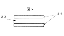
(3)接着剤層の作成:接着剤組成物を溶剤に溶解した塗料を、離型性を有するポリエステルフィルム上に塗布、乾燥する。接着剤層の膜厚は10〜100μmとなるように塗布することが好ましい。乾燥条件は、100〜200℃、1〜5分である。溶剤は特に限定されないが、トルエン、キシレン、クロルベンゼン等の芳香族系、メチルエチルケトン、メチルエチルイソブチルケトン等のケトン系、ジメチルホルムアミド、ジメチルアセトアミド、Nメチルピロドリン等の非プロトン系極性溶剤単独あるいは混合物が好適である。塗工、乾燥した接着剤層上にさらに剥離力の弱い離型性を有するポリエステルあるいはポリオレフィン系の保護フィルムをラミネートして接着剤シートを得る。さらに接着剤厚みを増す場合は、該接着剤シートを複数回積層すればよく、場合によってはラミネート後に、例えば40〜100℃で1〜200時間程度エージングして硬化度を調整してもよい。図5に本発明の半導体装置用接着剤シートの構成を例示する。
【0038】
(4)半導体集積回路接続用基板の部品(接着剤付き配線基板)の作成:上記(1)の配線基板層に、上記(3)で作成した接着剤シートの片面の保護フィルムを剥がした後にラミネートする。ラミネート面は導体パターンがある面、またはない面のいずれでもよい。ラミネート温度20〜200℃、圧力0.1〜3MPaが好適である。最後に半導体装置の形状によって、適宜打ち抜き、切断加工が施される。図2に本発明の部品を例示する。
【0039】
(5)半導体集積回路接続用基板の部品(接着剤付きスティフナー)の作成:上記(2)金属板に、上記(3)で作成した接着剤シートの片側の保護フィルムを剥がした後にラミネートする。ラミネート温度20〜200℃、圧力0.1〜3MPaが好適である。また、(B)に上記(3)の塗料を直接塗布して乾燥させ、保護フィルムをラミネートしてもよい。最後に半導体装置の形状によって、適宜打ち抜き、切断加工が施される。図4に本発明の部品の例を示す。
【0040】
(6)半導体装置の作成:(4)の半導体集積回路接続用基板のインナーリード部を、ICの金バンプに熱圧着(インナーリードボンディング)し、ICを搭載する。次いで、封止樹脂による樹脂封止工程を経て半導体装置を作成する。得られた半導体装置を、他の部品を搭載したプリント回路基板等と半田ボールを介して接続し、電子機器への実装をする。また、あらかじめICを上記(1)の配線基板に接続し、樹脂封止を行った、いわゆるTCP型半導体装置を用いることもできる。図1に本発明の半導体装置の一態様の断面図を示す。
【0041】
【実施例】
以下に実施例を挙げて本発明を詳細に説明するが、本発明はこれらの実施例によって何ら限定されるものではない。なお特性評価は次のように行なった。
評価方法
(1)未硬化状態粘着力:接着剤組成物からなる厚さ100μmの接着剤層付きの、厚さ0.1mmの純銅板を、ポリイミドフィルム(宇部興産(株)製“ユーピレックス”75S)に、130℃、0.1MPaの条件でラミネートした。得られたサンプルのポリイミドフィルムを幅2mmになるように切断し、90°方向に50mm/minの速度で剥離し、その際の剥離力を測定した。また、接着剤シートを23℃100時間保存後、同様に剥離力を測定した。
【0042】
(2)導体パターン埋め込み性およびキュア発泡:接着剤組成物からなる厚さ100μmの接着剤層付きの、厚さ0.1mmの純銅板を、(1)の評価用パターンテープの導体パターン面に、130℃、0.1MPaの条件でラミネートした後、エアオーブン中で150℃、2時間加熱キュア処理を行なった。これを、塩化第二鉄を主成分とするエッチング液中に浸漬し、前記純銅板を溶解した。最後に露出した接着剤層を顕微鏡観察してキュア時の発泡および導体パターンの埋め込み性を評価した。
【0043】
(3)硬化後剥離力:(1)と同様に接着剤層付き純銅板をポリイミドフィルムにラミネートした後、エアオーブン中で150℃、2時間加熱キュア処理を行なった。得られたサンプルのポリイミドフィルムを幅2mmになるように切断し、90°方向に50mm/minの速度で剥離し、その際の剥離力を測定した。また、(1)と同様に保存後の剥離力を測定した。
【0044】
(4)流動性:接着剤組成物からなる厚さ100μmの未硬化状態の単膜を幅5mm、長さ30mmにしたものをサンプルとし、長さ方向に50mm/minの速度で引っ張り試験機による弾性率を測定した。また、保存後の引っ張り弾性率を測定した。弾性率は粘度と正相関の関係にあり、弾性率の変化が小さいと、接着剤組成物の架橋反応の進行が生起しておらず、流動性を保持していると考えられる。
【0045】
(5)半田耐熱性:上記(3)の方法で作成した30mm角のサンプルを、85℃、85%RHの雰囲気下で48時間調湿した後、すみやかに半田浴上に60秒間浮かべ、膨れおよび剥がれのない最高温度を測定した。また、保存後の半田耐熱性を測定した。
【0046】
(6)熱サイクル試験:上記(3)の方法で作成した30mm角のサンプルを、熱サイクル試験器(タバイエスペック(株)製、PL−3型)中で、−20℃〜100℃、最低および最高温度で各1時間保持の条件で600サイクル処理し、剥がれの発生を評価した。
【0047】
実施例1
最初にブロック化したNBRを作成した。NBR−C(日本合成ゴム(株)製、PNR−1H 数平均分子量70000)100重量部に対し、イソブチルビニルエーテル40重量部、酸触媒(2−エチルヘキシルホスフェート)0.2重量部加えたものを固形分濃度20%になるようメチルイソブチルケトンに溶かし、45℃で15時間攪拌した。カルボキシル基のブロック化率は水酸化ナトリウム溶液による中和滴定により行なった。
【0048】
上記の得られたブロック化NBRとブロック化していないNBR(上記のPNR−1H)を混合することで任意のカルボキシル基のブロック化率を設定した。実施例1ではブロック化NBR50重量部、非ブロック化NBR50重量部を用いた。エポキシ樹脂(油化シェル(株)製、”エピコート”834、エポキシ当量250、”エピコート”1001、エポキシ当量475)、無機粒子(水酸化アルミニウム、平均粒径1μm、最大粒径5μm)、硬化剤(4、4’−ジアミノジフェニルスルホン)を表1の組成比になるように加え、30℃で攪拌、混合して接着剤溶液を作成した。この接着剤溶液をバーコータで、シリコーン離型剤付きの厚さ25μのポリエチレンテレフタレートフィルム(藤森工業(株)製“フィルムバイナ”NSC)に約50μの乾燥厚さとなるように塗布し,170℃で5分間乾燥した。一方、剥離力の低いシリコーン離型剤付きの厚さ25μのポリエチレンテレフタレートフィルム(藤森工業(株)製“フィルムバイナ”GT)を用いた以外は上記と同一の方法で約50μの乾燥厚さとなるように接着剤層を作成した。剥離力は、NSC(F1)>GT(F2)であった。次いで、これらを接着剤面どうしを合せて2枚積層し、接着剤厚み100μの本発明の半導体装置用接着シートを作成した。図5に構成を示す。この接着剤シートを厚さ0.1mmの純銅板に100℃、0.1MPaの条件でラミネートし、接着剤層付き純銅板を得た。特性を表2に示す。
【0049】
実施例2
ブチルアクリレート65重量部、エチルアクリレート20重量部、アクリロニトリル15重量部、およびメタアクリル酸2重量部からなる成分を乳化重合し、数平均分子量700000のアクリル樹脂を得た。得られたアクリル樹脂を実施例1と同様にビニルエーテルによるブロック化を行ない、表1の組成比になるよう各成分を加え、30℃で攪拌、混合して接着剤溶液を作成した。この接着剤溶液をバーコータを用い、実施例1と同様の方法で接着剤層付き純銅板を得た。特性を表2に示す。
【0050】
実施例3
ブチルアクリレート65重量部、エチルアクリレート20重量部、アクリロニトリル15重量部、およびメタアクリル酸2重量部からなる成分を溶液重合し、数平均分子量10000のアクリル樹脂を得た。得られたアクリル樹脂を実施例1と同様にビニルエーテルによるブロック化を行ない、表1の組成比になるよう各成分を加え、30℃で攪拌、混合して接着剤溶液を作成した。この接着剤溶液をバーコータを用い、実施例1と同様の方法で接着剤層付き純銅板を得た。特性を表2に示す。
【0051】
実施例4
フェノール樹脂(三菱化学(株)製、RESIN−X)を用いて表1の組成比になるように加え、30℃で攪拌、混合して接着剤溶液を作成した。この接着剤溶液をバーコータを用い、実施例1と同様の方法で接着剤層付き純銅板を得た。特性を表2に示す。
【0052】
実施例5
NBR−C(日本合成ゴム(株)製、PNR−1H)100重量部に対し、ジヒドロピラン35重量部、酸触媒(スルホン酸メチル)0.3重量部を加えたものを固形分濃度20%になるようメチルイソブチルケトンに溶かし、60℃で15時間攪拌した。カルボキシル基のブロック化率は水酸化ナトリウム溶液による中和滴定により行なった。
【0053】
上記の得られたブロック化NBRとブロック化していないNBR(上記のPNR−1H)を混合し、カルボキシル基のブロック化率が80%となるようにしたものと他成分を表1の組成比になるように加え、30℃で攪拌、混合して接着剤溶液を作成した。この接着剤溶液をバーコータを用い、実施例1と同様の方法で接着剤層付き純銅板を得た。特性を表2に示す。
【0054】
実施例6
水酸化アルミニウムを添加しなかった他は実施例1と同様の組成比(表1参照)になるように各化合物を加え、30℃で攪拌、混合して接着剤溶液を作成した。この接着剤溶液をバーコータを用い、実施例1と同様の方法で接着剤層付き純銅板を得た。特性を表2に示す。
【0055】
比較例1
各成分物を表1の組成比になるように加え、30℃で攪拌、混合して接着剤溶液を作成した。この接着剤溶液をバーコータを用い、実施例1と同様の方法で接着剤層付き純銅板を得た。特性を表2に示す。カルボキシル基がブロック化されていないNBRを用いたことから、保存後の接着力が実施例1〜5に比べ劣り、また、保存後の弾性率増加による埋め込み不良が生じた。
【0056】
比較例2
ブチルアクリレート65重量部、エチルアクリレート20重量部、アクリロニトリル15重量部、およびメタアクリル酸2重量部からなる成分を溶液重合し、数平均分子量4000のアクリル樹脂を得た。得られたアクリル樹脂を実施例1と同様にビニルエーテルによるブロック化を行ない、表1の組成比になるよう各成分を加え、30℃で攪拌、混合して接着剤溶液を作成した。この接着剤溶液をバーコータを用い、実施例1と同様の方法で接着剤層付き純銅板を得た。特性を表2に示す。アクリル樹脂の分子量が小さすぎることから、接着剤シートの粘着力が強くなり過ぎるため、貼り合わせ加工に支障をきたした。また、弾性率が低く流動性が高すぎるため、貼り合わせ時、接着剤がはみだす不良が生じた。
【0057】
比較例3
ブチルアクリレート65重量部、エチルアクリレート20重量部、アクリロニトリル15重量部、およびメタアクリル酸2重量部からなる成分を乳化重合し、数平均分子量1200000のアクリル樹脂を得た。得られたアクリル樹脂を実施例1と同様にビニルエーテルによるブロック化を行ない、表1の組成比になるよう各成分を加え、30℃で攪拌、混合して接着剤溶液を作成した。この接着剤溶液をバーコータを用い、実施例1と同様の方法で接着剤層付き純銅板を得た。特性を表2に示す。アクリル樹脂の分子量が大きさすぎることから、接着剤シートの粘着力が低くなっており、そのためICパッケージの製造工程で位置ずれによる不良が発生した。また、弾性率が高く流動性が低くすぎるため、配線基板層への埋め込み不良が起こっていた。
【0058】
【表1】
【表2】
表1、表2の実施例、比較例から本発明により得られる半導体集積回路接続用基板の部品は、優れた接着力、耐熱性および加工性をもち、長期保存後も優れた特性を保持していた。
【0061】
【発明の効果】
本発明はこのような問題点を解決し、優れた接着力および耐熱性を長期間保存後も維持したまま、半導体集積回路接続用基板作成時の貼り合わせ加工性に優れた新規な半導体装置用接着剤シートおよびそれを用いた部品ならびに半導体装置を工業的に提供するものである。本発明の接着剤シートによって高密度実装用の半導体集積回路接続用基板ならびに半導体装置の信頼性および易加工性を向上させることができた。
【図面の簡単な説明】
【図1】本発明の半導体装置用接着剤組成物および半導体装置用接着剤シートを用いたBGA型半導体装置の一態様の概略断面図。
【図2】本発明の半導体装置用接着剤組成物を用いた半導体集積回路接続前の半導体集積回路接続用基板の一態様の概略断面図。
【図3】半導体集積回路接続用基板を構成するパターンテープ(TABテープ)の一態様の概略斜視図。
【図4】本発明の半導体集積回路接続用基板の部品(接着剤付きヒートスプレッター)の一態様の概略断面図。
【図5】本発明の半導体装置用接着剤シートの一態様の概略断面図。
【符号の説明】
1 半導体集積回路
2 金バンプ
3,11,17 可撓性を有する絶縁性フィルム
4,12,18 配線基板層を構成する接着剤層
5,13,21 半導体集積回路接続用の導体
6,14,23 本発明の接着剤組成物より構成される接着剤層
7,15 導体パターンが形成されていない層
8,16 ソルダーレジスト
9 半田ボール
10 封止樹脂
19 スプロケット孔
20 デバイス孔
22 半田ボール接続用の導体部
24 本発明の接着剤シートを構成する保護フィルム層[0001]
BACKGROUND OF THE INVENTION
The present invention relates to an adhesive sheet for a semiconductor device used when a semiconductor integrated circuit (IC) is mounted and packaged, a component using the same, and a semiconductor device. More specifically, a wiring substrate layer comprising an insulating layer and a conductor pattern constituting a substrate for connecting a semiconductor integrated circuit used in a ball grid array (BGA) or land grid array (LGA) surface mount package, and a metal reinforcing plate, for example The present invention relates to an adhesive sheet for a semiconductor device that is used to bond (stiffeners, heat spreaders) and has a function of relaxing thermal stress generated between the respective layers due to a temperature difference, a component using the same, and a semiconductor device.
[0002]
[Prior art]
Conventionally, package forms such as a dual inline package (DIP), a small outline package (SOP), and a quad flat package (QFP) have been used as semiconductor integrated circuit (IC) packages. However, with the increase in the number of pins of ICs and the miniaturization of packages, the QFP that can increase the number of pins is approaching the limit. This is due to the fact that the flatness of the leads is difficult to maintain, and the solder printing accuracy on the printed circuit board is difficult to obtain, especially when mounted on a printed circuit board. Therefore, in recent years, the BGA method, LGA method, PGA method, etc. have been put into practical use as means for increasing the number of pins and reducing the size. Among them, the BGA method has been attracting attention because of the possibility of cost reduction, weight reduction and thinning by using plastic materials.
[0003]
FIG. 1 shows an example of the BGA method. The BGA method is characterized by having
[0004]
On the other hand, the BGA method has the following problems. (A) Keep the solder ball surface flat, (b) improve heat dissipation, (c) relieve thermal stress on the solder ball during temperature cycling and reflow, (d) higher because of the high number of reflows Requires reflow resistance. As a method for improving these, a method of laminating a material such as a metal plate for the purpose of reinforcement, heat dissipation, and electromagnetic shielding on a semiconductor integrated circuit connection substrate is generally used. This is particularly important when a TAB tape or a flexible printed board is used for the wiring board layer composed of the
[0005]
From the above points, the properties required for the
[0006]
In particular, in the processing step (c), since a layer on which no conductor pattern is formed usually emphasizes flatness, a relatively thick metal plate is often used, and a TAB tape or a flexible printed board is used. It is difficult to continuously perform the bonding process with the wiring board layer supplied as a continuous tape. Therefore, it is more general that these are punched into a sheet having a size close to that of the final semiconductor device (BGA package) and bonded to a continuous tape-shaped wiring substrate layer. Therefore, an appropriate adhesive force is required so as not to cause a positional shift in the process from the pasting to the heating cure.
[0007]
From such a viewpoint, conventionally, a thermoplastic resin or a silicone elastomer (Japanese Patent Publication No. 6-50448) has been proposed as an adhesive layer. Further, those using a compound having a blocked carboxyl group include cyclic vinyl ethers such as aliphatic vinyl ethers and dihydropyran, and those using dimethylformamide-dimethylacetal (Japanese Patent Laid-Open No. 4-80242).
[0008]
[Problems to be solved by the invention]
In the conventional adhesive sheet, sufficient characteristics are not necessarily obtained in the adhesive force in the process from bonding to heating curing. For example, an adhesive sheet made of a thermoplastic resin has the advantage that heat curing is not required if the initial adhesive force can be secured, while it has a high softening point to withstand solder reflow, so that the resin in the bonding process There is a problem of requiring high heating and pressurization exceeding the softening point. On the other hand, in an adhesive sheet made of a thermosetting resin, misalignment in a process from pasting to heating curing is prevented by an adhesive force resulting from a low-viscosity uncured resin component. However, since the curing reaction proceeds gradually even during storage of the adhesive sheet, the adhesive force of the adhesive sheet decreases due to an increase in viscosity. Therefore, a defect due to misalignment may occur even though the adhesive strength after heat curing is sufficiently developed. In addition, due to the progress of the curing reaction during storage, the fluidity at the time of bonding of the adhesive sheet is lowered, resulting in insufficient embedding of the wiring board layer into the unevenness. If even a small amount of air bubbles enter the bonded surface due to this insufficient embedding, foaming may occur during solder reflow.
[0009]
Even when a compound having a blocked carboxyl group as disclosed in JP-A-4-80242 is used, it is necessary to consider suitable physical property values in order to obtain good thermal cycleability.
[0010]
The present invention solves such problems and is used for a novel semiconductor device having excellent bonding workability when creating a substrate for connecting a semiconductor integrated circuit while maintaining excellent adhesive strength and heat resistance after long-term storage. An object of the present invention is to provide an adhesive sheet, a component using the adhesive sheet, and a semiconductor device.
[0011]
[Means for Solving the Invention]
That is, the present invention has a blocked carboxyl group represented by the general formula (1). Number Thermoplastic resin having an average molecular weight of 5,000 to 1,000,000 Contains 100 parts by weight and 5-400 parts by weight of epoxy resin An adhesive sheet for a semiconductor device having an adhesive layer, a component using the same, and a semiconductor device.
[0012]
[Chemical formula 2]
(R above 1 , R 2 , R Three Each represents hydrogen or an organic group having 1 to 18 carbon atoms, and each may be the same or different; Four Represents an organic group having 1 to 18 carbon atoms. R Three And R Four May be bonded to each other to form a heterocyclic ring. )
[0014]
DETAILED DESCRIPTION OF THE INVENTION
Hereinafter, the configuration of the present invention will be described in detail.
The adhesive sheet for a semiconductor in the present invention is an interlayer adhesive for a stiffener, a heat spreader, a semiconductor element or a wiring board (interposer), and the shape and material of these adherends are not particularly limited.
[0015]
The adhesive sheet for semiconductor of the present invention contains a compound having a blocked carboxyl group represented by the general formula (1). The carboxyl group is considered to be effective for developing an adhesive force to metal, plastic, film and the like. Furthermore, heat resistance can be improved by reacting a carboxyl group and an epoxy group. If the adhesive sheet of the present invention does not contain a compound having a blocked carboxyl group, it causes a decrease in the adhesive strength of the adhesive sheet after long-term storage, and a defect due to misalignment occurs in the IC package manufacturing process. Further, insufficient embedding in the wiring board layer occurs due to a decrease in fluidity.
[0016]
In particular, when X in the general formula (1) is carboxyl group blocking with vinyl ether, the blocking reaction can be easily carried out at a low temperature, and the carboxyl group regeneration reaction during the thermosetting reaction occurs at 200 ° C. or lower, so that general industrial conditions Can be used. In addition, there are advantages such as no harmful by-products. The blocking ratio of the carboxyl group is preferably 5% or more, more preferably 15% or more, and further preferably 50% or more. If it is less than 5%, an effect on the storage life of the adhesive sheet is not observed.
[0017]
R in the general formula (1) 1 ~ R Three Each represents a hydrogen atom or an organic group having 1 to 18 carbon atoms, and each may be the same or different. Specific examples include alkyl groups such as a methyl group, an ethyl group, a propyl group, a butyl group, an isobutyl group, and a cyclohexyl group. Also R Four Represents an organic group having 1 to 18 carbon atoms, R Three And R Four May be bonded to each other to form a heterocyclic ring. Examples of the heterocyclic ring include a tetrahydrofuran ring and a tetrahydropyran ring.
[0018]
The compound having a blocked carboxyl group has a number average molecular weight of preferably from 5,000 to 1,000,000, more preferably from 10,000 to 500,000. If the number average molecular weight is less than 5000, the adhesive strength of the adhesive sheet becomes too strong, which hinders the bonding process. Further, the fluidity becomes too high, and there is a possibility that the adhesive protrudes during bonding. When the number average molecular weight is larger than 1,000,000, the viscosity of the coating composition of the adhesive composition becomes high, which causes a problem when the adhesive sheet is manufactured. Further, the adhesive strength of the adhesive sheet is reduced, and a defect due to misalignment occurs in the manufacturing process of the IC package. In addition, the fluidity becomes too low, resulting in insufficient embedding in the wiring board layer.
[0019]
Although the compound which has a carboxyl group is not specifically limited, High molecular compounds, such as a thermoplastic resin, are suitable from balance, such as moderate heat fluidity in an uncured state, and elasticity after hardening. Examples thereof include acrylonitrile-butadiene copolymer (NBR-C), styrene-butadiene-ethylene resin (SEBS-C), styrene-butadiene resin (SBS-C), polyester, polyamide, and the like. Among these, copolymers having butadiene as an essential copolymer component are particularly preferred from the viewpoint of adhesiveness, flexibility, and thermal stress relaxation effect, and various types can be used. In particular, NBR-C, SEBS-C, and SBS-C are preferable from the viewpoints of adhesion to metal, chemical resistance, and the like.
[0020]
Moreover, it is preferable to contain the self-crosslinking type compound which has 1 or more of the reactive functional groups which can form a chemical bond with a carboxyl group in 1 molecule. Specific examples of the reactive functional group include an epoxy group, a hydroxyl group, an amino group, an imino group, an isocyanate group, an alkoxysilane group, a silanol group, a cyclocarbonate group, an oxazoline group, and an acetal group. These functional groups are preferable because the bond with the compound having a carboxyl group becomes strong and the heat resistance is improved. Moreover, as a compound which has these functional groups, well-known things, such as an epoxy resin, a phenol resin, a melamine resin, a xylene resin, a furan resin, a cyanate ester resin, are illustrated.
[0021]
Especially, an epoxy resin is excellent in insulation and is suitable from the favorable reactivity with above-mentioned NBR-C, SEBS-C, SBS-C, etc. Examples of epoxy resins include bisphenol F, bisphenol A, bisphenol S, resorcinol, diglycidyl ethers such as dihydroxynaphthalene, dicyclopentadiene diphenol, epoxidized phenol novolac, epoxidized cresol novolac, epoxidized trisphenylol methane, epoxy And cycloaliphatic epoxy such as epoxidized tetraphenylolethane, epoxidized metaxylenediamine, and cyclohexaneepoxide. Furthermore, it is effective to use a halogenated epoxy resin, particularly a brominated epoxy resin, for imparting flame retardancy. At this time, although it is possible to impart flame retardancy with a brominated epoxy resin alone, it is more effective to use a mixed system with a non-brominated epoxy resin because the heat resistance of the adhesive is greatly reduced. Examples of brominated epoxy resins include copolymerized epoxy resins of tetrabromobisphenol A and bisphenol A, or brominated phenol novolac type epoxy resins such as “BREN” -S (manufactured by Nippon Kayaku Co., Ltd.). . These brominated epoxy resins may be used in combination of two or more in consideration of bromine content and epoxy equivalent.
[0022]
The addition amount of the epoxy resin is 5 to 400 parts by weight, preferably 50 to 200 parts by weight with respect to 100 parts by weight of the thermoplastic resin having a blocked carboxyl group. If the amount of the epoxy resin added is less than 5 parts by weight, the elastic modulus will decrease significantly at high temperatures, and the semiconductor integrated circuit connection substrate will be deformed during use of the device mounted with the semiconductor device, and handling work in the processing process It is not preferable because it lacks properties. If the amount added exceeds 400 parts by weight, the elastic modulus is high, the coefficient of linear expansion is small, and the effect of mitigating thermal stress is small.
[0023]
Addition of a curing agent such as an epoxy resin and a curing accelerator to the adhesive layer of the present invention is not limited at all. For example, 3,3′5,5′-tetramethyl-4,4′-diaminodiphenylmethane, 3,3′5,5′-tetraethyl-4,4′-diaminodiphenylmethane, 3,3′-dimethyl-5, 5'-diethyl-4,4'-diaminodiphenylmethane, 3,3'-dichloro-4,4'-diaminodiphenylmethane, 2,2'3,3'-tetrachloro-4,4'-diaminodiphenylmethane, 4, 4'-diaminodiphenyl sulfide, 3,3'-diaminobenzophenone, 3,3'-diaminodiphenyl sulfone, 4,4'-diaminodiphenyl sulfone, 3,4'-diaminodiphenyl sulfone, 4,4'-diaminobenzophenone, Aromatic polyamines such as 3,4,4'-triaminodiphenylsulfone, boron trifluoride triethylamine complexes and the like Known amine complexes, imidazole derivatives such as 2-alkyl-4-methylimidazole and 2-phenyl-4-alkylimidazole, organic acids such as phthalic anhydride and trimellitic anhydride, dicyandiamide, and triphenylphosphine Can be used. You may use these individually or in mixture of 2 or more types. The addition amount is preferably 0.1 to 50 parts by weight with respect to 100 parts by weight of the adhesive composition.
[0024]
In addition to the above components, addition of organic and inorganic components such as antioxidants and ion scavengers is not limited as long as the properties of the adhesive are not impaired. Fine inorganic components include metal hydroxides such as aluminum hydroxide, magnesium hydroxide, calcium aluminate hydrate, silica, alumina, zirconium oxide, zinc oxide, antimony trioxide, antimony pentoxide, magnesium oxide, Examples include metal oxides such as titanium oxide, iron oxide, cobalt oxide, chromium oxide, and talc, inorganic salts such as calcium carbonate, metal fine particles such as aluminum, gold, silver, nickel, and iron, or carbon black and glass. Examples of the organic component include crosslinked polymers such as styrene, NBR rubber, acrylic rubber, polyamide, polyimide, and silicone. You may use these individually or in mixture of 2 or more types. In view of dispersion stability, the average particle size of the fine particle component is preferably 0.2 to 5 μm. Moreover, 2-50 weight part of the whole adhesive composition is suitable for a compounding quantity.
[0025]
The component for a semiconductor device (hereinafter referred to as a component) of the present invention is a material in an intermediate processing stage used for producing a semiconductor integrated circuit connection substrate and a semiconductor device. The component has a structure in which at least one wiring board layer composed of an insulating layer and a conductor pattern and / or a layer in which no conductor pattern is formed and an adhesive layer having a protective layer are provided. For example, a flexible printed circuit board or TAB tape is used as a wiring board layer composed of an insulator layer and a conductor pattern, and a B-stage adhesive layer having a polyester protective film (protective layer) treated with silicone on one or both sides is laminated. For example, copper, stainless steel, 42 alloy, or other metal plate is used as a layer on which a wiring board with an agent or a conductor pattern is not formed, and a B-stage adhesive layer having a protective film is laminated on one or both sides in the same manner as described above. The metal plate with an adhesive (such as a stiffener with an adhesive) corresponds to the component of the present invention. Even when each of the wiring board layer composed of the insulator layer and the conductor pattern and the layer where the conductor pattern is not formed are one or more layers, the B-stage adhesive layer having the protective film (protective layer) is laminated on the outermost layer. A so-called adhesive-attached semiconductor integrated circuit connecting substrate is also included in the components of the present invention.
[0026]
The protective layer here is usually composed of a protective film, and is not particularly limited as long as it can be peeled without damaging its form and function before adhering the adhesive layer. Specific examples thereof include polyester, polyolefin, polyphenylene sulfide, Polyvinyl chloride, polytetrafluoroethylene, polyvinyl fluoride, polyvinyl butyral, polyvinyl acetate, polyvinyl alcohol, polycarbonate, polyamide, polyimide, polymethyl methacrylate and other plastic films, and release agents such as silicone or fluorine compounds. Examples thereof include films subjected to coating treatment, paper laminated with these films, and paper impregnated or coated with a releasable resin. The thickness of the protective film is 20 μm or more, preferably 25 μm or more, and more preferably 35 μm or more from the viewpoint of heat resistance.
[0027]
The peel strength of the protective layer with respect to the adhesive layer is preferably 1 to 200 N / m, more preferably 3 to 100 N / m. If it is lower than 1 N / m, the protective film tends to fall off, and if it exceeds 200 N / m, peeling becomes difficult.
[0028]
The semiconductor device referred to in the present invention means a device using the substrate for connecting a semiconductor integrated circuit of the present invention. For example, the shape and structure are not particularly limited as long as it is a BGA type or LGA type package. The semiconductor integrated circuit connecting substrate and IC can be connected by any of TAB gang bonding and single point bonding, wire bonding used for lead frames, resin sealing in flip chip mounting, anisotropic conductive film connection, etc. Good. A package called CSP is also included in the semiconductor device of the present invention.
[0029]
The wiring board layer is a layer having a conductor pattern for connecting the electrode pad of the semiconductor element and the outside of the package (printed board or the like), and the conductor pattern is formed on one side or both sides of the insulator layer. .
[0030]
The insulator layer here is made of a composite material such as polyimide, polyester, polyphenylene sulfide, polyethersulfone, polyetheretherketone, aramid, polycarbonate, polyarylate, or a plastic or epoxy resin-impregnated glass cloth. A ceramic substrate such as an insulating film having a flexibility of 125 μm, alumina, zirconia, soda glass, and quartz glass is suitable, and a plurality of layers selected from these may be laminated and used. If necessary, the insulator layer can be subjected to surface treatment such as hydrolysis, corona discharge, low temperature plasma, physical roughening, and easy adhesion coating treatment.
[0031]
The formation of the conductor pattern is generally performed by either the subtractive method or the additive method, but any of them may be used in the present invention.
[0032]
In the subtractive method, a metal plate such as copper foil is bonded to the insulator layer with an insulating adhesive, or a precursor of the insulator layer is laminated on the metal plate, and the insulator layer is formed by heat treatment or the like. A pattern is formed by etching the material prepared in (1) by chemical treatment. Specific examples of the material include a rigid or a copper paste material for a flexible printed circuit board and a TAB tape. Among them, a copper paste material for a flexible printed circuit board or a TAB tape, in which at least one polyimide film is an insulator layer and a copper foil is a conductor pattern, is preferably used.
[0033]
In the additive method, a conductor pattern is directly formed on the insulator layer by electroless plating, electrolytic plating, sputtering, or the like. In either case, the formed conductor may be plated with a metal having high corrosion resistance to prevent corrosion. Further, via holes may be formed in the wiring board layer as necessary, and conductor patterns formed on both surfaces may be connected by plating.
[0034]
The metal plate reinforces the wiring board and stabilizes its dimensions (referred to as a reinforcing board or stiffener), electromagnetic shielding between the outside and the IC, heat dissipation from the IC (referred to as a heat spreader, heat sink), semiconductor integrated circuit connection board It carries functions such as imparting flame retardancy to the substrate and imparting distinctiveness according to the shape of the substrate for connecting a semiconductor integrated circuit. Therefore, the shape is not limited to the layer shape, and may have a fin structure for heat dissipation, for example. Any material may be used as long as it has the above functions, and the material is not particularly limited. Metals include copper, iron, aluminum, gold, silver, nickel, and titanium, inorganic materials include alumina, zirconia, soda glass, quartz glass, and carbon, and organic materials include polyimide, polyamide, polyester, and vinyl. Polymer materials such as those based on phenol, phenol, and epoxy. Moreover, the composite material by these combination can also be used. Examples thereof include a thin metal plated shape on a polyimide film, a polymer kneaded with carbon to give conductivity, and a metal plate coated with an organic insulating polymer. If necessary, the insulator layer can be subjected to surface treatment such as hydrolysis, corona discharge, low temperature plasma, physical roughening, and easy adhesion coating treatment.
[0035]
Next, an example of the adhesive sheet for a semiconductor device of the present invention, components constituting the same, and a method for manufacturing the semiconductor device will be described.
[0036]
(1) Creation of a wiring board comprising an insulator layer and a conductor pattern: A three-layer TAB tape in which an adhesive layer and a protective layer are laminated on a polyimide film is processed by the following steps (a) to (d). . (A) Drilling of sprockets and device holes, (b) Thermal lamination with copper foil, (c) Pattern formation (resist application, etching, resist removal), (d) Tin or gold plating treatment. The shape of the TAB tape (pattern tape) obtained is illustrated in FIG.
[0037]
(2) Creation of a layer in which no conductor pattern is formed: A metal plate such as a copper plate or a stainless steel plate having a thickness of 0.05 to 0.5 mm is degreased with acetone.
(3) Preparation of adhesive layer: A paint in which the adhesive composition is dissolved in a solvent is applied onto a polyester film having releasability and dried. It is preferable to apply so that the thickness of the adhesive layer is 10 to 100 μm. Drying conditions are 100 to 200 ° C. and 1 to 5 minutes. Solvents are not particularly limited, but aromatic systems such as toluene, xylene and chlorobenzene, ketone systems such as methyl ethyl ketone and methyl ethyl isobutyl ketone, aprotic polar solvents such as dimethylformamide, dimethylacetamide and N-methylpyrodoline alone or as a mixture Is preferred. An adhesive sheet is obtained by laminating a polyester or polyolefin-based protective film having releasability with a weaker peeling force on the coated and dried adhesive layer. When the thickness of the adhesive is further increased, the adhesive sheet may be laminated a plurality of times. In some cases, after the lamination, for example, the degree of curing may be adjusted by aging at 40 to 100 ° C. for about 1 to 200 hours. FIG. 5 illustrates the configuration of the adhesive sheet for a semiconductor device of the present invention.
[0038]
(4) Preparation of semiconductor integrated circuit connection board component (wiring board with adhesive): After peeling off the protective film on one side of the adhesive sheet prepared in (3) above on the wiring board layer in (1) above Laminate. The laminate surface may be a surface with or without a conductor pattern. A laminating temperature of 20 to 200 ° C. and a pressure of 0.1 to 3 MPa are suitable. Finally, depending on the shape of the semiconductor device, it is appropriately punched and cut. FIG. 2 illustrates the component of the present invention.
[0039]
(5) Preparation of semiconductor integrated circuit connection substrate component (stiffener with adhesive): (2) The metal plate is laminated after peeling off the protective film on one side of the adhesive sheet prepared in (3) above. A laminating temperature of 20 to 200 ° C. and a pressure of 0.1 to 3 MPa are suitable. Further, the coating material of (3) may be directly applied to (B) and dried, and a protective film may be laminated. Finally, depending on the shape of the semiconductor device, it is appropriately punched and cut. FIG. 4 shows an example of the component of the present invention.
[0040]
(6) Preparation of semiconductor device: The inner lead portion of the semiconductor integrated circuit connection substrate of (4) is thermocompression bonded (inner lead bonding) to the gold bump of the IC, and the IC is mounted. Next, a semiconductor device is formed through a resin sealing process using a sealing resin. The obtained semiconductor device is connected to a printed circuit board or the like on which other components are mounted via solder balls, and mounted on an electronic device. In addition, a so-called TCP type semiconductor device in which an IC is connected in advance to the wiring substrate of (1) and resin sealing is performed can also be used. FIG. 1 is a cross-sectional view of one embodiment of a semiconductor device of the present invention.
[0041]
【Example】
EXAMPLES The present invention will be described in detail below with reference to examples, but the present invention is not limited to these examples. The characteristic evaluation was performed as follows.
Evaluation methods
(1) Uncured adhesive strength: A 0.1 mm thick pure copper plate with an adhesive layer made of an adhesive composition and having a thickness of 100 μm is applied to a polyimide film (“UPILEX” 75S manufactured by Ube Industries, Ltd.). And 130 ° C. and 0.1 MPa. The obtained polyimide film of the sample was cut so as to have a width of 2 mm, peeled in the 90 ° direction at a speed of 50 mm / min, and the peel force at that time was measured. Further, after the adhesive sheet was stored at 23 ° C. for 100 hours, the peel force was measured in the same manner.
[0042]
(2) Conductor pattern embedding and cure foaming: A 0.1 mm thick pure copper plate with an adhesive layer made of an adhesive composition and having a thickness of 100 μm is applied to the conductor pattern surface of the evaluation pattern tape of (1). After laminating under conditions of 130 ° C. and 0.1 MPa, a heat curing treatment was performed in an air oven at 150 ° C. for 2 hours. This was immersed in an etching solution containing ferric chloride as a main component to dissolve the pure copper plate. Finally, the exposed adhesive layer was observed with a microscope to evaluate foaming during curing and embedding of the conductor pattern.
[0043]
(3) Peeling force after curing: After laminating a pure copper plate with an adhesive layer on a polyimide film in the same manner as in (1), a heat curing treatment was performed at 150 ° C. for 2 hours in an air oven. The obtained polyimide film of the sample was cut so as to have a width of 2 mm, peeled in the 90 ° direction at a speed of 50 mm / min, and the peel force at that time was measured. Further, the peel strength after storage was measured as in (1).
[0044]
(4) Flowability: An uncured single film made of an adhesive composition having a thickness of 100 μm and having a width of 5 mm and a length of 30 mm is used as a sample, and a tensile tester is used at a speed of 50 mm / min in the length direction. The elastic modulus was measured. Further, the tensile modulus after storage was measured. The elastic modulus has a positive correlation with the viscosity. If the change in the elastic modulus is small, it is considered that the cross-linking reaction of the adhesive composition does not occur and the fluidity is maintained.
[0045]
(5) Solder heat resistance: A 30 mm square sample prepared by the method of (3) above was conditioned for 48 hours in an atmosphere of 85 ° C. and 85% RH, and then immediately floated on the solder bath for 60 seconds and swollen. And the maximum temperature without peeling was measured. In addition, the solder heat resistance after storage was measured.
[0046]
(6) Thermal cycle test: A 30 mm square sample prepared by the method of (3) above is -20 ° C to 100 ° C, minimum in a thermal cycle tester (PL-3 type, manufactured by Tabay Espec Co., Ltd.) Then, 600 cycles were performed under the condition of holding for 1 hour at the maximum temperature, and the occurrence of peeling was evaluated.
[0047]
Example 1
First, the blocked NBR was created. Solids obtained by adding 40 parts by weight of isobutyl vinyl ether and 0.2 parts by weight of an acid catalyst (2-ethylhexyl phosphate) to 100 parts by weight of NBR-C (manufactured by Nippon Synthetic Rubber Co., Ltd., PNR-1H number average molecular weight 70000) It was dissolved in methyl isobutyl ketone so as to have a partial concentration of 20% and stirred at 45 ° C. for 15 hours. The blocking rate of the carboxyl group was determined by neutralization titration with a sodium hydroxide solution.
[0048]
The blocking ratio of an arbitrary carboxyl group was set by mixing the above-obtained blocked NBR and non-blocked NBR (the above PNR-1H). In Example 1, 50 parts by weight of blocked NBR and 50 parts by weight of non-blocked NBR were used. Epoxy resin (“Equacoat” 834, Epoxy equivalent 250, “Epicoat” 1001, Epoxy equivalent 475), inorganic particles (aluminum hydroxide,
[0049]
Example 2
A component consisting of 65 parts by weight of butyl acrylate, 20 parts by weight of ethyl acrylate, 15 parts by weight of acrylonitrile and 2 parts by weight of methacrylic acid was emulsion-polymerized to obtain an acrylic resin having a number average molecular weight of 700,000. The obtained acrylic resin was blocked with vinyl ether in the same manner as in Example 1, and each component was added so as to have the composition ratio shown in Table 1, and the mixture was stirred and mixed at 30 ° C. to prepare an adhesive solution. A pure copper plate with an adhesive layer was obtained from this adhesive solution in the same manner as in Example 1 using a bar coater. The characteristics are shown in Table 2.
[0050]
Example 3
A component comprising 65 parts by weight of butyl acrylate, 20 parts by weight of ethyl acrylate, 15 parts by weight of acrylonitrile and 2 parts by weight of methacrylic acid was solution polymerized to obtain an acrylic resin having a number average molecular weight of 10,000. The obtained acrylic resin was blocked with vinyl ether in the same manner as in Example 1, and each component was added so as to have the composition ratio shown in Table 1, and the mixture was stirred and mixed at 30 ° C. to prepare an adhesive solution. A pure copper plate with an adhesive layer was obtained from this adhesive solution in the same manner as in Example 1 using a bar coater. The characteristics are shown in Table 2.
[0051]
Example 4
A phenol resin (Made by Mitsubishi Chemical Co., Ltd., RESIN-X) was added so as to have the composition ratio shown in Table 1, and the mixture was stirred and mixed at 30 ° C. to prepare an adhesive solution. A pure copper plate with an adhesive layer was obtained from this adhesive solution in the same manner as in Example 1 using a bar coater. The characteristics are shown in Table 2.
[0052]
Example 5
NBR-C (manufactured by Nippon Synthetic Rubber Co., Ltd., PNR-1H) with 100 parts by weight of dihydropyran 35 parts by weight and acid catalyst (methyl sulfonate) 0.3 parts by weight,
[0053]
The above-obtained blocked NBR and non-blocked NBR (PNR-1H above) are mixed, so that the carboxyl group blocking rate is 80% and other components in the composition ratio of Table 1. The mixture was stirred and mixed at 30 ° C. to prepare an adhesive solution. A pure copper plate with an adhesive layer was obtained from this adhesive solution in the same manner as in Example 1 using a bar coater. The characteristics are shown in Table 2.
[0054]
Example 6
Each compound was added so that it might become the composition ratio (refer Table 1) similar to Example 1 except not having added aluminum hydroxide, and it stirred and mixed at 30 degreeC, and created the adhesive solution. A pure copper plate with an adhesive layer was obtained from this adhesive solution in the same manner as in Example 1 using a bar coater. The characteristics are shown in Table 2.
[0055]
Comparative Example 1
Each component was added so that it might become the composition ratio of Table 1, and it stirred and mixed at 30 degreeC and created the adhesive agent solution. A pure copper plate with an adhesive layer was obtained from this adhesive solution in the same manner as in Example 1 using a bar coater. The characteristics are shown in Table 2. Since NBR in which the carboxyl group was not blocked was used, the adhesive strength after storage was inferior to that of Examples 1 to 5, and poor embedding due to an increase in elastic modulus after storage occurred.
[0056]
Comparative Example 2
A component comprising 65 parts by weight of butyl acrylate, 20 parts by weight of ethyl acrylate, 15 parts by weight of acrylonitrile, and 2 parts by weight of methacrylic acid was solution polymerized to obtain an acrylic resin having a number average molecular weight of 4000. The obtained acrylic resin was blocked with vinyl ether in the same manner as in Example 1, and each component was added so as to have the composition ratio shown in Table 1, and the mixture was stirred and mixed at 30 ° C. to prepare an adhesive solution. A pure copper plate with an adhesive layer was obtained from this adhesive solution in the same manner as in Example 1 using a bar coater. The characteristics are shown in Table 2. Since the molecular weight of the acrylic resin is too small, the adhesive strength of the adhesive sheet becomes too strong, which hinders the bonding process. Further, since the elastic modulus was low and the fluidity was too high, a defect that the adhesive protruded during bonding was caused.
[0057]
Comparative Example 3
A component consisting of 65 parts by weight of butyl acrylate, 20 parts by weight of ethyl acrylate, 15 parts by weight of acrylonitrile, and 2 parts by weight of methacrylic acid was emulsion-polymerized to obtain an acrylic resin having a number average molecular weight of 1200,000. The obtained acrylic resin was blocked with vinyl ether in the same manner as in Example 1, and each component was added so as to have the composition ratio shown in Table 1, and the mixture was stirred and mixed at 30 ° C. to prepare an adhesive solution. A pure copper plate with an adhesive layer was obtained from this adhesive solution in the same manner as in Example 1 using a bar coater. The characteristics are shown in Table 2. Since the molecular weight of the acrylic resin is too large, the adhesive force of the adhesive sheet is low, and therefore a defect due to misalignment occurs in the IC package manufacturing process. Further, since the elastic modulus is high and the fluidity is too low, poor embedding in the wiring board layer has occurred.
[0058]
[Table 1]
[Table 2]
The parts of the substrate for connecting a semiconductor integrated circuit obtained by the present invention from the examples and comparative examples in Tables 1 and 2 have excellent adhesive strength, heat resistance and workability, and retain excellent characteristics even after long-term storage. It was.
[0061]
【The invention's effect】
The present invention solves such problems and is used for a novel semiconductor device having excellent bonding workability when creating a substrate for connecting a semiconductor integrated circuit while maintaining excellent adhesive strength and heat resistance after long-term storage. An adhesive sheet, parts using the adhesive sheet, and a semiconductor device are provided industrially. With the adhesive sheet of the present invention, it was possible to improve the reliability and ease of processing of a semiconductor integrated circuit connection substrate for high-density mounting and a semiconductor device.
[Brief description of the drawings]
FIG. 1 is a schematic cross-sectional view of one embodiment of a BGA type semiconductor device using the adhesive composition for a semiconductor device and the adhesive sheet for a semiconductor device of the present invention.
FIG. 2 is a schematic cross-sectional view of one embodiment of a substrate for connecting a semiconductor integrated circuit before connecting the semiconductor integrated circuit using the adhesive composition for a semiconductor device of the present invention.
FIG. 3 is a schematic perspective view of one aspect of a pattern tape (TAB tape) constituting a substrate for connecting a semiconductor integrated circuit.
FIG. 4 is a schematic cross-sectional view of one embodiment of a component (heat spreader with adhesive) of a substrate for connecting a semiconductor integrated circuit according to the present invention.
FIG. 5 is a schematic cross-sectional view of one embodiment of the adhesive sheet for a semiconductor device of the present invention.
[Explanation of symbols]
1 Semiconductor integrated circuit
2 Gold bump
3,11,17 Insulating film having flexibility
4, 12, 18 Adhesive layer constituting wiring board layer
5, 13, 21 Conductor for connecting a semiconductor integrated circuit
6,14,23 Adhesive layer composed of the adhesive composition of the present invention
7,15 Layer with no conductor pattern
8,16 Solder resist
9 Solder balls
10 Sealing resin
19 Sprocket hole
20 Device hole
22 Conductor for solder ball connection
24 Protective film layer constituting the adhesive sheet of the present invention
Claims (5)
Priority Applications (1)
| Application Number | Priority Date | Filing Date | Title |
|---|---|---|---|
| JP08107899A JP4359954B2 (en) | 1999-03-25 | 1999-03-25 | Adhesive sheet for semiconductor device, component using the same, and semiconductor device |
Applications Claiming Priority (1)
| Application Number | Priority Date | Filing Date | Title |
|---|---|---|---|
| JP08107899A JP4359954B2 (en) | 1999-03-25 | 1999-03-25 | Adhesive sheet for semiconductor device, component using the same, and semiconductor device |
Publications (3)
| Publication Number | Publication Date |
|---|---|
| JP2000273415A JP2000273415A (en) | 2000-10-03 |
| JP2000273415A5 JP2000273415A5 (en) | 2006-03-30 |
| JP4359954B2 true JP4359954B2 (en) | 2009-11-11 |
Family
ID=13736369
Family Applications (1)
| Application Number | Title | Priority Date | Filing Date |
|---|---|---|---|
| JP08107899A Expired - Fee Related JP4359954B2 (en) | 1999-03-25 | 1999-03-25 | Adhesive sheet for semiconductor device, component using the same, and semiconductor device |
Country Status (1)
| Country | Link |
|---|---|
| JP (1) | JP4359954B2 (en) |
Cited By (1)
| Publication number | Priority date | Publication date | Assignee | Title |
|---|---|---|---|---|
| CN102898966A (en) * | 2011-07-25 | 2013-01-30 | 日东电工株式会社 | Glue sheet and use thereof |
Families Citing this family (3)
| Publication number | Priority date | Publication date | Assignee | Title |
|---|---|---|---|---|
| JP4721309B2 (en) * | 2001-02-14 | 2011-07-13 | 日東電工株式会社 | Thermosetting resin composition and semiconductor device |
| JP2002241469A (en) * | 2001-02-14 | 2002-08-28 | Nitto Denko Corp | Thermosetting resin composition and semiconductor device |
| JP2010006929A (en) * | 2008-06-26 | 2010-01-14 | Shin-Etsu Chemical Co Ltd | Adhesive composition, adhesive sheet, and dicing die attach film |
-
1999
- 1999-03-25 JP JP08107899A patent/JP4359954B2/en not_active Expired - Fee Related
Cited By (1)
| Publication number | Priority date | Publication date | Assignee | Title |
|---|---|---|---|---|
| CN102898966A (en) * | 2011-07-25 | 2013-01-30 | 日东电工株式会社 | Glue sheet and use thereof |
Also Published As
| Publication number | Publication date |
|---|---|
| JP2000273415A (en) | 2000-10-03 |
Similar Documents
| Publication | Publication Date | Title |
|---|---|---|
| KR100417776B1 (en) | Adhesive Sheet for Semiconductor Connecting Substrate, Adhesive-Backed Tape for TAB, Adhesive-Backed Tape for Wire-Bonding Connection, Semiconductor Connecting Substrate, and Semiconductor Device | |
| JP4893046B2 (en) | Adhesive composition for electronic equipment and adhesive sheet for electronic equipment using the same | |
| JPH10178251A (en) | Board for connecting semiconductor integrated circuit, parts constituting it, and semiconductor device | |
| JP3777734B2 (en) | Adhesive composition for semiconductor device and adhesive sheet for semiconductor device using the same | |
| JP2006176764A (en) | Adhesive composition for electronic equipment, adhesive sheet for electronic equipment, and electronic part and electronic equipment using the same | |
| JP4876317B2 (en) | Adhesive composition for semiconductor device, adhesive sheet for semiconductor device using the same, substrate for semiconductor connection, and semiconductor device | |
| JP3956771B2 (en) | Adhesive sheet for semiconductor device, semiconductor connection substrate and semiconductor device | |
| JP4359954B2 (en) | Adhesive sheet for semiconductor device, component using the same, and semiconductor device | |
| JP4742402B2 (en) | Adhesive composition for semiconductor device, adhesive sheet for semiconductor device using the same, and semiconductor device | |
| JP3777732B2 (en) | Adhesive composition for semiconductor device and adhesive sheet for semiconductor device using the same | |
| JPH10178053A (en) | Adhesive composition for semiconductor device and adhesive sheet for semiconductor device using the same | |
| JPH11260839A (en) | Adhesive composition for semiconductor device and adhesive sheet for semiconductor device using the adhesive composition | |
| JPH10178054A (en) | Board for semiconductor integrated circuit connection, component constituting the same, and semiconductor device | |
| JPH10178037A (en) | Semiconductor device adhesive composition and semiconductor device adhesive sheet using the same | |
| JPH10178040A (en) | Board for semiconductor integrated circuit connection, component constituting the same, and semiconductor device | |
| JPH10178066A (en) | Adhesive composition for semiconductor device and adhesive sheet for semiconductor device using the same | |
| JP2005277135A (en) | Adhesive composition for semiconductor, and adhesive sheet for semiconductor using the same, substrate for connecting semiconductor integrated circuit, and semiconductor device | |
| JP2001131499A (en) | Adhesive sheet for semiconductor device, and parts and semiconductor device using same | |
| JP3911776B2 (en) | Adhesive composition for semiconductor device and adhesive sheet for semiconductor device using the same | |
| JP3911777B2 (en) | Adhesive composition for semiconductor device and adhesive sheet for semiconductor device using the same | |
| JPH10178060A (en) | Board for connecting semiconductor integrated circuit and part and semiconductor device constituting the same | |
| JP4092797B2 (en) | Adhesive sheet for semiconductor device, component using the same, and semiconductor device | |
| JPH10178042A (en) | Board for semiconductor integrated circuit connection, component constituting the same, and semiconductor device | |
| JPH10178036A (en) | Board for connecting semiconductor integrated circuit, components therefor and semiconductor device | |
| JP2002373921A (en) | Adhesive material sheet for semiconductor device and component and semiconductor device using the same |
Legal Events
| Date | Code | Title | Description |
|---|---|---|---|
| A521 | Written amendment |
Free format text: JAPANESE INTERMEDIATE CODE: A523 Effective date: 20060210 |
|
| A621 | Written request for application examination |
Free format text: JAPANESE INTERMEDIATE CODE: A621 Effective date: 20060210 |
|
| A131 | Notification of reasons for refusal |
Free format text: JAPANESE INTERMEDIATE CODE: A131 Effective date: 20090519 |
|
| A521 | Written amendment |
Free format text: JAPANESE INTERMEDIATE CODE: A523 Effective date: 20090622 |
|
| TRDD | Decision of grant or rejection written | ||
| A01 | Written decision to grant a patent or to grant a registration (utility model) |
Free format text: JAPANESE INTERMEDIATE CODE: A01 Effective date: 20090721 |
|
| A01 | Written decision to grant a patent or to grant a registration (utility model) |
Free format text: JAPANESE INTERMEDIATE CODE: A01 |
|
| A61 | First payment of annual fees (during grant procedure) |
Free format text: JAPANESE INTERMEDIATE CODE: A61 Effective date: 20090803 |
|
| FPAY | Renewal fee payment (event date is renewal date of database) |
Free format text: PAYMENT UNTIL: 20120821 Year of fee payment: 3 |
|
| FPAY | Renewal fee payment (event date is renewal date of database) |
Free format text: PAYMENT UNTIL: 20120821 Year of fee payment: 3 |
|
| FPAY | Renewal fee payment (event date is renewal date of database) |
Free format text: PAYMENT UNTIL: 20130821 Year of fee payment: 4 |
|
| LAPS | Cancellation because of no payment of annual fees |