JP4349493B2 - Single crystal silicon pulling apparatus, silicon melt contamination prevention method, and silicon melt contamination prevention apparatus - Google Patents
Single crystal silicon pulling apparatus, silicon melt contamination prevention method, and silicon melt contamination prevention apparatus Download PDFInfo
- Publication number
- JP4349493B2 JP4349493B2 JP2005279979A JP2005279979A JP4349493B2 JP 4349493 B2 JP4349493 B2 JP 4349493B2 JP 2005279979 A JP2005279979 A JP 2005279979A JP 2005279979 A JP2005279979 A JP 2005279979A JP 4349493 B2 JP4349493 B2 JP 4349493B2
- Authority
- JP
- Japan
- Prior art keywords
- single crystal
- cylindrical body
- crystal silicon
- heat shield
- pulling
- Prior art date
- Legal status (The legal status is an assumption and is not a legal conclusion. Google has not performed a legal analysis and makes no representation as to the accuracy of the status listed.)
- Active
Links
Images


Classifications
-
- C—CHEMISTRY; METALLURGY
- C30—CRYSTAL GROWTH
- C30B—SINGLE-CRYSTAL GROWTH; UNIDIRECTIONAL SOLIDIFICATION OF EUTECTIC MATERIAL OR UNIDIRECTIONAL DEMIXING OF EUTECTOID MATERIAL; REFINING BY ZONE-MELTING OF MATERIAL; PRODUCTION OF A HOMOGENEOUS POLYCRYSTALLINE MATERIAL WITH DEFINED STRUCTURE; SINGLE CRYSTALS OR HOMOGENEOUS POLYCRYSTALLINE MATERIAL WITH DEFINED STRUCTURE; AFTER-TREATMENT OF SINGLE CRYSTALS OR A HOMOGENEOUS POLYCRYSTALLINE MATERIAL WITH DEFINED STRUCTURE; APPARATUS THEREFOR
- C30B29/00—Single crystals or homogeneous polycrystalline material with defined structure characterised by the material or by their shape
- C30B29/02—Elements
- C30B29/06—Silicon
-
- C—CHEMISTRY; METALLURGY
- C30—CRYSTAL GROWTH
- C30B—SINGLE-CRYSTAL GROWTH; UNIDIRECTIONAL SOLIDIFICATION OF EUTECTIC MATERIAL OR UNIDIRECTIONAL DEMIXING OF EUTECTOID MATERIAL; REFINING BY ZONE-MELTING OF MATERIAL; PRODUCTION OF A HOMOGENEOUS POLYCRYSTALLINE MATERIAL WITH DEFINED STRUCTURE; SINGLE CRYSTALS OR HOMOGENEOUS POLYCRYSTALLINE MATERIAL WITH DEFINED STRUCTURE; AFTER-TREATMENT OF SINGLE CRYSTALS OR A HOMOGENEOUS POLYCRYSTALLINE MATERIAL WITH DEFINED STRUCTURE; APPARATUS THEREFOR
- C30B15/00—Single-crystal growth by pulling from a melt, e.g. Czochralski method
- C30B15/14—Heating of the melt or the crystallised materials
-
- C—CHEMISTRY; METALLURGY
- C30—CRYSTAL GROWTH
- C30B—SINGLE-CRYSTAL GROWTH; UNIDIRECTIONAL SOLIDIFICATION OF EUTECTIC MATERIAL OR UNIDIRECTIONAL DEMIXING OF EUTECTOID MATERIAL; REFINING BY ZONE-MELTING OF MATERIAL; PRODUCTION OF A HOMOGENEOUS POLYCRYSTALLINE MATERIAL WITH DEFINED STRUCTURE; SINGLE CRYSTALS OR HOMOGENEOUS POLYCRYSTALLINE MATERIAL WITH DEFINED STRUCTURE; AFTER-TREATMENT OF SINGLE CRYSTALS OR A HOMOGENEOUS POLYCRYSTALLINE MATERIAL WITH DEFINED STRUCTURE; APPARATUS THEREFOR
- C30B35/00—Apparatus not otherwise provided for, specially adapted for the growth, production or after-treatment of single crystals or of a homogeneous polycrystalline material with defined structure
-
- Y—GENERAL TAGGING OF NEW TECHNOLOGICAL DEVELOPMENTS; GENERAL TAGGING OF CROSS-SECTIONAL TECHNOLOGIES SPANNING OVER SEVERAL SECTIONS OF THE IPC; TECHNICAL SUBJECTS COVERED BY FORMER USPC CROSS-REFERENCE ART COLLECTIONS [XRACs] AND DIGESTS
- Y10—TECHNICAL SUBJECTS COVERED BY FORMER USPC
- Y10T—TECHNICAL SUBJECTS COVERED BY FORMER US CLASSIFICATION
- Y10T117/00—Single-crystal, oriented-crystal, and epitaxy growth processes; non-coating apparatus therefor
- Y10T117/10—Apparatus
- Y10T117/1024—Apparatus for crystallization from liquid or supercritical state
- Y10T117/1032—Seed pulling
- Y10T117/1068—Seed pulling including heating or cooling details [e.g., shield configuration]
-
- Y—GENERAL TAGGING OF NEW TECHNOLOGICAL DEVELOPMENTS; GENERAL TAGGING OF CROSS-SECTIONAL TECHNOLOGIES SPANNING OVER SEVERAL SECTIONS OF THE IPC; TECHNICAL SUBJECTS COVERED BY FORMER USPC CROSS-REFERENCE ART COLLECTIONS [XRACs] AND DIGESTS
- Y10—TECHNICAL SUBJECTS COVERED BY FORMER USPC
- Y10T—TECHNICAL SUBJECTS COVERED BY FORMER US CLASSIFICATION
- Y10T117/00—Single-crystal, oriented-crystal, and epitaxy growth processes; non-coating apparatus therefor
- Y10T117/10—Apparatus
- Y10T117/1024—Apparatus for crystallization from liquid or supercritical state
- Y10T117/1032—Seed pulling
- Y10T117/1072—Seed pulling including details of means providing product movement [e.g., shaft guides, servo means]
-
- Y—GENERAL TAGGING OF NEW TECHNOLOGICAL DEVELOPMENTS; GENERAL TAGGING OF CROSS-SECTIONAL TECHNOLOGIES SPANNING OVER SEVERAL SECTIONS OF THE IPC; TECHNICAL SUBJECTS COVERED BY FORMER USPC CROSS-REFERENCE ART COLLECTIONS [XRACs] AND DIGESTS
- Y10—TECHNICAL SUBJECTS COVERED BY FORMER USPC
- Y10T—TECHNICAL SUBJECTS COVERED BY FORMER US CLASSIFICATION
- Y10T117/00—Single-crystal, oriented-crystal, and epitaxy growth processes; non-coating apparatus therefor
- Y10T117/10—Apparatus
- Y10T117/1024—Apparatus for crystallization from liquid or supercritical state
- Y10T117/1076—Apparatus for crystallization from liquid or supercritical state having means for producing a moving solid-liquid-solid zone
- Y10T117/1088—Apparatus for crystallization from liquid or supercritical state having means for producing a moving solid-liquid-solid zone including heating or cooling details
Description
本発明は、熱遮蔽体からシリコン融液への塵の落下によってシリコン融液が汚染されることを防止する単結晶シリコン引き上げ装置、シリコン融液の汚染防止方法及び装置に関する。 The present invention relates to a single crystal silicon pulling apparatus, a silicon melt contamination prevention method, and an apparatus for preventing the silicon melt from being contaminated by the fall of dust from a heat shield to the silicon melt.
図1は単結晶シリコン引き上げ装置の模式図である。
単結晶引き上げ装置10の炉体1の内部には、炉体1の内壁面の内側に配置され炉体内外の熱伝達を遮断する断熱材2と、多結晶シリコンのようなシリコン材料を保持しこのシリコン原料溶解後のシリコン融液を貯留するルツボ3と、ルツボ3を囲繞するように配置されルツボ3を介してシリコン材料を熱するヒータ4と、単結晶シリコン8の引き上げ経路を囲繞するようにルツボ3の上方に配置される熱遮蔽体5と、が設けられる。
FIG. 1 is a schematic view of a single crystal silicon pulling apparatus.
Inside the furnace body 1 of the single crystal pulling apparatus 10, a heat insulating material 2 disposed inside the inner wall surface of the furnace body 1 to block heat transfer outside the furnace body and a silicon material such as polycrystalline silicon are held. The crucible 3 for storing the silicon melt after dissolution of the silicon raw material, the heater 4 disposed so as to surround the crucible 3 and heating the silicon material via the crucible 3, and the pulling path of the
また単結晶シリコン8の引き上げ経路を囲繞するようにルツボ3の上方に冷却コイル6が設けられる場合もある。冷却コイル6は、冷却水が流れる管路が螺旋状に巻回されて形成されており、全体の形状が筒状である。冷却コイル6は結晶の引き上げ経路が螺旋の内側に位置するようにルツボ3の上方に配置される。冷却コイル6によって単結晶シリコン8の冷却速度が速められると、単結晶シリコン8に含まれる空孔状の欠陥所謂COPのサイズが小さくなるため結晶品質が向上する。また単結晶シリコン8の製造サイクルが早まるため製造効率が向上する。なお単結晶シリコン8の酸素析出物を制御する場合や酸化膜耐圧を改善する場合があり、冷却コイル6の位置とほぼ同位置に冷却コイルではなく筒状の加熱ヒータやパージチューブが設けられることもある。
Further, the
ここで単結晶引き上げ装置10を用いた単結晶シリコン製造処理の手順を簡単に説明する。ルツボ3にシリコン材料を投入しヒータ4を起動する。するとシリコン材料が加熱され溶解しシリコン融液が生成される。生成されたシリコン融液にシリコンの種結晶を浸漬する。この種結晶を引き上げると種結晶の回りには単結晶シリコン8が育成される。単結晶シリコン8の引き上げの際には引き上げ速度や熱遮蔽体5の位置等を調整する。さらに冷却コイル6の管路に冷却水を流して単結晶シリコン8を強制的に冷却する。
Here, the procedure of the single crystal silicon manufacturing process using the single crystal pulling apparatus 10 will be briefly described. Silicon material is put into the crucible 3 and the heater 4 is started. Then, the silicon material is heated and melted to generate a silicon melt. A silicon seed crystal is immersed in the produced silicon melt. When this seed crystal is pulled up,
単結晶シリコン8の育成時には炉体1内の上方からArガスが供給される。図5は一般的な炉体内のガス流を示す図である。図5(a)では単結晶シリコンの育成初期のガス流が示されており、図5(b)では単結晶シリコンの育成初期後のガス流が示されている。
Ar gas is supplied from above in the furnace body 1 when the
図5(a)で示されるように、単結晶シリコン8の育成初期は、炉体1内の上方から供給されるArガスが冷却コイル6の内側を通過してシリコン融液近傍まで下降する。さらにルツボ3とヒータ4の間隙を下降し、炉体1の下部に設けられたガス排出口1aから炉体1の外部に流出する。また炉体1内の上方から供給されるArガスの一部は冷却コイル6の内側を通過した後に、冷却コイル6の下端6aと熱遮蔽体5の間隙を通過して冷却コイル6と熱遮蔽体5の間隙を上昇し、炉体1の上方から供給されるArガスと合流する。
As shown in FIG. 5A, at the initial stage of growth of the
図5(b)で示されるように、単結晶シリコン8の育成初期後は、炉体1内の上方から供給されるArガスの一部が冷却コイル6の内側すなわち冷却コイル6と単結晶シリコン8の間隙を通過してシリコン融液近傍まで下降する。さらにルツボ3とヒータ4の間隙を下降し、炉体1の下部に設けられたガス排出口1aから炉体1の外部に流出する。また炉体1内の上方から供給されるArガスの一部は冷却コイル6と熱遮蔽体5の間隙を下降して冷却コイル6の下端6aと熱遮蔽体5の間隙を通過し、冷却コイル6の内側を通過してきたArガスと合流する。
As shown in FIG. 5B, after the initial growth of the
図5(a)、(b)で示されるように、単結晶シリコン8の育成初期とその後とでは冷却コイル6の下端6aと熱遮蔽体5の間隙を流れるArガスの進行方向が変化する。このとき流速の変化量が大きいと熱遮蔽体5に付着する塵が剥離する場合がある。剥離した塵は熱遮蔽体5に沿って落ち、シリコン融液に落下する。
また炉体1の上部に付着する塵が落下する場合もある。塵は熱遮蔽体5に落下し、熱遮蔽体5に沿って落ち、シリコン融液に落下する。
As shown in FIGS. 5A and 5B, the traveling direction of Ar gas flowing through the gap between the
Moreover, the dust adhering to the upper part of the furnace body 1 may fall. The dust falls on the
シリコン融液に塵が落下するとシリコン融液が汚染されることになる。特にシリコン融液中の塵が育成される結晶に取り込まれると結晶の単結晶化が阻害され、単結晶シリコンの品質が低下するといった問題が生ずる。したがってシリコン融液への塵の落下を防止する必要がある。 When dust falls on the silicon melt, the silicon melt is contaminated. In particular, when dust in the silicon melt is taken into the crystal to be grown, there is a problem that the single crystallization of the crystal is hindered and the quality of the single crystal silicon is lowered. Therefore, it is necessary to prevent the dust from falling into the silicon melt.
本発明はこうした実状に鑑みてなされたものであり、シリコン融液への塵の落下を低減し、単結晶シリコンの品質低下を防止することを解決課題とするものである。 The present invention has been made in view of such a situation, and an object of the present invention is to reduce the fall of dust into the silicon melt and prevent the deterioration of the quality of single crystal silicon.
第1発明は、
単結晶シリコンの引き上げ経路を囲繞する筒状体と、この筒状体を囲繞する上部とこの筒状体よりも下方で単結晶シリコンの引き上げ経路を囲繞する下部とを有し且つ下部の下端の内径が筒状体の内径以下である熱遮蔽体とを炉内に備え、炉内上方から下方へガスを供給しつつ単結晶シリコンを引き上げる単結晶シリコン引き上げ装置において、
単結晶シリコンの側面と筒状体の内壁面とで形成される環状空間のうち、結晶の引き上げ軸と直交する平面に含まれる断面部分の面積をS1とし、且つ筒状体の下端から下方に延在する筒状空間のうち、筒状体と熱遮蔽体との間に位置する部分の側面の面積をS2とした場合に、S2/S1が1.15未満であること
を特徴とする。
The first invention is
A cylindrical body surrounding the single crystal silicon pulling path; an upper part surrounding the cylindrical body; and a lower part surrounding the single crystal silicon pulling path below the cylindrical body; In the single crystal silicon pulling apparatus for pulling up the single crystal silicon while supplying a gas from the upper side to the lower side of the furnace with a heat shield having an inner diameter equal to or smaller than the inner diameter of the cylindrical body ,
Of the annular space formed by the side surface of the single crystal silicon and the inner wall surface of the cylindrical body, the area of the cross-sectional portion included in the plane orthogonal to the crystal pulling axis is S1, and downward from the lower end of the cylindrical body. Of the extending cylindrical space, S2 / S1 is less than 1.15 when the area of the side surface of the portion located between the cylindrical body and the heat shield is S2.
第1発明を説明する。
単結晶シリコン引き上げ装置の炉体内上方からArガスが供給されると、Arガスは単結晶シリコンに沿って下降する。単結晶シリコンの育成初期とその後とでは筒状体の下端と熱遮蔽体の間隙を通過するArガスの進行方向が変化するが、筒状体の下端と熱遮蔽体の間隙を通過するArガスの流速が小さければArガスの進行方向の変化があってもその流速の変化量は小さい。するとArガスの進行方向の変化に起因する熱遮蔽体から塵の剥離することが防止される。よって塵がシリコン融液へ落下することが防止される。
The first invention will be described.
When Ar gas is supplied from above the furnace body of the single crystal silicon pulling apparatus, the Ar gas descends along the single crystal silicon. The progress direction of Ar gas passing through the gap between the lower end of the cylindrical body and the heat shield changes between the initial stage of growth of the single crystal silicon and thereafter, but Ar gas passing through the gap between the lower end of the cylindrical body and the heat shield If the flow rate of the gas is small, the amount of change in the flow rate is small even if there is a change in the direction of travel of Ar gas. Then, it is possible to prevent the dust from being peeled off from the heat shield due to the change in the traveling direction of the Ar gas. Therefore, dust is prevented from falling into the silicon melt.
筒状体の下端と熱遮蔽体の間隙を通過するArガスの流速は、単結晶シリコンの引き上げ経路と筒状体と熱遮蔽体の配置に影響を受ける。したがって単結晶シリコンの引き上げ経路と筒状体と熱遮蔽体の相対的な位置を調整すれば筒状体の下端と熱遮蔽体の間隙を通過するArガスの流速を制御できる。 The flow rate of Ar gas passing through the gap between the lower end of the cylindrical body and the thermal shield is affected by the single crystal silicon pulling path and the arrangement of the cylindrical body and the thermal shield. Therefore, the flow rate of Ar gas passing through the gap between the lower end of the cylindrical body and the heat shield can be controlled by adjusting the single crystal silicon pulling path and the relative positions of the cylindrical body and the heat shield.
具体的には、
単結晶シリコンの側面と筒状体の内壁面とで形成される環状空間のうち、結晶の引き上げ軸と直交する平面に含まれる断面部分の面積をS1とし、且つ筒状体の下端から下方に延在する筒状空間のうち、筒状体と熱遮蔽体との間に位置する部分の側面の面積をS2とした場合に、S2/S1が1.15未満になるように単結晶シリコンの引き上げ経路と筒状体と熱遮蔽体とが配置される。
In particular,
Of the annular space formed by the side surface of the single crystal silicon and the inner wall surface of the cylindrical body, the area of the cross-sectional portion included in the plane orthogonal to the crystal pulling axis is S1, and downward from the lower end of the cylindrical body. In the extending cylindrical space, when the area of the side surface of the portion located between the cylindrical body and the heat shield is S2, the single crystal silicon is made so that S2 / S1 is less than 1.15. A pulling path, a cylindrical body, and a heat shield are arranged.
第2発明は、
単結晶シリコンの引き上げ経路を囲繞する筒状体と、この筒状体を囲繞する上部とこの筒状体よりも下方で単結晶シリコンの引き上げ経路を囲繞する下部とを有し且つ下部の下端の内径が筒状体の内径以下である熱遮蔽体と、を炉内に備えた単結晶シリコン引き上げ装置で、炉内上方から下降するガスによってシリコン融液に塵が落下することを防止するシリコン融液の汚染防止方法において、
単結晶シリコンの側面と筒状体の内壁面とで形成される環状空間のうち、結晶の引き上げ軸と直交する平面に含まれる断面部分の面積をS1とし、且つ筒状体の下端から下方に延在する筒状空間のうち、筒状体と熱遮蔽体との間に位置する部分の側面の面積をS2とした場合に、筒状体の下端と熱遮蔽体との間を通過するガスによってシリコン融液への塵の落下を防止できるようなS2/S1の値を求めておき、
単結晶シリコンの引き上げ時にS2/S1が求めた値になるように単結晶シリコンの引き上げ経路と筒状体と熱遮蔽体の相対的な位置を調整すること
を特徴とする。
The second invention is
A cylindrical body surrounding the single crystal silicon pulling path; an upper part surrounding the cylindrical body; and a lower part surrounding the single crystal silicon pulling path below the cylindrical body; A single crystal silicon pulling device equipped with a heat shield having an inner diameter equal to or smaller than the inner diameter of the cylindrical body, and a silicon melt that prevents dust from falling into the silicon melt by the gas descending from above the furnace. In the method of preventing liquid contamination,
Of the annular space formed by the side surface of the single crystal silicon and the inner wall surface of the cylindrical body, the area of the cross-sectional portion included in the plane orthogonal to the crystal pulling axis is S1, and downward from the lower end of the cylindrical body. Gas that passes between the lower end of the tubular body and the heat shield when the area of the side surface of the portion located between the tubular body and the heat shield in the extending tubular space is S2. The value of S2 / S1 that can prevent the dust from dropping into the silicon melt is obtained,
The single crystal silicon pulling path and the relative positions of the cylindrical body and the heat shield are adjusted so that S2 / S1 becomes the value obtained when pulling the single crystal silicon .
第3発明は、
単結晶シリコンの引き上げ経路を囲繞する筒状体と、この筒状体を囲繞する上部とこの筒状体よりも下方で単結晶シリコンの引き上げ経路を囲繞する下部とを有し且つ下部の下端の内径が筒状体の内径以下である熱遮蔽体と、を炉内に備えた単結晶シリコン引き上げ装置で、炉内上方から下降するガスによってシリコン融液に塵が落下することを防止するシリコン融液の汚染防止方法において、
単結晶シリコンの側面と筒状体の内壁面とで形成される環状空間のうち、結晶の引き上げ軸と直交する平面に含まれる断面部分の面積をS1とし、且つ筒状体の下端から下方に延在する筒状空間のうち、筒状体と熱遮蔽体との間に位置する部分の側面の面積をS2とした場合に、S2/S1を1.15未満とするように単結晶シリコンの引き上げ経路と筒状体と熱遮蔽体の相対的な位置を調整すること
を特徴とする。
The third invention is
A cylindrical body surrounding the single crystal silicon pulling path; an upper part surrounding the cylindrical body; and a lower part surrounding the single crystal silicon pulling path below the cylindrical body; A single crystal silicon pulling device equipped with a heat shield having an inner diameter equal to or smaller than the inner diameter of the cylindrical body, and a silicon melt that prevents dust from falling into the silicon melt by the gas descending from above the furnace. In the method of preventing liquid contamination,
Of the annular space formed by the side surface of the single crystal silicon and the inner wall surface of the cylindrical body, the area of the cross-sectional portion included in the plane orthogonal to the crystal pulling axis is S1, and downward from the lower end of the cylindrical body. In the extending cylindrical space, when the area of the side surface of the portion located between the cylindrical body and the heat shield is S2, the single crystal silicon is made so that S2 / S1 is less than 1.15. It is characterized by adjusting the relative positions of the pulling path, the cylindrical body, and the heat shield.
第2、第3発明は第1発明を方法の発明に置換したものである。The second and third inventions are obtained by replacing the first invention with a method invention.
第4発明は、第1発明の単結晶シリコン引き上げ装置において、4th invention is the single crystal silicon pulling apparatus of 1st invention,
前記筒状体は、 The cylindrical body is
温度調整用の媒体が供給されるパイプが単結晶シリコンの引き上げ経路を略中心にして螺旋状に巻かれてなる温度調整コイルと、 A temperature adjusting coil in which a pipe to which a temperature adjusting medium is supplied is spirally wound around a single crystal silicon pulling path;
前記温度調整コイル下端の全体又は一部に沿って取り付けられて該温度調整コイルと共にコイル体を形成するコイル補完部材と、を有し、 A coil complementary member that is attached along all or part of the lower end of the temperature adjustment coil and forms a coil body together with the temperature adjustment coil, and
前記コイル体下端のいずれの部分と前記熱遮蔽体との間隙が一定であること The gap between any part of the lower end of the coil body and the heat shield is constant.
を特徴とする。 It is characterized by.
螺旋状のパイプからなる温度調整コイルは下端に高低差が生じる。このため温度調整コイルの下端と温度調整コイルの回りを囲繞する熱遮蔽体との間隙が場所によって異なることになる。こうした間隙の不均一を防止するために、温度調整コイルの下端の全体又は一部に高低差を補完するコイル補完部材が取り付けられる。コイル補完部材と温度調整コイルとは一体となりコイル体を形成する。コイル体の下端と熱遮蔽体との間隙はどの部分でも略一定とされる。するとコイル体と熱遮蔽体との間隙でガス流れの不均一化が発生しなくなる。 A temperature adjustment coil formed of a spiral pipe has a height difference at the lower end. For this reason, the gap between the lower end of the temperature adjustment coil and the heat shield surrounding the temperature adjustment coil varies depending on the location. In order to prevent such non-uniformity of the gap, a coil complementing member that complements the height difference is attached to the whole or a part of the lower end of the temperature adjustment coil. The coil complementary member and the temperature adjustment coil are integrated to form a coil body. The gap between the lower end of the coil body and the heat shield is substantially constant at any part. Then, non-uniform gas flow does not occur in the gap between the coil body and the heat shield.
第1〜第3発明によれば、冷却コイルなどの筒状体の下端と熱遮蔽体の間隙を通過するArガスの流速を小さくすることができる。このためガス流の変化に起因する熱遮蔽体表面からの塵の剥離が低減される。よってシリコン融液への塵の落下が低減され、単結晶シリコンの品質低下が防止される。 According to the 1st-3rd invention , the flow velocity of Ar gas which passes the clearance gap between the lower end of cylindrical bodies, such as a cooling coil, and a heat shield can be made small. For this reason, the separation of dust from the surface of the heat shield due to the change of the gas flow is reduced. Therefore, the fall of the dust to a silicon melt is reduced, and the quality fall of a single crystal silicon is prevented.
第4発明によれば、、冷却コイルのような温度調整コイルの下端にコイル補完部材を取り付けてコイル体を形成するため、コイル体の下端と熱遮蔽体との間隙を全ての部分で一定にすることができる。したがってコイル体と熱遮蔽体との間隙でガス流れの不均一化が発生しなくなる。よって炉体内の上部に堆積した微小な塵の落下を誘発することがなくなり、シリコン融液への塵の落下が低減され、単結晶シリコンの品質低下が防止される。 According to the fourth aspect of the present invention , the coil complementary member is attached to the lower end of the temperature adjustment coil such as the cooling coil to form the coil body, so that the gap between the lower end of the coil body and the heat shield is constant in all portions. can do. Therefore, nonuniform gas flow does not occur in the gap between the coil body and the heat shield. Therefore, it does not induce the fall of the minute dust deposited on the upper part of the furnace body, the fall of the dust to the silicon melt is reduced, and the quality deterioration of the single crystal silicon is prevented.
以下、本発明の実施の形態について図面を参照して説明する。
実施例1は冷却コイルの下端と熱遮蔽体の間隙を通過するガス流の制御に関し、実施例2、3は熱遮蔽体の形状に関する。
Hereinafter, embodiments of the present invention will be described with reference to the drawings.
Example 1 relates to control of the gas flow passing through the gap between the lower end of the cooling coil and the heat shield, and Examples 2 and 3 relate to the shape of the heat shield.
本実施形態の装置構成は図1で示される単結晶引き上げ装置10と同じであるが、熱遮蔽体5と冷却コイル6と単結晶シリコン8の引き上げ経路の配置が後述する面積S1、S2を基にして決定されているという点で異なる。
The apparatus configuration of the present embodiment is the same as that of the single crystal pulling apparatus 10 shown in FIG. 1, but the arrangement of the pulling paths of the
熱遮蔽体5と冷却コイル6と単結晶シリコン8の引き上げ経路の相対的な位置は、冷却コイル6の下端6aと熱遮蔽体5の間隙を通過するガスの流速が熱遮蔽体5から塵を剥離させない程度となるように調整される。その位置は、例えば単結晶引き上げ装置10の製造段階で、各構成要素のサイズ・形状に応じて後述する面積比S2/S1を求め決定される。
The relative position of the
また冷却コイル6と熱遮蔽体5のうちの少なくとも一方を昇降動作自在にし、冷却コイル6と熱遮蔽体5の相対的な位置を適宜変化させてもよい。この場合、冷却コイル6と熱遮蔽体5の昇降動作は図示しないコントローラで制御される。なお本実施形態では単結晶シリコン8の引き上げ経路を囲繞する筒状体を冷却コイル6として説明するが、冷却コイル6の代わりに加熱ヒータやパージチューブが設けられる場合にも本発明を適用することが可能である。
Further, at least one of the cooling
図2は本実施形態で用いる面積S1、S2を示す図である。
本実施形態では単結晶シリコン8の引き上げ経路と冷却コイル6と熱遮蔽体5の相対的な位置の調整を面積S1、S2という要素に基づいて行う。
FIG. 2 is a diagram showing the areas S1 and S2 used in the present embodiment.
In the present embodiment, the relative positions of the pulling path of the
単結晶シリコン8の側面と冷却コイル6の内壁面との間には環状空間21が形成される。環状空間21において、軸と直交する平面に含まれる断面部分の断面21aを図2(b)で示す。この断面21aの面積をS1とする。次に冷却コイル6が下方に延在する場合を想定する。このような場合に冷却コイル6の下方には筒状空間22が想定される。この筒状空間22において、冷却コイル6と熱遮蔽体5との間に形成される部分22aを図2(c)で示す。この部分22aの周面の面積をS2とする。
An annular space 21 is formed between the side surface of the
面積S1は引き上げる単結晶シリコン8の径と冷却コイル6の径に応じて決まる。面積S2は熱遮蔽体5の形状と冷却コイル6の径、また熱遮蔽体5及び冷却コイル6の位置に応じて決まる。ここで重要なのは面積S1、S2の値ではなく、その比S2/S1(又はS1/S2)である。
The area S1 is determined according to the diameter of the
表1に面積比S2/S1に関する本発明者の実験データを示す。表1は直径200mmの結晶を引き上げた場合のデータである。 Table 1 shows the inventor's experimental data regarding the area ratio S2 / S1. Table 1 shows data when a crystal having a diameter of 200 mm is pulled up.

シリコン融液中の塵は単結晶シリコンの品質に影響を及ぼす。具体的には塵は結晶の単結晶化を阻害する。シリコン融液中に塵が多いほど生成された結晶の単結晶化率は低くなり、逆に多結晶化率が高くなる。面積比S2/S1を1.15とした場合に生成された結晶は単結晶化率が低く、製品として許容できなかった。面積比S2/S1を1.15未満とした場合(1.01、0.8)に生成された結晶は単結晶化率が高い。本発明者は、面積比S2/S1を1.15とした場合に生成される結晶の単結晶化率が、製品として許容できるか否かの閾値であると考えている。よって面積比S2/S1が1.15未満となるように熱遮蔽体5と冷却コイル6と単結晶シリコン8の引き上げ経路の相対的な位置を調整すれば、製品として良好な結晶を生成することができる。
Dust in the silicon melt affects the quality of single crystal silicon. Specifically, dust inhibits single crystallization of crystals. The greater the amount of dust in the silicon melt, the lower the single crystallization rate of the generated crystal, and the higher the polycrystallization rate. Crystals produced when the area ratio S2 / S1 was 1.15 had a low rate of single crystallization and were not acceptable as a product. Crystals produced when the area ratio S2 / S1 is less than 1.15 (1.01, 0.8) have a high single crystallization rate. The present inventor believes that the single crystallization rate of crystals generated when the area ratio S2 / S1 is 1.15 is a threshold value as to whether or not the product is acceptable. Therefore, if the relative positions of the pulling paths of the
表1は直径200mmのデータであるが、他の径の結晶であっても同じ様な結果が得られる。 Table 1 shows data with a diameter of 200 mm, but similar results can be obtained with crystals of other diameters.
図3は本実施形態による炉体内のガス流を示す図である。図3(a)では単結晶シリコンの育成初期のガス流が示されており、図3(b)では単結晶シリコンの育成初期後のガス流が示されている。
単結晶シリコン引き上げ装置の炉体内上方からArガスを供給すると、Arガスは単結晶シリコン8の引き上げ経路に沿って下降する。図3で示されるように、面積比S2/S1が適当な値であると、冷却コイル6の下端6aと熱遮蔽体5の間隙を通過するガスの流速が小さくなる。冷却コイル6の下端6aと熱遮蔽体5の間隙を通過するArガスの流速が小さければArガスの進行方向の変化があっても流速の変化量は小さい。したがってArガスの進行方向の変化に起因する熱遮蔽体5からの塵の落下が抑制される。
FIG. 3 is a view showing a gas flow in the furnace according to the present embodiment. FIG. 3A shows a gas flow at the initial stage of single crystal silicon growth, and FIG. 3B shows a gas flow after the initial stage of single crystal silicon growth.
When Ar gas is supplied from above the furnace body of the single crystal silicon pulling apparatus, the Ar gas descends along the pulling path of the
本実施形態によれば、冷却コイルなどの筒状体の下端と熱遮蔽体の間隙を通過するArガスの流速を小さくすることができる。このためガス流の変化に起因する熱遮蔽体表面からの塵の剥離が低減される。よってシリコン融液への塵の落下が低減され、単結晶シリコンの品質低下が防止される。 According to the present embodiment, the flow rate of Ar gas passing through the gap between the lower end of a cylindrical body such as a cooling coil and the heat shield can be reduced. For this reason, the separation of dust from the surface of the heat shield due to the change of the gas flow is reduced. Therefore, the fall of the dust to a silicon melt is reduced, and the quality fall of a single crystal silicon is prevented.
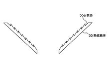
図4は熱遮蔽体の断面の模式図である。
熱遮蔽体55において、単結晶シリコン58側の表面55aは凹凸状である。凹凸の高低差は熱遮蔽体55の表面55aに沿って落ちる塵を留められる程度である。具体的には、0.5〜10.0mm程度である。
FIG. 4 is a schematic view of a cross section of the heat shield.
In the heat shield 55, the surface 55a on the single crystal silicon 58 side is uneven. The level difference of the unevenness is such that dust falling along the surface 55a of the heat shield 55 can be retained. Specifically, it is about 0.5 to 10.0 mm.
本実施形態によれば、炉体内上部から熱遮蔽体に落下する塵及び熱遮蔽体上の塵を熱遮蔽体に留めることができる。よって熱遮蔽体からシリコン融液への塵の落下が低減され、単結晶シリコンの品質低下が防止される。 According to this embodiment, dust falling on the heat shield from the upper part of the furnace body and dust on the heat shield can be retained on the heat shield. Therefore, the fall of the dust from the heat shield to the silicon melt is reduced, and the deterioration of the quality of the single crystal silicon is prevented.
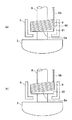
ところで図6で示されるように、実際の冷却コイル6は単結晶シリコン8の引き上げ経路を略中心にして螺旋状に巻かれた冷却パイプ6bを有する。この冷却パイプ6bの内部には冷却媒体である冷却水が、図示しない冷却水供給機構から供給される。このように冷却パイプ6bを螺旋状にして筒状の冷却コイル6を形成した場合に、冷却コイル6の下端6aは平坦にならず、最大でパイプ1本分の高低差L1−L2が生じる。このため冷却コイル6の下端6aと熱遮蔽体5との間隙は場所によって異なることになり、ガス流れの速い箇所と遅い箇所が発生してガス流れの不均一化が発生する。このように冷却コイル6の下端6aと熱遮蔽体5との間隙でガス流れが不均一化すると、単結晶シリコン8の引き上げに伴いガス流れが変化する際に、炉体内の上部に堆積した微小な塵(カーボン等)の落下を誘発することがある。
Incidentally, as shown in FIG. 6, the
本実施形態では、こうした高低差に起因する塵の落下を防止するために、図7(a)で示されるように、冷却コイル6の下端6aの一部に沿ってコイル補完部材61が取り付けられている。コイル補完部材61は冷却コイル6の曲率と同じ曲率を有する。冷却コイル6とコイル補完部材61とは一体化され、ここでは一体化された構造体をコイル体60と称する。コイル補完部材61は冷却コイル6における下端6aの高低差を補完して、コイル体60の下端を略平坦にする。コイル補完部材61の材料は、単結晶シリコン8の形成や品質に支障をきたすことがないのであれば、どのようなものでもよい。
In the present embodiment, in order to prevent the dust from falling due to such a height difference, a
図7(a)で示されるように、冷却コイル6における下端6aの一部にコイル補完部材61が取り付けられるのではなく、図7(b)で示されるように、冷却コイル6における下端6aの全体にコイル補完部材62が取り付けられてもよい。
As shown in FIG. 7A, the
また本実施形態では、コイル補完部材61を筒状の冷却パイプ6に設けているが、これに限らず、コイル補完部材61を螺旋状のパイプに温度調整媒体を流す筒状のコイルに設けてもよい。
In this embodiment, the
本実施形態によれば、冷却コイルのような温度調整コイルの下端にコイル補完部材を取り付けてコイル体を形成するため、コイル体の下端と熱遮蔽体との間隙を全ての部分で一定にすることができる。したがってコイル体と熱遮蔽体との間隙でガス流れの不均一化が発生しなくなる。よって炉体内の上部に堆積した微小な塵の落下を誘発することがなくなり、シリコン融液への塵の落下が低減され、単結晶シリコンの品質低下が防止される。 According to this embodiment, a coil complement member is attached to the lower end of a temperature adjustment coil such as a cooling coil to form a coil body, so that the gap between the lower end of the coil body and the heat shield is constant in all parts. be able to. Therefore, nonuniform gas flow does not occur in the gap between the coil body and the heat shield. Therefore, it does not induce the fall of the minute dust deposited on the upper part of the furnace body, the fall of the dust to the silicon melt is reduced, and the quality deterioration of the single crystal silicon is prevented.
1 炉体
5、45、55 熱遮蔽体
6 冷却コイル
8 単結晶シリコン
10 単結晶引き上げ装置
60 コイル体
61 コイル補完部材
DESCRIPTION OF SYMBOLS 1
Claims (4)
単結晶シリコンの側面と筒状体の内壁面とで形成される環状空間のうち、結晶の引き上げ軸と直交する平面に含まれる断面部分の面積をS1とし、且つ筒状体の下端から下方に延在する筒状空間のうち、筒状体と熱遮蔽体との間に位置する部分の側面の面積をS2とした場合に、S2/S1が1.15未満であること
を特徴とする単結晶シリコン引き上げ装置。 A cylindrical body surrounding the single crystal silicon pulling path; an upper part surrounding the cylindrical body; and a lower part surrounding the single crystal silicon pulling path below the cylindrical body; In the single crystal silicon pulling apparatus that pulls up the single crystal silicon while supplying the gas from the top to the bottom of the furnace with a heat shield having an inner diameter equal to or less than the inner diameter of the cylindrical body ,
Of the annular space formed by the side surface of the single crystal silicon and the inner wall surface of the cylindrical body, the area of the cross-sectional portion included in the plane orthogonal to the crystal pulling axis is S1, and downward from the lower end of the cylindrical body. Of the extending cylindrical space, S2 / S1 is less than 1.15 when the area of the side surface of the portion located between the cylindrical body and the heat shield is S2. Crystalline silicon pulling device.
単結晶シリコンの側面と筒状体の内壁面とで形成される環状空間のうち、結晶の引き上げ軸と直交する平面に含まれる断面部分の面積をS1とし、且つ筒状体の下端から下方に延在する筒状空間のうち、筒状体と熱遮蔽体との間に位置する部分の側面の面積をS2とした場合に、筒状体の下端と熱遮蔽体との間を通過するガスによってシリコン融液への塵の落下を防止できるようなS2/S1の値を求めておき、
単結晶シリコンの引き上げ時にS2/S1が求めた値になるように単結晶シリコンの引き上げ経路と筒状体と熱遮蔽体の相対的な位置を調整すること
を特徴とするシリコン融液の汚染防止方法。 A cylindrical body surrounding the single crystal silicon pulling path; an upper part surrounding the cylindrical body; and a lower part surrounding the single crystal silicon pulling path below the cylindrical body; A single crystal silicon pulling device equipped with a heat shield having an inner diameter equal to or smaller than the inner diameter of the cylindrical body, and a silicon melt that prevents dust from falling into the silicon melt by the gas descending from above the furnace. In the method of preventing liquid contamination,
Of the annular space formed by the side surface of the single crystal silicon and the inner wall surface of the cylindrical body, the area of the cross-sectional portion included in the plane orthogonal to the crystal pulling axis is S1, and downward from the lower end of the cylindrical body. Gas that passes between the lower end of the tubular body and the heat shield when the area of the side surface of the portion located between the tubular body and the heat shield in the extending tubular space is S2. The value of S2 / S1 that can prevent the dust from dropping into the silicon melt is obtained,
Contamination prevention of the silicon melt characterized by adjusting the single crystal silicon pulling path and the relative position of the cylindrical body and the heat shield so that S2 / S1 becomes the value obtained when pulling the single crystal silicon Method.
単結晶シリコンの側面と筒状体の内壁面とで形成される環状空間のうち、結晶の引き上げ軸と直交する平面に含まれる断面部分の面積をS1とし、且つ筒状体の下端から下方に延在する筒状空間のうち、筒状体と熱遮蔽体との間に位置する部分の側面の面積をS2とした場合に、S2/S1を1.15未満とするように単結晶シリコンの引き上げ経路と筒状体と熱遮蔽体の相対的な位置を調整すること
を特徴とするシリコン融液の汚染防止方法。 A cylindrical body surrounding the single crystal silicon pulling path; an upper part surrounding the cylindrical body; and a lower part surrounding the single crystal silicon pulling path below the cylindrical body; A single crystal silicon pulling device equipped with a heat shield having an inner diameter equal to or less than the inner diameter of the cylindrical body, and a silicon melt that prevents dust from falling into the silicon melt due to gas descending from above the furnace. In the method of preventing liquid contamination,
Of the annular space formed by the side surface of the single crystal silicon and the inner wall surface of the cylindrical body, the area of the cross-sectional portion included in the plane orthogonal to the crystal pulling axis is S1, and downward from the lower end of the cylindrical body. Of the extending cylindrical space, when the area of the side surface of the portion located between the cylindrical body and the heat shield is S2, the single crystal silicon is made so that S2 / S1 is less than 1.15. A method for preventing contamination of silicon melt, comprising adjusting a relative position of a pulling path, a cylindrical body, and a heat shield.
温度調整用の媒体が供給されるパイプが単結晶シリコンの引き上げ経路を略中心にして螺旋状に巻かれてなる温度調整コイルと、 A temperature adjusting coil in which a pipe to which a temperature adjusting medium is supplied is spirally wound around a single crystal silicon pulling path;
前記温度調整コイル下端の全体又は一部に沿って取り付けられて該温度調整コイルと共にコイル体を形成するコイル補完部材と、を有し、 A coil complementary member that is attached along all or part of the lower end of the temperature adjustment coil and forms a coil body together with the temperature adjustment coil, and
前記コイル体下端のいずれの部分と前記熱遮蔽体との間隙が一定であること The gap between any part of the lower end of the coil body and the heat shield is constant.
を特徴とする請求項1記載の単結晶シリコン引き上げ装置。 The single crystal silicon pulling apparatus according to claim 1.
Priority Applications (9)
| Application Number | Priority Date | Filing Date | Title |
|---|---|---|---|
| JP2005279979A JP4349493B2 (en) | 2005-09-27 | 2005-09-27 | Single crystal silicon pulling apparatus, silicon melt contamination prevention method, and silicon melt contamination prevention apparatus |
| DE112006004261.0T DE112006004261B4 (en) | 2005-09-27 | 2006-06-27 | Device for preventing contamination of silicon melt |
| US11/992,278 US8404046B2 (en) | 2005-09-27 | 2006-06-27 | Single crystal silicon pulling apparatus, method for preventing contamination of silicon melt, and device for preventing contamination of silicon melt |
| KR1020137007398A KR101311911B1 (en) | 2005-09-27 | 2006-06-27 | Single crystal silicon pulling apparatus, method for preventing contamination of silicon melt, and apparatus for preventing contamination of silicon melt |
| PCT/JP2006/312791 WO2007037052A1 (en) | 2005-09-27 | 2006-06-27 | Single crystal silicon pulling apparatus, method for preventing contamination of silicon melt, and apparatus for preventing contamination of silicon melt |
| DE112006002580.5T DE112006002580B4 (en) | 2005-09-27 | 2006-06-27 | Single crystal silicon pulling apparatus and method for preventing contamination of silicon melt |
| KR1020087007391A KR101327064B1 (en) | 2005-09-27 | 2006-06-27 | Single crystal silicon pulling apparatus, method for preventing contamination of silicon melt, and apparatus for preventing contamination of silicon melt |
| TW095124451A TW200714753A (en) | 2005-09-27 | 2006-07-05 | Single crystal silicon pulling apparatus, method for preventing contamination of silicon melt, and apparatus for preventing contamination of silicon melt |
| US13/474,268 US9080251B2 (en) | 2005-09-27 | 2012-05-17 | Single crystal silicon pulling device, method for preventing contamination of silicon melt, and device for preventing contamination of silicon melt |
Applications Claiming Priority (1)
| Application Number | Priority Date | Filing Date | Title |
|---|---|---|---|
| JP2005279979A JP4349493B2 (en) | 2005-09-27 | 2005-09-27 | Single crystal silicon pulling apparatus, silicon melt contamination prevention method, and silicon melt contamination prevention apparatus |
Related Child Applications (1)
| Application Number | Title | Priority Date | Filing Date |
|---|---|---|---|
| JP2009091118A Division JP4499178B2 (en) | 2009-04-03 | 2009-04-03 | Silicon melt contamination prevention device |
Publications (2)
| Publication Number | Publication Date |
|---|---|
| JP2007091493A JP2007091493A (en) | 2007-04-12 |
| JP4349493B2 true JP4349493B2 (en) | 2009-10-21 |
Family
ID=37899488
Family Applications (1)
| Application Number | Title | Priority Date | Filing Date |
|---|---|---|---|
| JP2005279979A Active JP4349493B2 (en) | 2005-09-27 | 2005-09-27 | Single crystal silicon pulling apparatus, silicon melt contamination prevention method, and silicon melt contamination prevention apparatus |
Country Status (6)
| Country | Link |
|---|---|
| US (2) | US8404046B2 (en) |
| JP (1) | JP4349493B2 (en) |
| KR (2) | KR101327064B1 (en) |
| DE (2) | DE112006002580B4 (en) |
| TW (1) | TW200714753A (en) |
| WO (1) | WO2007037052A1 (en) |
Families Citing this family (6)
| Publication number | Priority date | Publication date | Assignee | Title |
|---|---|---|---|---|
| JP5186970B2 (en) * | 2008-03-24 | 2013-04-24 | 信越半導体株式会社 | Single crystal manufacturing apparatus and method |
| KR101871059B1 (en) * | 2016-11-17 | 2018-07-20 | 에스케이실트론 주식회사 | Single crystal ingot growing apparatus |
| JP6760128B2 (en) | 2017-02-24 | 2020-09-23 | 株式会社Sumco | Silicon single crystal manufacturing method, rectifying member, and single crystal pulling device |
| DE102017220352B4 (en) | 2017-11-15 | 2023-02-02 | Siltronic Ag | Method for inspecting an apparatus for pulling a single crystal and apparatus for pulling a single crystal |
| DE102018217509A1 (en) * | 2018-10-12 | 2020-04-16 | Siltronic Ag | Device for pulling a single crystal of semiconductor material according to the CZ method from a melt and method using the device |
| CN111663178A (en) * | 2019-03-08 | 2020-09-15 | 宁夏隆基硅材料有限公司 | Heat shield device for pulling single crystal and single crystal silicon production equipment |
Family Cites Families (19)
| Publication number | Priority date | Publication date | Assignee | Title |
|---|---|---|---|---|
| JPH04209789A (en) * | 1990-11-30 | 1992-07-31 | Toshiba Ceramics Co Ltd | Apparatus for pulling up silicon single crystal |
| JP2783049B2 (en) * | 1992-02-28 | 1998-08-06 | 信越半導体株式会社 | Method and apparatus for manufacturing single crystal silicon rod |
| JP2952733B2 (en) * | 1992-10-09 | 1999-09-27 | コマツ電子金属株式会社 | Silicon single crystal manufacturing method |
| JP2807609B2 (en) * | 1993-01-28 | 1998-10-08 | 三菱マテリアルシリコン株式会社 | Single crystal pulling device |
| DE19503357A1 (en) * | 1995-02-02 | 1996-08-08 | Wacker Siltronic Halbleitermat | Device for producing a single crystal |
| JP2937109B2 (en) * | 1996-02-29 | 1999-08-23 | 住友金属工業株式会社 | Single crystal manufacturing apparatus and manufacturing method |
| JP3992800B2 (en) * | 1997-09-22 | 2007-10-17 | Sumco Techxiv株式会社 | Single crystal manufacturing apparatus and single crystal manufacturing method |
| JP4195738B2 (en) * | 1998-04-08 | 2008-12-10 | Sumco Techxiv株式会社 | Single crystal manufacturing equipment |
| JP3747696B2 (en) * | 1999-07-23 | 2006-02-22 | 株式会社Sumco | Heat shielding member of silicon single crystal pulling device |
| TW588127B (en) * | 2000-02-01 | 2004-05-21 | Komatsu Denshi Kinzoku Kk | Apparatus for pulling single crystal by CZ method |
| JP3573045B2 (en) * | 2000-02-08 | 2004-10-06 | 三菱住友シリコン株式会社 | Manufacturing method of high quality silicon single crystal |
| US6277351B1 (en) * | 2000-03-20 | 2001-08-21 | Carl Francis Swinehart | Crucible for growing macrocrystals |
| US6482263B1 (en) | 2000-10-06 | 2002-11-19 | Memc Electronic Materials, Inc. | Heat shield assembly for crystal pulling apparatus |
| KR100805518B1 (en) * | 2001-01-26 | 2008-02-20 | 엠이엠씨 일렉트로닉 머티리얼즈 인코포레이티드 | Low defect density silicon having a vacancy-dominated core substantially free of oxidation induced stacking faults |
| JP2002321997A (en) * | 2001-04-20 | 2002-11-08 | Shin Etsu Handotai Co Ltd | Apparatuses for making silicon single crystal and method for making silicon single crystal using the same |
| JP5086504B2 (en) | 2001-05-28 | 2012-11-28 | 東日本メディコム株式会社 | IC card insurance card system using mobile phone |
| KR100445188B1 (en) | 2001-08-31 | 2004-08-18 | 주식회사 실트론 | Coating material for absorbing a radiation energy, the method thereof, the apparatus for cooling, and growing a single crystaline silicon ingot |
| WO2003027434A1 (en) * | 2001-09-26 | 2003-04-03 | Bakke Technology As | Arrangement in a gripper mechanism for a free pipe/rodlike end portion of a downhole tool |
| KR100486876B1 (en) | 2002-12-03 | 2005-05-03 | 주식회사 실트론 | An apparatus for growing silicon single crystals |
-
2005
- 2005-09-27 JP JP2005279979A patent/JP4349493B2/en active Active
-
2006
- 2006-06-27 WO PCT/JP2006/312791 patent/WO2007037052A1/en active Application Filing
- 2006-06-27 US US11/992,278 patent/US8404046B2/en active Active
- 2006-06-27 DE DE112006002580.5T patent/DE112006002580B4/en active Active
- 2006-06-27 KR KR1020087007391A patent/KR101327064B1/en active IP Right Grant
- 2006-06-27 DE DE112006004261.0T patent/DE112006004261B4/en active Active
- 2006-06-27 KR KR1020137007398A patent/KR101311911B1/en active IP Right Grant
- 2006-07-05 TW TW095124451A patent/TW200714753A/en unknown
-
2012
- 2012-05-17 US US13/474,268 patent/US9080251B2/en active Active
Also Published As
| Publication number | Publication date |
|---|---|
| KR20130045932A (en) | 2013-05-06 |
| US9080251B2 (en) | 2015-07-14 |
| TWI324642B (en) | 2010-05-11 |
| KR101311911B1 (en) | 2013-09-27 |
| US8404046B2 (en) | 2013-03-26 |
| KR101327064B1 (en) | 2013-11-07 |
| KR20080042146A (en) | 2008-05-14 |
| WO2007037052A1 (en) | 2007-04-05 |
| DE112006004261A5 (en) | 2012-09-20 |
| DE112006002580B4 (en) | 2017-02-23 |
| JP2007091493A (en) | 2007-04-12 |
| DE112006004261B4 (en) | 2017-04-13 |
| US20090229512A1 (en) | 2009-09-17 |
| TW200714753A (en) | 2007-04-16 |
| DE112006002580T5 (en) | 2008-08-14 |
| US20120222613A1 (en) | 2012-09-06 |
Similar Documents
| Publication | Publication Date | Title |
|---|---|---|
| JP4349493B2 (en) | Single crystal silicon pulling apparatus, silicon melt contamination prevention method, and silicon melt contamination prevention apparatus | |
| TWI759399B (en) | Crystal pulling system and method including crucible and conditioning members | |
| US9217208B2 (en) | Apparatus for producing single crystal | |
| JP6317374B2 (en) | Gas doping system for controlled doping of melts of semiconductor grade materials or solar grade materials | |
| EP3619339A1 (en) | Crystal pulling system and method including crucible and barrier | |
| JP6202119B2 (en) | Method for producing silicon single crystal | |
| KR101385997B1 (en) | Apparatus for producing single crystal and method for producing single crystal | |
| JP2016509989A5 (en) | ||
| TWI598475B (en) | Weir for improved crystal growth in a continuous czochralski process | |
| KR101381326B1 (en) | Method for producing semiconductor wafers composed of silicon | |
| JP2010018446A (en) | Method for producing single crystal and single crystal pulling apparatus | |
| JP4499178B2 (en) | Silicon melt contamination prevention device | |
| KR101279390B1 (en) | Apparatus for growing single crystal ingot and method for spraying gas in ingot growing apparatus | |
| JP5415052B2 (en) | Ultra-low defect semiconductor single crystal manufacturing method and manufacturing apparatus thereof | |
| JP2007186356A (en) | Apparatus and method for producing single crystal | |
| JP2009184863A (en) | Apparatus and method for manufacturing single crystal | |
| JP2007204332A (en) | Device and method for manufacturing single crystal | |
| JP2007204305A (en) | Single crystal pulling apparatus | |
| JP2007182355A (en) | Heat shielding member of silicon single crystal pulling apparatus | |
| JP2009274920A (en) | Production method of silicon single crystal | |
| JP2011026147A (en) | Silicon single crystal pulling device | |
| JP2018188338A (en) | Production method of silicon single crystal, and silicon single crystal | |
| JP6658780B2 (en) | Heat shielding member, single crystal pulling apparatus, and method for manufacturing single crystal silicon ingot | |
| JP6563459B2 (en) | Gas doping system for controlled doping of melts of semiconductor grade materials or solar grade materials | |
| JPH07300389A (en) | Production of semiconductor single crystal |
Legal Events
| Date | Code | Title | Description |
|---|---|---|---|
| A621 | Written request for application examination |
Free format text: JAPANESE INTERMEDIATE CODE: A621 Effective date: 20080813 |
|
| A131 | Notification of reasons for refusal |
Free format text: JAPANESE INTERMEDIATE CODE: A131 Effective date: 20090203 |
|
| A521 | Request for written amendment filed |
Free format text: JAPANESE INTERMEDIATE CODE: A523 Effective date: 20090317 |
|
| TRDD | Decision of grant or rejection written | ||
| A01 | Written decision to grant a patent or to grant a registration (utility model) |
Free format text: JAPANESE INTERMEDIATE CODE: A01 Effective date: 20090707 |
|
| A01 | Written decision to grant a patent or to grant a registration (utility model) |
Free format text: JAPANESE INTERMEDIATE CODE: A01 |
|
| A61 | First payment of annual fees (during grant procedure) |
Free format text: JAPANESE INTERMEDIATE CODE: A61 Effective date: 20090714 |
|
| FPAY | Renewal fee payment (event date is renewal date of database) |
Free format text: PAYMENT UNTIL: 20120731 Year of fee payment: 3 |
|
| R150 | Certificate of patent or registration of utility model |
Ref document number: 4349493 Country of ref document: JP Free format text: JAPANESE INTERMEDIATE CODE: R150 Free format text: JAPANESE INTERMEDIATE CODE: R150 |
|
| FPAY | Renewal fee payment (event date is renewal date of database) |
Free format text: PAYMENT UNTIL: 20120731 Year of fee payment: 3 |
|
| FPAY | Renewal fee payment (event date is renewal date of database) |
Free format text: PAYMENT UNTIL: 20130731 Year of fee payment: 4 |
|
| R250 | Receipt of annual fees |
Free format text: JAPANESE INTERMEDIATE CODE: R250 |
|
| R250 | Receipt of annual fees |
Free format text: JAPANESE INTERMEDIATE CODE: R250 |
|
| R250 | Receipt of annual fees |
Free format text: JAPANESE INTERMEDIATE CODE: R250 |
|
| R250 | Receipt of annual fees |
Free format text: JAPANESE INTERMEDIATE CODE: R250 |
|
| R250 | Receipt of annual fees |
Free format text: JAPANESE INTERMEDIATE CODE: R250 |
|
| R250 | Receipt of annual fees |
Free format text: JAPANESE INTERMEDIATE CODE: R250 |
|
| R250 | Receipt of annual fees |
Free format text: JAPANESE INTERMEDIATE CODE: R250 |
|
| R250 | Receipt of annual fees |
Free format text: JAPANESE INTERMEDIATE CODE: R250 |
|
| R250 | Receipt of annual fees |
Free format text: JAPANESE INTERMEDIATE CODE: R250 |
|
| R250 | Receipt of annual fees |
Free format text: JAPANESE INTERMEDIATE CODE: R250 |
|
| R250 | Receipt of annual fees |
Free format text: JAPANESE INTERMEDIATE CODE: R250 |
|
| R250 | Receipt of annual fees |
Free format text: JAPANESE INTERMEDIATE CODE: R250 |