JP4299387B2 - Radio wave absorber assembly member and radio wave absorber manufacturing method - Google Patents
Radio wave absorber assembly member and radio wave absorber manufacturing method Download PDFInfo
- Publication number
- JP4299387B2 JP4299387B2 JP29762498A JP29762498A JP4299387B2 JP 4299387 B2 JP4299387 B2 JP 4299387B2 JP 29762498 A JP29762498 A JP 29762498A JP 29762498 A JP29762498 A JP 29762498A JP 4299387 B2 JP4299387 B2 JP 4299387B2
- Authority
- JP
- Japan
- Prior art keywords
- radio wave
- wave absorber
- base material
- combustible
- fixed
- Prior art date
- Legal status (The legal status is an assumption and is not a legal conclusion. Google has not performed a legal analysis and makes no representation as to the accuracy of the status listed.)
- Expired - Fee Related
Links
Images


Classifications
-
- H—ELECTRICITY
- H05—ELECTRIC TECHNIQUES NOT OTHERWISE PROVIDED FOR
- H05K—PRINTED CIRCUITS; CASINGS OR CONSTRUCTIONAL DETAILS OF ELECTRIC APPARATUS; MANUFACTURE OF ASSEMBLAGES OF ELECTRICAL COMPONENTS
- H05K9/00—Screening of apparatus or components against electric or magnetic fields
- H05K9/0001—Rooms or chambers
- H05K9/0003—Shielded walls, floors, ceilings, e.g. wallpaper, wall panel, electro-conductive plaster, concrete, cement, mortar
-
- H—ELECTRICITY
- H01—ELECTRIC ELEMENTS
- H01Q—ANTENNAS, i.e. RADIO AERIALS
- H01Q17/00—Devices for absorbing waves radiated from an antenna; Combinations of such devices with active antenna elements or systems
-
- H—ELECTRICITY
- H01—ELECTRIC ELEMENTS
- H01Q—ANTENNAS, i.e. RADIO AERIALS
- H01Q17/00—Devices for absorbing waves radiated from an antenna; Combinations of such devices with active antenna elements or systems
- H01Q17/008—Devices for absorbing waves radiated from an antenna; Combinations of such devices with active antenna elements or systems with a particular shape
-
- Y—GENERAL TAGGING OF NEW TECHNOLOGICAL DEVELOPMENTS; GENERAL TAGGING OF CROSS-SECTIONAL TECHNOLOGIES SPANNING OVER SEVERAL SECTIONS OF THE IPC; TECHNICAL SUBJECTS COVERED BY FORMER USPC CROSS-REFERENCE ART COLLECTIONS [XRACs] AND DIGESTS
- Y10—TECHNICAL SUBJECTS COVERED BY FORMER USPC
- Y10T—TECHNICAL SUBJECTS COVERED BY FORMER US CLASSIFICATION
- Y10T428/00—Stock material or miscellaneous articles
- Y10T428/24—Structurally defined web or sheet [e.g., overall dimension, etc.]
- Y10T428/24149—Honeycomb-like
-
- Y—GENERAL TAGGING OF NEW TECHNOLOGICAL DEVELOPMENTS; GENERAL TAGGING OF CROSS-SECTIONAL TECHNOLOGIES SPANNING OVER SEVERAL SECTIONS OF THE IPC; TECHNICAL SUBJECTS COVERED BY FORMER USPC CROSS-REFERENCE ART COLLECTIONS [XRACs] AND DIGESTS
- Y10—TECHNICAL SUBJECTS COVERED BY FORMER USPC
- Y10T—TECHNICAL SUBJECTS COVERED BY FORMER US CLASSIFICATION
- Y10T428/00—Stock material or miscellaneous articles
- Y10T428/24—Structurally defined web or sheet [e.g., overall dimension, etc.]
- Y10T428/2419—Fold at edge
Description
【0001】
【発明の属する技術分野】
本発明は、電波暗室に使用する電波吸収体に関する。
【0002】
【従来の技術】
近年、より高度な情報社会の実現に向けて、移動通信分野を中心に電波利用が急速に拡大している。また、今日のマイクロエレクトロニクス技術の革新的進歩に伴って多様な電子機器が普及している。しかし、このような情報通信技術の発達に伴い、不要な電磁波ノイズ等が精密機器関連装置に及ぼす影響が問題となっている。
【0003】
電磁波ノイズの測定には、通常、電磁波の反射のない電波暗室(電波無響室)が使用され、このような電波暗室の内壁には電波吸収体が配設されている。電波暗室に使用される従来の電波吸収体としては、導電性を得るためにカーボンブラック等が配合された発泡スチロール、発泡スチレンや発泡ウレタン等の有機系の材料からなる電波吸収体が挙げられる。また、電波吸収体は、四角錐形状、三角柱形状、楔形状の立体的構造体として使用される。このような立体的構造をとる電波吸収体は、例えば、発泡前のポリスチロール粒子を直径数mmの球状に予備発泡させ、この表面にカーボンブラック等の導電性材料の粉末をコーティングした後、これを所望の型に入れて加熱し第2次発泡させることにより製造することが一般的である。
【0004】
また、電波吸収性を有する熱可塑性合成樹脂により形成された被組立部材を、所定の折曲部を局部的に加熱し軟化させた後、この折曲部で折り曲げて所望の形状の電波吸収体を製造する方法が提案されている(特許第2760578号)。
【0005】
【発明が解決しようとする課題】
しかしながら、ポリスチロール、ポリスチレン、ポリウレタン等の有機系の材料を加熱発泡させる方法により製造された四角錐形状、三角柱形状、楔形状の電波吸収体は、電波暗室の施工の際の搬入時にかさばるだけでなく、接触等による破損を生じやすいという問題がある。
【0006】
また、特許第2760578号に記載の製造方法では、所定の折曲部を局部的に加熱し軟化させる処理を施す必要があり、作業が煩雑であるという問題がある。さらに、熱可塑性合成樹脂を用いているため、イミュニティ試験等の大電力の試験を行う電波暗室では、不燃性、耐火性に劣り安全性の面で問題がある。
【0007】
本発明は、上記のような実情に鑑みてなされたものであり、電波暗室の施工時の作業性に優れ、かつ、不燃性を有する所望の形状の電波吸収体を容易に製造することができる製造方法とこれに使用できる電波吸収体組立用部材とを提供することを目的とする。
【0008】
【課題を解決するための手段】
このような目的を達成するために、本発明の電波吸収体組立用部材は、所望形状の構造体を組み立て可能な不燃性の基材と、該基材の所定部位に固着された電波吸収性の不燃性材とを備え、前記基材は、前記不燃性材が固着されていない部位に折り曲げ用の溝部を備えるような構成とした。
【0010】
また、本発明の電波吸収体組立用部材は、前記基材が複数の基材の前記不燃性材が固着されていない部位を折り曲げ可能な接合部材によって接合した連結体であるような構成とした。
【0011】
また、本発明の電波吸収体組立用部材は、前記不燃性材が含水無機化合物と導電性材料を含むスラリーから抄造した不燃性シートを無機接着剤を使用してハニカム形状に積層したハニカム構造体であるような構成とした。
【0012】
さらに、本発明の電波吸収体組立用部材は、前記不燃性材が導電性材料を含有する導電層を表面に備えるような構成とした。
【0013】
本発明の電波吸収体の製造方法は、不燃性の基材を所望形状の構造体が組み立て可能な形状に加工し該基材の所定部位に電波吸収性の不燃性材を固着して電波吸収体組立用部材を作製し、前記基材の不燃性材が固着されていない部位に予め折り曲げ用の溝部を形成し、該溝部で前記基材を折り曲げ、前記基材の端部同士を接合するような構成とした。
【0014】
本発明の電波吸収体の製造方法は、所望形状に加工した不燃性の基材の所定部位に電波吸収性の不燃性材を固着したものであって、前記基材の不燃性材が固着されていない部位に予め折り曲げ用の溝部を形成しものを複数成形し、これらを直接または不燃性材を固着していない不燃性の基材を介して、折り曲げ可能な接合部材によって接合して電波吸収体組立用部材を作製し、その後、前記接合部材を折り曲げ、前記基材の端部同士を接合するような構成とした。
【0015】
また、本発明の電波吸収体の製造方法は、前記電波吸収体の形状が四角錐形状、三角柱形状および楔形状のいずれかであるような構成とした。
【0017】
このような本発明では、電波吸収体組立用部材は平面形状であるためかさばることがなく取り扱いが容易であり、電波吸収体組立用部材の不燃性の基材を折り曲げて所望の構造体を作製することにより、あるいは、電波吸収体組立用部材を接合部材で折り曲げて所望の構造体を作製することにより、この構造体の所定部位に電波吸収性の不燃性材が固着された電波吸収体を得ることができる。
【0018】
【発明の実施の形態】
以下、本発明の実施の形態について説明する。
第1の実施形態
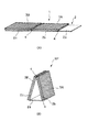
図1は本発明の電波吸収体組立用部材と、これを用いて製造した電波吸収体の一実施形態を示す斜視図である。図1(A)において、電波吸収体組立用部材1は不燃性の基材2と、この基材2上に固着された電波吸収性の不燃性材3A,3Bとを備えている。ここで、本発明中でいう「不燃性」とは、750℃の炉内に20分間置いた場合に炉内温度の上昇が50℃以下であれば不燃材料と判定する建築材料試験法(建設省告示第1828号)に合格するものを意味する。また、「電波吸収性」とは、反射減衰量が約20dB以上の値を有するものを意味する。
【0019】
基材2は、不燃性材が設けられていない領域2aと、不燃性材3A,3Bが固着されている領域2b,2cとからなり、領域2aと領域2bとの境界、および、領域2bと領域2cとの境界には、それぞれ折り曲げ用の溝部4が設けられている。この基材2は、上記の溝部4において折り曲げることにより、楔形状の構造体を組み立てることができる。図2は基材2上への不燃性材3Aの固着を説明する部分斜視図である。図2(A)に示されるように、予め溝部4が設けられた基材2を準備し、この基材2の領域2b上に、不燃性材3Aの端部を溝部4の端部に一致させるように固着する(図2(B))。基材への不燃性材の固着は、例えば、ポルトランドセメント、石膏等の水和反応によって硬化する接着剤、あるいは、リン酸塩、シリカゾル、水ガラス組成物等の無機接着剤等を使用することができる。
【0020】
電波吸収体組立用部材1を構成する不燃性の基材2としては、例えば、セラミックス繊維不織布からなる成形体、ガラス繊維不織布からなる成形体、ケイ酸カルシウムボード、炭酸カルシウム発泡体ボード、不燃紙、不燃紙同志を無機接着剤を介して接着した積層体を加圧成形したもの等が挙げられる。これらのなかで、折り曲げ位置の溝部4の形成の容易さ、折り曲げ作業の容易さ、折り曲げ作業に対する基材2の耐久性等から、不燃紙同志を無機接着剤を介して接着した積層体を加圧成形したものが特に好ましい。
【0021】
また、本発明では、不燃性の基材2に軽量化および放熱性向上を目的として、基材2の機械的強度が実用上問題のない範囲で開口部を設けてもよい。図3は、このような不燃性の基材2の一例を示す部分斜視図であり、不燃性材3Aが固着される領域2bに複数の開口部5が設けられている。開口部5の形状、位置、数等は、基材2の機械的強度を考慮して適宜設定することができる。
【0022】
上述のような不燃性の基材2への折り曲げ用の溝部4の形成は、例えば、断面V字形状の型を押圧する方法、回転刃で切削形成する方法等、いずれであってもよい。形成する溝部4の数は、図示のように1か所に1本でもよく、平行に複数本形成してもよい。また、図4に示されるように、基材2を構成する基材(領域)2aと基材(領域)2bのつき合わせ部に溝つきの接合部材6を固着してもよい。溝つきの接合部材6としては、難燃性繊維、ガラス繊維等を無機接着剤を用いて成形したものを使用することができる。尚、図4に示される例では、基材2の両面を溝つきの接合部材6で接合しているが、不燃性材の固着位置等に応じて片面のみで接合してもよい。
【0023】
上記の不燃性の基材2の厚みは0.3〜10mm、折り曲げ用の溝部4の深さは0.1〜6mm程度とすることができ、好ましくは、基材2の厚みが0.5〜3mm、折り曲げ用の溝部4の深さが0.1〜1mm程度である。
【0024】
電波吸収体組立用部材1を構成する電波吸収性の不燃性材3A,3Bは、その基材2への固着面が基材2の領域2b,2cの形状と略同形状となるように形成されている。不燃性材3A,3Bとしては、例えば、多数の独立気泡性の無機粒子を、導電性材料を分散含有した無機接着剤によって集積結合して作製した電波吸収体(特許第2743227号)、特定のアスペクト比を有するセラミックス短繊維やガラス短繊維からなる成形体に導電性材料を浸透含浸で付着固定させた電波吸収体(特開平9−307268号公報)、セメント、軽量骨材、非導電性繊維、合成樹脂エマルジョン、導電性材料とで構成した組成物からなる電波吸収体(特開平8−97544号)、含水無機化合物と導電性材料を含むスラリーから抄造した不燃性シートを無機接着剤を使用してハニカム形状に積層した不燃性のハニカム構造体からなる電波吸収体等を用いることができる。このなかで、電波吸収特性、軽量性、不燃性、機械的強度、放熱性の観点から、不燃性ハニカム構造体が好ましい。
【0025】
上記の導電性材料としては、カーボンブラック、グラファイト、炭素繊維等を使用することができる。独立気泡性の無機粒子としては、シラスバルーン、シリカバルーン、ガラスビーズ、パーライトおよびアルミナシリカバルーン等を使用することができる。また、無機接着剤は、ポルトランドセメント、石膏等の水和反応によって硬化する接着剤、あるいは、リン酸塩、シリカゾル、水ガラス組成物等の無機接着剤等を使用することができ、特に安価で結合性の高い水ガラス組成物が好ましく使用できる。水ガラスはアルカリ金属ケイ酸塩を主成分とする水性溶液であり、特にケイ酸ナトリウムは安価でJIS規格品として入手が容易であり好ましい。また、ケイ酸ナトリウムの水ガラスにケイ酸リチウムの水ガラスを混合して用いてもよい。
【0026】
不燃性材3A,3Bとしてのハニカム構造体の作製は、まず、所定幅の不燃性シートの長さ方向に所定の間隔で線状に無機接着剤を塗布し、かつ、隣接する不燃シートの間で線状の無機接着剤の塗布位置を半ピッチずらすようにして、所定枚数の不燃性シートを積層する。そして、この積層体を圧着して無機接着剤塗布部位で接合することによりシートブロックとする。ここでは、上記の無機接着剤の塗布幅が、ハニカム構造体のセルの重合面の長さ寸法となり、この無機接着剤層の幅と形成間隔を調整することにより、セルサイズを制御することができる。次に、上記のシートブロックを所望のハニカム構造体の厚みに裁断し、無機含浸剤に浸漬しながら展張させ、セルを形成する所望の展張状態で無機含浸剤を乾燥固化して無機含浸剤層とすることにより、ハニカム構造体が得られる。使用する無機接着剤としては、例えば、リン酸アルミニウム溶液、コロイダルシリカ、コロイダルアルミナ等に硬化剤、触媒等を混合した水溶性または水分散タイプのものを挙げることができる。また、無機含浸剤としては、各種の無機接着剤を使用することができるが、不燃性シートの接合用の無機接着剤と同じものを使用することが好ましい。
【0027】
上述のような不燃性材3A,3Bの厚みは、5〜40mm程度の範囲で設定することができ、好ましくは10〜30mmの範囲である。
【0028】
本発明では、上述のような不燃性材3A,3Bの表面に、導電性材料を含有する導電層を備えるものであってもよい。この導電層は、例えば、導電性材料を無機バインダーに分散させた導電性塗布液を調製し、この導電性塗布液にハニカム構造体等の不燃性材を浸漬して引き上げることにより表面に形成する浸漬方法、不燃性材表面に刷毛、ブラシ等を用いて上記導電性塗布液を塗布して形成する塗布方法、上記導電性塗布液をスプレー等により不燃性材表面に吹き付けて形成する方法等により形成可能である。上記の形成方法のなかでは、浸漬方法、塗布方法が特に好ましい。使用する導電性材料としては、導電性を有するものであれば特に制限はなく、例えば、カーボンブラック、グラファイト、炭素繊維等を使用することができる。また、上記の無機バインダーとしては、水ガラス、シリカ−アルミナ系のバインダー等が挙げられるが、これらに限定されるものではない。
【0029】
また、本発明では、上述のような導電層上に、さらに水ガラス等からなる無機質被膜を形成してもよい。この無機質被膜を設けることにより、不燃性材、特にハニカム構造体における引っ張り強度、圧縮強度をより高めることができ、また、ハニカム構造体の展張状態がより安定して保持される。
【0030】
本発明の電波吸収体の製造方法は、上述のような電波吸収体組立用部材1を、基材2の溝部4(電波吸収性の不燃性材3A,3Bが固着されていない部位)で折り曲げて、不燃性材3A,3Bが外側に位置し、基材2の領域2aが底面となるような楔形状の構造体を組み立て、基材2の領域2aの端部と領域2cの端部とを接合することにより電波吸収体101(図1(B))を得るものである。
【0031】
電波吸収性の不燃性材3A,3Bが固着されていない部位での基材2の折り曲げに関しては、溝部4が形成されていない場合、当て木のような部材を折り曲げ位置に沿って置いて基材2を折り曲げてもよい。
【0032】
基材2の領域2aの端部と領域2cの端部との接合は、特に制限はない。図5は基材の端部の接合例を示す図である。図5(A)に示される例では、領域2aの端部と領域2cの端部とを無機接着剤を用いて貼り合わせるものである。使用する無機接着剤は、上述のような無機接着剤を挙げることができる。また、図5(B)に示される例では、領域2aの端部に係合用の切欠き部2´aを設け、領域2cの端部に係合用の凸部2´cを設けておき、切欠き部2´aに凸部2´cを係合させるとともに無機接着剤で固着して接合するものである。図5(C)に示される例では、領域2cの端部に接合用のフランジ2″cを設けておき、領域2aの端部近傍に無機接着剤によりフランジ2″cを接着して接合するものである。さらに、図5(D)に示される例では、楔形の継ぎ手部材102に領域2aの端部近傍と領域2cの端部近傍を無機接着剤を用いて貼り合わせることにより接合するものである。
【0033】
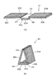
また、本発明の電波吸収体の製造方法では、電波吸収体組立用部材1を折り曲げて組み立てられた電波吸収体を補強するために、補強部材を用いてもよい。図6乃至図8は補強部材を用いる例を示す斜視図である。図6に示される例では、領域2aの端部と領域2cの端部との接合箇所、および領域2aの端部と領域2bの端部との折り曲げ箇所に、楔形の補強部材103を無機接着剤を用いて固着するものである。また、図7に示される例では、断面台形の角柱形状の補強部材104を、領域2aの端部と領域2cの端部との接合箇所、および領域2aの端部と領域2bの端部との折り曲げ箇所に、無機接着剤を用いて固着するものである。さらに、図8に示される例では、楔形状の構造体である電波吸収体101の三角形状の開口部101´に、この開口部と同一形状の補強部材105を嵌合して無機接着剤を用いて固着するものである。
第2の実施形態
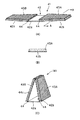
図9は本発明の電波吸収体組立用部材と、これを用いて製造した電波吸収体の他の実施形態を示す斜視図である。図9(A)において、電波吸収体組立用部材11は不燃性の基材12と、この基材12上に固着された電波吸収性の不燃性材13A,13Bとを備えている。基材12は、不燃性材が設けられていない領域12aと、不燃性材13A,13Bが固着されている領域12b,12cとからなり、領域12aと領域12bとの境界、および、領域12aと領域12cとの境界には、それぞれ折り曲げ用の溝部14が設けられている。この基材12は、上記の溝部14において折り曲げることにより、楔形状の構造体を組み立てることができる。尚、基材12や不燃性材13A,13Bの材質、厚み等は、上述のは電波吸収体組立用部材1と同様に設定することができ、ここでの説明は省略する。
【0034】
本実施形態では、上述のような電波吸収体組立用部材11を、基材12の溝部14(電波吸収性の不燃性材13A,13Bが固着されていない部位)で折り曲げて、不燃性材13A,13Bが外側に位置し、基材12の領域12aが底面となるような楔形状の構造体を組み立てる。その後、楔形状の構造体の先端部に位置する基材12の領域12bの端部と領域12cの端部とを接合することにより電波吸収体111(図9(B))を得る。
【0035】
基材12の領域12bの端部と領域12cの端部との接合は、特に制限はなく、上述の図5に示されるようないずれの方法であってもよい。また、例えば、図10に示されるように、予め領域12bの端部と領域12cの端部を斜めに切欠いて当接面12´b,12´cを形成しておき(図10(A))、この当接面12´b,12´cを当接させ(図10(B))、この楔形状の構造体の先端部に係止部材112を無機接着剤で接着(図10(C))することにより接合してもよい。使用する無機接着剤は、上述のような無機接着剤を挙げることができる。また、係止部材112としては、難燃性繊維、ガラス繊維等を無機接着剤を用いて成形したものを使用することができる。
第3の実施形態
図11は本発明の電波吸収体組立用部材と、これを用いて製造した電波吸収体の他の実施形態を示す斜視図である。図11(A)において、電波吸収体組立用部材21は不燃性の基材22と、この基材22の一方の面に固着された電波吸収性の不燃性材23Aと、基材22の他方の面に固着された電波吸収性の不燃性材23B,23Cとを備えている。基材22は、不燃性材22Aが固着されている領域22aと、不燃性材23B,23Cが固着されている領域22b,22cとの境界に、それぞれ折り曲げ用の溝部24が設けられている。この基材22は、上記の溝部24において折り曲げることにより、楔形状の構造体を組み立てることができる。尚、基材22や不燃性材23A,23B,23Cの材質、厚み等は、上述のは電波吸収体組立用部材1と同様に設定することができ、ここでの説明は省略する。
【0036】
本実施形態では、上述のような電波吸収体組立用部材21を、基材22の溝部24(電波吸収性の不燃性材23A,23B,23Cが固着されていない部位)で折り曲げて、不燃性材23B,23Cが外側に位置して不燃性材23Aが内側に位置し、基材22の領域22aが底面となるような楔形状の構造体を組み立てる。その後、楔形状の構造体の先端部に位置する基材22の領域22bの端部と領域22cの端部とを接合することにより電波吸収体121(図11(B))を得る。基材22の領域22bの端部と領域22cの端部との接合は、特に制限はなく、上述の電波吸収体組立用部材11を用いた電波吸収体111の製造と同様に行うことができる。
第4の実施形態
図12は本発明の電波吸収体組立用部材と、これを用いて製造した電波吸収体の他の実施形態を示す斜視図である。図12(A)において、電波吸収体組立用部材31は不燃性の基材32と、この基材32上に固着された三角形状の電波吸収性の不燃性材33A,33B,33C,33Dとを備えている。基材32は、不燃性材33A,33B,33C,33Dが固着されている三角形状の領域32a,32b,32c,32dの各境界に、それぞれ折り曲げ用の溝部34が設けられている。そして、この基材32は、上記の溝部34において折り曲げることにより、四角錐形状の構造体を組み立てることができる。尚、基材32や不燃性材33A,33B,33C,33Dの材質、厚み等は、上述のは電波吸収体組立用部材1と同様に設定することができ、ここでの説明は省略する。
【0037】
本実施形態では、上述のような電波吸収体組立用部材31を、基材32の溝部34(電波吸収性の不燃性材33A,33B,33C,33Dが固着されていない部位)で折り曲げて、不燃性材33A,33B,33C,33Dが外側に位置するような四角錐形状の構造体を組み立てる。その後、四角錐形状の構造体の稜線部に位置する基材32の領域32aの端部と領域32dの端部とを接合することにより電波吸収体131(図12(B))を得る。基材32の領域32aの端部と領域32dの端部との接合は、上述の図5に示されるようないずれの方法であってもよい。
第5の実施形態
図13は本発明の電波吸収体組立用部材と、これを用いて製造した電波吸収体の他の実施形態を示す図である。図13(A)において、電波吸収体組立用部材41は不燃性の基材42と、この基材42上に固着された電波吸収性の不燃性材43A,43Bとを備えている。基材42は、不燃性材が設けられていない領域42aと、不燃性材43A,43Bが固着されている領域42b,42cとからなり、領域42aと領域42bとの境界、および、領域42aと領域42cとの境界には、それぞれ折り曲げ用の溝部44が設けられている。この基材42は、上記の溝部44において折り曲げることにより、楔形状の構造体を組み立てることができる。
【0038】
この電波吸収体組立用部材41は、基本的に上述の電波吸収体組立用部材11と同様であるが、基材42の領域42b,42cの幅が先端部に向けて徐々に狭くなっており、また、不燃性材43A,43Bを保護する目的で、不燃性材43A,43Bの幅よりも基材42の領域42b,42cの幅が大きいような構造となっている点で異なる。図13(B)は図13(A)に示される電波吸収体組立用部材41のA−A線矢視の断面図であり、基材42の領域42bが不燃性材43Aの両側に突出した構造となっている。このような構造では、側面からの衝撃を基材42の突出部分が受けることにより、不燃性材43A,43Bが保護される。
【0039】
尚、基材42や不燃性材43A,43Bの材質、厚み等は、上述のは電波吸収体組立用部材1と同様に設定することができ、ここでの説明は省略する。
【0040】
本実施形態では、上述のような電波吸収体組立用部材41を、基材42の溝部44(電波吸収性の不燃性材43A,43Bが固着されていない部位)で折り曲げて、不燃性材43A,43Bが外側に位置し、基材42の領域42aが底面となるような楔形状の構造体を組み立てる。その後、楔形状の構造体の先端部に位置する基材42の領域42bの端部と領域42cの端部とを接合することにより電波吸収体141(図13(C))を得る。基材42の領域42bの端部と領域42cの端部との接合は、特に制限はなく、上述の電波吸収体組立用部材11を用いた電波吸収体111の製造と同様に行うことができる。製造された電波吸収体141は、底面の幅よりも先端部の幅が狭い楔形状の構造体となっている。
第6の実施形態
図14は本発明の電波吸収体組立用部材と、これを用いて製造した電波吸収体の他の実施形態を示す図である。図14(A)において、電波吸収体組立用部材51は不燃性の基材52と、この基材52上に固着された電波吸収性の不燃性材53A,53Bとを備えている。基材52は、不燃性材が設けられていない領域52aと、不燃性材53A,53Bが固着されている領域52b,52cとからなり、領域52aと領域52bとの境界、および、領域52aと領域52cとの境界には、それぞれ折り曲げ用の溝部54が設けられている。この基材52は、上記の溝部54において折り曲げることにより、楔形状の構造体を組み立てることができる。
【0041】
この電波吸収体組立用部材51は、基本的に上述の電波吸収体組立用部材11と同様であるが、基材52の領域52b,52cの幅が先端部に向けて徐々に狭くなっており、また、不燃性材53A,53Bを保護する目的で、領域52b,52cの3方の端部にそれぞれ保護用フランジ52´b,52´cが折り曲げ可能に設けられている点で異なる。この保護用フランジ52´b,52´cは、図14(B)に示されるように折り曲げて不燃性材53A,53Bの側面に無機接着剤を用いて固着される。図14(C)は図14(B)に示される電波吸収体組立用部材51のB−B線矢視の断面図であり、基材52の領域52b上に固着されている不燃性材53Aの3方の側面は保護用フランジ52´bにより保護された構造となっている。このような構造では、側面からの衝撃を保護用フランジ52´b,52´cが受けることにより、不燃性材53A,53Bが保護される。
【0042】
尚、基材52や不燃性材53A,53Bの材質、厚み等は、上述のは電波吸収体組立用部材1と同様に設定することができ、ここでの説明は省略する。
【0043】
本実施形態では、上述のような電波吸収体組立用部材51を、基材52の溝部54(電波吸収性の不燃性材53A,53Bが固着されていない部位)で折り曲げて、不燃性材53A,53Bが外側に位置し、基材52の領域52aが底面となるような楔形状の構造体を組み立てる。その後、楔形状の構造体の先端部に位置する基材52の領域52bの端部と領域52cの端部とを接合することにより電波吸収体151(図14(D))を得る。基材52の領域52bの端部と領域52cの端部との接合は、特に制限はなく、上述の電波吸収体組立用部材11を用いた電波吸収体111の製造と同様に行うことができる。製造された電波吸収体151は、底面の幅よりも先端部の幅が狭い楔形状の構造体となっている。
第7の実施形態
図15は本発明の電波吸収体組立用部材と、これを用いて製造した電波吸収体の他の実施形態を示す図である。図15(A)において、電波吸収体組立用部材61は不燃性の基材62と、この基材62上に固着された電波吸収性の不燃性材63A,63Bとを備えている。基材62は、不燃性材が設けられていない領域62aと、不燃性材63A,63Bが固着されている領域62b,62cとからなり、領域62aと領域62bとの境界、および、領域62aと領域62cとの境界には、それぞれ折り曲げ用の溝部64が設けられている。この基材62は、上記の溝部64において折り曲げることにより、楔形状の構造体を組み立てることができる。
【0044】
この電波吸収体組立用部材61は、上述の電波吸収体組立用部材51と同様に、不燃性材63A,63Bを保護する目的で、領域62b,62cの3方の端部にそれぞれ保護用フランジ62´b,62´cが折り曲げ可能に設けられているが、この保護用フランジ62´b,62´cが2段階で折り曲げ可能である点で異なる。この保護用フランジ62´b,62´cは、図15(B)に示されるように折り曲げて不燃性材63A,63Bの側面および表面の端部近傍に無機接着剤を用いて固着される。図15(C)は図15(B)に示される電波吸収体組立用部材61のC−C線矢視の断面図であり、基材62の領域62b上に固着されている不燃性材63Aの3方の側面および表面の端部近傍は保護用フランジ62´bにより保護された構造となっている。このような構造では、衝撃を保護用フランジ62´b,62´cが受けることにより、不燃性材63A,63Bが保護され、特に不燃性材63A,63Bの側面と表面との角部が確実に保護される。
【0045】
尚、基材62や不燃性材63A,63Bの材質、厚み等は、上述のは電波吸収体組立用部材1と同様に設定することができ、ここでの説明は省略する。
【0046】
本実施形態では、上述のような電波吸収体組立用部材61を、基材62の溝部64(電波吸収性の不燃性材63A,63Bが固着されていない部位)で折り曲げて、不燃性材63A,63Bが外側に位置し、基材62の領域62aが底面となるような楔形状の構造体を組み立てる。その後、楔形状の構造体の先端部に位置する基材62の領域62bの端部と領域62cの端部とを接合することにより電波吸収体161(図15(D))を得る。基材62の領域62bの端部と領域62cの端部との接合は、特に制限はなく、上述の電波吸収体組立用部材11を用いた電波吸収体111の製造と同様に行うことができる。
第8の実施形態
図16は本発明の電波吸収体組立用部材と、これを用いて製造した電波吸収体の他の実施形態を示す斜視図である。図16(A)において、電波吸収体組立用部材71は不燃性の基材72と、この基材72上に固着された電波吸収性の不燃性材73A,73Bとを備えている。基材72は、不燃性材が設けられていない領域72aと、不燃性材73A,73Bが固着されている領域72b,72cとからなり、領域72aと領域72b、および、領域72aと領域72cとが、それぞれ折り曲げ可能な接合部材76により接合されている。この基材72は、上記の接合部材76を折り曲げることにより、楔形状の構造体を組み立てることができる。
【0047】
図17は、本実施形態の電波吸収体組立用部材71の構造を説明するための図である。図17(A)に示されるように、不燃性の基材72は、長方形状の基材72aと、台形形状の開口を有する回廊形状の基材72b,72cとからなる。回廊形状の基材72b,72cは、周囲にそれぞれ保護用フランジ72´b,72´cが2段階で折り曲げ可能に設けられている。この回廊形状の基材72b,72cに不燃性材73A,73Bを固着し、保護用フランジ72´b,72´cを図17(B)に示されるように折り曲げて不燃性材73A,73Bの側面および表面の端部近傍に無機接着剤を用いて固着する。図17(C)は図17(B)に示されるD−D線矢視の断面図であり、基材72b上に固着されている不燃性材73Aの4方の側面および表面の端部近傍は保護用フランジ72´bにより保護された構造となっている。そして、基材72aに接合部材76を介して基材72b,72cを接合して連結体とすることにより電波吸収体組立用部材71とする。
【0048】
尚、基材72(72a,72b,72c)や不燃性材73A,73Bの材質、厚み等は、上述のは電波吸収体組立用部材1と同様とすることができ、ここでの説明は省略する。
【0049】
本実施形態では、上述のような電波吸収体組立用部材71を、接合部材76が内側となるように折り曲げて、基材72の基材(領域)72aが底面となるような楔形状の構造体を組み立てる。その後、楔形状の構造体の先端部に位置する基材72の基材(領域)72bの端部と基材(領域)72cの端部とを接合することにより電波吸収体171(図16(B))を得る。基材72の基材(領域)72bの端部と基材(領域)72cの端部との接合は、特に制限はなく、上述の電波吸収体組立用部材11を用いた電波吸収体111の製造と同様に行うことができる。
第9の実施形態
上述の電波吸収体組立用部材71は、不燃性材73Aが固着された基材(領域)72bと、不燃性材73Bが固着された基材(領域)72cとが、不燃性材が固着されていない基材72aを介して、折り曲げ可能な接合部材76で接合されたものであるが、本発明の電波吸収体組立用部材は、不燃性材73Aが固着された基材72bと、不燃性材73Bが固着された基材72cとを直接に折り曲げ可能な接合部材76で接合したものであってもよい。図18は、このような本発明の電波吸収体組立用部材と、これを用いて製造した電波吸収体の他の実施形態を示す斜視図である。図18(A)において、電波吸収体組立用部材81は、不燃性材73Aが固着された基材72bと不燃性材73Bが固着された基材72cとを、幅の狭い方の端部において折り曲げ可能な接合部材76aで接合したものを2組作製し、このうちの1組の不燃性材73Aが固着された基材72bと、他の組の不燃性材73Bが固着された基材72cとを、折り曲げ可能な接合部材76bで接合したものである。この接合部材76bで接合する面は、接合部材76aで接合する面と反対側の面である。
【0050】
本実施形態では、上述のような電波吸収体組立用部材81を、接合部材76aが内側となるように折り曲げ、さらに接合部材76bが内側となるように折り曲げて、楔形状の構造体が連立するように組み立て、これにより電波吸収体181(図18(B))を得るものである。
【0051】
【発明の効果】
以上詳述したように、本発明によれば電波吸収体組立用部材は平面形状でかさばることがないので、電波暗室の施工時の搬入作業が極めて容易であり、また、電波吸収体組立用部材に前処理を行うことなく折り曲げて所望の構造体を作製して電波吸収体とするので、作業性が極めて良く、かつ、得られる電波吸収体は不燃性を備えたものとなる。
【図面の簡単な説明】
【図1】本発明の電波吸収体組立用部材と、これを用いて製造した電波吸収体の一実施形態を示す斜視図であり、図1(A)は電波吸収体組立用部材を示し、図1(B)は電波吸収体を示す。
【図2】予め溝部が設けられた不燃性の基材上への不燃性材の固着を説明する部分斜視図であり、図2(A)は固着前の状態を示し、図2(B)は固着された状態を示す。
【図3】本発明の電波吸収体組立用部材を構成する不燃性の基材の他の態様を示す斜視図である。
【図4】不燃性の基材への折り曲げ用の溝部の形成例を示す斜視図である。
【図5】本発明の製造方法における不燃性の基材の端部の接合例を示す図である。
【図6】本発明の製造方法における組み立てられた電波吸収体の補強を説明するための図であり、図6(A)は補強部材の斜視図、図6(B)は補強部材で補強された状態を示す斜視図である。
【図7】本発明の製造方法における組み立てられた電波吸収体の補強を説明するための図であり、図7(A)は補強部材の斜視図、図7(B)は補強部材で補強された状態を示す斜視図である。
【図8】本発明の製造方法における組み立てられた電波吸収体の補強を説明するための図であり、図8(A)は補強部材の斜視図、図8(B)は補強部材で補強された状態を示す斜視図である。
【図9】本発明の電波吸収体組立用部材と、これを用いて製造した電波吸収体の他の実施形態を示す斜視図であり、図9(A)は電波吸収体組立用部材を示し、図9(B)は電波吸収体を示す。
【図10】本発明の製造方法における基材の端部の接合例を示す図である。
【図11】本発明の電波吸収体組立用部材と、これを用いて製造した電波吸収体の他の実施形態を示す斜視図であり、図11(A)は電波吸収体組立用部材を示し、図11(B)は電波吸収体を示す。
【図12】本発明の電波吸収体組立用部材と、これを用いて製造した電波吸収体の他の実施形態を示す斜視図であり、図12(A)は電波吸収体組立用部材を示し、図12(B)は電波吸収体を示す。
【図13】本発明の電波吸収体組立用部材と、これを用いて製造した電波吸収体の他の実施形態を示す図であり、図13(A)は電波吸収体組立用部材を示す斜視図であり、図13(B)は図13(A)のA−A線矢視における断面図であり、図13(C)は電波吸収体を示す斜視図である。
【図14】本発明の電波吸収体組立用部材と、これを用いて製造した電波吸収体の他の実施形態を示す図であり、図14(A)および図14(B)は電波吸収体組立用部材を示す斜視図であり、図14(C)は図14(B)のB−B線矢視における断面図であり、図14(D)は電波吸収体を示す斜視図である。
【図15】本発明の電波吸収体組立用部材と、これを用いて製造した電波吸収体の他の実施形態を示す図であり、図15(A)および図15(B)は電波吸収体組立用部材を示す斜視図であり、図15(C)は図15(B)のC−C線矢視における断面図であり、図15(D)は電波吸収体を示す斜視図である。
【図16】本発明の電波吸収体組立用部材と、これを用いて製造した電波吸収体の他の実施形態を示す斜視図であり、図16(A)は電波吸収体組立用部材を示し、図16(B)は電波吸収体を示す。
【図17】図16に示される電波吸収体組立用部材の構造を説明するための図である。
【図18】本発明の電波吸収体組立用部材と、これを用いて製造した電波吸収体の他の実施形態を示す斜視図であり、図18(A)は電波吸収体組立用部材を示し、図18(B)は電波吸収体を示す。
【符号の説明】
1,11,21,31,41,51,61,71,81…電波吸収体組立用部材
2,12,22,32,42,52,62,72…不燃性の基材
3A,3B,13A,13B,23A,23B,33A,33B,43A,43B,53A,53B,63A,63B…電波吸収性の不燃性材
4,14,24,34,44,54,64…折り曲げ用の溝部
5…開口部
6,76,76a,76b…接合部材
101,111,121,131,141,151,161,171,181…電波吸収体[0001]
BACKGROUND OF THE INVENTION
The present invention relates to an electromagnetic wave absorber used in an anechoic chamber.
[0002]
[Prior art]
In recent years, the use of radio waves has been rapidly expanding, especially in the mobile communication field, toward the realization of a more advanced information society. In addition, various electronic devices have become widespread with the innovative progress of microelectronic technology today. However, with the development of such information communication technology, the influence of unnecessary electromagnetic noise and the like on precision equipment related devices has become a problem.
[0003]
For the measurement of electromagnetic noise, an anechoic chamber (electromagnetic anechoic chamber) that does not reflect electromagnetic waves is usually used, and an electromagnetic wave absorber is disposed on the inner wall of such an anechoic chamber. As a conventional electromagnetic wave absorber used in an electromagnetic wave anechoic chamber, there is an electromagnetic wave absorber made of an organic material such as foamed styrene or foamed styrene or foamed urethane in which carbon black or the like is blended in order to obtain conductivity. The radio wave absorber is used as a three-dimensional structure having a quadrangular pyramid shape, a triangular prism shape, or a wedge shape. An electromagnetic wave absorber having such a three-dimensional structure is obtained by, for example, pre-foaming polystyrene particles before foaming into a spherical shape having a diameter of several millimeters, and coating the surface with a conductive material powder such as carbon black. It is common to produce by secondarily foaming by putting it in a desired mold.
[0004]
In addition, a member to be assembled formed of a thermoplastic synthetic resin having radio wave absorptivity is softened by locally heating a predetermined bent part, and then bent at the bent part to have a desired shape of the radio wave absorber Has been proposed (Japanese Patent No. 2760578).
[0005]
[Problems to be solved by the invention]
However, quadrangular pyramid-shaped, triangular prism-shaped, wedge-shaped electromagnetic wave absorbers manufactured by heating and foaming organic materials such as polystyrene, polystyrene, polyurethane, etc. are bulky at the time of carrying in the installation of the anechoic chamber. However, there is a problem that damage due to contact or the like is likely to occur.
[0006]
Moreover, in the manufacturing method described in Japanese Patent No. 2760578, it is necessary to locally heat and soften a predetermined bent portion, and there is a problem that the work is complicated. Furthermore, since a thermoplastic synthetic resin is used, an anechoic chamber for performing a high power test such as an immunity test has a problem in terms of safety due to incombustibility and fire resistance.
[0007]
The present invention has been made in view of the above circumstances, and can easily manufacture a radio wave absorber of a desired shape that is excellent in workability during construction of an anechoic chamber and has nonflammability. It is an object of the present invention to provide a manufacturing method and a radio wave absorber assembly member that can be used for the manufacturing method.
[0008]
[Means for Solving the Problems]
In order to achieve such an object, the radio wave absorber assembly member of the present invention includes a non-combustible base material capable of assembling a structure having a desired shape, and a radio wave absorptivity fixed to a predetermined portion of the base material. With non-combustible materialThe base material includes a groove for bending at a portion where the incombustible material is not fixed.The configuration is as follows.
[0010]
Further, the radio wave absorber assembly member of the present invention is configured such that the base material is a joined body in which a portion of the base material where the noncombustible material is not fixed is joined by a bendable joining member. .
[0011]
Further, the radio wave absorber assembly member of the present invention is a honeycomb structure in which a non-combustible sheet made from a slurry containing the non-combustible material containing a water-containing inorganic compound and a conductive material is laminated in a honeycomb shape using an inorganic adhesive. It was set as such a structure.
[0012]
Furthermore, the radio wave absorber assembly member of the present invention is configured such that the non-combustible material includes a conductive layer containing a conductive material on the surface.
[0013]
The method for producing a radio wave absorber according to the present invention is a method of processing a non-flammable base material into a shape that allows a structure having a desired shape to be assembled, and fixing the radio wave absorptive non-combustible material to a predetermined portion of the base material. Create body assembly parts,Of the substrateArea where non-combustible material is not fixedA groove for bending is formed in advance, and the grooveThe base material was bent and the end portions of the base material were joined to each other.
[0014]
The method of manufacturing a radio wave absorber according to the present invention includes a radio wave absorptive non-flammable material fixed to a predetermined portion of a non-flammable base material processed into a desired shapeA groove for bending is formed in advance in a portion where the non-combustible material of the base material is not fixed.Are formed, and bonded to each other by a foldable bonding member directly or through a nonflammable base material to which a nonflammable material is not fixed, and a radio wave absorber assembly member is manufactured. Was bent to join the end portions of the substrate.
[0015]
In addition, the method for manufacturing a radio wave absorber according to the present invention is configured such that the radio wave absorber has a quadrangular pyramid shape, a triangular prism shape, or a wedge shape.
[0017]
In the present invention, the radio wave absorber assembly member is flat and easy to handle without being bulky, and a desired structure is produced by bending the non-combustible base material of the radio wave absorber assembly member. Or by bending a radio wave absorber assembly member with a joining member to produce a desired structure, a radio wave absorber having a radio wave absorptive incombustible material fixed to a predetermined portion of the structure. Obtainable.
[0018]
DETAILED DESCRIPTION OF THE INVENTION
Embodiments of the present invention will be described below.
First embodiment
FIG. 1 is a perspective view showing a radio wave absorber assembling member of the present invention and a radio wave absorber manufactured using the same. In FIG. 1A, a radio wave absorber assembling member 1 includes a
[0019]
The
[0020]
Examples of the
[0021]
Moreover, in this invention, you may provide an opening part in the range in which the mechanical strength of the
[0022]
The formation of the bending
[0023]
The
[0024]
The radio wave absorptive
[0025]
As the conductive material, carbon black, graphite, carbon fiber, or the like can be used. As the closed-cell inorganic particles, Shirasu balloons, silica balloons, glass beads, perlite, alumina silica balloons, and the like can be used. As the inorganic adhesive, an adhesive that hardens by a hydration reaction such as Portland cement or gypsum, or an inorganic adhesive such as a phosphate, silica sol, or a water glass composition can be used. A water glass composition having high binding properties can be preferably used. Water glass is an aqueous solution mainly composed of alkali metal silicate, and sodium silicate is particularly preferable because it is inexpensive and readily available as a JIS standard product. Alternatively, a sodium silicate water glass may be mixed with a lithium silicate water glass.
[0026]
The honeycomb structure as the
[0027]
The thickness of the
[0028]
In the present invention, a conductive layer containing a conductive material may be provided on the surfaces of the
[0029]
In the present invention, an inorganic film made of water glass or the like may be further formed on the conductive layer as described above. By providing this inorganic coating, the tensile strength and compressive strength of the non-combustible material, particularly the honeycomb structure, can be further increased, and the stretched state of the honeycomb structure can be more stably maintained.
[0030]
In the method for manufacturing a radio wave absorber according to the present invention, the radio wave absorber assembling member 1 as described above is bent at a
[0031]
Regarding the folding of the
[0032]
The joining of the end of the region 2a of the
[0033]
In the method for manufacturing a radio wave absorber according to the present invention, a reinforcing member may be used to reinforce the radio wave absorber assembled by bending the radio wave absorber assembling member 1. 6 to 8 are perspective views showing an example in which a reinforcing member is used. In the example shown in FIG. 6, a wedge-shaped reinforcing
Second embodiment
FIG. 9 is a perspective view showing a radio wave absorber assembling member of the present invention and another embodiment of a radio wave absorber manufactured using the same. In FIG. 9A, the radio wave
[0034]
In the present embodiment, the radio wave
[0035]
The joining of the end of the
Third embodiment
FIG. 11 is a perspective view showing another embodiment of a radio wave absorber assembly member of the present invention and a radio wave absorber manufactured using the same. In FIG. 11A, the radio wave
[0036]
In the present embodiment, the radio wave
Fourth embodiment
FIG. 12 is a perspective view showing a radio wave absorber assembling member of the present invention and another embodiment of the radio wave absorber manufactured using the same. In FIG. 12A, a radio wave
[0037]
In the present embodiment, the radio wave
Fifth embodiment
FIG. 13 is a diagram showing a radio wave absorber assembly member of the present invention and another embodiment of a radio wave absorber manufactured using the same. In FIG. 13A, the radio wave
[0038]
The radio wave
[0039]
The material, thickness, and the like of the
[0040]
In the present embodiment, the radio wave
Sixth embodiment
FIG. 14 is a view showing a radio wave absorber assembly member of the present invention and another embodiment of a radio wave absorber manufactured using the same. 14A, the radio wave
[0041]
The radio wave
[0042]
The material, thickness, and the like of the
[0043]
In the present embodiment, the radio wave
Seventh embodiment
FIG. 15 is a view showing a radio wave absorber assembly member of the present invention and another embodiment of a radio wave absorber manufactured using the same. In FIG. 15A, the radio wave
[0044]
Similarly to the above-described radio wave
[0045]
Note that the materials, thicknesses, and the like of the
[0046]
In the present embodiment, the radio wave
Eighth embodiment
FIG. 16 is a perspective view showing a radio wave absorber assembling member of the present invention and another embodiment of the radio wave absorber manufactured using the same. In FIG. 16A, the radio wave absorber assembling member 71 includes a
[0047]
FIG. 17 is a view for explaining the structure of the radio wave absorber assembly member 71 of the present embodiment. As shown in FIG. 17A, the
[0048]
The materials, thicknesses, and the like of the base material 72 (72a, 72b, 72c) and the
[0049]
In this embodiment, the electromagnetic wave absorber assembling member 71 as described above is bent so that the joining
Ninth embodiment
In the radio wave absorber assembling member 71, the base material (region) 72b to which the
[0050]
In the present embodiment, the radio wave
[0051]
【The invention's effect】
As described above in detail, according to the present invention, the electromagnetic wave absorber assembling member is flat and does not become bulky, so that it is very easy to carry in at the time of construction of the anechoic chamber, and the electromagnetic wave absorber assembly member In addition, since a desired structure is produced by bending without performing pretreatment, the workability is very good, and the obtained wave absorber has nonflammability.
[Brief description of the drawings]
FIG. 1 is a perspective view showing an embodiment of a radio wave absorber assembly member of the present invention and a radio wave absorber manufactured using the same; FIG. 1 (A) shows a radio wave absorber assembly member; FIG. 1B shows a radio wave absorber.
FIG. 2 is a partial perspective view illustrating fixing of a non-combustible material on a non-combustible base material provided with a groove in advance, and FIG. 2 (A) shows a state before fixing, and FIG. Indicates a fixed state.
FIG. 3 is a perspective view showing another embodiment of the non-combustible base material constituting the radio wave absorber assembly member of the present invention.
FIG. 4 is a perspective view showing an example of forming a groove for bending on a nonflammable substrate.
FIG. 5 is a view showing an example of joining of end portions of a nonflammable substrate in the production method of the present invention.
6A and 6B are views for explaining reinforcement of the assembled radio wave absorber in the manufacturing method of the present invention, FIG. 6A is a perspective view of the reinforcing member, and FIG. 6B is reinforced by the reinforcing member. FIG.
7A and 7B are diagrams for explaining reinforcement of the assembled radio wave absorber in the manufacturing method of the present invention, FIG. 7A is a perspective view of the reinforcing member, and FIG. 7B is reinforced by the reinforcing member. FIG.
8A and 8B are views for explaining reinforcement of the assembled radio wave absorber in the manufacturing method of the present invention. FIG. 8A is a perspective view of the reinforcing member, and FIG. 8B is reinforced by the reinforcing member. FIG.
FIG. 9 is a perspective view showing another embodiment of a radio wave absorber assembly member of the present invention and a radio wave absorber manufactured using the same, and FIG. 9 (A) shows the radio wave absorber assembly member. FIG. 9B shows a radio wave absorber.
FIG. 10 is a view showing an example of joining of end portions of base materials in the production method of the present invention.
FIG. 11 is a perspective view showing another embodiment of a radio wave absorber assembly member of the present invention and a radio wave absorber manufactured using the same, and FIG. 11 (A) shows the radio wave absorber assembly member. FIG. 11B shows a radio wave absorber.
FIG. 12 is a perspective view showing another embodiment of the radio wave absorber assembly member of the present invention and a radio wave absorber manufactured using the same, and FIG. 12 (A) shows the radio wave absorber assembly member. FIG. 12B shows a radio wave absorber.
FIG. 13 is a view showing another embodiment of the radio wave absorber assembling member of the present invention and a radio wave absorber manufactured using the same, and FIG. 13 (A) is a perspective view showing the radio wave absorber assembling member. FIG. 13B is a cross-sectional view taken along line AA in FIG. 13A, and FIG. 13C is a perspective view showing a radio wave absorber.
FIG. 14 is a view showing another embodiment of the radio wave absorber assembly member of the present invention and a radio wave absorber manufactured using the member, and FIGS. 14 (A) and 14 (B) are radio wave absorbers. It is a perspective view which shows the member for an assembly, FIG.14 (C) is sectional drawing in the BB arrow of FIG.14 (B), FIG.14 (D) is a perspective view which shows an electromagnetic wave absorber.
FIGS. 15A and 15B are diagrams showing another embodiment of a radio wave absorber assembling member of the present invention and a radio wave absorber manufactured using the member, and FIGS. 15A and 15B show the radio wave absorber. It is a perspective view which shows the member for an assembly, FIG.15 (C) is sectional drawing in CC arrow of FIG.15 (B), FIG.15 (D) is a perspective view which shows an electromagnetic wave absorber.
FIG. 16 is a perspective view showing another embodiment of a radio wave absorber assembly member of the present invention and a radio wave absorber manufactured using the same, and FIG. 16 (A) shows the radio wave absorber assembly member. FIG. 16B shows a radio wave absorber.
FIG. 17 is a view for explaining the structure of the radio wave absorber assembly member shown in FIG. 16;
FIG. 18 is a perspective view showing another embodiment of the radio wave absorber assembly member of the present invention and a radio wave absorber manufactured using the same, and FIG. 18 (A) shows the radio wave absorber assembly member. FIG. 18B shows a radio wave absorber.
[Explanation of symbols]
1, 11, 21, 31, 41, 51, 61, 71, 81...
2, 12, 22, 32, 42, 52, 62, 72 ... non-flammable substrate
3A, 3B, 13A, 13B, 23A, 23B, 33A, 33B, 43A, 43B, 53A, 53B, 63A, 63B ... non-combustible material that absorbs radio waves
4, 14, 24, 34, 44, 54, 64 ... grooves for bending
5 ... Opening
6, 76, 76a, 76b ... Joining member
101, 111, 121, 131, 141, 151, 161, 171, 181, ... wave absorber
Claims (7)
Priority Applications (7)
| Application Number | Priority Date | Filing Date | Title |
|---|---|---|---|
| JP29762498A JP4299387B2 (en) | 1998-10-05 | 1998-10-05 | Radio wave absorber assembly member and radio wave absorber manufacturing method |
| KR1019990041888A KR100666761B1 (en) | 1998-10-05 | 1999-09-30 | Member for assembling radio wave absorber and method of producing radio wave absorber |
| TW088117123A TWI246396B (en) | 1998-10-05 | 1999-10-05 | Method of producing radio wave absorber |
| EP99119700A EP0993071B1 (en) | 1998-10-05 | 1999-10-05 | Member for assembling radio wave absorber and method of producing radio wave absorber |
| TW091205121U TW540998U (en) | 1998-10-05 | 1999-10-05 | Member for assembling radio wave absorber |
| DE69936752T DE69936752T2 (en) | 1998-10-05 | 1999-10-05 | Apparatus for composing a radio wave absorber and its manufacturing method |
| US09/412,780 US6613975B1 (en) | 1998-10-05 | 1999-10-05 | Member for assembling radio wave absorber and method of producing radio wave absorber |
Applications Claiming Priority (1)
| Application Number | Priority Date | Filing Date | Title |
|---|---|---|---|
| JP29762498A JP4299387B2 (en) | 1998-10-05 | 1998-10-05 | Radio wave absorber assembly member and radio wave absorber manufacturing method |
Publications (3)
| Publication Number | Publication Date |
|---|---|
| JP2000114774A JP2000114774A (en) | 2000-04-21 |
| JP2000114774A5 JP2000114774A5 (en) | 2005-10-27 |
| JP4299387B2 true JP4299387B2 (en) | 2009-07-22 |
Family
ID=17848983
Family Applications (1)
| Application Number | Title | Priority Date | Filing Date |
|---|---|---|---|
| JP29762498A Expired - Fee Related JP4299387B2 (en) | 1998-10-05 | 1998-10-05 | Radio wave absorber assembly member and radio wave absorber manufacturing method |
Country Status (6)
| Country | Link |
|---|---|
| US (1) | US6613975B1 (en) |
| EP (1) | EP0993071B1 (en) |
| JP (1) | JP4299387B2 (en) |
| KR (1) | KR100666761B1 (en) |
| DE (1) | DE69936752T2 (en) |
| TW (2) | TWI246396B (en) |
Families Citing this family (13)
| Publication number | Priority date | Publication date | Assignee | Title |
|---|---|---|---|---|
| JP4377467B2 (en) * | 1999-01-21 | 2009-12-02 | Tdk株式会社 | Radio wave absorber assembly member and radio wave absorber using the same |
| JP2002094282A (en) * | 2000-09-11 | 2002-03-29 | Ii & C Eng Kk | Radio wave absorbent and its manufacturing method |
| JP2005197307A (en) * | 2003-12-26 | 2005-07-21 | Nippon Muki Co Ltd | Solid electromagnetic wave absorption material |
| US20060007034A1 (en) * | 2004-07-07 | 2006-01-12 | Wen-Jang Yen | Composite radar absorption structure with a thin shell type and method for manufacturing the same |
| KR100660356B1 (en) * | 2004-10-19 | 2006-12-21 | 이정수 | reinforcing strip for supporting reinforced earth wall and its placement method |
| DE102007058480A1 (en) * | 2007-12-04 | 2009-06-10 | Frankonia Handels- und Vertriebsgesellschaft für chemisch- und elektrotechnische Produkte mbH | Absorber for wide-band absorption of electromagnetic waves, and for use as hybrid absorber, has electrically conductive absorber body, and is tapered upwards from base area, where absorber body is made of calcium silicate mixture |
| JP5360552B2 (en) * | 2009-02-25 | 2013-12-04 | 北川工業株式会社 | gasket |
| GB2484942A (en) * | 2010-10-26 | 2012-05-02 | Vestas Wind Sys As | Flexible ground plane and core structure for an RF signal absorbing arrangement |
| KR101698110B1 (en) * | 2016-10-21 | 2017-01-19 | 국방과학연구소 | Electromagnetic Absorber attached to object |
| CN109752599A (en) * | 2017-11-08 | 2019-05-14 | 伟睿科技(深圳)有限公司 | The shielding castle of upper and lower open and close type |
| CN110398721B (en) * | 2018-04-25 | 2022-07-15 | 成都飞机工业(集团)有限责任公司 | Radar wave-absorbing material shielding screen forming method |
| JP2020167349A (en) * | 2019-03-29 | 2020-10-08 | 日東電工株式会社 | Cover, covered component and radar device |
| RU199870U1 (en) * | 2020-06-18 | 2020-09-24 | Елена Николаевна Хандогина | Electromagnetic absorption device |
Family Cites Families (15)
| Publication number | Priority date | Publication date | Assignee | Title |
|---|---|---|---|---|
| JPS63252500A (en) | 1987-04-09 | 1988-10-19 | セイコーインスツルメンツ株式会社 | Isotropic electromagnetic wave absorber |
| JPH0225277A (en) | 1988-07-13 | 1990-01-26 | Fujitsu Ltd | Method of assembling cooler |
| JP2760578B2 (en) * | 1989-07-03 | 1998-06-04 | アクゾ・カシマ株式会社 | Manufacturing method of radio wave absorber |
| JP2743227B2 (en) | 1992-02-26 | 1998-04-22 | パラマウント硝子工業株式会社 | Heat-resistant and non-flammable radio wave absorber |
| IT1254362B (en) * | 1992-05-12 | 1995-09-14 | STRUCTURAL RESONANCE ABSORPTION DEVICE FOR THE REDUCTION OF RADAR REFLECTIONS. | |
| DE4405847C2 (en) * | 1994-02-03 | 1996-02-08 | Huelsta Werke Huels Kg | Folding strip with rounded bending edge |
| JP3394848B2 (en) | 1994-06-23 | 2003-04-07 | 株式会社竹中工務店 | Radio wave absorber member, radio wave absorber, and method of manufacturing radio wave absorber member |
| EP0689262B1 (en) * | 1994-06-23 | 1999-12-01 | Takenaka Corporation | Wave absorber composition, radio wave absorber member, radio wave absorber and method for producing wave absorber member |
| JPH0883992A (en) * | 1994-09-12 | 1996-03-26 | Natl Space Dev Agency Japan<Nasda> | Radio-wave absorber |
| US5594218A (en) * | 1995-01-04 | 1997-01-14 | Northrop Grumman Corporation | Anechoic chamber absorber and method |
| JPH1051180A (en) | 1996-04-05 | 1998-02-20 | Nisshinbo Ind Inc | Radio-wave absorber |
| JPH09307268A (en) * | 1996-05-13 | 1997-11-28 | Tohoku Kako Kk | Radio wave absorbing material |
| US6344255B1 (en) * | 1998-08-28 | 2002-02-05 | Tdk Corporation | Radio wave transmitting material |
| JP2000077883A (en) * | 1998-08-28 | 2000-03-14 | Tdk Corp | Incombustible honeycomb radio-absorptive material and radio-wave absorber using the same |
| JP4377467B2 (en) * | 1999-01-21 | 2009-12-02 | Tdk株式会社 | Radio wave absorber assembly member and radio wave absorber using the same |
-
1998
- 1998-10-05 JP JP29762498A patent/JP4299387B2/en not_active Expired - Fee Related
-
1999
- 1999-09-30 KR KR1019990041888A patent/KR100666761B1/en not_active IP Right Cessation
- 1999-10-05 TW TW088117123A patent/TWI246396B/en not_active IP Right Cessation
- 1999-10-05 DE DE69936752T patent/DE69936752T2/en not_active Expired - Lifetime
- 1999-10-05 EP EP99119700A patent/EP0993071B1/en not_active Expired - Lifetime
- 1999-10-05 TW TW091205121U patent/TW540998U/en not_active IP Right Cessation
- 1999-10-05 US US09/412,780 patent/US6613975B1/en not_active Expired - Fee Related
Also Published As
| Publication number | Publication date |
|---|---|
| EP0993071A3 (en) | 2000-11-29 |
| DE69936752D1 (en) | 2007-09-20 |
| EP0993071A2 (en) | 2000-04-12 |
| DE69936752T2 (en) | 2007-12-06 |
| KR20000028734A (en) | 2000-05-25 |
| EP0993071B1 (en) | 2007-08-08 |
| US6613975B1 (en) | 2003-09-02 |
| TWI246396B (en) | 2005-12-21 |
| JP2000114774A (en) | 2000-04-21 |
| KR100666761B1 (en) | 2007-01-09 |
| TW540998U (en) | 2003-07-01 |
Similar Documents
| Publication | Publication Date | Title |
|---|---|---|
| JP4299387B2 (en) | Radio wave absorber assembly member and radio wave absorber manufacturing method | |
| EP0982801B1 (en) | Incombustible honeycomb radio absorptive material and radio absorber using the same | |
| JP4377467B2 (en) | Radio wave absorber assembly member and radio wave absorber using the same | |
| EP0986294A2 (en) | Electric wave absorber | |
| JPH01306236A (en) | Element for self-supporting structure | |
| KR100447887B1 (en) | Radio Wave Transmitting Material | |
| JP2000082893A (en) | Radio wave absorbing body | |
| JPH05222784A (en) | Heat-sound-fire preventing panel | |
| JPH0471802A (en) | Thermal insulating plate serving as framework | |
| JPS6316730Y2 (en) | ||
| JPH0688374B2 (en) | Composite plywood | |
| JPS5935728Y2 (en) | architectural composite board | |
| JPH01262126A (en) | Fire-retardant expanded resin laminated board | |
| KR100363336B1 (en) | A panel and manufacture method of panel for construction | |
| JP2000082892A (en) | Radio wave absorbing body | |
| JPS6035698Y2 (en) | Fireproof insulation construction board | |
| JPS6127410Y2 (en) | ||
| JPH06299618A (en) | Panel also used for form | |
| JPS6140825Y2 (en) | ||
| JPS647564B2 (en) | ||
| JP2001317136A (en) | Joint material for electromagnetic wave shield | |
| JPH0978798A (en) | Panel for building | |
| JPH07357B2 (en) | Non-combustible honeycomb structure material and non-combustible board | |
| KR20100038682A (en) | Noise reduction member having sandwich structure consisting of sound absorbing porous concrete and polyurethane | |
| JPS6349276A (en) | Method for constituting adhering and coating stock for slip carrier having various function characteristics including sound absorptivity or shieldability of middle and low frequency range and electromagnetic wave shieldability and for constituting thin film matching ratio lamination function method for of blanket carrier and for constituting unit type lamination function thereof |
Legal Events
| Date | Code | Title | Description |
|---|---|---|---|
| A521 | Request for written amendment filed |
Free format text: JAPANESE INTERMEDIATE CODE: A523 Effective date: 20050728 |
|
| A621 | Written request for application examination |
Free format text: JAPANESE INTERMEDIATE CODE: A621 Effective date: 20050728 |
|
| A131 | Notification of reasons for refusal |
Free format text: JAPANESE INTERMEDIATE CODE: A131 Effective date: 20080805 |
|
| A521 | Request for written amendment filed |
Free format text: JAPANESE INTERMEDIATE CODE: A523 Effective date: 20081003 |
|
| TRDD | Decision of grant or rejection written | ||
| A01 | Written decision to grant a patent or to grant a registration (utility model) |
Free format text: JAPANESE INTERMEDIATE CODE: A01 Effective date: 20090407 |
|
| A01 | Written decision to grant a patent or to grant a registration (utility model) |
Free format text: JAPANESE INTERMEDIATE CODE: A01 |
|
| A61 | First payment of annual fees (during grant procedure) |
Free format text: JAPANESE INTERMEDIATE CODE: A61 Effective date: 20090417 |
|
| R150 | Certificate of patent or registration of utility model |
Free format text: JAPANESE INTERMEDIATE CODE: R150 |
|
| FPAY | Renewal fee payment (event date is renewal date of database) |
Free format text: PAYMENT UNTIL: 20120424 Year of fee payment: 3 |
|
| FPAY | Renewal fee payment (event date is renewal date of database) |
Free format text: PAYMENT UNTIL: 20120424 Year of fee payment: 3 |
|
| FPAY | Renewal fee payment (event date is renewal date of database) |
Free format text: PAYMENT UNTIL: 20130424 Year of fee payment: 4 |
|
| FPAY | Renewal fee payment (event date is renewal date of database) |
Free format text: PAYMENT UNTIL: 20130424 Year of fee payment: 4 |
|
| FPAY | Renewal fee payment (event date is renewal date of database) |
Free format text: PAYMENT UNTIL: 20140424 Year of fee payment: 5 |
|
| LAPS | Cancellation because of no payment of annual fees |