JP4283087B2 - 光電変換素子 - Google Patents
光電変換素子 Download PDFInfo
- Publication number
- JP4283087B2 JP4283087B2 JP2003370850A JP2003370850A JP4283087B2 JP 4283087 B2 JP4283087 B2 JP 4283087B2 JP 2003370850 A JP2003370850 A JP 2003370850A JP 2003370850 A JP2003370850 A JP 2003370850A JP 4283087 B2 JP4283087 B2 JP 4283087B2
- Authority
- JP
- Japan
- Prior art keywords
- electrode
- photoelectric conversion
- metal
- solder
- conversion element
- Prior art date
- Legal status (The legal status is an assumption and is not a legal conclusion. Google has not performed a legal analysis and makes no representation as to the accuracy of the status listed.)
- Expired - Fee Related
Links
- 238000006243 chemical reaction Methods 0.000 title claims abstract description 25
- 239000000758 substrate Substances 0.000 claims abstract description 44
- 229910000679 solder Inorganic materials 0.000 claims abstract description 41
- 239000004065 semiconductor Substances 0.000 claims abstract description 39
- 239000011521 glass Substances 0.000 claims abstract description 38
- 239000007769 metal material Substances 0.000 claims abstract description 12
- 239000004020 conductor Substances 0.000 claims abstract description 5
- 239000010410 layer Substances 0.000 claims description 71
- XUIMIQQOPSSXEZ-UHFFFAOYSA-N Silicon Chemical compound [Si] XUIMIQQOPSSXEZ-UHFFFAOYSA-N 0.000 claims description 31
- 229910052710 silicon Inorganic materials 0.000 claims description 31
- 239000010703 silicon Substances 0.000 claims description 31
- 239000000956 alloy Substances 0.000 claims description 26
- 229910045601 alloy Inorganic materials 0.000 claims description 24
- 239000002356 single layer Substances 0.000 claims description 8
- 229910052759 nickel Inorganic materials 0.000 claims description 7
- 229910052697 platinum Inorganic materials 0.000 claims description 6
- 229910052763 palladium Inorganic materials 0.000 claims description 5
- 229910052802 copper Inorganic materials 0.000 claims description 4
- 229910052709 silver Inorganic materials 0.000 claims description 4
- 229910006404 SnO 2 Inorganic materials 0.000 claims description 2
- 229910052718 tin Inorganic materials 0.000 claims description 2
- 229910052725 zinc Inorganic materials 0.000 claims description 2
- 238000000034 method Methods 0.000 abstract description 37
- 238000004519 manufacturing process Methods 0.000 abstract description 12
- 229910052751 metal Inorganic materials 0.000 description 76
- 239000002184 metal Substances 0.000 description 76
- 239000010408 film Substances 0.000 description 46
- 229920005989 resin Polymers 0.000 description 26
- 239000011347 resin Substances 0.000 description 26
- 230000008569 process Effects 0.000 description 17
- 239000000463 material Substances 0.000 description 16
- 229910021417 amorphous silicon Inorganic materials 0.000 description 14
- 238000004544 sputter deposition Methods 0.000 description 14
- 230000015572 biosynthetic process Effects 0.000 description 10
- 238000007650 screen-printing Methods 0.000 description 9
- 150000002739 metals Chemical class 0.000 description 7
- 230000035945 sensitivity Effects 0.000 description 7
- 239000012071 phase Substances 0.000 description 6
- 238000007789 sealing Methods 0.000 description 6
- 230000000873 masking effect Effects 0.000 description 5
- 230000007246 mechanism Effects 0.000 description 5
- 238000000605 extraction Methods 0.000 description 4
- 230000003287 optical effect Effects 0.000 description 4
- 230000003647 oxidation Effects 0.000 description 4
- 238000007254 oxidation reaction Methods 0.000 description 4
- 238000005268 plasma chemical vapour deposition Methods 0.000 description 4
- 239000010409 thin film Substances 0.000 description 4
- 239000012808 vapor phase Substances 0.000 description 4
- 229920002799 BoPET Polymers 0.000 description 3
- 238000005452 bending Methods 0.000 description 3
- 239000003990 capacitor Substances 0.000 description 3
- 238000010586 diagram Methods 0.000 description 3
- 230000000694 effects Effects 0.000 description 3
- 229910052737 gold Inorganic materials 0.000 description 3
- 229910021421 monocrystalline silicon Inorganic materials 0.000 description 3
- 238000007747 plating Methods 0.000 description 3
- 230000000007 visual effect Effects 0.000 description 3
- 238000004804 winding Methods 0.000 description 3
- 206010034972 Photosensitivity reaction Diseases 0.000 description 2
- 230000008901 benefit Effects 0.000 description 2
- 230000008859 change Effects 0.000 description 2
- 238000012790 confirmation Methods 0.000 description 2
- 238000000151 deposition Methods 0.000 description 2
- 238000007599 discharging Methods 0.000 description 2
- 230000006872 improvement Effects 0.000 description 2
- 238000003475 lamination Methods 0.000 description 2
- 239000000203 mixture Substances 0.000 description 2
- 230000010355 oscillation Effects 0.000 description 2
- 230000036211 photosensitivity Effects 0.000 description 2
- 150000003376 silicon Chemical class 0.000 description 2
- 229910052719 titanium Inorganic materials 0.000 description 2
- 238000004506 ultrasonic cleaning Methods 0.000 description 2
- 238000007740 vapor deposition Methods 0.000 description 2
- 230000009471 action Effects 0.000 description 1
- 229910052782 aluminium Inorganic materials 0.000 description 1
- 239000003985 ceramic capacitor Substances 0.000 description 1
- 229910052804 chromium Inorganic materials 0.000 description 1
- 239000006071 cream Substances 0.000 description 1
- 239000013078 crystal Substances 0.000 description 1
- 238000005520 cutting process Methods 0.000 description 1
- 230000007547 defect Effects 0.000 description 1
- 238000001514 detection method Methods 0.000 description 1
- 239000007772 electrode material Substances 0.000 description 1
- 230000003628 erosive effect Effects 0.000 description 1
- 238000005530 etching Methods 0.000 description 1
- 230000010354 integration Effects 0.000 description 1
- 239000011229 interlayer Substances 0.000 description 1
- 238000005304 joining Methods 0.000 description 1
- 230000031700 light absorption Effects 0.000 description 1
- 239000007791 liquid phase Substances 0.000 description 1
- 229910052750 molybdenum Inorganic materials 0.000 description 1
- 238000004806 packaging method and process Methods 0.000 description 1
- 238000000206 photolithography Methods 0.000 description 1
- 229920000728 polyester Polymers 0.000 description 1
- 238000007639 printing Methods 0.000 description 1
- 238000010298 pulverizing process Methods 0.000 description 1
- 238000005477 sputtering target Methods 0.000 description 1
- 239000000126 substance Substances 0.000 description 1
- 229910052715 tantalum Inorganic materials 0.000 description 1
- 229920001187 thermosetting polymer Polymers 0.000 description 1
- 229910052721 tungsten Inorganic materials 0.000 description 1
Images


Classifications
-
- Y—GENERAL TAGGING OF NEW TECHNOLOGICAL DEVELOPMENTS; GENERAL TAGGING OF CROSS-SECTIONAL TECHNOLOGIES SPANNING OVER SEVERAL SECTIONS OF THE IPC; TECHNICAL SUBJECTS COVERED BY FORMER USPC CROSS-REFERENCE ART COLLECTIONS [XRACs] AND DIGESTS
- Y02—TECHNOLOGIES OR APPLICATIONS FOR MITIGATION OR ADAPTATION AGAINST CLIMATE CHANGE
- Y02E—REDUCTION OF GREENHOUSE GAS [GHG] EMISSIONS, RELATED TO ENERGY GENERATION, TRANSMISSION OR DISTRIBUTION
- Y02E10/00—Energy generation through renewable energy sources
- Y02E10/50—Photovoltaic [PV] energy
Landscapes
- Photovoltaic Devices (AREA)
- Light Receiving Elements (AREA)
Description
また、素子側面に半田付けができることにより素子の傾きが自己矯正でき、従来の下面電極構造で問題となっていた受光量の変化による出力特性のばらつきを抑えることが可能となる。更に下面、側面の電極構造を問わず、メタルマスクやリフトオフ法を用いた金属電極の形成方法により、従来の印刷工程数を半減以下にすることができ、大幅な工程数削減が可能となる。
この様に実装された素子は個々の材料の強度および密着性が大変優れており、非常に強い実装強度を示すようになる。
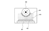
1.0PaのAr雰囲気下でRF出力1.0kWの放電にて1.5μmの成膜を行った。ITO、Ni両者とも円柱状の成膜治具を回転させて成膜を行い、ガラス端面の膜厚制御を行った。
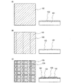
102、302、502 非晶質シリコン半導体層
103、303 コンタクトホール
104、304、503 金属電極(正極)
105、305、504 金属電極(負極)
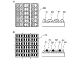
201、306、505 封止樹脂
202 予備半田
401 スパッタリング電極(カソード)
402 スパッタリングターゲット
403 放電空間
404 短冊状切断基板
405 スパッタリング電極(アノード)
506、702、803 半田
507、703 金属ランド
508、704、802 回路基板
602 透明導電膜
603 p型非晶質シリコン半導体層
604 i型非晶質シリコン半導体層
605 n型非晶質半導体層
606 導電性樹脂(一次電極)
607 封止樹脂
608 導電性樹脂(二次電極)
609 受光面
701、801 下面電極素子(可視光センサ)
705 側面電極素子(チップコンデンサ)
706 側面電極
804 破断面
805 対垂直入射光受光領域(傾き無し)
806 対垂直入射光受光領域(傾き有り)
Claims (9)
- ガラス基板上に、p型シリコン膜と、i型シリコン膜と、n型シリコン膜とがこの順に積層された半導体層を有し、
前記n型シリコン膜は、前記n型シリコン膜上に形成された第1の電極と電気的に接続され、
前記p型シリコン膜は、前記p型シリコン膜と前記i型シリコン膜と前記n型シリコン膜とに形成された開口部において、第2の電極と電気的に接続され、
前記開口部の側面はテーパー状であることを特徴とする光電変換素子。 - 請求項1において、
前記開口部は複数設けられていることを特徴とする光電変換素子。 - 請求項1または請求項2において、
前記第1の電極と前記第2の電極は同時に形成されることを特徴とする光電変換素子。 - 請求項1乃至請求項3のいずれか一において、
前記第1の電極と前記第2の電極は、前記半導体層と接触する内層部が酸化物系導電材料から成り、外層部が半田と合金形成が可能な金属材料で形成されている積層構造を有することを特徴とする光電変換素子。 - 請求項1乃至請求項3のいずれか一において、
前記第1の電極と前記第2の電極は、前記半導体層と接触する内層部が酸化物系導電材料から成り、外層部が半田と合金形成が可能な金属材料で形成されている積層構造を有し、前記ガラス基板の端面まで連続して形成されていることを特徴とする光電変換素子。 - 請求項1乃至請求項3のいずれか一において、
前記第1の電極と前記第2の電極は、前記半導体層とオーム接触を示し、かつ半田と合金形成が可能な金属材料の単層構造で形成されていることを特徴とする光電変換素子。 - 請求項4または請求項5において、
前記外層部がNi、Cu、Zn、Pd、Ag、Sn、Pt、Auから選ばれた一元素、又は前記元素を50%以上含む合金材料で形成されており、膜厚が0.1μm〜50μmの範囲であることを特徴とする光電変換素子。 - 請求項4、請求項5または請求項7において、
前記内層部がITO、SnO2、ZnOから選ばれた一種又は複数種の酸化物系導電材料で形成されていることを特徴とする光電変換素子。 - 請求項6において、
前記第1の電極と前記第2の電極がNi、Pd、Pt、Auから選ばれた一元素、又は前記元素を50%以上含む合金材料で形成されており、膜厚が0.1μm〜50μmの範囲であることを特徴とする光電変換素子。
Priority Applications (1)
| Application Number | Priority Date | Filing Date | Title |
|---|---|---|---|
| JP2003370850A JP4283087B2 (ja) | 2002-10-30 | 2003-10-30 | 光電変換素子 |
Applications Claiming Priority (2)
| Application Number | Priority Date | Filing Date | Title |
|---|---|---|---|
| JP2002316119 | 2002-10-30 | ||
| JP2003370850A JP4283087B2 (ja) | 2002-10-30 | 2003-10-30 | 光電変換素子 |
Publications (3)
| Publication Number | Publication Date |
|---|---|
| JP2004172603A JP2004172603A (ja) | 2004-06-17 |
| JP2004172603A5 JP2004172603A5 (ja) | 2006-10-26 |
| JP4283087B2 true JP4283087B2 (ja) | 2009-06-24 |
Family
ID=32715814
Family Applications (1)
| Application Number | Title | Priority Date | Filing Date |
|---|---|---|---|
| JP2003370850A Expired - Fee Related JP4283087B2 (ja) | 2002-10-30 | 2003-10-30 | 光電変換素子 |
Country Status (1)
| Country | Link |
|---|---|
| JP (1) | JP4283087B2 (ja) |
Families Citing this family (6)
| Publication number | Priority date | Publication date | Assignee | Title |
|---|---|---|---|---|
| KR101102370B1 (ko) | 2003-03-26 | 2012-01-05 | 가부시키가이샤 한도오따이 에네루기 켄큐쇼 | 다방향으로부터의 빛을 검출하는 광센서, 휴대용 통신기기및 표시 방법 |
| US8084684B2 (en) * | 2006-10-09 | 2011-12-27 | Solexel, Inc. | Three-dimensional thin-film solar cells |
| KR101423055B1 (ko) | 2007-04-18 | 2014-07-25 | 가부시키가이샤 한도오따이 에네루기 켄큐쇼 | 반도체 장치를 갖는 광전 변환 소자 및 이것을 사용한반도체 장치 |
| US9095066B2 (en) | 2008-06-18 | 2015-07-28 | Semiconductor Energy Laboratory Co., Ltd. | Printed board |
| KR101167779B1 (ko) | 2010-04-28 | 2012-07-25 | 삼성전기주식회사 | 태양전지 모듈 및 그 제조 방법, 그리고 상기 태양전지 모듈을 구비하는 모바일 장치 및 그 제조 방법 |
| JP6008475B2 (ja) * | 2010-07-16 | 2016-10-19 | 大日本印刷株式会社 | 太陽電池モジュールの製造方法 |
-
2003
- 2003-10-30 JP JP2003370850A patent/JP4283087B2/ja not_active Expired - Fee Related
Also Published As
| Publication number | Publication date |
|---|---|
| JP2004172603A (ja) | 2004-06-17 |
Similar Documents
| Publication | Publication Date | Title |
|---|---|---|
| CN100502057C (zh) | 太阳能电池及其制造方法和修复方法、太阳能电池模块 | |
| US7888585B2 (en) | Photovoltaic module including tap cells and method of making | |
| JP5869204B2 (ja) | 光学素子用の金属トレース形成 | |
| US5268037A (en) | Monolithic, parallel connected photovoltaic array and method for its manufacture | |
| JP2729239B2 (ja) | 集積型光起電力装置 | |
| JP4411695B2 (ja) | 窒化物半導体発光素子 | |
| US20140230878A1 (en) | Method for electrically connecting several solar cells and photovoltaic module | |
| WO2016204192A1 (ja) | 結晶シリコン太陽電池モジュールおよびその製造方法 | |
| KR20050044518A (ko) | 화합물 반도체 발광 소자 및 그 제조 방법 | |
| JP2010177670A (ja) | 光起電モジュール | |
| CN101432888B (zh) | 重量超轻的光伏器件及其制造方法 | |
| JP4283087B2 (ja) | 光電変換素子 | |
| JPH04116986A (ja) | 集積化太陽電池 | |
| KR20100125462A (ko) | 박막 태양전지 모듈 및 그 제조 방법 | |
| US20180166617A1 (en) | Interposer | |
| CN107466427B (zh) | 用于太阳能电池金属化的损伤缓冲结构 | |
| US9368308B2 (en) | Fuse in chip design | |
| WO2019232904A1 (zh) | 太阳能电池及其制备方法 | |
| JP3243229B2 (ja) | 太陽電池モジュール | |
| JP2000223728A (ja) | 薄膜太陽電池モジュール | |
| JP2000196117A (ja) | 光電変換装置の作製方法 | |
| JPS6357952B2 (ja) | ||
| JP2006319215A (ja) | 集積型薄膜太陽電池、及びその製造方法 | |
| CN217740979U (zh) | 一种金锡焊盘结构 | |
| JPH0458710B2 (ja) |
Legal Events
| Date | Code | Title | Description |
|---|---|---|---|
| A521 | Request for written amendment filed |
Free format text: JAPANESE INTERMEDIATE CODE: A523 Effective date: 20060908 |
|
| A621 | Written request for application examination |
Free format text: JAPANESE INTERMEDIATE CODE: A621 Effective date: 20060908 |
|
| A977 | Report on retrieval |
Free format text: JAPANESE INTERMEDIATE CODE: A971007 Effective date: 20080430 |
|
| A131 | Notification of reasons for refusal |
Free format text: JAPANESE INTERMEDIATE CODE: A131 Effective date: 20080527 |
|
| A521 | Request for written amendment filed |
Free format text: JAPANESE INTERMEDIATE CODE: A523 Effective date: 20080612 |
|
| TRDD | Decision of grant or rejection written | ||
| A01 | Written decision to grant a patent or to grant a registration (utility model) |
Free format text: JAPANESE INTERMEDIATE CODE: A01 Effective date: 20090317 |
|
| A01 | Written decision to grant a patent or to grant a registration (utility model) |
Free format text: JAPANESE INTERMEDIATE CODE: A01 |
|
| A61 | First payment of annual fees (during grant procedure) |
Free format text: JAPANESE INTERMEDIATE CODE: A61 Effective date: 20090318 |
|
| R150 | Certificate of patent or registration of utility model |
Ref document number: 4283087 Country of ref document: JP Free format text: JAPANESE INTERMEDIATE CODE: R150 Free format text: JAPANESE INTERMEDIATE CODE: R150 |
|
| FPAY | Renewal fee payment (event date is renewal date of database) |
Free format text: PAYMENT UNTIL: 20120327 Year of fee payment: 3 |
|
| FPAY | Renewal fee payment (event date is renewal date of database) |
Free format text: PAYMENT UNTIL: 20120327 Year of fee payment: 3 |
|
| FPAY | Renewal fee payment (event date is renewal date of database) |
Free format text: PAYMENT UNTIL: 20120327 Year of fee payment: 3 |
|
| FPAY | Renewal fee payment (event date is renewal date of database) |
Free format text: PAYMENT UNTIL: 20130327 Year of fee payment: 4 |
|
| R250 | Receipt of annual fees |
Free format text: JAPANESE INTERMEDIATE CODE: R250 |
|
| FPAY | Renewal fee payment (event date is renewal date of database) |
Free format text: PAYMENT UNTIL: 20130327 Year of fee payment: 4 |
|
| FPAY | Renewal fee payment (event date is renewal date of database) |
Free format text: PAYMENT UNTIL: 20140327 Year of fee payment: 5 |
|
| R250 | Receipt of annual fees |
Free format text: JAPANESE INTERMEDIATE CODE: R250 |
|
| R250 | Receipt of annual fees |
Free format text: JAPANESE INTERMEDIATE CODE: R250 |
|
| R250 | Receipt of annual fees |
Free format text: JAPANESE INTERMEDIATE CODE: R250 |
|
| R250 | Receipt of annual fees |
Free format text: JAPANESE INTERMEDIATE CODE: R250 |
|
| R250 | Receipt of annual fees |
Free format text: JAPANESE INTERMEDIATE CODE: R250 |
|
| R250 | Receipt of annual fees |
Free format text: JAPANESE INTERMEDIATE CODE: R250 |
|
| R250 | Receipt of annual fees |
Free format text: JAPANESE INTERMEDIATE CODE: R250 |
|
| R250 | Receipt of annual fees |
Free format text: JAPANESE INTERMEDIATE CODE: R250 |
|
| R250 | Receipt of annual fees |
Free format text: JAPANESE INTERMEDIATE CODE: R250 |
|
| LAPS | Cancellation because of no payment of annual fees |