JP4253038B2 - Nonvolatile memory element, manufacturing method thereof, and nonvolatile semiconductor device using the nonvolatile memory element - Google Patents
Nonvolatile memory element, manufacturing method thereof, and nonvolatile semiconductor device using the nonvolatile memory element Download PDFInfo
- Publication number
- JP4253038B2 JP4253038B2 JP2008535819A JP2008535819A JP4253038B2 JP 4253038 B2 JP4253038 B2 JP 4253038B2 JP 2008535819 A JP2008535819 A JP 2008535819A JP 2008535819 A JP2008535819 A JP 2008535819A JP 4253038 B2 JP4253038 B2 JP 4253038B2
- Authority
- JP
- Japan
- Prior art keywords
- electrode
- layer
- tantalum oxide
- oxygen
- memory element
- Prior art date
- Legal status (The legal status is an assumption and is not a legal conclusion. Google has not performed a legal analysis and makes no representation as to the accuracy of the status listed.)
- Active
Links
- 230000015654 memory Effects 0.000 title claims abstract description 284
- 239000004065 semiconductor Substances 0.000 title claims description 135
- 238000004519 manufacturing process Methods 0.000 title claims description 52
- BPUBBGLMJRNUCC-UHFFFAOYSA-N oxygen(2-);tantalum(5+) Chemical compound [O-2].[O-2].[O-2].[O-2].[O-2].[Ta+5].[Ta+5] BPUBBGLMJRNUCC-UHFFFAOYSA-N 0.000 claims abstract description 251
- 229910001936 tantalum oxide Inorganic materials 0.000 claims abstract description 250
- QVGXLLKOCUKJST-UHFFFAOYSA-N atomic oxygen Chemical compound [O] QVGXLLKOCUKJST-UHFFFAOYSA-N 0.000 claims abstract description 144
- 239000001301 oxygen Substances 0.000 claims abstract description 144
- 229910052760 oxygen Inorganic materials 0.000 claims abstract description 144
- 230000002950 deficient Effects 0.000 claims abstract description 63
- 239000000203 mixture Substances 0.000 claims abstract description 57
- 229910003070 TaOx Inorganic materials 0.000 claims abstract 2
- 230000008859 change Effects 0.000 claims description 197
- 238000000034 method Methods 0.000 claims description 91
- 239000000758 substrate Substances 0.000 claims description 73
- 238000004544 sputter deposition Methods 0.000 claims description 47
- 238000000151 deposition Methods 0.000 claims description 9
- 238000005229 chemical vapour deposition Methods 0.000 claims description 8
- 230000001629 suppression Effects 0.000 claims description 8
- 230000006870 function Effects 0.000 claims description 7
- 238000003491 array Methods 0.000 claims description 3
- 230000001590 oxidative effect Effects 0.000 claims description 3
- 239000010410 layer Substances 0.000 description 468
- 230000008569 process Effects 0.000 description 48
- 239000010408 film Substances 0.000 description 43
- 230000003647 oxidation Effects 0.000 description 30
- 238000007254 oxidation reaction Methods 0.000 description 30
- 238000010586 diagram Methods 0.000 description 23
- 239000000463 material Substances 0.000 description 21
- 238000005259 measurement Methods 0.000 description 20
- 238000003860 storage Methods 0.000 description 20
- 238000004458 analytical method Methods 0.000 description 17
- BASFCYQUMIYNBI-UHFFFAOYSA-N platinum Substances [Pt] BASFCYQUMIYNBI-UHFFFAOYSA-N 0.000 description 16
- MYMOFIZGZYHOMD-UHFFFAOYSA-N Dioxygen Chemical compound O=O MYMOFIZGZYHOMD-UHFFFAOYSA-N 0.000 description 13
- 229910001882 dioxygen Inorganic materials 0.000 description 13
- 238000011282 treatment Methods 0.000 description 12
- 239000007789 gas Substances 0.000 description 11
- 229910052715 tantalum Inorganic materials 0.000 description 11
- GUVRBAGPIYLISA-UHFFFAOYSA-N tantalum atom Chemical compound [Ta] GUVRBAGPIYLISA-UHFFFAOYSA-N 0.000 description 11
- XKRFYHLGVUSROY-UHFFFAOYSA-N Argon Chemical compound [Ar] XKRFYHLGVUSROY-UHFFFAOYSA-N 0.000 description 10
- 238000000560 X-ray reflectometry Methods 0.000 description 10
- 230000015572 biosynthetic process Effects 0.000 description 9
- 230000008901 benefit Effects 0.000 description 8
- 239000012212 insulator Substances 0.000 description 8
- 230000014759 maintenance of location Effects 0.000 description 8
- 230000004048 modification Effects 0.000 description 8
- 238000012986 modification Methods 0.000 description 8
- 230000007423 decrease Effects 0.000 description 7
- 238000000682 scanning probe acoustic microscopy Methods 0.000 description 7
- 238000001228 spectrum Methods 0.000 description 7
- 238000002441 X-ray diffraction Methods 0.000 description 6
- 238000007689 inspection Methods 0.000 description 6
- 229910021421 monocrystalline silicon Inorganic materials 0.000 description 6
- 229920002120 photoresistant polymer Polymers 0.000 description 6
- 238000005001 rutherford backscattering spectroscopy Methods 0.000 description 6
- 239000010409 thin film Substances 0.000 description 6
- 229910000314 transition metal oxide Inorganic materials 0.000 description 6
- 229910010413 TiO 2 Inorganic materials 0.000 description 5
- 238000000137 annealing Methods 0.000 description 5
- 229910052786 argon Inorganic materials 0.000 description 5
- 239000013078 crystal Substances 0.000 description 5
- 230000007246 mechanism Effects 0.000 description 5
- PXHVJJICTQNCMI-UHFFFAOYSA-N nickel Substances [Ni] PXHVJJICTQNCMI-UHFFFAOYSA-N 0.000 description 5
- 230000002441 reversible effect Effects 0.000 description 5
- 239000010949 copper Substances 0.000 description 4
- 230000007547 defect Effects 0.000 description 4
- 125000004430 oxygen atom Chemical group O* 0.000 description 4
- KDLHZDBZIXYQEI-UHFFFAOYSA-N palladium Substances [Pd] KDLHZDBZIXYQEI-UHFFFAOYSA-N 0.000 description 4
- ATJFFYVFTNAWJD-UHFFFAOYSA-N Tin Chemical compound [Sn] ATJFFYVFTNAWJD-UHFFFAOYSA-N 0.000 description 3
- 229910052802 copper Inorganic materials 0.000 description 3
- 239000011229 interlayer Substances 0.000 description 3
- 229910052751 metal Inorganic materials 0.000 description 3
- 239000002184 metal Substances 0.000 description 3
- 239000002159 nanocrystal Substances 0.000 description 3
- 229910052759 nickel Inorganic materials 0.000 description 3
- 238000009832 plasma treatment Methods 0.000 description 3
- 238000012545 processing Methods 0.000 description 3
- 238000005546 reactive sputtering Methods 0.000 description 3
- 229910021332 silicide Inorganic materials 0.000 description 3
- FVBUAEGBCNSCDD-UHFFFAOYSA-N silicide(4-) Chemical compound [Si-4] FVBUAEGBCNSCDD-UHFFFAOYSA-N 0.000 description 3
- 238000012546 transfer Methods 0.000 description 3
- 229910052721 tungsten Inorganic materials 0.000 description 3
- RYGMFSIKBFXOCR-UHFFFAOYSA-N Copper Chemical compound [Cu] RYGMFSIKBFXOCR-UHFFFAOYSA-N 0.000 description 2
- -1 WO 3 Inorganic materials 0.000 description 2
- 238000012937 correction Methods 0.000 description 2
- 230000003247 decreasing effect Effects 0.000 description 2
- 230000008021 deposition Effects 0.000 description 2
- 238000001312 dry etching Methods 0.000 description 2
- 238000004453 electron probe microanalysis Methods 0.000 description 2
- 229910052741 iridium Inorganic materials 0.000 description 2
- 230000001678 irradiating effect Effects 0.000 description 2
- 238000010030 laminating Methods 0.000 description 2
- 238000003475 lamination Methods 0.000 description 2
- 239000011159 matrix material Substances 0.000 description 2
- 229910044991 metal oxide Inorganic materials 0.000 description 2
- 150000004706 metal oxides Chemical class 0.000 description 2
- 229910052763 palladium Inorganic materials 0.000 description 2
- 229910052697 platinum Inorganic materials 0.000 description 2
- 238000011160 research Methods 0.000 description 2
- 238000004092 self-diagnosis Methods 0.000 description 2
- 229910052709 silver Inorganic materials 0.000 description 2
- 239000007787 solid Substances 0.000 description 2
- MZLGASXMSKOWSE-UHFFFAOYSA-N tantalum nitride Chemical compound [Ta]#N MZLGASXMSKOWSE-UHFFFAOYSA-N 0.000 description 2
- 238000012360 testing method Methods 0.000 description 2
- 229910052719 titanium Inorganic materials 0.000 description 2
- 239000010936 titanium Substances 0.000 description 2
- 238000004876 x-ray fluorescence Methods 0.000 description 2
- 229910018279 LaSrMnO Inorganic materials 0.000 description 1
- CBENFWSGALASAD-UHFFFAOYSA-N Ozone Chemical compound [O-][O+]=O CBENFWSGALASAD-UHFFFAOYSA-N 0.000 description 1
- 229910004298 SiO 2 Inorganic materials 0.000 description 1
- XUIMIQQOPSSXEZ-UHFFFAOYSA-N Silicon Chemical compound [Si] XUIMIQQOPSSXEZ-UHFFFAOYSA-N 0.000 description 1
- 238000003917 TEM image Methods 0.000 description 1
- GWEVSGVZZGPLCZ-UHFFFAOYSA-N Titan oxide Chemical compound O=[Ti]=O GWEVSGVZZGPLCZ-UHFFFAOYSA-N 0.000 description 1
- 230000002457 bidirectional effect Effects 0.000 description 1
- 230000005540 biological transmission Effects 0.000 description 1
- 238000004364 calculation method Methods 0.000 description 1
- 230000015556 catabolic process Effects 0.000 description 1
- 238000006243 chemical reaction Methods 0.000 description 1
- 230000000052 comparative effect Effects 0.000 description 1
- 239000004020 conductor Substances 0.000 description 1
- 238000001514 detection method Methods 0.000 description 1
- 238000009826 distribution Methods 0.000 description 1
- 230000005684 electric field Effects 0.000 description 1
- 238000005516 engineering process Methods 0.000 description 1
- 238000011156 evaluation Methods 0.000 description 1
- 229910052737 gold Inorganic materials 0.000 description 1
- 239000010931 gold Substances 0.000 description 1
- 229910052735 hafnium Inorganic materials 0.000 description 1
- 238000009413 insulation Methods 0.000 description 1
- GKOZUEZYRPOHIO-UHFFFAOYSA-N iridium atom Chemical compound [Ir] GKOZUEZYRPOHIO-UHFFFAOYSA-N 0.000 description 1
- 238000000691 measurement method Methods 0.000 description 1
- 229910021645 metal ion Inorganic materials 0.000 description 1
- 238000004452 microanalysis Methods 0.000 description 1
- 229910052758 niobium Inorganic materials 0.000 description 1
- 150000004767 nitrides Chemical class 0.000 description 1
- 230000002093 peripheral effect Effects 0.000 description 1
- 230000009467 reduction Effects 0.000 description 1
- 239000011347 resin Substances 0.000 description 1
- 229920005989 resin Polymers 0.000 description 1
- 230000004044 response Effects 0.000 description 1
- 230000035945 sensitivity Effects 0.000 description 1
- 229910052710 silicon Inorganic materials 0.000 description 1
- 239000010703 silicon Substances 0.000 description 1
- 239000004332 silver Substances 0.000 description 1
- 239000010944 silver (metal) Substances 0.000 description 1
- 239000002356 single layer Substances 0.000 description 1
- 238000001179 sorption measurement Methods 0.000 description 1
- OGIDPMRJRNCKJF-UHFFFAOYSA-N titanium oxide Inorganic materials [Ti]=O OGIDPMRJRNCKJF-UHFFFAOYSA-N 0.000 description 1
- WFKWXMTUELFFGS-UHFFFAOYSA-N tungsten Chemical compound [W] WFKWXMTUELFFGS-UHFFFAOYSA-N 0.000 description 1
- 239000010937 tungsten Substances 0.000 description 1
- XLYOFNOQVPJJNP-UHFFFAOYSA-N water Substances O XLYOFNOQVPJJNP-UHFFFAOYSA-N 0.000 description 1
- 229910052725 zinc Inorganic materials 0.000 description 1
Images


Classifications
-
- H—ELECTRICITY
- H01—ELECTRIC ELEMENTS
- H01L—SEMICONDUCTOR DEVICES NOT COVERED BY CLASS H10
- H01L27/00—Devices consisting of a plurality of semiconductor or other solid-state components formed in or on a common substrate
- H01L27/02—Devices consisting of a plurality of semiconductor or other solid-state components formed in or on a common substrate including semiconductor components specially adapted for rectifying, oscillating, amplifying or switching and having at least one potential-jump barrier or surface barrier; including integrated passive circuit elements with at least one potential-jump barrier or surface barrier
- H01L27/04—Devices consisting of a plurality of semiconductor or other solid-state components formed in or on a common substrate including semiconductor components specially adapted for rectifying, oscillating, amplifying or switching and having at least one potential-jump barrier or surface barrier; including integrated passive circuit elements with at least one potential-jump barrier or surface barrier the substrate being a semiconductor body
- H01L27/10—Devices consisting of a plurality of semiconductor or other solid-state components formed in or on a common substrate including semiconductor components specially adapted for rectifying, oscillating, amplifying or switching and having at least one potential-jump barrier or surface barrier; including integrated passive circuit elements with at least one potential-jump barrier or surface barrier the substrate being a semiconductor body including a plurality of individual components in a repetitive configuration
- H01L27/101—Devices consisting of a plurality of semiconductor or other solid-state components formed in or on a common substrate including semiconductor components specially adapted for rectifying, oscillating, amplifying or switching and having at least one potential-jump barrier or surface barrier; including integrated passive circuit elements with at least one potential-jump barrier or surface barrier the substrate being a semiconductor body including a plurality of individual components in a repetitive configuration including resistors or capacitors only
-
- H—ELECTRICITY
- H10—SEMICONDUCTOR DEVICES; ELECTRIC SOLID-STATE DEVICES NOT OTHERWISE PROVIDED FOR
- H10N—ELECTRIC SOLID-STATE DEVICES NOT OTHERWISE PROVIDED FOR
- H10N70/00—Solid-state devices without a potential-jump barrier or surface barrier, and specially adapted for rectifying, amplifying, oscillating or switching
- H10N70/20—Multistable switching devices, e.g. memristors
- H10N70/24—Multistable switching devices, e.g. memristors based on migration or redistribution of ionic species, e.g. anions, vacancies
-
- G—PHYSICS
- G11—INFORMATION STORAGE
- G11C—STATIC STORES
- G11C13/00—Digital stores characterised by the use of storage elements not covered by groups G11C11/00, G11C23/00, or G11C25/00
- G11C13/0002—Digital stores characterised by the use of storage elements not covered by groups G11C11/00, G11C23/00, or G11C25/00 using resistive RAM [RRAM] elements
- G11C13/0007—Digital stores characterised by the use of storage elements not covered by groups G11C11/00, G11C23/00, or G11C25/00 using resistive RAM [RRAM] elements comprising metal oxide memory material, e.g. perovskites
-
- G—PHYSICS
- G11—INFORMATION STORAGE
- G11C—STATIC STORES
- G11C13/00—Digital stores characterised by the use of storage elements not covered by groups G11C11/00, G11C23/00, or G11C25/00
- G11C13/0002—Digital stores characterised by the use of storage elements not covered by groups G11C11/00, G11C23/00, or G11C25/00 using resistive RAM [RRAM] elements
- G11C13/0021—Auxiliary circuits
- G11C13/004—Reading or sensing circuits or methods
-
- G—PHYSICS
- G11—INFORMATION STORAGE
- G11C—STATIC STORES
- G11C13/00—Digital stores characterised by the use of storage elements not covered by groups G11C11/00, G11C23/00, or G11C25/00
- G11C13/0002—Digital stores characterised by the use of storage elements not covered by groups G11C11/00, G11C23/00, or G11C25/00 using resistive RAM [RRAM] elements
- G11C13/0021—Auxiliary circuits
- G11C13/0069—Writing or programming circuits or methods
-
- H—ELECTRICITY
- H10—SEMICONDUCTOR DEVICES; ELECTRIC SOLID-STATE DEVICES NOT OTHERWISE PROVIDED FOR
- H10B—ELECTRONIC MEMORY DEVICES
- H10B63/00—Resistance change memory devices, e.g. resistive RAM [ReRAM] devices
- H10B63/20—Resistance change memory devices, e.g. resistive RAM [ReRAM] devices comprising selection components having two electrodes, e.g. diodes
-
- H—ELECTRICITY
- H10—SEMICONDUCTOR DEVICES; ELECTRIC SOLID-STATE DEVICES NOT OTHERWISE PROVIDED FOR
- H10B—ELECTRONIC MEMORY DEVICES
- H10B63/00—Resistance change memory devices, e.g. resistive RAM [ReRAM] devices
- H10B63/30—Resistance change memory devices, e.g. resistive RAM [ReRAM] devices comprising selection components having three or more electrodes, e.g. transistors
-
- H—ELECTRICITY
- H10—SEMICONDUCTOR DEVICES; ELECTRIC SOLID-STATE DEVICES NOT OTHERWISE PROVIDED FOR
- H10B—ELECTRONIC MEMORY DEVICES
- H10B63/00—Resistance change memory devices, e.g. resistive RAM [ReRAM] devices
- H10B63/80—Arrangements comprising multiple bistable or multi-stable switching components of the same type on a plane parallel to the substrate, e.g. cross-point arrays
- H10B63/84—Arrangements comprising multiple bistable or multi-stable switching components of the same type on a plane parallel to the substrate, e.g. cross-point arrays arranged in a direction perpendicular to the substrate, e.g. 3D cell arrays
-
- H—ELECTRICITY
- H10—SEMICONDUCTOR DEVICES; ELECTRIC SOLID-STATE DEVICES NOT OTHERWISE PROVIDED FOR
- H10N—ELECTRIC SOLID-STATE DEVICES NOT OTHERWISE PROVIDED FOR
- H10N70/00—Solid-state devices without a potential-jump barrier or surface barrier, and specially adapted for rectifying, amplifying, oscillating or switching
- H10N70/011—Manufacture or treatment of multistable switching devices
- H10N70/021—Formation of the switching material, e.g. layer deposition
- H10N70/026—Formation of the switching material, e.g. layer deposition by physical vapor deposition, e.g. sputtering
-
- H—ELECTRICITY
- H10—SEMICONDUCTOR DEVICES; ELECTRIC SOLID-STATE DEVICES NOT OTHERWISE PROVIDED FOR
- H10N—ELECTRIC SOLID-STATE DEVICES NOT OTHERWISE PROVIDED FOR
- H10N70/00—Solid-state devices without a potential-jump barrier or surface barrier, and specially adapted for rectifying, amplifying, oscillating or switching
- H10N70/011—Manufacture or treatment of multistable switching devices
- H10N70/061—Patterning of the switching material
- H10N70/063—Patterning of the switching material by etching of pre-deposited switching material layers, e.g. lithography
-
- H—ELECTRICITY
- H10—SEMICONDUCTOR DEVICES; ELECTRIC SOLID-STATE DEVICES NOT OTHERWISE PROVIDED FOR
- H10N—ELECTRIC SOLID-STATE DEVICES NOT OTHERWISE PROVIDED FOR
- H10N70/00—Solid-state devices without a potential-jump barrier or surface barrier, and specially adapted for rectifying, amplifying, oscillating or switching
- H10N70/20—Multistable switching devices, e.g. memristors
- H10N70/231—Multistable switching devices, e.g. memristors based on solid-state phase change, e.g. between amorphous and crystalline phases, Ovshinsky effect
-
- H—ELECTRICITY
- H10—SEMICONDUCTOR DEVICES; ELECTRIC SOLID-STATE DEVICES NOT OTHERWISE PROVIDED FOR
- H10N—ELECTRIC SOLID-STATE DEVICES NOT OTHERWISE PROVIDED FOR
- H10N70/00—Solid-state devices without a potential-jump barrier or surface barrier, and specially adapted for rectifying, amplifying, oscillating or switching
- H10N70/801—Constructional details of multistable switching devices
- H10N70/821—Device geometry
- H10N70/826—Device geometry adapted for essentially vertical current flow, e.g. sandwich or pillar type devices
-
- H—ELECTRICITY
- H10—SEMICONDUCTOR DEVICES; ELECTRIC SOLID-STATE DEVICES NOT OTHERWISE PROVIDED FOR
- H10N—ELECTRIC SOLID-STATE DEVICES NOT OTHERWISE PROVIDED FOR
- H10N70/00—Solid-state devices without a potential-jump barrier or surface barrier, and specially adapted for rectifying, amplifying, oscillating or switching
- H10N70/801—Constructional details of multistable switching devices
- H10N70/881—Switching materials
- H10N70/883—Oxides or nitrides
- H10N70/8833—Binary metal oxides, e.g. TaOx
-
- G—PHYSICS
- G11—INFORMATION STORAGE
- G11C—STATIC STORES
- G11C13/00—Digital stores characterised by the use of storage elements not covered by groups G11C11/00, G11C23/00, or G11C25/00
- G11C13/0002—Digital stores characterised by the use of storage elements not covered by groups G11C11/00, G11C23/00, or G11C25/00 using resistive RAM [RRAM] elements
- G11C13/0021—Auxiliary circuits
- G11C13/0069—Writing or programming circuits or methods
- G11C2013/0073—Write using bi-directional cell biasing
-
- G—PHYSICS
- G11—INFORMATION STORAGE
- G11C—STATIC STORES
- G11C2213/00—Indexing scheme relating to G11C13/00 for features not covered by this group
- G11C2213/30—Resistive cell, memory material aspects
- G11C2213/32—Material having simple binary metal oxide structure
-
- G—PHYSICS
- G11—INFORMATION STORAGE
- G11C—STATIC STORES
- G11C2213/00—Indexing scheme relating to G11C13/00 for features not covered by this group
- G11C2213/70—Resistive array aspects
- G11C2213/71—Three dimensional array
-
- G—PHYSICS
- G11—INFORMATION STORAGE
- G11C—STATIC STORES
- G11C2213/00—Indexing scheme relating to G11C13/00 for features not covered by this group
- G11C2213/70—Resistive array aspects
- G11C2213/72—Array wherein the access device being a diode
-
- G—PHYSICS
- G11—INFORMATION STORAGE
- G11C—STATIC STORES
- G11C2213/00—Indexing scheme relating to G11C13/00 for features not covered by this group
- G11C2213/70—Resistive array aspects
- G11C2213/79—Array wherein the access device being a transistor
-
- Y—GENERAL TAGGING OF NEW TECHNOLOGICAL DEVELOPMENTS; GENERAL TAGGING OF CROSS-SECTIONAL TECHNOLOGIES SPANNING OVER SEVERAL SECTIONS OF THE IPC; TECHNICAL SUBJECTS COVERED BY FORMER USPC CROSS-REFERENCE ART COLLECTIONS [XRACs] AND DIGESTS
- Y10—TECHNICAL SUBJECTS COVERED BY FORMER USPC
- Y10S—TECHNICAL SUBJECTS COVERED BY FORMER USPC CROSS-REFERENCE ART COLLECTIONS [XRACs] AND DIGESTS
- Y10S438/00—Semiconductor device manufacturing: process
- Y10S438/90—Bulk effect device making
Abstract
Description
本発明は、不揮発性記憶素子に関し、特に、印加される電気的信号に応じて抵抗値が変化する抵抗変化型の不揮発性記憶素子およびその製造方法、並びにその不揮発性記憶素子を用いた不揮発性半導体装置に関する。 The present invention relates to a nonvolatile memory element, and in particular, a resistance variable nonvolatile memory element whose resistance value changes according to an applied electrical signal, a method for manufacturing the same, and a nonvolatile memory using the nonvolatile memory element The present invention relates to a semiconductor device.
近年、デジタル技術の進展に伴い、携帯型情報機器および情報家電などの電子機器が、より一層高機能化している。そのため、不揮発性記憶素子の大容量化、書き込み電力の低減、書き込み/読み出し時間の高速化、および長寿命化の要求が高まっている。 In recent years, with the advancement of digital technology, electronic devices such as portable information devices and information home appliances have become more sophisticated. Therefore, there are increasing demands for increasing the capacity of nonvolatile memory elements, reducing the write power, increasing the write / read time, and extending the lifetime.
こうした要求に対して、既存のフローティングゲートを用いたフラッシュメモリの微細化には限界があると言われている。そこで、最近、抵抗変化層を記憶部の材料として用いる新たな抵抗変化型の不揮発性記憶素子に注目が集まっている。 In response to such demands, it is said that there is a limit to miniaturization of existing flash memories using floating gates. Therefore, recently, attention has been focused on a new variable resistance nonvolatile memory element using the variable resistance layer as a material for the memory portion.
この抵抗変化型の不揮発性記憶素子は、基本的には図32に示したように、抵抗変化層504を下部電極503と上部電極505でサンドイッチしたような非常に単純な構造で構成される。そして、この上下の電極間に所定の電気的パルスを与えるだけで、抵抗が高抵抗もしくは低抵抗状態に変化する。そして、これらの異なる抵抗状態と数値を対応させ情報の記録を行うのである。抵抗変化型の不揮発性記憶素子はこのような構造上及び動作上の単純さから、さらなる微細化や低コスト化が可能であると期待されている。さらに、高抵抗と低抵抗の状態変化が100ns以下オーダーで起こる場合もある事から、高速動作という観点からも注目を集めており、種々の提案が成されている。
This variable resistance nonvolatile memory element basically has a very simple structure in which a
例えば、特許文献1に開示されているように、上部電極と下部電極に電圧を印加する事で抵抗変化層504内に金属イオンを出し入れして高抵抗と低抵抗状態を作り出し、情報を記録するタイプの抵抗変化型の不揮発性記憶素子がある。また、特許文献2に開示されているような、抵抗変化層の結晶状態を電気パルスで変化させて抵抗状態を変化させるようなタイプの抵抗変化型メモリも知られている(相変化型メモリ)。
For example, as disclosed in
さらに、上記に加えて、抵抗変化層504に金属酸化物を使った抵抗変化型の不揮発性記憶素子に関する提案も多くなされている。
Further, in addition to the above, many proposals have been made regarding a resistance change type nonvolatile memory element using a metal oxide for the
このような金属酸化物を使った抵抗変化型の不揮発性記憶素子は、抵抗変化層に用いる材料で大きく2種類に分類される。一つは、特許文献3等に開示されているペロブスカイト材料(Pr(1-x)CaXMnO3(PCMO)、LaSrMnO3(LSMO)、GdBaCoxOy(GBCO)を抵抗変化層として用いた抵抗変化型の不揮発性記憶素子である。 Resistance change type nonvolatile memory elements using such metal oxides are roughly classified into two types depending on the material used for the resistance change layer. One is a resistance change using a perovskite material (Pr (1-x) CaXMnO 3 (PCMO), LaSrMnO 3 (LSMO), GdBaCo x O y (GBCO)) disclosed in Patent Document 3 or the like as a resistance change layer. Type nonvolatile memory element.
もう一つは、2元系の遷移金属酸化物を用いた抵抗変化型の不揮発性記憶素子である。2元系の遷移金属酸化物は、上述のペロブスカイト材料と比較しても非常に組成及び構造が単純であるため、製造時の組成制御および成膜が比較的容易である。その上、半導体製造プロセスとの整合性も比較的良好であるという利点もあり、最近、特に精力的に研究がなされている。例えば、特許文献4や非特許文献1では、可変抵抗材料としてNiO、V2O5、ZnO、Nb2O5、TiO2、WO3、CoOが開示されている。また、特許文献5では、Ni、Ti、Hf、Nb、Zn、W、Co等のサブオキサイド(化学量論的組成からずれた酸化物)を可変抵抗材料として使った抵抗変化型の不揮発性記憶素子が開示されている。さらに、特許文献6や非特許文献2には、TiNの表面を酸化してナノメートルオーダーのTiO2結晶膜を形成したような構造を抵抗変化層に使う例も開示されている。
The other is a variable resistance nonvolatile memory element using a binary transition metal oxide. Since the binary transition metal oxide has a very simple composition and structure as compared with the above-described perovskite material, composition control and film formation at the time of manufacture are relatively easy. In addition, there is an advantage that the compatibility with the semiconductor manufacturing process is relatively good, and recently, research has been made particularly vigorously. For example,
上記に加え、特許文献7では、酸化チタンおよび酸化タンタル(Ta2O5)を可変抵抗材料に使った、一度だけの書き込みが可能な、いわゆるワンタイムプログラマブルメモリの提案もされている。
しかしながら、上述したような遷移金属酸化物を抵抗変化層に用いた不揮発性記憶素子には、以下のような問題がある。 However, the nonvolatile memory element using the transition metal oxide as described above for the resistance change layer has the following problems.
まず、NiOなどの遷移金属酸化物を用いた従来の抵抗変化型の不揮発性記憶素子では、非特許文献1に開示されているように、可変抵抗材料を、高抵抗状態から低抵抗状態へ変化させるには100ns程度の短い電気的パルスで実現できる。しかしながら、低抵抗状態から高抵抗状態へ変化させるためには、μsオーダーの長パルスが必要になるため、高速化を図ることが困難であるという問題がある。さらに、可変抵抗材料を上下の電極で挟んだ構造を形成した直後は、抵抗状態の変化が起こらないという問題がある。すなわち、抵抗状態の変化を発現させるには、特殊な電気的刺激を上下電極間に加える、”慣らし”の工程(以下ではフォーミング工程と呼ぶ)が必要であるとされている。抵抗変化型メモリの量産時を考えると、このようなフォーミング工程の存在は決して望ましいとは言えない。なぜなら、フォーミング工程は、製造工程の1つととらえる事もでき、コストの増大や製造プロセスの複雑化につながるからである。
First, in a conventional variable resistance nonvolatile memory element using a transition metal oxide such as NiO, as disclosed in Non-Patent
なお、本明細書では、定常的な抵抗状態の変化を得る事のできる電気的パルスの大きさ(電圧値)や幅(時間)とは異なる電気的パルスを加えて、製造直後の抵抗変化型の不揮発性記憶素子の状態を変化させる工程の事をフォーミング工程と定義する。例えば、2Vの大きさで100nsの幅を持つ電気的パルスで抵抗状態が変化する潜在的能力を有する不揮発性記憶素子を動作させるために、製造直後にこれとは異なる電気的パルス(例えば3Vで1μsの電気的パルスを10回加える等)を加える必要がある場合、フォーミング工程が必要であると表現する。
In this specification, an electrical pulse different from the magnitude (voltage value) and width (time) of an electrical pulse that can obtain a steady resistance state change is added, and the resistance change type immediately after manufacturing is applied. A process for changing the state of the nonvolatile memory element is defined as a forming process. For example, in order to operate a nonvolatile memory element having the potential to change its resistance state with an electrical pulse having a magnitude of 2 V and a width of 100 ns, a different electrical pulse (eg, When it is necessary to add an electrical pulse of 1
一方で、特許文献6や非特許文献2に開示されている、TiNの表面を酸化して微結晶性のTiO2を形成したような構造(TiO2/TiN構造)を有する抵抗変化型メモリでは、フォーミング工程が不要とされている。しかしながら、このメモリでは、TiO2がナノメートルオーダーの微小な結晶(以下、ナノ結晶)の集合体を成しており、この結晶のサイズによって抵抗変化の状態が変化するとされている。一般にナノ結晶のサイズや結晶構造は、製造方法(上記分では酸化によって形成)に非常に敏感で、製造時のばらつきが大きくなる可能性がある。すなわち、ナノ結晶を抵抗変化層に使うと、抵抗変化の状態にばらつきが生じやすく、望ましくない。
Meanwhile, it disclosed in
さらに、特許文献7に開示されているTa2O5からなる遷移金属酸化物を主成分として用いた場合では、高抵抗状態から低抵抗状態への1回動作のみに利用可能なアンチヒューズとして機能し、書き換えができないという問題がある。つまり、この場合では、遷移金属酸化物を絶縁破壊することによって抵抗の状態を変化させるため、一度低抵抗状態になると高抵抗状態に戻らないのである。 Furthermore, when the transition metal oxide composed of Ta 2 O 5 disclosed in Patent Document 7 is used as a main component, it functions as an antifuse that can be used only once from the high resistance state to the low resistance state. However, there is a problem that it cannot be rewritten. That is, in this case, since the state of resistance is changed by dielectric breakdown of the transition metal oxide, once the low resistance state is reached, the high resistance state is not restored.
本発明は、このような事情に鑑みてなされたものであり、その目的は、フォーミング工程が不要で動作し、高速で可逆的に安定した書き換え特性と、良好な抵抗値のリテンション特性とを有する不揮発性記憶素子、及び半導体製造プロセスと親和性の高いその不揮発性記憶素子の製造方法、並びにその不揮発性記憶素子を用いた不揮発性半導体装置を提供することにある。 The present invention has been made in view of such circumstances, and its purpose is to operate without a forming process and to have a rewrite characteristic that is reversibly stable at high speed and a retention characteristic with a good resistance value. It is an object of the present invention to provide a nonvolatile memory element, a method for manufacturing the nonvolatile memory element having high affinity with a semiconductor manufacturing process, and a nonvolatile semiconductor device using the nonvolatile memory element.
上記目的を達成するために、本発明の不揮発性記憶素子は、第1電極と、第2電極と、前記第1電極と前記第2電極との間に介在し、両電極間に与えられる極性の異なる電気的信号に基づいて可逆的に抵抗値が変化する抵抗変化層と、を備え、前記抵抗変化層は、その厚み方向において、TaOx(但し、0<x<2.5)で表される組成を有する第1の酸素不足型のタンタル酸化物を含む第1の領域と、TaOy(但し、x<y<2.5)で表される組成を有する第2の酸素不足型のタンタル酸化物を含む第2の領域と、を有している。 In order to achieve the above object, a nonvolatile memory element according to the present invention includes a first electrode, a second electrode, and a polarity that is interposed between the first electrode and the second electrode. And a resistance change layer whose resistance value reversibly changes based on different electrical signals. The resistance change layer is represented by TaO x (where 0 <x <2.5) in the thickness direction. A first region containing a first oxygen-deficient tantalum oxide having a composition expressed by: a second oxygen-deficient type having a composition represented by TaO y (where x <y <2.5) And a second region containing tantalum oxide.
前記抵抗変化層は、前記第1の領域としてのTaOx(但し、0<x<2.5)で表される組成を有する第1の酸素不足型のタンタル酸化物層と、前記第2の領域としてのTaOy(但し、x<y<2.5)で表される組成を有する第2の酸素不足型のタンタル酸化物層との少なくとも2層が積層された積層構造を有していてもよい。 The variable resistance layer includes a first oxygen-deficient tantalum oxide layer having a composition represented by TaO x (where 0 <x <2.5) as the first region, and the second region. A layered structure in which at least two layers of TaO y as a region (where x <y <2.5) and a second oxygen-deficient tantalum oxide layer having a composition are stacked. Also good.
前記第2の酸素不足型のタンタル酸化物層が前記第1電極もしくは前記第2電極に接していてもよい。 The second oxygen-deficient tantalum oxide layer may be in contact with the first electrode or the second electrode.
前記第2の酸素不足型のタンタル酸化物層が接している電極に前記第2の酸素不足型のタンタル酸化物層が接していない電極よりも高い電位を有する電気的パルスを印加した後の第1電極と第2電極間の抵抗値をRHとし、前記第2の酸素不足型のタンタル酸化物層が接している電極に前記第2の酸素不足型のタンタル酸化物層が接していない電極よりも低い電位を有する電気的パルスを印加した後の第1電極と第2電極間の抵抗値をRLとした時、RH>RLとなってもよい。 After an electric pulse having a higher potential is applied to the electrode in contact with the second oxygen-deficient tantalum oxide layer than in the electrode not in contact with the second oxygen-deficient tantalum oxide layer The resistance value between one electrode and the second electrode is R H , and the electrode in which the second oxygen-deficient tantalum oxide layer is not in contact with the electrode in which the second oxygen-deficient tantalum oxide layer is in contact When the resistance value between the first electrode and the second electrode after applying an electrical pulse having a lower potential is R L , R H > R L may be satisfied.
前記TaOxは、0.8≦x≦1.9を満足することが好ましい。 The TaO x preferably satisfies 0.8 ≦ x ≦ 1.9.
前記TaOyは、2.1≦y<2.5を満足することが好ましい。 The TaO y preferably satisfies 2.1 ≦ y <2.5.
前記第2の酸素不足型のタンタル酸化物層の厚みは、前記第1の酸素不足型のタンタル酸化物層の厚みよりも小さいことが好ましい。 The thickness of the second oxygen-deficient tantalum oxide layer is preferably smaller than the thickness of the first oxygen-deficient tantalum oxide layer.
前記第2の酸素不足型のタンタル酸化物層の厚みが1nm以上8nm以下であることが好ましい。 The thickness of the second oxygen-deficient tantalum oxide layer is preferably 1 nm or more and 8 nm or less.
また、本発明の不揮発性半導体装置は、半導体基板と、前記半導体基板の上に互いに平行に形成された複数の第1の電極配線と、前記複数の第1の電極配線の上方に前記半導体基板の主面に平行な面内において互いに平行に且つ前記複数の第1の電極配線に立体交差するように形成された複数の第2の電極配線と、前記複数の第1の電極配線と前記複数の第2の電極配線との立体交差点に対応して設けられた不揮発性記憶素子とを具備するメモリアレイを備え、前記第1の電極配線を第1電極とし、前記第2の電極配線を第2電極とした場合、前記不揮発性記憶素子のそれぞれは、前記第1電極と前記第2電極との間に介在し、両電極間の電圧に基づいて可逆的に抵抗値が変化する抵抗変化層とを備え、前記抵抗変化層は、その厚み方向において、TaOx(但し、0<x<2.5)で表される組成を有する第1の酸素不足型のタンタル酸化物を含む第1の領域と、TaOy(但し、x<y<2.5)で表される組成を有する第2の酸素不足型のタンタル酸化物を含む第2の領域と、を有している。 The nonvolatile semiconductor device of the present invention includes a semiconductor substrate, a plurality of first electrode wirings formed in parallel to each other on the semiconductor substrate, and the semiconductor substrate above the plurality of first electrode wirings. A plurality of second electrode wirings formed in a plane parallel to each other and three-dimensionally intersecting with the plurality of first electrode wirings, the plurality of first electrode wirings, and the plurality of the plurality of first electrode wirings. And a non-volatile memory element provided corresponding to a three-dimensional intersection with the second electrode wiring, wherein the first electrode wiring is the first electrode, and the second electrode wiring is the first electrode wiring. In the case of two electrodes, each of the nonvolatile memory elements is interposed between the first electrode and the second electrode, and the resistance change layer whose resistance value reversibly changes based on the voltage between the two electrodes. The resistance change layer is provided in the thickness direction. Te, TaO x (where, 0 <x <2.5) a first region comprising a first oxygen-deficient tantalum oxide having a composition represented by, TaO y (where, x <y <2 .5) and a second region containing a second oxygen-deficient tantalum oxide having a composition represented by:
また、本発明の不揮発性半導体装置は、半導体基板と、前記半導体基板の上に互いに平行に形成された複数の第1の電極配線と、前記複数の第1の電極配線の上方に前記半導体基板の主面に平行な面内において互いに平行に且つ前記複数の第1の電極配線に立体交差するように形成された複数の第2の電極配線と、前記複数の第1の電極配線と前記複数の第2の電極配線との立体交差点に対応して設けられた不揮発性記憶素子とを具備するメモリアレイを備え、前記不揮発性記憶素子のそれぞれは、前記第1の電極配線と接続される第1電極と、前記第2の電極配線と接続される第2電極と、前記第1電極と前記第2電極との間に介在し、両電極間の電圧に基づいて可逆的に抵抗値が変化する抵抗変化層とを備え、前記抵抗変化層は、その厚み方向において、TaOx(但し、0<x<2.5)で表される組成を有する第1の酸素不足型のタンタル酸化物を含む第1の領域と、TaOy(但し、x<y<2.5)で表される組成を有する第2の酸素不足型のタンタル酸化物を含む第2の領域と、を有している。 The nonvolatile semiconductor device of the present invention includes a semiconductor substrate, a plurality of first electrode wirings formed in parallel to each other on the semiconductor substrate, and the semiconductor substrate above the plurality of first electrode wirings. A plurality of second electrode wirings formed in a plane parallel to each other and three-dimensionally intersecting with the plurality of first electrode wirings, the plurality of first electrode wirings, and the plurality of the plurality of first electrode wirings. A non-volatile memory element provided corresponding to a solid intersection with the second electrode wiring, and each of the non-volatile memory elements is connected to the first electrode wiring. One electrode, a second electrode connected to the second electrode wiring, and interposed between the first electrode and the second electrode, and the resistance value reversibly changes based on the voltage between the two electrodes. A variable resistance layer, and the variable resistance layer has a thickness thereof. In direction, TaO x (where, 0 <x <2.5) a first region comprising a first oxygen-deficient tantalum oxide having a composition represented by, TaO y (where, x <y < And a second region containing a second oxygen-deficient tantalum oxide having a composition represented by 2.5).
前記不揮発性記憶素子のそれぞれは、前記第1電極と前記第2電極との間に電流抑制素子を具備しており、当該電流抑制素子は、前記抵抗変化層と電気的に接続されていてもよい。 Each of the nonvolatile memory elements includes a current suppression element between the first electrode and the second electrode, and the current suppression element may be electrically connected to the resistance change layer. Good.
前記メモリアレイが複数積層されてなる多層化メモリアレイを備えてもよい。 A multi-layered memory array in which a plurality of the memory arrays are stacked may be provided.
また、本発明の不揮発性半導体装置は、半導体基板と、前記半導体基板上に形成された、互いに交差するように配列された複数のワード線および複数のビット線、前記複数のワード線および複数のビット線の交点に対応してそれぞれ設けられた複数のトランジスタ、並びに前記複数のトランジスタに対応して設けられた複数の不揮発性記憶素子とを備え、前記不揮発性記憶素子のそれぞれは、第1電極と、第2電極と、前記第1電極と前記第2電極との間に介在され、対応して設けられている前記トランジスタを介して前記第1電極および前記第2電極間に与えられる電気的信号に基づいて可逆的に抵抗値が変化する抵抗変化層を備え、前記抵抗変化層は、その厚み方向において、TaOx(但し、0<x<2.5)で表される組成を有する第1の酸素不足型のタンタル酸化物を含む第1の領域と、TaOy(但し、x<y<2.5)で表される組成を有する第2の酸素不足型のタンタル酸化物を含む第2の領域と、を有している。 The nonvolatile semiconductor device of the present invention includes a semiconductor substrate, a plurality of word lines and a plurality of bit lines formed on the semiconductor substrate and arranged to intersect each other, the plurality of word lines and the plurality of word lines. A plurality of transistors provided corresponding to the intersections of the bit lines, and a plurality of nonvolatile memory elements provided corresponding to the plurality of transistors, each of the nonvolatile memory elements including a first electrode And the second electrode, and the electric power provided between the first electrode and the second electrode via the corresponding transistor provided between the first electrode and the second electrode. A resistance change layer whose resistance value reversibly changes based on a signal, and the resistance change layer has a composition expressed by TaO x (where 0 <x <2.5) in the thickness direction. A first region containing one oxygen-deficient tantalum oxide and a second region containing a second oxygen-deficient tantalum oxide having a composition represented by TaO y (where x <y <2.5). 2 regions.
また、本発明の不揮発性半導体装置は、半導体基板と、前記半導体基板上に形成された、所定の演算を実行する論理回路およびプログラム機能を有する不揮発性記憶素子とを備え、 前記不揮発性記憶素子は、第1電極と、第2電極と、前記第1電極と前記第2電極との間に介在され、両電極間の電圧に基づいて可逆的に抵抗値が変化する抵抗変化層とを備え、 前記抵抗変化層は、その厚み方向において、TaOx(但し、0<x<2.5)で表される組成を有する第1の酸素不足型のタンタル酸化物を含む第1の領域と、TaOy(但し、x<y<2.5)で表される組成を有する第2の酸素不足型のタンタル酸化物を含む第2の領域と、を有している。 The non-volatile semiconductor device of the present invention includes a semiconductor substrate, a non-volatile memory element formed on the semiconductor substrate and having a logic circuit for executing a predetermined operation and a program function. Comprises a first electrode, a second electrode, and a resistance change layer that is interposed between the first electrode and the second electrode, and whose resistance value reversibly changes based on a voltage between both electrodes. The variable resistance layer includes, in the thickness direction, a first region containing a first oxygen-deficient tantalum oxide having a composition represented by TaO x (where 0 <x <2.5); And a second region containing a second oxygen-deficient tantalum oxide having a composition represented by TaO y (where x <y <2.5).
また、上記不揮発性半導体装置が、他の特定の上記不揮発性半導体装置を更に備えてもよい。 The nonvolatile semiconductor device may further include another specific nonvolatile semiconductor device.
また、本発明の不揮発性記憶素子の製造方法は、第1電極と、第2電極と、前記第1電極と前記第2電極との間に介在し、両電極間に与えられる極性の異なる電気的信号に基づいて可逆的に抵抗値が変化する抵抗変化層と、を備える不揮発性記憶素子の製造方法であって、前記抵抗変化層を製造する工程は、(A)前記抵抗変化層の厚み方向における一部を構成し、TaOx(但し、0<x<2.5)で表される組成を有する第1の酸素不足型のタンタル酸化物を含む第1の領域を形成する工程と、(B)前記抵抗変化層の厚み方向において前記第1の領域に隣り合い、TaOy(但し、x<y<2.5)で表される組成を有する第2の酸素不足型のタンタル酸化物を含む第2の領域を形成する工程と、を含む。 In addition, the method for manufacturing a nonvolatile memory element according to the present invention includes a first electrode, a second electrode, an electric current that is interposed between the first electrode and the second electrode, and has different polarities provided between the two electrodes. And a resistance change layer whose resistance value reversibly changes based on a target signal, wherein the step of manufacturing the resistance change layer includes (A) the thickness of the resistance change layer. Forming a first region comprising a first oxygen-deficient tantalum oxide that constitutes a portion in the direction and has a composition represented by TaO x (where 0 <x <2.5); (B) a second oxygen-deficient tantalum oxide adjacent to the first region in the thickness direction of the variable resistance layer and having a composition represented by TaO y (where x <y <2.5) Forming a second region including:.
前記工程Aは前記第1の酸素不足型のタンタル酸化物を含む第1層を形成する工程であり、前記工程Bは前記第1層の表面を酸化することによって前記第1の領域及び前記第2の領域を形成する工程であってもよい。ここで、本発明において「第1の領域に第2の領域が隣り合う」という態様には、第1の領域と第2の領域とが接触している態様と、第1の領域と第2の領域との間に他の領域が介在している態様との双方が含まれる。 The step A is a step of forming a first layer containing the first oxygen-deficient tantalum oxide, and the step B includes oxidizing the surface of the first layer to form the first region and the first layer. The process of forming 2 area | regions may be sufficient. Here, in the aspect of the present invention, “the second region is adjacent to the first region” includes an aspect in which the first region and the second region are in contact with each other, and the first region and the second region. And a mode in which other regions are interposed between these regions.
前記工程Aは前記第1の酸素不足型のタンタル酸化物を含む前記第1の領域としての第1層を形成する工程であり、前記工程Bは前記第1層の上に前記第2の酸素不足型のタンタル酸化物を含む前記第2の領域としての第2層を堆積する工程であってもよい。 The step A is a step of forming a first layer as the first region containing the first oxygen-deficient tantalum oxide, and the step B is a step of forming the second oxygen on the first layer. A step of depositing a second layer as the second region containing a deficient tantalum oxide may be used.
前記第1層を、スパッタリング法または化学気相堆積法によって形成しもよい。 The first layer may be formed by sputtering or chemical vapor deposition.
前記第2層を、スパッタリング法または化学気相堆積法によって形成してもよい。 The second layer may be formed by sputtering or chemical vapor deposition.
前記第2層の厚みが1nm以上8nm以下であってもよい。 The thickness of the second layer may be 1 nm or more and 8 nm or less.
本発明の上記目的、他の目的、特徴、及び利点は、添付図面参照の下、以下の好適な実施態様の詳細な説明から明らかにされる。 The above object, other objects, features, and advantages of the present invention will become apparent from the following detailed description of the preferred embodiments with reference to the accompanying drawings.
本発明によれば、フォーミング工程なしに、高速動作が可能で、しかも可逆的に安定した書き換え特性と、良好な抵抗値のリテンション特性とを有する不揮発性記憶素子及び半導体製造プロセスと親和性の高いその不揮発性記憶素子の製造方法、並びにその不揮発性記憶素子を用いた不揮発性半導体装置が得られる According to the present invention, high-speed operation is possible without a forming step, and reversible and stable rewriting characteristics and retention characteristics with a good resistance value are highly compatible with semiconductor manufacturing processes and semiconductor manufacturing processes. Manufacturing method of the nonvolatile memory element and nonvolatile semiconductor device using the nonvolatile memory element are obtained
以下、本発明の好ましい実施の形態を、図面を参照して詳しく説明する。なお、以下では、全ての図を通じて同一または相当部分には同一の符号を付しその説明を省略する場合がある。 Hereinafter, preferred embodiments of the present invention will be described in detail with reference to the drawings. In the following description, the same or corresponding parts are denoted by the same reference symbols throughout the drawings, and the description thereof may be omitted.
(第1の実施の形態)
[不揮発性記憶素子の構成]
図1は、本発明の第1の実施の形態に係る不揮発性記憶素子の一構成例を示した断面図である。
(First embodiment)
[Configuration of Nonvolatile Memory Element]
FIG. 1 is a cross-sectional view showing a configuration example of the nonvolatile memory element according to
図1に示すように、本実施の形態の不揮発性記憶素子100は、基板101と、その基板101上に形成された酸化物層102と、その酸化物層102上に形成された第1電極層103と、第2電極層107と、第1電極層103および第2電極層107に挟まれた抵抗変化層106とを備えている。ここで、抵抗変化層106は、TaOz(但し、0<z<2.5)で表される組成を有する酸素不足型のタンタル酸化物で構成されている。そして、抵抗変化層106は、酸素含有率が低い第1のタンタル含有層(第1の領域:以下、「第1のタンタル酸化物層」という)104と、その第1のタンタル酸化物層104上に形成され、第1のタンタル酸化物層104より酸素含有率が高い第2のタンタル含有層(第2の領域:以下、「第2のタンタル酸化物層」という)105とで構成されている。
As shown in FIG. 1, the
この不揮発性記憶素子100を駆動する場合、外部の電源によって所定の条件を満たす電圧を第1電極層103と第2電極層107との間に印加する。本明細書では、第1電極層103に対する第2電極層107の相対的電位(電圧)を第1電極層103と第2電極層107との間に印加される電圧と定義する。従って、第1電極層103より第2電極層107の電位が高くなる印加電圧が正の印加電圧であり、第1電極層103より第2電極層107の電位が低くなる印加電圧が負の印加電圧である。電圧印加の方向(極性)に従い、不揮発性記憶素子100の抵抗変化層106の抵抗値が、可逆的に増加または減少する。例えば、所定の閾値電圧よりも大きなパルス電圧が印加された場合、抵抗変化層106の抵抗値が増加または減少する一方で、その閾値電圧よりも小さなパルス電圧が印加された場合、抵抗変化層106の抵抗値は変化しない。
When driving the
第1電極層103および第2電極層107の材料としては、例えば、Pt(白金)、Ir(イリジウム)、Pd(パラジウム)、Ag(銀)、Ni(ニッケル)、W(タングステン)、Cu(銅)、およびTaN(窒化タンタル)などがある。
Examples of the material of the
なお、基板101としては、シリコン単結晶基板または半導体基板を用いることができるが、これらに限定されるわけではない。抵抗変化層106は比較的低い基板温度で形成することが可能であるため、樹脂材料などの上に抵抗変化層106を形成することができる。
Note that a single crystal silicon substrate or a semiconductor substrate can be used as the
[不揮発性記憶素子の製造方法]
次に、図2(a)〜図2(c)を参照しながら、本実施の形態の不揮発性記憶素子100の製造方法について説明する。
[Method of Manufacturing Nonvolatile Memory Element]
Next, a method for manufacturing the
まず、図2(a)に示したように、単結晶シリコンである基板101上に、厚さ200nmの酸化物層102を熱酸化法により形成する。そして、第1電極層103としての厚さ100nmのPt薄膜を、スパッタリング法により酸化物層102上に形成する。その後、第1電極層103上に、第1のタンタル酸化物層(第1層)104を、Taターゲットを用いた反応性スパッタリング法で形成する。
First, as shown in FIG. 2A, an
次に、図2(b)のように、第1のタンタル酸化物層104の最表面を酸化してその表面を改質する。これにより、第1のタンタル酸化物層104の表面に、当該第1のタンタル酸化物層104よりも酸素含有率の高い第2のタンタル酸化物層(第2の領域)105が形成される。これら第1のタンタル酸化物層(正確には第1層の酸化されなかった領域(第1の領域)104と第2のタンタル酸化物層105とが積層された積層構造により抵抗変化層106が構成される。
Next, as shown in FIG. 2B, the outermost surface of the first
その後、第2のタンタル酸化物層105上に、第2電極層107としての厚さ150nmのPt薄膜をスパッタリング法により形成する。最後に、フォトレジスト工程によって、フォトレジストによるパターン108を形成する。最後に図2(c)に示すように、ドライエッチングによって、素子領域109を形成する。
Thereafter, a Pt thin film having a thickness of 150 nm as the
上述した製造方法にしたがって、実施例1乃至3を作製した。以下、その詳細について説明する。 Examples 1 to 3 were produced according to the manufacturing method described above. The details will be described below.
まず、上述したようにして、基板101、酸化物層102及び、Ptからなる第1電極層103の積層構造を形成した。その後、第1電極層103上に、第1のタンタル酸化物層104を、Taターゲットをアルゴンガスと酸素ガス中でスパッタリングするいわゆる反応性スパッタリングで形成した。このときの成膜条件は、スパッタリングを開始する前のスパッタリング装置内の真空度(背圧)が7×10⁻⁴Pa程度であり、スパッタ時のパワーは250W、アルゴンガスと酸素ガスとをあわせた全ガス圧力は3.3Pa、酸素ガスの流量比は3.4%、基板の設定温度は30℃、成膜時間は7分とした。これにより、酸素含有率が約58at%、すなわち、TaO1.4と表すことができる第1のタンタル酸化物層104が30nm堆積された。
First, as described above, a laminated structure of the
実施例1乃至3製造時には、第1のタンタル酸化物層104及び第2のタンタル酸化物層105の形成と、第2電極層107の形成とは、スパッタリング装置内で連続的に行った。すなわち、第1のタンタル酸化物層104を堆積した後、ガス圧力の条件およびパワー等のスパッタリングの条件はそのままにして、Taターゲットとそれに対向して設置されている基板101との間にシャッターを挿入し、その状態を所定時間保持した。これにより、第1のタンタル酸化物層104の最表面が酸素プラズマによって酸化された。その結果、第1のタンタル酸化物層104の表面に、当該第1のタンタル酸化物層104よりも酸素含有率の高い第2のタンタル酸化物層105が形成された。
During the manufacture of Examples 1 to 3, the formation of the first
その後、上述したようにして、第2のタンタル酸化物層105上に、Ptから成る第2電極層107を形成した。
Thereafter, as described above, the
その後、フォトレジスト工程によって、素子領域109を形成した。なお、実施例1乃至3において、素子領域109は、直径が3μmの円形パターンとした。
Thereafter, an
本実施の形態においては、上記の酸素プラズマによる酸化処理時間(酸素プラズマ暴露時間)を変化させることにより、実施例1乃至3を作製している。作製した実施例と酸素プラズマ暴露時間との関係を表1にまとめる。なお、実施例1の酸素プラズマ暴露時間が0分となっているのは、第一のタンタル酸化物層104の堆積後、酸素プラズマに暴露せず、直ちに第2電極層107としてPtを堆積した事を意味している。なお、表1には酸素プラズマ暴露時間以外に、後述する素子の初期抵抗の測定結果を同時に示している。
In this embodiment, Examples 1 to 3 are manufactured by changing the oxidation treatment time (oxygen plasma exposure time) using the oxygen plasma. Table 1 summarizes the relationship between the fabricated examples and the oxygen plasma exposure time. The oxygen plasma exposure time of Example 1 is 0 minutes because Pt was deposited immediately as the

以下では、このようにして作製された実施例1乃至3の特性等について説明する。 Hereinafter, characteristics and the like of Examples 1 to 3 manufactured in this way will be described.
[抵抗変化層の初期抵抗]
まず、実施例1乃至3の抵抗変化層106の初期抵抗を測定し、その結果について検討する。ここでは、各実施例における第1電極層103と第2電極層107との間に、閾値電圧(例えば、1V程度)よりも低い50mVの微弱な電圧を印加し、流れる電流を測定して各実施例の抵抗変化層106の初期の抵抗値を求めた。その結果を表1に示す。
[Initial resistance of variable resistance layer]
First, the initial resistance of the
表1を参照すると、実施例1(酸素プラズマ暴露時間0分)では11Ω、実施例2(同0.5分)では650Ω、実施例3では1890Ωとなっており、酸化プラズマ暴露時間が長くなるにしたがって抵抗変化層106の抵抗値が上昇しているのが分かる。
Referring to Table 1, Example 1 (oxygen
これに対し、本実施の形態と同様にして作製された第1のタンタル酸化物層(TaO1.4)のシート抵抗率を別途測定した結果は、4〜5mΩcmであった。ここでシート抵抗率は、タンタル酸化物の内部の抵抗率、すなわち、本来のタンタル酸化物本来の固有の抵抗率を示していると考えられる。もし仮に、この本来の抵抗率を有するタンタル酸化物だけが、膜厚30nmで直径が3μmの形状(実施例1乃至3の素子領域の大きさ)に切り取られたとすると、抵抗値は0.2Ω程度になる。これと比べると、表1で示した各実施例の抵抗変化層106の抵抗値は非常に高い。この相違の原因は、第1電極層103及び第2電極層107と抵抗変化層106との間の接触抵抗、並びに、酸素プラズマ処理によって形成された第2のタンタル酸化物層105にあると考えられる。おそらくは、酸素プラズマ暴露時間が0分の実施例1で観測された11Ωは接触抵抗に相当し、実施例2及び3で観測された数百Ω以上の大きな抵抗値の大部分は酸素プラズマ処理によって形成された第2のタンタル酸化物層105に起因すると考えられる。
On the other hand, the result of separately measuring the sheet resistivity of the first tantalum oxide layer (TaO 1.4 ) produced in the same manner as in this embodiment was 4 to 5 mΩcm. Here, the sheet resistivity is considered to indicate the resistivity inside the tantalum oxide, that is, the intrinsic resistivity inherent in the original tantalum oxide. If only the tantalum oxide having the original resistivity is cut into a shape having a film thickness of 30 nm and a diameter of 3 μm (the size of the element region of Examples 1 to 3), the resistance value is 0.2Ω. It will be about. Compared with this, the resistance value of the
[抵抗変化型不揮発性記憶素子の動作例]
実施例1乃至3の具体的な動作を説明する前に、本実施の形態で作製した抵抗変化型の不揮発性記憶素子の動作例、すなわち情報の書き込み/読み出しをする場合の動作例を、図面を参照して説明する。
[Operation example of variable resistance nonvolatile memory element]
Before describing specific operations of Examples 1 to 3, an operation example of the resistance change type nonvolatile memory element manufactured in this embodiment mode, that is, an operation example in the case of writing / reading information is described. Will be described with reference to FIG.
図3は、情報を書き込む場合における抵抗変化型の不揮発性記憶素子の動作例を示す図である。 FIG. 3 is a diagram illustrating an operation example of the variable resistance nonvolatile memory element when information is written.
図1に示す不揮発性記憶素子の第1電極層103と第2電極層107との間に、例えば、パルス幅が100nsecの極性が異なる2種類の電気的パルスを交互に印加すると、抵抗変化層106の抵抗値が図3に示すように変化する。すなわち、負電圧パルス(電圧E1、パルス幅100nsec)を電極間に印加した場合、抵抗変化層106の抵抗値が、高抵抗値Rbから低抵抗値Raへ減少する。他方、正電圧パルス(電圧E2、パルス幅100nsec)を電極間に印加した場合、抵抗変化層106の抵抗値が、低抵抗値Raから高抵抗値Rbへ増加する。
When, for example, two types of electrical pulses having different polarities with a pulse width of 100 nsec are alternately applied between the
この図3に示す例では、高抵抗値Rbを情報「0」に、低抵抗値Raを情報「1」にそれぞれ割り当てている。そのため、抵抗変化層106の抵抗値が高抵抗値Rbになるように正電圧パルスを電極間に印加することによって情報「0」が書き込まれることになり、また、低抵抗値Raになるように負電圧パルスを電極間に印加することによって情報「1」が書き込まれることになる。
In the example shown in FIG. 3, the high resistance value Rb is assigned to information “0”, and the low resistance value Ra is assigned to information “1”. Therefore, information “0” is written by applying a positive voltage pulse between the electrodes so that the resistance value of the
図4は、情報を読み出す場合における実施例1乃至3の動作例を示す図である。 FIG. 4 is a diagram illustrating an operation example of the first to third embodiments when reading information.
情報の読み出しを行う場合、抵抗変化層106の抵抗値を変化させるときに印加する電気的パルスよりも振幅の小さい読み出し用電圧E3(|E3|<|E1|、|E3|<|E2|)を電極間に印加する。その結果、抵抗変化層106の抵抗値に対応した電流が出力され、その出力電流値を検出することにより、書き込まれている情報の読み出しが可能となる。
When information is read, a read voltage E3 (| E3 | <| E1 |, | E3 | <| E2 |) having a smaller amplitude than an electric pulse applied when the resistance value of the
図4に示す例では、出力電流値Iaが低抵抗値Raに、出力電流値Ibが高抵抗値Rbにそれぞれ対応しているので、出力電流値Iaが検出された場合は情報「1」が、出力電流値Ibが検出された場合は情報「0」がそれぞれ読み出されることになる。 In the example shown in FIG. 4, the output current value Ia corresponds to the low resistance value Ra, and the output current value Ib corresponds to the high resistance value Rb. Therefore, when the output current value Ia is detected, the information “1” is displayed. When the output current value Ib is detected, the information “0” is read out.
[実施例1乃至3の抵抗変化特性]
次に、本実施の形態において実際に作製した実施例1乃至3に対して電気的パルスを印加して、抵抗変化を起こさせたときの特性について説明する。
[Resistance change characteristics of Examples 1 to 3]
Next, characteristics when an electrical pulse is applied to Examples 1 to 3 actually manufactured in this embodiment to cause a resistance change will be described.
図5は、第1の実施の形態に係る不揮発性記憶素子が備える抵抗変化層の抵抗値と印加した電気的パルスとの関係を示す図であり、(a)乃至(c)はそれぞれ実施例1乃至3における結果を示している。ここでは、第1電極層103と第2電極層107との間に、パルス幅が100nsecで、負電圧−2.0V、正電圧3.0Vの2種類の電気的パルスを交互に繰り返し印加した場合の抵抗変化層106の抵抗値を測定した。既述のように、第1電極層103より第2電極層107の電位が高い印加電圧が正電圧であり、第1電極層103より第2電極層107の電位が低い印加電圧が負電圧である。
FIG. 5 is a diagram illustrating the relationship between the resistance value of the variable resistance layer included in the nonvolatile memory element according to the first embodiment and the applied electrical pulse, and (a) to (c) are examples. The results in 1 to 3 are shown. Here, two types of electric pulses of a negative voltage of −2.0 V and a positive voltage of 3.0 V were alternately and repeatedly applied between the
まず、酸素プラズマを0.5分照射して得られた実施例2の抵抗変化特性を示す図5(b)を見ると、測定直後の初期状態の試料に負電圧−2.0Vの電気的パルスを加えると、抵抗値が650Ωから約50Ωに低下しているのが分かる。その後、正電圧3.0Vの電気的パルスで抵抗値が5000Ωに増加しており、その後、50Ωと5000Ωの間で、非常に安定した可逆的抵抗変化が起こっていることを確認することができる。つまり、フォーミング工程なしで、いきなりの安定した抵抗変化が観測されている。 First, looking at FIG. 5 (b) showing the resistance change characteristic of Example 2 obtained by irradiating oxygen plasma for 0.5 minutes, an electrical sample having a negative voltage of −2.0 V is applied to the sample in the initial state immediately after the measurement. It can be seen that when the pulse is applied, the resistance value decreases from 650Ω to about 50Ω. After that, the resistance value increased to 5000Ω with an electric pulse of positive voltage 3.0V, and thereafter it can be confirmed that a very stable reversible resistance change occurs between 50Ω and 5000Ω. . That is, a sudden and stable resistance change is observed without the forming process.
また、図5(c)から分かるように、酸素プラズマを1分間照射して得られた実施例3でも測定した範囲内で安定的に可逆的抵抗変化が起こっており、初期抵抗が1890Ωであった素子に、−2Vの電気的パルスを加えると抵抗値が約200Ωに減少し、次に+3Vの電気的パルスを加えると抵抗値が2000Ωに増加している。この場合も、フォーミング工程が必要なく安定に抵抗変化が起こっている。 Further, as can be seen from FIG. 5C, in Example 3 obtained by irradiating oxygen plasma for 1 minute, a reversible resistance change occurred stably within the measured range, and the initial resistance was 1890Ω. When an electric pulse of −2V is applied to the device, the resistance value is reduced to about 200Ω, and when an electric pulse of + 3V is applied next, the resistance value is increased to 2000Ω. In this case as well, the resistance change occurs stably without the need for a forming process.
しかしながら、実施例1の抵抗変化特性を示す図5(a)を見ると、−2.0V及び3.0Vの2種類の電気的パルスを加えても、抵抗変化が起こっていない事が分かる。実施例1は、酸素プラズマ暴露時間が0分、すなわち、第1のタンタル酸化物層104を堆積直後に第2電極層107を堆積して作製しており、第2のタンタル酸化物層105が存在しないか、したとしても非常に薄い状態であると考えられる。これらの結果から、フォーミング工程なしに、抵抗変化を生じさせるには、第2のタンタル酸化物層105の存在が必要であると考えられる。
However, when FIG. 5A showing the resistance change characteristics of Example 1 is seen, it can be seen that resistance change does not occur even when two types of electric pulses of −2.0 V and 3.0 V are applied. In Example 1, the oxygen plasma exposure time was 0 minutes, that is, the second
このように、第2のタンタル酸化物層105が存在している実施例2及び3においては、可逆的な抵抗変化を確認することができる。以下では、これらの実施例における抵抗変化層106をより詳しく調べた結果について述べる。
Thus, in Examples 2 and 3 in which the second
[抵抗変化層の解析]
本実施の形態における抵抗変化層106の構造を解析するため、単結晶シリコン基板上に厚さ200nmの酸化物層が形成された基板上に、実施例1乃至3と全く同じ条件で、タンタル酸化物を堆積して、酸素プラズマの照射処理まで行ったサンプルをそれぞれ用意した。これらのサンプルを、それぞれA,B、Cと表記する。それぞれのサンプルの酸素プラズマ暴露時間と、後述の分析結果をまとめた結果を表2に示す。なお、サンプルA乃至Cの上には、第2電極層107に相当するPtは堆積されていないため、抵抗変化層が露出された状態となっている。
[Analysis of variable resistance layer]
In order to analyze the structure of the
図6は、サンプルBのX線回折スペクトルを示すグラフである。この図6を参照すると、2θが36deg.付近においてピークが観測されていることから、サンプルBにおいてタンタル酸化物が形成されていることが分かる。また、このピークは30〜40deg.に及ぶような幅広いピークであることから、結晶の状態としては、アモルファスであると考えられる。なお、2θが56deg.におけるピークは、シリコン基板に起因するものである。なお、サンプルA及びCについてもサンプルBの場合と同様のスペクトルが得られため、いずれのサンプルでも、アモルファスのタンタル酸化物を主成分とする抵抗変化層が形成されていることが分かった。但し、X線回折測定では、いずれも非常に類似したスペクトルが得られ、酸素プラズマ暴露時間の依存性は観測されなかった。 FIG. 6 is a graph showing an X-ray diffraction spectrum of Sample B. Referring to FIG. 6, 2θ is 36 deg. Since a peak is observed in the vicinity, it can be seen that tantalum oxide is formed in Sample B. Moreover, this peak is 30-40 deg. From this broad peak, it is considered that the crystalline state is amorphous. 2θ is 56 deg. The peak at is due to the silicon substrate. In addition, since the spectrum similar to the case of the sample B was obtained also about the sample A and C, it turned out that the resistance change layer which has an amorphous tantalum oxide as a main component is formed in any sample. However, in X-ray diffraction measurement, very similar spectra were obtained, and no dependency on the oxygen plasma exposure time was observed.
上述のように、本実施の形態のようなサンプルに対してはX線回折測定の測定感度はそれほど高くない。つまり、サンプルA乃至Cにおける抵抗変化層は、非常に薄く(膜厚30nm)、上述のようにアモルファス構造をとっているため、通常のX線回折スペクトルではこれらのタンタル酸化物の詳しい解析は困難である。そこで、X線反射率法と呼ばれる方法(メーカ名:Rigaku、ソフトウエア名:X線反射率データ処理ソフトウエア)でさらに詳しい解析を行った。これは、X線をサンプルの表面に対して浅い角度で入射させ、反射されたX線の強度を測定する方法である。そして、このスペクトルに対して適切な構造モデルを仮定してフィッティングを行い、サンプルA乃至Cにおける抵抗変化層の膜厚および屈折率を評価する。このとき、フィッティングのパラメータとしては、抵抗変化層の積層構造、各層の膜厚及びδ(=1−屈折率)である。
As described above, the measurement sensitivity of the X-ray diffraction measurement is not so high for the sample as in the present embodiment. That is, the resistance change layers in Samples A to C are very thin (
図7には、まず、一例として、サンプルBのX線反射率測定パターンを示している。なお、図7における横軸はX線の入射角度を、縦軸はX線の反射率をそれぞれ示している。また、図7(a)は、実際にサンプルBのX線反射率を測定した際に得られたパターン(破線)と、基板上に単層のタンタル酸化物層が存在していることを仮定してフィッティングを行った結果(実線)とを示しており、図7(b)は、同じく測定した際に得られた反射率パターン(破線)と、基板上に2層のタンタル酸化物層が存在していることを仮定してフィッティングした結果(実線)とを示している。 FIG. 7 shows an X-ray reflectivity measurement pattern of sample B as an example. In FIG. 7, the horizontal axis represents the X-ray incident angle, and the vertical axis represents the X-ray reflectance. FIG. 7A assumes that a pattern (broken line) obtained when actually measuring the X-ray reflectivity of Sample B and that a single tantalum oxide layer exists on the substrate. FIG. 7 (b) shows the reflectance pattern (broken line) obtained in the same measurement, and two tantalum oxide layers on the substrate. The result of fitting assuming that it exists (solid line) is shown.
図7(a)を見ると、測定値とフィッティング結果とは概ね一致しているものの、細かな点で相違が見受けられる。他方、図7(b)を見ると、実測の反射率パターンとフィッティングによって得られた反射率パターンとは、両者の識別が不可能な程、良好に一致している。以上の結果から、サンプルBは、第1及び第2のタンタル酸化物層の2層の異なるタンタル酸化物層から構成されていると考えられる。 As shown in FIG. 7A, although the measured value and the fitting result are almost the same, there are differences in fine points. On the other hand, as shown in FIG. 7B, the actually measured reflectance pattern and the reflectance pattern obtained by fitting are in good agreement so that they cannot be distinguished from each other. From the above results, sample B is considered to be composed of two different tantalum oxide layers, the first and second tantalum oxide layers.
この2層の積層構造を仮定してフィッティングしたときのサンプルBの解析結果では、表2に示すように、第1のタンタル酸化物層の膜厚は28.6nmで、δは29.3×10⁻⁶であり、第2のタンタル酸化物層の膜厚は約1.43nmで、δは22.3×10⁻⁶であるという値が得られた。一般に、金属タンタルのδは39×10-6、Ta2O5のδは22×10-6とされている。これらの値と今回得られた値とを比較すると、第1のタンタル酸化物層は、TaO1.43(x=1.43)程度のTaの化学量論的組成からは明らかにずれた、酸素が不足した酸化物であると考えられる。また、第2のタンタル酸化物層はδの値から組成比を求めると、TaO2.45(y=2.45)であり、Ta2O5(TaO2.5)に近い酸化物である。しかしながら、化学量論的組成からは若干ずれた、酸素不足型の酸化物であると考えられる。 In the analysis result of Sample B when fitting was performed assuming this two-layer structure, as shown in Table 2, the film thickness of the first tantalum oxide layer was 28.6 nm, and δ was 29.3 × 10 −6 , the thickness of the second tantalum oxide layer was about 1.43 nm, and δ was 22.3 × 10 −6 . In general, δ of metal tantalum is 39 × 10 −6 , and δ of Ta 2 O 5 is 22 × 10 −6 . Comparing these values with the values obtained this time, the first tantalum oxide layer is clearly deviated from the stoichiometric composition of Ta of TaO 1.43 (x = 1.43). It is considered that the oxide is insufficient. Further, the composition ratio of the second tantalum oxide layer is TaO 2.45 (y = 2.45), which is an oxide close to Ta 2 O 5 (TaO 2.5 ). However, it is considered to be an oxygen-deficient oxide slightly deviating from the stoichiometric composition.
表2を参照すると、サンプルCの場合もほぼ同等の結果が得られている。すなわち、第1のタンタル酸化物層をTaOxと表現した時、29nm程度の膜厚で、xはほぼ1.4程度であり、第2のタンタル酸化物層をTaOyと表現した時、膜厚は1.2nm程度であって、yは約2.1となっている。 Referring to Table 2, almost the same result is obtained for Sample C. That is, when the first tantalum oxide layer is expressed as TaO x , the film thickness is about 29 nm, x is about 1.4, and when the second tantalum oxide layer is expressed as TaO y , The thickness is about 1.2 nm and y is about 2.1.
また、表2からは、酸素プラズマ暴露時間が0分のサンプルAでも、約1nm程度の第2のタンタル酸化物層が形成されている事が分かる。タンタル酸化物を堆積した、スパッタリング装置内は、背圧が7×10⁻⁴Paの高真空の状態に保たれており、装置内でこの酸化層が形成されたとは考えにくい。従って、この層の大部分は、スパッタリング終了後にスパッタリング装置から取り出して、X線反射率測定までの間に形成されたのではないかと考えられる(実際にはスパッタ装置から取り出して数日後に測定を実施した)。つまり、スパッタリング装置から取り出さずに、第2電極を形成した場合は、第2のタンタル酸化物層は存在しないか、存在しても、1nm以下のわずかであろうと考えられる。 Table 2 also shows that a second tantalum oxide layer having a thickness of about 1 nm is formed even in Sample A where the oxygen plasma exposure time is 0 minutes. The sputtering apparatus in which tantalum oxide is deposited is maintained in a high vacuum state with a back pressure of 7 × 10 −4 Pa, and it is unlikely that this oxide layer was formed in the apparatus. Therefore, it is considered that most of this layer was formed from the sputtering apparatus after the sputtering was completed and before the X-ray reflectivity measurement (actually, it was measured several days after being removed from the sputtering apparatus. Carried out). That is, when the second electrode is formed without being taken out from the sputtering apparatus, it is considered that the second tantalum oxide layer does not exist or even if it exists, it will be slightly less than 1 nm.
同様の推論から、サンプルB及びCでもタンタル酸化物を堆積したスパッタリング装置から取り出した後(X線反射率測定を行うまでの間に)外気に晒され、若干の第2のタンタル酸化物層の膜厚が増加した可能性がある。しかしながら、一般に、酸化の進行は最初は早く徐々に遅くなる傾向がある事が知られている。従って、スパッタリング装置内で酸素プラズマに暴露して酸素の含有率の高い第2のタンタル酸化物を形成した場合は、スパッタリング装置外で増加した第2のタンタル酸化物層の割合は小さいと推察される。 From the same reasoning, Samples B and C were exposed to the outside air (before X-ray reflectivity measurement was performed) after being removed from the sputtering apparatus on which tantalum oxide was deposited, and some of the second tantalum oxide layer The film thickness may have increased. However, it is generally known that the progress of oxidation tends to be early and gradually slow at the beginning. Therefore, when the second tantalum oxide having a high oxygen content is formed by exposure to oxygen plasma in the sputtering apparatus, it is assumed that the ratio of the second tantalum oxide layer increased outside the sputtering apparatus is small. The
この第2のタンタル酸化物層が存在している事は表1を参照して上述したように、実施例2及び3の抵抗変化層106の初期抵抗が、第1のタンタル酸化物層が単層で設けられた場合と比べて非常に高いことと整合する。すなわち、第2のタンタル酸化物層が存在していないと考えられる実施例1の抵抗値に比べて、実施例2及び3の抵抗値は2桁から3桁も高くなっている。これは、実施例2及び3において、酸素含有率が高く抵抗が非常に高い第2のタンタル酸化物層105が、第1のタンタル酸化物層104と第2電極層107との間に存在しているためであると考えられる。
As described above with reference to Table 1, the presence of the second tantalum oxide layer indicates that the initial resistance of the
一般に、化学量論的組成を有するTa2O5は絶縁体と考えられているが、上述したように、第2のタンタル酸化物層はTa2O5から酸素が欠損しており、絶縁体ではない。なお、本発明における絶縁体の定義は、一般的な定義に従う。すなわち、抵抗率が108Ωcm以上の材料を絶縁体と定義し(出展:「集積回路のための半導体工学」 工業調査会(1992年) 宇佐美晶、兼房慎ニ、前川隆雄、友景肇、井上森男)、108Ωcm未満の抵抗値を有する材料を導電体と定義する。もし、本実施の形態の第2のタンタル酸化物層が絶縁体であって抵抗率が108Ωcmである場合、直径3μm(本実施の形態での素子領域109の直径)の円形で1nmの膜厚(第2のタンタル酸化物層のおよその膜厚)を有しているとすれば、抵抗値は1.4×10⁸Ω程度となるはずである(「抵抗値=抵抗率×膜厚/面積」で計算)。さらに、第2のタンタル酸化物層の膜厚が0.1nmとしても、抵抗値は1.4×107Ωとなる。一方で、実施例2及び3では抵抗値は、表1を参照して、高々103〜104Ω程度であり、絶縁体を仮定した場合に比べて、少なくとも3〜4桁程度は低くなっている。この計算の結果からも本実施の形態で形成した第2のタンタル酸化物層は、絶縁体ではなく、導電性の酸化物層である事が分かる。
In general, Ta 2 O 5 having a stoichiometric composition is considered to be an insulator. However, as described above, the second tantalum oxide layer is deficient in oxygen from Ta 2 O 5. is not. The definition of the insulator in the present invention follows a general definition. In other words, a material having a resistivity of 10 8 Ωcm or more is defined as an insulator (Exhibition: “Semiconductor Engineering for Integrated Circuits” Industrial Research Committee (1992) Usami Akira, Kanebo Shinni, Maekawa Takao, Tomokei Kei, Morio Inoue) A material having a resistance value of less than 10 8 Ωcm is defined as a conductor. If the second tantalum oxide layer of the present embodiment is an insulator and has a resistivity of 10 8 Ωcm, a circle having a diameter of 3 μm (the diameter of the
なお、本実施の形態では、第2のタンタル酸化物層の分析にX線反射率測定法を用いたが、オージェ電子分光分析法(AES)、蛍光X線分析法(XPS)及び電子線マイクロアナリシス法(EPMA:検出の方式によってはWDS、EDS、EDXとも呼ばれる)等の機器分析手法も利用可能である。 In this embodiment, the X-ray reflectance measurement method is used for the analysis of the second tantalum oxide layer, but Auger electron spectroscopy (AES), X-ray fluorescence analysis (XPS), and electron micro An instrumental analysis method such as an analysis method (EPMA: also called WDS, EDS, or EDX depending on the detection method) can be used.
[実施例1乃至3の抵抗変化特性と第2のタンタル酸化層の膜厚との相関]
実施例2及び3とサンプルB及びCとでは、全く同一の条件でスパッタリングし、酸素プラズマ照射処理を行っているので、実施例2及び3においても、サンプルB及びCと同様に、第1のタンタル酸化物層104と第2電極層107との間には第2のタンタル酸化物層105が存在していると考えられる。したがって、実施例2では、サンプルBと同様に膜厚が1.1nmの第2のタンタル酸化物層105が形成されており、実施例3では、サンプルCと同様に膜厚が1.2nmの第2のタンタル酸化物層105が形成されているといえる。
[Correlation between resistance change characteristics of Examples 1 to 3 and film thickness of second tantalum oxide layer]
Since Examples 2 and 3 and Samples B and C were sputtered under exactly the same conditions and subjected to an oxygen plasma irradiation treatment, in Examples 2 and 3 as well as Samples B and C, the first It is considered that the second
上述したように、実施例2及び3では、フォーミング工程なしで安定した抵抗変化現象が認められる。しかしながら、酸素含有率が高い第2のタンタル酸化物層が存在しない実施例1では、少なくともフォーミング工程なしでは抵抗変化現象が観測されない。すなわち、フォーミング工程なしに抵抗変化を発現させるには、第2のタンタル酸化物の存在が不可欠であると考えられる。そして、この第2のタンタル酸化物は、本実施の形態の範囲では、TaOyと表現した時に、yが2.1程度であれば良く、膜厚も1nm程度であれば良い。 As described above, in Examples 2 and 3, a stable resistance change phenomenon is recognized without the forming process. However, in Example 1 in which the second tantalum oxide layer having a high oxygen content does not exist, the resistance change phenomenon is not observed at least without the forming step. That is, it is considered that the presence of the second tantalum oxide is indispensable for causing a resistance change without the forming process. In the range of the present embodiment, the second tantalum oxide, when expressed as TaO y , should have y of about 2.1 and a film thickness of about 1 nm.
[抵抗変化のメカニズム及び第2のタンタル酸化物層の役割]
第2のタンタル酸化物層の果している役割についてであるが、抵抗変化現象のメカニズム自体が明らかになっていない現状では、明確には分からない。但し、第2のタンタル酸化物層の存在が確認されたことで、以下のような推論が成立する。すなわち、本実施の形態の抵抗変化型の不揮発性素子の抵抗変化が、電極とタンタル酸化物層の界面の酸素原子の移動によって起こっていると考えれば、第2のタンタル酸化物層は界面近傍に電圧を有効に印加する役割を果している可能性が考えられる。つまり、抵抗変化現象は、第2電極層107とタンタル酸化物層106の界面付近に電界によって酸素原子が集まったり、拡散したりして発現していると考える。具体的には、第2電極層107に正の電圧を印加すれば負に帯電している酸素原子が第2電極層107側に集まり、高抵抗層を形成して、高抵抗化する。逆に負の電圧を印加すれば、酸素原子がタンタル酸化物層内に拡散して抵抗が下がる。ここでもし、界面(正確にはタンタル酸化物層106側の界面)に高抵抗層である第2のタンタル酸化物層105が存在すれば、この部分に大きな電圧がかかって、酸素が高抵抗層105に注入され、ますます酸素含有率が高くなって、絶縁物として知られている化学量論的組成を有するTa2O5に近づく。その結果、素子自体の抵抗が上昇し、高抵抗化状態となる。しかし、界面に高抵抗層である第2のタンタル酸化物層105が存在しなければ、電圧は、タンタル酸化物層106に均等にかかり、界面近傍に絶縁物に近い高抵抗層は形成されにくい。その結果、抵抗変化現象は起こりにくくなる。しかし、第2のタンタル酸化物層105が存在しない場合でも、定常的に動作させる電圧よりも高い電圧を加えたり(本実施の形態では−2Vや3Vよりも大きな電圧)、数多くの電気的パルスを加える、いわゆる、フォーミング工程によって、第2のタンタル酸化物層105に類似した層を一旦作ってやれば、その後は安定した抵抗変化が起こると考えられる。
[Mechanism of resistance change and role of second tantalum oxide layer]
Although it is about the role which the 2nd tantalum oxide layer is playing, in the present condition where the mechanism of resistance change phenomenon itself is not clarified, it is not clearly understood. However, the following reasoning is established when the presence of the second tantalum oxide layer is confirmed. That is, if it is considered that the resistance change of the variable resistance nonvolatile element of this embodiment is caused by the movement of oxygen atoms at the interface between the electrode and the tantalum oxide layer, the second tantalum oxide layer is in the vicinity of the interface. There is a possibility that it plays a role of effectively applying a voltage to. That is, it is considered that the resistance change phenomenon is caused by oxygen atoms gathering or diffusing due to an electric field in the vicinity of the interface between the
また上記のようなメカニズムに依れば、第2のタンタル酸化物層105に接している電極に正の電圧を有する電気的パルスを印加した時に(例えば図1のような構成の場合、第2電極層107に第1電極層103よりも高い電位を有する電気的パルスを印加)、高抵抗化が起こりやすく、逆に負の電圧を印加した時に低抵抗化が起こりやすいと言える。但し、第2のタンタル酸化物層105に接していない電極側にフォーミング工程によって第2のタンタル酸化物層と類似の高酸素含有率を有する層を形成すれば、この逆の抵抗変化を示すような動作も可能であり、上記の印加する電圧の極性と抵抗値の関係は必ず満たさなければならないものではない。また、抵抗変化層106は、必ずしも、上記のように、酸素含有量の低い層104と酸素含有量の高い層105とで構成される必要はなく、少なくとも、両電極層103,107の間に位置する部分が、その厚み方向において、酸素含有量の低い領域と酸素含有量の高い領域とを含んでいればよい。従って、抵抗変化層106は、酸素不足型のタンタル酸素物の酸素含有量がその厚み方向にプロファイル(分布)を有するように形成されていてもよい。また、上記のようなメカニズムによれば、抵抗変化現象は、酸素不足型のタンタル酸化物(TaOz(0<z<2.5))では、その酸素含有量(z)の全範囲に渡って発現すると考えられる。但し、後述するように、酸素含有量に依存して、発現する抵抗変化の程度に差異は生じる。
Further, according to the above mechanism, when an electric pulse having a positive voltage is applied to the electrode in contact with the second tantalum oxide layer 105 (for example, in the case of the configuration shown in FIG. An electric pulse having a higher potential than that of the
さらに、上記のようなメカニズムによれば、第2のタンタル酸化物層は第1のタンタル酸化物層と第2電極との間に設けられなければならないわけではなく、次の変形例のように設けられていてもよい。 Furthermore, according to the mechanism as described above, the second tantalum oxide layer does not have to be provided between the first tantalum oxide layer and the second electrode. It may be provided.
図8は、本発明の第1の実施の形態に係る不揮発性記憶素子の変形例の構成を示す断面図である。なお、図8においては、基板および酸化物層を便宜上省略している。
FIG. 8 is a cross-sectional view showing a configuration of a modified example of the nonvolatile memory element according to
図8(a)に示すように、第2のタンタル酸化物層105Aは、第1電極層103Aの上に堆積されていても良い。この場合、抵抗変化層106Aは、第2のタンタル酸化物層105Aと第1のタンタル酸化物層104Aとがこの順に積層されて構成されることになる。
As shown in FIG. 8A, the second
また、図8(b)に示すように、第1電極層103B、第2のタンタル酸化物層105B、及び第1のタンタル酸化物層104Bをこの順に積層し、その上に第2タンタル酸化物層105Bと類似した組成の第3のタンタル酸化物層110Bを堆積し、さらにその上に第2電極層107Bを堆積したような構造にしても良い。この場合、抵抗変化層106Bは、第2のタンタル酸化物層105B、第1のタンタル酸化物層104B、及び第3のタンタル酸化物層110Bがこの順に積層されて構成されることになる。
Further, as shown in FIG. 8B, a
なお、図8(a)及び図8(b)の場合、第2のタンタル酸化物層105を酸化することで形成することは困難であり、スパッタリングまたは化学気相堆積法を使って堆積して形成する必要がある。例えばスパッタリング法の場合、まず、堆積時の酸素ガス流量比が高い条件でスパッタリングを行って高酸素含有率で高抵抗な第2のタンタル酸化物層105を形成する(上述の[不揮発性記憶素子の製造方法]で説明したスパッタリングの条件の場合、酸素ガス流量比を7〜8%程度にすることで形成可能である)。その後、酸素ガス流量比を低くして第1のタンタル酸化物層104を堆積することで、図8(a)及び図8(b)の構造が形成できる。
In the case of FIGS. 8A and 8B, it is difficult to form the second
さらに、図8(c)に示すように第1のタンタル酸化物層104Cが単層ではなく、2層以上の組成の異なるタンタル酸化物層によって形成されていても良い。また、組成が連続的に変化しているようなタンタル酸化物層によって形成されていても良い。但しこの場合、第2のタンタル酸化物層105Cの酸素含有率が第1のタンタル酸化物層104Cを構成する各層の酸素含有率よりも高くなっている必要がある。図8(c)は便宜上、第2のタンタル酸化物層105Cと第2電極を接しているように表現したが、図8(a)のように第1電極側に設けても良いし、図8(b)のように第1及び第2電極の両方に設けても良い。
Further, as shown in FIG. 8C, the first
[第1のタンタル酸化物層の膜厚]
次に、第1のタンタル酸化物層104の膜厚が抵抗変化現象に与える影響を調べるため、上記の実施例1及び2とは異なる膜厚の第1のタンタル酸化物層を有する不揮発性記憶素子(実施例4)を作製し、この抵抗変化特性を調べた。実施例4は、実施例2と比べると、第1のタンタル酸化物層104の膜厚だけが異なっており、実施例2における第1のタンタル酸化物層104の膜厚が30nmであったのに対して、実施例4におけるその膜厚は90nmとした。実施例4を作製する際の酸素プラズマ暴露時間は、実施例2の場合と同様に0.5分とした。したがって、実施例4においても、第2のタンタル酸化物層105の膜厚は1から2nm程度であると考えられる。
[Film thickness of first tantalum oxide layer]
Next, in order to investigate the influence of the film thickness of the first
この実施例4に、負電圧−2.0V及び正電圧3.0Vの100nsecの電気的パルスを第2電極層107と第1電極層103との間に交互に繰り返し印加したときの抵抗変化特性を図9に示す。図9に示すように、実施例4においても、フォーミングの必要がなく、−2.0Vを印加する事で抵抗値が約500Ωから20Ωに変化し、それ以後、20Ω程度と200Ω程度との間で可逆的に抵抗変化が起こっている。
In Example 4, resistance change characteristics when a 100 nsec electrical pulse having a negative voltage of −2.0 V and a positive voltage of 3.0 V is alternately applied between the
以上の結果から、本実施の形態に係る不揮発性記憶素子における抵抗変化現象に対して、第1のタンタル酸化物層の膜厚はそれほど大きな影響を与えていないといえる。 From the above results, it can be said that the film thickness of the first tantalum oxide layer has no great influence on the resistance change phenomenon in the nonvolatile memory element according to this embodiment.
[印加する電気的パルスの幅と抵抗値との関係]
次に、本実施の形態の不揮発性記憶素子100において電極間に印加する電気的パルスの幅と抵抗変化層106の抵抗変化特性との関係について説明する。
[Relationship between width of applied electric pulse and resistance value]
Next, the relationship between the width of the electric pulse applied between the electrodes and the resistance change characteristic of the
図10は、実施例2において、電極間に印加される電気的パルスの幅を変化させたときの抵抗変化層106の抵抗変化特性を示している。電気的パルスの幅は、100、50、30、20nsecと変化させ、それぞれのパルス幅において約30回抵抗変化をさせている。この図から分かるように、印加する電気的パルスの幅を狭くすると、抵抗変化の幅(高抵抗状態での抵抗値と低抵抗状態での抵抗値との差)は、徐々に小さくなるが、20nsecのような超高速パルスの場合であっても、抵抗変化現象を確認することができる。
FIG. 10 shows resistance change characteristics of the
従って、本実施の形態に係る不揮発性記憶素子は、超高速パルスを用いた場合でも比較的安定に動作するものであると言える。 Therefore, it can be said that the nonvolatile memory element according to this embodiment operates relatively stably even when an ultrafast pulse is used.
[不揮発性記憶素子のインプリント性]
次に、電極間に同極性の電気的パルスを連続して印加した場合における本実施の形態の不揮発性記憶素子100の抵抗値のインプリント性について説明する。
[Imprintability of nonvolatile memory elements]
Next, the imprintability of the resistance value of the
図11は、実施例2において、電極間に正または負の電気的パルスを連続して印加した場合における抵抗変化層106の抵抗変化特性を示す図である。なお、ここでは、実施例2の電極間に正または負の同一極性の電気的パルスを連続して20回印加することにより高抵抗または低抵抗の状態を連続的に発生させ、その前後において、正負の電気的パルスを繰り返し印加して抵抗状態を変化させた場合について示している。
FIG. 11 is a diagram illustrating resistance change characteristics of the
まず、不揮発性記憶素子100の電極間に正負の電気的パルスを約40回印加すると、図11に示すように、高抵抗状態と低抵抗状態とが可逆的に変化していることが確認できる。次に、正の電気的パルスを連続して20回印加することによって高抵抗状態を連続的に発生させた後、再度、正負の電気的パルスを約40回交互に連続して印加した。この場合も、図11に示すように、高抵抗状態または低抵抗状態を安定的に繰り返している。この結果から、正の電気的パルスを連続して印加したとしても、安定して抵抗変化を起こすことが可能であることを確認することができる。
First, when positive and negative electrical pulses are applied about 40 times between the electrodes of the
さらに、負の電気的パルスを連続して20回印加することによって低抵抗状態を連続的に発生させた後、再度、正負の電気的パルスを約40回交互に連続して印加した。この場合であっても、図11に示すように、安定して高抵抗状態または低抵抗状態を繰り返している。この結果から、負の電気的パルスを連続して印加したとしても、安定して抵抗変化を起こすことが可能であることを確認することができる。
Further, a low resistance state was continuously generated by applying negative
以上より、本実施の形態の不揮発性記憶素子100は、いわゆるインプリント耐性が高いことが分かる。したがって、本実施の形態の不揮発性記憶素子100の場合、安定した動作が期待できる。
From the above, it can be seen that the
[不揮発性記憶素子のエンデュランス特性]
図12は、実施例2に対して、正負のパルスを交互に連続して印加し、抵抗変化現象の耐久性を調べた結果を示している。図12には、パルスの印加回数が10000回までの測定結果が示されている。この図を見ると分かるように、パルスを10000回印加しても、高抵抗状態の抵抗値及び低抵抗状態の抵抗値には変化は見られず、それぞれ、1000Ωと60Ωとでほぼ一定した値となっている。なお、図12は、10000回のパルスを加えた後に、抵抗変化現象が見られなくなったということを意味しているのではなく、この後も素子は安定して抵抗変化を示した。
[Endurance characteristics of nonvolatile memory elements]
FIG. 12 shows the result of examining the durability of the resistance change phenomenon by applying positive and negative pulses alternately and continuously to Example 2. FIG. 12 shows measurement results up to 10,000 times of pulse application. As can be seen from this figure, even when the pulse is applied 10,000 times, there is no change in the resistance value in the high resistance state and the resistance value in the low resistance state, and the values are almost constant at 1000Ω and 60Ω, respectively. It has become. Note that FIG. 12 does not mean that the resistance change phenomenon is not observed after applying 10,000 pulses, but the element showed a stable resistance change after this.
従って、本実施の形態に係る不揮発性記憶素子100は、耐久性にも優れていると結論付けることができる。
Therefore, it can be concluded that the
[不揮発性記憶素子のリテンション特性]
次に、本実施の形態に係る不揮発性記憶素子100のリテンション特性について説明する。
[Retention characteristics of nonvolatile memory elements]
Next, the retention characteristic of the
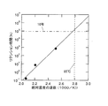
実施例2において、210℃、180℃及び125℃の環境下で、抵抗変化層106の抵抗値の変化を測定した。低抵抗状態に設定した場合は初期の抵抗値と比較してそれほど変化は大きくなかったのに対し、高抵抗に設定した場合は変化が見られた。従って、本発明の第1の実施の形態に係る不揮発性記憶素子100のリテンション特性は、高抵抗値側の変化で律速されていると考えられる。なお、初期状態における高抵抗値及び低抵抗値の1/2の抵抗値を基準とし、これに到達するまで時間を測定すると、210℃の場合では約0.15時間、180℃の場合では7時間、125℃の場合では700時間であった。
In Example 2, the change in resistance value of the
図13は、温度及びリテンション時間のアレニウスプロットを示している。この図13から、85℃以下の環境下では10年を超えるリテンション時間と推定される。このことから、本実施の形態の不揮発性記憶素子は、非常に高いリテンション特性を有していることが分かる。
(第2の実施の形態)
第1の実施の形態では、第1のタンタル酸化物層をスパッタリング装置内で堆積したあと、連続して酸素プラズマによる酸化処理を行い、第2のタンタル酸化物層を形成した。しかし、この方法では使用した装置の都合上、厚い第2のタンタル酸化物層を形成する事はできなかった。そこで、本実施の形態では、膜厚の厚い第2のタンタル酸化物層を形成した場合の不揮発性記憶素子の動作について述べる。
FIG. 13 shows an Arrhenius plot of temperature and retention time. From FIG. 13, it is estimated that the retention time exceeds 10 years in an environment of 85 ° C. or lower. From this, it can be seen that the nonvolatile memory element of this embodiment has very high retention characteristics.
(Second Embodiment)
In the first embodiment, after the first tantalum oxide layer is deposited in the sputtering apparatus, the second tantalum oxide layer is formed by continuously performing an oxidation process using oxygen plasma. However, in this method, a thick second tantalum oxide layer could not be formed because of the equipment used. Thus, in this embodiment, the operation of the nonvolatile memory element in the case where the second tantalum oxide layer having a large thickness is formed will be described.
[不揮発性記憶素子の製造方法]
不揮発性記憶素子の製造方法は、基本的に第1の実施の形態と同一である。但し、酸化工程の都合上、タンタル酸化物の堆積条件や、形成した不揮発性記憶素子のサイズは第1の実施の形態とは異なっている。以下、図2を参照しながら不揮発性素子の製造工程について説明する。
[Method of Manufacturing Nonvolatile Memory Element]
The method for manufacturing the nonvolatile memory element is basically the same as that in the first embodiment. However, for the convenience of the oxidation process, the deposition conditions of tantalum oxide and the size of the formed nonvolatile memory element are different from those of the first embodiment. Hereinafter, a manufacturing process of the nonvolatile element will be described with reference to FIG.
まず、図2(a)に示したように、単結晶シリコンである基板101上に、厚さ200nmの酸化物層102を熱酸化法により形成する。そして、第1電極層103としての厚さ100nmのPt薄膜を、スパッタリング法により酸化物層102上に形成する。その後、第1電極層103上に、第1のタンタル酸化物層104を、Taターゲットを用いた反応性スパッタリング法で形成する。
First, as shown in FIG. 2A, an
ここで、第1のタンタル酸化物層104は、以下に述べる条件で堆積を行った。すなわち、スパッタリング装置内に基板を設置した後、スパッタリング装置内を8×10⁻⁶Pa程度まで真空引きする。そして、タンタルをターゲットとして、パワーを1.6kW、アルゴンガスを34sccm、酸素ガスを21sccm流して、スパッタリング装置内の圧力を0.17Paに保ち、20秒間スパッタリングを行う。これにより、抵抗率が6mΩcmで酸素含有率が約61at%(TaO1.6)の第1のタンタル酸化物層が30nm堆積できる。
Here, the first
次に、図2(b)のように、その第1のタンタル酸化物層104の最表面を酸化してその表面を改質する。ここで、表3に示すように、酸化処理の方法を変化させる事により、実施例5乃至7を作製した。
Next, as shown in FIG. 2B, the outermost surface of the first
すなわち、実施例5はスパッタリング終了後、装置から基板を取り出し、酸素プラズマ発生装置へと導入し、基板を250℃に昇温した状態で酸素プラズマに晒して酸化処理を行った。実施例6はランプアニール装置へと基板を導入し、基板を300℃に昇温した状態で酸素ガスを流して酸化を行った。これらの酸化処理により、第1のタンタル酸化物層104よりも酸素含有率の高い第2のタンタル酸化物層105が形成される(第2のタンタル酸化物層の膜厚組成についての分析結果は後述する)。一方、実施例7は酸化処理を行っていない比較例である。
That is, in Example 5, after the sputtering was completed, the substrate was taken out from the apparatus and introduced into an oxygen plasma generator, and the substrate was exposed to oxygen plasma while being heated to 250 ° C. to be oxidized. In Example 6, the substrate was introduced into a lamp annealing apparatus, and oxidation was performed by flowing an oxygen gas in a state where the substrate was heated to 300 ° C. By these oxidation treatments, a second
その後、第2のタンタル酸化物層105上に、第2電極層107としての厚さ150nmのPt薄膜をスパッタリング法により形成する。なお、第2のタンタル酸化物層105が大気中で酸化されるのをさけるため、第2電極層107は、第2のタンタル酸化物層105を堆積後速やかに行った。最後に、フォトレジスト工程によって、フォトレジストによるパターン108を形成し、ドライエッチングによって、素子領域109を形成する。ここで素子領域の109は、一辺が0.5μmの四角の形状とした。
[実施例5乃至7の抵抗変化特性]
次に、本実施の形態において実際に作製した実施例5乃至7に対して電気的パルスを印加して、抵抗変化を起こさせた時の特性について説明する。
Thereafter, a Pt thin film having a thickness of 150 nm as the
[Resistance change characteristics of Examples 5 to 7]
Next, characteristics when an electric pulse is applied to Examples 5 to 7 actually manufactured in the present embodiment to cause a resistance change will be described.
図14は、第2の実施の形態に係る不揮発性記憶素子が備える抵抗変化層の抵抗値と印加した電気的パルスとの関係を示す図であり、(a)乃至(c)はそれぞれ実施例5乃至7における測定結果を示している。 FIG. 14 is a diagram showing the relationship between the resistance value of the variable resistance layer included in the nonvolatile memory element according to the second embodiment and the applied electric pulse, and (a) to (c) are examples. The measurement results in 5 to 7 are shown.
まず、酸素プラズマによって酸化処理を行って第2のタンタル酸化物層を形成した実施例5の結果について述べる。図14(a)の結果を見れば分かるように、製造直後の不揮発性記憶素子に負電圧−1.2Vを加えると、初期が約400Ωであった抵抗値が約200Ωに低下し、正電圧1.5Vを加えると抵抗値は2000Ω程度に増加している。すなわち、フォーミング工程なしに抵抗変化が起こっている。その後、負電圧−1.2Vと正電圧1.5Vの電気的パルスを交互に加える事で抵抗値は約200Ωと約3000Ωの間を往復し、良好に抵抗変化が起こっている。
これもフォーミング工程なしで、安定して抵抗変化が起こっている事が分かる。すなわち、初期約600Ωであった抵抗が負電圧−1.2Vを加える事で、300Ω程度に低下し、正電圧1.5Vを加える事で5000Ω程度に増加している。そしてその後は、負電圧−1.2Vと正電圧1.5Vの電気的パルスを交互に加える事で抵抗値は約200Ωと約5000Ωの間を往復し、良好に抵抗変化が起こっている。
First, the result of Example 5 in which the second tantalum oxide layer was formed by performing the oxidation treatment with oxygen plasma will be described. As can be seen from the result of FIG. 14A, when a negative voltage of −1.2 V is applied to the nonvolatile memory element immediately after manufacture, the resistance value, which was initially about 400Ω, is reduced to about 200Ω, and the positive voltage is increased. When 1.5V is applied, the resistance value increases to about 2000Ω. That is, the resistance change occurs without the forming process. Thereafter, by alternately applying electrical pulses of negative voltage -1.2V and positive voltage 1.5V, the resistance value reciprocates between about 200Ω and about 3000Ω, and the resistance change is good.
This also shows that the resistance change is stable without the forming process. That is, the initial resistance of about 600Ω is reduced to about 300Ω by applying a negative voltage of −1.2V, and increased to about 5000Ω by applying a positive voltage of 1.5V. After that, by alternately applying electric pulses of negative voltage -1.2V and positive voltage 1.5V, the resistance value reciprocates between about 200Ω and about 5000Ω, and the resistance change is good.
しかしながら、図14(c)に示した、第1のタンタル酸化物層を酸化していない実施例7は上記とはかなり異なる結果が得られている。すなわち、実施例7は、作製した直後の状態では、実施例5および6よりも高い電圧である、負電圧−1.5Vと正電圧2Vを印加しても全く抵抗変化を示さなかった。そこで、印加電圧を正電圧2.5Vから0.1V刻みで増加させてゆくと(図14(c)の横軸のパルス数で26回目から32回の範囲)、3.2Vの時に抵抗値が約40Ωから約60000Ωに急激に増加しているのが分かる。その後は、負電圧−1.5Vと正電圧2.0Vの電圧の電気的パルスを印加する事で抵抗変化が生じている。ここで、印加電圧を2.5Vから3.2Vへと増加させた工程が、従来技術で開示されているフォーミング工程に相当すると考えられる。すなわちこの工程で第1のタンタル酸化膜層104の表面付近に第2のタンタル酸化物層105に相当する高抵抗層が形成されているのではないかと考えられる。
However, in Example 7 in which the first tantalum oxide layer shown in FIG. 14C is not oxidized, a result quite different from the above is obtained. That is, in Example 7, in the state immediately after fabrication, even when a negative voltage of −1.5 V and a positive voltage of 2 V, which are higher voltages than Examples 5 and 6, were applied, no resistance change was shown. Therefore, when the applied voltage is increased from the positive voltage of 2.5 V in increments of 0.1 V (the range from the 26th to the 32nd in the number of pulses on the horizontal axis in FIG. 14C), the resistance value is 3.2 V. Can be seen to increase rapidly from about 40Ω to about 60000Ω. Thereafter, a resistance change is caused by applying electrical pulses of negative voltage −1.5V and positive voltage 2.0V. Here, the process of increasing the applied voltage from 2.5 V to 3.2 V is considered to correspond to the forming process disclosed in the prior art. That is, it is considered that a high resistance layer corresponding to the second
以上の実施例から明らかなように、第2のタンタル酸化物層を形成しなければ、不揮発性記憶素子は、フォーミング工程無しに動作しない事は明らかである。逆にいえば、フォーミング工程無しに不揮発性記憶素子を動作させるには、第2のタンタル酸化物層の存在は不可欠であると考えられる。 As is clear from the above embodiments, it is clear that the nonvolatile memory element does not operate without the forming process unless the second tantalum oxide layer is formed. Conversely, it is considered that the presence of the second tantalum oxide layer is indispensable for operating the nonvolatile memory element without the forming process.
[抵抗変化層の解析]
本実施の形態における抵抗変化層106の構造を解析するため、単結晶シリコン基板上に厚さ200nmの酸化物層が形成された基板上に、実施例5及び6と全く同じ条件で、タンタル酸化物を堆積して、酸化処理まで行ったサンプルを用意した。これらのサンプルを、それぞれD、Eと表記する。それぞれのサンプルのX線反射率測定の結果を表4に示す。なお、サンプルD及びEは、サンプルA乃至Cと同様に、第2のタンタル酸化物層が露出された状態とした。
[Analysis of variable resistance layer]
In order to analyze the structure of the
表4を参照すると、酸素プラズマで酸化を行ったサンプルDは、第2のタンタル酸化物層TaOyの膜厚が8.1nmと当初の狙いどおり、サンプルA乃至Cに比べて厚くなっている。また、yは2.47となっており、化学量論的組成を有するTa2O5よりも酸素が欠損した状態になっていることが分かる。また、ランプアニール装置で酸化処理を行ったサンプルEでは、第2のタンタル酸化物層TaOyの膜厚が7.3nmで、yが2.38となっている。 Referring to Table 4, Sample D oxidized with oxygen plasma has a second tantalum oxide layer TaO y having a thickness of 8.1 nm, which is thicker than Samples A to C, as originally intended. . Moreover, y is 2.47, which indicates that oxygen is deficient as compared with Ta 2 O 5 having a stoichiometric composition. Further, in sample E subjected to the oxidation treatment by the lamp annealing apparatus, the film thickness of the second tantalum oxide layer TaO y is 7.3 nm and y is 2.38.
ここで、X線反射率測定の結果と不揮発性記憶素子にした時の初期抵抗の値に矛盾がある事に気付く。すなわち、X線反射率測定の結果では、酸素プラズマ酸化処理を行ったサンプルDの膜厚及びyの値が、ランプアニール酸化処理を行ったサンプルEの膜厚及びyの値よりも大きくなっているにも関わらず(表4参照)、初期抵抗は酸素プラズマ酸化処理を行った実施例5の方が、ランプアニール酸化処理を行った実施例6よりも小さくなっている(表3)。現段階で考えられるこの矛盾の原因の一つは、初期抵抗のばらつきにあると考えられる。つまり、ある程度偶発的に実施例5の初期抵抗が実施例6の初期抵抗よりも小さくなったと考えられる。もう一つの考えられる原因は第2のタンタル酸化物層の膜質である。本実施の形態では、第2のタンタル酸化物層の膜厚と組成は評価したが、欠陥の評価等は測定が非常に困難なため行えていない。一般にプラズマ中で酸化膜を形成した場合、ランプアニール等の通常の酸化工程に比べて欠陥は多く形成されると考えられる。そして、欠陥が多く形成されれば、その欠陥を介して、電荷が流れる可能性があり、その結果、実施例5の初期抵抗が実施例の6の初期抵抗よりも低くなったと考える事ができるのである。
[不揮発性記憶素子の断面観察]
上述のように、本実施の形態で形成した不揮発性記憶素子の第2のタンタル酸化物層の膜厚は上述のように7〜8nm程度の値である。この程度の膜厚があれば、透過型電子顕微鏡による不揮発性素子の断面観察によって、第2のタンタル酸化物層の存在が容易に観察できる。そこで、実施例5の酸素プラズマ酸化により第2のタンタル酸化物層を形成した不揮発性記憶素子の断面観察を実際に行った。その結果を図15(a)に示す。図15(b)は、図15(a)の写真のスケッチである。
Here, it is noticed that there is a contradiction between the result of the X-ray reflectivity measurement and the value of the initial resistance when the nonvolatile memory element is used. That is, in the result of the X-ray reflectivity measurement, the film thickness and y value of the sample D subjected to the oxygen plasma oxidation treatment are larger than the film thickness and y value of the sample E subjected to the lamp annealing oxidation treatment. Nevertheless (see Table 4), the initial resistance is smaller in Example 5 where the oxygen plasma oxidation treatment is performed than in Example 6 where the lamp annealing oxidation treatment is performed (Table 3). One possible cause of this contradiction at this stage is thought to be the variation in initial resistance. In other words, it is considered that the initial resistance of Example 5 was somewhat smaller than the initial resistance of Example 6 by some chance. Another possible cause is the film quality of the second tantalum oxide layer. In the present embodiment, the thickness and composition of the second tantalum oxide layer are evaluated, but the evaluation of defects and the like cannot be performed because measurement is very difficult. In general, when an oxide film is formed in plasma, it is considered that more defects are formed than in a normal oxidation process such as lamp annealing. If a large number of defects are formed, charge may flow through the defects. As a result, it can be considered that the initial resistance of Example 5 is lower than the initial resistance of Example 6. It is.
[Section observation of non-volatile memory element]
As described above, the thickness of the second tantalum oxide layer of the nonvolatile memory element formed in this embodiment has a value of about 7 to 8 nm as described above. With such a film thickness, the presence of the second tantalum oxide layer can be easily observed by observing the cross section of the nonvolatile element with a transmission electron microscope. Therefore, a cross-sectional observation of the nonvolatile memory element in which the second tantalum oxide layer was formed by oxygen plasma oxidation of Example 5 was actually performed. The result is shown in FIG. FIG. 15B is a sketch of the photograph of FIG.
これらの図を見ると明らかなように、Ptから成る第1電極(第1電極層)、第1のタンタル酸化物層、第2のタンタル酸化物層、Ptから成る第2電極(第2電極層)が明確に確認できる。さらに第1のタンタル酸化物層の膜厚は若干のばらつきはあるが約28nm、第2のタンタル酸化物層の膜厚は約8nm程度となっている事も分かる。これらの値は、同一の酸化条件で作製したサンプルDのX線反射率測定の結果とほぼ一致している(表4より、第1のタンタル酸化物層の膜厚26.6nm、第2のタンタル酸化物層の膜厚8.1nm)。以上の事から、本実施の形態の方法で作製した不揮発性記憶素子には、実際に第2のタンタル酸化物層が存在している事が明らかとなった。また、X線反射率測定による分析結果の妥当性の証明ともなっている。また、サンプルA〜Eのデータを総合すると、第2のタンタル酸化物層の厚みは、実質的に1nm以上8nm以下(正確には1.1nm以上8.1nm以下)が好ましいことが実証された。
(第3の実施の形態)
上述した第1の実施の形態に係る不揮発性記憶素子100の場合、第1のタンタル酸化物層104の酸素含有率は58at%(TaO1.4)であった。また第2の実施の形態に係る不揮発性記憶素子100の第1のタンタル酸化物層104の酸素含有率もこれに近く、61at%(TaO1.6)であった。これに対し、第3の実施の形態に係る不揮発性記憶素子は、もう少し大きく酸素含有率を変化させた第1のタンタル酸化物層を備えている。第3の実施の形態のその他の構成については、第1及び第2の実施の形態の場合と同様であるので、図示は省略する。以下、図1を参照しながら、第1のタンタル酸化物層の酸素含有率を変化させて作製した本実施の形態における各実施例の製造方法及びその抵抗変化特性等について説明する。
As is apparent from these figures, the first electrode (first electrode layer) made of Pt, the first tantalum oxide layer, the second tantalum oxide layer, and the second electrode (second electrode made of Pt). Layer) can be clearly seen. Further, it can be seen that the film thickness of the first tantalum oxide layer is about 28 nm although there is some variation, and the film thickness of the second tantalum oxide layer is about 8 nm. These values almost coincide with the result of the X-ray reflectivity measurement of Sample D produced under the same oxidation conditions (from Table 4, the first tantalum oxide layer has a film thickness of 26.6 nm, the second The film thickness of the tantalum oxide layer is 8.1 nm). From the above, it has been clarified that the second tantalum oxide layer actually exists in the nonvolatile memory element manufactured by the method of this embodiment. It also proves the validity of the analysis result by X-ray reflectivity measurement. In addition, when the data of samples A to E are combined, it has been demonstrated that the thickness of the second tantalum oxide layer is preferably 1 nm or more and 8 nm or less (more precisely, 1.1 nm or more and 8.1 nm or less). .
(Third embodiment)
In the case of the
[スパッタリング時の酸素流量比と組成との関係]
まず、本実施の形態におけるタンタル酸化物の作製条件及び酸素含有率の解析結果について述べる。タンタルの酸化物は、第1の実施の形態で説明した方法と同様の方法で作製した。但し、タンタル酸化物の酸素含有率は、スパッタリング時の酸素流量比を調整することで制御する。具体的なスパッタリング時の工程に従って説明すると、まず、スパッタリング装置内に基板を設置し、スパッタリング装置内を7×10⁻⁴Pa程度まで真空引きする。そして、タンタルをターゲットとして、パワーを250W、アルゴンガスと酸素ガスとをあわせた全ガス圧力を3.3Pa、基板の設定温度を30℃にし、スパッタリングを行う。ここでは、酸素ガスの流量比を0.8%から6.7%まで変化させている。まずは、組成を調べる事が目的であるため、基板としては、Si上にSiO2を200nm堆積したものを用い、タンタル酸化物層の膜厚は約100nmになるようにスパッタリング時間を調整した。また、第1の実施の形態で説明したような、酸素プラズマへの暴露は行っていない。このようにして作製したタンタル酸化物層の組成をラザフォード後方散乱法(RBS法)、及びオージェ電子分光法(AES法)によって解析した結果を図16に示す。この図から、酸素分圧比を0.8%から6.7%に変化させた場合、タンタル酸化物層中の酸素含有率は約40at%(TaO0.66)から約70at%(TaO2.3)へと変化していることが分かる。すなわち、タンタル酸化物層中の酸素含有率を酸素流量比によって制御可能であることが分かる。
[Relationship between oxygen flow ratio and composition during sputtering]
First, conditions for producing tantalum oxide and an analysis result of oxygen content in this embodiment will be described. The tantalum oxide was manufactured by a method similar to the method described in the first embodiment. However, the oxygen content of the tantalum oxide is controlled by adjusting the oxygen flow rate ratio during sputtering. The description will be made according to a specific sputtering process. First, a substrate is placed in a sputtering apparatus, and the inside of the sputtering apparatus is evacuated to about 7 × 10 −4 Pa. Then, using tantalum as a target, sputtering is performed with a power of 250 W, a total gas pressure of argon gas and oxygen gas of 3.3 Pa, and a set temperature of the substrate of 30 ° C. Here, the flow rate ratio of oxygen gas is changed from 0.8% to 6.7%. First, since the purpose is to examine the composition, a substrate in which 200 nm of SiO 2 was deposited on Si was used, and the sputtering time was adjusted so that the film thickness of the tantalum oxide layer was about 100 nm. Further, exposure to oxygen plasma as described in the first embodiment is not performed. FIG. 16 shows the result of analyzing the composition of the tantalum oxide layer thus prepared by Rutherford backscattering method (RBS method) and Auger electron spectroscopy (AES method). From this figure, when the oxygen partial pressure ratio is changed from 0.8% to 6.7%, the oxygen content in the tantalum oxide layer is changed from about 40 at% (TaO 0.66 ) to about 70 at% (TaO 2.3 ). You can see that it is changing. That is, it can be seen that the oxygen content in the tantalum oxide layer can be controlled by the oxygen flow rate ratio.
なお、組成測定用に用意した試料は、基板上に堆積後、測定までの間に大気中の酸素によって酸化され、表面に高酸素含有率層が形成されていると考えられる。しかしながら、RBS及びAESの測定を行う前に、表面をエッチングして測定を行ったので、この表面の高酸素含有率層が、酸素含有率の測定に与える影響は無視しうる。 Note that it is considered that the sample prepared for composition measurement is oxidized by oxygen in the atmosphere after being deposited on the substrate and before measurement, and a high oxygen content layer is formed on the surface. However, since the surface was etched before measurement of RBS and AES, the influence of the high oxygen content layer on the surface on the measurement of the oxygen content can be ignored.
なお、本実施の形態では、タンタル酸化物層の解析にラザフォード後方散乱法(RBS)及びオージェ電子分光法(AES)を利用したが、蛍光X線分析法(XPS)や電子線マイクロアナリシス法(EPMA)等の機器分析手法も利用可能である。 In this embodiment, Rutherford backscattering (RBS) and Auger electron spectroscopy (AES) are used for analysis of the tantalum oxide layer, but X-ray fluorescence (XPS) or electron microanalysis ( An instrumental analysis technique such as EPMA) can also be used.
[第1のタンタル酸化物層の組成と抵抗変化特性]
次に、酸素含有率を変化させたタンタル酸化物層を、第1のタンタル酸化物層104として用いて抵抗変化層106を形成し、本実施の形態の不揮発性記憶素子100を構成した場合の抵抗変化特性について説明する。不揮発性記憶素子100の作製は、第1の実施の形態で説明した方法と同様の方法を用いた。すなわち、単結晶シリコン基板101上に、厚さ200nmの酸化物層102を熱酸化法により形成し、第1電極層103としての厚さ100nmのPt薄膜を、スパッタリング法により酸化物層102上に形成する。その後、第1電極層103上に、タンタルをターゲットとして、パワーを250W、アルゴンガスと酸素ガスとをあわせた全ガス圧力を3.3Pa、基板の設定温度を30℃としてスパッタリングを行い、第1のタンタル酸化物層104を形成する。本実施の形態で検討した範囲では、酸素ガスの流量比を、0.8%から6.7%まで変化させて各実施例を作製した。
[Composition and resistance change characteristics of first tantalum oxide layer]
Next, when the
第1のタンタル酸化物層104の膜厚は30nmになるようにスパッタリング時間を調節した。その後、第1のタンタル酸化物層104の最表面に対して酸素プラズマを30秒間照射し、第2のタンタル酸化物層105を形成した。最後に、第2のタンタル酸化物層105上に、第2電極層107としての厚さ150nmのPt薄膜をスパッタ法により形成して、不揮発記憶素子100を作製した。
The sputtering time was adjusted so that the film thickness of the first
以上のように作製した不揮発性記憶素子の抵抗変化現象を測定した。その結果、図16のα点(酸素流量比約1.7%、酸素含有率約45at%)からβ点(酸素流量比約5%、酸素含有率約65at%)のタンタル酸化膜を使った不揮発性記憶素子では、高抵抗値が低抵抗値の5倍以上と良好であった。 The resistance change phenomenon of the nonvolatile memory element manufactured as described above was measured. As a result, the tantalum oxide film from the α point (oxygen flow rate ratio: about 1.7%, oxygen content rate: about 45 at%) to β point (oxygen flow rate ratio: about 5%, oxygen content rate: about 65 at%) in FIG. In the nonvolatile memory element, the high resistance value was as good as 5 times the low resistance value.
図17(a)と(b)は、それぞれ、α点およびβ点の酸素含有率を有する試料についてのパルス印加回数に対する抵抗変化特性を測定した結果である。図17(b)および図17(c)によれば、α点およびβ点の酸素含有率においては、共に、高抵抗値が低抵抗値の5倍以上と良好であることが判る。従って、酸素含有率が45〜65at%の組成範囲、即ち抵抗変化層をTaOxと表記した場合におけるxの範囲が0.8≦x≦1.9の範囲がより適切な抵抗変化層の範囲である(酸素含有率=45at%がx=0.8に、酸素含有率=65at%がx=1.9にそれぞれ対応)。なお、RBS法による組成分析では、酸素含有量の分析値は±5at%程度の精度である。従って、前記xの組成範囲もこの精度に起因する測定誤差を含んでおり、実際には、酸素含有率が40〜70at%の組成範囲までこの適切な組成範囲である可能性がある。この組成範囲以外でも抵抗変化現象は確認され又は推認されるが、この組成範囲内に比べると抵抗率が小さくなり又は大きくなることから高抵抗値が低抵抗値の5倍未満になると考えられ、記憶素子として動作の安定性にやや欠けると考えられる。 FIGS. 17A and 17B show the results of measuring resistance change characteristics with respect to the number of pulse applications for a sample having oxygen content at the α point and the β point, respectively. According to FIG. 17B and FIG. 17C, it can be seen that both the high and low resistance values of the oxygen content at the α point and the β point are as good as 5 times the low resistance value. Therefore, the composition range in which the oxygen content is 45 to 65 at%, that is, the range of x ≦ 0.8 ≦ x ≦ 1.9 when the resistance change layer is expressed as TaO x is a more appropriate range of the resistance change layer. (Oxygen content = 45 at% corresponds to x = 0.8 and oxygen content = 65 at% corresponds to x = 1.9). In the composition analysis by the RBS method, the analysis value of the oxygen content has an accuracy of about ± 5 at%. Therefore, the composition range of x also includes a measurement error due to this accuracy, and in fact, there is a possibility that this composition range is an appropriate composition range up to a composition range where the oxygen content is 40 to 70 at%. Although the resistance change phenomenon is confirmed or inferred even outside this composition range, it is considered that the high resistance value is less than 5 times the low resistance value because the resistivity becomes smaller or larger than within this composition range, It is considered that the operation stability is somewhat lacking as a memory element.
なお、第1の実施の形態では、図1に示したとおり、抵抗変化層106が、下方に設けられた第1電極層103と、上方に設けられた第2電極層107とによって挟まれるように構成されており、しかも抵抗変化層106の両端部と第2電極層107の両端部とが断面視で揃っているが、これは一例であり、本発明はこのような構成に限定されるわけではない。以下、その変形例について説明する。
In the first embodiment, as shown in FIG. 1, the
図18(a)から(c)は、本発明の第1の実施の形態に係る不揮発性記憶素子の変形例の構成を示す断面図である。なお、これらの図18(a)から(c)においては、基板および酸化物層を便宜上省略している。また、いくつかのタンタル酸化物層からなる抵抗変化層は、一つの層として表現してある。実際にはこの抵抗変化層は、図1もしくは図8に示されたような層構造を取る。 FIGS. 18A to 18C are cross-sectional views showing a configuration of a modification of the nonvolatile memory element according to the first embodiment of the present invention. In FIGS. 18A to 18C, the substrate and the oxide layer are omitted for convenience. In addition, the resistance change layer including several tantalum oxide layers is expressed as one layer. Actually, this variable resistance layer has a layer structure as shown in FIG. 1 or FIG.
図18(a)に示す変形例では、第1電極層103D、抵抗変化層106D、および第2電極層107Dがこの順に積層されて構成されており、これらの第1電極層103D、抵抗変化層106D、および第2電極層107Dの両端部は断面視で揃っていない。これに対し、図18(b)に示す変形例では、同じく第1電極層103E、抵抗変化層106E、および第2電極層107Eが積層されて構成されているものの、これらの第1電極層103E、抵抗変化層106E、および第2電極層107Eの両端部が断面視ですべて揃っている。本発明の不揮発性記憶素子は、このように構成されていてもよい。
In the modification shown in FIG. 18A, the
また、本実施の形態に係る不揮発性記憶素子100、および上記の2つの変形例においては、いずれも抵抗変化層が上下に配された電極で挟まれるように構成されているが、抵抗変化層の両端面に電極を形成することによって、抵抗変化層の主面に平行な方向に電流を流すような構成であってもよい。すなわち、図18(c)に示すように、抵抗変化層104Fの一方の端面に第1電極層103Fを、他方の端面に第2電極層107Fをそれぞれ形成し、その抵抗変化層106Fの主面に平行な方向に電流を流すように構成されていてもよい。
Further, in the
ところで、図示していないが、本実施の形態に係る不揮発性記憶素子は層間絶縁層を備えている。なお、化学気相堆積法などによって弗素ドープの酸化膜を形成し、これを層間絶縁層とするようにしてもよい。また、層間絶縁層を備えない構成であってもよい。 Although not shown, the nonvolatile memory element according to this embodiment includes an interlayer insulating layer. Note that a fluorine-doped oxide film may be formed by chemical vapor deposition or the like and used as an interlayer insulating layer. Moreover, the structure which is not provided with an interlayer insulation layer may be sufficient.
また、同様にして、図示していないが、本実施の形態に係る不揮発性記憶素子は配線層を備えている。配線材料としては、例えば、Pt、Ir、Pd、Ag、Au、Cu、W、Ni、チッ化Tiなどを用いることができる。なお、この配線層を備えない構成であってもよい。 Similarly, although not shown, the nonvolatile memory element according to this embodiment includes a wiring layer. As the wiring material, for example, Pt, Ir, Pd, Ag, Au, Cu, W, Ni, Ti nitride, or the like can be used. Note that the wiring layer may not be provided.
また、上記の本実施の形態1乃至3における酸素ガスの分圧比をはじめとするスパッタリングの条件は、これらの値に限定されるものではなく、装置の構成や状態に依存して変化するものである。また、第1のタンタル酸化物層の堆積は、Taをターゲットとして利用したが、タンタル酸化物をターゲットとすることによって、酸素などの反応性ガスを使用しないスパッタ法を用いるようにしてもよい。スパッタリング時のパワーやガス圧力、基板温度等も上記の条件に限定されるものではない。さらに、化学気相堆積法等の成膜技術を用いて第1のタンタル酸化物層を形成しても良い。 Further, the sputtering conditions including the oxygen gas partial pressure ratio in the first to third embodiments are not limited to these values, but vary depending on the configuration and state of the apparatus. is there. The first tantalum oxide layer is deposited using Ta as a target. However, by using tantalum oxide as a target, a sputtering method that does not use a reactive gas such as oxygen may be used. The power, gas pressure, substrate temperature, and the like during sputtering are not limited to the above conditions. Further, the first tantalum oxide layer may be formed using a film formation technique such as chemical vapor deposition.
また、実施の形態1及び2では、酸素プラズマ処理及び酸化によって、第2のタンタル酸化物層を形成したが、これ以外の、オゾンによる酸化、空気中での自然酸化、及び、基板に吸着した水等の分子との反応を利用しての酸化等の方法を用いても良い。さらに、第2のタンタル酸化物層自体をスパッタリングや、化学気相堆積法等の成膜技術を使って形成しても良い。 In the first and second embodiments, the second tantalum oxide layer is formed by oxygen plasma treatment and oxidation, but other than this, oxidation by ozone, natural oxidation in air, and adsorption to the substrate. A method such as oxidation using a reaction with a molecule such as water may be used. Further, the second tantalum oxide layer itself may be formed using a film formation technique such as sputtering or chemical vapor deposition.
(第4の実施の形態)
上述した第1乃至第3の実施の形態に係る不揮発性記憶素子は、種々の形態の不揮発性半導体装置へ適用することが可能である。第4の実施の形態に係る半導体装置は、第1乃至3の実施の形態に係る不揮発性記憶素子を備える不揮発性半導体装置であって、ワード線とビット線との交点(立体交差点)にアクティブ層を介在させた、いわゆるクロスポイント型のものである。
(Fourth embodiment)
The nonvolatile memory elements according to the first to third embodiments described above can be applied to various types of nonvolatile semiconductor devices. The semiconductor device according to the fourth embodiment is a nonvolatile semiconductor device including the nonvolatile memory elements according to the first to third embodiments, and is active at an intersection (steric intersection) between a word line and a bit line. It is a so-called cross-point type with a layer interposed.
[第4の実施の形態に係る半導体装置の構成]
図19は、本発明の第4の実施の形態に係る不揮発性半導体装置の構成を示すブロック図である。また、図20は、図19におけるA部の構成(4ビット分の構成)を示す斜視図である。
[Configuration of Semiconductor Device According to Fourth Embodiment]
FIG. 19 is a block diagram showing a configuration of a nonvolatile semiconductor device according to the fourth embodiment of the present invention. FIG. 20 is a perspective view showing the configuration (configuration corresponding to 4 bits) of part A in FIG.
図19に示すように、本実施の形態に係る不揮発性半導体装置200は、半導体基板上に、メモリ本体部201を備えており、このメモリ本体部201は、メモリアレイ202と、行選択回路/ドライバ203と、列選択回路/ドライバ204と、情報の書き込みを行うための書き込み回路205と、選択ビット線に流れる電流量を検出し、データ「1」または「0」と判定するセンスアンプ206と、端子DQを介して入出力データの入出力処理を行うデータ入出力回路207とを具備している。また、不揮発性半導体装置200は、外部から入力されるアドレス信号を受け取るアドレス入力回路208と、外部から入力されるコントロール信号に基づいて、メモリ本体部201の動作を制御する制御回路209とをさらに備えている。
As shown in FIG. 19, a
メモリアレイ202は、図19および図20に示すように、半導体基板の上に互いに平行に形成された複数のワード線WL0,WL1,WL2,…と、これらの複数のワード線WL0,WL1,WL2,…の上方にその半導体基板の主面に平行な面内において互いに平行に、しかも複数のワード線WL0,WL1,WL2,…に立体交差するように形成された複数のビット線BL0,BL1,BL2,…とを備えている。
As shown in FIGS. 19 and 20, the
また、これらの複数のワード線WL0,WL1,WL2,…と複数のビット線BL0,BL1,BL2,…との立体交差点に対応してマトリクス状に設けられた複数のメモリセルM111,M112,M113,M121,M122,M123,M131,M132,M133,…(以下、「メモリセルM111,M112,…」と表す)が設けられている。 Further, a plurality of memory cells M111, M112, M113 provided in a matrix corresponding to the solid intersections of the plurality of word lines WL0, WL1, WL2,... And the plurality of bit lines BL0, BL1, BL2,. , M121, M122, M123, M131, M132, M133,... (Hereinafter referred to as “memory cells M111, M112,...”).
ここで、メモリセルM111,M112,…は、第1の実施の形態に係る不揮発性記憶素子に相当し、タンタル酸化物を含む抵抗変化層を有している。ただし、本実施の形態において、これらのメモリセルM111,M112,…は、後述するように、電流抑制素子を備えている。 Here, the memory cells M111, M112,... Correspond to the nonvolatile memory element according to the first embodiment, and have a resistance change layer containing tantalum oxide. However, in the present embodiment, these memory cells M111, M112,... Have a current suppressing element as will be described later.
なお、図19におけるメモリセルM111,M112,…は、図20において符号21
0で示されている。
Note that memory cells M111, M112,... In FIG.
It is shown as zero.
アドレス入力回路208は、外部回路(図示せず)からアドレス信号を受け取り、このアドレス信号に基づいて行アドレス信号を行選択回路/ドライバ203へ出力するとともに、列アドレス信号を列選択回路/ドライバ204へ出力する。ここで、アドレス信号は、複数のメモリセルM111,M112,…のうちの選択される特定のメモリセルのアドレスを示す信号である。また、行アドレス信号は、アドレス信号に示されたアドレスのうちの行のアドレスを示す信号であり、列アドレス信号は、アドレス信号に示されたアドレスのうちの列のアドレスを示す信号である。
The
制御回路209は、情報の書き込みサイクルにおいては、データ入出力回路207に入力された入力データDinに応じて、書き込み用電圧の印加を指示する書き込み信号を書き込み回路205へ出力する。他方、情報の読み出しサイクルにおいて、制御回路209は、読み出し用電圧の印加を指示する読み出し信号を列選択回路/ドライバ204へ出力する。
In the information write cycle, the
行選択回路/ドライバ203は、アドレス入力回路208から出力された行アドレス信号を受け取り、この行アドレス信号に応じて、複数のワード線WL0,WL1,WL2,…のうちの何れかを選択し、その選択されたワード線に対して、所定の電圧を印加する。
The row selection circuit /
また、列選択回路/ドライバ204は、アドレス入力回路208から出力された列アドレス信号を受け取り、この列アドレス信号に応じて、複数のビット線BL0,BL1,BL2,…のうちの何れかを選択し、その選択されたビット線に対して、書き込み用電圧または読み出し用電圧を印加する。
Further, the column selection circuit /
書き込み回路205は、制御回路209から出力された書き込み信号を受け取った場合、行選択回路/ドライバ203に対して選択されたワード線に対する電圧の印加を指示する信号を出力するとともに、列選択回路/ドライバ204に対して選択されたビット線に対して書き込み用電圧の印加を指示する信号を出力する。
When the
また、センスアンプ206は、情報の読み出しサイクルにおいて、読み出し対象となる選択ビット線に流れる電流量を検出し、データ「1」または「0」と判定する。その結果得られた出力データDOは、データ入出力回路207を介して、外部回路へ出力される。
Further, the
[第4の実施の形態に係る不揮発性半導体装置が備える不揮発性記憶素子の構成]
図21は、本発明の第4の実施の形態に係る不揮発性半導体装置が備える不揮発性記憶素子の構成を示す断面図である。なお、図21では、図20のB部における構成が示されている。
[Configuration of Nonvolatile Memory Element Provided in Nonvolatile Semiconductor Device According to Fourth Embodiment]
FIG. 21 is a cross-sectional view showing a configuration of a nonvolatile memory element included in the nonvolatile semiconductor device according to the fourth embodiment of the present invention. Note that FIG. 21 shows the configuration in the B part of FIG.
図21に示すように、本実施の形態に係る不揮発性半導体装置が備える不揮発性記憶素子210は、銅配線である下部配線212(図20におけるワード線WL1に相当する)と同じく上部配線211(図20におけるビット線BL1に相当する)との間に介在しており、下部電極217と、電流抑制素子216と、内部電極215と、抵抗変化層214と、上部電極213とがこの順に積層されて構成されている。
As shown in FIG. 21, the
ここで、内部電極215、抵抗変化層214、および上部電極213は、図1及び図20に示した実施の形態1乃至3に係る不揮発性記憶素子100における第1電極層103、抵抗変化層106、および第2電極層105にそれぞれ相当する。したがって、抵抗変化層214は、第1乃至第3の実施の形態と同様にして形成される。
Here, the
電流抑制素子216は、内部電極215を介して、抵抗変化層214と直列接続されている。この電流抑制素子216は、ダイオードに代表される素子であり、電圧に対して非線形な電流特性を示すものである。また、この電流抑制素子216は、電圧に対して双方向性の電流特性を有しており、所定の閾値電圧Vf(一方の電極を基準にして例えば+1V以上または−1V以下)で導通するように構成されている。
The
なお、タンタルおよびその酸化物は、半導体プロセスに一般的に用いられている材料であり、非常に親和性が高いといえる。そのため、既存の半導体製造プロセスに容易に組み入れることが可能である。 Note that tantalum and its oxide are materials generally used in semiconductor processes and can be said to have very high affinity. Therefore, it can be easily incorporated into an existing semiconductor manufacturing process.
[第4の実施の形態に係る不揮発性半導体装置が備える不揮発性記憶素子の変形例の構成]
本実施の形態に係る不揮発性半導体装置が備える不揮発性記憶素子の構成は、図21に示したものに限られるわけではなく、以下に示すような構成であってもよい。
[Configuration of Modification of Nonvolatile Memory Element Provided in Nonvolatile Semiconductor Device According to Fourth Embodiment]
The configuration of the nonvolatile memory element included in the nonvolatile semiconductor device according to the present embodiment is not limited to that shown in FIG. 21 and may be the following configuration.
図22(a)から(g)は、本発明の第4の実施の形態に係る不揮発性半導体装置が備える不揮発性記憶素子の変形例の構成を示す断面図である。 FIGS. 22A to 22G are cross-sectional views showing a configuration of a modified example of the nonvolatile memory element included in the nonvolatile semiconductor device according to the fourth embodiment of the present invention.
図22(a)には、図21に示す構成と異なり、内部電極を備えず、抵抗変化層214が電流抑制素子216の上に形成されている構成が示されている。
FIG. 22A shows a configuration in which the
図22(b)は、図21に示す構成と異なり、下部電極、内部電極、および上部電極を備えず、抵抗変化層214が電流抑制素子216の上に形成されている構成が示されている。また、図22(c)には、図21に示す構成と異なり、下部電極を備えていない構成が示されている。他方、図示はしないが、上部電極を備えていない構成も考えられる。
FIG. 22B shows a configuration in which the
図22(d)には、図21に示す構成と異なり、内部電極および電流抑制素子を備えていない構成が示されており、図22(e)には、さらに上部電極および下部電極を備えていない構成が示されている。 FIG. 22 (d) shows a configuration that does not include an internal electrode and a current suppressing element, unlike the configuration shown in FIG. 21, and FIG. 22 (e) further includes an upper electrode and a lower electrode. There is no configuration shown.
また、図22(f)には、図21に示す構成と異なり、内部電極を備えず、その代わりにオーミック抵抗層218を備える構成が示されており、図22(g)には、内部電極の代わりに第2の抵抗変化層219を備える構成が示されている。
Further, FIG. 22 (f) shows a configuration in which an internal electrode is not provided and an
なお、以上に示した変形例において、上部電極を備えていない場合は上部配線211が不揮発性記憶素子の上部電極として機能し、また、下部電極を備えていない場合は下部配線212が不揮発性記憶素子の下部電極として機能することになる。
In the modification shown above, when the upper electrode is not provided, the
また、メモリセルの数が比較的少ない場合、選択されないメモリセルへの回り込み電流が少なくなる。このような場合、上述したような電流抑制素子を備えない構成とすることが考えられる。 In addition, when the number of memory cells is relatively small, the sneak current to unselected memory cells is reduced. In such a case, it can be considered that the current suppressing element as described above is not provided.
以上のように、本実施の形態に係る不揮発性半導体装置が備える不揮発性記憶素子については、種々の構成が考えられる。 As described above, various configurations of the nonvolatile memory element included in the nonvolatile semiconductor device according to this embodiment can be considered.
[多層化構造の不揮発性半導体装置の構成例]
図19および図20に示した本実施の形態に係る不揮発性半導体装置におけるメモリアレイを、3次元に積み重ねることによって、多層化構造の不揮発性半導体装置を実現することができる。
[Configuration Example of Multilayer Nonvolatile Semiconductor Device]
By stacking the memory arrays in the nonvolatile semiconductor device according to the present embodiment shown in FIGS. 19 and 20 three-dimensionally, a multilayered nonvolatile semiconductor device can be realized.
図23は、本発明の多層化構造の不揮発性半導体装置が備えるメモリアレイの構成を示す斜視図である。図23に示すように、この不揮発性半導体装置は、図示しない半導体基板の上に互いに平行に形成された複数の下部配線212と、これらの複数の下部配線212の上方にその半導体基板の主面に平行な面内において互いに平行に、しかも複数の下部配線212に立体交差するように形成された複数の上部配線211と、これらの複数の下部配線212と複数の上部配線211との立体交差点に対応してマトリクス状に設けられた複数のメモリセル210とを備えるメモリアレイが、複数積層されてなる多層化メモリアレイを備えている。
FIG. 23 is a perspective view showing the configuration of a memory array provided in the multilayered nonvolatile semiconductor device of the present invention. As shown in FIG. 23, the nonvolatile semiconductor device includes a plurality of
なお、図23に示す例では、配線層が5層であり、その立体交差点に配される不揮発性記憶素子が4層の構成となっているが、必要に応じてこれらの層数を増減してもよいことは勿論である。 In the example shown in FIG. 23, the wiring layer has five layers and the nonvolatile memory element arranged at the three-dimensional intersection has a four-layer structure. However, the number of these layers may be increased or decreased as necessary. Of course, it may be.
このように構成された多層化メモリアレイを設けることによって、超大容量不揮発性メモリを実現することが可能となる。 By providing the multi-layered memory array configured as described above, it is possible to realize an ultra-large capacity nonvolatile memory.
なお、第1乃至第3の実施の形態において説明したように、本発明における抵抗変化層は低温で成膜することが可能である。したがって、本実施の形態で示すような配線工程での積層化を行う場合であっても、下層工程で形成されたトランジスタおよびシリサイドなどの配線材料に影響を与えることがないため、多層化メモリアレイを容易に実現することができる。すなわち、本発明のタンタル酸化物を含む抵抗変化層を用いることによって、多層化構造の不揮発性半導体装置を容易に実現することが可能となる。 As described in the first to third embodiments, the variable resistance layer in the present invention can be formed at a low temperature. Therefore, even when stacking is performed in the wiring process as shown in the present embodiment, it does not affect the wiring material such as a transistor and silicide formed in the lower layer process. Can be easily realized. That is, by using the variable resistance layer containing the tantalum oxide of the present invention, it becomes possible to easily realize a nonvolatile semiconductor device having a multilayer structure.
[不揮発性半導体装置の動作例]
次に、情報を書き込む場合の書き込みサイクルおよび情報を読み出す場合の読み出しサイクルにおける第4の実施の形態に係る不揮発性半導体装置の動作例について、図24に示すタイミングチャートを参照しながら説明する。
[Example of operation of nonvolatile semiconductor device]
Next, an operation example of the nonvolatile semiconductor device according to the fourth embodiment in a writing cycle for writing information and a reading cycle for reading information will be described with reference to a timing chart shown in FIG.
図24は、本発明の第4の実施の形態に係る不揮発性半導体装置の動作例を示すタイミングチャートである。なお、ここでは、抵抗変化層が高抵抗状態の場合を情報「1」に、低抵抗状態の場合を情報「0」にそれぞれ割り当てたときの動作例を示す。また、説明の便宜上、メモリセルM111およびM122について情報の書き込みおよび読み出しをする場合のみについて示す。 FIG. 24 is a timing chart showing an operation example of the nonvolatile semiconductor device according to the fourth embodiment of the present invention. Here, an example of operation when the variable resistance layer is assigned to the information “1” when the resistance change layer is in the high resistance state and the information “0” is assigned to the case where the resistance change layer is the low resistance state is shown. For convenience of explanation, only the case where information is written to and read from the memory cells M111 and M122 is shown.
図24におけるVPは、可変抵抗素子と電流抑制素子とで構成されたメモリセルの抵抗変化に必要なパルス電圧を示している。ここでは、VP/2<閾値電圧Vfの関係が成り立つことが望ましい。なぜなら、非選択のメモリセルに回り込んで流れる漏れ電流を抑えることができるからである。その結果、情報を書き込む必要のないメモリセルへ供給される余分な電流を抑制することができ、低消費電流化をより一層図ることができる。また、非選択のメモリセルへの意図しない浅い書き込み(一般にディスターブと称される)が抑制されるなどの利点もある。 VP in FIG. 24 indicates a pulse voltage necessary for resistance change of the memory cell configured by the variable resistance element and the current suppressing element. Here, it is desirable that the relationship of VP / 2 <threshold voltage Vf is satisfied. This is because the leakage current flowing around the unselected memory cells can be suppressed. As a result, it is possible to suppress an excessive current supplied to a memory cell that does not need to write information, and to further reduce current consumption. Further, there is an advantage that unintentional shallow writing (generally referred to as disturb) to unselected memory cells is suppressed.
また、図24において、1回の書き込みサイクルに要する時間である書き込みサイクル時間をtWで、1回の読み出しサイクルに要する時間である読み出しサイクル時間をtRでそれぞれ示している。 In FIG. 24, a write cycle time that is a time required for one write cycle is indicated by tW, and a read cycle time that is a time required for one read cycle is indicated by tR.
メモリセルM111に対する書き込みサイクルにおいて、ワード線WL0にはパルス幅tPのパルス電圧VPが印加され、そのタイミングに応じて、ビット線BL0には同じく0Vの電圧が印加される。これにより、メモリセルM111に情報「1」を書き込む場合の書き込み用電圧が印加され、その結果、メモリセルM111の抵抗変化層が高抵抗化する。すなわち、メモリセルM111に情報「1」が書き込まれたことになる。 In a write cycle for the memory cell M111, a pulse voltage VP having a pulse width tP is applied to the word line WL0, and a voltage of 0V is similarly applied to the bit line BL0 according to the timing. As a result, a write voltage for writing information “1” to the memory cell M111 is applied, and as a result, the resistance change layer of the memory cell M111 has a high resistance. That is, information “1” is written in the memory cell M111.
次に、メモリセルM122に対する書き込みサイクルにおいて、ワード線WL1にはパルス幅tPの0Vの電圧が印加され、そのタイミングに応じて、ビット線BL1には同じくパルス電圧VPが印加される。これにより、M122に情報「0」を書き込む場合の書き込み用電圧が印加され、その結果、メモリセルM122の抵抗変化層が低抵抗化する。すなわち、メモリセルM122に情報「0」が書き込まれたことになる。 Next, in a write cycle for the memory cell M122, a voltage of 0 V having a pulse width tP is applied to the word line WL1, and the pulse voltage VP is similarly applied to the bit line BL1 according to the timing. As a result, a write voltage for writing information “0” to M122 is applied, and as a result, the resistance change layer of the memory cell M122 has a low resistance. That is, information “0” is written in the memory cell M122.
メモリセルM111に対する読み出しサイクルにおいては、書き込み時のパルスよりも振幅が小さいパルス電圧であって、0Vよりも大きくVP/2よりも小さい値の電圧が、ワード線WL0に印加される。また、このタイミングに応じて、書き込み時のパルスよりも振幅が小さいパルス電圧であって、VP/2よりも大きくVPよりも小さい値の電圧が、ビット線BL0に印加される。これにより、高抵抗化されたメモリセルM111の抵抗変化層214の抵抗値に対応した電流が出力され、その出力電流値を検出することにより、情報「1」が読み出される。
In the read cycle for the memory cell M111, a voltage having a smaller amplitude than the pulse at the time of writing and having a value larger than 0V and smaller than VP / 2 is applied to the word line WL0. In accordance with this timing, a pulse voltage having a smaller amplitude than the pulse at the time of writing and having a value larger than VP / 2 and smaller than VP is applied to the bit line BL0. As a result, a current corresponding to the resistance value of the
次に、メモリセルM122に対する読み出しサイクルにおいて、先のメモリセルM111に対する読み出しサイクルと同様の電圧がワード線WL1およびビット線BL1に印加される。これにより、低抵抗化されたメモリセルM122の抵抗変化層214の抵抗値に対応した電流が出力され、その出力電流値を検出することにより、情報「0」が読み出される。
Next, in the read cycle for the memory cell M122, the same voltage as that for the previous read cycle for the memory cell M111 is applied to the word line WL1 and the bit line BL1. As a result, a current corresponding to the resistance value of the
なお、第1の実施の形態において説明したように、本発明におけるタンタル酸化物を含む抵抗変化層を用いた場合、電極間に印加する電気的パルスの幅が20nsec程度の高速パルスであっても、抵抗変化現象を確認することができる。したがって、パルス幅tPは50nsec程度に設定することができる。 As described in the first embodiment, when the variable resistance layer containing tantalum oxide according to the present invention is used, even if the width of the electric pulse applied between the electrodes is a high-speed pulse of about 20 nsec. The resistance change phenomenon can be confirmed. Therefore, the pulse width tP can be set to about 50 nsec.
このようにパルス幅が50nsec程度の高速パルスを用いることができるため、不揮発性半導体装置200の制御回路などの周辺回路の動作時間などを考慮したとしても、1回の書き込みサイクル時間tWは80nsec程度に設定することができる。その場合、例えばデータ入出力回路207の端子DQを介して、不揮発性半導体装置200の外部とのデータの入出力を16ビットで行う場合、情報の書き込みに要するデータ転送速度は、1秒間当たり25Mバイトとなり、非常に高速な書き込み動作を実現することができる。さらに、公知のページモードまたはバーストモードなどの手法を用い、不揮発性半導体装置内部での並列の書き込みビット数を増やすことによって、より一層高速な書き込み動作を実現することも可能である。
Thus, since a high-speed pulse with a pulse width of about 50 nsec can be used, even if the operation time of a peripheral circuit such as a control circuit of the
従来の不揮発性メモリにおいて、比較的高速なデータ転送が可能であるとして知られているNANDフラッシュメモリの場合、上記のページモードを用いたとしても、書き込みに要するデータ転送速度は1秒間当たり10Mバイト程度である。このことからも、本実施の形態の不揮発性半導体装置の書き込み動作の高速性を確認することができる。 In the case of a NAND flash memory that is known to be capable of relatively high-speed data transfer in a conventional non-volatile memory, even if the above page mode is used, the data transfer speed required for writing is 10 Mbytes per second. Degree. This also confirms the high speed of the write operation of the nonvolatile semiconductor device of this embodiment.
また、第1の実施の形態において説明したように、本発明におけるタンタル酸化物を含む抵抗変化層を用いた場合、インプリント性の低い不揮発性記憶素子を実現することができる。すなわち、同一のデータを繰り返し書き込んだ後に、それと逆のデータを書き込む場合であっても、1回の高速パルスで書き換えを行うことができる。そのため、一般的に不揮発性記憶素子で必要とされる消去サイクルまたはリセットサイクルに代表されるような、書き込み前に一方のデータに揃えるステップが不要となる。この点も、本実施の形態における不揮発性半導体装置における書き込みの高速化に寄与する。また、そのようなステップが不要であるため、書き込み動作を単純なステップで行うことが可能となる。 Further, as described in the first embodiment, when the variable resistance layer containing tantalum oxide according to the present invention is used, a nonvolatile memory element with low imprintability can be realized. That is, even when the same data is repeatedly written and then the reverse data is written, the rewriting can be performed with one high-speed pulse. Therefore, a step of aligning with one data before writing, which is typically represented by an erase cycle or a reset cycle required for a nonvolatile memory element, becomes unnecessary. This point also contributes to speeding up writing in the nonvolatile semiconductor device in this embodiment. Further, since such a step is unnecessary, the write operation can be performed in a simple step.
さらに、書き込み用電圧は2〜3V程度の低電圧で足りるため、低消費電力化を実現することもできる。 Further, since a low voltage of about 2 to 3 V is sufficient for the writing voltage, low power consumption can be realized.
本実施の形態においては、半導体基板上に集積したクロスポイント構造のみについて説明している。しかしながら、このような半導体基板上ではなく、プラスチック基板などのより安価な基板上にクロスポイント構造を形成し、バンプ等の組み立て工法で積層化したメモリ装置に適用するようにしてもよい。 In the present embodiment, only the cross point structure integrated on the semiconductor substrate is described. However, the present invention may be applied to a memory device in which a cross-point structure is formed not on such a semiconductor substrate but on a cheaper substrate such as a plastic substrate and stacked by an assembly method such as a bump.
(第5の実施の形態)
上述した第1乃至第3の実施の形態に係る不揮発性記憶素子は、種々の形態の不揮発性半導体装置へ適用することが可能である。第5の実施の形態に係る不揮発性半導体装置は、第1乃至3の実施の形態に係る不揮発性記憶素子を備える不揮発性半導体装置であって、1トランジスタ/1不揮発性記憶部とした、いわゆる1T1R型のものである。
(Fifth embodiment)
The nonvolatile memory elements according to the first to third embodiments described above can be applied to various types of nonvolatile semiconductor devices. The non-volatile semiconductor device according to the fifth embodiment is a non-volatile semiconductor device including the non-volatile memory element according to the first to third embodiments, and is a so-called 1 transistor / 1 non-volatile memory unit. It is of 1T1R type.
[第5の実施の形態に係る不揮発性半導体装置の構成]
図25は、本発明の第5の実施の形態に係る不揮発性半導体装置の構成を示すブロック図である。また、図26は、図25におけるC部の構成(2ビット分の構成)を示す断面図である。
[Configuration of Nonvolatile Semiconductor Device According to Fifth Embodiment]
FIG. 25 is a block diagram showing a configuration of a nonvolatile semiconductor device according to the fifth embodiment of the present invention. FIG. 26 is a cross-sectional view showing the configuration (configuration corresponding to 2 bits) of part C in FIG.
図25に示すように、本実施の形態に係る不揮発性半導体装置300は、半導体基板上に、メモリ本体部301を備えており、このメモリ本体部301は、メモリアレイ302と、行選択回路/ドライバ303と、列選択回路304と、情報の書き込みを行うための書き込み回路305と、選択ビット線に流れる電流量を検出し、データ「1」または「0」と判定するセンスアンプ306と、端子DQを介して入出力データの入出力処理を行うデータ入出力回路307とを具備している。また、不揮発性半導体装置300は、セルプレート電源(VCP電源)308と、外部から入力されるアドレス信号を受け取るアドレス入力回路309と、外部から入力されるコントロール信号に基づいて、メモリ本体部301の動作を制御する制御回路310とをさらに備えている。
As shown in FIG. 25, the
メモリアレイ302は、半導体基板の上に形成された、互いに交差するように配列された複数のワード線WL0,WL1,WL2,…およびビット線BL0,BL1,BL2,…と、これらのワード線WL0,WL1,WL2,…およびビット線BL0,BL1,BL2,…の交点に対応してそれぞれ設けられた複数のトランジスタT11,T12,T13,T21,T22,T23,T31,T32,T33,…(以下、「トランジスタT11,T12,…」と表す)と、トランジスタT11,T12,…と1対1に設けられた複数のメモリセルM211,M212,M213,M221,M222,M223,M231,M232,M233(以下、「メモリセルM211,M212,…」と表す)とを備えている。
The
また、メモリアレイ302は、ワード線WL0,WL1,WL2,…に平行して配列されている複数のプレート線PL0,PL1,PL2,…を備えている。
The
図26に示すように、ワード線WL0,WL1の上方にビット線BL0が配され、そのワード線WL0,WL1とビット線BL0との間に、プレート線PL0,PL1が配されている。 As shown in FIG. 26, a bit line BL0 is disposed above the word lines WL0 and WL1, and plate lines PL0 and PL1 are disposed between the word lines WL0 and WL1 and the bit line BL0.
ここで、メモリセルM211,M212,…は、第1乃至第3の実施の形態に係る不揮発性記憶素子に相当し、タンタル酸化物を含む抵抗変化層を有している。より具体的には、図26における不揮発性記憶素子313が、図25におけるメモリセルM211,M212,…に相当し、この不揮発性記憶素子313は、上部電極314、タンタル酸化物を整含む抵抗変化層315、および下部電極316から構成されている。
Here, the memory cells M211, M212,... Correspond to the nonvolatile memory elements according to the first to third embodiments, and have a resistance change layer containing tantalum oxide. More specifically, the
なお、図26における317はプラグ層を、318は金属配線層を、319はソース/ドレイン領域をそれぞれ示している。
In FIG. 26,
図25に示すように、トランジスタT11,T12,T13,…のドレインはビット線BL0に、トランジスタT21,T22,T23,…のドレインはビット線BL1に、トランジスタT31,T32,T33,…のドレインはビット線BL2に、それぞれ接続されている。 25, the drains of the transistors T11, T12, T13,... Are on the bit line BL0, the drains of the transistors T21, T22, T23,... Are on the bit line BL1, and the drains of the transistors T31, T32, T33,. Each is connected to the bit line BL2.
また、トランジスタT11,T21,T31,…のゲートはワード線WL0に、トランジスタT12,T22,T32,…のゲートはワード線WL1に、トランジスタT13,T23,T33,…のゲートはワード線WL2に、それぞれ接続されている。 In addition, the gates of the transistors T11, T21, T31,... Are on the word line WL0, the gates of the transistors T12, T22, T32, ... are on the word line WL1, and the gates of the transistors T13, T23, T33,. Each is connected.
さらに、トランジスタT11,T12,…のソースはそれぞれ、メモリセルM211,M212,…と接続されている。 Further, the sources of the transistors T11, T12,... Are connected to the memory cells M211, M212,.
また、メモリセルM211,M221,M231,…はプレート線PL0に、メモリセルM212,M222,M232,…はプレート線PL1に、メモリセルM213,M223,M233,…はプレート線PL2に、それぞれ接続されている。 Are connected to the plate line PL0, the memory cells M212, M222, M232,... Are connected to the plate line PL1, and the memory cells M213, M223, M233,. ing.
アドレス入力回路309は、外部回路(図示せず)からアドレス信号を受け取り、このアドレス信号に基づいて行アドレス信号を行選択回路/ドライバ303へ出力するとともに、列アドレス信号を列選択回路304へ出力する。ここで、アドレス信号は、複数のメモリセルM211,M212,…のうちの選択される特定のメモリセルのアドレスを示す信号である。また、行アドレス信号は、アドレス信号に示されたアドレスのうちの行のアドレスを示す信号であり、列アドレス信号は、アドレス信号に示されたアドレスのうちの列のアドレスを示す信号である。
The
制御回路310は、情報の書き込みサイクルにおいては、データ入出力回路307に入力された入力データDinに応じて、書き込み用電圧の印加を指示する書き込み信号を書き込み回路305へ出力する。他方、情報の読み出しサイクルにおいて、制御回路310は、読み出し用電圧の印加を指示する読み出し信号を列選択回路304へ出力する。
In the information write cycle, the
行選択回路/ドライバ303は、アドレス入力回路309から出力された行アドレス信号を受け取り、この行アドレス信号に応じて、複数のワード線WL0,WL1,WL2,…のうちの何れかを選択し、その選択されたワード線に対して、所定の電圧を印加する。
The row selection circuit /
また、列選択回路304は、アドレス入力回路309から出力された列アドレス信号を受け取り、この列アドレス信号に応じて、複数のビット線BL0,BL1,BL2,…のうちの何れかを選択し、その選択されたビット線に対して、書き込み用電圧または読み出し用電圧を印加する。
The
書き込み回路305は、制御回路310から出力された書き込み信号を受け取った場合、列選択回路304に対して選択されたビット線に対して書き込み用電圧の印加を指示する信号を出力する。
When the
また、センスアンプ306は、情報の読み出しサイクルにおいて、読み出し対象となる選択ビット線に流れる電流量を検出し、データ「1」または「0」と判定する。その結果得られた出力データDOは、データ入出力回路307を介して、外部回路へ出力される。
Further, the
なお、1トランジスタ/1不揮発性記憶部の構成である第5の実施の形態の場合、第4の実施の形態のクロスポイント型の構成と比べて記憶容量は小さくなる。しかしながら、ダイオードのような電流抑制素子が不要であるため、CMOSプロセスに容易に組み合わせることができ、また、動作の制御も容易であるという利点がある。 In the case of the fifth embodiment, which is a configuration of one transistor / 1 non-volatile storage unit, the storage capacity is smaller than that of the cross-point type configuration of the fourth embodiment. However, since a current suppressing element such as a diode is unnecessary, there is an advantage that it can be easily combined with a CMOS process and the operation can be easily controlled.
また、第4の実施の形態の場合と同様に、本発明における抵抗変化層は低温で成膜することが可能であることから、本実施の形態で示すような配線工程での積層化を行う場合であっても、下層工程で形成されたトランジスタおよびシリサイドなどの配線材料に影響を与えることがないという利点がある。 Further, as in the case of the fourth embodiment, since the resistance change layer in the present invention can be formed at a low temperature, lamination is performed in the wiring process as shown in this embodiment. Even if it is a case, there exists an advantage that it does not affect wiring materials, such as a transistor and silicide formed in the lower layer process.
さらに、第4の実施の形態の場合と同様に、タンタルおよびその酸化物の成膜は、既存の半導体製造プロセスに容易に組み入れることが可能であるため、本実施の形態に係る不揮発性半導体装置を容易に製造することができる。 Further, as in the case of the fourth embodiment, the film formation of tantalum and its oxide can be easily incorporated into an existing semiconductor manufacturing process, and thus the nonvolatile semiconductor device according to this embodiment Can be easily manufactured.
[不揮発性半導体装置の動作例]
次に、情報を書き込む場合の書き込みサイクルおよび情報を読み出す場合の読み出しサイクルにおける第5の実施の形態に係る不揮発性半導体装置の動作例について、図27に示すタイミングチャートを参照しながら説明する。
[Example of operation of nonvolatile semiconductor device]
Next, an operation example of the nonvolatile semiconductor device according to the fifth embodiment in a write cycle for writing information and a read cycle for reading information will be described with reference to a timing chart shown in FIG.
図27は、本発明の第5の実施の形態に係る不揮発性半導体装置の動作例を示すタイミングチャートである。なお、ここでは、抵抗変化層が高抵抗状態の場合を情報「1」に、低抵抗状態の場合を情報「0」にそれぞれ割り当てたときの動作例を示す。また、説明の便宜上、メモリセルM211およびM222について情報の書き込みおよび読み出しをする場合のみについて示す。 FIG. 27 is a timing chart showing an operation example of the nonvolatile semiconductor device according to the fifth embodiment of the present invention. Here, an example of operation when the variable resistance layer is assigned to the information “1” when the resistance change layer is in the high resistance state and the information “0” is assigned to the case where the resistance change layer is the low resistance state is shown. For convenience of explanation, only the case where information is written to and read from the memory cells M211 and M222 is shown.
図27において、VPは、可変抵抗素子の抵抗変化に必要なパルス電圧を示しており、VTはトランジスタの閾値電圧を示している。また、プレート線には、常時電圧VPが印加され、ビット線も、非選択の場合は電圧VPにプリチャージされている。 In FIG. 27, VP indicates a pulse voltage required for resistance change of the variable resistance element, and VT indicates a threshold voltage of the transistor. Further, the voltage VP is always applied to the plate line, and the bit line is also precharged to the voltage VP when not selected.
メモリセルM211に対する書き込みサイクルにおいて、ワード線WL0にはパルス幅tPのパルス電圧2VP+トランジスタの閾値電圧VTよりも大きい電圧が印加され、トランジスタT11がON状態となる。そして、そのタイミングに応じて、ビット線BL0にはパルス電圧2VPが印加される。これにより、メモリセルM211に情報「1」を書き込む場合の書き込み用電圧が印加され、その結果、メモリセルM211の抵抗変化層が高抵抗化する。すなわち、メモリセルM211に情報「1」が書き込まれたことになる。 In a write cycle for the memory cell M211, a voltage higher than the pulse voltage 2VP of the pulse width tP + the threshold voltage VT of the transistor is applied to the word line WL0, and the transistor T11 is turned on. Then, according to the timing, the pulse voltage 2VP is applied to the bit line BL0. As a result, a write voltage for writing information “1” to the memory cell M211 is applied, and as a result, the resistance change layer of the memory cell M211 has a high resistance. That is, information “1” is written in the memory cell M211.
次に、メモリセルM222に対する書き込みサイクルにおいて、ワード線WL1にはパルス幅tPのパルス電圧2VP+トランジスタの閾値電圧VTよりも大きい電圧が印加され、トランジスタT22がON状態となる。そのタイミングに応じて、ビット線BL1には0Vの電圧が印加される。これにより、メモリセルM222に情報「0」を書き込む場合の書き込み用電圧が印加され、その結果、メモリセルM222の抵抗変化層が低抵抗化する。すなわち、メモリセルM222に情報「0」が書き込まれたことになる。 Next, in a write cycle for the memory cell M222, a voltage higher than the pulse voltage 2VP of the pulse width tP + the threshold voltage VT of the transistor is applied to the word line WL1, and the transistor T22 is turned on. Depending on the timing, a voltage of 0 V is applied to the bit line BL1. As a result, a write voltage for writing information “0” to the memory cell M222 is applied, and as a result, the resistance change layer of the memory cell M222 has a low resistance. That is, information “0” is written in the memory cell M222.
メモリセルM211に対する読み出しサイクルにおいては、トランジスタT11をON状態にするために所定の電圧がワード線WL0に印加され、そのタイミングに応じて、書き込みの際のパルス幅よりも振幅が小さいパルス電圧が、ビット線BL0に印加される。これにより、高抵抗化されたメモリセルM211の抵抗変化層の抵抗値に対応した電流が出力され、その出力電流値を検出することにより、情報「1」が読み出される。 In the read cycle for the memory cell M211, a predetermined voltage is applied to the word line WL0 in order to turn on the transistor T11, and according to the timing, a pulse voltage having an amplitude smaller than the pulse width at the time of writing is Applied to the bit line BL0. As a result, a current corresponding to the resistance value of the resistance change layer of the memory cell M211 with the increased resistance is output, and information “1” is read by detecting the output current value.
次に、メモリセルM222に対する読み出しサイクルにおいて、先のメモリセルM211に対する読み出しサイクルと同様の電圧がワード線WL1およびビット線BL1に印加される。これにより、低抵抗化されたメモリセルM222の抵抗変化層の抵抗値に対応した電流が出力され、その出力電流値を検出することにより、情報「0」が読み出される。 Next, in the read cycle for the memory cell M222, the same voltage as that for the previous read cycle for the memory cell M211 is applied to the word line WL1 and the bit line BL1. As a result, a current corresponding to the resistance value of the resistance change layer of the memory cell M222 whose resistance is reduced is output, and information “0” is read by detecting the output current value.
第4の実施の形態の場合と同様、本実施の形態においても、高速パルスを用いて書き込み動作を行うことができる。 As in the case of the fourth embodiment, also in this embodiment, a write operation can be performed using high-speed pulses.
また、第4の実施の形態において説明したように、本発明におけるタンタル酸化物を含む抵抗変化層を用いた場合、インプリント性の低い不揮発性記憶素子を実現することができ、その結果、第5の実施の形態に係る不揮発性半導体装置においても、消去サイクルまたはリセットサイクルなどのステップが不要となる。したがって、書き込みの高速化を図ることができるとともに、書き込み動作を単純なステップで行うことが可能となる。 In addition, as described in the fourth embodiment, when the variable resistance layer containing tantalum oxide according to the present invention is used, a non-volatile memory element with low imprintability can be realized. Also in the nonvolatile semiconductor device according to the fifth embodiment, steps such as an erase cycle or a reset cycle are not necessary. Therefore, the writing speed can be increased and the writing operation can be performed in simple steps.
さらに、書き込み用電圧は2〜3V程度の低電圧で足りるため、低消費電力化を実現することもできる。 Further, since a low voltage of about 2 to 3 V is sufficient for the writing voltage, low power consumption can be realized.
なお、本実施の形態においては、冗長救済用メモリセルおよびエラー訂正用のパリティビット用のメモリセルを別途設けるような構成としてもよく、その場合、それらのメモリセルとして、本発明の不揮発性記憶素子を用いることができる。 In the present embodiment, a redundant relief memory cell and an error correction parity bit memory cell may be separately provided. In that case, the nonvolatile memory of the present invention is used as these memory cells. An element can be used.
(第6の実施の形態)
第6の実施の形態に係る不揮発性半導体装置は、プログラム機能を有する第1乃至第3の実施の形態に係る不揮発性記憶素子を備える不揮発性半導体装置であって、所定の演算を実行する論理回路を備えるものである。
(Sixth embodiment)
A non-volatile semiconductor device according to the sixth embodiment is a non-volatile semiconductor device including the non-volatile memory element according to the first to third embodiments having a program function, and performs a predetermined operation. A circuit is provided.
[不揮発性半導体装置の構成]
図28は、本発明の第6の実施の形態に係る不揮発性半導体装置の構成を示すブロック図である。
[Configuration of Nonvolatile Semiconductor Device]
FIG. 28 is a block diagram showing a configuration of a nonvolatile semiconductor device according to the sixth embodiment of the present invention.
図28に示すように、本実施の形態に係る不揮発性半導体装置400は、半導体基板401上に、CPU402と、外部回路との間でデータの入出力処理を行う入出力回路403と、所定の演算を実行する論理回路404と、アナログ信号を処理するアナログ回路405と、自己診断を行うためのBIST(Built In Self Test)回路406と、SRAM407と、これらBIST回路406およびSRAM407と接続され、特定のアドレス情報を格納するための救済アドレス格納レジスタ408とを備えている。
As shown in FIG. 28, the
図29は、本発明の第6の実施の形態に係る不揮発性半導体装置が備える救済アドレス格納レジスタの構成を示すブロック図である。また、図30は、同じく救済アドレス格納レジスタの構成を示す断面図である。 FIG. 29 is a block diagram showing a configuration of a relief address storage register included in the nonvolatile semiconductor device according to the sixth embodiment of the present invention. FIG. 30 is a cross-sectional view showing the configuration of the relief address storage register.
図29および図30に示すように、救済アドレス格納レジスタ408は、第1乃至第3の実施の形態に係る不揮発性記憶素子に相当する不揮発性記憶素子409と、その不揮発性記憶素子409に対して特定のアドレス情報を書き込むための書き込み回路410と、不揮発性記憶素子409に書き込まれているアドレス情報を読み出すための読み出し回路411と、ラッチ回路412とを備えている。
As shown in FIGS. 29 and 30, the relief
不揮発性記憶素子409は、書込み回路側410への切替え部と読出し回路411側への切替え部に接続されており、抵抗変化層421を、上部電極422と下部電極423とで挟むようにして構成されている。ここで、この不揮発性記憶素子409は、第1乃至第3の実施の形態に係る不揮発性記憶素子に相当する。
The
なお、図30において、424はプラグ層を、425は金属配線層を、426はソース/ドレイン層をそれぞれ示している。 In FIG. 30, 424 indicates a plug layer, 425 indicates a metal wiring layer, and 426 indicates a source / drain layer.
本実施の形態では、2層配線で、第1配線と第2配線との間に不揮発性記憶素子を設ける構成を示しているが、例えば、3層以上の多層配線とした上で、任意の配線間へ不揮発性記憶素子を配置したり、または、必要に応じて複数の配線間に配置したりするようにしてもよい。 In this embodiment mode, a structure in which a nonvolatile memory element is provided between the first wiring and the second wiring with two-layer wiring is shown. Nonvolatile memory elements may be disposed between the wirings, or may be disposed between a plurality of wirings as necessary.
[不揮発性半導体装置の動作例]
次に、上述したように構成される本実施の形態に係る不揮発性半導体装置の動作例について説明する。
[Example of operation of nonvolatile semiconductor device]
Next, an operation example of the nonvolatile semiconductor device according to this embodiment configured as described above will be described.
以下、救済アドレス格納レジスタ408に対してアドレス情報の書き込みを行う場合について説明する。BIST回路406は、診断指示信号TSTを受け取った場合、SRAM407のメモリブロックの検査を実行する。
Hereinafter, a case where address information is written to the relief
なお、このメモリブロックの検査は、LSIの製造過程における検査の際、およびLSIが実際のシステムに搭載された場合における各種の診断実行の際などに行われる。 Note that this memory block inspection is performed at the time of inspection in the manufacturing process of the LSI, and at the time of executing various diagnoses when the LSI is mounted on an actual system.
メモリブロックの検査の結果、不良ビットが検出された場合、BIST回路406は、書き込みデータ指示信号WDを救済アドレス格納レジスタ408へ出力する。この書き込みデータ指示信号WDを受け取った救済アドレス格納レジスタ408は、対応する不良ビットのアドレス情報を救済アドレス格納レジスタに格納する。
If a defective bit is detected as a result of the memory block inspection, the
このアドレス情報の格納は、そのアドレス情報に応じて、該当するレジスタが備える抵抗変化層の抵抗状態を高抵抗化または低抵抗化することによって行われる。抵抗変化層の高抵抗化または低抵抗化は、第1乃至第3の実施の形態の場合と同様にして実現される。 The storage of the address information is performed by increasing or decreasing the resistance state of the resistance change layer included in the corresponding register according to the address information. Higher resistance or lower resistance of the variable resistance layer is realized in the same manner as in the first to third embodiments.
このようにして、救済アドレス格納レジスタ408に対するアドレス情報の書き込みが行われる。そして、SRAM407がアクセスされる場合、それと同時に救済アドレス格納レジスタ408に書き込まれているアドレス情報が読み出される。このアドレス情報の読み出しは、第1乃至第3の実施の形態の場合と同様、抵抗変化層の抵抗状態に応じた出力電流値を検出することにより行われる。
In this manner, address information is written to the relief
このようにして救済アドレス格納レジスタ408から読み出されたアドレス情報と、アクセス先のアドレス情報とが一致する場合、SRAM407内に設けられている予備の冗長メモリセルにアクセスし、情報の読み取りまたは書き込みが行われる。
When the address information read from the relief
以上のようにして自己診断を行うことによって、製造工程の検査において外部の高価なLSIテスタを用いる必要がなくなる。また、at Speedテストが可能になるという利点もある。さらには、検査をする際のみではなく、経時変化した場合にも不良ビットの救済が可能となるため、長期間に亘って高品質を保つことできるという利点もある。 By performing self-diagnosis as described above, it is not necessary to use an external expensive LSI tester in the inspection of the manufacturing process. It also has the advantage of enabling at Speed testing. Furthermore, since defective bits can be relieved not only when performing inspection but also with time, there is an advantage that high quality can be maintained over a long period of time.
本実施の形態に係る不揮発性半導体装置は、製造工程における1回のみの情報の書き込む場合と、製品出荷後に繰り返し情報を書き換える場合との何れにも対応することができる。 The nonvolatile semiconductor device according to the present embodiment can cope with both a case where information is written only once in a manufacturing process and a case where information is rewritten repeatedly after product shipment.
[不揮発性半導体装置の製造方法]
次に、上述したように構成される本実施の形態に係る不揮発性半導体装置の製造方法について説明する。
[Nonvolatile Semiconductor Device Manufacturing Method]
Next, a method for manufacturing the nonvolatile semiconductor device according to the present embodiment configured as described above will be described.
図31は、本発明の第6の実施の形態に係る不揮発性半導体装置の製造プロセスの主要な流れを示すフローチャートである。 FIG. 31 is a flowchart showing the main flow of the manufacturing process of the nonvolatile semiconductor device according to the sixth embodiment of the present invention.
まず、半導体基板上にトランジスタを形成する(S101)。次に、第1ビアを形成し(S102)、その上に第1配線を形成する(S103)。 First, a transistor is formed on a semiconductor substrate (S101). Next, a first via is formed (S102), and a first wiring is formed thereon (S103).
そして、S103で形成された第1配線の上に、抵抗変化層を形成する(S104)。この抵抗変化層の形成は、第1及び第2の実施の形態において説明したとおりに行われる。 Then, a resistance change layer is formed on the first wiring formed in S103 (S104). The formation of the resistance change layer is performed as described in the first and second embodiments.
次に、抵抗変化層の上に第2ビアを形成し(S105)、さらに、第2配線を形成する(S106)。 Next, a second via is formed on the variable resistance layer (S105), and further a second wiring is formed (S106).
以上に示すように、本実施の形態の不揮発性半導体装置の製造方法は、COMSプロセスの製造工程に、電極および抵抗変化層を形成する工程が追加されたものである。したがって、既存のCMOSプロセスを利用して容易に製造することが可能となる。また、追加の工程も少なく、しかも抵抗変化層の膜厚は比較的薄いため、プロセスの短縮化を図ることができる。 As described above, the method for manufacturing a nonvolatile semiconductor device according to the present embodiment is obtained by adding a step of forming an electrode and a resistance change layer to a manufacturing step of the COMS process. Therefore, it can be easily manufactured using an existing CMOS process. In addition, since the additional steps are few and the thickness of the resistance change layer is relatively thin, the process can be shortened.
また、第3の実施の形態の場合と同様に、本発明における抵抗変化層は低温で成膜することが可能であることから、本実施の形態で示すような配線工程での積層化を行う場合であっても、下層工程で形成されたトランジスタおよびシリサイドなどの配線材料に影響を与えることがないという利点がある。 Similarly to the case of the third embodiment, since the resistance change layer in the present invention can be formed at a low temperature, lamination is performed in the wiring process as shown in this embodiment. Even if it is a case, there exists an advantage that it does not affect wiring materials, such as a transistor and silicide formed in the lower layer process.
なお、電極部は1μm角以下で形成することができ、且つその他の回路もCMOSプロセスで形成することが可能であるため、小型の不揮発性スイッチ回路を容易に実現することができる。 Note that since the electrode portion can be formed with a size of 1 μm square or less and other circuits can be formed by a CMOS process, a small nonvolatile switch circuit can be easily realized.
本実施の形態のように、第1乃至第3の実施の形態におけるタンタル酸化物を含む抵抗変化層を備えた不揮発性記憶素子を用いるのではなく、公知のフラッシュメモリの不揮発性記憶素子を用いたり、または、公知のFeRAMメモリの不揮発性記憶素子を用いたりすることによって、不揮発性半導体装置を実現することも考えられる。しかしながら、これらの場合、特別の専用プロセス工程および材料が必要となり、COMSプロセスとの親和性に劣るという欠点がある。そのため、コスト面で問題があり、しかも製造工数が著しく増加するなど、現実性に乏しいといえる。さらに、情報の書き込みおよび読み出しが複雑であり、プログラム素子として扱うのが困難であるという問題がある。 Instead of using the nonvolatile memory element having the variable resistance layer containing tantalum oxide in the first to third embodiments as in the present embodiment, a known nonvolatile memory element of a flash memory is used. It is also conceivable to realize a nonvolatile semiconductor device by using a nonvolatile memory element of a known FeRAM memory. However, in these cases, special dedicated process steps and materials are required, and there is a disadvantage that the compatibility with the COMS process is poor. For this reason, there is a problem in terms of cost, and the manufacturing man-hour is remarkably increased. Furthermore, there is a problem that writing and reading of information is complicated and difficult to handle as a program element.
また、CMOSプロセスと親和性が高い構成としては、CMOS不揮発性メモリセルと称される、COMSプロセスでゲート配線をフローティング化して等価的にフラッシュメモリセルと同様の動作を実現するものがある。しかし、この構成によると、素子部の面積が大きくなり、しかも動作の制御が複雑になるなどの問題が生じる。 Further, as a configuration having high affinity with the CMOS process, there is a so-called CMOS nonvolatile memory cell, which realizes an operation equivalent to that of a flash memory cell by floating a gate wiring by a COMS process. However, this configuration causes problems such as an increase in the area of the element portion and complicated control of the operation.
また、シリサイド溶断型などの電気フューズ素子で構成する場合もCMOSプロセスと親和性が高いと言えるが、この場合、情報の書き換えが不可能である、また、素子部の面積が大きくなるなどの問題が生じる。 In addition, it can be said that the structure is composed of a silicide-fused type electric fuse element, which has a high affinity with the CMOS process. However, in this case, information cannot be rewritten and the area of the element portion becomes large. Occurs.
さらに、公知のレーザーで配線をトリミングすることも考えられるが、この場合では、製造工程のみに限定される、レーザートリマー装置の機械的精度に律速されることになるため、微細化することができない、または、最上層に配置しなければならないというレイアウトの制約があるなどの問題が生じる。 Furthermore, it is conceivable to trim the wiring with a known laser. In this case, however, it is limited to the mechanical accuracy of the laser trimmer device, which is limited to the manufacturing process only, so that it cannot be miniaturized. Or, there is a problem that there is a layout restriction that it must be arranged in the uppermost layer.
なお、本実施の形態では、第1及び第2の実施の形態における不揮発性記憶素子をSRAMの救済アドレス格納レジスタとして用いたが、それ以外にも、次のような適用例が考えられる。すなわち、例えば、DRAM、ROM、または第3および第4の実施の形態に係る不揮発性半導体装置の不良ビットに対する救済アドレス格納レジスタとして、第1乃至第3の実施の形態における不揮発性記憶素子を用いることが可能である。 In the present embodiment, the nonvolatile memory elements in the first and second embodiments are used as the relief address storage register of the SRAM. However, the following application examples are conceivable. That is, for example, the nonvolatile memory element according to the first to third embodiments is used as a relief address storage register for a defective bit of the DRAM, ROM, or the nonvolatile semiconductor device according to the third and fourth embodiments. It is possible.
また、不良ロジック回路若しくは予備ロジック回路の切り替え用不揮発性スイッチに適用することもできる。その他にも、アナログ回路の電圧調整およびタイミング調整用のレジスタとして、製品完成後のROMの修正用のレジスタとして、リコンフィギュアラブルロジックおよびFPGA用の不揮発性スイッチ素子として、さらには、不揮発性レジスタとして用いることも可能である。 It can also be applied to a non-volatile switch for switching a defective logic circuit or a spare logic circuit. In addition, as a register for voltage adjustment and timing adjustment of analog circuits, as a register for ROM correction after product completion, as a non-volatile switch element for reconfigurable logic and FPGA, and as a non-volatile register It is also possible to use it.
(その他の実施の形態)
第6の実施の形態に係る不揮発性半導体装置が、第4の実施の形態に係る不揮発性半導体装置を備えるような構成、すなわち、第4の実施の形態に係るクロスポイント型の不揮発性半導体装置と第6の実施の形態に係るCPUなどを有するLSIとを一つの半導体基板上に集積するような構成を実現することができる。
(Other embodiments)
Configuration in which the nonvolatile semiconductor device according to the sixth embodiment includes the nonvolatile semiconductor device according to the fourth embodiment, that is, the cross-point type nonvolatile semiconductor device according to the fourth embodiment And an LSI having a CPU or the like according to the sixth embodiment can be realized on a single semiconductor substrate.
この場合、第4の実施の形態に係るクロスポイント型の不揮発性半導体装置および第6の実施の形態に係るCPUなどを有するLSIをそれぞれ別の半導体基板上に形成しておき、その後に一つのパッケージ内にモールドするような構成であってもよい。 In this case, the LSI having the cross-point type nonvolatile semiconductor device according to the fourth embodiment and the CPU according to the sixth embodiment are formed on different semiconductor substrates, and then one LSI is formed. The structure which molds in a package may be sufficient.
また、第6の実施の形態に係る不揮発性半導体装置が、第5の実施の形態に係る不揮発性半導体装置を備えるような構成、すなわち、第5の実施の形態に係る1トランジスタ/1不揮発性記憶部構成の不揮発性半導体装置と第6の実施の形態に係るCPUなどを有するLSIとを一つの半導体基板上に集積するような構成を実現することもできる。 Further, a configuration in which the nonvolatile semiconductor device according to the sixth embodiment includes the nonvolatile semiconductor device according to the fifth embodiment, that is, one transistor / one nonvolatile according to the fifth embodiment. It is also possible to realize a configuration in which a nonvolatile semiconductor device having a storage unit configuration and an LSI having a CPU or the like according to the sixth embodiment are integrated on one semiconductor substrate.
この場合も、第5の実施の形態に係る1トランジスタ/1不揮発性記憶部構成の不揮発性半導体装置および第6の実施の形態に係るCPUなどを有するLSIをそれぞれ別の半導体基板上に形成しておき、その後に一つのパッケージ内にモールドするような構成であってもよい。 Also in this case, the LSI having the one-transistor / 1-nonvolatile memory configuration according to the fifth embodiment and the LSI having the CPU according to the sixth embodiment are formed on different semiconductor substrates. In addition, it may be configured so as to be molded in one package thereafter.
上記説明から、当業者にとっては、本発明の多くの改良や他の実施形態が明らかである。従って、上記説明は、例示としてのみ解釈されるべきであり、本発明を実行する最良の態様を当業者に教示する目的で提供されたものである。本発明の精神を逸脱することなく、その構造及び/又は機能の詳細を実質的に変更できる。 From the foregoing description, many modifications and other embodiments of the present invention are obvious to one skilled in the art. Accordingly, the foregoing description should be construed as illustrative only and is provided for the purpose of teaching those skilled in the art the best mode of carrying out the invention. The details of the structure and / or function may be substantially changed without departing from the spirit of the invention.
本発明の不揮発性記憶素子および不揮発性半導体装置は、高速動作が可能で、しかも安定した書き換え特性を有しており、デジタル家電、メモリカード、携帯型電話機、およびパーソナルコンピュータなどの種々の電子機器に用いられる不揮発性記憶素子等として有用である。 The nonvolatile memory element and the nonvolatile semiconductor device of the present invention can operate at high speed and have stable rewriting characteristics, and various electronic devices such as digital home appliances, memory cards, portable telephones, and personal computers. It is useful as a non-volatile memory element used in the above.
また、本発明の不揮発性記憶素子の製造方法は、高速動作が可能で、しかも安定した書き換え特性を有しており、種々の電子機器に用いられる不揮発性記憶素子等の製造方法として有用である。 Further, the method for manufacturing a nonvolatile memory element of the present invention is capable of high-speed operation, has stable rewriting characteristics, and is useful as a method for manufacturing a nonvolatile memory element used in various electronic devices. .
100 不揮発性記憶素子
101 基板
102 酸化物層
103 第1電極層
104 第1のタンタル酸化物層
105 第2のタンタル酸化物層
106 抵抗変化層
107 第2電極層
108 フォトレジスト
109 素子領域
110 第3のタンタル酸化物層
200 不揮発性半導体装置
201 メモリ本体部
202 メモリアレイ
203 行選択回路/ドライバ
204 列選択回路/ドライバ
205 書き込み回路
206 センスアンプ
207 データ入出力回路
208 アドレス入力回路
209 制御回路
210 不揮発性記憶素子
211 上部配線
212 下部配線
213 上部電極
214 抵抗変化層
215 内部電極
216 電流抑制素子
217 下部電極
218 オーミック抵抗層
219 第2の抵抗変化層
300 不揮発性半導体装置
301 メモリ本体部
302 メモリアレイ
303 行選択回路/ドライバ
304 列選択回路
305 書き込み回路
306 センスアンプ
307 データ入出力回路
308 セルプレート電源
309 アドレス入力回路
310 制御回路
313 不揮発性記憶素子
314 上部電極
315 抵抗変化層
316 下部電極
400 不揮発性半導体装置
401 半導体基板
402 CPU
403 入出力回路
404 論理回路
405 アナログ回路
406 BIST回路
407 SRAM
408 救済アドレス格納レジスタ
409 不揮発性記憶素子
410 書き込み回路
411 読み出し回路
412 ラッチ回路
BL0,BL1,… ビット線
M11,M12,… メモリセル
T11,T12,… トランジスタ
WL0,WL1,… ワード線
500 不揮発性記憶素子
501 基板
502 酸化物層
503 下部電極
504 抵抗変化層
505 上部電極
DESCRIPTION OF
403 I /
408 Relief
Claims (23)
前記抵抗変化層は、その厚み方向において、TaOx(但し、0<x<2.5)で表される組成を有する第1の酸素不足型のタンタル酸化物を含む第1の領域と、TaOy(但し、x<y<2.5)で表される組成を有する第2の酸素不足型のタンタル酸化物を含む第2の領域と、を有している、不揮発性記憶素子。A resistance that intervenes between the first electrode, the second electrode, and the first electrode and the second electrode, and whose resistance value reversibly changes based on electrical signals having different polarities given between the two electrodes. A change layer,
The variable resistance layer includes, in its thickness direction, a first region containing a first oxygen-deficient tantalum oxide having a composition represented by TaO x (where 0 <x <2.5), TaO x and a second region containing a second oxygen-deficient tantalum oxide having a composition represented by y (where x <y <2.5).
前記第1の電極配線を第1電極とし、前記第2の電極配線を第2電極とした場合、前記不揮発性記憶素子のそれぞれは、前記第1電極と前記第2電極との間に介在し、両電極間の電圧に基づいて可逆的に抵抗値が変化する抵抗変化層とを備え、
前記抵抗変化層は、その厚み方向において、TaOx(但し、0<x<2.5)で表される組成を有する第1の酸素不足型のタンタル酸化物を含む第1の領域と、TaOy(但し、x<y<2.5)で表される組成を有する第2の酸素不足型のタンタル酸化物を含む第2の領域と、を有している、不揮発性半導体装置。A semiconductor substrate, a plurality of first electrode wirings formed in parallel with each other on the semiconductor substrate, and parallel to each other in a plane parallel to the main surface of the semiconductor substrate above the plurality of first electrode wirings And a plurality of second electrode wirings formed to three-dimensionally intersect with the plurality of first electrode wirings, and a three-dimensional intersection of the plurality of first electrode wirings and the plurality of second electrode wirings. A memory array including a corresponding non-volatile memory element;
When the first electrode wiring is a first electrode and the second electrode wiring is a second electrode, each of the nonvolatile memory elements is interposed between the first electrode and the second electrode. A resistance change layer whose resistance value reversibly changes based on the voltage between both electrodes,
The variable resistance layer includes, in its thickness direction, a first region containing a first oxygen-deficient tantalum oxide having a composition represented by TaO x (where 0 <x <2.5), TaO x and a second region containing a second oxygen-deficient tantalum oxide having a composition represented by y (where x <y <2.5).
前記不揮発性記憶素子のそれぞれは、前記第1の電極配線と接続される第1電極と、前記第2の電極配線と接続される第2電極と、前記第1電極と前記第2電極との間に介在し、両電極間の電圧に基づいて可逆的に抵抗値が変化する抵抗変化層とを備え、
前記抵抗変化層は、その厚み方向において、TaOx(但し、0<x<2.5)で表される組成を有する第1の酸素不足型のタンタル酸化物を含む第1の領域と、TaOy(但し、x<y<2.5)で表される組成を有する第2の酸素不足型のタンタル酸化物を含む第2の領域と、を有している、不揮発性半導体装置。A semiconductor substrate, a plurality of first electrode wirings formed in parallel with each other on the semiconductor substrate, and parallel to each other in a plane parallel to the main surface of the semiconductor substrate above the plurality of first electrode wirings And a plurality of second electrode wirings formed to three-dimensionally intersect with the plurality of first electrode wirings, and a three-dimensional intersection of the plurality of first electrode wirings and the plurality of second electrode wirings. A memory array including a corresponding non-volatile memory element;
Each of the nonvolatile memory elements includes a first electrode connected to the first electrode wiring, a second electrode connected to the second electrode wiring, and the first electrode and the second electrode. And a resistance change layer that reversibly changes its resistance value based on the voltage between both electrodes,
The variable resistance layer includes, in its thickness direction, a first region containing a first oxygen-deficient tantalum oxide having a composition represented by TaO x (where 0 <x <2.5), TaO x and a second region containing a second oxygen-deficient tantalum oxide having a composition represented by y (where x <y <2.5).
当該電流抑制素子は、前記抵抗変化層と電気的に接続されている、請求項9または10に記載の不揮発性半導体装置。Each of the nonvolatile memory elements includes a current suppressing element between the first electrode and the second electrode,
The nonvolatile semiconductor device according to claim 9 or 10, wherein the current suppression element is electrically connected to the resistance change layer.
前記不揮発性記憶素子のそれぞれは、第1電極と、第2電極と、前記第1電極と前記第2電極との間に介在され、対応して設けられている前記トランジスタを介して前記第1電極および前記第2電極間に与えられる電気的信号に基づいて可逆的に抵抗値が変化する抵抗変化層を備え、
前記抵抗変化層は、その厚み方向において、TaOx(但し、0<x<2.5)で表される組成を有する第1の酸素不足型のタンタル酸化物を含む第1の領域と、TaOy(但し、x<y<2.5)で表される組成を有する第2の酸素不足型のタンタル酸化物を含む第2の領域と、を有している、不揮発性半導体装置。A semiconductor substrate, a plurality of word lines and a plurality of bit lines arranged on the semiconductor substrate and arranged so as to intersect with each other, are provided corresponding to intersections of the plurality of word lines and the plurality of bit lines, respectively. A plurality of transistors, and a plurality of nonvolatile memory elements provided corresponding to the plurality of transistors,
Each of the non-volatile memory elements is interposed between the first electrode, the second electrode, and the first electrode and the second electrode, and the first electrode through the corresponding transistor. A resistance change layer whose resistance value reversibly changes based on an electrical signal applied between the electrode and the second electrode;
The variable resistance layer includes, in its thickness direction, a first region containing a first oxygen-deficient tantalum oxide having a composition represented by TaO x (where 0 <x <2.5), TaO x and a second region containing a second oxygen-deficient tantalum oxide having a composition represented by y (where x <y <2.5).
前記不揮発性記憶素子は、第1電極と、第2電極と、前記第1電極と前記第2電極との間に介在され、両電極間の電圧に基づいて可逆的に抵抗値が変化する抵抗変化層とを備え、
前記抵抗変化層は、その厚み方向において、TaOx(但し、0<x<2.5)で表される組成を有する第1の酸素不足型のタンタル酸化物を含む第1の領域と、TaOy(但し、x<y<2.5)で表される組成を有する第2の酸素不足型のタンタル酸化物を含む第2の領域と、を有している、不揮発性半導体装置。A semiconductor substrate, and a non-volatile memory element that is formed on the semiconductor substrate and has a logic circuit that executes a predetermined operation and a program function;
The non-volatile memory element is interposed between the first electrode, the second electrode, and the first electrode and the second electrode, and a resistance whose resistance value reversibly changes based on a voltage between both electrodes. A change layer,
The variable resistance layer includes, in its thickness direction, a first region containing a first oxygen-deficient tantalum oxide having a composition represented by TaO x (where 0 <x <2.5), TaO x and a second region containing a second oxygen-deficient tantalum oxide having a composition represented by y (where x <y <2.5).
前記抵抗変化層を製造する工程は、(A)前記抵抗変化層の厚み方向における一部を構成し、TaOx(但し、0<x<2.5)で表される組成を有する第1の酸素不足型のタンタル酸化物を含む第1の領域を形成する工程と、(B)前記抵抗変化層の厚み方向において前記第1の領域に隣り合い、TaOy(但し、x<y<2.5)で表される組成を有する第2の酸素不足型のタンタル酸化物を含む第2の領域を形成する工程と、を含む、不揮発性記憶素子の製造方法。A resistance that intervenes between the first electrode, the second electrode, and the first electrode and the second electrode, and whose resistance value reversibly changes based on electrical signals having different polarities given between the two electrodes. A non-volatile memory element comprising a change layer,
The step of manufacturing the variable resistance layer includes: (A) a first component that constitutes a part of the variable resistance layer in the thickness direction and has a composition represented by TaO x (where 0 <x <2.5). A step of forming a first region containing an oxygen-deficient tantalum oxide; and (B) adjacent to the first region in the thickness direction of the resistance change layer, TaO y (where x <y <2. 5) forming a second region containing a second oxygen-deficient tantalum oxide having a composition represented by 5).
Applications Claiming Priority (3)
| Application Number | Priority Date | Filing Date | Title |
|---|---|---|---|
| JP2007149032 | 2007-06-05 | ||
| JP2007149032 | 2007-06-05 | ||
| PCT/JP2008/000745 WO2008149484A1 (en) | 2007-06-05 | 2008-03-26 | Nonvolatile storage element, its manufacturing method, and nonvolatile semiconductor device using the nonvolatile storage element |
Related Child Applications (1)
| Application Number | Title | Priority Date | Filing Date |
|---|---|---|---|
| JP2009011499A Division JP5259435B2 (en) | 2007-06-05 | 2009-01-22 | Method for manufacturing nonvolatile memory element |
Publications (2)
| Publication Number | Publication Date |
|---|---|
| JP4253038B2 true JP4253038B2 (en) | 2009-04-08 |
| JPWO2008149484A1 JPWO2008149484A1 (en) | 2010-08-19 |
Family
ID=40093318
Family Applications (2)
| Application Number | Title | Priority Date | Filing Date |
|---|---|---|---|
| JP2008535819A Active JP4253038B2 (en) | 2007-06-05 | 2008-03-26 | Nonvolatile memory element, manufacturing method thereof, and nonvolatile semiconductor device using the nonvolatile memory element |
| JP2009011499A Active JP5259435B2 (en) | 2007-06-05 | 2009-01-22 | Method for manufacturing nonvolatile memory element |
Family Applications After (1)
| Application Number | Title | Priority Date | Filing Date |
|---|---|---|---|
| JP2009011499A Active JP5259435B2 (en) | 2007-06-05 | 2009-01-22 | Method for manufacturing nonvolatile memory element |
Country Status (7)
| Country | Link |
|---|---|
| US (2) | US8022502B2 (en) |
| EP (1) | EP2063467B1 (en) |
| JP (2) | JP4253038B2 (en) |
| KR (1) | KR101083166B1 (en) |
| CN (1) | CN101542730B (en) |
| DE (1) | DE602008006652D1 (en) |
| WO (1) | WO2008149484A1 (en) |
Cited By (5)
| Publication number | Priority date | Publication date | Assignee | Title |
|---|---|---|---|---|
| WO2010116754A1 (en) * | 2009-04-10 | 2010-10-14 | パナソニック株式会社 | Method of driving non-volatile memory elements |
| WO2010119671A1 (en) * | 2009-04-15 | 2010-10-21 | パナソニック株式会社 | Resistance-change non-volatile memory device |
| US8927331B2 (en) | 2011-03-10 | 2015-01-06 | Panasonic Corporation | Method of manufacturing nonvolatile memory device |
| US9082971B2 (en) | 2012-02-20 | 2015-07-14 | Panasonic Intellectual Property Management Co., Ltd. | Nonvolatile memory device and method for manufacturing the same |
| US9172038B2 (en) | 2012-11-14 | 2015-10-27 | Panasonic Intellectual Property Management Co., Ltd. | Nonvolatile memory element and method of manufacturing the same |
Families Citing this family (147)
| Publication number | Priority date | Publication date | Assignee | Title |
|---|---|---|---|---|
| JP4308884B2 (en) * | 2007-04-09 | 2009-08-05 | パナソニック株式会社 | Resistance change memory device and nonvolatile switching device |
| WO2009025037A1 (en) * | 2007-08-22 | 2009-02-26 | Fujitsu Limited | Resistance variable element |
| CN102790073B (en) | 2008-08-20 | 2015-01-14 | 松下电器产业株式会社 | Variable resistance nonvolatile memory device and memory cell formation method |
| US8345465B2 (en) * | 2008-09-30 | 2013-01-01 | Panasonic Corporation | Driving method of variable resistance element, initialization method of variable resistance element, and nonvolatile storage device |
| CN102227809A (en) * | 2008-12-04 | 2011-10-26 | 松下电器产业株式会社 | Nonvolatile memory element |
| CN102239558B (en) * | 2008-12-05 | 2013-07-10 | 松下电器产业株式会社 | Nonvolatile memory element and manufacturing method therefor |
| US8350245B2 (en) | 2008-12-10 | 2013-01-08 | Panasonic Corporation | Variable resistance element and nonvolatile semiconductor memory device using the same |
| JP5401970B2 (en) * | 2008-12-17 | 2014-01-29 | 日本電気株式会社 | Nonvolatile memory device |
| WO2010070895A1 (en) * | 2008-12-18 | 2010-06-24 | パナソニック株式会社 | Non-volatile storage device and writing-in method for same |
| CN101981695B (en) * | 2009-01-29 | 2012-06-13 | 松下电器产业株式会社 | Resistance change element and production method of same |
| CN102292814B (en) * | 2009-02-02 | 2013-10-23 | 松下电器产业株式会社 | Non-volatile memory element, non-volatile memory device, non-volatile semiconductor device, and non-volatile memory element manufacturing method |
| JP4592828B2 (en) | 2009-02-04 | 2010-12-08 | パナソニック株式会社 | Nonvolatile memory element |
| KR101519363B1 (en) * | 2009-02-16 | 2015-05-13 | 삼성전자 주식회사 | Multi-level nonvolatile memory device using variable resistive element |
| CN102047422B (en) | 2009-03-25 | 2013-04-24 | 松下电器产业株式会社 | Method of driving resistance-change element, and non-volatile memory device |
| JP2010251352A (en) * | 2009-04-10 | 2010-11-04 | Panasonic Corp | Nonvolatile storage element and method of manufacturing the same |
| US8406035B2 (en) | 2009-05-14 | 2013-03-26 | Panasonic Corporation | Nonvolatile memory device and method of writing data to nonvolatile memory device |
| JP4705998B2 (en) * | 2009-06-08 | 2011-06-22 | パナソニック株式会社 | Resistance change nonvolatile memory element writing method and resistance change nonvolatile memory device |
| CN102077296B (en) * | 2009-06-08 | 2014-04-02 | 松下电器产业株式会社 | Forming method for resistance-change non-volatile memory element, and resistance-change non-volatile memory device |
| US8610102B2 (en) * | 2009-06-18 | 2013-12-17 | Panasonic Corporation | Nonvolatile memory device and manufacturing method thereof |
| US8394669B2 (en) * | 2009-07-13 | 2013-03-12 | Panasonic Corporation | Resistance variable element and resistance variable memory device |
| US8675387B2 (en) | 2009-07-28 | 2014-03-18 | Panasonic Corporation | Variable resistance nonvolatile memory device and programming method for same |
| WO2011024455A1 (en) * | 2009-08-28 | 2011-03-03 | パナソニック株式会社 | Semiconductor memory device and production method therefor |
| JP2011054766A (en) * | 2009-09-02 | 2011-03-17 | Semiconductor Technology Academic Research Center | Resistance change memory, and method of manufacturing the same |
| WO2011030559A1 (en) * | 2009-09-14 | 2011-03-17 | パナソニック株式会社 | Non-volatile memory device and method for producing same |
| US8274065B2 (en) * | 2009-10-19 | 2012-09-25 | Macronix International Co., Ltd. | Memory and method of fabricating the same |
| US20120044749A1 (en) * | 2009-11-02 | 2012-02-23 | Shunsaku Muraoka | Variable resistance nonvolatile storage device and method of forming memory cell |
| US8686390B2 (en) | 2009-11-30 | 2014-04-01 | Panasonic Corporation | Nonvolatile memory element having a variable resistance layer whose resistance value changes according to an applied electric signal |
| JP5036909B2 (en) * | 2009-12-18 | 2012-09-26 | パナソニック株式会社 | Resistance variable element and manufacturing method thereof |
| US8563962B2 (en) | 2009-12-28 | 2013-10-22 | Panasonic Corporation | Memory device and method of manufacturing the same |
| JP5406314B2 (en) * | 2010-01-25 | 2014-02-05 | パナソニック株式会社 | Method for manufacturing nonvolatile semiconductor memory element and method for manufacturing nonvolatile semiconductor memory device |
| US8432721B2 (en) | 2010-02-02 | 2013-04-30 | Panasonic Corporation | Method of programming variable resistance element, method of initializing variable resistance element, and nonvolatile storage device |
| JP2011165883A (en) * | 2010-02-09 | 2011-08-25 | Toshiba Corp | Semiconductor memory device, and method of manufacturing the same |
| US8710484B2 (en) | 2010-02-23 | 2014-04-29 | Panasonic Corporation | Method for manufacturing non-volatile memory device, non-volatile memory element, and non-volatile memory device |
| JP5121864B2 (en) * | 2010-03-02 | 2013-01-16 | 株式会社東芝 | Nonvolatile semiconductor memory device |
| CN102449763B (en) * | 2010-03-08 | 2014-07-09 | 松下电器产业株式会社 | Nonvolatile memory element and method for manufacturing same |
| KR20110101983A (en) * | 2010-03-10 | 2011-09-16 | 삼성전자주식회사 | Bipolar memory cell and memory device including the same |
| US8437173B2 (en) * | 2010-03-19 | 2013-05-07 | Panasonic Corporation | Nonvolatile memory element, manufacturing method thereof, design support method therefor, and nonvolatile memory device |
| JP5128718B2 (en) * | 2010-03-25 | 2013-01-23 | パナソニック株式会社 | Nonvolatile memory element driving method and nonvolatile memory device |
| JP5291248B2 (en) * | 2010-03-30 | 2013-09-18 | パナソニック株式会社 | Method of forming variable resistance nonvolatile memory element and variable resistance nonvolatile memory device |
| KR101766938B1 (en) * | 2010-04-19 | 2017-08-09 | 휴렛 팩커드 엔터프라이즈 디벨롭먼트 엘피 | Nanoscale switching devices with partially oxidized electrodes |
| WO2011132423A1 (en) * | 2010-04-21 | 2011-10-27 | パナソニック株式会社 | Non-volatile storage device and method for manufacturing the same |
| CN102270738A (en) * | 2010-06-03 | 2011-12-07 | 北京大学 | Manufacturing method of memory unit comprising resistor |
| WO2011155210A1 (en) * | 2010-06-10 | 2011-12-15 | パナソニック株式会社 | Non-volatile memory element and non-volatile memory device equipped with same |
| US9006793B2 (en) | 2010-07-01 | 2015-04-14 | Panasonic Intellectual Property Management Co., Ltd. | Non-volatile memory cell, non-volatile memory cell array, and method of manufacturing the same |
| WO2012001978A1 (en) | 2010-07-01 | 2012-01-05 | パナソニック株式会社 | Nonvolatile memory element and method for manufacturing same |
| CN101894911A (en) * | 2010-07-13 | 2010-11-24 | 复旦大学 | Preparation method of resistance type memory with high data retention ability |
| US8884261B2 (en) | 2010-08-23 | 2014-11-11 | Crossbar, Inc. | Device switching using layered device structure |
| WO2012008160A1 (en) * | 2010-07-14 | 2012-01-19 | パナソニック株式会社 | Nonvolatile storage device and process for production thereof |
| JP5436674B2 (en) | 2010-07-27 | 2014-03-05 | パナソニック株式会社 | Method for manufacturing nonvolatile memory device |
| KR20120021539A (en) * | 2010-08-06 | 2012-03-09 | 삼성전자주식회사 | Nonvolatile memory element and memory device including the same |
| US8618526B2 (en) | 2010-08-17 | 2013-12-31 | Panasonic Corporation | Nonvolatile memory device and manufacturing method thereof |
| KR101744758B1 (en) | 2010-08-31 | 2017-06-09 | 삼성전자 주식회사 | Nonvolatile memory element and memory device including the same |
| CN102667947B (en) * | 2010-09-28 | 2014-07-23 | 松下电器产业株式会社 | Forming method of performing forming on variable resistance nonvolatile memory element, and variable resistance nonvolatile memory device |
| US20130082230A1 (en) * | 2010-10-01 | 2013-04-04 | Koji Katayama | Method of manufacturing nonvolatile memory element, and nonvolatile memory element |
| JP5680927B2 (en) * | 2010-10-01 | 2015-03-04 | シャープ株式会社 | Variable resistance element and nonvolatile semiconductor memory device |
| JP5241962B2 (en) * | 2010-10-08 | 2013-07-17 | パナソニック株式会社 | Nonvolatile memory element and manufacturing method thereof |
| JP5000026B2 (en) | 2010-10-29 | 2012-08-15 | パナソニック株式会社 | Nonvolatile memory device |
| US8377718B2 (en) * | 2010-11-10 | 2013-02-19 | Micron Technology, Inc. | Methods of forming a crystalline Pr1-xCaxMnO3 (PCMO) material and methods of forming semiconductor device structures comprising crystalline PCMO |
| WO2012063495A1 (en) | 2010-11-12 | 2012-05-18 | パナソニック株式会社 | Process for manufacture of non-volatile semiconductor storage element |
| WO2012066787A1 (en) | 2010-11-19 | 2012-05-24 | パナソニック株式会社 | Nonvolatile storage element and method for manufacturing nonvolatile storage element |
| JP5148025B2 (en) | 2010-11-19 | 2013-02-20 | パナソニック株式会社 | Method for manufacturing nonvolatile semiconductor memory element |
| WO2012070238A1 (en) | 2010-11-24 | 2012-05-31 | パナソニック株式会社 | Nonvolatile memory element, production method therefor, nonvolatile memory unit, and design assistance method for nonvolatile memory element |
| US9214628B2 (en) | 2010-12-03 | 2015-12-15 | Panasonic Intellectual Property Management Co., Ltd. | Nonvolatile memory element, nonvolatile memory device, and manufacturing method for the same |
| US8692222B2 (en) | 2010-12-27 | 2014-04-08 | Panasonic Corporation | Nonvolatile memory element and method of manufacturing the nonvolatile memory element |
| JP4995360B1 (en) * | 2011-01-20 | 2012-08-08 | パナソニック株式会社 | Nonvolatile latch circuit and nonvolatile flip-flop circuit |
| US8969168B2 (en) | 2011-01-31 | 2015-03-03 | Panasonic Intellectual Property Management Co., Ltd. | Method for manufacturing variable resistance element |
| US8619466B2 (en) | 2011-02-07 | 2013-12-31 | Panasonic Corporation | Nonvolatile latch circuit, nonvolatile flip-flop circuit, and nonvolatile signal processing device |
| CN103262240B (en) * | 2011-02-23 | 2016-08-03 | 松下知识产权经营株式会社 | Non-volatile memory device and manufacture method thereof |
| JP5438707B2 (en) * | 2011-03-04 | 2014-03-12 | シャープ株式会社 | Variable resistance element, method of manufacturing the same, and nonvolatile semiconductor memory device including the variable resistance element |
| US9153319B2 (en) | 2011-03-14 | 2015-10-06 | Panasonic Intellectual Property Management Co., Ltd. | Method for driving nonvolatile memory element, and nonvolatile memory device having a variable resistance element |
| US8847196B2 (en) * | 2011-05-17 | 2014-09-30 | Micron Technology, Inc. | Resistive memory cell |
| JP5499220B2 (en) * | 2011-06-08 | 2014-05-21 | 株式会社アルバック | Method for manufacturing variable resistance element and apparatus for manufacturing the same |
| WO2012169195A1 (en) * | 2011-06-10 | 2012-12-13 | 株式会社アルバック | Variable resistance element, and method for producing same |
| KR20120139082A (en) | 2011-06-16 | 2012-12-27 | 삼성전자주식회사 | Multi-bit memory element, memory device including the same and manufacturing methods thereof |
| US9252189B2 (en) | 2011-06-27 | 2016-02-02 | Panasonic Intellectual Property Management Co., Ltd. | Nonvolatile semiconductor memory element, nonvolatile semiconductor memory device, and method for manufacturing nonvolatile semiconductor memory device |
| US8619471B2 (en) * | 2011-07-27 | 2013-12-31 | Micron Technology, Inc. | Apparatuses and methods including memory array data line selection |
| US8866121B2 (en) | 2011-07-29 | 2014-10-21 | Sandisk 3D Llc | Current-limiting layer and a current-reducing layer in a memory device |
| CN103052991B (en) | 2011-08-11 | 2015-01-07 | 松下电器产业株式会社 | Method for writing to resistance change nonvolatile memory element |
| US8659001B2 (en) | 2011-09-01 | 2014-02-25 | Sandisk 3D Llc | Defect gradient to boost nonvolatile memory performance |
| WO2013038647A1 (en) | 2011-09-16 | 2013-03-21 | パナソニック株式会社 | Non-volatile storage element, non-volatile storage device, production method for non-volatile storage element, and production method for non-volatile storage device |
| JP5404977B2 (en) * | 2011-09-27 | 2014-02-05 | パナソニック株式会社 | Nonvolatile memory element, nonvolatile memory device and manufacturing method thereof |
| CN103314411A (en) * | 2011-09-28 | 2013-09-18 | 松下电器产业株式会社 | Method for writing data in nonvolatile storage element, and nonvolatile storage device |
| JP5352032B2 (en) | 2011-10-06 | 2013-11-27 | パナソニック株式会社 | Nonvolatile memory element and nonvolatile memory device |
| US9142775B2 (en) | 2011-10-11 | 2015-09-22 | Panasonic Intellectual Property Management Co., Ltd. | Method of manufacturing semiconductor memory device |
| CN103250253B (en) * | 2011-10-12 | 2016-01-13 | 松下电器产业株式会社 | Nonvolatile semiconductor memory device and manufacture method thereof |
| JP5874905B2 (en) * | 2011-10-18 | 2016-03-02 | 国立研究開発法人物質・材料研究機構 | Method of manufacturing an alumina resistance change memory element |
| CN102368535B (en) * | 2011-11-10 | 2013-11-27 | 复旦大学 | Erasable double layer film structure resistance variation memory cell and preparation method thereof |
| KR20130052371A (en) * | 2011-11-11 | 2013-05-22 | 삼성전자주식회사 | Nonvolatile memory element and memory device including the same |
| WO2013073187A1 (en) | 2011-11-17 | 2013-05-23 | パナソニック株式会社 | Variable resistance nonvolatile storage device and method for manufacturing same |
| US8792268B2 (en) | 2011-11-22 | 2014-07-29 | Panasonic Corporation | Nonvolatile latch circuit, nonvolatile flip-flop circuit, and nonvolatile signal processing device |
| US9001557B2 (en) | 2011-12-02 | 2015-04-07 | Panasonic Intellectual Property Management Co., Ltd. | Variable resistance nonvolatile memory element writing method and variable resistance nonvolatile memory device |
| US8637413B2 (en) | 2011-12-02 | 2014-01-28 | Sandisk 3D Llc | Nonvolatile resistive memory element with a passivated switching layer |
| US9064570B2 (en) | 2011-12-19 | 2015-06-23 | Panasonic Intellectual Property Management Co., Ltd. | Non-volatile memory device and method for manufacturing the same |
| JP5871313B2 (en) * | 2012-01-18 | 2016-03-01 | 国立大学法人大阪大学 | Nonvolatile memory cell, nonvolatile memory device including the same, and method of selecting transition metal oxide |
| US8698119B2 (en) | 2012-01-19 | 2014-04-15 | Sandisk 3D Llc | Nonvolatile memory device using a tunnel oxide as a current limiter element |
| US20150171324A1 (en) * | 2012-01-19 | 2015-06-18 | Panasonic Corporation | Method of manufacturing variable resistance nonvolatile memory device, and variable resistance nonvolatile memory device |
| JP5432423B2 (en) | 2012-01-23 | 2014-03-05 | パナソニック株式会社 | Nonvolatile memory element and manufacturing method thereof |
| JP5412012B1 (en) | 2012-01-25 | 2014-02-12 | パナソニック株式会社 | Resistance variable nonvolatile memory element and manufacturing method thereof |
| WO2013121792A1 (en) * | 2012-02-17 | 2013-08-22 | パナソニック株式会社 | Method for reading data from non-volatile memory element, and non-volatile memory device |
| US8686386B2 (en) * | 2012-02-17 | 2014-04-01 | Sandisk 3D Llc | Nonvolatile memory device using a varistor as a current limiter element |
| US8878152B2 (en) * | 2012-02-29 | 2014-11-04 | Intermolecular, Inc. | Nonvolatile resistive memory element with an integrated oxygen isolation structure |
| JP2013201276A (en) | 2012-03-23 | 2013-10-03 | Toshiba Corp | Resistance change element and non-volatile memory device |
| WO2013140754A1 (en) | 2012-03-23 | 2013-09-26 | パナソニック株式会社 | Resistance-changing non-volatile storage element writing method and resistance-changing non-volatile storage device |
| JP5597320B2 (en) | 2012-03-29 | 2014-10-01 | パナソニック株式会社 | Method for manufacturing nonvolatile memory device |
| US9685608B2 (en) * | 2012-04-13 | 2017-06-20 | Crossbar, Inc. | Reduced diffusion in metal electrode for two-terminal memory |
| WO2013157261A1 (en) * | 2012-04-20 | 2013-10-24 | パナソニック株式会社 | Method for driving nonvolatile storage element, and nonvolatile storage device |
| EP2842165A4 (en) * | 2012-04-26 | 2015-10-14 | Hewlett Packard Development Co | Customizable nonlinear electrical devices |
| WO2014025434A2 (en) * | 2012-05-15 | 2014-02-13 | The Regents Of The University Of Michigan | Complementary resistive switching in single resistive memory devices |
| US10096653B2 (en) | 2012-08-14 | 2018-10-09 | Crossbar, Inc. | Monolithically integrated resistive memory using integrated-circuit foundry compatible processes |
| CN102779941B (en) * | 2012-08-22 | 2015-02-18 | 中国科学院上海微系统与信息技术研究所 | Low-power-consumption phase-change storage unit and preparation method thereof |
| US9343207B2 (en) * | 2012-09-05 | 2016-05-17 | Ulvac, Inc. | Resistance change device, and method for producing same |
| KR20140035558A (en) * | 2012-09-14 | 2014-03-24 | 삼성전자주식회사 | Variable resistance memory device and method of forming the same |
| JP5571833B2 (en) | 2012-09-14 | 2014-08-13 | パナソニック株式会社 | Nonvolatile memory element and method for manufacturing nonvolatile memory element |
| US20140077149A1 (en) * | 2012-09-14 | 2014-03-20 | Industrial Technology Research Institute | Resistance memory cell, resistance memory array and method of forming the same |
| JP5572749B2 (en) | 2012-09-26 | 2014-08-13 | パナソニック株式会社 | Nonvolatile memory element and manufacturing method thereof |
| JP5636081B2 (en) | 2012-09-26 | 2014-12-03 | パナソニック株式会社 | Nonvolatile memory device and manufacturing method thereof |
| US9042159B2 (en) * | 2012-10-15 | 2015-05-26 | Marvell World Trade Ltd. | Configuring resistive random access memory (RRAM) array for write operations |
| US9047945B2 (en) | 2012-10-15 | 2015-06-02 | Marvell World Trade Ltd. | Systems and methods for reading resistive random access memory (RRAM) cells |
| US8885388B2 (en) | 2012-10-24 | 2014-11-11 | Marvell World Trade Ltd. | Apparatus and method for reforming resistive memory cells |
| WO2014070852A1 (en) | 2012-10-31 | 2014-05-08 | Marvell World Trade Ltd. | Sram cells suitable for fin field-effect transistor (finfet) process |
| CN105190760B (en) | 2012-11-12 | 2018-04-24 | 马维尔国际贸易有限公司 | Concurrently using the sram cell for passing through both doors by door and PMOS with NMOS in accumulator system |
| JP2014103326A (en) | 2012-11-21 | 2014-06-05 | Panasonic Corp | Nonvolatile memory element and manufacturing method thereof |
| JP5583738B2 (en) * | 2012-11-22 | 2014-09-03 | 株式会社半導体理工学研究センター | Resistance change memory |
| US20140175367A1 (en) * | 2012-12-20 | 2014-06-26 | Intermolecular Inc. | Materials for Thin Resisive Switching Layers of Re-RAM Cells |
| CN103066206B (en) * | 2012-12-25 | 2016-03-23 | 清华大学 | A kind of resistive formula memory cell and forming method thereof |
| JP2014127566A (en) * | 2012-12-26 | 2014-07-07 | Panasonic Corp | Method for manufacturing nonvolatile storage device and nonvolatile storage device |
| FR3001571B1 (en) * | 2013-01-30 | 2016-11-25 | Commissariat Energie Atomique | METHOD FOR PROGRAMMING A MEMORY DEVICE WITH BIPOLAR SWITCHING |
| JP5650855B2 (en) | 2013-02-08 | 2015-01-07 | パナソニックIpマネジメント株式会社 | Nonvolatile memory element manufacturing method, nonvolatile memory element, and nonvolatile memory device |
| US20140241031A1 (en) | 2013-02-28 | 2014-08-28 | Sandisk 3D Llc | Dielectric-based memory cells having multi-level one-time programmable and bi-level rewriteable operating modes and methods of forming the same |
| JP6201151B2 (en) | 2013-03-18 | 2017-09-27 | パナソニックIpマネジメント株式会社 | Nonvolatile memory device and manufacturing method thereof |
| JP2014211937A (en) | 2013-04-03 | 2014-11-13 | パナソニック株式会社 | Writing method of resistance-change type nonvolatile memory element and resistance-change type nonvolatile memory device |
| KR101977271B1 (en) * | 2013-04-05 | 2019-05-10 | 에스케이하이닉스 주식회사 | Method for fabricating semiconductor device |
| JP6251885B2 (en) | 2013-04-26 | 2017-12-27 | パナソニックIpマネジメント株式会社 | Resistance variable nonvolatile memory device and writing method thereof |
| US9478584B2 (en) | 2013-12-16 | 2016-10-25 | Panasonic Intellectual Property Management Co., Ltd. | Nonvolatile memory device and method for manufacturing the same |
| US10290801B2 (en) | 2014-02-07 | 2019-05-14 | Crossbar, Inc. | Scalable silicon based resistive memory device |
| US9054308B1 (en) * | 2014-03-04 | 2015-06-09 | Sandisk 3D Llc | Plasma reduction method for modifying metal oxide stoichiometry in ReRAM |
| JP6391009B2 (en) | 2014-03-17 | 2018-09-19 | パナソニックIpマネジメント株式会社 | Method of manufacturing variable resistance nonvolatile memory element |
| US9847481B2 (en) | 2015-10-27 | 2017-12-19 | Taiwan Semiconductor Manufacturing Co., Ltd. | Metal landing on top electrode of RRAM |
| US9653682B1 (en) * | 2016-02-05 | 2017-05-16 | Taiwan Semiconductor Manufacturing Company Ltd. | Resistive random access memory structure |
| US9923139B2 (en) * | 2016-03-11 | 2018-03-20 | Micron Technology, Inc. | Conductive hard mask for memory device formation |
| WO2018057022A1 (en) * | 2016-09-25 | 2018-03-29 | Intel Corporation | Barriers for metal filament memory devices |
| CN110494972A (en) * | 2017-04-11 | 2019-11-22 | 索尼半导体解决方案公司 | Store equipment |
| US10163781B1 (en) | 2017-05-31 | 2018-12-25 | Taiwan Semiconductor Manufacturing Co., Ltd. | Semiconductor devices and methods of forming the same |
| KR102492033B1 (en) | 2018-03-26 | 2023-01-26 | 에스케이하이닉스 주식회사 | Memory device and memory system having the same |
| US10839886B2 (en) * | 2018-06-11 | 2020-11-17 | Western Digital Technologies, Inc. | Method and apparatus for adaptive data retention management in non-volatile memory |
| JP7308026B2 (en) | 2018-12-26 | 2023-07-13 | ヌヴォトンテクノロジージャパン株式会社 | Variable resistance nonvolatile memory element and variable resistance nonvolatile memory device using the same |
| CN114093908A (en) * | 2020-08-24 | 2022-02-25 | 联华电子股份有限公司 | System architecture, structure and manufacturing method of hybrid random access memory |
Family Cites Families (20)
| Publication number | Priority date | Publication date | Assignee | Title |
|---|---|---|---|---|
| JPH07263647A (en) | 1994-02-04 | 1995-10-13 | Canon Inc | Electronic circuit device |
| AU1887000A (en) * | 1999-02-17 | 2000-09-04 | International Business Machines Corporation | Microelectronic device for storing information and method thereof |
| US6473332B1 (en) * | 2001-04-04 | 2002-10-29 | The University Of Houston System | Electrically variable multi-state resistance computing |
| US6965137B2 (en) * | 2002-08-02 | 2005-11-15 | Unity Semiconductor Corporation | Multi-layer conductive memory device |
| US6927120B2 (en) | 2003-05-21 | 2005-08-09 | Sharp Laboratories Of America, Inc. | Method for forming an asymmetric crystalline structure memory cell |
| KR100773537B1 (en) | 2003-06-03 | 2007-11-07 | 삼성전자주식회사 | Nonvolatile memory device composing one switching device and one resistant material and method of manufacturing the same |
| KR101051704B1 (en) | 2004-04-28 | 2011-07-25 | 삼성전자주식회사 | Memory device using multilayer with resistive gradient |
| JP4830275B2 (en) | 2004-07-22 | 2011-12-07 | ソニー株式会社 | Memory element |
| JP4848633B2 (en) * | 2004-12-14 | 2011-12-28 | ソニー株式会社 | Storage element and storage device |
| KR100693409B1 (en) | 2005-01-14 | 2007-03-12 | 광주과학기술원 | Nonvolatile Memory Device Based on Resistance Switching of Oxide ? Method Thereof |
| JP2006203098A (en) * | 2005-01-24 | 2006-08-03 | Sharp Corp | Non-volatile semiconductor storage device |
| JP5049483B2 (en) | 2005-04-22 | 2012-10-17 | パナソニック株式会社 | ELECTRIC ELEMENT, MEMORY DEVICE, AND SEMICONDUCTOR INTEGRATED CIRCUIT |
| WO2007013174A1 (en) * | 2005-07-29 | 2007-02-01 | Fujitsu Limited | Resistance storage element and nonvolatile semiconductor storage device |
| US7834338B2 (en) * | 2005-11-23 | 2010-11-16 | Sandisk 3D Llc | Memory cell comprising nickel-cobalt oxide switching element |
| JP3989506B2 (en) | 2005-12-27 | 2007-10-10 | シャープ株式会社 | Variable resistance element, manufacturing method thereof, and semiconductor memory device including the same |
| WO2007138646A1 (en) | 2006-05-25 | 2007-12-06 | Hitachi, Ltd. | Nonvolatile memory element, its manufacturing method, and semiconductor device using the nonvolatile memory element |
| JP5010891B2 (en) * | 2006-10-16 | 2012-08-29 | 富士通株式会社 | Variable resistance element |
| US9236381B2 (en) | 2006-11-17 | 2016-01-12 | Panasonic Intellectual Property Management Co., Ltd. | Nonvolatile memory element, nonvolatile memory apparatus, nonvolatile semiconductor apparatus, and method of manufacturing nonvolatile memory element |
| US7863087B1 (en) * | 2007-05-09 | 2011-01-04 | Intermolecular, Inc | Methods for forming resistive-switching metal oxides for nonvolatile memory elements |
| CN101711431B (en) * | 2007-05-09 | 2015-11-25 | 分子间公司 | Resistive-switching nonvolatile memory elements |
-
2008
- 2008-03-26 EP EP08720624A patent/EP2063467B1/en active Active
- 2008-03-26 KR KR1020087031227A patent/KR101083166B1/en active IP Right Grant
- 2008-03-26 JP JP2008535819A patent/JP4253038B2/en active Active
- 2008-03-26 WO PCT/JP2008/000745 patent/WO2008149484A1/en active Application Filing
- 2008-03-26 US US12/307,211 patent/US8022502B2/en active Active
- 2008-03-26 DE DE602008006652T patent/DE602008006652D1/en active Active
- 2008-03-26 CN CN200880000421.7A patent/CN101542730B/en active Active
-
2009
- 2009-01-22 JP JP2009011499A patent/JP5259435B2/en active Active
-
2011
- 2011-08-08 US US13/205,408 patent/US8445319B2/en active Active
Cited By (11)
| Publication number | Priority date | Publication date | Assignee | Title |
|---|---|---|---|---|
| WO2010116754A1 (en) * | 2009-04-10 | 2010-10-14 | パナソニック株式会社 | Method of driving non-volatile memory elements |
| JP4653260B2 (en) * | 2009-04-10 | 2011-03-16 | パナソニック株式会社 | Method for driving nonvolatile memory element |
| CN102084429A (en) * | 2009-04-10 | 2011-06-01 | 松下电器产业株式会社 | Method of driving non-volatile memory elements |
| US8391051B2 (en) | 2009-04-10 | 2013-03-05 | Panasonic Corporation | Method of programming nonvolatile memory element |
| CN102084429B (en) * | 2009-04-10 | 2013-12-25 | 松下电器产业株式会社 | Method of driving non-volatile memory elements and non-volatile memory |
| WO2010119671A1 (en) * | 2009-04-15 | 2010-10-21 | パナソニック株式会社 | Resistance-change non-volatile memory device |
| JP4643767B2 (en) * | 2009-04-15 | 2011-03-02 | パナソニック株式会社 | Variable resistance nonvolatile memory device |
| US8441837B2 (en) | 2009-04-15 | 2013-05-14 | Panasonic Corporation | Variable resistance nonvolatile memory device |
| US8927331B2 (en) | 2011-03-10 | 2015-01-06 | Panasonic Corporation | Method of manufacturing nonvolatile memory device |
| US9082971B2 (en) | 2012-02-20 | 2015-07-14 | Panasonic Intellectual Property Management Co., Ltd. | Nonvolatile memory device and method for manufacturing the same |
| US9172038B2 (en) | 2012-11-14 | 2015-10-27 | Panasonic Intellectual Property Management Co., Ltd. | Nonvolatile memory element and method of manufacturing the same |
Also Published As
| Publication number | Publication date |
|---|---|
| EP2063467A1 (en) | 2009-05-27 |
| US20110294259A1 (en) | 2011-12-01 |
| WO2008149484A1 (en) | 2008-12-11 |
| EP2063467B1 (en) | 2011-05-04 |
| CN101542730B (en) | 2011-04-06 |
| US20090283736A1 (en) | 2009-11-19 |
| JPWO2008149484A1 (en) | 2010-08-19 |
| KR101083166B1 (en) | 2011-11-11 |
| DE602008006652D1 (en) | 2011-06-16 |
| CN101542730A (en) | 2009-09-23 |
| KR20090075777A (en) | 2009-07-09 |
| EP2063467A4 (en) | 2009-12-16 |
| US8022502B2 (en) | 2011-09-20 |
| US8445319B2 (en) | 2013-05-21 |
| JP5259435B2 (en) | 2013-08-07 |
| JP2009124167A (en) | 2009-06-04 |
Similar Documents
| Publication | Publication Date | Title |
|---|---|---|
| JP4253038B2 (en) | Nonvolatile memory element, manufacturing method thereof, and nonvolatile semiconductor device using the nonvolatile memory element | |
| JP4469023B2 (en) | Nonvolatile memory element, manufacturing method thereof, and nonvolatile semiconductor device using the nonvolatile memory element | |
| JP5589054B2 (en) | Nonvolatile memory element, nonvolatile memory device, nonvolatile semiconductor device, and method of manufacturing nonvolatile memory element | |
| JP4545823B2 (en) | Nonvolatile memory element and nonvolatile semiconductor device using the nonvolatile memory element | |
| JP4555397B2 (en) | Variable resistance nonvolatile memory device | |
| JP4299882B2 (en) | Nonvolatile memory element, manufacturing method thereof, and nonvolatile semiconductor device using the nonvolatile memory element | |
| JP2010021381A (en) | Nonvolatile memory element, its manufacturing method and nonvolatile semiconductor device using same | |
| JP2009135370A (en) | Nonvolatile memory element and method of manufacturing the same, and nonvolatile semiconductor device using the same | |
| JP2010287582A (en) | Nonvolatile storage element and method of manufacturing the same, and nonvolatile semiconductor device using the nonvolatile storage element | |
| JPWO2011052239A1 (en) | Resistance variable nonvolatile memory device and method of forming memory cell | |
| JP2011044443A (en) | Nonvolatile memory element and process for producing the same, and nonvolatile semiconductor device using the nonvolatile memory element | |
| JP5291270B1 (en) | Nonvolatile memory element, nonvolatile memory device, and method of writing nonvolatile memory element | |
| CN113228254A (en) | Resistance variable nonvolatile memory element and resistance variable nonvolatile memory device using same |
Legal Events
| Date | Code | Title | Description |
|---|---|---|---|
| TRDD | Decision of grant or rejection written | ||
| A01 | Written decision to grant a patent or to grant a registration (utility model) |
Free format text: JAPANESE INTERMEDIATE CODE: A01 Effective date: 20081224 |
|
| A01 | Written decision to grant a patent or to grant a registration (utility model) |
Free format text: JAPANESE INTERMEDIATE CODE: A01 |
|
| A61 | First payment of annual fees (during grant procedure) |
Free format text: JAPANESE INTERMEDIATE CODE: A61 Effective date: 20090122 |
|
| R150 | Certificate of patent or registration of utility model |
Free format text: JAPANESE INTERMEDIATE CODE: R150 Ref document number: 4253038 Country of ref document: JP Free format text: JAPANESE INTERMEDIATE CODE: R150 |
|
| FPAY | Renewal fee payment (event date is renewal date of database) |
Free format text: PAYMENT UNTIL: 20120130 Year of fee payment: 3 |
|
| FPAY | Renewal fee payment (event date is renewal date of database) |
Free format text: PAYMENT UNTIL: 20130130 Year of fee payment: 4 |
|
| FPAY | Renewal fee payment (event date is renewal date of database) |
Free format text: PAYMENT UNTIL: 20130130 Year of fee payment: 4 |
|
| S111 | Request for change of ownership or part of ownership |
Free format text: JAPANESE INTERMEDIATE CODE: R313113 |
|
| R350 | Written notification of registration of transfer |
Free format text: JAPANESE INTERMEDIATE CODE: R350 |
|
| R250 | Receipt of annual fees |
Free format text: JAPANESE INTERMEDIATE CODE: R250 |
|
| R250 | Receipt of annual fees |
Free format text: JAPANESE INTERMEDIATE CODE: R250 |
|
| R250 | Receipt of annual fees |
Free format text: JAPANESE INTERMEDIATE CODE: R250 |
|
| R250 | Receipt of annual fees |
Free format text: JAPANESE INTERMEDIATE CODE: R250 |