JP4171587B2 - Mounting method of electronic component assembly - Google Patents
Mounting method of electronic component assembly Download PDFInfo
- Publication number
- JP4171587B2 JP4171587B2 JP2001032034A JP2001032034A JP4171587B2 JP 4171587 B2 JP4171587 B2 JP 4171587B2 JP 2001032034 A JP2001032034 A JP 2001032034A JP 2001032034 A JP2001032034 A JP 2001032034A JP 4171587 B2 JP4171587 B2 JP 4171587B2
- Authority
- JP
- Japan
- Prior art keywords
- chip
- electronic component
- component assembly
- component
- components
- Prior art date
- Legal status (The legal status is an assumption and is not a legal conclusion. Google has not performed a legal analysis and makes no representation as to the accuracy of the status listed.)
- Expired - Fee Related
Links
Images


Description
【0001】
【発明の属する技術分野】
本発明は、両端に電極を有する直方体の電子部品(以後、単にチップ部品という。)が複数個積層された電子部品集合体、及び、当該電子部品集合体を製造する方法、及び、回路基板などの回路形成体や他の部品などの被実装体に上記電子部品集合体を実装する電子部品集合体の実装方法に関するものである。
【0002】
【従来の技術】
近年、回路基板へのチップ部品の実装面積を小さくする方法として、隣接するチップ部品間の距離を短縮するのが一般的である。
【0003】
【発明が解決しようとする課題】
しかしながら、チップ部品間の距離を小さくする場合、チップ部品の実装工程において実装しようとするチップ部品が、吸着ノズルに対してチップ部品が僅かでもずれたまま吸着して実装しようとすると、既に実装された他のチップ部品に物理的に接触してしまい、チップ部品の位置ズレ不良を引き起こすという問題があった。また、リカバリー、例えば、背の低い部品の実装をやり直すとき、背の低い部品は背の高い部品の横に実装することができなかった。また、実装するチップ部品数が増加すると、実装に要する時間が等差級数的に延びるという実装工程上での問題があった。さらに、このようにチップ部品間の距離を小さくするために既に実装された他のチップ部品に物理的に接触して実装すると、チップ部品の発熱時に放熱作用を行わせることができないといった問題があった。
【0004】
従って、本発明の目的は、上記問題を解決することにあって、電子部品の位置ズレ不良を引き起こすことなく、被実装体への電子部品の実装面積を小さくすることができ、かつ、電子部品の発熱時に放熱作用を行わせることができる電子部品集合体及び電子部品集合体の製造方法、及び、優れた品質の被実装体を製造することができる電子部品集合体の実装方法を提供することにある。
【0005】
【課題を解決するための手段】
上記目的を達成するために、本発明は以下のように構成する。
【0006】
本発明の第1態様によれば、両端部に電極を有する直方体の電子部品が上記電子部品の長手方向と直交する方向に少なくとも2個以上積層され、かつ、上記積層された電子部品の互いに対向する上記電極間を粘着性を有する絶縁層で固着され、上記電極以外の電子部品の互いに対向する積層面間に放熱用空間を形成された電子部品集合体を吸着ノズルにより吸着したのち、回路基板の所定位置に実装するようにした電子部品集合体の実装方法であって、
上記吸着ノズルにより吸着される上記電子部品集合体の吸着面が、積層され隣接した複数の電子部品にまたがったそれらの電子部品の長手方向の側面であり、かつ、その隣接した複数の電子部品の上記電極以外の側面であり、
上記吸着ノズルの外径が、上記電子部品1つの長手方向に直交する方向の幅よりも大きいことを特徴とする電子部品集合体の実装方法を提供する。
【0007】
本発明の第2態様によれば、上記吸着ノズルの外径が、複数個の上記電子部品の長手方向に直交する方向の幅よりも大きいことを特徴とする第1の態様に記載の電子部品集合体の実装方法を提供する。
【0028】
【発明の実施の形態】
以下に、本発明にかかる実施の形態を図面に基づいて詳細に説明する。
【0029】
本発明の第1実施形態にかかる電子部品集合体5及び電子部品集合体5の製造方法を以下に説明する。
【0030】
電子部品集合体5は、図1(A)に示すように、複数の電子部品例えばチップ部品1,1をそれらの長手方向を並行に配置し、かつ、隣接するチップ部品1,1の積層面の電極22,22間に、液体状で、かつ、粘着性の絶縁層4,4を配置して互いに絶縁層4,4の有する粘着性でもって固着することにより、複数のチップ部品1,1を長手方向と直交する方向に、かつ、横方向に積層するように構成している。積層されるチップ部品1の個数は少なくとも2個以上の任意の数である。上記チップ部品1は、一例として、少なくとも装着面と積層面とに電極22を有するものである。図示の例では、チップ部品1は、装着面と積層面以外にも、装着面に対向する面であって実装時の上面、装着面と積層面の両方に隣接するチップ部品端面に、それぞれ、電極22を有する。
【0031】
絶縁層4は、電子部品集合体5を構成する各チップ部品1,1の電極22,22間に配置され、チップ部品電極22,22同士が電気的に短絡するのを防止するために設けられているが、電極22,22以外の部分には絶縁層4を配置せずチップ部品1の対向面が互いに空間を介して露出するようにして、放熱用空間29を確保して、チップ部品1,1の発熱時に放熱作用を行わせることができるようにしている。この絶縁層4は、常温で粘着性を有し、かつ、加熱により化学的に接着性が発現する液状の熱硬化性樹脂、例えば、エポキシ系樹脂、アクリル系樹脂、シリコーン系樹脂、ユリア系樹脂、ポリイミド系樹脂、又は、フェノール系樹脂等であれば良いが、電気特性に優れたエポキシ系樹脂が好適である。この場合の電子部品集合体5は、図1(A)に示すように、複数のチップ部品1,1をそれらの長手方向を並行に配置し、かつ、隣接するチップ部品1,1間の対向する面のいずれか一方の面又は両方の面の2つの電極22,22に、液状で、かつ、粘着性の絶縁性接着剤をそれぞれ塗布して絶縁層4,4をそれぞれ形成し、かつ、隣接するチップ部品1,1同士を互いに絶縁層4,4の有する粘着性でもって固着することにより、複数のチップ部品1,1を長手方向と直交する方向に、かつ、横方向に積層するように構成している。積層されるチップ部品1の個数は少なくとも2個以上の任意の数である。
【0032】
このようにして構成された電子部品集合体5は、図1(B)に示すように、各チップ部品1の全電極22,…,22が露出する面を下にして、被実装体の一例としての回路基板23の回路21の所定の電極(図示せず)上に実装されて、電子部品集合体5の各チップ部品1の電極22が回路基板23の回路21の電極に電気的にそれぞれ接続されるようにしている。
【0033】
上記少なくとも1つの電子部品1の側面であって上記絶縁層4が配置されていない側面が、積層状態の上記電子部品1すなわち電子部品集合体5を回路基板23に実装するときに積層状態の上記電子部品1である電子部品集合体5を吸着保持する平らな吸着面5aとして機能するようにしている。また、後記するように、吸着ノズル69の外径が1つの電子部品1の側面の幅より大きいときには、上記吸着面5aは、隣接した上記複数の電子部品1,1にまたがったそれらの電子部品1,1の側面(図1(B)の上面)であり、かつ、その隣接した上記複数の電子部品1,1間から上記絶縁層4が突出していない側面とする。
【0034】
上記電子部品集合体5を回路基板23に実装する電子部品集合体の実装方法について、図2及び図3を参照しながら説明する。ここでは、例として、電子部品集合体5について説明する。
【0035】
まず、上記実装方法を実施することができる電子部品集合体実装装置すなわちチップ部品積層装置を図2を参照しながら説明する。この実装装置は、中央部に、チップ部品載置テーブル78をY方向にのみ移動可能なY方向移動装置81を配置し、Y方向移動装置81上に配置されたチップ部品載置テーブル78を挟んで、多数のチップ部品1を収納し、かつ、1個ずつテーブル78に供給可能な部品供給部70と、複数のチップ部品1,…,1が積層された電子部品集合体5を多数収納可能な電子部品集合体収納部83とを配置している。部品供給部70とテーブル78と電子部品集合体収納部83との間を移動可能に吸着ヘッド71がさらに備えている。
【0036】
部品供給部70には、複数の部品供給カセット70a,…,70aが配置されている。各部品供給カセット70aには、公知のテープ部品が配置されている。すなわち、多数のチップ部品1,…,1をキャリアテープの多数の凹部に個別に収納し、カバーテープにより覆われた状態で、このようなテープ部品が部品供給カセット70aに組み込まれている。よって、公知のテープ部品供給形式と同様に、キャリアテープを所定ピッチ毎に送ることにより、カバーテープが外されて1つの凹部が部品取り出し部に露出され、吸着ノズル69により凹部内の1個のチップ部品1を吸着保持可能としている。
【0037】
テーブル78は、真空吸引装置(図示せず)に連結された1個以上の多数の吸引孔78a,…,78aを貫通形成して、テーブル78上に載置されたチップ部品1を吸着保持可能なようにしている。テーブル78を大略水平に支持するY方向移動装置81は、モータ80の回転駆動によりネジ軸82が正逆回転され、ネジ軸82に螺合したナット(図示せず)に固定されたY方向移動装置本体81aがY方向に進退移動し、実装装置出入り口85を介して、上記実装装置に隣接した硬化装置84内までも移動可能としている。Y方向移動装置81の部品供給部側には、CCDカメラなどから構成されるチップ部品認識装置79が配置され、吸着ノズル69により吸着されたチップ部品1の位置や底面の電極状態や外形などの部品認識を行うことができるようにしている。
【0038】
吸着ヘッド71は、X方向移動装置75及びY方向移動装置74とを備えるXYロボット68によりXY方向に移動可能となっている。X方向移動装置75は、X方向駆動モータ77の正逆回転駆動によりネジ軸(図示せず)を正逆回転させて、ネジ軸に螺合したナット(図示せず)が固定されたY方向移動装置74をX方向に進退移動可能としている。Y方向移動装置74は、Y方向駆動モータ76の正逆回転駆動によりネジ軸(図示せず)を正逆回転させて、ネジ軸に螺合したナット(図示せず)が固定された吸着ヘッド71をY方向に進退移動可能としている。
【0039】
吸着ヘッド71には、5本の吸着ノズル69,…,69がY方向沿いに備えられており、例えば、5個の部品供給カセット70a,…,70aから同時的にチップ部品1,…,1を5本の吸着ノズル69,…,69で吸着保持してテーブル78に向けて搬送可能としている。吸着ヘッド71の端部には認識装置73が取り付けられて、テーブル78上のチップ部品1の位置や載置状態などを認識可能としている。なお、載置状態の認識情報は収納時の補正のために使用される。また、吸着ヘッド71の他方の端部には、一対の塗布ノズル72a,72aを有する絶縁性接着剤塗布装置72が配置されている。
【0040】
電子部品集合体収納部83は、部品供給カセットと類似する構造を持つ部品収納部材の一例としての部品収納カセット83aを備え、テーブル78上で形成された電子部品集合体5,…,5を部品キャリアテープの多数の凹部に個別に収納したのち、カバーテープにより覆うようにしている。
【0041】
このように構成された電子部品集合体実装装置は、5個のチップ部品1,…,1単位ごとにを同時的に部品供給部70からテーブル78に搬送し、テーブル78上で5個の電子部品集合体5,…,5を同時的に製造することができ、かつ、製造された5個の電子部品集合体5,…,5を同時的に電子部品集合体収納部83に収納可能としている。しかしながら、理解しやすくするため、以下の説明では、1個の電子部品集合体5を製造して収納する場合について説明する。
【0042】
まず、図5に示すように、ステップS11において、部品供給部70の部品供給カセット70aのキャリアテープの多数の凹部に個別に収納しているチップ部品1を吸着ノズル69で1個吸着保持して凹部から取り出したのち、吸着ヘッド71が部品供給カセット70aからチップ部品認識装置79に向けて移動する。
【0043】
次いで、ステップS12において、吸着ノズル69で吸着保持されたチップ部品1をチップ部品認識装置79で認識して、チップ部品1の位置及び底面の電極22,22の状態の良否を判断する。電極22,22の状態が不良な場合には、吸着ノズル69で吸着保持されたチップ部品1をテーブル78に載置せずに廃棄して、再度、別のチップ部品1を吸着保持してチップ部品認識装置79で認識する。このとき、チップ部品1の厚みをさらに認識するようにしてもよい。
【0044】
次いで、ステップS13において、チップ部品認識装置79での認識結果に基づき、吸着ノズル69で吸着保持されたチップ部品1をテーブル78に載置する。このとき、テーブル側では吸引孔78a,…,78aを通じて吸引が行われて、載置されたチップ部品1がテーブル78の表面に吸着保持される。
【0045】
次いで、ステップS14において、吸着ヘッド71に設けられた認識装置73により、テーブル78上で吸着保持されたチップ部品1を認識して、チップ部品1の位置と載置状態を認識する。このとき、チップ部品1の上面は別のチップ部品1が積層される積層面となる。
【0046】
次いで、ステップS15において、吸着ヘッド71に設けられた認識装置73での認識結果に基づき、図4に示すように、テーブル上で吸着保持されたチップ部品1の上面である積層面の両端部に、2本の接着剤塗布ノズル72a,72aから、所定量の接着剤4を塗布する。これにより、絶縁層4を形成する。このとき、チップ部品1の上面の積層面の両端部以外の部分には接着剤4を塗布しないようにする。図4に示すように、チップ部品1の上面の両電極22,22に接着剤をそれぞれ塗布すれば、積層のためのチップ部品1の接合と絶縁を同時に行うことができる。また、チップ部品1の上面の両電極22,22のみに塗布するものに限らず、チップ部品1の上面の全面に接着剤を塗布して、チップ部品1の上面の積層面の両端部以外の部分に接着剤4で絶縁層を形成し、この絶縁層同士を対向させて両絶縁層同士間に放熱用空間29を形成することも可能であるが、放熱用空間29の隙間が小さくなるため、チップ部品1の上面の積層面の両端部以外の部分には、接着剤4を塗布せずに、チップ部品1自体を露出させる方が、発熱防止の為の放熱用空間29を十分に確保することができる。
【0047】
次いで、ステップS16において、吸着ヘッド71に設けられた認識装置73により、再度、テーブル78上のチップ部品1の位置及び接着剤塗布状態を認識する。吸着ヘッド71に設けられた認識装置73での認識結果に基づき、所定量の接着剤がチップ部品1の所定位置に塗布されたか否か判断し、不十分な場合には、例えば、再度、接着剤の塗布を行ったり、又は、チップ部品1の廃棄などを行う。十分な場合には、次のステップに進む。
【0048】
次いで、ステップS17において、次のチップ部品1を吸着保持して取り出す。すなわち、部品供給部70の部品供給カセット70aのキャリアテープの凹部のチップ部品1を吸着ノズル69で1個吸着保持して凹部から取り出したのち、吸着ヘッド71が部品供給カセット70aからチップ部品認識装置79に向けて移動する。
【0049】
なお、ステップS15及びステップS16と、ステップS17とはそれぞれ必要な装置又は部材を配置して同時的に行うようにしてもよい。
【0050】
次いで、ステップS18において、吸着ノズル69で吸着保持されたチップ部品1をチップ部品認識装置79で認識して、チップ部品1の位置及び底面の電極22,22の状態の良否を判断する。電極22,22の状態が不良な場合には、吸着ノズル69で吸着保持されたチップ部品1をテーブル78に載置せずに廃棄して、再度、別のチップ部品1を吸着保持してチップ部品認識装置79で認識する。電極22,22の状態が良好な場合にはステップS19に進む。このとき、チップ部品1の厚みをさらに認識するようにしてもよい。
【0051】
次いで、ステップS19において、図5に示すように、吸着ノズル69で吸着保持されたチップ部品1をテーブル78上のチップ部品1の上に接着剤の絶縁層4を介して実装する。このとき、テーブル側に載置されているチップ部品1は吸引孔78a,…,78aを通じて吸引が続けて行われてテーブル78の表面に吸着保持されたままとする。
【0052】
次いで、ステップS20において、接着剤の絶縁層4を硬化することにより、絶縁層4が形成された、隣接したチップ部品1,1の電極22,22以外の部分の対向面間には、放熱用空間29を形成する。すなわち、Y方向移動装置81により、テーブル78を載置したY方向移動装置本体81aがY方向の硬化装置側に進み、実装装置出入り口85を介して、上記実装装置に隣接した硬化装置84内に入る。この硬化装置84内において、接着剤の絶縁層4が加熱されて硬化されて、2つのチップ部品1,1が固着される。硬化後、Y方向移動装置81により、テーブル78を載置したY方向移動装置本体81aがY方向沿いに硬化装置側から、実装装置出入り口85を介して、上記実装装置内に戻る。
【0053】
次いで、ステップS21において、さらに積層すべきチップ部品1があるか否か判断する。すなわち、3個以上のチップ部品1を積層するか否か判断する。チップ部品1を3個以上積層する場合にはステップS14に戻り、図8(A)に示すように、ステップS14からステップS21を繰り返し行う。チップ部品1が3個未満すなわち2個の場合にはステップS22に進む。
【0054】
次いで、ステップS22において、図6に実線で示すように、吸着ブロック90の吸着面90aで2個の積層されたチップ部品1,1の側面を吸着する。吸着面90aには、真空吸引装置(図示せず)に連結された多数の吸着孔(図示せず)が設けられており、吸着孔により、2個の積層されたチップ部品1,1の側面を吸着する。
【0055】
次いで、ステップS23において、吸着ブロック90がシリンダなどの回転駆動装置(図示せず)により、吸着面90aに2個の積層されたチップ部品1,1の側面を吸着したまま、図6に実線の状態から2点鎖線の状態のように90度回転する。この結果、2個の積層されたチップ部品1,1の2つの側面すなわち電子部品集合体5の吸着面5aが上向きに位置するようになる。すなわち、2個の積層されたチップ部品1,1より構成する電子部品集合体5を90度回転することにより、電子部品集合体5の実装時に電子部品集合体5の吸着面5aを吸着ノズル69で吸着すれば、電子部品集合体5の全ての電極22,…,22を回路基板23に対向させることができ、従来の実装方法のまま、狭隣接実装が可能になる。
【0056】
次いで、ステップS24において、図7に示すように、電子部品集合体5の吸着面5aを吸着ノズル69により吸着して保持する。
【0057】
次いで、ステップS25において、Y方向移動装置81の部品供給部側に配置されたチップ部品認識装置79により、電子部品集合体5の底面すなわち2個の積層されたチップ部品1,1の各2つの電極22,22の状態を認識する。電極22,22の状態が不良な場合には、次のステップに進まず、すなわち、吸着ノズル69で吸着保持された電子部品集合体5を電子部品集合体収納部83に収納せずに廃棄する。電極22,22の状態が良好な場合にはステップS26に進む。このとき、絶縁性を確認するため、例えば、隣接するチップ部品1,1の各2つの電極22,22にプローブを接触させて導通が無いか否かを検査するようにしてもよい。
【0058】
次いで、ステップS26において、吸着ノズル69で吸着保持された電子部品集合体5を、電子部品集合体収納部83の部品収納カセット83aの凹部に収納したのち、カバーテープにより覆う。
【0059】
このようにして、複数のチップ部品1,1から電子部品集合体5を形成して電子部品集合体収納部83に収納することにより、電子部品集合体5の製造を完了する。
【0060】
なお、4個等のチップ部品1,…,1より電子部品集合体5を構成する場合には、図8(B)に示すように、積層された2個チップ部品1,1の上に、積層された2個チップ部品1,1を積層した方が、1個ずつ合計4個のチップ部品1,…,1を積層する場合と比較して、チップ部品1,…,1の安定性が良くなり、積層したときのチップ部品1のガタツキを抑えることができる。
【0061】
また、チップ部品1は、例えば、長さ1.0mm×縦0.5mm×横0.2mmのように微小であるため、各動作の前には上記したようにチップ部品1の位置を確認しておいた方が各動作を円滑に、かつ、確実に行うことができて好適である。
【0062】
上記したように製造された電子部品集合体5,…,5を実装するとき、従来公知の電子部品実装装置(図示せず)を使用して、従来のチップ部品1を1個ずつ部品供給カセットから吸着保持して位置などの認識後、回路基板などに実装する場合と同様に、電子部品集合体5を1個ずつ部品供給カセット(図2の部品収納カセット83aに相当)から吸着保持して位置などの認識後、回路基板などに実装すればよい。
【0063】
上記第1実施形態によれば、複数のチップ部品1,…,1をそれぞれ個別に回路基板23に実装するのではなく、複数のチップ部品1,…,1を互いに長手方向と直交する方向に、かつ、横方向に積層し、かつ、隣接したチップ部品1,1の電極22,22間には絶縁層4,4として絶縁性接着剤を配置して隣接したチップ部品1,1を互いに固着して電子部品集合体5を構成しているため、複数のチップ部品1,…,1間の位置ズレを防止することができ、かつ、実装面積を小さくすることができる。また、隣接したチップ部品1,1の電極22,22間には絶縁層4,4として絶縁性接着剤を配置し、隣接したチップ部品1,1の電極22,22以外の部分には絶縁層4がなく、放熱用空間29が確保できるため、チップ部品1,1の発熱時に放熱作用を行わせることができる。
【0064】
また、電子部品集合体5を収納するとき、上下方向に2個の積層されたチップ部品1,1より構成する電子部品集合体5を90度回転させて横方向に積層された状態として電子部品集合体5の実装時に電子部品集合体5の吸着面5aを上面に向くようにしたのち、その状態で部品収納部83に収納するようにしたので、電子部品集合体5の実装時に電子部品集合体5の吸着面5aを吸着ノズル69で吸着すれば、電子部品集合体5の全ての電極22,…,22を回路基板23に対向させることができ、従来の実装方法のまま、狭隣接実装が可能になる。
【0065】
また、複数個のチップ部品1,…,1で構成される電子部品集合体5を1つの部品として取り扱うことにより回路基板23などに実装することができるため、複数個のチップ部品1,…,1をそれぞれ実装する場合と比較して、実装工程に要する時間が短縮できる。
【0066】
また、電子部品集合体5を回路基板23などに実装するときに電子部品集合体5を90度回転させようとすると実装ヘッドの構造が複雑化する。このため、他の電子部品と同様に実装できるように、上記第1実施形態では電子部品集合体5を予め90度回転して収納しておき、電子部品集合体吸着時には他の電子部品と同様に吸着できるようにした方が良い。なお、回路基板23の回路21のランド21aはチップ部品1が狭隣接になっている為、ショート等を起こさない為に、図17に示すようにチップ部品1の電極22の幅Wよりランド21aの幅Vを小さく(狭く)する必要がある。
【0067】
また、チップ部品1を吸着する吸着ノズル69は、外径が小さくなるほど製作が困難であり、かつ、ゴミ等の影響を受けやすくなるので小さくするのは現実的に困難であるため、図18(B)の従来の実装状態のように1個のチップ部品1の幅より吸着ノズル69の外径が大きいためはみ出てしまう部分がある。このような状態でチップ部品1を吸着ノズル69で吸着したのち回路基板などに実装すると、吸着ノズル69のはみ出した部分が、既に回路基板に実装されている他の部品1に当らないようにする必要があり、チップ部品1を狭隣接ピッチで実装するのに一番問題となる点である。
【0068】
これに対して、上記第1実施形態では、図18(A)に示すように、チップ部品1,…,1が積層されて構成された電子部品集合体5の実装は、電子部品集合体5においてチップ部品1,…,1自体が既に狭隣接ピッチに配置され、かつ、固着されてる上に、吸着ノズル69により吸着可能な吸着面5aを1個のチップ部品1の幅より大きく、具体的には、複数個のチップ部品1,1の幅まで大きくすることができるので、実装動作が安定して行える。また、吸着ノズル69と既に実装された他の部品との接触が無くなる為、チップ部品1,1同士の狭隣接ピッチでの実装が可能になる。
【0069】
なお、本発明は上記実施形態に限定されるものではなく、その他種々の態様で実施できる。
【0070】
例えば、図9のように、積層後に又は積層前に又は積層動作中に、チップ部品1の側面若しくは上下面に積層種類別用マーク40を付けておくと、積層により部品名称が見えなくなった積層チップ部品1でも、積層種類別用マーク40を認識することにより種類を確認することができる。また、積層個数や容量などの特性情報を表示するマークを設けたり、上記積層種類別用マーク40内に含めたりすることもできる。
【0071】
また、上記第1実施形態では、チップ部品1に段差を無くして言い換えればチップ部品1に位置ズレを起こすことなくチップ部品1,1同士を積層する為に認識動作を多用しているが、図10のように、テーブル78上でチップ部品1の外形を一対の規制部材41,42により規正することもできる。すなわち、テーブル78上で移動可能な第1規制部材41には、チップ部品1の側面を規制する規制縁部41aと、チップ部品1の一端の端面に係止する係止突起41bとを備える。テーブル78上で移動可能、かつ、第1規制部材41に接離可能な第2規制部材42には、チップ部品1の上記側面と対向する側面を規制する規制縁部42aと、チップ部品1の他端の端面に係止する係止突起42bとを備える。第1規制部材41の規制縁部41aによりチップ部品1の側面を規制するとともに係止突起41bによりチップ部品1の一端の端面に係止した状態で、第2規制部材42を図10の二点鎖線の位置から実線の位置まで第1規制部材41に接近させて、第2規制部材42の規制縁部42aによりチップ部品1の上記対向側面を規制するとともに係止突起42bによりチップ部品1の他端の端面を係止させる。これにより、チップ部品1は、第1規制部材41と第2規制部材42との間の隙間43内に挟み込まれて、チップ部品1の幅方向には、第1規制部材41と第2規制部材42の両方の規制縁部41a,42aにより規制されると同時に、チップ部品1の長手方向には、第1規制部材41と第2規制部材42の両方の係止突起41b,42bにより規制されて、チップ部品1の位置が規制される。
【0072】
このようにチップ部品1が位置規制されることにより、チップ部品1の位置を精度良く検出して認識時間を削減することが可能となる。また、全ての動作を第1規制部材41と第2規制部材42とによる規正状態で行わず、初めのチップ部品1の規正位置を認識しておけば、チップ部品1の外形規正の教示も容易になる。よって、全ての動作を規制状態で行うか、一部の動作のみ規制状態で行うかは、生産性の観点及び機種切替え等の観点から有効な方法を選択すれば良い。
【0073】
また、複数のチップ部品1,…,1から電子部品集合体5を1個ずつ連続的な工程により製造するものに限らず、図11(A),(B)のように、複数個のチップ部品1,…,1の積層すなわち複数の電子部品集合体5,…,5の製造を同時的に、かつ、連続的に行うようにしてもよい。すなわち、図11(A)に示すように、テーブル78上に移動可能に配置した2つの規制板44,44間の隙間45内に、部品供給部70から複数個のチップ部品1,…,1を逐次吸着保持して挿入したのち、絶縁性接着剤塗布装置72の塗布ノズル72a,72aにより絶縁性接着剤の塗布を行い、次いで、硬化装置84により絶縁性接着剤を硬化させ、シリンダなどの回転駆動装置を使用したり若しくは搬送通路をねじることにより若しくは吸着ブロックなどで吸着して90度回転させ、又は、90度回転するように倒したのち規制させ、最後に、図11(B)に示すように、製造された電子部品集合体5を取り出して電子部品集合体収納部83に収納する。このように、テーブル78上の隙間45内への挿入動作、絶縁性接着剤の塗布動作、認識動作、電子部品集合体5の取り出し及び収納動作を同時的に行うようにして、生産性を向上させるようにしてもよい。なお、テーブル78上において、2つの規制板44,44間の隙間45は、少なくとも1つの規制板44が移動することによりチップ部品1の幅に応じて調整可能とする。
【0074】
また、上記第1実施形態の変形例として、キャリアとして補助シート6を使用して、積層されたチップ部品1,…,1を上下方向に積層された状態で回路基板23に実装するようにしてもよい。すなわち、キャリア型電子部品集合体8は、図12(A)〜(C)に示すように、回路配線6aを有するキャリアとしての補助シート6が、上記電子部品集合体5の各チップ部品1の電極22,22と上記回路配線6aの各一端とが電気的にそれぞれ接続され、かつ上記補助シート6の下端部付近に上記回路各配線6aの他端が配置されて構成されている。上記回路各配線6aの他端が回路基板23の回路21の所定の電極に電気的に接続されるように、回路基板23上にその厚み方向に上記複数のチップ部品1,…,1が積層されるように実装する。なお、キャリア型電子部品集合体8を回路基板23に実装するときには、吸着ノズル69により、最上層のチップ部品1の両端の電極22,22間の中間部の平らな吸着面8aを吸着保持するようにすればよい。また、各回路配線6aは相互に独立していてもよいし、部分的に相互に接続されていてもよい。
【0075】
キャリア型電子部品集合体8を構成する回路配線6aを有する補助シート6として用いられる材質には、特に制約はないが、ポリイミド系樹脂やエポキシ系樹脂等の電気絶縁性に優れたものが好適である。
【0076】
隣接して独立して実装されるチップ部品間の距離を短縮して回路基板の実装面積を小さくする方法を考えた場合、回路基板の表面沿いの方向に限られる。これに対して、第1実施形態の変形例のキャリア型電子部品集合体8では、回路基板23上にその表面沿いの方向とは直交する方向に上記複数のチップ部品1,…,1が積層されるように実装することがてきて、回路基板23上での実装面積を小さくすることができる。すなわち、回路基板23上にその厚み方向に上記複数のチップ部品1,…,1が積層されるため、回路基板23上での実装面積は1個のチップ部品1の場合とさほど変わらなくなり、回路基板23上での実装面積をさらに小さくすることができる。
【0077】
また、絶縁層は液状のものに限らず、以下に記載するようなシート状であってもよい。すなわち、本発明の第2実施形態にかかる電子部品集合体3及び電子部品集合体3の製造方法を以下に説明する。
【0078】
電子部品集合体3は、図13(A)に示すように、複数のチップ部品1,1をそれらの長手方向を並行に配置し、かつ、隣接するチップ部品1,1の電極22,22間に、シート状で、かつ、粘着性の絶縁層2,2を配置しかつ電極22,22間以外の部分には絶縁層2を配置しないようにして互いに絶縁層2,2の有する粘着性でもってチップ部品1,1を固着することにより、複数のチップ部品1,1を長手方向と直交する方向に、かつ、横方向に積層するように構成している。積層されるチップ部品1の個数は少なくとも2個以上の任意の数である。
【0079】
絶縁層2は、電子部品集合体3を構成する各チップ部品1,1の電極22,22間に配置され、チップ部品電極22,22同士が電気的に短絡するのを防止するために設けられている。この絶縁層2は、常温で粘着性を有し、かつ、加熱により化学的に接着性が発現するシート状の熱硬化性樹脂、例えば、エポキシ系樹脂、アクリル系樹脂、シリコーン系樹脂、又は、フェノール系樹脂等であれば良いが、電気特性に優れたエポキシ系樹脂が好適である。
【0080】
上記少なくとも1つの電子部品1の側面であって上記絶縁層2が配置されていない側面が、積層状態の上記電子部品1を回路基板23に実装するときに積層状態の上記電子部品1を吸着保持する平らな吸着面3aとして機能するようにしている。また、吸着ノズル69の外径が1つの電子部品1の側面の幅より大きいときには、上記吸着面3aは、隣接した上記複数の電子部品1,1にまたがったそれらの電子部品1,1の側面であり、かつ、その隣接した上記複数の電子部品1,1間から上記絶縁層2が突出していない側面とする。
【0081】
このようにして構成された電子部品集合体3は、図13(B)に示すように、各チップ部品1の全電極22,…,22が露出する面を下にして、被実装体の一例としての回路基板23の回路21の所定の電極(図示せず)上に実装されて、電子部品集合体3の各チップ部品1の電極22が回路基板23の回路21の電極に電気的に接続されるようにしている。
【0082】
図14は、シート状絶縁層2,2を用いて複数のチップ部品1,…,1を積層して電子部品集合体3を製造する方法を示すフローチャートである。
【0083】
まず、図14に示すように、ステップS31において、部品供給部70の部品供給カセット70aのキャリアテープの多数の凹部に個別に収納しているチップ部品1を吸着ノズル69で1個吸着保持して凹部から取り出したのち、吸着ヘッド71が部品供給カセット70aからチップ部品認識装置79に向けて移動する。なお、このとき、部品供給部70の部品供給カセット70aのキャリアテープの多数の凹部に個別に収納している複数個のチップ部品1を、複数個の吸着ノズル69で同時的に吸着保持して凹部から取り出したのち、吸着ヘッド71が部品供給カセット70aからチップ部品認識装置79に向けて移動して、順に、以下の動作を行うようにしてもよい。
【0084】
次いで、ステップS32において、吸着ノズル69で吸着保持されたチップ部品1をチップ部品認識装置79で認識して、チップ部品1の位置及び底面の電極22,22の状態の良否を判断する。電極22,22の状態が不良な場合には、吸着ノズル69で吸着保持されたチップ部品1をテーブル78に載置せずに廃棄して、再度、別のチップ部品1を吸着保持してチップ部品認識装置79で認識する。このとき、チップ部品1の厚みも認識するようにしてもよい。
【0085】
次いで、ステップS33において、チップ部品認識装置79での認識結果に基づき、吸着ノズル69で吸着保持されたチップ部品1をテーブル78に載置する。このとき、テーブル側では吸引孔78a,…,78aを通じて吸引が行われて、載置されたチップ部品1がテーブル78の表面に吸着保持される。このとき、接着剤などを付ける前に、チップ部品1を認識して位置ズレ量を検出するようにしてもよい。
【0086】
次いで、ステップS34において、シート状絶縁層吸着保持部材(図示せず)により吸着保持されたシート状絶縁層2をチップ部品1の上面に接触させて、加圧・加熱して、転写すなわち貼付ける。
【0087】
次に、S35において、吸着ヘッド71に設けられた認識装置73により、テーブル78上で吸着保持されたチップ部品1を認識して、チップ部品1の位置と載置状態及びシート状絶縁層2の状態を認識する。このとき、チップ部品1の上面は別のチップ部品1が積層される積層面となる。
【0088】
次に、S36において、次のチップ部品1を吸着保持して取り出す。すなわち、部品供給部70の部品供給カセット70aのキャリアテープの凹部のチップ部品1を吸着ノズル69で1個吸着保持して凹部から取り出したのち、吸着ヘッド71が部品供給カセット70aからチップ部品認識装置79に向けて移動する。
【0089】
次に、S37において、吸着ノズル69で吸着保持されたチップ部品1をチップ部品認識装置79で認識して、チップ部品1の位置及び底面の電極22,22の状態の良否を判断する。電極22,22の状態が不良な場合には、吸着ノズル69で吸着保持されたチップ部品1をテーブル78に載置せずに廃棄して、再度、別のチップ部品1を吸着保持してチップ部品認識装置79で認識する。電極22,22の状態が良好な場合にはステップS38に進む。このとき、チップ部品1の厚みも認識するようにしてもよい。
【0090】
次に、S38において、図5と同様に、吸着ノズル69で吸着保持されたチップ部品1をテーブル78上のチップ部品1の上にシート状絶縁層2を介して実装する。このとき、テーブル側に載置されているチップ部品1は吸引孔78a,…,78aを通じて吸引が続けて行われてテーブル78の表面に吸着保持されたままとする。
【0091】
次に、S39において、加熱・加圧して、シート状絶縁層2を介してチップ部品1,1を接合することにより、シート状絶縁層2が形成された、隣接したチップ部品1,1の電極22,22以外の部分の対向面間には、放熱用空間29を形成する。加熱・加圧は、吸着ヘッドに備えられた加熱・加圧装置を使用して加熱・加圧を行うようにしたり、接着剤硬化装置の横に別のステーションを備えて、当該ステーションに配置された加熱・加圧装置で加熱・加圧を行うようにしてもよい。また、加熱を行わずに、加圧だけ行うようにしてもよい。
【0092】
次に、S40において、さらに積層すべきチップ部品1があるか否か判断する。すなわち、3個以上のチップ部品1を積層するか否か判断する。チップ部品1を3個以上積層する場合にはステップS35に戻り、図8(A)と同様に、ステップS35からステップS40を繰り返し行う。チップ部品1が3個未満すなわち2個の場合にはステップS41に進む。
【0093】
次に、S41において、図6と同様に、吸着ブロック90の吸着面90aで2個の積層されたチップ部品1,1の側面を吸着する。吸着面90aには、真空吸引装置(図示せず)に連結された多数の吸着孔(図示せず)が設けられており、吸着孔により、2個の積層されたチップ部品1,1の側面を吸着する。
【0094】
次に、S42において、吸着ブロック90がその回転駆動装置(図示せず)により、吸着面90aに2個の積層されたチップ部品1,1の側面を吸着したまま、図6と同様に、90度回転する。この結果、2個の積層されたチップ部品1,1の2つの側面すなわち電子部品集合体3の吸着面3aが上向きに位置するようになる。すなわち、2個の積層されたチップ部品1,1より構成する電子部品集合体3を90度回転することにより、電子部品集合体3の実装時に電子部品集合体3の吸着面3aを吸着ノズル69で吸着すれば、電子部品集合体3の全ての電極22,…,22を回路基板23に対向させることができ、従来の実装方法のまま、狭隣接実装が可能になる。
【0095】
次に、S43において、図7と同様に、電子部品集合体3の吸着面3aを吸着ノズル69により吸着して保持する。
【0096】
次に、S44において、Y方向移動装置81の部品供給部側に配置されたチップ部品認識装置79により、電子部品集合体3の底面すなわち2個の積層されたチップ部品1,1の2つの電極22,22の状態を認識する。電極22,22の状態が不良な場合には、次のステップに進まず、すなわち、吸着ノズル69で吸着保持された電子部品集合体3を電子部品集合体収納部83に収納せずに廃棄する。電極22,22の状態が良好な場合にはステップS45に進む。このとき、絶縁性を確認するため、例えば、隣接するチップ部品1,1の各2つの電極22,22にプローブを接触させて導通が無いか否かを検査するようにしてもよい。
【0097】
次に、S45において、吸着ノズル69で吸着保持された電子部品集合体3を、電子部品集合体収納部83の部品収納カセット83aの凹部に収納したのち、カバーテープにより覆う。
【0098】
このようにして、複数のチップ部品1,1から電子部品集合体3を製造して電子部品集合体収納部83に収納する。
【0099】
なお、4個等のチップ部品1,…,1より電子部品集合体3を構成する場合には、図8(B)と同様に、積層された2個チップ部品1,1の上に、積層された2個チップ部品1,1を積層した方が、1個ずつ合計4個のチップ部品1,…,1を積層する場合と比較して、チップ部品1,…,1の安定性が良くなり、積層したときのチップ部品1のガタツキを抑えることができる。
【0100】
また、チップ部品1は、例えば、長さ1.0mm×縦0.5mm×横0.2mmのように微小であるため、各動作の前には上記したようにチップ部品1の位置を確認しておいた方が各動作を円滑に、かつ、確実に行うことができて好適である。
【0101】
上記第2実施形態によれば、複数のチップ部品1,…,1をそれぞれ個別に回路基板23に実装するのではなく、複数のチップ部品1,…,1を互いに長手方向と直交する方向に、かつ、横方向に積層し、かつ、隣接したチップ部品1,1の電極22,22間にはシート状絶縁層2,2を配置して隣接したチップ部品1,1を互いに固着して電子部品集合体3を構成しているため、複数のチップ部品1,…,1間の位置ズレを防止することができ、かつ、実装面積を小さくすることができる。また、隣接したチップ部品1,1の電極22,22間にはシート状絶縁層2,2を配置し、隣接したチップ部品1,1の電極22,22以外の部分にはシート状絶縁層2がなく、放熱用空間29が確保できるため、チップ部品1,1の発熱時に放熱作用を行わせることができる。
【0102】
また、電子部品集合体3を収納するとき、上下方向に2個の積層されたチップ部品1,1より構成する電子部品集合体3を90度回転させて横方向に積層された状態として電子部品集合体3の実装時に電子部品集合体3の吸着面3aを上面に向くようにしたのち、その状態で部品収納部83に収納するようにしたので、電子部品集合体3の実装時に電子部品集合体3の吸着面3aを吸着ノズル69で吸着すれば、電子部品集合体3の全ての電極22,…,22を回路基板23に対向させることができ、従来の実装方法のまま、狭隣接実装が可能になる。
【0103】
また、複数個のチップ部品1,…,1で構成される電子部品集合体3を実装するため、複数個のチップ部品1,…,1をそれぞれ実装する場合と比較して、実装工程に要する時間が短縮できる。
【0104】
また、電子部品集合体3を回路基板23などに実装するときに電子部品集合体3を90度回転させようとすると実装ヘッドの構造が複雑化する。このため、他の電子部品と同様に実装できるように、上記第2実施形態では電子部品集合体3を予め90度回転して収納しておき、電子部品集合体吸着時には他の電子部品と同様に吸着できるようにした方が良い。なお、回路基板23の回路21のランド21aはチップ部品1が狭隣接になっている為、ショート等を起こさない為に、図17に示すようにチップ部品1の電極22の幅Wよりランド21aの幅Vを小さく(狭く)する必要がある。
【0105】
また、チップ部品1を吸着する吸着ノズル69は、外径が小さくなるほど製作が困難であり、かつ、ゴミ等の影響を受けやすくなるので小さくするのは現実的に困難であるため、図18(B)の従来の実装状態のように1個のチップ部品1の幅より吸着ノズル69の外径が大きいためはみ出てしまう部分がある。このような状態でチップ部品1を吸着ノズル69で吸着したのち回路基板などに実装すると、吸着ノズル69のはみ出した部分が、既に回路基板に実装されている他の部品1に当らないようにする必要があり、チップ部品1を狭隣接ピッチで実装するのに一番問題となる点である。
【0106】
これに対して、上記第2実施形態では、図18(A)に示すように、チップ部品1,…,1が積層されて構成された電子部品集合体3の実装は、電子部品集合体3においてチップ部品1,…,1自体が既に狭隣接ピッチに配置され、かつ、固着されてる上に、吸着ノズル69により吸着可能な吸着面3aを1個のチップ部品1の幅より大きく、具体的には、複数個のチップ部品1,1の幅まで大きくすることができるので、実装動作が安定して行える。また、吸着ノズル69と既に実装された他の部品との接触が無くなる為、チップ部品1,1同士の狭隣接ピッチでの実装が可能になる。
【0107】
上記第2実施形態において、シート状絶縁層2,2でチップ部品1,1を接合する具体例としては、図15のように、加熱することにより粘着性を発揮する絶縁性粘着フィルム33を使用して、チップ部品1に絶縁層2が必要な箇所に必要な分だけ貼り付けることができる。すなわち、送りリール30から巻き戻した絶縁性粘着フィルム33を介して、加熱加圧ツール32を下向きに加熱しながらチップ部品1に押し付ける。これにより、加熱加圧ツール32の2つの加圧部32a,32aで絶縁性粘着フィルム33の一部をチップ部品1の電極22,22に熱圧着して切断(溶断)して貼り付けるとともに、切断(溶断)した部分は、所定ピッチだけ送られて巻取リール31で巻取ることにより、次のチップ部品1の貼り付けが行えるようにして、連続的に絶縁層2,2を形成できるようにしてもよい。
【0108】
又、別の具体例として、図16のように、ベースフィルム34の下面に粘着層35を配置し、ベースフィルム34及び粘着層35を介して、加圧シール36によりチップ部品1に向けて加圧することにより、粘着層35の一部をチップ部品1の電極22,22に熱圧着して転写するとともに、転写した部分は、所定ピッチだけ送られて巻取リール31で巻取ることにより、次のチップ部品1の転写が行えるようにして、連続的に絶縁層2,2を形成できるようにしてもよい。
【0109】
また、上記第2実施形態の変形例として、キャリアとして補助シート6を使用して、積層されたチップ部品1,…,1を上下方向に積層された状態で回路基板23に実装するようにしてもよい。すなわち、キャリア型電子部品集合体7は、図19(A)〜(C)に示すように、回路配線6aを有するキャリアとしての補助シート6が、上記電子部品集合体3の各チップ部品1の電極22,22と上記回路配線6aの各一端とが電気的にそれぞれ接続され、かつ上記補助シート6の下端部付近に上記回路各配線6aの他端が配置されて構成されている。上記回路各配線6aの他端が回路基板23の回路21の所定の電極に電気的に接続されるように、回路基板23上にその厚み方向に上記複数のチップ部品1,…,1が積層されるように実装する。なお、キャリア型電子部品集合体7を回路基板23に実装するときには、吸着ノズル69により、最上層のチップ部品1の両端の電極22,22間の中間部の平らな吸着面7aを吸着保持するようにすればよい。また、各回路配線6aは相互に独立していてもよいし、部分的に相互に接続されていてもよい。
【0110】
キャリア型電子部品集合体7を構成する回路配線6aを有する補助シート6として用いられる材質には、特に制約はないが、ポリイミド系樹脂やエポキシ系樹脂等の電気絶縁性に優れたものが好適である。
【0111】
従来、隣接して独立して実装されるチップ部品間の距離を短縮して回路基板の実装面積を小さくする方法としては、回路基板の表面沿いの方向に限られていた。これに対して、第2実施形態の変形例の電子部品集合体7では、回路基板23上にその表面沿いの方向とは直交する方向に上記複数のチップ部品1,…,1が積層されるように実装することがてきて、回路基板23上での実装面積を小さくすることができる。すなわち、回路基板23上にその厚み方向に上記複数のチップ部品1,…,1が積層されるため、回路基板23上での実装面積は1個のチップ部品1の場合とさほど変わらなくなり、回路基板23上での実装面積をさらに小さくすることができる。
【0112】
また、上記第2実施形態の別の変形例として、電極22,22に対応する2枚のシート状絶縁層2,2によりチップ部品1,1を接合固着するのではなく、一枚のシート状絶縁層24によりチップ部品1,1を接合固着して電子部品集合体26を構成し、かつ、キャリアとして補助シート6を使用して、電子部品集合体26を構成する積層されたチップ部品1,…,1を上下方向に積層された状態で回路基板23に実装するようにしてもよい。すなわち、キャリア型電子部品集合体27は、図20(A)〜(C)に示すように、回路配線6aを有するキャリアとしての補助シート6が、電子部品集合体26の各チップ部品1の電極22,22と上記回路配線6aの各一端とが電気的にそれぞれ接続され、、かつ、上記補助シート6の下端部付近に上記回路各配線6aの他端が配置されて構成されている。上記回路各配線6aの他端が回路基板23の回路21の所定の電極に電気的に接続されるように、回路基板23上にその厚み方向に上記複数のチップ部品1,…,1が積層されるように実装する。なお、キャリア型電子部品集合体26を回路基板23に実装するときには、吸着ノズル69により、最上層のチップ部品1の両端の電極22,22間の中間部の平らな吸着面27aを吸着保持するようにすればよい。
【0113】
キャリア型電子部品集合体27を構成する回路配線6aを有する補助シート6として用いられる材質には、特に制約はないが、ポリイミド系樹脂やエポキシ系樹脂等の電気絶縁性に優れたものが好適である。
【0114】
従来、隣接して独立して実装されるチップ部品間の距離を短縮して回路基板の実装面積を小さくする方法としては、回路基板の表面沿いの方向に限られていた。これに対して、第2実施形態の上記別の変形例の電子部品集合体27では、回路基板23上にその表面沿いの方向とは直交する方向に上記複数のチップ部品1,…,1が積層されるように実装することがてきて、回路基板23上での実装面積を小さくすることができる。すなわち、回路基板23上にその厚み方向に上記複数のチップ部品1,…,1が積層されるため、回路基板23上での実装面積は1個のチップ部品1の場合とさほど変わらなくなり、回路基板23上での実装面積をさらに小さくすることができる。
【0115】
なお、上記各実施形態において、電子部品集合体を構成するチップ部品は抵抗、コンデンサ等の品種、及びその容量、さらに、外形寸法は異なるものでもよく(図示せず)、またチップ部品数も2個以上であれば特に上限は不要である。
【0116】
また、図1(B)の電子部品集合体5を単独で使用するものに限らず、図1の本発明の第1実施形態の別の変形例として、図22に示すように、粘着性を有する絶縁シート100を介して2個の電子部品集合体5,5を連結して1つの電子部品集合体として、2個の電子部品集合体5,5の吸着面の両方又はいずれか一方の吸着面を吸着ノズルで吸着保持して実装するようにしてもよい。
【0117】
また、図12(C)の電子部品集合体8を単独で使用するものに限らず、図12の本発明の第1実施形態のさらに別の変形例として、図23に示すように、粘着性を有する絶縁シート101を介して2個の電子部品集合体8,8を連結して1つの電子部品集合体として、2個の電子部品集合体8,8の吸着面の両方又はいずれか一方の吸着面を吸着ノズルで吸着保持して実装するようにしてもよい。また、図23の電子部品集合体を絶縁シート101を介してさらに別の図23の電子部品集合体と連結して、図24に示すように、1つの電子部品集合体として、4個の電子部品集合体8,…,8の吸着面の全て又は任意の吸着面を吸着ノズルで吸着保持して実装するようにしてもよい。
【0118】
また、複数のチップ部品1,1を互いに対向する積層面に接着剤を介在させて固定するものに限らず、積層された複数のチップ部品1,…,1の一つの側面に接着剤を塗布して互いに固定するようにしてもよい。
【0119】
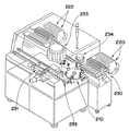
また、図25から図28に示すように、上記電子部品集合体の製造を行う電子部品集合体製造装置210を多機能型及び高速機型の部品実装装置内にそれぞれ組み込むようにしてもよい。
【0120】
すなわち、図25に示す電子部品集合体製造装置210では、モータなどの回転駆動装置204により所定角度毎に間欠的に回転可能な回転テーブル203を備え、回転テーブル203上には、複数のチップ部品1,…,1を収納可能な矩形枠型のチップ部品位置規制部材202,…,202が固定されている。この例では、回転テーブル203の間欠回転に従い、各チップ部品位置規制部材202は、チップ部品積層位置I、チップ部品位置規制位置II、絶縁シート貼り付け位置III、チップ部品固定位置IV、接着剤硬化位置V、チップ部品取出し位置VIに順に位置するようにしている。
【0121】
まず、部品積層位置Iでは、複数のチップ部品1,…,1を矩形枠型のチップ部品位置規制部材202内に吸着ノズル208を使用して積層する。矩形枠型のチップ部品位置規制部材202は、その内側のチップ部品収納空間が1個のチップ部品1の外形より若干大きく形成されており、後述する部品規制位置IIで位置規制が可能となるようにしている。この部品積層位置Iでは、最下位のチップ部品1に対しては、図13に示すように、その上面である積層面の両端部に絶縁シートなどの絶縁層2が配置された状態で、吸着ノズル208で吸着保持されてチップ部品位置規制部材202内に収納される。次いで、同様に、下から2番目のチップ部品1に対しても、その上面である積層面の両端部に絶縁シートなどの絶縁層2が配置された状態で、吸着ノズル208で吸着保持されてチップ部品位置規制部材202内に収納されて、最下位のチップ部品1上に積載される。所定数のチップ部品1,…,1が積層されると、回転テーブル203の間欠回転に従い、次のチップ部品位置規制位置IIに移動する。
【0122】
チップ部品位置規制位置IIでは、チップ部品1の幅方向と長手方向の両方に位置規制を行う。すなわち、図28に示すように、矩形枠型のチップ部品位置規制部材202は、その回転テーブル外周側の壁202eには上下方向に延びた開口202hを有している。この開口202hを貫通し、かつ、チップ部品収納空間内のチップ部品1の回転テーブル外周側の側面に当接する押圧板202dが配置されて、エアシリンダ202cにより押圧駆動されて、複数のチップ部品1,…,1が、一斉に、チップ部品位置規制部材202の回転テーブル内周側の規制壁202gに当接して位置規制されるようにしている。また、チップ部品収納空間内のチップ部品1の回転テーブル周方向の例えば反時計方向側の側面に当接する押圧板202bが配置されて、エアシリンダ202aにより押圧駆動されて、複数のチップ部品1,…,1が、一斉に、チップ部品位置規制部材202の回転テーブル周方向の時計方向側の規制壁202fに当接して位置規制されるようにしている。このようにして、複数のチップ部品1,…,1がその幅方向と長手方向の両方に位置規制が行われて揃えられると、回転テーブル203の間欠回転に従い、次の絶縁シート貼り付け位置IIIに移動する。
【0123】
絶縁シート貼り付け位置IIIでは、最上位置のチップ部品1の両方の電極22,22の上面に、テープ200に巻き取られている絶縁シート2,2を個別的に吸着ノズル201により取り出して、貼り付けて絶縁を行う。このようにして、最上位置のチップ部品1の電極22,22の絶縁が行われると、回転テーブル203の間欠回転に従い、次のチップ部品固定位置IVに移動する。
【0124】
チップ部品固定位置IVでは、チップ部品位置規制部材202の開口202h内に、上下方向沿いに積層された複数のチップ部品1,…,1の回転テーブル外周側の側面に、接着剤110を接着剤塗布装置205の塗布ノズル205aから塗布すると、回転テーブル203の間欠回転に従い、次の接着剤硬化位置Vに移動する。
【0125】
接着剤硬化位置Vでは、塗布された接着剤110を硬化装置206で加熱のたは紫外線照射して硬化させて、積層された複数のチップ部品1,…,1を互いに固着させて、電子部品集合体5を形成する。電子部品集合体5を形成すると、回転テーブル203の間欠回転に従い、次のチップ部品取出し位置VIに移動する。
【0126】
チップ部品取出し位置VIでは、チップ部品位置規制部材202内に収納された電子部品集合体5の最上面の吸着面を吸着ノズル207により吸着して、チップ部品位置規制部材202内から取り出し、90度回転させたのち、電子部品集合体5を回路基板22に実装する。チップ部品位置規制部材202内から電子部品集合体5が取り出されると、回転テーブル203の間欠回転に従い、空のチップ部品位置規制部材202がチップ部品積層位置Iに移動して、上記したように、複数のチップ部品1,…,1の積層を開始する。
【0127】
このようにして、回転テーブル203の回転に従い、複数のチップ部品1,…,1がチップ部品位置規制部材202内に積層されて電子部品集合体5が製造されて基板22に実装されていく。
【0128】
なお、チップ部品積層位置Iにおいて、絶縁シートの代わりに絶縁性接着剤を各電極の上面又は下面(ただし、最下位のチップ部品の下面が実装面の場合にはその下面を除く。)にのみ配置するようにして、接着剤が硬化しないうちにチップ部品位置規制位置IIでチップ部品の位置規制を行うようにすれば、チップ部品固定位置IVが不要となる。
【0129】
また、部品積層位置Iにおいて、1個のチップ部品1を矩形枠型のチップ部品位置規制部材202内に吸着ノズル208を使用して積層する毎に、積載されたチップ部品1の少なくとも電極上に、吸着ノズル201を使用して絶縁シート2,2を貼り付けるようにしてもよい。このようにすれば、絶縁シート貼り付け位置IIIで行う絶縁シート貼り付け動作を不要にすることができて、絶縁シート貼り付け位置IIIを省略することができる。又は、絶縁シート貼り付け位置IIIでは最上部のチップ部品1の少なくとも電極上に、吸着ノズル201を使用して絶縁シート2,2を貼り付けるようにしてもよい。
【0130】
また、部品積層位置Iにおいて、1個のチップ部品1を矩形枠型のチップ部品位置規制部材202内に吸着ノズル208を使用して積層し、押圧板202dと押圧板202bのそれぞれのエアシリンダの駆動によりチップ部品1がその幅方向と長手方向の両方に位置規制が行われて揃えたのち、積載され揃えられたチップ部品1の少なくとも電極上に、吸着ノズル201を使用して絶縁シート2,2を貼り付けるようにしてもよい。このようにすれば、チップ部品位置規制位置IIで行うチップ部品位置規制動作、及び、絶縁シート貼り付け位置IIIで行う絶縁シート貼り付け動作がそれぞれ不要になり、チップ部品位置規制位置II及び絶縁シート貼り付け位置IIIを省略することができる。又は、2つの位置II及びIIIでの両方の動作を不要にするのではなく、チップ部品位置規制位置IIでのみ、全体のチップ部品位置規制動作を行い、絶縁シート貼り付け位置IIIを省略するか、又は、絶縁シート貼り付け位置IIIでは最上部のチップ部品1の少なくとも電極上に、吸着ノズル201を使用して絶縁シート2,2を貼り付けを行い、チップ部品位置規制位置IIを省略するようにしてもよい。
【0131】
また、この装置では、上記した工程に限られるものではなく、上記各位置での装置を適宜変更して、先の実施形態において説明した図3などの電子部品集合体製造方法を行うようにしてもよい。
【0132】
図26には、上記電子部品集合体製造装置210が組み込まれた多機能型の部品実装装置を示す。
【0133】
図26において、210は上記電子部品集合体製造装置、220は多数のチップ部品が収納されて1個ずつ取り出し位置に供給可能な部品供給カセツトなどから構成されるチップ部品供給装置、221はXYテーブルなどから構成される回路基板位置決め装置、222は回路基板23に実装すべき多数の部品が収納されて1個ずつ取り出し位置に供給可能な部品供給カセツトなどから構成される部品供給装置、223は複数例えば5本の吸着ノズルを有する実装ヘッド、224は実装ヘッド223をXY方向に移動させるXYロボット、225は基板搬送装置である。よって、基板搬送装置225により搬送された基板23が回路基板位置決め装置221により位置決めされる。実装ヘッド223はXYロボット224により駆動されて、部品供給装置222に移動し、部品供給装置222から供給される複数の部品を複数の吸着ノズルで吸着保持したのち、位置や姿勢認識動作後に、回路基板位置決め装置221により位置決めされた回路基板23に実装する。また、実装ヘッド223はXYロボット224により駆動されて、電子部品集合体製造装置210に移動し、電子部品集合体製造装置210から供給される電子部品集合体を吸着ノズルで吸着保持したのち、回路基板位置決め装置221により位置決めされた回路基板23に実装する。このとき、必要に応じて、電子部品集合体を90度回転させたのち、位置決めして回路基板23に実装するようにしてもよい。このような実装動作の間、電子部品集合体製造装置210では電子部品集合体が連続的に製造され続ける。
【0134】
このような構成によれば、電子部品集合体の製造と基板への部品実装とを並行して同時的に行うことができる。
【0135】
また、図27には、上記電子部品集合体製造装置210が組み込まれた高速機型の部品実装装置を示す。
【0136】
図27において、210は上記電子部品集合体製造装置、220は多数のチップ部品が収納されて1個ずつ取り出し位置に供給可能な部品供給カセツトなどから構成されるチップ部品供給装置、231はXYテーブルなどから構成される回路基板位置決め装置、222は回路基板23に実装すべき多数の部品が収納されて1個ずつ取り出し位置に供給可能な部品供給カセツトなどから構成される部品供給装置、233は多数の吸着ノズルを間欠的に回転駆動するロータリーヘッド、234は多数の吸着ノズルを間欠的に回転駆動するチップ部品供給用ロータリーヘッド、235は基板搬送装置である。よって、基板搬送装置235により搬送された基板23が回路基板位置決め装置231により位置決めされる。ロータリーヘッド233により多数の吸着ノズルが間欠的に回転駆動される一方、ロータリーヘッド233の部品吸着位置には部品供給装置駆動装置230により所望の部品供給装置222が一軸方向に高速で進退して位置決めさせ、位置決めされた部品供給装置222から部品が供給されて当該部品をロータリーヘッド233の吸着ノズルで吸着保持したのち、ロータリーヘッド233により間欠的に回転されて、位置や姿勢認識動作後に、回路基板位置決め装置221により位置決めされた回路基板23に次々に実装する。また、ロータリーヘッド233が電子部品集合体供給位置に位置したとき、電子部品集合体製造装置210から供給される電子部品集合体をロータリーヘッド233の吸着ノズルで吸着保持したのち、位置や姿勢認識動作後に、回路基板位置決め装置231により位置決めされた回路基板23に実装する。このとき、必要に応じて、電子部品集合体を90度回転させたのち、位置決めして回路基板23に実装するようにしてもよい。このような実装動作の間、電子部品集合体製造装置210では、チップ部品供給装置220,…,220から供給されるチップ部品1,…,1をチップ部品供給用ロータリーヘッド234の間欠回転駆動により電子部品集合体製造装置210に連続的に供給して電子部品集合体が連続的に製造され続ける。
【0137】
このような構成によれば、電子部品集合体の製造と基板への部品実装とを並行して同時的に行うことができる。
【0138】
なお、上記各部品実装装置の電子部品集合体製造装置210において、電子部品集合体を実装ヘッド223又はロータリーヘッド233の吸着ノズルに供給するとき、電子部品集合体製造装置210から直接供給するものに限らず、電子部品集合体製造装置210で製造された電子部品集合体を予め製造しておき、一時的にトレーやベルトコンベヤなどの保持部材に保持するようにし、保持部材から供給される電子部品集合体を上記吸着ノズルにより吸着保持して実装するようにしてもよい。
【0139】
また、液状絶縁層を使用した電子部品集合体とシート状絶縁層を使用した電子部品集合体の組み合わせも可能である。例えば、1個のチップ部品同士の固着はシート状絶縁層で行い、そのように積層された電子部品集合体同士の固着は液状絶縁層で行うことができる。
【0140】
また、上記各実施形態では、接着層として、絶縁機能と接着機能の両方の機能を有する絶縁層を使用する場合について説明したが、これに限るものではなく、上記接着層は、上記積層された電子部品の上記積層面の互いに対向する電極に配置されて上記積層された電子部品の上記積層面の互いに対向する電極間を絶縁する絶縁層と、上記積層された電子部品同士を固着させる接着剤とを備えるように構成してもよい。すなわち、図29に示すように、上記接着層を構成する上記絶縁層の一例として機能する一枚の粘着性絶縁シート103を隣接するチップ部品1,1の電極22,22間に配置して絶縁層を構成したのち、図31に示すように、上記接着層を構成する上記接着剤の一例として機能する絶縁性の無い接着剤105でチップ部品1,1を互いに固着するようにしてもよい。このとき、好ましくは、一枚の粘着性絶縁シート103及び接着剤105に、チップ部品1,1の電極22,22以外の部分を露出させるための空間を形成するのが好ましい。
【0141】
また、この場合、隣接するチップ部品1,1の電極22,22の両方に一枚の粘着性絶縁シート103をそれぞれ配置するものに限らず、図32に示すように、いずれか一方の電極22に対してのみ一枚の粘着性絶縁シート103を配置するようにしてもよい。また、一枚の粘着性絶縁シート103で両端部の電極22,22を絶縁させるものに限らず、図30に示すように、2枚の粘着性絶縁シート103で両端部の電極22,22をそれぞれ絶縁させるようにしてもよい。
【0142】
上記接着剤又は接着層の特性として高強度が必要な場合には、80kgf/cm2以上とし、電気絶縁が必要な場合には、1×1010Ω以上とし、低吸水が必要な場合には、50wt%以上とする。
【0143】
また、接着剤又は接着層の材質としては、モノマーとして、エポキシ系、ビスフェノールA、ビスフェノールF、アミノフェノール型、フェトルノボラック型があり、硬化剤としては、イミダゾール系、アミン系、アミンアダクト系、ヒトラジン系、イソシアネート系があり、フィラーとしては、シリカ、アルミナ、タルク、フッ化ホウソ、マイカがあり、これらのモノマー、硬化剤、及び、フィラーの中では、任意のものを選択して適宜組合わせることができる。また、他の接着剤又は接着層として、モノマーとして脂環式、硬化剤として酸無水物系、及び、フィラーとしてウィスカー又は窒化アルミを組み合わせて使用することができる。接着剤又は接着層の1つの実施例としては、ビスフェノールA型エポキシが100重量部、2−ミチルイミダゾールアジンが7重量部、シリカ(SiO2)が20重量部とする。
【0144】
また、各チップ部品1において、絶縁すべき電極の面は、少なくとも積層される積層面に位置する電極の面であり、さらに好ましくは、実装時に露出して他の部品との電気的接触を防止する必要がある電極面も絶縁するようにしたほうが電気的安定性の観点から好ましい。
【0145】
【実施例】
以下に、本発明の上記第1及び第2実施形態にかかる電子部品集合体及びその実装方法の具体的な実施例を挙げる。
<実施例1〜実施例4>
チップ部品間の絶縁材料として、以下の樹脂を用いた。
【0146】
シート状絶縁層としては、エポキシ系樹脂(膜厚=50μm、日東電工社製)を使用した。
【0147】
ペースト(液状絶縁層)としては、エポキシ系樹脂(油化シェルエポキシ社製)を使用した。
【0148】
そして、上記絶縁材料と10個のチップ部品(寸法:1.0mm×0.5mm×0.25mm)とを用いて、電子部品集合体をそれぞれ作製し、回路基板上に実装したサンプルを作製した(実施例1〜実施例4)。
【0149】
実施例1は図13の電子部品集合体3に対応し、実施例2は図1の電子部品集合体5に対応し、実施例3は図19(C)の電子部品集合体7に対応し、実施例4は図12(C)の電子部品集合体8に対応する。
<比較例1>
比較例1として、図21に示すように、回路基板上の隣接するチップ部品10(寸法:1.0mm×0.5mm×0.2mm)間の距離を0.3mmとして10個実装したサンプルを作製した。なお、図21において、参照符号11は回路基板上の基板電極、12は回路基板上での10個のチップ部品10,…,10の実装面積である。
【0150】
上記のようにして得られた実装サンプルについて各種特性を測定した。その測定方法は以下の通りである。
【0151】
1)実装面積:作製した実装サンプルの基板電極を含む回路基板の実装面積(例えば図21では基板電極11を含む回路基板の実装面積12)を測定した。
【0152】
2)部品ズレ率:自動電子部品実装装置(図示せず)にて、部品実装後にチップ部品が基板電極から0.1mm以上離れている部品数(n)を測定し、(n/10)×100(%)を部品ズレ率とした。
【0153】
3)部品実装時間:実装速=0.1秒/1個の自動電子部品実装機(図示せず)にてチップ部品を回路基板上に実装した際に要した時間を測定した。
【0154】
各サンプルの特性測定結果を表1に示す。
【0155】
【表1】

表1より、本発明の実施形態の実施例による電子部品集合体及びその実装方法は、チップ部品の実装面積が小さく、実装されたチップ部品がズレることなく、またチップ部品の実装時間が短いという結果が得られた。
【0157】
【発明の効果】
本発明の電子部品集合体及びその実装方法によれば、電子部品の位置ズレ不良を引き起こすことなく、回路基板などの被実装体への電子部品の実装面積を小さくし、実装時間を大幅に短縮することができる。
【0158】
すなわち、本発明の電子部品集合体及びその実装方法によれば、複数の電子部品をそれぞれ個別に回路基板などの被実装体に実装するのではなく、複数の電子部品を互いに長手方向と直交する方向に、かつ、横方向に積層し、かつ、隣接電子部品の電極間には絶縁層を配置して隣接電子部品を互いに固着して電子部品集合体を構成しているため、複数の電子部品間の位置ズレを防止することができ、かつ、実装面積を小さくすることができる。
【0159】
また、本発明の電子部品集合体によれば、隣接電子部品の電極間には絶縁層を配置し、隣接電子部品の電極以外の部分には絶縁層がなく、放熱用空間が確保できるため、電子部品の発熱時に放熱作用を行わせることができる。
【0160】
また、本発明の電子部品集合体及びその実装方法によれば、複数個の電子部品で構成される電子部品集合体を1つの部品として取り扱うことにより回路基板などに実装することができるため、複数個の電子部品をそれぞれ実装する場合と比較して、実装工程に要する時間が短縮できる。
【0161】
また、本発明の電子部品集合体及びその製造方法によれば、電子部品集合体を部品収納部材に収納するとき、上下方向に2個の積層された電子部品より構成する電子部品集合体を90度回転させて横方向に積層された状態として、電子部品集合体の実装時に電子部品集合体の吸着面を上面に向くようにしたのち、その状態で部品収納部材に収納するようにすれば、電子部品集合体の実装時に部品収納部材内の電子部品集合体の吸着面を吸着ノズルで吸着すれば、電子部品集合体の全ての電極を回路基板に対向させることができ、従来の実装方法のまま、狭隣接実装が可能になる。また、電子部品集合体を回路基板などに実装するときに電子部品集合体を90度回転させようとすると実装ヘッドの構造が複雑化するが、上記したように、部品収納部材に収納するときに予め90度回転させて吸着面が上向きになるようにすれば、実装時に電子部品集合体を90度回転させる必要がなくなり、実装ヘッドの構造を複雑化させることがない。
【0162】
また、電子部品を吸着ノズルで吸着するとき、吸着ノズルは外径が小さくなるほど製作が困難であり、かつ、ゴミ等の影響を受けやすくなるので小さくするのは現実的に困難であるため、従来の実装状態のように1個の電子部品の幅より吸着ノズルの外径が大きいためはみ出てしまう部分がある。このような状態で電子部品を吸着ノズルで吸着したのち回路基板などに実装すると、吸着ノズルのはみ出した部分が、既に回路基板に実装されている他の部品に当らないようにする必要があり、電子部品を狭隣接ピッチで実装するのに一番問題となる点である。
【0163】
これに対して、本発明の電子部品集合体及びその実装方法では、電子部品が積層されて構成された電子部品集合体の実装は、電子部品集合体において電子部品自体が既に狭隣接ピッチに配置され、かつ、固着されてる上に、吸着ノズルにより吸着可能な吸着面を1個の電子部品の幅より大きく、具体的には、複数個の電子部品の幅まで大きくすることができるので、実装動作が安定して行える。また、吸着ノズルと既に実装された他の部品との接触が無くなる為、電子部品同士の狭隣接ピッチでの実装が可能になる。
【図面の簡単な説明】
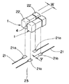
【図1】 (A),(B)はそれぞれ本発明の第1実施形態にかかる電子部品集合体及び電子部品集合体の実装方法において、電子部品集合体の製造方法を示す工程図及び電子部品集合体の実装方法により電子部品集合体を回路基板に実装した状態の斜視図である。
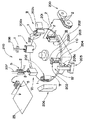
【図2】 上記第1実施形態の電子部品集合体の製造方法を実施することができるチップ部品積層装置の透視的な概略斜視図である。
【図3】 上記電子部品集合体の製造方法のフローチャートである。
【図4】 上記電子部品集合体の製造方法においてチップ部品に接着剤を塗布する状態の説明図である。
【図5】 上記電子部品集合体の製造方法においてチップ部品を積層する状態の説明図である。
【図6】 上記電子部品集合体の製造方法においてチップ部品を90度回転させる状態の説明図である。
【図7】 上記電子部品集合体の製造方法において電子部品集合体を吸着ノズルで吸着する状態の説明図である。
【図8】 (A),(B)はそれぞれ上記電子部品集合体の製造方法において3個のチップ部品を積層する状態の説明図及び積層された2個チップ部品の上に、積層された2個チップ部品を積層する状態の説明図である。
【図9】 上記電子部品集合体の製造方法においてマーク付き積層チップ部品の斜視図である。
【図10】 上記電子部品集合体の製造方法において一対の規正部材の規制によりチップ部品の位置決めを行う状態を示す説明図である。
【図11】 (A),(B)はそれぞれ上記電子部品集合体の製造方法において複数個のチップ部品1,…,1の積層を同時的に、かつ、連続的に行う場合を示す説明図である。
【図12】 (A),(B),(C)はそれぞれ本発明の第1実施形態の変形例にかかる電子部品集合体及び電子部品集合体の実装方法において、電子部品集合体の製造方法を示す工程図及び電子部品集合体の実装方法により電子部品集合体を回路基板に実装した状態の斜視図である。
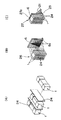
【図13】 (A),(B)はそれぞれ本発明の第2実施形態にかかる電子部品集合体及び電子部品集合体の実装方法において、電子部品集合体の製造方法を示す工程図及び電子部品集合体の実装方法により電子部品集合体を回路基板に実装した状態の斜視図である。
【図14】 本発明の第2実施形態にかかる電子部品集合体及び電子部品集合体の実装方法のフローチャートである。
【図15】 (A),(B)はそれぞれチップ部品にシート状絶縁層を溶着する状態の説明図及び溶着後の電子部品の説明図である。
【図16】 (A),(B)はそれぞれチップ部品に粘着層を転写する状態の説明図及び転写後の電子部品の説明図である。
【図17】 チップ部品の電極の幅とランドの幅との関係を示す説明図である。
【図18】 (A),(B)はそれぞれ本発明の第1実施形態にかかる電子部品集合体を吸着ノズルで吸着して実装する状態の説明図及び従来の実装方法においてチップ部品を1個ずつ吸着ノズルで吸着して実装する状態の説明図である。
【図19】 (A),(B),(C)はそれぞれ本発明の第2実施形態の変形例にかかる電子部品集合体及び電子部品集合体の実装方法において、電子部品集合体の製造方法を示す工程図及び電子部品集合体の実装方法により電子部品集合体を回路基板に実装した状態の斜視図である。
【図20】 (A),(B),(C)はそれぞれ本発明の第2実施形態の別の変形例にかかる電子部品集合体及び電子部品集合体の実装方法において、電子部品集合体の製造方法を示す工程図及び電子部品集合体の実装方法により電子部品集合体を回路基板に実装した状態の斜視図である。
【図21】 従来のチップ部品の回路基板への実装状態を示す平面図である。
【図22】 図1の本発明の第1実施形態の別の変形例として、絶縁シートを介して2個の電子部品集合体を連結して1つの電子部品集合体として実装する状態を説明する斜視図である。
【図23】 図12の本発明の第1実施形態のさらに別の変形例として、絶縁シートを介して2個の電子部品集合体を連結して1つの電子部品集合体として実装する状態を説明する斜視図である。
【図24】 図23の電子部品集合体を絶縁シートを介してさらに別の図23の電子部品集合体と連結して、1つの電子部品集合体として実装する状態を説明する斜視図である。
【図25】 本発明の他の実施形態として電子部品集合体を製造する装置を示す斜視図である。
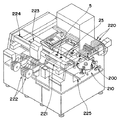
【図26】 図25の電子部品集合体製造装置が組み込まれた多機能型の部品実装装置の部分的に透視図的に示された概略斜視図である。
【図27】 図25の電子部品集合体製造装置が組み込まれた高速機型の部品実装装置の部分的に透視図的に示された概略斜視図である。
【図28】 図25の電子部品集合体製造装置のチップ部品位置規制部材の拡大平面図である。
【図29】 上記実施形態において、一枚の絶縁層を隣接するチップ部品間に配置して互いに絶縁層の有する粘着性でもってチップ部品を固着する変形例を示す説明図である。
【図30】 上記実施形態において、2枚の絶縁層を隣接するチップ部品の電極間に配置して互いに絶縁層の有する粘着性でもってチップ部品を固着する変形例を示す説明図である。
【図31】 図30の変形例において対向電極間に2枚の絶縁層を配置する状態の電極間部分の拡大図である。
【図32】 図30の変形例において対向電極間に1枚の絶縁層を配置する状態の電極間部分の拡大図である。
【符号の説明】
1…チップ部品、2…絶縁層、3,5,7,8…電子部品集合体、3a,5a…吸着面、4…絶縁性接着剤、5a…吸着面、6…補助シート、6a…回路配線、7a,8a…吸着面、21…回路、22…チップ部品電極、23…回路基板、24…絶縁層、26,27…電子部品集合体、27a…吸着面、29…放熱用空間、30…送りリール、31…巻取リール、32…加熱加圧ツール、32a…加圧部、33…絶縁性粘着フィルム、34…ベースフィルム、35…粘着層、36…加圧ツール、40…マーク、41,42…規制部材、41a,42a…規制縁部、41b,42b…係止突起、43…隙間、44…規制板、45…隙間、68…XYロボット、69…吸着ノズル、70…部品供給部、70a…部品供給カセット、71…吸着ヘッド、72…絶縁性接着剤塗布装置、72a…塗布ノズル、73…認識装置、74…Y方向移動装置、75…X方向移動装置、76…Y方向駆動モータ、77…X方向駆動モータ、78…チップ部品載置テーブル、78a…吸引孔、79…チップ部品認識装置、80…モータ、81…Y方向移動装置、81a…Y方向移動装置本体、82…ネジ軸、83…電子部品集合体収納部、83a…部品収納カセット、84…硬化装置、85…実装装置出入り口、90…吸着ブロック、90a…吸着面、100,101,102,103…絶縁シート、105…接着剤、200…テープ、201…吸着ノズル、202…矩形枠型のチップ部品位置規制部材、202a…エアシリンダ、202b…押圧板、202c…エアシリンダ、202d…押圧板、202f…回転テーブル周方向の時計方向側の規制壁、202g…回転テーブル内周側の規制壁、202h…開口、203…回転テーブル、204…回転駆動装置、205…接着剤塗布装置、205a…塗布ノズル、206…硬化装置、207…吸着ノズル、208…吸着ノズル、210…電子部品集合体製造装置、220…チップ部品供給装置、221…回路基板位置決め装置、222…部品部品供給装置、223…実装ヘッド、224…XYロボット、225…基板搬送装置、230…部品供給装置駆動装置、231…基板位置決め装置、233…ロータリーヘッド、234…チップ部品供給用ロータリーヘッド、235…基板搬送装置、I…チップ部品積層位置、II…チップ部品位置規制位置、III…絶縁シート貼り付け位置、IV…チップ部品固定位置、V…接着剤硬化位置、VI…チップ部品取出し位置。[0001]
BACKGROUND OF THE INVENTION
The present invention relates to an electronic component assembly in which a plurality of rectangular parallelepiped electronic components (hereinafter simply referred to as chip components) having electrodes at both ends, a method of manufacturing the electronic component assembly, a circuit board, and the like The present invention relates to a mounting method for an electronic component assembly in which the electronic component assembly is mounted on a mounted body such as a circuit forming body or other components.
[0002]
[Prior art]
In recent years, as a method for reducing the mounting area of a chip component on a circuit board, it is common to reduce the distance between adjacent chip components.
[0003]
[Problems to be solved by the invention]
However, when the distance between the chip components is reduced, the chip component to be mounted in the chip component mounting process is already mounted if the chip component is sucked and mounted while being slightly displaced from the suction nozzle. In addition, there is a problem that physical contact with other chip parts causes a misalignment of the chip parts. Also, when recovering, for example, remounting a short component, the short component could not be mounted next to the tall component. Further, when the number of chip parts to be mounted is increased, there is a problem in the mounting process in that the time required for mounting is extended in a geometric series. In addition, there is a problem that if the chip component is physically contacted and mounted in order to reduce the distance between the chip components in this way, the heat radiation action cannot be performed when the chip component generates heat. It was.
[0004]
Accordingly, an object of the present invention is to solve the above-described problem, and can reduce the mounting area of the electronic component on the mounted body without causing a misalignment of the electronic component, and the electronic component. Provided are an electronic component assembly capable of radiating heat when heat is generated, a method of manufacturing the electronic component assembly, and a mounting method of the electronic component assembly capable of manufacturing an excellent quality mounted body. It is in.
[0005]
[Means for Solving the Problems]
In order to achieve the above object, the present invention is configured as follows.
[0006]
According to the first aspect of the present invention,Both endsAt least two or more rectangular parallelepiped electronic components having electrodes are stacked in a direction perpendicular to the longitudinal direction of the electronic components, and the stacked electronic components face each other.The electrodes are fixed with an adhesive insulating layer, and a space for heat dissipation is formed between the stacked surfaces of electronic components other than the electrodes facing each other.Electronic component assemblyIs a mounting method of an electronic component assembly that is mounted at a predetermined position on a circuit board after being sucked by a suction nozzle,
The suction surface of the electronic component assembly sucked by the suction nozzle is a side surface in the longitudinal direction of the stacked electronic components that straddle a plurality of adjacent electronic components, and the plurality of adjacent electronic components It is a side other than the electrode,
An electronic component assembly mounting method is provided, wherein an outer diameter of the suction nozzle is larger than a width in a direction perpendicular to a longitudinal direction of one electronic component.
[0007]
According to a second aspect of the invention,An outer diameter of the suction nozzle is larger than a width in a direction orthogonal to a longitudinal direction of the plurality of electronic components.Electronic component assembly according to the first aspectHow to implementI will provide a.
[0028]
DETAILED DESCRIPTION OF THE INVENTION
Embodiments according to the present invention will be described below in detail with reference to the drawings.
[0029]
The
[0030]
As shown in FIG. 1A, the
[0031]
The
[0032]
As shown in FIG. 1B, the
[0033]
The side surface of the at least one
[0034]
A method for mounting the electronic component assembly for mounting the
[0035]
First, an electronic component assembly mounting apparatus, that is, a chip component stacking apparatus that can implement the mounting method will be described with reference to FIG. In this mounting apparatus, a Y-
[0036]
In the
[0037]
The table 78 penetrates and forms one or more suction holes 78a,..., 78a connected to a vacuum suction device (not shown) so that the
[0038]
The
[0039]
The
[0040]
The electronic component
[0041]
The electronic component assembly mounting apparatus configured as described above conveys five
[0042]
First, as shown in FIG. 5, in step S <b> 11, one
[0043]
Next, in step S12, the
[0044]
Next, in step S <b> 13, the
[0045]
Next, in step S <b> 14, the
[0046]
Next, in step S15, based on the recognition result by the
[0047]
Next, in step S <b> 16, the
[0048]
Next, in step S17, the
[0049]
Note that step S15, step S16, and step S17 may be performed simultaneously by arranging necessary devices or members, respectively.
[0050]
Next, in step S18, the
[0051]
Next, in step S19, as shown in FIG. 5, the
[0052]
Next, in step S20, the adhesive insulating
[0053]
Next, in step S21, it is determined whether there is a
[0054]
Next, in step S <b> 22, the side surfaces of the two stacked
[0055]
Next, in step S23, the
[0056]
Next, in step S24, the suction surface 5a of the
[0057]
Next, in step S25, the chip
[0058]
Next, in step S <b> 26, the
[0059]
In this way, the
[0060]
When the
[0061]
Further, since the
[0062]
When mounting the
[0063]
According to the first embodiment, the plurality of
[0064]
Further, when the
[0065]
In addition, since the
[0066]
Further, if the
[0067]
Further, the
[0068]
On the other hand, in the first embodiment, as shown in FIG. 18A, mounting of the
[0069]
In addition, this invention is not limited to the said embodiment, It can implement with another various aspect.
[0070]
For example, as shown in FIG. 9, when the stacking
[0071]
In the first embodiment, the recognition operation is frequently used in order to stack the
[0072]
In this way, by restricting the position of the
[0073]
In addition, the
[0074]
As a modification of the first embodiment, the
[0075]
The material used as the
[0076]
When considering a method of reducing the mounting area of the circuit board by shortening the distance between adjacent chip components mounted independently, the direction is limited to the direction along the surface of the circuit board. On the other hand, in the carrier-type
[0077]
Further, the insulating layer is not limited to a liquid layer, and may be a sheet as described below. That is, the
[0078]
As shown in FIG. 13A, the
[0079]
The insulating
[0080]
A side surface of the at least one
[0081]
As shown in FIG. 13B, the
[0082]
FIG. 14 is a flowchart showing a method of manufacturing the
[0083]
First, as shown in FIG. 14, in step S31, one
[0084]
Next, in step S32, the
[0085]
Next, in step S <b> 33, the
[0086]
Next, in step S34, the sheet-like insulating
[0087]
Next, in S35, the
[0088]
Next, in S36, the
[0089]
Next, in S37, the
[0090]
Next, in S38, the
[0091]
Next, in S39, the electrodes of the
[0092]
Next, in S40, it is determined whether there is a
[0093]
Next, in S41, the side surfaces of the two stacked
[0094]
Next, in S42, the
[0095]
Next, in S43, the suction surface 3a of the
[0096]
Next, in S44, the bottom of the
[0097]
Next, in S45, the
[0098]
In this way, the
[0099]
When the
[0100]
Further, since the
[0101]
According to the second embodiment, the plurality of
[0102]
Further, when the
[0103]
Further, since the
[0104]
Also, if the
[0105]
Further, the
[0106]
On the other hand, in the second embodiment, as shown in FIG. 18A, mounting of the
[0107]
In the second embodiment, as a specific example of joining the
[0108]
As another specific example, as shown in FIG. 16, an
[0109]
As a modification of the second embodiment, the
[0110]
The material used as the
[0111]
Conventionally, a method for reducing the mounting area of a circuit board by reducing the distance between adjacent chip components that are independently mounted has been limited to the direction along the surface of the circuit board. On the other hand, in the electronic component assembly 7 of the modified example of the second embodiment, the plurality of
[0112]
Further, as another modification of the second embodiment, the
[0113]
The material used as the
[0114]
Conventionally, a method for reducing the mounting area of a circuit board by reducing the distance between adjacent chip components that are independently mounted has been limited to the direction along the surface of the circuit board. On the other hand, in the
[0115]
In each of the embodiments described above, the chip components constituting the electronic component assembly may be different types of resistors, capacitors, etc., their capacities, and external dimensions (not shown), and the number of chip components is 2 If it is more than one, no upper limit is required.
[0116]
Moreover, as shown in FIG. 22 as another modification of 1st Embodiment of this invention of FIG. 1, not only what uses the electronic component aggregate |
[0117]
In addition, as shown in FIG. 23, as another modification of the first embodiment of the present invention shown in FIG. 12, the adhesive property is not limited to the
[0118]
In addition, the adhesive is applied to one side surface of the plurality of stacked
[0119]
Further, as shown in FIGS. 25 to 28, an electronic component
[0120]
That is, the electronic component
[0121]
First, at the component stacking position I, a plurality of
[0122]
In the chip part position restriction position II, the position restriction is performed in both the width direction and the longitudinal direction of the
[0123]
At the insulating sheet attaching position III, the insulating
[0124]
At the chip component fixing position IV, the adhesive 110 is applied to the side surface on the outer peripheral side of the rotary table of the plurality of
[0125]
At the adhesive curing position V, the applied adhesive 110 is cured by heating or irradiating with ultraviolet light with the
[0126]
At the chip component take-out position VI, the uppermost suction surface of the
[0127]
In this way, according to the rotation of the
[0128]
At the chip component stacking position I, instead of the insulating sheet, an insulating adhesive is applied only to the upper or lower surface of each electrode (however, when the lowermost chip component is the mounting surface, the lower surface is excluded). If the chip component position is regulated at the chip component position regulating position II before the adhesive is cured, the chip component fixing position IV becomes unnecessary.
[0129]
Further, at the component stacking position I, every time one
[0130]
Further, at the component stacking position I, one
[0131]
In addition, this apparatus is not limited to the above-described process, and the apparatus at each position described above is appropriately changed to perform the electronic component assembly manufacturing method such as FIG. 3 described in the previous embodiment. Also good.
[0132]
FIG. 26 shows a multifunctional component mounting apparatus in which the electronic component
[0133]
In FIG. 26, 210 is an electronic component assembly manufacturing apparatus, 220 is a chip component supply apparatus configured by a component supply cassette or the like in which a large number of chip components are stored and can be supplied one by one to an extraction position, and 221 is an XY table. A circuit
[0134]
According to such a configuration, the manufacture of the electronic component assembly and the component mounting on the substrate can be performed simultaneously in parallel.
[0135]
FIG. 27 shows a high-speed type component mounting apparatus in which the electronic component
[0136]
In FIG. 27, 210 is an electronic component assembly manufacturing apparatus, 220 is a chip component supply apparatus configured by a component supply cassette or the like in which a large number of chip components are stored and can be supplied one by one to an extraction position, and 231 is an XY table. The circuit
[0137]
According to such a configuration, the manufacture of the electronic component assembly and the component mounting on the substrate can be performed simultaneously in parallel.
[0138]
In the electronic component
[0139]
Also, a combination of an electronic component assembly using a liquid insulating layer and an electronic component assembly using a sheet-like insulating layer is possible. For example, one chip component can be fixed with a sheet-like insulating layer, and the electronic component assemblies thus stacked can be fixed with a liquid insulating layer.
[0140]
In each of the above embodiments, the case where an insulating layer having both an insulating function and an adhesive function is used as the adhesive layer has been described. However, the present invention is not limited to this, and the adhesive layer is laminated as described above. An insulating layer that is disposed on the electrodes facing each other on the laminated surface of the electronic component and insulates the electrodes facing each other on the laminated surface of the laminated electronic component, and an adhesive that fixes the laminated electronic components together You may comprise so that. That is, as shown in FIG. 29, one adhesive insulating
[0141]
Further, in this case, not only one adhesive insulating
[0142]
When high strength is required as a property of the adhesive or adhesive layer, 80 kgf /
[0143]
The material of the adhesive or the adhesive layer includes, as a monomer, an epoxy type, bisphenol A, bisphenol F, aminophenol type, fetor novolac type, and as a curing agent, an imidazole type, an amine type, an amine adduct type, There are human-razine-based and isocyanate-based, and fillers include silica, alumina, talc, boron fluoride, and mica. Among these monomers, curing agents, and fillers, any one can be selected and combined as appropriate. be able to. Further, as another adhesive or adhesive layer, an alicyclic monomer can be used, an acid anhydride system can be used as a curing agent, and whisker or aluminum nitride can be used in combination as a filler. As one example of the adhesive or adhesive layer, bisphenol A type epoxy is 100 parts by weight, 2-mitylimidazole azine is 7 parts by weight, silica (SiO 22) Is 20 parts by weight.
[0144]
Further, in each
[0145]
【Example】
Specific examples of the electronic component assembly and the mounting method according to the first and second embodiments of the present invention will be given below.
<Example 1 to Example 4>
The following resins were used as insulating materials between chip components.
[0146]
As the sheet-like insulating layer, an epoxy resin (film thickness = 50 μm, manufactured by Nitto Denko Corporation) was used.
[0147]
As the paste (liquid insulating layer), an epoxy resin (manufactured by Yuka Shell Epoxy Co., Ltd.) was used.
[0148]
Then, using the insulating material and 10 chip components (dimensions: 1.0 mm × 0.5 mm × 0.25 mm), an electronic component assembly was prepared, and a sample mounted on a circuit board was prepared. (Examples 1 to 4).
[0149]
Example 1 corresponds to the
<Comparative Example 1>
As Comparative Example 1, as shown in FIG. 21, 10 samples mounted with a distance of 0.3 mm between adjacent chip components 10 (dimensions: 1.0 mm × 0.5 mm × 0.2 mm) on a circuit board were mounted. Produced. 21,
[0150]
Various characteristics of the mounting sample obtained as described above were measured. The measuring method is as follows.
[0151]
1) Mounting area: The mounting area of the circuit board including the substrate electrode of the manufactured mounting sample (for example, the mounting
[0152]
2) Component deviation rate: With an automatic electronic component mounting apparatus (not shown), the number (n) of components where the chip component is 0.1 mm or more away from the substrate electrode after component mounting is measured, and (n / 10) × 100 (%) was defined as the component deviation rate.
[0153]
3) Component mounting time: mounting speed = 0.1 sec / time was measured when a chip component was mounted on a circuit board with an automatic electronic component mounting machine (not shown).
[0154]
Table 1 shows the characteristic measurement results of each sample.
[0155]
[Table 1]
From Table 1, the electronic component assembly according to the embodiment of the present invention and the mounting method thereof have a small chip component mounting area, the mounted chip component is not displaced, and the chip component mounting time is short. Results were obtained.
[0157]
【The invention's effect】
According to the electronic component assembly and the mounting method thereof of the present invention, the mounting area of the electronic component on the mounted body such as a circuit board is reduced and the mounting time is significantly shortened without causing the positional misalignment of the electronic component. can do.
[0158]
That is, according to the electronic component assembly and the mounting method of the present invention, the plurality of electronic components are not individually mounted on the mounted body such as a circuit board, but the plurality of electronic components are orthogonal to each other in the longitudinal direction. A plurality of electronic components are stacked in the horizontal direction and laterally, and an insulating layer is disposed between the electrodes of adjacent electronic components so that the adjacent electronic components are fixed to each other to form an electronic component assembly. It is possible to prevent misalignment between them and to reduce the mounting area.
[0159]
In addition, according to the electronic component assembly of the present invention, an insulating layer is disposed between the electrodes of the adjacent electronic components, and there is no insulating layer in a portion other than the electrodes of the adjacent electronic components, and a space for heat dissipation can be secured. Heat dissipation can be performed when the electronic component generates heat.
[0160]
In addition, according to the electronic component assembly and the mounting method thereof of the present invention, the electronic component assembly composed of a plurality of electronic components can be mounted on a circuit board or the like by handling it as one component. Compared with the case of mounting individual electronic components, the time required for the mounting process can be shortened.
[0161]
In addition, according to the electronic component assembly and the method of manufacturing the same according to the present invention, when the electronic component assembly is stored in the component storage member, the electronic component assembly configured by two stacked electronic components in the vertical direction is provided. When the electronic component assembly is mounted in the state after being rotated in the horizontal direction, the electronic component assembly adsorbing surface is directed to the upper surface when the electronic component assembly is mounted. If the suction surface of the electronic component assembly in the component storage member is sucked by the suction nozzle when mounting the electronic component assembly, all the electrodes of the electronic component assembly can be made to face the circuit board. Narrowly adjacent mounting is possible. Also, if the electronic component assembly is rotated 90 degrees when the electronic component assembly is mounted on a circuit board or the like, the structure of the mounting head becomes complicated. However, as described above, when the electronic component assembly is stored in the component storage member If the suction surface is turned up by 90 degrees in advance, it is not necessary to rotate the electronic component assembly by 90 degrees during mounting, and the structure of the mounting head is not complicated.
[0162]
In addition, when sucking electronic components with a suction nozzle, the suction nozzle is more difficult to manufacture as the outer diameter becomes smaller, and it is more difficult to make it smaller because it is more susceptible to dust and the like. As in the mounting state, there is a portion that protrudes because the outer diameter of the suction nozzle is larger than the width of one electronic component. In such a state, when the electronic component is sucked by the suction nozzle and then mounted on the circuit board or the like, it is necessary to prevent the protruding portion of the suction nozzle from hitting other parts already mounted on the circuit board. This is the most problematic point for mounting electronic components at a narrow adjacent pitch.
[0163]
On the other hand, in the electronic component assembly and the mounting method thereof according to the present invention, the mounting of the electronic component assembly formed by stacking the electronic components is already arranged at a narrow adjacent pitch in the electronic component assembly. In addition to being fixed, the suction surface that can be sucked by the suction nozzle can be made larger than the width of one electronic component, specifically, up to the width of multiple electronic components. Operation can be performed stably. In addition, since there is no contact between the suction nozzle and other components already mounted, the electronic components can be mounted at a narrow adjacent pitch.
[Brief description of the drawings]
FIGS. 1A and 1B are a process diagram and an electronic component showing a method of manufacturing an electronic component assembly in the electronic component assembly and the electronic component assembly mounting method according to the first embodiment of the present invention, respectively. It is a perspective view of the state which mounted the electronic component assembly on the circuit board by the assembly mounting method.
FIG. 2 is a perspective schematic perspective view of a chip component laminating apparatus that can implement the method of manufacturing an electronic component assembly according to the first embodiment.
FIG. 3 is a flowchart of a manufacturing method of the electronic component assembly.
FIG. 4 is an explanatory diagram of a state in which an adhesive is applied to a chip component in the method for manufacturing an electronic component assembly.
FIG. 5 is an explanatory diagram of a state in which chip components are stacked in the method for manufacturing an electronic component assembly.
FIG. 6 is an explanatory diagram of a state in which the chip component is rotated 90 degrees in the method of manufacturing the electronic component assembly.
FIG. 7 is an explanatory diagram of a state in which the electronic component assembly is adsorbed by an adsorption nozzle in the electronic component assembly manufacturing method.
FIGS. 8A and 8B are explanatory views showing a state in which three chip components are stacked in the method for manufacturing an electronic component assembly, and two stacked on two stacked chip components, respectively. It is explanatory drawing of the state which laminates | stacks an individual chip component.
FIG. 9 is a perspective view of a laminated chip component with a mark in the manufacturing method of the electronic component assembly.
FIG. 10 is an explanatory view showing a state where the chip component is positioned by the restriction of the pair of regulating members in the method of manufacturing the electronic component assembly.
FIGS. 11A and 11B are explanatory views showing a case where a plurality of
FIGS. 12A, 12B, and 12C are an electronic component assembly and an electronic component assembly manufacturing method according to a modification of the first embodiment of the present invention, respectively. FIG. 6 is a perspective view of a state in which the electronic component assembly is mounted on the circuit board by the process diagram illustrating the electronic component assembly mounting method.
FIGS. 13A and 13B are a process diagram and an electronic component showing a method of manufacturing the electronic component assembly in the electronic component assembly and the electronic component assembly mounting method according to the second embodiment of the present invention, respectively. It is a perspective view of the state which mounted the electronic component assembly on the circuit board by the assembly mounting method.
FIG. 14 is a flowchart of an electronic component assembly and an electronic component assembly mounting method according to the second embodiment of the present invention.
FIGS. 15A and 15B are an explanatory diagram of a state in which a sheet-like insulating layer is welded to a chip component and an explanatory diagram of an electronic component after welding, respectively.
FIGS. 16A and 16B are an explanatory diagram of a state where an adhesive layer is transferred to a chip component and an explanatory diagram of an electronic component after transfer, respectively.
FIG. 17 is an explanatory diagram showing the relationship between the width of an electrode of a chip component and the width of a land.
FIGS. 18A and 18B are an explanatory diagram of a state in which the electronic component assembly according to the first embodiment of the present invention is sucked and mounted by a suction nozzle and one chip component in the conventional mounting method, respectively. It is explanatory drawing of the state mounted and picked up by a suction nozzle one by one.
FIGS. 19A, 19B, and 19C are an electronic component assembly and an electronic component assembly manufacturing method according to a modification of the second embodiment of the present invention, respectively. FIG. 6 is a perspective view of a state in which the electronic component assembly is mounted on the circuit board by the process diagram illustrating the electronic component assembly mounting method.
FIGS. 20A, 20B, and 20C are respectively an electronic component assembly and an electronic component assembly mounting method according to another modification of the second embodiment of the present invention. It is a perspective view in the state where the electronic component assembly was mounted on the circuit board by the process diagram showing the manufacturing method and the mounting method of the electronic component assembly.
FIG. 21 is a plan view showing a state in which a conventional chip component is mounted on a circuit board.
FIG. 22 illustrates a state in which two electronic component assemblies are connected via an insulating sheet and mounted as one electronic component assembly as another modification of the first embodiment of the present invention shown in FIG. It is a perspective view.
FIG. 23 illustrates a state in which two electronic component assemblies are connected via an insulating sheet and mounted as one electronic component assembly as still another modification of the first embodiment of the present invention shown in FIG. FIG.
24 is a perspective view illustrating a state in which the electronic component assembly of FIG. 23 is connected to another electronic component assembly of FIG. 23 via an insulating sheet and mounted as one electronic component assembly.
FIG. 25 is a perspective view showing an apparatus for manufacturing an electronic component assembly as another embodiment of the present invention.
26 is a schematic perspective view partially shown in a perspective view of a multi-functional component mounting apparatus in which the electronic component assembly manufacturing apparatus of FIG. 25 is incorporated.
27 is a schematic perspective view partially shown in a perspective view of a high-speed type component mounting apparatus in which the electronic component assembly manufacturing apparatus of FIG. 25 is incorporated.
28 is an enlarged plan view of a chip part position restricting member of the electronic part assembly manufacturing apparatus of FIG. 25. FIG.
FIG. 29 is an explanatory view showing a modification in which one insulating layer is disposed between adjacent chip components and the chip components are fixed to each other with the adhesiveness of the insulating layers in the embodiment.
FIG. 30 is an explanatory view showing a modification in which two insulating layers are arranged between electrodes of adjacent chip components and the chip components are fixed with the adhesiveness of the insulating layers to each other in the embodiment.
FIG. 31 is an enlarged view of a portion between electrodes in a state where two insulating layers are arranged between opposing electrodes in the modification of FIG.
32 is an enlarged view of a portion between electrodes in a state in which one insulating layer is disposed between opposing electrodes in the modification of FIG. 30. FIG.
[Explanation of symbols]
DESCRIPTION OF
Claims (2)
上記吸着ノズルにより吸着される上記電子部品集合体の吸着面が、積層され隣接した複数の電子部品にまたがったそれらの電子部品の長手方向の側面であり、かつ、その隣接した複数の電子部品の上記電極以外の側面であり、
上記吸着ノズルの外径が、上記電子部品1つの長手方向に直交する方向の幅よりも大きいことを特徴とする電子部品集合体の実装方法。 At least two rectangular parallelepiped electronic components having electrodes at both ends are laminated in a direction perpendicular to the longitudinal direction of the electronic component, and the laminated electronic components have an adhesive property between the electrodes facing each other. An electronic component assembly fixed by a layer and having a heat radiation space formed between the opposing laminated surfaces of electronic components other than the electrodes is adsorbed by an adsorption nozzle, and then mounted on a predetermined position on a circuit board. A method of mounting a part assembly,
The suction surface of the electronic component assembly sucked by the suction nozzle is a side surface in the longitudinal direction of the stacked electronic components that straddle a plurality of adjacent electronic components, and the plurality of adjacent electronic components It is a side other than the electrode,
An electronic component assembly mounting method, wherein an outer diameter of the suction nozzle is larger than a width in a direction orthogonal to a longitudinal direction of one electronic component.
Priority Applications (1)
| Application Number | Priority Date | Filing Date | Title |
|---|---|---|---|
| JP2001032034A JP4171587B2 (en) | 2001-02-08 | 2001-02-08 | Mounting method of electronic component assembly |
Applications Claiming Priority (1)
| Application Number | Priority Date | Filing Date | Title |
|---|---|---|---|
| JP2001032034A JP4171587B2 (en) | 2001-02-08 | 2001-02-08 | Mounting method of electronic component assembly |
Publications (3)
| Publication Number | Publication Date |
|---|---|
| JP2002237696A JP2002237696A (en) | 2002-08-23 |
| JP2002237696A5 JP2002237696A5 (en) | 2007-08-30 |
| JP4171587B2 true JP4171587B2 (en) | 2008-10-22 |
Family
ID=18896032
Family Applications (1)
| Application Number | Title | Priority Date | Filing Date |
|---|---|---|---|
| JP2001032034A Expired - Fee Related JP4171587B2 (en) | 2001-02-08 | 2001-02-08 | Mounting method of electronic component assembly |
Country Status (1)
| Country | Link |
|---|---|
| JP (1) | JP4171587B2 (en) |
Families Citing this family (7)
| Publication number | Priority date | Publication date | Assignee | Title |
|---|---|---|---|---|
| JPH0367541A (en) * | 1989-08-04 | 1991-03-22 | Meiji Milk Prod Co Ltd | Whipping synthetic cream for cake and coffee |
| JP4607829B2 (en) * | 2005-08-22 | 2011-01-05 | パナソニック株式会社 | Component mounting method |
| JP6339316B2 (en) * | 2013-01-25 | 2018-06-06 | 株式会社Fuji | Component mounting system and mounting program data check method used therefor |
| JP6264858B2 (en) * | 2013-11-21 | 2018-01-24 | Tdk株式会社 | Electronic components |
| JP6549710B2 (en) * | 2015-05-29 | 2019-07-24 | 株式会社Fuji | Component mounting device and component mounting method |
| WO2018189862A1 (en) * | 2017-04-13 | 2018-10-18 | 株式会社Fuji | Work machine |
| JP7462151B2 (en) | 2020-03-23 | 2024-04-05 | パナソニックIpマネジメント株式会社 | Component mounting device, component mounting system, and component mounting method |
-
2001
- 2001-02-08 JP JP2001032034A patent/JP4171587B2/en not_active Expired - Fee Related
Also Published As
| Publication number | Publication date |
|---|---|
| JP2002237696A (en) | 2002-08-23 |
Similar Documents
| Publication | Publication Date | Title |
|---|---|---|
| US7107672B2 (en) | Method of mounting electronic parts on a flexible printed circuit board | |
| KR100732648B1 (en) | Noncontact id card or the like and method of manufacturing the same | |
| JP3024457B2 (en) | Electronic component mounting apparatus and electronic component mounting method | |
| US6237218B1 (en) | Method and apparatus for manufacturing multilayered wiring board and multi-layered wiring board | |
| KR100853631B1 (en) | Assembly jig and manufacturing method of multilayer semiconductor device | |
| JP4171587B2 (en) | Mounting method of electronic component assembly | |
| TWI304623B (en) | ||
| US20050161492A1 (en) | Method of manufacturing mounting boards | |
| KR100469169B1 (en) | Apparatus for bonding stack chip using insulating adhesive tape | |
| JP4215925B2 (en) | Mounting method of electronic component assembly | |
| JP4353181B2 (en) | Manufacturing method of electronic device | |
| KR20130128949A (en) | Attaching method the coverlay and attaching the device using the coverlay | |
| JP4166532B2 (en) | Method for manufacturing printed wiring board | |
| CN212752722U (en) | Battery protection board and mobile terminal | |
| JP4518257B2 (en) | Semiconductor device mounting equipment | |
| JP4386038B2 (en) | Manufacturing method of electronic device | |
| JPH11242236A (en) | Pcb press-fixing device for liquid crystal panel | |
| JP3592924B2 (en) | IC chip supply method, supply device, and strip-shaped tape-like support used therein | |
| JP3950013B2 (en) | Inlet sheet laminating method and laminating apparatus | |
| JP4655187B2 (en) | TAB mounting apparatus and mounting method | |
| JP3175737B2 (en) | Electronic component mounting apparatus and electronic component mounting method | |
| JP4862864B2 (en) | Printed wiring board manufacturing equipment | |
| JP2002232139A (en) | Manufacturing method of multilayer printed-wiring board | |
| JPH0964521A (en) | Solder feeder and feeding method | |
| JP3420464B2 (en) | Method for manufacturing multilayer substrate and apparatus for manufacturing the same |
Legal Events
| Date | Code | Title | Description |
|---|---|---|---|
| A521 | Written amendment |
Free format text: JAPANESE INTERMEDIATE CODE: A523 Effective date: 20070712 |
|
| A621 | Written request for application examination |
Free format text: JAPANESE INTERMEDIATE CODE: A621 Effective date: 20070712 |
|
| A131 | Notification of reasons for refusal |
Free format text: JAPANESE INTERMEDIATE CODE: A131 Effective date: 20080422 |
|
| A521 | Written amendment |
Free format text: JAPANESE INTERMEDIATE CODE: A523 Effective date: 20080619 |
|
| TRDD | Decision of grant or rejection written | ||
| A01 | Written decision to grant a patent or to grant a registration (utility model) |
Free format text: JAPANESE INTERMEDIATE CODE: A01 Effective date: 20080715 |
|
| A01 | Written decision to grant a patent or to grant a registration (utility model) |
Free format text: JAPANESE INTERMEDIATE CODE: A01 |
|
| A61 | First payment of annual fees (during grant procedure) |
Free format text: JAPANESE INTERMEDIATE CODE: A61 Effective date: 20080811 |
|
| FPAY | Renewal fee payment (event date is renewal date of database) |
Free format text: PAYMENT UNTIL: 20110815 Year of fee payment: 3 |
|
| R150 | Certificate of patent or registration of utility model |
Free format text: JAPANESE INTERMEDIATE CODE: R150 |
|
| LAPS | Cancellation because of no payment of annual fees |