JP4171122B2 - Method for forming a semiconductor device twin well - Google Patents
Method for forming a semiconductor device twin well Download PDFInfo
- Publication number
- JP4171122B2 JP4171122B2 JP35596798A JP35596798A JP4171122B2 JP 4171122 B2 JP4171122 B2 JP 4171122B2 JP 35596798 A JP35596798 A JP 35596798A JP 35596798 A JP35596798 A JP 35596798A JP 4171122 B2 JP4171122 B2 JP 4171122B2
- Authority
- JP
- Japan
- Prior art keywords
- insulating film
- semiconductor substrate
- film
- forming
- buffer
- Prior art date
- Legal status (The legal status is an assumption and is not a legal conclusion. Google has not performed a legal analysis and makes no representation as to the accuracy of the status listed.)
- Expired - Fee Related
Links
Images


Classifications
-
- H—ELECTRICITY
- H01—ELECTRIC ELEMENTS
- H01L—SEMICONDUCTOR DEVICES NOT COVERED BY CLASS H10
- H01L21/00—Processes or apparatus adapted for the manufacture or treatment of semiconductor or solid state devices or of parts thereof
- H01L21/02—Manufacture or treatment of semiconductor devices or of parts thereof
- H01L21/04—Manufacture or treatment of semiconductor devices or of parts thereof the devices having at least one potential-jump barrier or surface barrier, e.g. PN junction, depletion layer or carrier concentration layer
- H01L21/18—Manufacture or treatment of semiconductor devices or of parts thereof the devices having at least one potential-jump barrier or surface barrier, e.g. PN junction, depletion layer or carrier concentration layer the devices having semiconductor bodies comprising elements of Group IV of the Periodic System or AIIIBV compounds with or without impurities, e.g. doping materials
- H01L21/30—Treatment of semiconductor bodies using processes or apparatus not provided for in groups H01L21/20 - H01L21/26
- H01L21/302—Treatment of semiconductor bodies using processes or apparatus not provided for in groups H01L21/20 - H01L21/26 to change their surface-physical characteristics or shape, e.g. etching, polishing, cutting
-
- H—ELECTRICITY
- H01—ELECTRIC ELEMENTS
- H01L—SEMICONDUCTOR DEVICES NOT COVERED BY CLASS H10
- H01L21/00—Processes or apparatus adapted for the manufacture or treatment of semiconductor or solid state devices or of parts thereof
- H01L21/02—Manufacture or treatment of semiconductor devices or of parts thereof
- H01L21/04—Manufacture or treatment of semiconductor devices or of parts thereof the devices having at least one potential-jump barrier or surface barrier, e.g. PN junction, depletion layer or carrier concentration layer
- H01L21/18—Manufacture or treatment of semiconductor devices or of parts thereof the devices having at least one potential-jump barrier or surface barrier, e.g. PN junction, depletion layer or carrier concentration layer the devices having semiconductor bodies comprising elements of Group IV of the Periodic System or AIIIBV compounds with or without impurities, e.g. doping materials
- H01L21/26—Bombardment with radiation
- H01L21/263—Bombardment with radiation with high-energy radiation
- H01L21/265—Bombardment with radiation with high-energy radiation producing ion implantation
- H01L21/266—Bombardment with radiation with high-energy radiation producing ion implantation using masks
Description
【0001】
【発明の属する技術分野】
本発明は、半導体素子のツインウエル(twin well)の形成方法に関し、詳しくは、半導体基板にツインウエルを形成する際、上面に段差が発生する現象を防止して半導体素子の信頼性を向上し得る半導体素子のツインウエル形成方法に関するものである。
【0002】
【従来の技術】
従来の半導体素子のツインウエル形成方法は下記のような工程を順次行うことによってなされていた。
先ず、半導体基板1上に第1シリコン酸化膜2及びシリコン窒化膜3を順次形成する(図3(a)参照)。
【0003】
次いで、前記のシリコン窒化膜3上に感光性レジストパターン4を形成した後、該感光性レジストパターンをマスクとして該シリコン窒化膜にエッチングを施してシリコン窒化膜パターン3aを形成する。結果として、該シリコン窒化膜がエッチング除去された部分の前記第1シリコン酸化膜2の上面は露出する(図3(b)参照)。
【0004】
次いで、露出した前記の第1シリコン酸化膜2の上面から半導体基板1の上層部にリン5をイオン注入する(図3(c)参照)。
【0005】
次いで、露出した前記の第1シリコン酸化膜2を高温下で選択的に酸化して第2シリコン酸化膜6を形成すると、前記の半導体基板1に注入されたリン5はその内部で安定化された状態となる(図3(d)参照)。
【0006】
次いで、前記のシリコン窒化膜パターン3aをエッチング除去する(図4(a)参照)。
【0007】
次いで、前記の第2シリコン酸化膜6をマスクとして、第1シリコン酸化膜2の上面から前記の半導体基板1の上層部にホウ素7をイオン注入する(図4(b)参照)。
【0008】
次いで、前記の半導体基板1に熱処理を施して前工程にて注入されたホウ素7をその内部で安定化せしめると、先の工程にて打ち込まれたリン(P)5は、該半導体基板1の内部に再拡散する(図4(c)参照)。
【0009】
次いで、前記の第1シリコン酸化膜2及び第2シリコン酸化膜6を前記の半導体基板1から除去する(図4(d)参照)。
【0010】
【発明が解決しようとする課題】
然るに、このような従来の半導体素子のツインウエル形成方法においては、半導体基板上に段差が発生するため、半導体素子の信頼性を低下させるという不都合な点があった。
【0011】
本発明は、このような従来の問題を解消すべくなされたもので、半導体基板にツインウエルを形成する際に発生する上面の段差がない半導体素子のツインウエルの形成方法を提供することを目的とする。
【0012】
【課題を解決するための手段】
このような目的を達成するため本発明に係る半導体素子のツインウエル形成方法においては、半導体基板の上面に第1絶縁膜を形成する工程と、該第1絶縁膜に選択的なエッチングを施して該半導体基板上に第1絶縁膜パターン及び第1バッファー絶縁膜を形成する工程と、該第1バッファー絶縁膜をその上に形成された該半導体基板の上層部に第1不純物をイオン注入する工程と、該第1絶縁膜パターン及び第1バッファー絶縁膜の上面に第2絶縁膜を形成する工程と、該第2絶縁膜の上面に平坦化物質膜を形成する工程と、該第1絶縁膜パターンの上面を露出させるように該平坦化物質膜及び第2絶縁膜をエッチバックする工程と、該第1絶縁膜パターンに選択的にエッチングを施して第2バッファー絶縁膜を形成する工程と、該第2バッファー絶縁膜をその上に形成された該半導体基板の上層部に第2不純物をイオン注入する工程と、該第2絶縁膜、第1バッファー絶縁膜及び第2バッファー絶縁膜を除去する工程と、該半導体基板に熱処理を施す工程と、を順次行うことを特徴とする。
また、本発明に係る半導体素子のツインウェル形成方法においては、第1領域及び第2領域を有する半導体基板の該第1領域の上面に第1絶縁膜を、該第2領域の上面に第1バッファー絶縁膜をそれぞれ形成する工程と、該第1絶縁膜及び第1バッファー絶縁膜の上面に第2絶縁膜を形成する工程と、該第2絶縁膜の上面に平坦化物質膜を形成する工程と、該第1絶縁膜の上面を露出させるように該平坦化物質膜及び第2絶縁膜をエッチバックする工程と、該第1絶縁膜に選択的なエッチングを施して該第2領域の半導体基板上に第2バッファー絶縁膜を形成する工程と、該第2バッファー絶縁膜をその上に形成された該半導体基板の上層部に第2不純物をイオン注入する工程と、該エッチバックされた第2絶縁膜及び第1バッファー絶縁膜と該エッチングされた第2バッファー絶縁膜を除去して該半導体の上面を露出させる工程と、該露出させられた半導体基板に熱処理を施してその上層部にそれぞれ注入された該第1不純物及び第2不純物を該半導体基板内部で安定化させる工程と、を順次行うことを特徴とする。
【0013】
【発明の実施の形態】
以下、本発明の一実施態様を示した図面を用いて本発明を詳細に説明する。
【0014】
本発明に係る半導体素子のツインウエル形成方法においては、先ず、半導体基板10上に第1絶縁膜20を形成し(図1(a)参照)、次いで該第1絶縁膜上に感光性レジストパターン30を形成した後(図1(b)参照)、該感光性レジストパターンをマスクとして該第1絶縁膜にエッチングを施し該半導体基板上に所定厚さの第1バッファー絶縁膜22を形成する。尚、該感光性レジストでマスクされた該第1絶縁膜は第1絶縁膜パターン22となる。ここで、該第1絶縁膜20としてはシリコン酸化膜が好適であり、一方、該第1バッファー絶縁膜の厚さは200〜300Åである。
【0015】
次いで、前記の感光性レジストパターン30を除去し、次いで前記の第1絶縁膜パターン21をマスクとして前記の第1バッファー絶縁膜22がその上に形成された半導体基板10の上層部に第1の不純物としてのホウ素40をイオン注入する(図1(c)参照)。このとき、該第1バッファー絶縁膜は、該半導体基板の表面が損傷されることを防止する緩衝材として機能する。
【0016】
次いで、前記の第1絶縁膜パターン21及び第1バッファー絶縁膜22の上面に第2絶縁膜50を形成し、次いでその上面に平坦化物質を塗布した後、熱処理を施して平坦化物質膜60を形成する(図1(d)参照)。ここで、該第2絶縁膜50はシリコン窒化膜が好適であり、該平坦化物質膜60はSOG(Spin On Glass)膜が好適である。
【0017】
次いで、前記の第1絶縁膜パターン21の上面を露出させるように前記のSOG膜60及び第2絶縁膜50をエッチバックする(図2(a)参照)。
【0018】
次いで、前記の第1絶縁膜パターン21にエッチングを施して第2バッファー絶縁膜23を形成する(図2(b)参照)。このとき、該第2バッファー絶縁膜の膜厚は該第1バッファー絶縁膜22のそれと同等にする。
【0019】
次いで、前記のエッチバックされた第2絶縁膜50をマスクとして、前記の第2バッファー絶縁膜23がその上に形成された半導体基板10の上層部に第2不純物としてのリン70をイオン注入する(図2(c)参照)。
【0020】
次いで、前記の第2絶縁膜50、第1バッファー絶縁膜22及び第2バッファー絶縁膜23をそれぞれエッチング除去する。結果として、前記の半導体基板10の上面は露出させられる。次いで、該露出させられた半導体基板に熱処理を施してその上層部に注入された前記の第1不純物及び第2不純物40、70を組織内で安定化せしめて、本発明による半導体素子のツインウエルの形成を終了する(図2(d)参照)。
【0021】
【発明の効果】
以上説明したように、本発明に係る半導体素子のツインウエル形成方法によれば、半導体基板上の表面に段差が発生することを防止することができ、該ウェルに形成(製造)される半導体素子の信頼性を向上し得る。
【0022】
ここで、前記の第1絶縁膜をシリコン酸化膜とするとその形成及びそれのエッチングが容易になる。
また、前記の第2絶縁膜をシリコン窒化膜とすると、半導体基板に選択的イオン注入を行うとき、第1不純物が注入された領域を保護するマスクとして機能する。
更に、前記の第1バッファー絶縁膜及び第2バッファー絶縁膜の膜厚を同等にすると、半導体基板へのイオン注入がその深さにおいて均等になされ、熱処理後の不純物の拡散分布も均一化される。
そして、前記の平坦化物質膜としてSOG膜を用いれば、SOGが高流動性故、第2バッファ絶縁膜形成のためのエッチングを精度よく行うことができる。
【図面の簡単な説明】
【図1】本発明に係る半導体素子のツインウエル形成方法の前半部を工程順に示した断面図である。
【図2】本発明に係る半導体素子のツインウエル形成方法の後半部を工程順に示した断面図である。
【図3】従来の半導体素子のツインウエル形成方法の前半部を工程順に示した断面図である。
【図4】従来の半導体素子のツインウエル形成方法の後半部を工程順に示した2/2工程縦断面図である。
【符号の説明】
10:半導体基板
20:第1絶縁膜
21:第1絶縁膜パターン
22:第1バッファー絶縁膜
23:第2バッファー絶縁膜
30:感光性レジストパターン
40:ホウ素(第1不純物)
50:第2絶縁膜
60:平坦化物質膜
70:リン(第2不純物)[0001]
BACKGROUND OF THE INVENTION
The present invention relates to a method for forming a twin well of a semiconductor device, and more particularly, to improve the reliability of a semiconductor device by preventing a phenomenon that a step is generated on an upper surface when forming a twin well on a semiconductor substrate. The present invention relates to a method for forming a semiconductor device twin well.
[0002]
[Prior art]
A conventional method for forming a twin well of a semiconductor device has been performed by sequentially performing the following steps.
First, a first
[0003]
Next, after forming a
[0004]
Next,
[0005]
Next, when the exposed first
[0006]
Next, the silicon nitride film pattern 3a is removed by etching (see FIG. 4A).
[0007]
Next, using the second
[0008]
Next, when heat treatment is performed on the
[0009]
Next, the first
[0010]
[Problems to be solved by the invention]
However, in such a conventional method for forming a twin well of a semiconductor element, a step is generated on the semiconductor substrate, which has a disadvantage in that the reliability of the semiconductor element is lowered.
[0011]
The present invention has been made to solve such a conventional problem, and an object of the present invention is to provide a method for forming a twin well of a semiconductor element that does not have a step on the upper surface that occurs when a twin well is formed on a semiconductor substrate. And
[0012]
[Means for Solving the Problems]
In order to achieve such an object, in the method for forming a semiconductor device twin well according to the present invention, a step of forming a first insulating film on an upper surface of a semiconductor substrate, and selective etching is performed on the first insulating film. Forming a first insulating film pattern and a first buffer insulating film on the semiconductor substrate; and implanting a first impurity into an upper layer portion of the semiconductor substrate on which the first buffer insulating film is formed. A step of forming a second insulating film on the top surface of the first insulating film pattern and the first buffer insulating film, a step of forming a planarizing material film on the top surface of the second insulating film, and the first insulating film Etching back the planarizing material film and the second insulating film so as to expose the upper surface of the pattern; and selectively etching the first insulating film pattern to form a second buffer insulating film; The second bar A step of ion-implanting a second impurity into an upper layer portion of the semiconductor substrate on which a fur insulating film is formed; a step of removing the second insulating film, the first buffer insulating film, and the second buffer insulating film; And a step of performing a heat treatment on the semiconductor substrate.
In the twin well forming method of the semiconductor element according to the present invention, the first insulating film is formed on the upper surface of the first region of the semiconductor substrate having the first region and the second region, and the first insulating film is formed on the upper surface of the second region. Forming a buffer insulating film; forming a second insulating film on the top surfaces of the first insulating film and the first buffer insulating film; and forming a planarizing material film on the top surface of the second insulating film. Etching the planarizing material film and the second insulating film so as to expose the upper surface of the first insulating film; and selectively etching the first insulating film to perform the semiconductor in the second region. Forming a second buffer insulating film on the substrate; ion-implanting a second impurity into an upper layer of the semiconductor substrate on which the second buffer insulating film is formed; and the etched back first 2 insulating film and first buffer insulating film Removing the etched second buffer insulating film to expose the upper surface of the semiconductor; and subjecting the exposed semiconductor substrate to a heat treatment to implant the first impurity and the second impurity respectively implanted into the upper layer portion thereof And a step of stabilizing impurities inside the semiconductor substrate.
[0013]
DETAILED DESCRIPTION OF THE INVENTION
Hereinafter, the present invention will be described in detail with reference to the drawings showing an embodiment of the present invention.
[0014]
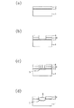
In the method for forming a twin well of a semiconductor device according to the present invention, first, a first
[0015]
Next, the
[0016]
Next, a second
[0017]
Next, the
[0018]
Next, the first insulating
[0019]
Next, using the etched back second insulating
[0020]
Next, the second insulating
[0021]
【The invention's effect】
As described above, according to the twin well forming method of a semiconductor element according to the present invention, it is possible to prevent a step from being generated on the surface of the semiconductor substrate, and the semiconductor element formed (manufactured) in the well. Reliability can be improved.
[0022]
Here, when the first insulating film is a silicon oxide film, its formation and etching are facilitated.
Further, when the second insulating film is a silicon nitride film, it functions as a mask for protecting the region into which the first impurity is implanted when selective ion implantation is performed on the semiconductor substrate.
Further, if the film thicknesses of the first buffer insulating film and the second buffer insulating film are made equal, ion implantation into the semiconductor substrate is made uniform at the depth, and the impurity diffusion distribution after the heat treatment is made uniform. .
If an SOG film is used as the planarizing material film, since the SOG is highly fluid, etching for forming the second buffer insulating film can be performed with high accuracy.
[Brief description of the drawings]
FIG. 1 is a cross-sectional view showing the first half of a semiconductor device twin well forming method according to the present invention in the order of steps;
FIG. 2 is a cross-sectional view showing the second half of a twin well forming method for a semiconductor device according to the present invention in the order of steps;
FIG. 3 is a cross-sectional view showing a first half of a conventional twin well forming method for a semiconductor device in the order of steps;
FIG. 4 is a 2/2 process longitudinal cross-sectional view showing the latter half of a conventional semiconductor device twin well forming method in the order of processes;
[Explanation of symbols]
10: Semiconductor substrate 20: First insulating film 21: First insulating film pattern 22: First buffer insulating film 23: Second buffer insulating film 30: Photosensitive resist pattern 40: Boron (first impurity)
50: Second insulating film 60: Planarizing material film 70: Phosphorus (second impurity)
Claims (6)
該第1絶縁膜に選択的なエッチングを施して該半導体基板上に第1絶縁膜パターン及び第1バッファー絶縁膜を形成する工程と、
該第1バッファー絶縁膜をその上に形成された該半導体基板の上層部に第1不純物をイオン注入する工程と、
該第1絶縁膜パターン及び第1バッファー絶縁膜の上面に第2絶縁膜を形成する工程と、
該第2絶縁膜の上面に平坦化物質膜を形成する工程と、
該第1絶縁膜パターンの上面を露出させるように該平坦化物質膜及び第2絶縁膜をエッチバックする工程と、
該第1絶縁膜パターンに選択的にエッチングを施して第2バッファー絶縁膜を形成する工程と、
該第2バッファー絶縁膜をその上に形成された該半導体基板の上層部に第2不純物をイオン注入する工程と、
該第2絶縁膜、第1バッファー絶縁膜及び第2バッファー絶縁膜を除去する工程と、
該半導体基板に熱処理を施す工程と、
を順次行うことを特徴とする半導体素子のツインウエル形成方法。Forming a first insulating film on the upper surface of the semiconductor substrate;
Performing a selective etching on the first insulating film to form a first insulating film pattern and a first buffer insulating film on the semiconductor substrate;
Ion-implanting a first impurity into an upper layer portion of the semiconductor substrate on which the first buffer insulating film is formed;
Forming a second insulating film on the top surface of the first insulating film pattern and the first buffer insulating film;
Forming a planarizing material film on the upper surface of the second insulating film;
Etching back the planarizing material film and the second insulating film so as to expose the upper surface of the first insulating film pattern;
Selectively etching the first insulating film pattern to form a second buffer insulating film;
Ion-implanting a second impurity into an upper layer of the semiconductor substrate on which the second buffer insulating film is formed;
Removing the second insulating film, the first buffer insulating film, and the second buffer insulating film;
Applying heat treatment to the semiconductor substrate;
A method for forming a twin well of a semiconductor device, wherein the steps are sequentially performed.
該第1バッファー絶縁膜をその上に形成された該半導体基板の上層部に第1不純物をイオン注入する工程と、
該第1絶縁膜及び第1バッファー絶縁膜の上面に第2絶縁膜を形成する工程と、
該第2絶縁膜の上面に平坦化物質膜を形成する工程と、
該第1絶縁膜の上面を露出させるように該平坦化物質膜及び第2絶縁膜をエッチバックする工程と、
該第1絶縁膜に選択的なエッチングを施して該第2領域の半導体基板上に第2バッファー絶縁膜を形成する工程と、
該第2バッファー絶縁膜をその上に形成された該半導体基板の上層部に第2不純物をイオン注入する工程と、
該エッチバックされた第2絶縁膜及び第1バッファー絶縁膜と該エッチングされた第2バッファー絶縁膜を除去して該半導体基板の上面を露出させる工程と、該露出させられた半導体基板に熱処理を施してその上層部にそれぞれ注入された該第1不純物及び第2不純物を該半導体基板内部で安定化させる工程と、
を順次行うことを特徴とする半導体素子のツインウエル形成方法。Forming a first insulating film on the upper surface of the first region of the semiconductor substrate having the first region and the second region, and forming a first buffer insulating film on the upper surface of the second region;
Ion-implanting a first impurity into an upper layer portion of the semiconductor substrate on which the first buffer insulating film is formed;
Forming a second insulating film on top surfaces of the first insulating film and the first buffer insulating film;
Forming a planarizing material film on the upper surface of the second insulating film;
Etching back the planarizing material film and the second insulating film so as to expose the upper surface of the first insulating film;
Performing a selective etching on the first insulating film to form a second buffer insulating film on the semiconductor substrate in the second region;
Ion-implanting a second impurity into an upper layer of the semiconductor substrate on which the second buffer insulating film is formed;
Removing the etched back second insulating film and first buffer insulating film and the etched second buffer insulating film to expose an upper surface of the semiconductor substrate; and subjecting the exposed semiconductor substrate to a heat treatment. Applying and stabilizing the first impurity and the second impurity respectively injected into the upper layer portion inside the semiconductor substrate;
A method for forming a twin well of a semiconductor device, wherein the steps are sequentially performed.
Applications Claiming Priority (2)
| Application Number | Priority Date | Filing Date | Title |
|---|---|---|---|
| KR76819/1997 | 1997-12-29 | ||
| KR1019970076819A KR100266652B1 (en) | 1997-12-29 | 1997-12-29 | Twin well formation method of semiconductor device |
Publications (2)
| Publication Number | Publication Date |
|---|---|
| JPH11274094A JPH11274094A (en) | 1999-10-08 |
| JP4171122B2 true JP4171122B2 (en) | 2008-10-22 |
Family
ID=19529349
Family Applications (1)
| Application Number | Title | Priority Date | Filing Date |
|---|---|---|---|
| JP35596798A Expired - Fee Related JP4171122B2 (en) | 1997-12-29 | 1998-12-15 | Method for forming a semiconductor device twin well |
Country Status (3)
| Country | Link |
|---|---|
| US (1) | US5985710A (en) |
| JP (1) | JP4171122B2 (en) |
| KR (1) | KR100266652B1 (en) |
Family Cites Families (3)
| Publication number | Priority date | Publication date | Assignee | Title |
|---|---|---|---|---|
| US4584027A (en) * | 1984-11-07 | 1986-04-22 | Ncr Corporation | Twin well single mask CMOS process |
| KR940009997B1 (en) * | 1991-05-03 | 1994-10-19 | 현대전자산업 주식회사 | Two-well manufacturing method without step for cmos |
| US5670395A (en) * | 1996-04-29 | 1997-09-23 | Chartered Semiconductor Manufacturing Pte. Ltd. | Process for self-aligned twin wells without N-well and P-well height difference |
-
1997
- 1997-12-29 KR KR1019970076819A patent/KR100266652B1/en not_active IP Right Cessation
-
1998
- 1998-06-16 US US09/097,389 patent/US5985710A/en not_active Expired - Lifetime
- 1998-12-15 JP JP35596798A patent/JP4171122B2/en not_active Expired - Fee Related
Also Published As
| Publication number | Publication date |
|---|---|
| JPH11274094A (en) | 1999-10-08 |
| KR100266652B1 (en) | 2000-11-01 |
| US5985710A (en) | 1999-11-16 |
| KR19990056801A (en) | 1999-07-15 |
Similar Documents
| Publication | Publication Date | Title |
|---|---|---|
| US5895252A (en) | Field oxidation by implanted oxygen (FIMOX) | |
| JP2521611B2 (en) | Method of manufacturing CMOS having twin well | |
| JPS6359251B2 (en) | ||
| JP4171122B2 (en) | Method for forming a semiconductor device twin well | |
| JPH0628282B2 (en) | Method for manufacturing semiconductor device | |
| JPH1092806A (en) | Method of forming semiconductor element isolation region | |
| JPS63110658A (en) | Manufacture of semiconductor device | |
| JP2586431B2 (en) | Method for manufacturing semiconductor device | |
| KR970007111B1 (en) | Isoating method of integrated circuit | |
| JPS6362326A (en) | Manufacture of semiconductor device | |
| JPS6261353A (en) | Manufacture of complementary mos semiconductor element | |
| JPH0779101B2 (en) | Manufacturing method of semiconductor device | |
| KR100589493B1 (en) | Method for fabricating gate oxide | |
| KR100379503B1 (en) | Method for forming oxide layer | |
| JPH01123452A (en) | Formation of trench capacitor insulating film | |
| JPS61241941A (en) | Manufacture of semiconductor device | |
| KR0124637B1 (en) | Method of forming the isolation on semiconductor device | |
| KR0166812B1 (en) | Method for forming isolation on a semiconductor device | |
| KR0167674B1 (en) | Method of forming isolation on semiconductor device | |
| JPH01173712A (en) | Manufacture of semiconductor device | |
| KR20000019635A (en) | Method for simplifying gate oxide process of semiconductor device having trench isolation | |
| JPS5919357A (en) | Manufacture of semiconductor device | |
| JPH05166746A (en) | Manufacture of semiconductor device | |
| KR19980065735A (en) | Method of forming surface step of semiconductor substrate | |
| JPH02266531A (en) | Manufacture of semiconductor device |
Legal Events
| Date | Code | Title | Description |
|---|---|---|---|
| A621 | Written request for application examination |
Free format text: JAPANESE INTERMEDIATE CODE: A621 Effective date: 20051014 |
|
| A977 | Report on retrieval |
Free format text: JAPANESE INTERMEDIATE CODE: A971007 Effective date: 20080530 |
|
| TRDD | Decision of grant or rejection written | ||
| A01 | Written decision to grant a patent or to grant a registration (utility model) |
Free format text: JAPANESE INTERMEDIATE CODE: A01 Effective date: 20080715 |
|
| A01 | Written decision to grant a patent or to grant a registration (utility model) |
Free format text: JAPANESE INTERMEDIATE CODE: A01 |
|
| A61 | First payment of annual fees (during grant procedure) |
Free format text: JAPANESE INTERMEDIATE CODE: A61 Effective date: 20080808 |
|
| FPAY | Renewal fee payment (event date is renewal date of database) |
Free format text: PAYMENT UNTIL: 20110815 Year of fee payment: 3 |
|
| R150 | Certificate of patent or registration of utility model |
Free format text: JAPANESE INTERMEDIATE CODE: R150 |
|
| FPAY | Renewal fee payment (event date is renewal date of database) |
Free format text: PAYMENT UNTIL: 20120815 Year of fee payment: 4 |
|
| FPAY | Renewal fee payment (event date is renewal date of database) |
Free format text: PAYMENT UNTIL: 20130815 Year of fee payment: 5 |
|
| LAPS | Cancellation because of no payment of annual fees |