JP4170630B2 - Termination circuit impedance update apparatus and method - Google Patents
Termination circuit impedance update apparatus and method Download PDFInfo
- Publication number
- JP4170630B2 JP4170630B2 JP2002023516A JP2002023516A JP4170630B2 JP 4170630 B2 JP4170630 B2 JP 4170630B2 JP 2002023516 A JP2002023516 A JP 2002023516A JP 2002023516 A JP2002023516 A JP 2002023516A JP 4170630 B2 JP4170630 B2 JP 4170630B2
- Authority
- JP
- Japan
- Prior art keywords
- impedance
- update
- terminator
- signal
- circuit
- Prior art date
- Legal status (The legal status is an assumption and is not a legal conclusion. Google has not performed a legal analysis and makes no representation as to the accuracy of the status listed.)
- Expired - Fee Related
Links
Images


Classifications
-
- H—ELECTRICITY
- H03—ELECTRONIC CIRCUITRY
- H03H—IMPEDANCE NETWORKS, e.g. RESONANT CIRCUITS; RESONATORS
- H03H11/00—Networks using active elements
- H03H11/02—Multiple-port networks
- H03H11/40—Impedance converters
-
- H—ELECTRICITY
- H04—ELECTRIC COMMUNICATION TECHNIQUE
- H04L—TRANSMISSION OF DIGITAL INFORMATION, e.g. TELEGRAPHIC COMMUNICATION
- H04L25/00—Baseband systems
- H04L25/02—Details ; arrangements for supplying electrical power along data transmission lines
- H04L25/0264—Arrangements for coupling to transmission lines
- H04L25/0298—Arrangement for terminating transmission lines
Landscapes
- Engineering & Computer Science (AREA)
- Power Engineering (AREA)
- Computer Networks & Wireless Communication (AREA)
- Signal Processing (AREA)
- Dc Digital Transmission (AREA)
- Logic Circuits (AREA)
- Dram (AREA)
- Memory System (AREA)
Description
【0001】
【発明の属する技術の分野】
本発明は、ターミネーション回路に関連し、特にターミネーション回路においてインピーダンスアップデートの際に発生しうるシステムノイズを最少化することができるターミネーション回路のインピーダンスアップデート装置に関する。
【0002】
【従来の技術】
最近、高速データ伝送において周波数が高くなるに従いオンチップターミネーションに対する要求が強まっている。高速データ伝送のための従来のターミネーション回路が図10に図示されている。図10に示したように、前記オンチップターミネーションは、伝送ラインを通じてデータを伝送する際に出力ドライバ1がソースターミネーションを担当し、受信側のターミネーション回路3が並列ターミネーションを担当することにより、信号のスイングレベル自体は低下するものの、信号の完結性の側面で優れたフルスイングでの伝達を可能にする。しかし、メモリを例に挙げれば、クロック、アドレス、制御信号については信号を単方向に伝送するので、前記ターミネーション回路3はチップが動作している間継続してオンされていなければならない。
【0003】
前記ターミネーション回路の構成においては、トランジスタを組み合せた並列合成インピーダンスを用いる。しかし、チップの動作環境及び内部的工程要因変化(PVT Variation: Process, Voltage, Temperature:以下、これを‘PVT’変化と称する)に起因してインピーダンスが変わるので、これをトラッキングして所定のインピーダンスを継続して維持しなければならない。このように従来の高速データ伝送のためのターミネーション回路は、チップの動作環境及び内部的PVT変化に起因するインピーダンスの変化に対応して継続的にターミネーション回路をアップデートするためのトラッキング動作により、継続動作している回路中のトランジスタの組み合せにおけるオン/オフによりシステムノイズが誘発されるという問題点がある。
【0004】
【発明が解決しようとする課題】
このように従来の高速データ伝送のためのターミネーション回路は、チップの動作環境及び内部的PVT変化に起因するインピーダンスの変化に対応して継続的にインピーダンスをアップデートするためのトラッキング動作を行うことにより、継続動作している回路中のトランジスタの組み合せにおけるオン/オフによりシステムノイズが誘発されるという問題点がある。
【0005】
本発明の目的は、ターミネーション回路のインピーダンスアップデートの際に発生しうるシステムノイズを最少化することができるターミネーション回路のインピーダンスアップデート装置を提供することにある。
【0006】
本発明の他の目的は、ターミネーション回路のインピーダンスアップデートをアップターミネーターとダウンターミネーターに分離したターミネーション回路のインピーダンスアップデート装置を提供するにある。
【0007】
【課題を解決するための手段】
このような目的を達成するため本発明によるターミネーション回路のインピーダンスアップデート装置は、アップタミネーターとダウンターミネーターとを有するターミネーター回路、及び外部入力信号のレベルを判断して前記アップまたはダウンターミネーターのインピーダンスアップデートをそれぞれ個別制御するアップデート個別制御部を具備することを特徴とする。
【0008】
そして、前記ターミネーション回路のインピーダンスアップデート装置に適用されるアップデート個別制御部は、第1例として、プログラム可能なインピーダンス制御器のインピーダンスコードをラッチしている間に、前記外部入力信号のレベルに従い継続して、該インピーダンスコードに応じたアップまたはダウンアップデートをそれぞれ行うことを特徴とする。
【0009】
また、第2例として、周期的に発生されるアップ‐アップデートイネーブル信号またはダウンアップデートイネーブル信号と前記外部の入力信号のレベルが所定条件に一致する場合にのみにアップターミネーターのインピーダンスアップデートまたはダウンターミネーターのインピーダンスアップデートを行うことを特徴とする。
【0010】
また、第3例として、セットアップ及びホールドタイムにおいてのみ、前記外部入力信号のレベルに従いアップターミネーターまたはダウンターミネーターのインピーダンスアップデートを行うことを特徴とする。
【0011】
また、外部入力信号のレベルを判断して最少電流の流れるターミネーターを検出するアップデート個別制御部とアップ/ダウン分離されたターミネーターを備えたターミネーション回路のインピーダンスアップデート方法は、外部入力信号のレベルを判断して前記アップまたはダウンターミネーターのうち最少電流の流れるターミネーター部分を検出する第1段階と、前記第1段階で検出された最少電流が流れるターミネーター部分のみのインピーダンスアップデートを制御する第2段階とを含むことを特徴とする。
【0012】
そして、前記第1段階は、セットアップタイム及びホールドタイムにおいてのみ行うか、または周期的に発生されるアップデートイネーブル信号がある場合にのみ行うことを特徴とする。
【0013】
【発明の実施の形態】
以下、本発明の好適な実施の形態のターミネーション回路を図1乃至図3を用いて説明する。
【0014】
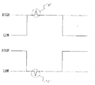
図1は、本発明の好適な実施の形態としてのターミネーションのための回路を示した図である。この回路は、アップターミネーター31とダウンターミネーター33とが分離してそれぞれ駆動されるターミネーション回路である。本発明に適用されうるターミネーションのための回路を説明するため、図1にはトランスミッター(transmitter)回路10とレシーバー(receiver)回路20とターミネーター回路30が示されている。ここで、ターミネーター回路30はアップターミネーター31とダウンターミネーター33に区分されている。ターミネーター回路30はターミネーションのための回路であり、レシーバー回路20は入力バッファである。ターミネーター回路30は、特定コードで全てのトランジスタがオンまたはオフにトランジションしうる。この場合、回路を如何にデザインしても、図2aに示すように、トランジスタが全てオン(論理符号‘11111’)されるグリッチ(glitch)状態と、図2bに示すようにトランジスタの全てがオフ(論理符号‘00000’)されるグリッチ状態が存在する。
【0015】
図2aは、ターミネーター回路が全てオントランジション(on transition)状態となるタイミングを含む動作図である。論理符号‘11111’の‘a’または‘b’区間において、‘ア’または‘イ’のようにトランジスタが全てオンされる状態では前記ターミネーター回路がオープンされたように見えるので、伝送される‘ハイ’信号が瞬間的に上方に飛ぶ現象(‘ロー’信号は下方に飛ぶ。即ち、信号の正常なスイング範囲の外側に信号が飛ぶ現象)が発生する。この信号は再びトランスミッター10回路に反射されて信号の歪曲を誘発させる。
【0016】
図2bは、ターミネーター回路が全てオフトランジション(off transition)状態となるタイミングを含む動作図である。論理符号‘00000’の‘c’または‘d’区間において、‘ウ’または‘エ’のようにトランジスタが全てオフされる状態では前記ターミネーター回路が瞬間的に相当に低いインピーダンスとなるので、伝送される‘ハイ’信号が瞬間的に下方に飛ぶ現象(‘ロー’信号は上方に飛ぶ。即ち、信号の正常なスイングレベルの内側に信号が飛ぶ現象)が発生する。この信号もやはり再びトランスミッター回路10に反射されて信号の歪曲を誘発させる。
【0017】
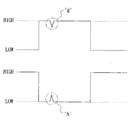
図3aは図2aのようにターミネーター回路が全てオントランジション状態となったときのグリッチ信号波形を示した図であり、図3bは図2bのようにターミネーター回路が全てオフトランジション状態になったときのグリッチ信号波形を示した図である。
【0018】
以上説明したように、図1によるターミネーション回路でインピーダンスのアップデートの際に発生する信号歪曲を最少化するインピーダンスアップデート装置を以下に説明する。
【0019】
ターミネーション回路のインピーダンスアップデートの際のシステムノイズの発生は、インピーダンスアップデートを図1に示した本発明の好適な実施の形態のターミネーション回路のようにアップターミネーターとダウンターミネーターに分離することにより、ある程度解決することができる。なお、この場合においてもアップ/ダウン信号に従いノイズが発生しうる。しかし、このような問題も、ターミネーション回路のインピーダンスがトランスミッター回路のインピーダンスよりも大きいことを利用し、外部入力信号のレベルに従ってアップ/ダウンターミネーター回路のインピーダンスアップデートを別々に行うことにより最少化することができる。
【0020】
以下、本発明のより改善された好ましい実施の形態を図面を用いて詳しく説明する。なお、関連する図面において、同一の構成要素には同一の符号を付した。
図4a、図4bは、本発明の好適な実施の形態において、アップターミネーター回路とダウンターミネーター回路とでインピーダンスアップデートを分離して行うための概念図である。より詳しくは、図4aはアップターミネーター回路のインピーダンスアップデートの概念を示した回路構成図であり、図4bはダウンターミネーター回路のインピーダンスアップデートの概念を示した回路構成図である。
【0021】
図4aに示すように、トランスミッター回路10が‘ハイ’信号を送るとき、トランスミッター回路10とターミネーター回路30に流れる電流を見ると、ターミネーター回路30のダウンドライバ側(抵抗NR2)に流れる電流I3が最も大きく、トランスミッター回路10の抵抗R1に流れる電流I1が二番目に大きく、ターミネーター回路30のアップドライブ側(抵抗NR1)に流れる電流I2が最も小さい。このとき、最少電流が流れる前記アップドライブ側のターミネーションインピーダンスをアップデートさせると、信号の歪曲を最少化することができる。ここで、記号‘N’は1よりも大きい実数を意味する。
【0022】
反対に、図4bに示すように、トランスミッター回路10が‘ロー’信号を送るとき、トランスミッター回路10とターミネーター回路30に流れる電流を見ると、ターミネーター回路30のアップドライブ側(抵抗NR11)に流れる電流I21が最も大きく、前記トランスミッター回路10の抵抗R11に流れる電流I11が二番目に大きく、前記ターミネーター回路30のダウンドライブ側(抵抗NR21)に流れる電流I31が最も小さい。このときにも最少電流が流れる前記ダウンドライブ側のターミネーションインピーダンスをアップデートさせると、信号の歪曲を最少化することができる。ここで、記号‘N’は1よりも大きい実数を意味する。
【0023】
即ち、本発明の好適な実施の形態では、アップドライブ側とダウンドライブ側のそれぞれに対するインピーダンスアップデートを実行する。そして、この際に、外部信号を用いてアップドライブまたはダウンドライブのうち最少電流が流れるドライブを検出した後、その検出結果に従って、最少電流が流れるドライブ側のインピーダンスを制御して信号の歪曲を最少化する。言い換えれば、本発明の好適な実施の形態では、アップドライブ及びダウンドライブのインピーダンスアップデートを個別的に実行する。そして、その際に、入力信号のレベルに従って最少電流の流れるドライブ側を判断して、最少電流が流れるドライブ側のインピーダンスアップデートを実行することにより、信号の歪曲を最少化する。
【0024】
本発明に係るターミネーション回路のインピーダンスアップデート装置は、アップまたはダウンアップデートの個別制御を以下の三つの方法のいずれかにより実現することが好ましい。
【0025】
第1の方法は、プログラム可能なインピーダンス制御器(PIC; Programmable Impedance Controller)で生成されたインピーダンスコードをホールドしながら、セットアップタイムにおいて前記外部入力信号のレベルに従い継続してアップまたはダウンアップデート制御信号を発生する方法である。
【0026】
第2の方法は、ホールドタイム毎に外部入力信号のレベルに従い継続してアップまたはダウンアップデート制御信号を発生する方法である。
【0027】
第3の方法は、周期的に発生されるアップ−アップデートイネーブル信号またはダウン‐アップデートイネーブル信号と外部の入力信号のレベルが所定条件に一致する場合のみにアップ‐アップデートまたはダウン‐アップデートを制御する制御信号を発生する方法である。
【0028】
まず、第1の方法、すなわちセットアップタイムにおいてアップデートする方法を適用した装置を本発明の第1実施例として図5及び図6を参照して説明する。図5は本発明の第1実施例の入力信号レベルによるターミネーション回路のインピーダンスアップデート装置の回路構成図であり、図6は図5に示す回路に備えられたインバーターの特性を示した図である。
【0029】
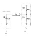
図4に示した入力信号レベルによるターミネーション回路のインピーダンスアップデート装置の回路構成は以下の通りである。図中のパッドは図1に示したトランスミッター回路10の出力上に存在するものであり、前記パッドの出力にアップ‐ターミネーター31、ダウン‐ターミネーター33及びレシーバー20が連結されている。アップ‐ターミネーター31は静電圧源のVDDQと連結されている。アップ‐ターミネーター31は、プログラム可能なインピーダンスのアップ制御器(PIUC; Programmable Impedance Up Controller)からのインピーダンス情報を保持するラッチ41に連結されている。そして、ダウン‐ターミネーター33も、プログラム可能なインピーダンスのダウン制御器(PIDC; Programmable Impedance Down Controller)からのインピーダンス情報を保持するラッチ43に連結されている。
【0030】
前記パッドは、アップ‐ターミネーター31と連結されたラッチ41に連結されているインバーターIAとダウン‐ターミネーター33と連結されたラッチ43に連結されているインバーターIBとも連結されている。
【0031】
レシーバー20は比較器で構成され、基準電圧Vrefを用いる。
【0032】
インバーターIAとラッチ41はアップ‐アップデート制御部50を構成し、インバーターIBとラッチ43はダウン‐アップデート制御部60を構成する。アップ‐アップデート制御部50とダウン‐アップデート制御部60をアップデート個別制御部と総称することにする。
【0033】
以下、図5に示した本発明の第1実施例としての入力信号レベルによるターミネーション回路のインピーダンスアップデート装置の動作を説明する。一定サイクルでアップデートされるインピーダンス情報をプログラム可能なインピーダンス制御器PIUCまたはPIDCから受けて、前記パッド側の外部入力信号レベルに従って、それぞれラッチ41またはラッチ43で保持しながら、アップ側のラッチ41とダウン側のラッチ43によりアップ‐ターミネーター31またはダウン‐ターミネーター33のインピーダンスがアップデートされる。
【0034】
ここで、前記パッドに連結されたインバーターIA、IBの特性は図6に示す通りである。即ち、外部入力信号が充分に‘ハイ’となるとき、インバーターIAが遷移して、最少電流が流れるアップ‐ターミネーター31に対してアップデートされたインピーダンス情報を渡す。反対に、外部入力信号が充分に‘ロー’となるとき、インバーターIBが遷移して最少電流が流れるダウン‐ターミネーター33に対してアップデートされたインピーダンス情報を渡す。
【0035】
よって、外部入力信号のレベルに従ってインピーダンスのアップまたはダウンアップデートを個別的に継続して制御することができる。言い換えれば、アップデート個別制御部50,60は、外部入力信号のレベルを判断し、それに従って最少電流が流れるターミネーターへのアップまたはダウンインピーダンスアップデートをそれぞれ制御する制御信号(インピーダンス情報)を発生し、アップ‐ターミネーター31またはダウン‐ターミネーター33に伝達する。
【0036】
アップ‐ターミネーター31は、アップ‐アップデート制御部50からアップインピーダンスアップデートを制御する制御信号としてのインピーダンス情報が印加されると、そのインピーダンス情報に従ってインピーダンスをアップデートする。ダウン‐ターミネーター33は、ダウンアップデート制御部60からダウンインピーダンスアップデートを制御する制御信号としてのインピーダンス情報が印加されると、そのインピーダンス情報に従ってインピーダンスをアップデートする。
【0037】
次に、第2の方法、すなわちホールドタイム毎に外部入力信号のレベルに従って最少電流が流れるターミネーター回路のアップまたはダウンアップデート制御信号を継続して発生する方法を適用した装置を本発明の第2実施例として図7を参照して説明する。図7は、本発明の第2実施例としての入力信号レベルによるターミネーション回路のインピーダンスアップデート装置の回路構成図である。図7に示した入力信号レベルによるターミネーション回路のインピーダンスアップデート装置の回路構成は以下の通りである。
【0038】
図中のパッドは図1に示したトランスミッター回路10の出力上に存在するパッドであり、前記パッドの出力にアップ‐ターミネーター31、ダウン‐ターミネーター33及びレシーバー20が連結されている。アップ‐ターミネーター31は、プログラム可能なインピーダンスのアップ制御器PIUCからのインピーダンス情報を保持するラッチ61に連結され、ダウン‐ターミネーター33はプログラム可能なインピーダンスのダウン制御器PIDCからのインピーダンス情報を保持するラッチ63に連結されている。
【0039】
レシーバー20は比較器で構成され、基準電圧Vrefを用いる。レシーバー20の出力は入力バッファ70に連結されている。入力バッファ70の出力はラッチ61に連結され、入力バッファ70の出力の反転信号はラッチ63に連結される。入力バッファ70は比較器で構成され、内部クロック信号Klatchによって制御される。ここで、ラッチ61,63及び入力バッファ70はアップデート個別制御部80を構成する。
【0040】
図7に示した本発明の第2実施例の入力信号レベルによるターミネーション回路のインピーダンスアップデート装置の動作を説明すると、一定サイクルでアップデートされたインピーダンス情報をプログラム可能なインピーダンス制御器PIUCまたはPIDCで受けて、それぞれラッチ61またはラッチ63で保持する。
【0041】
前記パッドを通して入力される外部入力信号は、レシーバー20を経て入力バッファ70に入力される。入力バッファ70がその入力信号を内部クロック信号Klatchに従ってCMOSレベルでホールドしている間に、入力信号レベル(アップまたはダウン)に従って、すなわち、(入力信号レベルに従って)最少電流が流れるターミネーターがアップ側であるかダウン側であるかに応じて、PIUCまたはPIDCで受けてラッチ61または63に保持されたインピーダンス情報をアップ‐ターミネーター31またはダウン‐ターミネーター33に対してインピーダンス情報を伝達することによりインピーダンスのアップデートを実現する。
【0042】
よって、内部クロック信号によって定められうるホールドタイム毎に外部入力信号のレベルに従って継続してアップまたはダウンアップデート制御信号を発生させて、インピーダンスのアップまたはダウンアップデートを個別的に制御し、これにより信号歪曲を防止することができる。
【0043】
言い換えれば、アップデート個別制御部80は外部入力信号のレベルを判断して最小電流の流れるターミネーター回路のアップまたはダウンインピーダンスアップデートをそれぞれ制御する制御信号を発生してアップ‐ターミネーター31またはダウン‐ターミネーター33に伝達する。アップ‐ターミネーター31は、アップデート個別制御部80から前記アップインピーダンスアップデートを制御する制御信号としてのインピーダンス情報が印加されると、そのインピーダンス情報に従ってインピーダンスをアップデートする。ダウン‐ターミネーター33は、アップデート個別制御部80から前記ダウンインピーダンスアップデートを制御する制御信号としてのインピーダンス情報が印加されると、そのインピーダンス情報に従ってインピーダンスをアップデートする。
【0044】
最後に、第3の方法、すなわち周期的に発生されるアップ‐アップデートイネーブル信号またはダウン‐アップデートイネーブル信号と外部の入力信号のレベルが所定条件に一致する場合にのみアップ‐アップデートまたはダウン‐アップデートを制御する制御信号を発生する方法を適用した装置を図8及び図9を参照して本発明の第3実施例及び第4実施例として説明する。
【0045】
まず、図8は、本発明の第3実施例としての外部信号によるターミネーション回路のインピーダンスアップデート装置、より詳しくは、セットアップタイムごとに周期的に発生されるイネーブル信号と外部入力信号によるターミネーション回路のインピーダンスアップデート装置の回路構成図である。図8に示したターミネーション回路のインピーダンスアップデート装置の回路構成は以下の通りである。
【0046】
図中のパッドは図1に示したトランスミッター回路10の出力上に存在するパッドであり、前記パッドの出力にアップ‐ターミネーター31、ダウン‐ターミネーター33及びレシーバー20が連結されている。アップ‐ターミネーター31は静電圧源VDDQと連結されている。アップ‐ターミネーター31はプログラム可能なインピーダンスのアップ制御器PIUCからのインピーダンス情報を保持するラッチ91に連結され、ダウン‐ターミネーター33はプログラム可能なインピーダンスのダウン制御器PIDCからのインピーダンス情報を保持するラッチ93に連結されている。
【0047】
前記パッドは、インバーターIAとインバーターIBとにそれぞれ連結され、インバーターIAはNANDゲートNAND1の入力に連結され、インバーターIBはNANDゲートNAND2の入力に連結されている。NANDゲートNAND1の他の入力にはアップ‐アップデートイネーブル信号が連結され、出力がラッチ91に連結されている。そして、NANDゲートNAND2の他の入力にはダウン‐アップデートイネーブル信号が連結され、出力がラッチ93に連結されている。
【0048】
レシーバー20は比較器で構成され、基準電圧Vrefを用いる。
【0049】
インバーターIA、NAND1及びラッチ91は、アップ‐アップデート制御部90を構成し、インバーターIB、NAND2及びラッチ93は、ダウン‐アップデート制御部100を構成する。アップ‐アップデート制御部90とダウン‐アップデート制御部100をアップデート個別制御部と総称することにする。
【0050】
図8に示した本発明の第3実施例の外部入力信号とアップ‐アップデートイネーブル信号とダウン‐アップデートイネーブル信号によるターミネーション回路のインピーダンスアップデート装置は、図5に示したターミネーション回路のインピーダンスアップデート装置が外部入力信号に従い継続してアップデートされなければならないという点を補完した装置である。
【0051】
すなわち、この装置は、チップ内で一定した間隔のアップ‐アップデートイネーブル信号とダウン‐アップデートイネーブル信号を発生させて、この信号がアクティブレベルで外部信号が所定レベルであるときのみにアップデートを実行することにより、継続してアップデートを実行する。これにより、システムに与える負荷を減少させることができる。
【0052】
さらに言い換えれば、アップデート個別制御部90,100は外部入力信号のレベルを判断してアップまたはダウンインピーダンスアップデートをそれぞれ制御する制御信号を発生してアップ‐ターミネーター31またはダウン‐ターミネーター33に伝達する。アップ‐ターミネーター31は、アップ‐アップデート制御部90からアップインピーダンスアップデートを制御する制御信号としてのインピーダンス情報が印加されると、そのインピーダンス情報に従ってインピーダンスをアップデートする。ダウン‐ターミネーター33は、ダウンアップデート制御部100からダウンインピーダンスアップデートを制御する制御信号としてのインピーダンス情報が印加されると、そのインピーダンス情報に従ってインピーダンスをアップデートする。
【0053】
最後に、図9は、本発明の第4実施例の外部信号によるターミネーション回路のインピーダンスアップデート装置、より詳しくは、ホールドタイムごとに周期的に発生されるイネーブル信号と外部入力信号によるターミネーション回路のインピーダンスアップデート装置の回路構成図である。この装置の回路構成は以下の通りである。
【0054】
パッドは図1に示したトランスミッター回路10の出力上に存在するパッドであり、前記パッドの出力にアップ‐ターミネーター31、ダウン‐ターミネーター33及びレシーバー20が連結されている。アップ‐ターミネーター31はプログラム可能なインピーダンスのアップ制御器PIUCからのインピーダンス情報を保持するラッチ111に連結され、ダウン‐ターミネーター33はプログラム可能なインピーダンスのダウン制御器PIDCからのインピーダンス情報を保持するラッチ113に連結されている。
【0055】
レシーバー20は比較器で構成され、基準電圧Vrefを用いる。レシーバー20の出力は入力バッファ120に連結され、入力バッファ120の出力はNANDゲートNAND11の入力及びANDゲートAND21の入力に連結されている。NANDゲートNAND11の他の入力にはアップ‐アップデートイネーブル信号が連結され、出力がラッチ111に連結されている。そして、ANDゲートAND21の他の入力にはダウン‐アップデートイネーブル信号が連結され、出力がラッチ113に連結されている。入力バッファ120は比較器で構成され、クロック入力端子が内部クロック信号Klatchに連結されている。ここで、ラッチ111、ラッチ113、NAND11、AND21及び入力バッファ120は、アップデート個別制御部130を構成する。
【0056】
図9に示した本発明の第4実施例の外部信号によるターミネーション回路のインピーダンスアップデート装置の動作も図8に示したターミネーション回路のインピーダンスアップデート装置と類似した動作をする。具体的には、チップ内で一定した間隔のアップ‐アップデートイネーブル信号とダウン‐アップデートイネーブル信号を発生させて、この信号がアクティブレベルで外部信号が所定レベルであるときにのみインピーダンスアップデートをアップ/ダウン個別的に制御し、システムに与える負荷を減少させる。
【0057】
言い換えれば、アップデート個別制御部130は外部入力信号のレベルを判断してアップまたはダウンインピーダンスアップデートをそれぞれ制御する制御信号を発生してアップ‐ターミネーター31またはダウン‐ターミネーター33に伝達する。アップ‐ターミネーター31は、アップデート個別制御部130から前記アップ‐インピダンスアップデートを制御する制御信号としてのインピーダンス情報が印加されると、そのインピーダンス情報に従ってインピーダンスをアップデートする。ダウン‐ターミネーター33は、アップデート個別制御部130から前記ダウンインピダンスアップデートを制御する制御信号としてのインピーダンス情報が印加されると、そのインピーダンス情報に従ってインピーダンスをアップデートする。
【0058】
このような本発明の好ましい実施例は、ターミネーター回路20をアップターミネーター31とダウンターミネーター33に区分し、トランスミッター回路10から入力される外部入力信号のレベルに従い前記アップまたはダウンターミネーターのうち電流が一番少なく流れるターミネーター側のインピーダンスをアップデートするアップデート方法を適用したものである。
【0059】
従って、本発明の好ましい実施例では、ターミネーション回路のインピーダンスアップデートの制御において、アップまたはダウンターミネーターのうち外部入力信号を用いて最少電流の流れるターミネーターを検出し、最少電流が流れるターミネーターのインピーダンスアップデートを行うことにより、アップ/ダウンターミネーターのインピーダンスアップデートを個別的に制御する。
【0060】
本発明は、上記の実施例以外の装置によっても実施することができる。例えば、アップ/ダウンターミネーターにそれぞれ電流比較器を連結して、両ターミネーターのうち小さい電流が流れるターミネーターを感知して、これに従ってアップまたはダウンターミネーターのそれぞれに対してインピーダンスアップデートを実行することもできる。なお、ここではその具体的な回路は省略する。
【0061】
一方、本発明の詳細な説明では具体的な実施例を例示的に挙げて説明したが、本発明の技術的思想を逸脱しない範囲で様々な変形が可能であることは勿論である。従って、本発明の技術的範囲は、上記の実施例によって限定解釈されるべきものではなく、特許請求の範囲に基づいて解釈されるべきであり、また、特許請求の範囲に記載された発明と均等な範囲にも保護範囲が及ぶものと解釈されるべきである。
【0062】
【発明の効果】
以上説明したように本発明によれば、例えば、ターミネーション回路のインピーダンスアップデートをアップまたはダウン別に個別的に制御することによりシステムノイズの発生を減少させることができるという効果がある。
【0063】
また、本発明によれば、例えば、ターミネーション回路のインピーダンスアップデートをアップ及びダウンに分離して制御し、セットアップタイム及びホールドタイムのように、特定時間にのみ又は周期的にのみインピーダンスアップデートを行うことにより、システムノイズの発生を最少にしながらシステム負荷を減少させることができるという効果がある。
【図面の簡単な説明】
【図1】本発明の好適な実施の形態のターミネーションのための回路を示した図である。
【図2a】ターミネーター回路が全てオントランジション状態の動作図である。
【図2b】ターミネーター回路が全てオフトランジション状態の動作図である。
【図3a】図2aのようにターミネーター回路が全てオントランジション状態におけるグリッチ信号波形を示した図である。
【図3b】図2bのようにターミネーター回路が全てオフトランジション状態におけるグリッチ信号波形を示した図である。
【図4a】アップ/ダウンターミネーター回路のインピーダンスアップデートを分離して行う発明を適用したアップ‐ターミネーター回路のインピーダンスアップデート概念を示した回路構成図である。
【図4b】アップ/ダウンターミネーター回路のインピーダンスアップデートを分離して行う発明を適用したダウン‐ターミネーター回路のインピーダンスアップデート概念を示した回路構成図である。
【図5】本発明の第1実施例としての入力信号レベルによるターミネーション回路のインピーダンスアップデート装置の回路構成図である。
【図6】図5に具備されるインバーター特性を示した図である。
【図7】本発明の第2実施例としての入力信号レベルによるターミネーション回路のインピーダンスアップデート装置の回路構成図である。
【図8】本発明の第3実施例としての外部信号によるターミネーション回路のインピーダンスアップデート装置の回路構成図である。
【図9】本発明の第4実施例としての外部信号によるターミネーション回路のインピーダンスアップデート装置の回路構成図である。
【符号の説明】
10:トランスミッター回路
20:レシーバー回路
30:ターミネーター回路
31:アップ‐ターミネーター
33:ダウン‐ターミネーター
50,90:アップ‐アップデート制御部
60,100:ダウン‐アップデート制御部
70,120:入力バッファ
80,130:アップデート個別制御部[0001]
[Field of the Invention]
The present invention relates to a termination circuit, and more particularly to an impedance update device for a termination circuit that can minimize system noise that may occur during impedance update in the termination circuit.
[0002]
[Prior art]
Recently, the demand for on-chip termination has increased as the frequency has increased in high-speed data transmission. A conventional termination circuit for high speed data transmission is shown in FIG. As shown in FIG. 10, in the on-chip termination, when the data is transmitted through the transmission line, the output driver 1 is in charge of source termination, and the reception-side termination circuit 3 is in charge of parallel termination. Although the swing level itself is lowered, transmission with a full swing that is excellent in terms of signal completeness is enabled. However, taking a memory as an example, the clock, address, and control signals are transmitted in a single direction, so the termination circuit 3 must be continuously turned on while the chip is operating.
[0003]
In the configuration of the termination circuit, a parallel combined impedance in which transistors are combined is used. However, the impedance changes due to the operating environment of the chip and changes in internal process factors (PVT Variation: Process, Voltage, Temperature: hereinafter referred to as 'PVT' change). Must be maintained continuously. As described above, the conventional termination circuit for high-speed data transmission is continuously operated by the tracking operation for continuously updating the termination circuit in response to the change in impedance due to the operating environment of the chip and the internal PVT change. There is a problem that system noise is induced by ON / OFF in a combination of transistors in a circuit.
[0004]
[Problems to be solved by the invention]
As described above, the conventional termination circuit for high-speed data transmission performs a tracking operation to continuously update the impedance in response to a change in impedance due to the operating environment of the chip and an internal PVT change. There is a problem that system noise is induced by ON / OFF in a combination of transistors in a continuously operating circuit.
[0005]
An object of the present invention is to provide an impedance update device for a termination circuit that can minimize system noise that may occur during impedance update of the termination circuit.
[0006]
Another object of the present invention is to provide an impedance update device for a termination circuit in which the impedance update of the termination circuit is separated into an up terminator and a down terminator.
[0007]
[Means for Solving the Problems]
In order to achieve such an object, an impedance update apparatus for a termination circuit according to the present invention includes a terminator circuit having an up terminator and a down terminator, and determines the level of an external input signal to update the impedance of the up or down terminator. An update individual control unit that performs individual control is provided.
[0008]
The update individual control unit applied to the impedance update device of the termination circuit continues according to the level of the external input signal while latching the impedance code of the programmable impedance controller as a first example. Thus, the up or down update is performed according to the impedance code.
[0009]
In addition, as a second example, only when the up-update enable signal or down-update enable signal generated periodically and the level of the external input signal match a predetermined condition, the impedance update or down-terminator of the up-terminator is changed. Impedance update is performed.
[0010]
Further, as a third example, the impedance update of the up terminator or the down terminator is performed only in the setup and hold times according to the level of the external input signal.
[0011]
In addition, the impedance update method of the termination circuit with the update individual control unit that detects the level of the external input signal to detect the terminator through which the minimum current flows and the terminator separated up / down determines the level of the external input signal. A first step of detecting a terminator portion through which the minimum current flows among the up or down terminators, and a second step of controlling impedance update of only the terminator portion through which the minimum current detected in the first step flows. It is characterized by.
[0012]
The first step is performed only during the setup time and the hold time, or only when there is an update enable signal generated periodically.
[0013]
DETAILED DESCRIPTION OF THE INVENTION
A termination circuit according to a preferred embodiment of the present invention will be described below with reference to FIGS.
[0014]
FIG. 1 is a diagram showing a circuit for termination as a preferred embodiment of the present invention. This circuit is a termination circuit in which the up
[0015]
FIG. 2a is an operation diagram including the timing when all the terminator circuits are in an on transition state. In the section “a” or “b” of the logical code “11111”, the terminator circuit appears to be opened when all the transistors are turned on as “a” or “b”. A phenomenon occurs in which a “high” signal instantaneously flies upward (a “low” signal flies downward, ie, a signal flies outside the normal swing range of the signal). This signal is reflected back to the
[0016]
FIG. 2b is an operation diagram including the timing when all the terminator circuits are in the off transition state. Since the terminator circuit instantaneously has a considerably low impedance in the state where the transistors are all turned off like 'c' or 'd' in the section 'c' or 'd' of the logical code '00000', transmission The phenomenon that the “high” signal that is generated instantaneously flies downward (the “low” signal flies upward, that is, the signal flies inside the normal swing level of the signal) occurs. This signal is also reflected back to the
[0017]
Fig. 3a shows the glitch signal waveform when all the terminator circuits are in the on-transition state as shown in Fig. 2a. It is the figure which showed the glitch signal waveform.
[0018]
As described above, an impedance update apparatus for minimizing signal distortion that occurs when impedance is updated in the termination circuit of FIG. 1 will be described below.
[0019]
Generation of system noise during the impedance update of the termination circuit can be solved to some extent by separating the impedance update into an up-terminator and a down-terminator as in the termination circuit of the preferred embodiment of the present invention shown in FIG. be able to. Even in this case, noise may be generated according to the up / down signal. However, this problem can be minimized by using the impedance of the termination circuit larger than the impedance of the transmitter circuit and separately performing the impedance update of the up / down terminator circuit according to the level of the external input signal. it can.
[0020]
Hereinafter, preferred and improved embodiments of the present invention will be described in detail with reference to the drawings. In the related drawings, the same components are denoted by the same reference numerals.
FIGS. 4a and 4b are conceptual diagrams for performing impedance update separately in an up-terminator circuit and a down-terminator circuit in a preferred embodiment of the present invention. More specifically, FIG. 4a is a circuit configuration diagram showing the concept of impedance update of the upterminator circuit, and FIG. 4b is a circuit configuration diagram showing the concept of impedance update of the downterminator circuit.
[0021]
As shown in FIG. 4a, when the
[0022]
Conversely, as shown in FIG. 4b, when the
[0023]
In other words, in the preferred embodiment of the present invention, impedance update is performed for each of the updrive side and the downdrive side. At this time, an external signal is used to detect the drive through which the minimum current flows among up-drive and down-drive, and the impedance on the drive side through which the minimum current flows is controlled according to the detection result to minimize the signal distortion. Turn into. In other words, in the preferred embodiment of the present invention, the up-drive and down-drive impedance updates are performed individually. At that time, the drive side through which the minimum current flows is determined according to the level of the input signal, and the impedance of the drive side through which the minimum current flows is executed, thereby minimizing the signal distortion.
[0024]
The termination circuit impedance update apparatus according to the present invention preferably implements individual control of up- or down-update by any of the following three methods.
[0025]
The first method is to hold an impedance code generated by a programmable impedance controller (PIC) and continuously up or down an update control signal according to the level of the external input signal at a setup time. It is a method that occurs.
[0026]
The second method is a method of generating an up or down update control signal continuously according to the level of the external input signal every hold time.
[0027]
The third method is a control for controlling up-update or down-update only when the levels of the periodically generated up-update enable signal or down-update enable signal and the external input signal match a predetermined condition. A method for generating a signal.
[0028]
First, an apparatus to which the first method, that is, the method of updating at the setup time is applied will be described as a first embodiment of the present invention with reference to FIGS. FIG. 5 is a circuit configuration diagram of the impedance update device of the termination circuit according to the input signal level of the first embodiment of the present invention, and FIG. 6 is a diagram showing the characteristics of the inverter provided in the circuit shown in FIG.
[0029]
The circuit configuration of the impedance update device of the termination circuit according to the input signal level shown in FIG. 4 is as follows. The pads in the figure are present on the output of the
[0030]
The pad is also connected to an inverter IA connected to a
[0031]
The
[0032]
The inverter IA and the
[0033]
The operation of the impedance update device of the termination circuit according to the input signal level as the first embodiment of the present invention shown in FIG. 5 will be described below. Receives impedance information that is updated in a certain cycle from the programmable impedance controller PIUC or PIDC, According to the external input signal level on the pad side, While holding with
[0034]
Here, the characteristics of the inverters IA and IB connected to the pads are as shown in FIG. That is, when the external input signal is sufficiently high, the inverter IA transitions and passes the updated impedance information to the up-
[0035]
Therefore, the impedance up or down update can be individually and continuously controlled according to the level of the external input signal. In other words, the update
[0036]
When the impedance information as a control signal for controlling the up-impedance update is applied from the up-
[0037]
Next, a second embodiment of the present invention is applied to an apparatus to which the second method, that is, a method of continuously generating an up or down update control signal for a terminator circuit in which a minimum current flows according to the level of an external input signal every hold time. An example will be described with reference to FIG. FIG. 7 is a circuit configuration diagram of an impedance update device for a termination circuit according to an input signal level as a second embodiment of the present invention. The circuit configuration of the impedance update device for the termination circuit according to the input signal level shown in FIG. 7 is as follows.
[0038]
The pads in the figure are the pads existing on the output of the
[0039]
The
[0040]
The operation of the impedance update device of the termination circuit according to the input signal level of the second embodiment of the present invention shown in FIG. 7 will be described. The impedance information updated in a certain cycle is received by the programmable impedance controller PIUC or PIDC. These are held by
[0041]
An external input signal input through the pad is input to the
[0042]
Therefore, the up or down update control signal is continuously generated according to the level of the external input signal for each hold time that can be determined by the internal clock signal, and the impedance up or down update is individually controlled, thereby signal distortion. Can be prevented.
[0043]
In other words, the update
[0044]
Finally, the third method, that is, the up-update or down-update is performed only when the periodically generated up-update enable signal or down-update enable signal and the level of the external input signal match predetermined conditions. An apparatus to which a method for generating a control signal to be controlled is applied will be described as a third embodiment and a fourth embodiment of the present invention with reference to FIGS.
[0045]
First, FIG. 8 shows an impedance update device for a termination circuit using an external signal according to a third embodiment of the present invention. More specifically, FIG. It is a circuit block diagram of an update apparatus. The circuit configuration of the impedance update device of the termination circuit shown in FIG. 8 is as follows.
[0046]
The pads in the figure are the pads existing on the output of the
[0047]
The pads are connected to an inverter IA and an inverter IB, respectively. The inverter IA is connected to an input of a NAND gate NAND1, and the inverter IB is connected to an input of a NAND gate NAND2. An up-update enable signal is connected to the other input of the NAND gate NAND1, and an output is connected to the
[0048]
The
[0049]
The inverter IA, NAND1, and the
[0050]
The impedance update device of the termination circuit using the external input signal, the up-update enable signal, and the down-update enable signal of the third embodiment of the present invention shown in FIG. 8 is the same as the impedance update device of the termination circuit shown in FIG. This device complements the point that it must be continuously updated according to the input signal.
[0051]
That is, this device generates an up-update enable signal and a down-update enable signal at regular intervals in the chip, and performs an update only when this signal is active and the external signal is at a predetermined level. Continue to update. Thereby, the load given to the system can be reduced.
[0052]
In other words, the update
[0053]
Finally, FIG. 9 shows an impedance update device for a termination circuit using an external signal according to a fourth embodiment of the present invention. More specifically, FIG. 9 shows the impedance of the termination circuit using an enable signal periodically generated every hold time and an external input signal. It is a circuit block diagram of an update apparatus. The circuit configuration of this device is as follows.
[0054]
The pad is a pad existing on the output of the
[0055]
The
[0056]
The operation of the impedance update device of the termination circuit according to the external signal of the fourth embodiment of the present invention shown in FIG. 9 is similar to the operation of the impedance update device of the termination circuit shown in FIG. Specifically, an up-update enable signal and a down-update enable signal are generated at regular intervals in the chip, and impedance update is up / down only when this signal is active and the external signal is at a predetermined level. Control individually and reduce the load on the system.
[0057]
In other words, the update
[0058]
In the preferred embodiment of the present invention, the
[0059]
Accordingly, in the preferred embodiment of the present invention, in the impedance update control of the termination circuit, the terminator through which the minimum current flows is detected using the external input signal among the up and down terminators, and the impedance update of the terminator through which the minimum current flows is performed. By controlling the impedance update of the up / down terminator individually.
[0060]
The present invention can be implemented by apparatuses other than the above-described embodiments. For example, a current comparator may be connected to each of the up / down terminators to detect a terminator through which a small current flows between the two terminators, and perform an impedance update for each of the up or down terminators accordingly. Note that a specific circuit thereof is omitted here.
[0061]
On the other hand, in the detailed description of the present invention, specific examples have been described as examples. However, it goes without saying that various modifications can be made without departing from the technical idea of the present invention. Therefore, the technical scope of the present invention should not be construed as limited by the above-described embodiments, but should be construed based on the scope of the claims, and the invention described in the scope of the claims It should be construed that the scope of protection extends to an equivalent scope.
[0062]
【The invention's effect】
As described above, according to the present invention, for example, the occurrence of system noise can be reduced by individually controlling the impedance update of the termination circuit for each up or down.
[0063]
Further, according to the present invention, for example, the impedance update of the termination circuit is controlled separately up and down, and the impedance update is performed only at a specific time or periodically, such as a setup time and a hold time. The system load can be reduced while minimizing the occurrence of system noise.
[Brief description of the drawings]
FIG. 1 is a diagram illustrating a termination circuit according to a preferred embodiment of the present invention.
FIG. 2a is an operation diagram in which all terminator circuits are in an on transition state.
FIG. 2b is an operation diagram in which all terminator circuits are in an off-transition state.
FIG. 3a is a diagram showing a glitch signal waveform when all terminator circuits are in an on-transition state as shown in FIG. 2a.
FIG. 3b is a diagram showing a glitch signal waveform when all the terminator circuits are in an off-transition state as shown in FIG. 2b.
FIG. 4A is a circuit configuration diagram showing an impedance update concept of an up-terminator circuit to which an invention in which impedance update of the up / down terminator circuit is separately performed is applied.
FIG. 4B is a circuit configuration diagram illustrating an impedance update concept of a down-terminator circuit to which an invention in which impedance update of the up / down terminator circuit is separately performed is applied.
FIG. 5 is a circuit configuration diagram of an impedance update device for a termination circuit according to an input signal level as a first embodiment of the present invention;
FIG. 6 is a diagram illustrating inverter characteristics included in FIG. 5;
FIG. 7 is a circuit configuration diagram of an impedance update device for a termination circuit according to an input signal level as a second embodiment of the present invention.
FIG. 8 is a circuit configuration diagram of an impedance update device for a termination circuit using an external signal as a third embodiment of the present invention.
FIG. 9 is a circuit configuration diagram of an impedance update device for a termination circuit using an external signal as a fourth embodiment of the present invention.
[Explanation of symbols]
10: Transmitter circuit
20: Receiver circuit
30: Terminator circuit
31: Up-terminator
33: Down-terminator
50,90: Up-update controller
60,100: Down-update controller
70,120: Input buffer
80,130: Individual update control unit
Claims (9)
パッドにそれぞれ連結されたアップターミネーターとダウンターミネーターとを有するターミネーター回路と、
前記パッドに連結されたレシーバーと、
前記パッドに与えられる外部入力信号のレベルを判断して前記アップターミネーターまたは前記ダウンターミネーターのインピーダンスアップデートをそれぞれ個別制御するアップデート個別制御部と、
を備え、
前記外部入力信号のレベルを判断して前記アップまたはダウンターミネーターのうち最少電流の流れるターミネーター部分を検出し、
検出された前記最少電流の流れるターミネーター部分のみのインピーダンスアップデートを制御することを特徴とするターミネーション回路のインピーダンスアップデート装置。In the impedance update device of the termination circuit,
A terminator circuit having an up terminator and a down terminator respectively connected to the pads;
A receiver coupled to the pad;
An update individual control unit that determines the level of an external input signal applied to the pad and individually controls the impedance update of the up terminator or the down terminator, and
Bei to give a,
Determine the level of the external input signal to detect the terminator part through which the minimum current flows out of the up or down terminator,
An impedance update device for a termination circuit, wherein the impedance update of only the detected terminator portion through which the minimum current flows is controlled .
トランスミッター回路からの外部入力信号にそれぞれ入力が連結された第1インバーター及び第2インバーター、前記第1インバーターの出力に連結されてプログラム可能なインピーダンスアップ制御器からのインピーダンス情報を保持する第1ラッチ、及び、前記第2インバーターの出力に連結されてプログラム可能なインピーダンスダウン制御器からのインピーダンス情報を保持する第2ラッチを有し、前記外部入力信号が論理ハイに維持されているときに前記第1インバーターが遷移してアップ‐ターミネーターのインピーダンスアップデート制御信号を発生し、前記外部入力信号が論理ローに維持されているときに前記第2インバーターが遷移してダウン‐ターミネーターのインピーダンスアップデート制御信号を発生するアップデート個別制御部と、
前記トランスミッター回路からの外部入力信号に共通に連結されたアップ‐ターミネーターとダウン‐ターミネーターを有し、前記アップデート個別制御部から前記アップ‐ターミネーターのインピーダンスアップデートを制御する制御信号が印加されると、前記第1ラッチからインピーダンス情報の提供を受けて前記アップ‐ターミネーターのインピーダンスをアップ‐デートし、前記アップデート個別制御部から前記ダウン‐ターミネーターのインピーダンスアップデートを制御する制御信号が印加されると、前記第2ラッチからインピーダンス情報の提供を受けて前記ダウン‐ターミネーターのインピーダンスをアップデートするターミネーター回路と、
を備えることを特徴とするターミネーション回路のインピーダンスアップデート装置。In the impedance update device of the termination circuit,
A first inverter and a second inverter each having an input connected to an external input signal from the transmitter circuit; a first latch connected to an output of the first inverter and holding impedance information from a programmable impedance up controller; And a second latch coupled to the output of the second inverter for holding impedance information from a programmable impedance down controller, wherein the first input when the external input signal is maintained at logic high. An inverter transitions to generate an up-terminator impedance update control signal, and the second inverter transitions to generate a down-terminator impedance update control signal when the external input signal is maintained at a logic low. Upde And the door individual control unit,
When the control signal for controlling the impedance update of the up-terminator is applied from the update individual control unit, the up-terminator and the down-terminator are commonly connected to an external input signal from the transmitter circuit. When the impedance information of the up-terminator is updated from the first latch and the control signal for controlling the impedance update of the down-terminator is applied from the update individual control unit, A terminator circuit for updating impedance of the down-terminator in response to provision of impedance information from a latch;
An impedance update device for a termination circuit, comprising:
出力が前記第1ラッチに連結された第1NANDゲート、及び、第2インバーターの出力を一つの入力とし、周期的に発生されるダウン‐アップデートイネーブル信号を他の入力とし、出力が前記第2ラッチに連結された第2NANDゲートをさらに具備することを特徴とする
請求項4に記載のターミネーション回路のインピーダンスアップデート装置。The update individual control unit has the output of the first inverter as one input, and the periodically generated up-update enable signal as another input,
The output of the first NAND gate connected to the first latch and the output of the second inverter is one input, the periodically generated down-update enable signal is the other input, and the output is the second latch. The termination circuit impedance update apparatus according to claim 4, further comprising a second NAND gate connected to the termination circuit.
トランスミッター回路と、
前記トランスミッター回路と連結されて外部入力信号を受けるレシーバー回路と、
入力が前記レシーバー回路の出力に連結され、クロック端子が内部クロック信号に連結され、出力が第1ラッチに連結され、反転出力が第2ラッチに連結された入力バッファ、
プログラム可能なインピーダンスアップ制御器からのインピーダンス情報を保持する前記第1ラッチ、及び、プログラム可能なインピーダンスダウン制御器からのインピーダンス情報を保持する前記第2ラッチを有し、前記レシーバー回路を経た外部入力信号のアップまたはダウンレベルに従ってアップまたはダウンアップデート制御信号を発生してインピーダンスのアップまたはダウンアップデートを個別的に制御するアップデート個別制御部と、
前記トランスミッター回路からの外部入力信号に共通に連結されたアップ‐ターミネーターとダウン‐ターミネーターを有し、前記アップデート個別制御部から前記アップ‐ターミネーターのインピーダンスアップデートを制御する制御信号が印加されると、前記第1ラッチからインピーダンス情報の提供を受けて前記アップ‐ターミネーターのインピーダンスをアップ‐デートし、前記アップデート個別制御部から前記ダウン‐ターミネーターのインピーダンスアップデートを制御する制御信号が印加されると、前記第2ラッチからインピーダンス情報の提供を受けて前記ダウン‐ターミネーターのインピーダンスをアップデートするターミネーター回路と、
を備えることを特徴とするターミネーション回路のインピーダンスアップデート装置。In the impedance update device of the termination circuit,
A transmitter circuit;
A receiver circuit connected to the transmitter circuit and receiving an external input signal;
An input buffer having an input coupled to the output of the receiver circuit, a clock terminal coupled to the internal clock signal, an output coupled to the first latch, and an inverted output coupled to the second latch;
An external input through the receiver circuit having the first latch for holding impedance information from a programmable impedance up controller and the second latch for holding impedance information from a programmable impedance down controller An update individual control unit for individually controlling the impedance up or down update by generating an up or down update control signal according to the signal up or down level,
When the control signal for controlling the impedance update of the up-terminator is applied from the update individual control unit, the up-terminator and the down-terminator are commonly connected to an external input signal from the transmitter circuit. When the impedance information of the up-terminator is updated from the first latch and the control signal for controlling the impedance update of the down-terminator is applied from the update individual control unit, A terminator circuit for updating impedance of the down-terminator in response to provision of impedance information from a latch;
An impedance update device for a termination circuit, comprising:
力とし、周期的に発生されるアップ‐アップデートイネーブル信号を他の入力とし、出力が前記第1ラッチに連結されたNANDゲート、及び、前記入力バッファの出力を一つの入力とし、周期的に発生されるダウン‐アップデートイネーブル信号を他の入力とし、出力が前記第2ラッチに連結されたANDゲートをさらに具備することを特徴とする請求項6に記載のターミネーション回路のインピーダンスアップデート装置。The update individual control unit has an output of the input buffer as one input, a periodically generated up-update enable signal as another input, and an NAND gate whose output is connected to the first latch; and And an AND gate having the output of the input buffer as one input, a periodically generated down-update enable signal as another input, and an output connected to the second latch. The impedance update device for a termination circuit according to claim 6.
外部入力信号のレベルを判断して前記アップまたはダウンターミネーターのうち最少電流の流れるターミネーター部分を検出する第1段階と、
前記第1段階から検出された最少電流の流れるターミネーター部分のみのインピーダンスアップデートを制御する第2段階と、
を含むことを特徴とするターミネーション回路のインピーダンスアップデート方法。In an impedance update method for a termination circuit comprising an update individual control unit for detecting a terminator through which a minimum current flows by judging the level of an external input signal and an up / down separated terminator,
A first step of determining a level of an external input signal and detecting a terminator portion through which a minimum current flows among the up and down terminators;
A second stage controlling the impedance update of only the terminator portion through which the minimum current detected from the first stage flows;
An impedance update method for a termination circuit, comprising:
Applications Claiming Priority (2)
| Application Number | Priority Date | Filing Date | Title |
|---|---|---|---|
| KR10-2001-0005340A KR100410536B1 (en) | 2001-02-05 | 2001-02-05 | Impedance update apparatus and method of termination circuit |
| KR2001-005340 | 2001-02-05 |
Publications (3)
| Publication Number | Publication Date |
|---|---|
| JP2002330182A JP2002330182A (en) | 2002-11-15 |
| JP2002330182A5 JP2002330182A5 (en) | 2005-07-28 |
| JP4170630B2 true JP4170630B2 (en) | 2008-10-22 |
Family
ID=19705327
Family Applications (1)
| Application Number | Title | Priority Date | Filing Date |
|---|---|---|---|
| JP2002023516A Expired - Fee Related JP4170630B2 (en) | 2001-02-05 | 2002-01-31 | Termination circuit impedance update apparatus and method |
Country Status (5)
| Country | Link |
|---|---|
| US (1) | US6556038B2 (en) |
| JP (1) | JP4170630B2 (en) |
| KR (1) | KR100410536B1 (en) |
| DE (1) | DE10151745B4 (en) |
| TW (1) | TWI278182B (en) |
Families Citing this family (25)
| Publication number | Priority date | Publication date | Assignee | Title |
|---|---|---|---|---|
| US6864706B1 (en) | 2000-07-20 | 2005-03-08 | Silicon Graphics, Inc. | GTL+Driver |
| US7356555B2 (en) * | 2002-03-29 | 2008-04-08 | Intel Corporation | In-protocol impedance compensation control |
| US6968413B2 (en) * | 2002-10-07 | 2005-11-22 | International Business Machines Corporation | Method and system for configuring terminators in a serial communication system |
| US7239170B2 (en) * | 2003-07-08 | 2007-07-03 | Lsi Corporation | Apparatus and methods for improved input/output cells |
| US6930507B2 (en) * | 2003-07-10 | 2005-08-16 | International Business Machines Corporation | Thevenins receiver |
| US6912165B2 (en) * | 2003-08-22 | 2005-06-28 | International Business Machines Corporation | Method for transparent updates of output driver impedance |
| US7057415B2 (en) * | 2003-12-10 | 2006-06-06 | Hewlett-Packard Development Company, L.P. | Output buffer compensation control |
| TWI304529B (en) * | 2004-01-30 | 2008-12-21 | Realtek Semiconductor Corp | Impedance control circuit and method thereof |
| KR100604851B1 (en) * | 2004-04-06 | 2006-07-31 | 삼성전자주식회사 | High speed output circuit and high speed input circuit for selectively changing swing width of input and output signals and method for changing swing width of input and output signals |
| US7102381B2 (en) * | 2004-06-29 | 2006-09-05 | Intel Corporation | Adaptive termination for optimum signal detection |
| JP4143615B2 (en) | 2005-03-03 | 2008-09-03 | エルピーダメモリ株式会社 | On-die termination circuit |
| US7327167B2 (en) * | 2005-04-28 | 2008-02-05 | Silicon Graphics, Inc. | Anticipatory programmable interface pre-driver |
| KR100702838B1 (en) * | 2005-05-09 | 2007-04-03 | 삼성전자주식회사 | Impedance controllable output driving circuit in semiconductor device and impedance control method therefore |
| KR100684904B1 (en) * | 2005-08-05 | 2007-02-20 | 삼성전자주식회사 | Semiconductor memory device including on die termination circuit and on die termination method thereof |
| KR100681879B1 (en) * | 2006-01-16 | 2007-02-15 | 주식회사 하이닉스반도체 | Device for controlling on-die termination |
| KR100780657B1 (en) * | 2006-09-27 | 2007-11-30 | 주식회사 하이닉스반도체 | Semiconductor memory device and there for the operation method |
| JP4876987B2 (en) * | 2007-03-12 | 2012-02-15 | 住友電気工業株式会社 | Receiver circuit |
| US10608634B2 (en) * | 2007-06-08 | 2020-03-31 | Conversant Intellectual Property Management Inc. | Dynamic impedance control for input/output buffers |
| TW200921595A (en) * | 2007-11-14 | 2009-05-16 | Darfon Electronics Corp | Multi-lamp backlight apparatus |
| US7915912B2 (en) * | 2008-09-24 | 2011-03-29 | Rambus Inc. | Signal lines with internal and external termination |
| KR101086884B1 (en) * | 2010-09-30 | 2011-11-25 | 주식회사 하이닉스반도체 | Impedance control signal generation circuit and impedance control method of semiconductor circuit |
| KR101004285B1 (en) * | 2010-10-05 | 2011-01-03 | (주)한동알앤씨 | The lighting system installed on bus stop using solar cell |
| JP5757888B2 (en) * | 2012-01-17 | 2015-08-05 | ルネサスエレクトロニクス株式会社 | Semiconductor device |
| KR20180075083A (en) * | 2016-12-26 | 2018-07-04 | 에스케이하이닉스 주식회사 | Dynamic termination circuit, semiconductor apparatus and system including the same |
| JP6859945B2 (en) * | 2017-12-25 | 2021-04-14 | 株式会社デンソー | Ringing suppression circuit |
Family Cites Families (11)
| Publication number | Priority date | Publication date | Assignee | Title |
|---|---|---|---|---|
| US5134311A (en) * | 1990-06-07 | 1992-07-28 | International Business Machines Corporation | Self-adjusting impedance matching driver |
| JPH06125261A (en) * | 1992-10-13 | 1994-05-06 | Mitsubishi Electric Corp | Input circuit |
| JPH06291639A (en) * | 1993-03-19 | 1994-10-18 | Hewlett Packard Co <Hp> | Terminating set for signal line in integrated circuit |
| JPH07245543A (en) * | 1994-03-02 | 1995-09-19 | Nec Corp | Bus system |
| JP2897672B2 (en) * | 1995-01-13 | 1999-05-31 | 日本電気株式会社 | Signal transmission circuit |
| DE19639230C1 (en) * | 1996-09-24 | 1998-07-16 | Ericsson Telefon Ab L M | Output buffer circuit for driving a transmission line |
| US5955894A (en) * | 1997-06-25 | 1999-09-21 | Sun Microsystems, Inc. | Method for controlling the impedance of a driver circuit |
| JPH1127132A (en) * | 1997-07-01 | 1999-01-29 | Hitachi Ltd | Impedance matching circuit and semiconductor memory |
| US6127840A (en) * | 1998-03-17 | 2000-10-03 | International Business Machines Corporation | Dynamic line termination clamping circuit |
| US6118310A (en) * | 1998-11-04 | 2000-09-12 | Agilent Technologies | Digitally controlled output driver and method for impedance matching |
| JP2001024497A (en) * | 1999-07-06 | 2001-01-26 | Hitachi Ltd | Self-matching digital driver circuit |
-
2001
- 2001-02-05 KR KR10-2001-0005340A patent/KR100410536B1/en active IP Right Grant
- 2001-08-20 US US09/933,068 patent/US6556038B2/en not_active Expired - Lifetime
- 2001-08-22 TW TW090120622A patent/TWI278182B/en not_active IP Right Cessation
- 2001-10-19 DE DE10151745A patent/DE10151745B4/en not_active Expired - Lifetime
-
2002
- 2002-01-31 JP JP2002023516A patent/JP4170630B2/en not_active Expired - Fee Related
Also Published As
| Publication number | Publication date |
|---|---|
| DE10151745A1 (en) | 2002-08-29 |
| KR100410536B1 (en) | 2003-12-18 |
| KR20020065021A (en) | 2002-08-13 |
| DE10151745B4 (en) | 2006-02-09 |
| US20020118037A1 (en) | 2002-08-29 |
| JP2002330182A (en) | 2002-11-15 |
| US6556038B2 (en) | 2003-04-29 |
| TWI278182B (en) | 2007-04-01 |
Similar Documents
| Publication | Publication Date | Title |
|---|---|---|
| JP4170630B2 (en) | Termination circuit impedance update apparatus and method | |
| US6175928B1 (en) | Reducing timing variance of signals from an electronic device | |
| US20080303558A1 (en) | Data output driver circuit | |
| US7268602B2 (en) | Method and apparatus for accommodating delay variations among multiple signals | |
| CN1681207B (en) | Output driver circuit having adjustable swing width during testing mode operation | |
| JP3795685B2 (en) | Tri-state sensing circuit and signal generation circuit having the same | |
| EP1332593B1 (en) | Pre-emphasis scheme | |
| US5751161A (en) | Update scheme for impedance controlled I/O buffers | |
| JPH11203869A (en) | Mode register set circuit of semiconductor device and method of setting operation mode | |
| EP1760889A2 (en) | High speed input circuit | |
| US6772250B2 (en) | Boundary scannable one bit precompensated CMOS driver with compensating pulse width control | |
| US6801054B2 (en) | Output buffer circuit | |
| US6781428B2 (en) | Input circuit with switched reference signals | |
| US20040080336A1 (en) | Output buffer apparatus capable of adjusting output impedance in synchronization with data signal | |
| US5942918A (en) | Method for resolving differential signals | |
| US20120112813A1 (en) | Latch Circuits with Synchronous Data Loading and Self-Timed Asynchronous Data Capture | |
| US8248129B2 (en) | Signal delay circuit, clock transfer control circuit and semiconductor device having the same | |
| KR100455736B1 (en) | Output Buffer Circuit with Preset Function_ | |
| JP4086193B2 (en) | Open drain output buffer | |
| KR980012909A (en) | Output buffer control circuit | |
| JP3206737B2 (en) | Latch circuit | |
| KR100508722B1 (en) | Apparutus for fixing pulse width | |
| KR100524947B1 (en) | Open drain output buffer | |
| KR100327344B1 (en) | Data output circuit for controlling a slewing rate of output data in semiconductor memory device | |
| JP2009284427A (en) | Semiconductor device and method of controlling semiconductor device |
Legal Events
| Date | Code | Title | Description |
|---|---|---|---|
| A521 | Request for written amendment filed |
Free format text: JAPANESE INTERMEDIATE CODE: A523 Effective date: 20041217 |
|
| A621 | Written request for application examination |
Free format text: JAPANESE INTERMEDIATE CODE: A621 Effective date: 20041217 |
|
| A977 | Report on retrieval |
Free format text: JAPANESE INTERMEDIATE CODE: A971007 Effective date: 20061215 |
|
| A131 | Notification of reasons for refusal |
Free format text: JAPANESE INTERMEDIATE CODE: A131 Effective date: 20061222 |
|
| A601 | Written request for extension of time |
Free format text: JAPANESE INTERMEDIATE CODE: A601 Effective date: 20070319 |
|
| A602 | Written permission of extension of time |
Free format text: JAPANESE INTERMEDIATE CODE: A602 Effective date: 20070323 |
|
| A521 | Request for written amendment filed |
Free format text: JAPANESE INTERMEDIATE CODE: A523 Effective date: 20070528 |
|
| A131 | Notification of reasons for refusal |
Free format text: JAPANESE INTERMEDIATE CODE: A131 Effective date: 20071130 |
|
| A601 | Written request for extension of time |
Free format text: JAPANESE INTERMEDIATE CODE: A601 Effective date: 20080124 |
|
| A602 | Written permission of extension of time |
Free format text: JAPANESE INTERMEDIATE CODE: A602 Effective date: 20080129 |
|
| RD03 | Notification of appointment of power of attorney |
Free format text: JAPANESE INTERMEDIATE CODE: A7423 Effective date: 20080201 |
|
| A521 | Request for written amendment filed |
Free format text: JAPANESE INTERMEDIATE CODE: A523 Effective date: 20080530 |
|
| RD04 | Notification of resignation of power of attorney |
Free format text: JAPANESE INTERMEDIATE CODE: A7424 Effective date: 20080613 |
|
| TRDD | Decision of grant or rejection written | ||
| A01 | Written decision to grant a patent or to grant a registration (utility model) |
Free format text: JAPANESE INTERMEDIATE CODE: A01 Effective date: 20080708 |
|
| A01 | Written decision to grant a patent or to grant a registration (utility model) |
Free format text: JAPANESE INTERMEDIATE CODE: A01 |
|
| A61 | First payment of annual fees (during grant procedure) |
Free format text: JAPANESE INTERMEDIATE CODE: A61 Effective date: 20080807 |
|
| FPAY | Renewal fee payment (event date is renewal date of database) |
Free format text: PAYMENT UNTIL: 20110815 Year of fee payment: 3 |
|
| R150 | Certificate of patent or registration of utility model |
Free format text: JAPANESE INTERMEDIATE CODE: R150 Ref document number: 4170630 Country of ref document: JP Free format text: JAPANESE INTERMEDIATE CODE: R150 |
|
| FPAY | Renewal fee payment (event date is renewal date of database) |
Free format text: PAYMENT UNTIL: 20110815 Year of fee payment: 3 |
|
| FPAY | Renewal fee payment (event date is renewal date of database) |
Free format text: PAYMENT UNTIL: 20120815 Year of fee payment: 4 |
|
| R250 | Receipt of annual fees |
Free format text: JAPANESE INTERMEDIATE CODE: R250 |
|
| FPAY | Renewal fee payment (event date is renewal date of database) |
Free format text: PAYMENT UNTIL: 20120815 Year of fee payment: 4 |
|
| FPAY | Renewal fee payment (event date is renewal date of database) |
Free format text: PAYMENT UNTIL: 20130815 Year of fee payment: 5 |
|
| R250 | Receipt of annual fees |
Free format text: JAPANESE INTERMEDIATE CODE: R250 |
|
| R250 | Receipt of annual fees |
Free format text: JAPANESE INTERMEDIATE CODE: R250 |
|
| R250 | Receipt of annual fees |
Free format text: JAPANESE INTERMEDIATE CODE: R250 |
|
| R250 | Receipt of annual fees |
Free format text: JAPANESE INTERMEDIATE CODE: R250 |
|
| R250 | Receipt of annual fees |
Free format text: JAPANESE INTERMEDIATE CODE: R250 |
|
| R250 | Receipt of annual fees |
Free format text: JAPANESE INTERMEDIATE CODE: R250 |
|
| R250 | Receipt of annual fees |
Free format text: JAPANESE INTERMEDIATE CODE: R250 |
|
| R250 | Receipt of annual fees |
Free format text: JAPANESE INTERMEDIATE CODE: R250 |
|
| R250 | Receipt of annual fees |
Free format text: JAPANESE INTERMEDIATE CODE: R250 |
|
| LAPS | Cancellation because of no payment of annual fees |