JP4096568B2 - Integrated mask assembling apparatus and assembling method, and organic EL element manufacturing method. - Google Patents
Integrated mask assembling apparatus and assembling method, and organic EL element manufacturing method. Download PDFInfo
- Publication number
- JP4096568B2 JP4096568B2 JP2002022983A JP2002022983A JP4096568B2 JP 4096568 B2 JP4096568 B2 JP 4096568B2 JP 2002022983 A JP2002022983 A JP 2002022983A JP 2002022983 A JP2002022983 A JP 2002022983A JP 4096568 B2 JP4096568 B2 JP 4096568B2
- Authority
- JP
- Japan
- Prior art keywords
- vapor deposition
- mask
- base plate
- deposition mask
- integrated
- Prior art date
- Legal status (The legal status is an assumption and is not a legal conclusion. Google has not performed a legal analysis and makes no representation as to the accuracy of the status listed.)
- Expired - Fee Related
Links
- 238000000034 method Methods 0.000 title claims description 20
- 238000004519 manufacturing process Methods 0.000 title claims description 11
- 238000007740 vapor deposition Methods 0.000 claims description 148
- 238000000151 deposition Methods 0.000 claims description 33
- 230000008021 deposition Effects 0.000 claims description 31
- 238000003825 pressing Methods 0.000 claims description 22
- 230000006835 compression Effects 0.000 claims description 18
- 238000007906 compression Methods 0.000 claims description 18
- 239000010409 thin film Substances 0.000 claims description 7
- 239000010410 layer Substances 0.000 description 39
- 239000000758 substrate Substances 0.000 description 22
- 239000011295 pitch Substances 0.000 description 13
- 230000003028 elevating effect Effects 0.000 description 4
- XAGFODPZIPBFFR-UHFFFAOYSA-N aluminium Chemical compound [Al] XAGFODPZIPBFFR-UHFFFAOYSA-N 0.000 description 3
- 229910052782 aluminium Inorganic materials 0.000 description 3
- 230000008020 evaporation Effects 0.000 description 3
- 238000001704 evaporation Methods 0.000 description 3
- 239000011521 glass Substances 0.000 description 3
- 239000011159 matrix material Substances 0.000 description 3
- 238000002360 preparation method Methods 0.000 description 3
- 125000006850 spacer group Chemical group 0.000 description 3
- TVIVIEFSHFOWTE-UHFFFAOYSA-K tri(quinolin-8-yloxy)alumane Chemical compound [Al+3].C1=CN=C2C([O-])=CC=CC2=C1.C1=CN=C2C([O-])=CC=CC2=C1.C1=CN=C2C([O-])=CC=CC2=C1 TVIVIEFSHFOWTE-UHFFFAOYSA-K 0.000 description 3
- UHXOHPVVEHBKKT-UHFFFAOYSA-N 1-(2,2-diphenylethenyl)-4-[4-(2,2-diphenylethenyl)phenyl]benzene Chemical compound C=1C=C(C=2C=CC(C=C(C=3C=CC=CC=3)C=3C=CC=CC=3)=CC=2)C=CC=1C=C(C=1C=CC=CC=1)C1=CC=CC=C1 UHXOHPVVEHBKKT-UHFFFAOYSA-N 0.000 description 2
- 238000006243 chemical reaction Methods 0.000 description 2
- 238000006073 displacement reaction Methods 0.000 description 2
- 210000005069 ears Anatomy 0.000 description 2
- 239000010408 film Substances 0.000 description 2
- 230000005525 hole transport Effects 0.000 description 2
- 229920002120 photoresistant polymer Polymers 0.000 description 2
- LIVNPJMFVYWSIS-UHFFFAOYSA-N silicon monoxide Chemical compound [Si-]#[O+] LIVNPJMFVYWSIS-UHFFFAOYSA-N 0.000 description 2
- 238000004544 sputter deposition Methods 0.000 description 2
- 239000010935 stainless steel Substances 0.000 description 2
- 229910001220 stainless steel Inorganic materials 0.000 description 2
- DTZWGKCFKSJGPK-VOTSOKGWSA-N (e)-2-(2-methyl-6-(2-(1,1,7,7-tetramethyl-1,2,3,5,6,7-hexahydropyrido[3,2,1-ij]quinolin-9-yl)vinyl)-4h-pyran-4-ylidene)malononitrile Chemical compound O1C(C)=CC(=C(C#N)C#N)C=C1\C=C\C1=CC(C(CCN2CCC3(C)C)(C)C)=C2C3=C1 DTZWGKCFKSJGPK-VOTSOKGWSA-N 0.000 description 1
- -1 2,2-diphenylvinyl Chemical group 0.000 description 1
- POXIZPBFFUKMEQ-UHFFFAOYSA-N 2-cyanoethenylideneazanide Chemical group [N-]=C=[C+]C#N POXIZPBFFUKMEQ-UHFFFAOYSA-N 0.000 description 1
- MGADZUXDNSDTHW-UHFFFAOYSA-N 2H-pyran Chemical compound C1OC=CC=C1 MGADZUXDNSDTHW-UHFFFAOYSA-N 0.000 description 1
- PLAZXGNBGZYJSA-UHFFFAOYSA-N 9-ethylcarbazole Chemical compound C1=CC=C2N(CC)C3=CC=CC=C3C2=C1 PLAZXGNBGZYJSA-UHFFFAOYSA-N 0.000 description 1
- 229910000990 Ni alloy Inorganic materials 0.000 description 1
- OAICVXFJPJFONN-UHFFFAOYSA-N Phosphorus Chemical compound [P] OAICVXFJPJFONN-UHFFFAOYSA-N 0.000 description 1
- 239000000853 adhesive Substances 0.000 description 1
- 230000001070 adhesive effect Effects 0.000 description 1
- 238000010923 batch production Methods 0.000 description 1
- 235000010290 biphenyl Nutrition 0.000 description 1
- 239000004305 biphenyl Substances 0.000 description 1
- 125000006267 biphenyl group Chemical group 0.000 description 1
- 239000011248 coating agent Substances 0.000 description 1
- 238000000576 coating method Methods 0.000 description 1
- 239000003086 colorant Substances 0.000 description 1
- 238000012790 confirmation Methods 0.000 description 1
- 239000000470 constituent Substances 0.000 description 1
- RYGMFSIKBFXOCR-AHCXROLUSA-N copper-60 Chemical compound [60Cu] RYGMFSIKBFXOCR-AHCXROLUSA-N 0.000 description 1
- 238000001035 drying Methods 0.000 description 1
- 230000000694 effects Effects 0.000 description 1
- 238000000313 electron-beam-induced deposition Methods 0.000 description 1
- 238000001125 extrusion Methods 0.000 description 1
- RBTKNAXYKSUFRK-UHFFFAOYSA-N heliogen blue Chemical compound [Cu].[N-]1C2=C(C=CC=C3)C3=C1N=C([N-]1)C3=CC=CC=C3C1=NC([N-]1)=C(C=CC=C3)C3=C1N=C([N-]1)C3=CC=CC=C3C1=N2 RBTKNAXYKSUFRK-UHFFFAOYSA-N 0.000 description 1
- NJPPVKZQTLUDBO-UHFFFAOYSA-N novaluron Chemical compound C1=C(Cl)C(OC(F)(F)C(OC(F)(F)F)F)=CC=C1NC(=O)NC(=O)C1=C(F)C=CC=C1F NJPPVKZQTLUDBO-UHFFFAOYSA-N 0.000 description 1
- ZUOUZKKEUPVFJK-UHFFFAOYSA-N phenylbenzene Natural products C1=CC=CC=C1C1=CC=CC=C1 ZUOUZKKEUPVFJK-UHFFFAOYSA-N 0.000 description 1
- 238000000206 photolithography Methods 0.000 description 1
- 239000011241 protective layer Substances 0.000 description 1
- 239000011347 resin Substances 0.000 description 1
- 229920005989 resin Polymers 0.000 description 1
Images


Description
【0001】
【発明の属する技術分野】
この発明は、例えば表示素子、フラットパネルディスプレイ、バックライト、照明、インテリア、標識、看板、電子写真機などの分野に利用可能な、電気エネルギーを光に変換できる有機EL素子を、製造するために用いる蒸着用マスクの組立装置および組立方法、並びにそれを用いた有機EL素子の製造方法に関する。
【0002】
【従来の技術】
有機EL素子は、陰極から注入する電子と、陽極から注入する正孔とを、両極にはさまれた有機蛍光体内で再結合させて発光させる原理のものであり、構造が簡素で、低電圧での高輝度多色発光を行うことができるため、薄型の小型ディスプレイに多く活用されはじめている。
【0003】
この有機EL素子を用いてフルカラーの表示パネルを作成するには、基板上に構成要素となる赤(R)、緑(G)、青(B)の発光層の他、第1、第2電極層を所定パターンとピッチで規則正しく配列することが必要とされる。
【0004】
以上の薄膜層のうち、発光層となる有機薄膜層を高精度の微細パターンに形成するためには、有機薄膜の特性から、発光層の配置パターンに対応した開口配列を有するマスクを用いて、真空下で蒸着するマスク蒸着法が通常利用される。
【0005】
【発明が解決しようとする課題】
上述した有機EL素子製造の生産性を向上させるには、発光層の形成に用いられるマスク蒸着が基板ごとのバッチ処理となることと、現在の有機EL素子は小型用途が多いことから、1枚の大きな基板に多数の有機EL素子を形成する、いわゆる多面取りが有効となる。多面取りのためには、1個の有機EL素子の大きさに対応した開口配列部分を多数有している蒸着用マスクを作成することが必要となる。しかしながらこのような蒸着マスクは大型化し、製作ならびに使用時に大きく変形して開口配列部の寸法精度を高精度に維持できないため、特開2000−113978号公報では、1個の有機EL素子に応じた開口配列を有する1つの蒸着用マスクを多数配列する寄せ合わせ型蒸着マスク(統合マスク)を導入することにより、寸法精度を高精度に維持する手段が示されている。発光層はRGBの3色あって、各発光層間での蒸着マスクの位置決めが重要となるので、寄せ合わせ型の蒸着マスク、すなわち統合マスクでは、多面取りに対応して数多くある個々の蒸着マスクの位置を、所定位置に精度よく位置決めすることが必須となる。しかしこのような統合マスクを高い精度で組み立てる手段については、何も示されていない。
【0006】
この発明は、上述の事情に基づいてなされたもので、その目的とするところは、統合マスクにおいて、多数の蒸着マスクを高い精度で所定位置に位置決めして、統合マスクに組み立てる手段を提供するとともに、そのようにして作成した統合マスクを使用して、一枚の基板に多数の有機EL素子を形成して生産性を飛躍的に向上できる有機EL素子の製造方法を提供することにある。
【0007】
上記の目的はこの発明によって達成される。すなわち本発明は、蒸着パターンに対応した蒸着用開口配列をもつ蒸着マスクがベース板上に複数個配置され、かつ該蒸着マスクをベース板に圧縮バネの力で押しつけて摩擦力による保持とを行う係合手段を備えた統合マスクの組立装置であって、前記ベース板を保持するテーブルと、蒸着マスクを保持しかつ自在にベース板に対して相対移動可能とする蒸着マスク保持移動機構と、ベース板と蒸着マスクの基準マークあるいは基準位置を検知して、蒸着マスク保持移動機構を用いて蒸着マスクとベース板との相対位置決めを行う位置決めシステムと、前記係合手段による押しつけを解除し蒸着マスクをベース板上で自在に移動可能とする解除ユニットを備えることを特徴とする統合マスクの組立装置であり、本装置を用いた統合マスクの組立方法である。さらに該組立方法から得られた統合マスクを用いた有機EL素子の製造方法である。
【0008】
【発明の実施の形態】
本発明の統合マスクの組立装置は、蒸着パターンに対応した蒸着用開口配列をもつ蒸着マスクをベース板上に複数個配置、固定して構成される統合マスクの組立装置であって、前記ベース板を保持するテーブルと、蒸着マスクを保持しかつ自在にベース板に対して相対移動可能とする蒸着マスク保持移動機構と、ベース板と蒸着マスクの基準マークあるいは基準位置を検知して、蒸着マスク保持移動機構を用いて蒸着マスクとベース板との相対位置決めを行う位置決めシステムと、蒸着マスクとベース板の固定・開放を行う係合ユニットを備えることを特徴とするものである。
【0009】
本発明の統合マスクの組立方法は、蒸着パターンに対応した蒸着用開口配列をもつ蒸着マスクをベース板上に複数個配置、固定して構成される統合マスクの組立方法であって、前記ベース板上に蒸着マスクを載置した状態で、ベース板をテーブル上に保持し、ベース板と蒸着マスクの基準マークあるいは基準位置を検知して、ベース板と蒸着マスクの相対位置決めを、蒸着マスクを保持して相対移動させることで行い、さらに位置決め完了後に、蒸着マスクとベース板の固定を係合ユニットで行うことを特徴とするものである。
【0010】
本発明の有機EL素子の製造方法は、本発明の統合マスクの組立方法で組み立てた統合マスクを用いて薄膜層を蒸着して有機EL素子を製造することを特徴とするものである。
【0011】
本発明の統合マスクの組立装置および組立方法によれば、ベース板と蒸着マスクの位置を検知して、両者の相対位置決めを行うのであるから、高い精度に統合マスクに組み立てることが可能となる。
【0012】
本発明の有機EL素子の製造方法によれば、上記の組立装置および組立方法により精度よく製作された統合マスクを用いて発光層等の薄膜層の蒸着を行うのであるから、一枚の基板に多数の有機EL素子を形成する、いわゆる多面取りが高いパターン精度で行うことができ、高品質の有機EL素子を高い生産性で得ることができる。
【0013】
以下、この発明の好ましい一実施形態を図面に基づいて説明する。
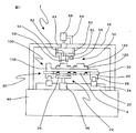
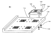
図1は、この発明に係る統合マスクの組立装置の一実施例を示す正面断面図、図2は統合マスクの概略斜視図、図3は図2の統合マスクを各要素ごとに分解した斜視図、図4はこの発明に係る統合マスクの組立装置の別の実施例を示す正面断面図である。
【0014】
図1を参照すると、図2に示す統合マスク100を組み立てる統合マスクの組立装置1がある。ここで統合マスク100は、4つの蒸着マスク120をベース板102に、係合手段140で固定して構成されている。
【0015】
まず蒸着マスク120は、蒸着パターンに応じて蒸着用開口132を配置した開口部130を有するマスクプレート122を、フレーム124に固定して構成される。蒸着マスク120が配置されるベース板102の場所には、図3に示すように開口部130よりも面積が大きく、開口部130がその中に含まれる開口110が必ず設けられている。なお、蒸着用開口132の形状は長方形や円形の穴を多数ならべる等、蒸着パターンにしたがって形成する。
【0016】
さらに蒸着マスク120の各配置位置は、ベース板102の突起部104の上面108に設けられた基準マークであるアライメントマーク106を基準として、蒸着マスク120の所定の蒸着用開口132が定めた位置になるようにしている。ここでは蒸着用開口132の位置を直接検知して、ベース板102上のアライメントマーク106との相対位置合わせを行ってもよいが、各蒸着マスク120のマスク板122にアライメントマーク126を設け、これをベース板102のアライメントマーク106を基準にして位置合わせを行わせるのが好ましい。なお、アライメントマーク106が設けられている突起部104の上面108と蒸着用マスク120のマスクプレート122のベース102からの高さは等しくし、同焦点距離となってカメラによる位置検知が行いやすいようすることが好ましい。
【0017】
係合手段140は、図3を参照すると、押さえ棒142、圧縮バネ144、留め金146より構成されており、押さえ棒142を蒸着用マスク120の取付穴128とベース板102の取付け穴118を通し、ベース板102の裏面で圧縮バネ144を取り付けてから、留め金146を装着して、押さえ棒142が抜けないようにする。これにより、圧縮バネ144の力で蒸着用マスク120をベース板102に一定力で押さえつけて、摩擦力で動かないように保持することになる。また、下側から留め金146を押すと圧縮バネ144が縮み、押さえ棒142の上部の頭部と蒸着用マスク120の間にすきまが生じるので、蒸着用マスク120のベース板102へのおしつけが開放されて、蒸着用マスク120はベース板102上を自在に移動できるようになる。
【0018】
次に再び図1を参照して、統合マスク組立装置1の構成について説明する。統合マスク100は、架台40上に設置されているX−Yテーブル20の支持盤30に載置されている。X−Yテーブル20は支持盤30を、ガイド24とレール22によりX方向(紙面の左右方向)に、ガイド26とレール28によりY方向(紙面に垂直な方向)に移動可能とするので、支持盤30上の統合マスク100を水平面内で自在に移動させることができる。また、支持盤30は統合マスク100のベース板102の周囲のみ保持し、中央部分は開口4となっている。支持盤30のベース板102を保持する部分には複数個の吸着穴が設けられて、ベース板102を吸着保持できる。また、開口4は統合マスク100の直下となり、ここに突き出し板34とエアーシリンダー36よりなる解除ユニット32が収納されるように、配置されている。解除ユニット32のエアーシリンダー36を駆動して突き出し板34を上昇させ、係合手段140の留め金146を突き上げれば、押さえ棒142が統合マスク100の蒸着マスク120から離れ、押しつけが解除されるので、蒸着マスク120をベース板102上で自在に移動させることが可能となる。このように、係合手段140と解除ユニット32は、蒸着マスク120とベース板102の固定・開放を、外力を付加することにより自在に行える係合ユニットの機能を有している。
【0019】
さらに支持盤30に載置されている統合マスク100の直上には、保持ユニット50が、架台40から伸びるフレーム42に吊り下げられる形で配置されている。保持ユニット50は、蒸着マスク120を吸着により保持する吸着パッド52、吸着バッド52を回転させる回転テーブル54、回転テーブル54を支持する支持板56、支持板56を上下方向に昇降させる昇降ユニット60より構成されており、昇降ユニット60がフレーム42と連結して、位置固定されている。昇降ユニット60は図示しない駆動源によって駆動され、その下側にある回転テーブル54と吸着パッド52を自在に昇降させられる。また回転テーブル54はモータ58によって水平面内で回転するとともに、その中央部に円形の開口62を有する。この開口62とその直上にあるフレーム42の開口64を利用して、フレーム42の上部にブラケット68を介して取り付けられたカメラ66で、蒸着マスク等のアライメントマーク位置を検知する。
【0020】
以上の統合マスクの組立装置1を使用した統合マスク100の組立は次のように行う。
【0021】
まず統合マスク100のベース板102の所定位置に各蒸着マスク120を配置し、係合手段140を組み込んで、粗い位置合わせを行う。この下準備を終えたものを統合マスクの組立装置1のX−Yテーブル20の支持盤30にのせ、図示していない真空ポンプを作動させ、統合マスク100のベース板102を吸着保持する。保持方法としては、この他、ボルトによる締結等いかなる手段を用いてもよい。次に、ベース板102上に設けられているアライメントマーク106の位置がカメラ66の真下にくるように、X−Yテーブル20を移動させる。2つのアライメントマーク106をカメラ66で検知することによって、アライメントマーク106の2次元座標値を知ることができる。そしてこれを原点位置とし、これを基に一つの蒸着マスク120のアライメントマーク126があるべき位置を位置Cとすると、その位置Cが、カメラ66の真下にくるようにX−Yテーブルを移動させる。目標位置であるカメラ66の中心位置(画面の十字線の交点)に対して、蒸着マスクのアライメントマーク126がはずれている場合は、次のようにして位置合わせを行う。まず昇降ユニット60を駆動して吸着パッド52を下降させ、直下にある蒸着マスク20と接触させて、蒸着マスク20を吸着する。続いて、解除ユニット32のエアーシリンダー36を上昇させ、突き出し板34で統合マスク100の係合手段140の留め金146を圧縮バネ144の反力に抗して突き上げる。これによって蒸着マスク120のベース板102への固定は解除される。この状態で、アライメントマーク126がカメラ66の中央位置よりもずれている分だけ位置補正するように、回転テーブル54、X−Yテーブル20を駆動して、蒸着マスク120とベース板102との相対距離を変える。そして蒸着マスクの移動が終われば、解除ユニット32のエアーシリンダー36を下降させて、突き出し板34を留め金146から離し、蒸着マスク120をベース板102に圧縮バネ144のバネ力により固定する。づづいて、吸着パッド52の吸着を解除して、昇降ユニット60を上昇させ、吸着パッドを蒸着マスク120から完全に離接させたら、X−Yテーブル20を移動させて、再び蒸着マスク120のアライメントマーク126があるべき位置Cがカメラ66の真下にくるようにして、カメラ66でアライメントマーク126の位置を確認する。そして、アライメントマーク126の位置ずれが許容値内になるまで、上記の蒸着マスクの位置決め作業を繰り返す。
【0022】
以上の方法によって1つの蒸着マスク120の位置決めが完了したら、次の蒸着マスクのアライメントマークがあるべき位置がカメラ66の直下になるようにX−Yテーブル20を移動させ、同じようにアライメントマーク位置の確認、位置決め作業を繰り返す。
【0023】
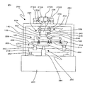
次に図4を参照して、本発明になる別の実施例である統合マスクの組立装置200について説明する。
【0024】
この統合マスクの組立装置200では、統合マスク100は架台260上に設置されているX−Yテーブル202の支持盤204上に載置・保持される。X−Yテーブル202は支持盤204を、ガイド206とレール208によりY方向(紙面に垂直な方向)に、ガイド210とレール212によりX方向(紙面の左右方向)に、移動可能とするので、支持盤204上の統合マスク100を水平面内で自在に移動させることができる。またレール212は、昇降ユニット262を介して架台260に固定されているので、支持盤204は上下方向に昇降も自在に行える。さらに支持盤204は統合マスク100のベース板102の周囲のみ保持し、中央部分は開口214となっている。支持盤204のベース板102を保持する部分には複数個の吸着穴が設けられて、ベース板102を支持盤204に吸着保持できる。また、開口214は統合マスク100の直下となり、ここに突き出し板282とエアーシリンダー284よりなる解除ユニット280が収納されるように、架台260上に配置されている。解除ユニット280のエアーシリンダー284を駆動して突き出し板282を上昇させ、係合手段140の留め金146を突き上げれば、押さえ棒142が統合マスク100の蒸着マスク120から離れ、押しつけが解除されるので、蒸着マスク120をベース板102上で自在に移動させることが可能となる。統合マスクの組立装置200では、係合手段140と解除ユニット280をあわせて、蒸着マスク120とベース板102の固定・開放を、外力を付加することにより自在に行える係合ユニットの機能を有している。
【0025】
さて、統合マスク100の直上には、統合マスク100の蒸着マスク120を保持、移動させる保持ユニット230が配置されている。保持ユニット230は、蒸着マスク120を吸着保持する吸着パッド232と、吸着パッド232に水平面内での回転と、X、Y方向への自在な移動を与える回転テーブル234と上部X−Yテーブル236から構成されている。ここで回転テーブル234は上部X−Yテーブル236に、上部X−Yテーブル236はレール244を介してフレーム250に、それぞれ固定されている。上部X−Yテーブル236は、回転テーブル234に取り付けられているガイド238とレール240によってX方向に、レール240に接続するガイド242とレール244によってY方向に案内される。
【0026】
さらに、回転テーブル234はモータ246で駆動されて水平面内で回転するとともに、その中央部に円形の開口216を有する。この開口216とその直上にあるフレーム250の開口252を利用して、フレーム250の上部に微調整装置272A、Bを介して取り付けられた2つのカメラ270A、Bカメラで、蒸着マスク等のアライメントマーク位置を検知する。微調整装置272A、Bは、カメラ270A、Bの水平、上下方向の位置微調整を自在に行うことができる。
【0027】
以上説明した統合マスクの組立装置200を使用した統合マスク100の組立は次のようにする。
【0028】
まず統合マスク100のベース板102の所定位置に各蒸着マスク120を配置し、係合手段140を組み込んで、粗い位置合わせを行う。この下準備を終えたものを組立装置200のX−Yテーブル202の支持盤204にのせて吸着固定する。次に、ベース板102上に設けられている2つのアライメントマーク106の位置が2つのカメラ270A、Bの真下にくるように、X−Yテーブル202を移動させ、この位置を基準位置Dとする。そしてこの基準位置Dでは、2つのアライメントマーク106がそれぞれ2つのカメラ270A、Bの中央位置(画面の十字線の交点)に合致するように、微調整装置272A、Bを使って、カメラ270A、Bを各々水平面内で移動させる。
【0029】
2つのカメラ270A、Bの位置調整が終了したら、基準位置Dを基点として、統合マスク100の1つの蒸着マスク120のアライメントマーク126があるべき位置にX−Yテーブル202を駆動して、統合マスク100を移動させる。 移動した場所で2つのカメラ270A、Bによって、蒸着マスク120のアライメントマーク126を検知する。検知したアライメントマーク126が2つのカメラ270A、Bの中央位置(画面の十字線の交点)になければ、昇降ユニット262を駆動してX−Yテーブル202を上昇させ、蒸着マスク120を保持ユニット230の吸着パッド232に接触させる。つづいて吸着パッド232に真空ポンプより吸引を行って蒸着マスク120を吸着保持した後に、解除ユニット280のエアーシリンダー284を上昇させて、押さえ板282で統合マスク100の係合手段140の留め金146をバネ144の反力に抗して突き上げる。これによって蒸着マスク120のベース板102への固定は解除される。この状態で、アライメントマーク126が2つのカメラ270A、Bの中央位置(十字線の交点)に来るように、回転テーブル234と上部X−Yテーブル236を駆動して、回転と水平移動により蒸着マスク120をベース板102上で移動させる。カメラ270A、Bにより、アライメントマーク126が所定位置に位置決めできているのを確認できたら、解除ユニット280のエアーシリンダー284を下降させて、押さえ板282を留め金146から離して、蒸着マスク120をベース板102に固定する。そして、吸着パッド232の吸着を停止してから、昇降ユニット262を下側に駆動してX−Yテーブル202を下降させ、吸着パッド232と蒸着マスク120を離間させる。続いて次の位置決めすべき蒸着マスク120について、同じ位置決め作業をくり返す。
【0030】
上記の位置決め作業で、位置決め作業完了と判断するアライメントマークのあるべき位置との許容ずれ量は、好ましくは1〜100μm、より好ましくは1〜20μmにする。また、吸着パッドによる蒸着マスク120の吸着力、支持盤とベース板102の吸着力は、好ましくは0.1〜50kPa、より好ましくは、5〜20kPaとする。なお、蒸着マスク120をベース板102上で相対移動させて位置決めする手段としては、吸着パッドを使用せずに、単に蒸着マスク120を部材で押し付けて摩擦力により、蒸着マスクをベース板102上で相対移動させてもよいし、エアーを噴出して吸引する把持装置により蒸着マスクをベース板102上で相対移動させてもよい。
【0031】
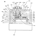
次に図5を参照して、本発明のさらに別の態様である統合マスクの組立装置300について説明する。ここで図5は統合マスクの組立装置300の正面断面図、図6は、組立装置300により組立が行われる組立マスク400の概略斜視図である。
【0032】
図5の統合マスクの組立装置300は、図6に示す統合マスク400を精度よく組み立てることができるものである。ここで、統合マスク400は、4つの蒸着マスク420を、ベース板402の中央に設けた突起部404の上面408にある十字形状のアライメントマーク406を基準として、突起部404の両隣の位置に、係合手段440で耳部428を固定して配置されている。蒸着マスク420自体は、蒸着用の開口432を配した開口部430と十字形状のアライメントマーク426を有するマスクプレート422を、フレーム424に固定して構成されている。蒸着マスク420上の2つのアライメントマーク426の間隔は、ベース板402上の2つのアライメントマーク406の間隔と一致させている。さらに蒸着マスク420の真下のベース板402上には、蒸着物が開口部430に達するように図示しない開口が設けられている。また、係合手段440は、押さえ板442、押さえ板442を軸448の回りに回転自在に保持する保持台446、押さえ板446の一端を押し上げる圧縮バネ444より構成されている。そして圧縮バネ444により押さえ板442の一端を押し上げる力により、押さえ板442の反対側の端部の真下にある蒸着マスク420の耳部428を一定力で押さえることになり、この時に発生する摩擦力により蒸着マスク420がベース板402に固定される。またベース板402の蒸着マスク420を載せる反対面(裏面)には、図示しない穴が設けられている。この穴は、統合マスクの組立装置300の支持盤304上にあるピン314と係合して、支持盤304上でベース板402が移動しないように固定するためのものであり、少なくとも2個以上設ける。
【0033】
さて図5を見ると、統合マスクの組立装置300は、図4に示す統合マスクの組立装置200の解除ユニット280、保持ユニット230、支持盤204を、別の解除ユニット380、保持ユニット330、支持盤304に置き換えたのと、昇降ユニット262を除去し、上部X−Yテーブル236を共通プレート392を介してエアーシリンダー390で昇降可能にしただけであるので、置き換えた部分の構成だけを説明する。
【0034】
まず、解除ユニット380は、突き出し板382と、突き出し板382を上下に移動させるエアーシリンダー384よりなり、エアーシリンダー384の上部がフレーム250に固定されている。エアーシリンダー384を駆動して突き出し板382を下降させると、先端部386が統合マスク400の係合手段440の押さえ板442の圧縮バネ444上方部分を押さえるので、押さえ板442の片端が蒸着マスク420の耳部428より離れ、蒸着マスク420がベース板402上を自在に移動できるようになる。エアーシリンダー384を上昇させると、先端部386が押さえ板442から離れ、圧縮バネ444の作用により、押さえ板442の片端は再び耳部428を押さえつけるので、蒸着マスク420はベース板402に固定されることになる。以上の解除ユニット380と、統合マスク400の係合手段440をあわせて、蒸着マスク420とベース板402の固定・開放を、外力付加により自在に行える係合ユニットの機能を有する。
【0035】
次に保持ユニット330は、図4の統合マスクの組立装置200の保持ユニット230の内で、吸着パッド232だけを、統合マスク400上の蒸着マスク420を4側面から挟み込んで保持する把持ピン332に置き換えただけである。把持ピンは332は、回転テーブル234による回転と、上部X−Yテーブル236によるX、Y方向への移動を、自在に行うことができる。また、把持ピン332はエアーシリンダー390288により、上部X−Yテーブル236と共に上下にも自在に移動可能である。
【0036】
さらに支持盤304の上面には、図4の統合マスクの組立装置200の支持盤204とは異なり、ピン314(破線で図示)が設けられている。このピンは上記したように、統合マスク400のベース板402の裏面にある穴と係合する位置にあり、ベース板を支持盤304上で固定する。
【0037】
次に、統合マスクの組立装置300を使用した統合マスク400の組立は次のようにして行う。
【0038】
まず統合マスク400のベース板402の所定位置に、4つの各蒸着マスク420を配置し、各々の蒸着マスク420の耳部428を係合手段440の押さえ板442で、圧縮バネ444による一定力にて押さえ込んで固定し、粗い位置合わせを行う。この下準備を終えたものを組立装置300のX−Yテーブル202の支持盤304にのせて、ピン314をベース板402の裏面にある図示しない穴と係合させて、統合マスクを支持盤304上で固定する。
【0039】
次に、ベース板402の突起部404上に設けられている2つのアライメントマーク406の位置が2つのカメラ270A、Bの真下にくるように、X−Yテーブル202を移動させ、この位置を基準位置Eとする。そしてこの基準位置Eでは、2つのアライメントマーク406がそれぞれ2つのカメラ270A、Bの中央位置(画面の十字線の交点)に合致するように、微調整装置272A、Bを使って、カメラ270A、Bを各々水平面内で移動させる。
【0040】
2つのカメラ270A、Bの位置調整が終了したら、基準位置Eを基点として、統合マスク400の1つの蒸着マスク420のアライメントマーク426があるべき位置にX−Yテーブル202を駆動して、統合マスク400を移動させる。移動した場所で2つのカメラ270A、Bによって、蒸着マスク420のアライメントマーク426を検知する。検知したアライメントマーク426の十字形の交点が2つのカメラ270A、Bの中央位置(画面の十字線の交点)になければ、エアーシリンダー390を駆動して把持ピン332を下降させ、把持ピン332で蒸着マスク420の4側面を挟み込んで保持する。つづいて、解除ユニット380のエアーシリンダー384を駆動して、突き出し板382を下降させ、蒸着マスク420をベース板402上で固定している係合手段440の押さえ板442の片端を、突き出し板382の先端部386で押し込んで、押さえ板442の端部を蒸着マスク420の耳部428から引き離し、蒸着マスク420をベース板402上で移動自在にする。この把持ピン332で蒸着マスク420を保持した状態で、蒸着マスク420上のアライメントマーク426が2つのカメラ270A、Bの中央位置(十字線の交点)に来るように、回転テーブル234と上部X−Yテーブル236を駆動して、回転と水平移動により蒸着マスク420をベース板402上で移動させる。カメラ270A、Bにより、アライメントマーク426が所定位置に位置決めできていることを確認できたら、解除ユニット380のエアーシリンダー384を上昇させて、突き出し板382の先端部386を押さえ板442の片端から離して、圧縮バネ444の作用により、再び蒸着マスク420をベース板402に固定する。そして、シリンダー390を駆動して、把持ピン332を上昇させて、把持ピン332による蒸着マスク420の保持を解除する。続いて次の位置決めすべき蒸着マスク420について、同じ位置決め作業をくり返す。
【0041】
上記の位置決め作業で、位置決め作業完了と判断するアライメントマークのあるべき位置との許容ずれ量は、好ましくは1〜100μm、より好ましくは1〜20μmにする。
【0042】
さらに上記の実施態様では、把持ピン332が蒸着マスク420を把持するときに、把持ピン332と蒸着マスク420の4側面との間には、小さな隙間が発生する。この隙間は好ましくは0.1から5mm、より好ましくは0.5から1mmにする。また、チャック機構を付加して、把持ピン332で蒸着マスクの4側面を、隙間なく一定力で把持するようにしてもよい。
【0043】
【実施例】
実施例1
発光層用の蒸着マスク用のプレートとして、外形が84mm幅×105mm長で厚さが25μmのNi合金を用意した。幅100μmで長さが64mmの長方形開口を、開口の長手方向(64mmの方向)がプレートの幅方向(84mmの方向)と一致するようにして、ピッチ300μmでプレートの長手方向に272個設けた。なお長方形開口はプレートの長手、幅方向ともプレートの中央になるようにし、さらに長手方向の上側端部より5mmの直線上に、幅方向に対称となるようにピッチ30mmで十字形状のアライメントマークを2個設けて、蒸着マスクプレートを作成した。同様にして同じ蒸着マスクプレートを16個作成した。
【0044】
この蒸着マスクプレートを、全体の大きさが104mm幅×105mm長でステンレス製の図2のフレーム124の長手方向中央部にある外形が84mm幅×105mm長の取り付け部に接着によりとりつけ、蒸着マスクを作成した。同様に同じ蒸着マスクを16個作成した。なお蒸着マスクのフレーム124のマスクプレート取り付け部は、厚さ10mmで、外形から4mmを接着代として残して、その内側は76mm幅×97mm長の開口とした。またフレーム24の幅方向の両端10mmは厚さ5mmで、固定用のφ5mmの穴を片側2ヶ所づつ、合計4ヶ所設けた。
【0045】
次に441mm幅×455mm長で厚さ5mmのアルミ板に、76mm幅×95mm長の開口を、幅方向に左端部より19mmの位置のところから109mmピッチで4列、長手方向に上端部より20mmの位置から110mmピッチで4列の合計16個設けたものを、図2のベース板102とした。そして、それに上記の蒸着マスク16個を、各々の蒸着マスクの開口がベース板2の開口の中央になるように配置した。さらに蒸着マスク1個に対して4本の係合手段140を使用して各蒸着マスクをベース板に固定し、粗い位置合わせを行った統合マスクを作成した。なおベース板の長手方向上部端部10mmは厚さ15mmとなっており、その上面にアライメントマークとして直径1mmで深さ5mmの穴を幅方向の中央部に30mmのピッチで、上部端部より5mmの位置に中心がくるように2個設けた。アライメントマークのある面は、ベース板に取り付けた蒸着マスク120の上面と同じ高さになった。また係合ユニットはステンレス製で、押さえ棒142の頭部は直径8mm、ベース板の穴に貫通させる部分は直径4mmであり、圧縮バネ44にはバネ定数10N/mmのものを使用して、一個の蒸着マスクを100Nの力でベース板に押し付けるようにした。
【0046】
次に、上記の粗い位置あわせを行った統合マスクを図1の統合マスク組立装置1の支持盤30に取り付け、ベース板上の16個の蒸着マスクの位置を、アライメントマークのずれが5μm以下になるように調整した。なお統合マスク組立装置で、X−Yテーブル20は1μm単位で平面内で移動可能とし、回転テーブルは0.001度の単位で回転できるようにした。さらに吸着パッドには直径30mmの樹脂製多孔質のものを使用して、1〜50kPaの吸引力をもたせるようにした。また支持盤30は外形が500mm×500mmで中央に400mm幅×415mm長の開口があり、さらに表面に直径2mmの穴を吸引孔として、20mmピッチで設け、ベース板102を1〜50kPaの吸引力で吸引できるようにした。またカメラ66には1μmの分解能をもつCCDカメラを用い、画像処理装置によって位置ずれ量や、補正量の計算を行った。また解除ユニット32のエアーシリンダー36には0.5MPaの圧空を供給し、蒸着マスクの位置調整中には係合手段140を解除した。作成した統合マスクは、蒸着マスクの所定位置からの位置ずれ量が、16個とも5μm以下となり、初期の目標のものを作成できた。
【0047】
実施例2
実施例1で作成した統合マスク100を緑色発光層用として、緑色発光層用蒸着装置のマスクホルダーに装着した。そして緑色発光層用統合マスクの蒸着マスクプレート上の100μm幅×64mm長の開口の全ての位置を、プレート長手方向に100μm(1ピッチ分)だけをずらす他は、実施例1と全く同じにして赤色発光層用統合マスクを作成するとともに、緑色発光層用統合マスクの蒸着マスクプレート上の100μm幅×64mm長の開口の全ての位置を、プレート長手方向に200μm(2ピッチ分)だけをずらす他は、実施例1と全く同じにして青色発光層用統合マスクを作成した。
【0048】
次に、厚さ1.1mmで外形が457mm幅×455mm長の無アルカリガラス表面にITO透明電極膜を130nmだけスパッタリングにて全面形成した。ここで基板幅方向に並行して長さが90mm、幅が70μmのストライプ形状を16個の有機EL素子に対応して形成できるよう、フォトリソ法によって、第1電極を形成した。
【0049】
続いて本基板上全面にポジ型フォトレジスト(東京応化(株)製、OFPR−800)をスピナーにより厚さ3μmになるように塗布した。乾燥後この塗布膜にフォトマスクを介して露光、現像してフォトレジストのパターニングを行った後、180℃でキュアを行って、16個の有機EL素子の有効発光エリア(第1電極と後のR、G、B発光層が占める領域)を全面を覆うように、それぞれに対応して16単位のスペーサを形成した。
【0050】
次に16個ある有機EL素子の有効発光エリア全面に、銅フタロシアニンを15nm、ビス(N−エチルカルバゾール)を60nmを蒸着して、正孔輸送層を形成した。蒸着時の真空度は2×10⁻⁴Pa以下とし、蒸着中は基板を蒸着源に対して回転させた。
【0051】
次に発光層を蒸着するために、蒸着装置に緑色発光層用統合マスクを装着し、つづいて基板ホルダーから正孔輸送層まで蒸着したガラス基板を緑色発光層用統合マスク上に載置した。ついで真空ポンプを駆動して、蒸着槽内の真空度を1×10⁻⁴Paにした。所定の真空度がえられてから、基板および統合マスクに形成されたアライメントマークで位置合わせを行った。位置合わせ完了後、ガラス基板を緑色発光層用統合マスクに20Nの力で押し付けた。つづいて蒸着源を加熱し、緑色発光層として、0.3wt%の1,3,5,7,8,−ペンタメチル−4,4−ジフロロ−4−ボラ−3a,4a−ジアザ−s−インダセン(PM546)をドーピングした8−ヒドロキシキノリン−アルミニウム錯体(Alq3)を、統合マスクのパターンにしたがって20nm蒸着した。
【0052】
次に蒸着された基板を取り出し、赤色発光層用統合マスクが装着されている別の蒸着装置に移載し、緑色発光層の場合と同じく基板と統合マスクの位置合わせを行った後、1×10⁻⁴Paの真空下で赤色発光層として1wt%の4−(ジシアノメチレン)−2−メチル−6(ジュロリジルスチリル)ピラン(DCJT)をドーピングしたAlq3を15nm蒸着した。つづいて、基板を青色発光層用統合マスクが装着されているさらにまた別の蒸着装置に移載し、同様に基板と統合マスクの位置合わせを行った後、1×10 −4 Paの真空下で青色発光層として4,4’−ビス(2,2−ジフェニルビニル)ジフェニル(DPVBi)を20nm蒸着した。
【0053】
この発光層はストライプ状の第1電極に各々対応しており、第1電極の露出部分を完全に被覆した。
【0054】
次にDPVBiを45nm、Alq3を10nm、16個ある有機EL素子の有効発光エリア全面に蒸着した。つづいて、基板長手方向(第1電極に直交する方向)に長さ100mm、基板幅方向に250μmで厚さ240nmであるアルミニウムのストライプを、基板幅方向にピッチ300μmで200本配置したストライプ列を1単位とし、これを先に作成した基板上のスペーサの開口部を覆うように幅方向ピッチ109mm、基板長手方向ピッチ110mmで16単位配置できるようアルミニウムの蒸着を行い、第2電極を形成した。なお蒸着時の真空度は3×10⁻⁴Pa以下とした。そして最後に一酸化珪素を200nmの厚さに電子ビーム蒸着法によって全面蒸着し、保護層を形成した。
【0055】
以上のようにして16個の発光素子が形成された基板を切断して、16個の発光素子に分割した。各々の発光素子には、816本のITOストライプ状第1電極上にパターニングされたRGBそれぞれの発光層を含む薄膜層と、さらに第1電極と直交するするように200本のストライプ状第2電極が形成された。第1、第2電極の交差部分のうちスペーサーの開口部のみが発光し、RGB各1つずつの発光単位が1画素を形成するので、300μmピッチで272×200画素を有する単純マトリックス型カラー有機EL素子が製作できた。製作した有機EL素子の発光性能はディスプレイとして使用できるものであった。また蒸着マスクを分割して発光層を蒸着したので、16個全て同一寸法精度と性能をもつ発光素子を製作することができた。
【0056】
なお、本発明の組立装置および組立方法は、発光層用の統合マスクにも第2電極用のそれにも適用可能である。製作される有機EL素子は単純マトリックス型でもアクティブマトリックス型でもよく、また、モノクロタイプでもよい。
【0057】
【発明の効果】
本発明になる統合マスクの組立装置および組立方法によれば、統合マスクを構成するベース板と蒸着マスクの位置を検知して、両者の相対位置決めを行うのであるから、高い精度に統合マスクに組み立てることが可能となる。
【0058】
高精度の統合マスクの組立は、蒸着マスクの個数が多くなっても可能であるので、一枚の基板に多数の有機EL素子を製作する、いわゆる多面取り用の蒸着マスクにも適用することができる。これによって、多面取りの場合でも、発光層や第1電極層の位置決めが高精度である高品質の有機EL素子を、高い収率で製造することが可能となる。
【図面の簡単な説明】
【図1】本発明に係る統合マスクの組立装置の一実施例を示す正面断面図。
【図2】統合マスクの概略斜視図。
【図3】図2の統合マスクを各要素ごとに分解した斜視図。
【図4】本発明に係る統合マスクの組立装置の別の実施例を示す正面断面図。
【図5】本発明に係る統合マスクの組立装置のさらに別の実施例を示す正面断面図。
【図6】統合マスクの別の実施例を示す概略斜視図。
【符号の説明】
1 統合マスクの組立装置
20 X−Yテーブル
30 支持盤
32 解除ユニット
40 架台
42 フレーム
50 保持ユニット
52 吸着パッド
54 回転テーブル
60 昇降ユニット
62 開口
66 カメラ
100 統合マスク
102 ベース板
106 アライメントマーク
110 開口
120 蒸着マスク
122 マスクプレート
130 開口部
140 係合手段
142 押さえ棒
144 圧縮バネ
146 留め金
200 統合マスクの組立装置
202 X−Yテーブル
204 支持盤
230 保持ユニット
232 吸着パッド
234 回転テーブル
236 上部X−Yテーブル
250 フレーム
260 架台
262 昇降ユニット
270A、B カメラ
272 微調整装置
280 解除ユニット
300 統合マスクの組立装置
304 支持盤
314 ピン
330 保持ユニット
332 把持ピン
380 解除ユニット
382 突き出し板
384 エアーシリンダー
386 先端部
390 エアーシリンダー
392 共通プレート
400 統合マスク
402 ベース板
404 突起部
406 アライメントマーク
420 蒸着マスク
422 マスクプレート
426 アライメントマーク
428 耳部
430 開口部
432 開口
440 係合手段
442 押さえ板
444 圧縮バネ
446 保持台
448 軸[0001]
BACKGROUND OF THE INVENTION
In order to manufacture an organic EL element capable of converting electric energy into light, which can be used in the fields of display elements, flat panel displays, backlights, lighting, interiors, signs, signboards, electrophotographic machines, etc. The present invention relates to an evaporation mask assembling apparatus and assembling method to be used, and an organic EL element manufacturing method using the same.
[0002]
[Prior art]
The organic EL element is based on the principle that electrons injected from the cathode and holes injected from the anode are recombined in an organic phosphor sandwiched between the two electrodes to emit light, and has a simple structure and low voltage. Since it can emit multi-color light with high brightness, it has begun to be widely used for thin and small displays.
[0003]
In order to produce a full-color display panel using this organic EL element, the first and second electrodes in addition to the red (R), green (G), and blue (B) light emitting layers as constituent elements on the substrate. It is necessary to arrange the layers regularly with a predetermined pattern and pitch.
[0004]
Among the above thin film layers, in order to form an organic thin film layer to be a light emitting layer in a highly accurate fine pattern, from the characteristics of the organic thin film, using a mask having an opening arrangement corresponding to the arrangement pattern of the light emitting layer, A mask vapor deposition method in which vapor deposition is performed under vacuum is usually used.
[0005]
[Problems to be solved by the invention]
In order to improve the productivity of the above-mentioned organic EL element manufacturing, the mask vapor deposition used for forming the light emitting layer becomes a batch process for each substrate, and the current organic EL element has many small applications, so one sheet So-called multi-sided forming, in which a large number of organic EL elements are formed on a large substrate, is effective. In order to obtain multiple surfaces, it is necessary to create a vapor deposition mask having a large number of aperture arrangement portions corresponding to the size of one organic EL element. However, since such a vapor deposition mask is enlarged and greatly deformed during manufacture and use, and the dimensional accuracy of the opening array portion cannot be maintained with high accuracy, Japanese Patent Application Laid-Open No. 2000-113978 corresponds to one organic EL element. There is shown a means for maintaining a high dimensional accuracy by introducing a gathering type vapor deposition mask (integrated mask) in which a large number of one vapor deposition mask having an opening arrangement is arranged. The light emitting layer has three colors of RGB, and the positioning of the vapor deposition mask between the respective light emitting layers is important. Therefore, in the case of an assembling type vapor deposition mask, that is, an integrated mask, there are a number of individual vapor deposition masks corresponding to multi-cavity. It is essential to accurately position the position at a predetermined position. However, nothing is shown about means for assembling such an integrated mask with high accuracy.
[0006]
The present invention has been made based on the above-described circumstances, and an object of the present invention is to provide means for positioning a large number of vapor deposition masks at predetermined positions with high accuracy and assembling the integrated mask in the integrated mask. An object of the present invention is to provide an organic EL device manufacturing method capable of dramatically improving productivity by forming a large number of organic EL devices on a single substrate using the integrated mask thus prepared.
[0007]
The above objective is accomplished by the present invention. That is, according to the present invention, a plurality of vapor deposition masks having a vapor deposition opening array corresponding to the vapor deposition pattern are arranged on the base plate, and the vapor deposition mask is used as the base plate.With the force of the compression springAn apparatus for assembling an integrated mask having engaging means for pressing and holding by frictional force, a table for holding the base plate, a vapor deposition mask, and freely movable relative to the base plate A vapor deposition mask holding and moving mechanism, a positioning system for detecting a reference mark or a reference position of the base plate and the vapor deposition mask, and performing relative positioning between the vapor deposition mask and the base plate using the vapor deposition mask holding and moving mechanism, and the engagement An integrated mask assembling apparatus comprising a releasing unit that releases pressing by means and allows the deposition mask to freely move on the base plate, and is an integrated mask assembling method using this apparatus. Furthermore, it is a manufacturing method of the organic EL element using the integrated mask obtained from the assembly method.
[0008]
DETAILED DESCRIPTION OF THE INVENTION
An integrated mask assembling apparatus according to the present invention is an integrated mask assembling apparatus configured by arranging and fixing a plurality of vapor deposition masks having a vapor deposition opening array corresponding to a vapor deposition pattern on a base plate. A vapor deposition mask holding / moving mechanism that holds the vapor deposition mask and can be freely moved relative to the base plate, and detects the reference mark or reference position of the base plate and the vapor deposition mask to hold the vapor deposition mask. A positioning system that performs relative positioning of the vapor deposition mask and the base plate using a moving mechanism, and an engagement unit that fixes and releases the vapor deposition mask and the base plate are provided.
[0009]
An integrated mask assembling method of the present invention is an integrated mask assembling method configured by arranging and fixing a plurality of vapor deposition masks having vapor deposition openings corresponding to vapor deposition patterns on a base plate, Hold the base plate on the table with the deposition mask placed on it, detect the reference mark or reference position of the base plate and the deposition mask, and hold the deposition mask relative to the base plate and the deposition mask. Then, after the positioning is completed, the vapor deposition mask and the base plate are fixed by the engagement unit.
[0010]
The organic EL device manufacturing method of the present invention is characterized in that an organic EL device is manufactured by depositing a thin film layer using the integrated mask assembled by the integrated mask assembling method of the present invention.
[0011]
According to the integrated mask assembling apparatus and the assembling method of the present invention, since the positions of the base plate and the vapor deposition mask are detected and the relative positioning of the two is performed, the integrated mask can be assembled with high accuracy.
[0012]
According to the method for manufacturing an organic EL element of the present invention, a thin film layer such as a light emitting layer is deposited using an integrated mask accurately manufactured by the above assembly apparatus and assembly method. So-called multi-planar forming of a large number of organic EL elements can be performed with high pattern accuracy, and high-quality organic EL elements can be obtained with high productivity.
[0013]
Hereinafter, a preferred embodiment of the present invention will be described with reference to the drawings.
FIG. 1 is a front sectional view showing an embodiment of an integrated mask assembling apparatus according to the present invention, FIG. 2 is a schematic perspective view of the integrated mask, and FIG. 3 is a perspective view in which the integrated mask of FIG. FIG. 4 is a front sectional view showing another embodiment of the integrated mask assembling apparatus according to the present invention.
[0014]
Referring to FIG. 1, there is an integrated mask assembly apparatus 1 for assembling the integrated
[0015]
First, the
[0016]
Furthermore, each arrangement position of the
[0017]
Referring to FIG. 3, the engaging means 140 includes a
[0018]
Next, the configuration of the integrated mask assembling apparatus 1 will be described with reference to FIG. 1 again. The
[0019]
Further, a holding
[0020]
The assembly of the
[0021]
First, each
[0022]
When the positioning of one
[0023]
Next, an integrated
[0024]
In the integrated
[0025]
Now, a holding
[0026]
Further, the rotary table 234 is driven by a
[0027]
The assembly of the
[0028]
First, each
[0029]
When the position adjustment of the two
[0030]
In the positioning operation described above, the allowable deviation from the position where the alignment mark is to be determined, which is determined to be the completion of the positioning operation, is preferably 1 to 100 μm, more preferably 1 to 20 μm. The suction force of the
[0031]
Next, an integrated
[0032]
The integrated
[0033]
Referring now to FIG. 5, the integrated
[0034]
First, the
[0035]
Next, in the holding
[0036]
Further, unlike the
[0037]
Next, assembling of the
[0038]
First, each of the four vapor deposition masks 420 is disposed at a predetermined position of the
[0039]
Next, the XY table 202 is moved so that the positions of the two
[0040]
When the position adjustment of the two
[0041]
In the positioning operation described above, the allowable deviation from the position where the alignment mark is to be determined, which is determined to be the completion of the positioning operation, is preferably 1 to 100 μm, more preferably 1 to 20 μm.
[0042]
Further, in the above embodiment, when the holding
[0043]
【Example】
Example 1
A Ni alloy having an outer shape of 84 mm width × 105 mm length and a thickness of 25 μm was prepared as a deposition mask plate for the light emitting layer. 272 rectangular openings having a width of 100 μm and a length of 64 mm were provided in the longitudinal direction of the plate at a pitch of 300 μm so that the longitudinal direction of the opening (direction of 64 mm) coincided with the width direction of the plate (direction of 84 mm). . The rectangular opening should be at the center of the plate in both the longitudinal and width directions, and a cross-shaped alignment mark should be placed on the straight line 5 mm from the upper end in the longitudinal direction at a pitch of 30 mm so as to be symmetrical in the width direction. Two deposition mask plates were prepared. Similarly, 16 identical deposition mask plates were prepared.
[0044]
The vapor deposition mask plate is attached to an attachment portion having an overall size of 104 mm width × 105 mm length and a
[0045]
Next, on a 441 mm wide x 455 mm long and 5 mm thick aluminum plate, 76 mm wide x 95 mm long openings, 4 rows at a 109 mm pitch from a position 19 mm from the left end in the width direction, and 20 mm from the top end in the longitudinal direction. A total of 16 columns in four rows at a pitch of 110 mm from the position No. 1 were used as the
[0046]
Next, the integrated mask subjected to the above rough alignment is attached to the
[0047]
Example 2
The
[0048]
Next, an ITO transparent electrode film was formed on the entire surface by sputtering on an alkali-free glass surface having a thickness of 1.1 mm and an outer shape of 457 mm width × 455 mm length by sputtering. Here, the first electrode was formed by a photolithography method so that a stripe shape having a length of 90 mm and a width of 70 μm could be formed corresponding to the 16 organic EL elements in parallel with the substrate width direction.
[0049]
Subsequently, a positive photoresist (manufactured by Tokyo Ohka Kogyo Co., Ltd., OFPR-800) was applied to the entire surface of the substrate with a spinner to a thickness of 3 μm. After drying, this coating film is exposed and developed through a photomask and patterned to form a photoresist, and then cured at 180 ° C. to obtain effective light-emitting areas of the 16 organic EL elements (the first electrode and the subsequent electrodes). In order to cover the entire surface (regions occupied by the R, G, and B light emitting layers), 16 units of spacers were formed corresponding to each.
[0050]
Next, 15 nm of copper phthalocyanine and 60 nm of bis (N-ethylcarbazole) were vapor-deposited on the entire effective light emitting area of the 16 organic EL elements to form a hole transport layer. Degree of vacuum during deposition is 2 × 10-FourThe pressure was set to Pa or less, and the substrate was rotated with respect to the vapor deposition source during the vapor deposition.
[0051]
Next, in order to deposit the light emitting layer, the green light emitting layer integrated mask was attached to the vapor deposition apparatus, and the glass substrate deposited from the substrate holder to the hole transport layer was placed on the green light emitting layer integrated mask. Next, the vacuum pump is driven, and the degree of vacuum in the vapor deposition tank is 1 × 10.-FourPa. After a predetermined degree of vacuum was obtained, alignment was performed using alignment marks formed on the substrate and the integrated mask. After the alignment was completed, the glass substrate was pressed against the green light emitting layer integrated mask with a force of 20N. Subsequently, the vapor deposition source was heated to form 0.3 wt% of 1,3,5,7,8, -pentamethyl-4,4-difluoro-4-bora-3a, 4a-diaza-s-indacene as a green light emitting layer. An 8-hydroxyquinoline-aluminum complex (Alq3) doped with (PM546) was deposited to 20 nm according to the pattern of the integrated mask.
[0052]
Next, the vapor-deposited substrate is taken out, transferred to another vapor deposition apparatus equipped with an integrated mask for the red light emitting layer, and after aligning the substrate and the integrated mask as in the case of the green light emitting layer, 1 × 10⁻⁴Alq3 doped with 1 wt% 4- (dicyanomethylene) -2-methyl-6 (julolidylstyryl) pyran (DCJT) was deposited as a red light emitting layer under a vacuum of Pa by 15 nm. Subsequently, the substrate was transferred to yet another vapor deposition apparatus equipped with the blue light emitting layer integrated mask, and after the substrate and the integrated mask were similarly aligned, 1 × 10 -4 Under a vacuum of Pa, 4,4′-bis (2,2-diphenylvinyl) diphenyl (DPVBi) was deposited as a blue light-emitting layer by 20 nm.
[0053]
The light emitting layers correspond to the striped first electrodes, respectively, and completely cover the exposed portions of the first electrodes.
[0054]
Next, DPVBi was deposited at 45 nm, Alq3 was deposited at 10 nm, and the entire surface of the effective light emitting area of 16 organic EL elements was deposited. Subsequently, a stripe row in which 200 aluminum stripes having a length of 100 mm in the substrate longitudinal direction (direction orthogonal to the first electrode), 250 μm in the substrate width direction and 240 nm in thickness are arranged at a pitch of 300 μm in the substrate width direction is provided. One unit was formed, and aluminum was vapor-deposited so that 16 units could be arranged at a width direction pitch of 109 mm and a substrate longitudinal direction pitch of 110 mm so as to cover the opening of the spacer on the previously prepared substrate, thereby forming a second electrode. The degree of vacuum during deposition is 3 × 10.-FourIt was set to Pa or less. Finally, silicon monoxide was deposited on the entire surface by an electron beam deposition method to a thickness of 200 nm to form a protective layer.
[0055]
The substrate on which 16 light emitting elements were formed as described above was cut and divided into 16 light emitting elements. Each light emitting element includes a thin film layer including RGB light emitting layers patterned on 816 ITO striped first electrodes, and 200 striped second electrodes orthogonal to the first electrodes. Formed. Of the intersecting portions of the first and second electrodes, only the opening of the spacer emits light, and each of R, G, and B forms one pixel, so that a simple matrix type color organic having 272 × 200 pixels at a pitch of 300 μm. An EL element was produced. The light emitting performance of the manufactured organic EL device was usable as a display. Further, since the light emitting layer was vapor deposited by dividing the vapor deposition mask, all 16 light emitting elements having the same dimensional accuracy and performance could be manufactured.
[0056]
Note that the assembling apparatus and assembling method of the present invention can be applied to both the integrated mask for the light emitting layer and that for the second electrode. The organic EL element to be manufactured may be a simple matrix type, an active matrix type, or a monochrome type.
[0057]
【The invention's effect】
According to the integrated mask assembling apparatus and the assembling method according to the present invention, the positions of the base plate and the vapor deposition mask constituting the integrated mask are detected and the relative positioning of the two is performed. Therefore, the integrated mask is assembled with high accuracy. It becomes possible.
[0058]
Assembling a high-precision integrated mask is possible even when the number of vapor deposition masks increases, so it can be applied to so-called multi-surface vapor deposition masks that produce a large number of organic EL elements on a single substrate. it can. As a result, even in the case of multi-planarization, it is possible to manufacture a high-quality organic EL element with high accuracy in positioning the light emitting layer and the first electrode layer with high yield.
[Brief description of the drawings]
FIG. 1 is a front sectional view showing an embodiment of an integrated mask assembling apparatus according to the present invention.
FIG. 2 is a schematic perspective view of an integrated mask.
FIG. 3 is an exploded perspective view of each element of the integrated mask of FIG.
FIG. 4 is a front sectional view showing another embodiment of the integrated mask assembling apparatus according to the present invention.
FIG. 5 is a front sectional view showing still another embodiment of the integrated mask assembling apparatus according to the present invention.
FIG. 6 is a schematic perspective view showing another embodiment of an integrated mask.
[Explanation of symbols]
1 Integrated mask assembly equipment
20 XY table
30 Supporting plate
32 Release unit
40 frame
42 frames
50 Holding unit
52 Suction pad
54 Rotating table
60 Lifting unit
62 Opening
66 Camera
100 integrated mask
102 Base plate
106 Alignment mark
110 opening
120 Deposition mask
122 Mask plate
130 opening
140 engaging means
142 presser bar
144 Compression spring
146 clasp
200 Integrated mask assembly equipment
202 XY table
204 Supporting board
230 Holding unit
232 Suction pad
234 rotating table
236 Upper XY table
250 frames
260 frame
262 Lifting unit
270A, B camera
272 Fine adjustment device
280 Release unit
300 Integrated mask assembly equipment
304 Supporting plate
314 pin
330 Holding unit
332 Grip pin
380 Release unit
382 Extrusion board
384 Air cylinder
386 Tip
390 Air cylinder
392 Common plate
400 integrated mask
402 Base plate
404 Protrusion
406 Alignment mark
420 Deposition mask
422 Mask plate
426 Alignment mark
428 Ear
430 opening
432 opening
440 engagement means
442 holding plate
444 Compression spring
446 holding stand
448 axes
Claims (3)
Priority Applications (1)
| Application Number | Priority Date | Filing Date | Title |
|---|---|---|---|
| JP2002022983A JP4096568B2 (en) | 2001-01-31 | 2002-01-31 | Integrated mask assembling apparatus and assembling method, and organic EL element manufacturing method. |
Applications Claiming Priority (3)
| Application Number | Priority Date | Filing Date | Title |
|---|---|---|---|
| JP2001023475 | 2001-01-31 | ||
| JP2001-23475 | 2001-01-31 | ||
| JP2002022983A JP4096568B2 (en) | 2001-01-31 | 2002-01-31 | Integrated mask assembling apparatus and assembling method, and organic EL element manufacturing method. |
Publications (3)
| Publication Number | Publication Date |
|---|---|
| JP2002305081A JP2002305081A (en) | 2002-10-18 |
| JP2002305081A5 JP2002305081A5 (en) | 2005-08-11 |
| JP4096568B2 true JP4096568B2 (en) | 2008-06-04 |
Family
ID=26608626
Family Applications (1)
| Application Number | Title | Priority Date | Filing Date |
|---|---|---|---|
| JP2002022983A Expired - Fee Related JP4096568B2 (en) | 2001-01-31 | 2002-01-31 | Integrated mask assembling apparatus and assembling method, and organic EL element manufacturing method. |
Country Status (1)
| Country | Link |
|---|---|
| JP (1) | JP4096568B2 (en) |
Families Citing this family (3)
| Publication number | Priority date | Publication date | Assignee | Title |
|---|---|---|---|---|
| KR101936677B1 (en) * | 2012-07-03 | 2019-01-09 | 엘지디스플레이 주식회사 | Tray for Measuring, Driving Method of the Tray for Measuring, Deposition Appratus having a Tray for Measuring and Measuring Method of the same |
| JP6108544B2 (en) * | 2013-06-17 | 2017-04-05 | 新東エスプレシジョン株式会社 | Mask manufacturing equipment |
| JP6878032B2 (en) * | 2017-02-10 | 2021-05-26 | 株式会社ジャパンディスプレイ | Thin film mask fixing device |
-
2002
- 2002-01-31 JP JP2002022983A patent/JP4096568B2/en not_active Expired - Fee Related
Also Published As
| Publication number | Publication date |
|---|---|
| JP2002305081A (en) | 2002-10-18 |
Similar Documents
| Publication | Publication Date | Title |
|---|---|---|
| US7396558B2 (en) | Integrated mask and method and apparatus for manufacturing organic EL device using the same | |
| JP4971723B2 (en) | Manufacturing method of organic light emitting display device | |
| JP4367018B2 (en) | Integrated mask assembly apparatus and assembly method. | |
| JP4006173B2 (en) | Metal mask structure and manufacturing method thereof | |
| KR101070539B1 (en) | Deposition mask and manufacturing method of organic electroluminescent device using the same | |
| JP4609756B2 (en) | Mask alignment mechanism for film forming apparatus and film forming apparatus | |
| US7821199B2 (en) | Organic electroluminescent device and manufacturing method thereof | |
| JP4798322B2 (en) | Display device and manufacturing method of display device | |
| KR100768212B1 (en) | Depositing method of thin film and manufacturing method of organic light emitting display device | |
| JP4506214B2 (en) | Organic electroluminescent device and manufacturing method thereof | |
| CN107836041A (en) | Large-area OLEDs miniscope and its manufacture method | |
| US7253533B2 (en) | Divided shadow mask for fabricating organic light emitting diode displays | |
| US9305978B2 (en) | Method of making organic light emitting diode array | |
| JP4096567B2 (en) | Integrated mask, method for manufacturing organic EL element using integrated mask, and manufacturing apparatus therefor | |
| KR100672971B1 (en) | Substrate align device | |
| JP4096568B2 (en) | Integrated mask assembling apparatus and assembling method, and organic EL element manufacturing method. | |
| JP2005276480A (en) | Mask, manufacturing method of mask, forming method of thin film pattern, manufacturing method of electro-optical device, and electronic apparatus | |
| JP2004055198A (en) | Manufacturing device and method for display device having organic electroluminescent element | |
| JP2005163182A (en) | Mask frame combination, substrate using the same, and mask alignment method | |
| KR102000045B1 (en) | Method for fabricating mask frame assembly | |
| WO2019146017A1 (en) | Vapor deposition mask and vapor deposition mask manufacturing method | |
| KR101418123B1 (en) | Method and Apparatus For Fabricating of OrganicElectro-luminescence Display Device | |
| KR100806968B1 (en) | Manufacturing method for light emitting display and light emitting display of the same | |
| KR100603462B1 (en) | Apparatus for fabricating organic electro luminescence display device | |
| JP5943405B2 (en) | Organic EL lighting device and manufacturing method thereof |
Legal Events
| Date | Code | Title | Description |
|---|---|---|---|
| A521 | Request for written amendment filed |
Free format text: JAPANESE INTERMEDIATE CODE: A523 Effective date: 20050119 |
|
| A621 | Written request for application examination |
Free format text: JAPANESE INTERMEDIATE CODE: A621 Effective date: 20050119 |
|
| A977 | Report on retrieval |
Free format text: JAPANESE INTERMEDIATE CODE: A971007 Effective date: 20070829 |
|
| A131 | Notification of reasons for refusal |
Free format text: JAPANESE INTERMEDIATE CODE: A131 Effective date: 20070904 |
|
| A521 | Request for written amendment filed |
Free format text: JAPANESE INTERMEDIATE CODE: A523 Effective date: 20071012 |
|
| A131 | Notification of reasons for refusal |
Free format text: JAPANESE INTERMEDIATE CODE: A131 Effective date: 20071204 |
|
| A521 | Request for written amendment filed |
Free format text: JAPANESE INTERMEDIATE CODE: A523 Effective date: 20080121 |
|
| TRDD | Decision of grant or rejection written | ||
| A01 | Written decision to grant a patent or to grant a registration (utility model) |
Free format text: JAPANESE INTERMEDIATE CODE: A01 Effective date: 20080219 |
|
| A61 | First payment of annual fees (during grant procedure) |
Free format text: JAPANESE INTERMEDIATE CODE: A61 Effective date: 20080303 |
|
| R151 | Written notification of patent or utility model registration |
Ref document number: 4096568 Country of ref document: JP Free format text: JAPANESE INTERMEDIATE CODE: R151 |
|
| FPAY | Renewal fee payment (event date is renewal date of database) |
Free format text: PAYMENT UNTIL: 20110321 Year of fee payment: 3 |
|
| FPAY | Renewal fee payment (event date is renewal date of database) |
Free format text: PAYMENT UNTIL: 20110321 Year of fee payment: 3 |
|
| FPAY | Renewal fee payment (event date is renewal date of database) |
Free format text: PAYMENT UNTIL: 20120321 Year of fee payment: 4 |
|
| FPAY | Renewal fee payment (event date is renewal date of database) |
Free format text: PAYMENT UNTIL: 20120321 Year of fee payment: 4 |
|
| FPAY | Renewal fee payment (event date is renewal date of database) |
Free format text: PAYMENT UNTIL: 20130321 Year of fee payment: 5 |
|
| FPAY | Renewal fee payment (event date is renewal date of database) |
Free format text: PAYMENT UNTIL: 20130321 Year of fee payment: 5 |
|
| FPAY | Renewal fee payment (event date is renewal date of database) |
Free format text: PAYMENT UNTIL: 20140321 Year of fee payment: 6 |
|
| LAPS | Cancellation because of no payment of annual fees |