JP4076648B2 - Semiconductor device - Google Patents
Semiconductor device Download PDFInfo
- Publication number
- JP4076648B2 JP4076648B2 JP36168998A JP36168998A JP4076648B2 JP 4076648 B2 JP4076648 B2 JP 4076648B2 JP 36168998 A JP36168998 A JP 36168998A JP 36168998 A JP36168998 A JP 36168998A JP 4076648 B2 JP4076648 B2 JP 4076648B2
- Authority
- JP
- Japan
- Prior art keywords
- wiring
- conductive layer
- film
- semiconductor device
- circuit
- Prior art date
- Legal status (The legal status is an assumption and is not a legal conclusion. Google has not performed a legal analysis and makes no representation as to the accuracy of the status listed.)
- Expired - Fee Related
Links
- 239000004065 semiconductor Substances 0.000 title claims description 51
- 239000011159 matrix material Substances 0.000 claims description 52
- 239000000758 substrate Substances 0.000 claims description 37
- 230000015572 biosynthetic process Effects 0.000 claims description 25
- 239000012535 impurity Substances 0.000 claims description 24
- XUIMIQQOPSSXEZ-UHFFFAOYSA-N Silicon Chemical compound [Si] XUIMIQQOPSSXEZ-UHFFFAOYSA-N 0.000 claims description 15
- 229910052710 silicon Inorganic materials 0.000 claims description 15
- 239000010703 silicon Substances 0.000 claims description 15
- 239000010936 titanium Substances 0.000 claims description 14
- 229910052715 tantalum Inorganic materials 0.000 claims description 12
- GUVRBAGPIYLISA-UHFFFAOYSA-N tantalum atom Chemical compound [Ta] GUVRBAGPIYLISA-UHFFFAOYSA-N 0.000 claims description 12
- RTAQQCXQSZGOHL-UHFFFAOYSA-N Titanium Chemical compound [Ti] RTAQQCXQSZGOHL-UHFFFAOYSA-N 0.000 claims description 10
- 229910052782 aluminium Inorganic materials 0.000 claims description 10
- XAGFODPZIPBFFR-UHFFFAOYSA-N aluminium Chemical compound [Al] XAGFODPZIPBFFR-UHFFFAOYSA-N 0.000 claims description 10
- 229910052719 titanium Inorganic materials 0.000 claims description 10
- 239000010949 copper Substances 0.000 claims description 7
- 238000007667 floating Methods 0.000 claims description 7
- RYGMFSIKBFXOCR-UHFFFAOYSA-N Copper Chemical compound [Cu] RYGMFSIKBFXOCR-UHFFFAOYSA-N 0.000 claims description 6
- ZOKXTWBITQBERF-UHFFFAOYSA-N Molybdenum Chemical compound [Mo] ZOKXTWBITQBERF-UHFFFAOYSA-N 0.000 claims description 6
- 229910045601 alloy Inorganic materials 0.000 claims description 6
- 239000000956 alloy Substances 0.000 claims description 6
- 229910052802 copper Inorganic materials 0.000 claims description 6
- 239000004973 liquid crystal related substance Substances 0.000 claims description 6
- 229910052750 molybdenum Inorganic materials 0.000 claims description 6
- 239000011733 molybdenum Substances 0.000 claims description 6
- WFKWXMTUELFFGS-UHFFFAOYSA-N tungsten Chemical compound [W] WFKWXMTUELFFGS-UHFFFAOYSA-N 0.000 claims description 6
- 229910052721 tungsten Inorganic materials 0.000 claims description 6
- 239000010937 tungsten Substances 0.000 claims description 6
- 229910021332 silicide Inorganic materials 0.000 claims description 5
- FVBUAEGBCNSCDD-UHFFFAOYSA-N silicide(4-) Chemical compound [Si-4] FVBUAEGBCNSCDD-UHFFFAOYSA-N 0.000 claims description 5
- 239000010410 layer Substances 0.000 description 202
- 239000010408 film Substances 0.000 description 121
- 238000000034 method Methods 0.000 description 50
- 239000003990 capacitor Substances 0.000 description 25
- OAICVXFJPJFONN-UHFFFAOYSA-N Phosphorus Chemical compound [P] OAICVXFJPJFONN-UHFFFAOYSA-N 0.000 description 21
- 229910052698 phosphorus Inorganic materials 0.000 description 21
- 239000011574 phosphorus Substances 0.000 description 21
- PCHJSUWPFVWCPO-UHFFFAOYSA-N gold Chemical compound [Au] PCHJSUWPFVWCPO-UHFFFAOYSA-N 0.000 description 20
- 230000008569 process Effects 0.000 description 20
- 238000003860 storage Methods 0.000 description 16
- 239000011229 interlayer Substances 0.000 description 15
- 238000004519 manufacturing process Methods 0.000 description 15
- 239000000463 material Substances 0.000 description 12
- 238000010586 diagram Methods 0.000 description 11
- 238000002425 crystallisation Methods 0.000 description 10
- 229910052581 Si3N4 Inorganic materials 0.000 description 9
- 238000012545 processing Methods 0.000 description 9
- VYPSYNLAJGMNEJ-UHFFFAOYSA-N silicon dioxide Inorganic materials O=[Si]=O VYPSYNLAJGMNEJ-UHFFFAOYSA-N 0.000 description 9
- HQVNEWCFYHHQES-UHFFFAOYSA-N silicon nitride Chemical compound N12[Si]34N5[Si]62N3[Si]51N64 HQVNEWCFYHHQES-UHFFFAOYSA-N 0.000 description 9
- ZOXJGFHDIHLPTG-UHFFFAOYSA-N Boron Chemical compound [B] ZOXJGFHDIHLPTG-UHFFFAOYSA-N 0.000 description 8
- 229910052796 boron Inorganic materials 0.000 description 8
- 229910052814 silicon oxide Inorganic materials 0.000 description 8
- 230000008025 crystallization Effects 0.000 description 7
- PXHVJJICTQNCMI-UHFFFAOYSA-N Nickel Chemical compound [Ni] PXHVJJICTQNCMI-UHFFFAOYSA-N 0.000 description 6
- 230000003197 catalytic effect Effects 0.000 description 6
- 238000002347 injection Methods 0.000 description 6
- 239000007924 injection Substances 0.000 description 6
- 230000006866 deterioration Effects 0.000 description 5
- 230000000694 effects Effects 0.000 description 5
- 239000011521 glass Substances 0.000 description 5
- 230000001133 acceleration Effects 0.000 description 4
- 239000003054 catalyst Substances 0.000 description 4
- 238000005253 cladding Methods 0.000 description 4
- 238000005247 gettering Methods 0.000 description 4
- 229910052751 metal Inorganic materials 0.000 description 4
- 239000002184 metal Substances 0.000 description 4
- 230000009471 action Effects 0.000 description 3
- 229910021417 amorphous silicon Inorganic materials 0.000 description 3
- 230000008901 benefit Effects 0.000 description 3
- 229910021419 crystalline silicon Inorganic materials 0.000 description 3
- 238000013461 design Methods 0.000 description 3
- 230000005684 electric field Effects 0.000 description 3
- 238000005530 etching Methods 0.000 description 3
- 229910052759 nickel Inorganic materials 0.000 description 3
- 239000011347 resin Substances 0.000 description 3
- 229920005989 resin Polymers 0.000 description 3
- 238000004544 sputter deposition Methods 0.000 description 3
- 239000010409 thin film Substances 0.000 description 3
- IJGRMHOSHXDMSA-UHFFFAOYSA-N Atomic nitrogen Chemical compound N#N IJGRMHOSHXDMSA-UHFFFAOYSA-N 0.000 description 2
- VYZAMTAEIAYCRO-UHFFFAOYSA-N Chromium Chemical compound [Cr] VYZAMTAEIAYCRO-UHFFFAOYSA-N 0.000 description 2
- NIXOWILDQLNWCW-UHFFFAOYSA-N acrylic acid group Chemical group C(C=C)(=O)O NIXOWILDQLNWCW-UHFFFAOYSA-N 0.000 description 2
- 238000000137 annealing Methods 0.000 description 2
- UMIVXZPTRXBADB-UHFFFAOYSA-N benzocyclobutene Chemical compound C1=CC=C2CCC2=C1 UMIVXZPTRXBADB-UHFFFAOYSA-N 0.000 description 2
- 239000000969 carrier Substances 0.000 description 2
- 229910052804 chromium Inorganic materials 0.000 description 2
- 239000011651 chromium Substances 0.000 description 2
- 238000012937 correction Methods 0.000 description 2
- 239000013078 crystal Substances 0.000 description 2
- 230000010354 integration Effects 0.000 description 2
- 150000002500 ions Chemical class 0.000 description 2
- 238000010030 laminating Methods 0.000 description 2
- 238000005499 laser crystallization Methods 0.000 description 2
- 238000005070 sampling Methods 0.000 description 2
- 239000003566 sealing material Substances 0.000 description 2
- 238000000926 separation method Methods 0.000 description 2
- GYHNNYVSQQEPJS-UHFFFAOYSA-N Gallium Chemical compound [Ga] GYHNNYVSQQEPJS-UHFFFAOYSA-N 0.000 description 1
- 239000004952 Polyamide Substances 0.000 description 1
- 229910020286 SiOxNy Inorganic materials 0.000 description 1
- 229910000577 Silicon-germanium Inorganic materials 0.000 description 1
- LEVVHYCKPQWKOP-UHFFFAOYSA-N [Si].[Ge] Chemical compound [Si].[Ge] LEVVHYCKPQWKOP-UHFFFAOYSA-N 0.000 description 1
- 230000004913 activation Effects 0.000 description 1
- 229910052785 arsenic Inorganic materials 0.000 description 1
- RQNWIZPPADIBDY-UHFFFAOYSA-N arsenic atom Chemical compound [As] RQNWIZPPADIBDY-UHFFFAOYSA-N 0.000 description 1
- QVGXLLKOCUKJST-UHFFFAOYSA-N atomic oxygen Chemical compound [O] QVGXLLKOCUKJST-UHFFFAOYSA-N 0.000 description 1
- 230000015556 catabolic process Effects 0.000 description 1
- 239000000919 ceramic Substances 0.000 description 1
- 230000005591 charge neutralization Effects 0.000 description 1
- 238000005229 chemical vapour deposition Methods 0.000 description 1
- 150000001875 compounds Chemical class 0.000 description 1
- 239000000470 constituent Substances 0.000 description 1
- 230000007547 defect Effects 0.000 description 1
- 230000002950 deficient Effects 0.000 description 1
- 238000011161 development Methods 0.000 description 1
- 238000009792 diffusion process Methods 0.000 description 1
- 238000007599 discharging Methods 0.000 description 1
- 238000005516 engineering process Methods 0.000 description 1
- 238000000605 extraction Methods 0.000 description 1
- 229910052733 gallium Inorganic materials 0.000 description 1
- 229910052736 halogen Inorganic materials 0.000 description 1
- 150000002367 halogens Chemical class 0.000 description 1
- 238000010438 heat treatment Methods 0.000 description 1
- 230000001678 irradiating effect Effects 0.000 description 1
- 238000003475 lamination Methods 0.000 description 1
- 238000005224 laser annealing Methods 0.000 description 1
- 229910021424 microcrystalline silicon Inorganic materials 0.000 description 1
- 229910052757 nitrogen Inorganic materials 0.000 description 1
- 239000012299 nitrogen atmosphere Substances 0.000 description 1
- 230000003287 optical effect Effects 0.000 description 1
- 230000010355 oscillation Effects 0.000 description 1
- 229910052760 oxygen Inorganic materials 0.000 description 1
- 239000001301 oxygen Substances 0.000 description 1
- 238000002161 passivation Methods 0.000 description 1
- 238000000059 patterning Methods 0.000 description 1
- 238000005268 plasma chemical vapour deposition Methods 0.000 description 1
- 239000004033 plastic Substances 0.000 description 1
- 229920002647 polyamide Polymers 0.000 description 1
- 229910021420 polycrystalline silicon Inorganic materials 0.000 description 1
- 229920001721 polyimide Polymers 0.000 description 1
- 229920005591 polysilicon Polymers 0.000 description 1
- 239000010453 quartz Substances 0.000 description 1
- 230000002040 relaxant effect Effects 0.000 description 1
- 229910052706 scandium Inorganic materials 0.000 description 1
- SIXSYDAISGFNSX-UHFFFAOYSA-N scandium atom Chemical compound [Sc] SIXSYDAISGFNSX-UHFFFAOYSA-N 0.000 description 1
- SBEQWOXEGHQIMW-UHFFFAOYSA-N silicon Chemical compound [Si].[Si] SBEQWOXEGHQIMW-UHFFFAOYSA-N 0.000 description 1
- 239000002356 single layer Substances 0.000 description 1
- 125000006850 spacer group Chemical group 0.000 description 1
- 239000010935 stainless steel Substances 0.000 description 1
- 229910001220 stainless steel Inorganic materials 0.000 description 1
- WQJQOUPTWCFRMM-UHFFFAOYSA-N tungsten disilicide Chemical compound [Si]#[W]#[Si] WQJQOUPTWCFRMM-UHFFFAOYSA-N 0.000 description 1
- 229910021342 tungsten silicide Inorganic materials 0.000 description 1
Images


Classifications
-
- H—ELECTRICITY
- H01—ELECTRIC ELEMENTS
- H01L—SEMICONDUCTOR DEVICES NOT COVERED BY CLASS H10
- H01L27/00—Devices consisting of a plurality of semiconductor or other solid-state components formed in or on a common substrate
- H01L27/02—Devices consisting of a plurality of semiconductor or other solid-state components formed in or on a common substrate including semiconductor components specially adapted for rectifying, oscillating, amplifying or switching and having at least one potential-jump barrier or surface barrier; including integrated passive circuit elements with at least one potential-jump barrier or surface barrier
- H01L27/12—Devices consisting of a plurality of semiconductor or other solid-state components formed in or on a common substrate including semiconductor components specially adapted for rectifying, oscillating, amplifying or switching and having at least one potential-jump barrier or surface barrier; including integrated passive circuit elements with at least one potential-jump barrier or surface barrier the substrate being other than a semiconductor body, e.g. an insulating body
- H01L27/1214—Devices consisting of a plurality of semiconductor or other solid-state components formed in or on a common substrate including semiconductor components specially adapted for rectifying, oscillating, amplifying or switching and having at least one potential-jump barrier or surface barrier; including integrated passive circuit elements with at least one potential-jump barrier or surface barrier the substrate being other than a semiconductor body, e.g. an insulating body comprising a plurality of TFTs formed on a non-semiconducting substrate, e.g. driving circuits for AMLCDs
- H01L27/124—Devices consisting of a plurality of semiconductor or other solid-state components formed in or on a common substrate including semiconductor components specially adapted for rectifying, oscillating, amplifying or switching and having at least one potential-jump barrier or surface barrier; including integrated passive circuit elements with at least one potential-jump barrier or surface barrier the substrate being other than a semiconductor body, e.g. an insulating body comprising a plurality of TFTs formed on a non-semiconducting substrate, e.g. driving circuits for AMLCDs with a particular composition, shape or layout of the wiring layers specially adapted to the circuit arrangement, e.g. scanning lines in LCD pixel circuits
-
- H—ELECTRICITY
- H01—ELECTRIC ELEMENTS
- H01L—SEMICONDUCTOR DEVICES NOT COVERED BY CLASS H10
- H01L27/00—Devices consisting of a plurality of semiconductor or other solid-state components formed in or on a common substrate
- H01L27/02—Devices consisting of a plurality of semiconductor or other solid-state components formed in or on a common substrate including semiconductor components specially adapted for rectifying, oscillating, amplifying or switching and having at least one potential-jump barrier or surface barrier; including integrated passive circuit elements with at least one potential-jump barrier or surface barrier
- H01L27/12—Devices consisting of a plurality of semiconductor or other solid-state components formed in or on a common substrate including semiconductor components specially adapted for rectifying, oscillating, amplifying or switching and having at least one potential-jump barrier or surface barrier; including integrated passive circuit elements with at least one potential-jump barrier or surface barrier the substrate being other than a semiconductor body, e.g. an insulating body
- H01L27/1214—Devices consisting of a plurality of semiconductor or other solid-state components formed in or on a common substrate including semiconductor components specially adapted for rectifying, oscillating, amplifying or switching and having at least one potential-jump barrier or surface barrier; including integrated passive circuit elements with at least one potential-jump barrier or surface barrier the substrate being other than a semiconductor body, e.g. an insulating body comprising a plurality of TFTs formed on a non-semiconducting substrate, e.g. driving circuits for AMLCDs
- H01L27/1259—Multistep manufacturing methods
-
- H—ELECTRICITY
- H01—ELECTRIC ELEMENTS
- H01L—SEMICONDUCTOR DEVICES NOT COVERED BY CLASS H10
- H01L29/00—Semiconductor devices adapted for rectifying, amplifying, oscillating or switching, or capacitors or resistors with at least one potential-jump barrier or surface barrier, e.g. PN junction depletion layer or carrier concentration layer; Details of semiconductor bodies or of electrodes thereof ; Multistep manufacturing processes therefor
- H01L29/66—Types of semiconductor device ; Multistep manufacturing processes therefor
- H01L29/68—Types of semiconductor device ; Multistep manufacturing processes therefor controllable by only the electric current supplied, or only the electric potential applied, to an electrode which does not carry the current to be rectified, amplified or switched
- H01L29/76—Unipolar devices, e.g. field effect transistors
- H01L29/772—Field effect transistors
- H01L29/78—Field effect transistors with field effect produced by an insulated gate
- H01L29/786—Thin film transistors, i.e. transistors with a channel being at least partly a thin film
- H01L29/78645—Thin film transistors, i.e. transistors with a channel being at least partly a thin film with multiple gate
- H01L29/78648—Thin film transistors, i.e. transistors with a channel being at least partly a thin film with multiple gate arranged on opposing sides of the channel
-
- G—PHYSICS
- G02—OPTICS
- G02F—OPTICAL DEVICES OR ARRANGEMENTS FOR THE CONTROL OF LIGHT BY MODIFICATION OF THE OPTICAL PROPERTIES OF THE MEDIA OF THE ELEMENTS INVOLVED THEREIN; NON-LINEAR OPTICS; FREQUENCY-CHANGING OF LIGHT; OPTICAL LOGIC ELEMENTS; OPTICAL ANALOGUE/DIGITAL CONVERTERS
- G02F1/00—Devices or arrangements for the control of the intensity, colour, phase, polarisation or direction of light arriving from an independent light source, e.g. switching, gating or modulating; Non-linear optics
- G02F1/01—Devices or arrangements for the control of the intensity, colour, phase, polarisation or direction of light arriving from an independent light source, e.g. switching, gating or modulating; Non-linear optics for the control of the intensity, phase, polarisation or colour
- G02F1/13—Devices or arrangements for the control of the intensity, colour, phase, polarisation or direction of light arriving from an independent light source, e.g. switching, gating or modulating; Non-linear optics for the control of the intensity, phase, polarisation or colour based on liquid crystals, e.g. single liquid crystal display cells
- G02F1/133—Constructional arrangements; Operation of liquid crystal cells; Circuit arrangements
- G02F1/1333—Constructional arrangements; Manufacturing methods
- G02F1/1345—Conductors connecting electrodes to cell terminals
- G02F1/13454—Drivers integrated on the active matrix substrate
Description
【0001】
【発明の属する技術分野】
本願発明は薄膜トランジスタ(以下、TFTという)で構成された回路を有する半導体装置に関する。例えば、液晶表示パネルに代表される電気光学装置およびその様な電気光学装置を部品として搭載した電子機器の構成に関する。
【0002】
なお、本明細書中において半導体装置とは、半導体特性を利用することで機能しうる装置全般を指し、電気光学装置、半導体回路および電子機器も半導体装置である。
【0003】
【従来の技術】
薄膜トランジスタ(以下、TFTという)は透明なガラス基板に形成することができるので、アクティブマトリクス型液晶ディスプレイ(以下、AM−LCDという)への応用開発が積極的に進められてきた。結晶質半導体膜(代表的にはポリシリコン膜)を利用したTFTは高移動度が得られるので、同一基板上に機能回路を集積させて高精細な画像表示を実現することが可能とされている。
【0004】
アクティブマトリクス型液晶表示装置は、画面の解像度が高精細になるに従い、画素だけでも100万個のTFTが必要になってくる。さらに機能回路を付加すると、それ以上の数のTFTが必要になり、液晶表示装置を安定に動作させるためには、個々のTFTの信頼性を確保して安定に動作させる必要があった。
【0005】
ところが、TFTは必ずしも信頼性の面で単結晶半導体基板に作製されるMOSFETと同等ではないとされている。MOSFETでも問題となっていたように、TFTにおいても長期にわたって動作させると移動度やオン電流が低下するといった現象が起こる。このような現象がおこる原因の一つは、チャネル電界の増大に伴って発生するホットキャリアによる特性の劣化である。
【0006】
一方、MOSFETでは、信頼性を向上させる技術として、LDD(Lightly Doped Drain)構造が良く知られている。この構造は、ソース・ドレイン領域の内側に、さらに低濃度の不純物領域を設けたものであり、この低濃度不純物領域をLDD領域と呼んでいる。この構造はTFTでも採用されている。
【0007】
さらにMOSFETでは、ゲート絶縁膜を介して、LDD領域をゲート電極とある程度オーバーラップさせる(重ならせる)構造が知られている。この構造を形成する方法は幾つかあるが、例えば、GOLD(Gate-drain Overlapped LDD)や、LATID(Large-tilt-angle implanted drain)と呼ばれる構造が知られている。このような構造とすることで、ホットキャリア耐性を高めることができた。
【0008】
また、こういったMOSFETの構造をTFTに応用しようという試みもなされている。しかしながら、GOLD構造(本明細書中ではゲート電圧が印加されるLDD領域を有する構造をGOLD構造と呼ぶ。逆にゲート電圧が印加されないLDD領域のみを有する構造をLDD構造と呼ぶ。)の場合、LDD構造に比べてオフ電流(TFTがオフ状態にある時に流れる電流)が大きくなってしまうという問題がある。そのため、AM−LCDの画素マトリクス回路のように、オフ電流を極力抑えたい回路に使うには不適切であった。
【0009】
【発明が解決しようとする課題】
本願発明では、AM−LCDの各回路を機能に応じて適切な構造のTFTでもって形成し、高い信頼性を有するAM−LCDを提供することを目的とする。延いては、そのようなAM−LCDを有する半導体装置(電子機器)の信頼性を高めることを目的とする。
【0010】
【課題を解決するための手段】
本明細書で開示する発明の構成は、
Nチャネル型TFTとPチャネル型TFTとで形成されたCMOS回路を含む半導体装置において、
前記CMOS回路は前記Nチャネル型TFTのみ、絶縁層を介して第1配線および第2配線によって活性層が挟まれた構造を有し、
前記活性層はチャネル形成領域に接して低濃度不純物領域を含んでおり、
前記低濃度不純物領域は前記第1配線に重なり、且つ、前記第2配線に重ならないように形成されていることを特徴とする。
【0011】
上記構成において、前記第1配線と前記第2配線とは電気的に接続されていても良い。即ち、第1配線と第2配線とが同電位となり、活性層に対して同じ電圧を印加する(加える)ことが可能となる。
【0012】
また、他の発明の構成は、
Nチャネル型TFTとPチャネル型TFTとで形成されたCMOS回路を含む半導体装置において、
前記CMOS回路は前記Nチャネル型TFTのみ、絶縁層を介して第1配線および第2配線によって活性層が挟まれた構造を有し、
前記第2配線は、第1導電層と第2導電層との積層構造からなる部分と、前記第1導電層と前記第2導電層とで第3導電層を包み込んだ構造からなる部分とを有することを特徴とする。
【0013】
上記構成において、前記第3導電層は、第1導電層または前記第2導電層よりも抵抗値が低い材料を用いる。具体的には、前記第1導電層または前記第2導電層は、タンタル(Ta)、チタン(Ti)、タングステン(W)、モリブデン(Mo)、またはシリコン(Si)から選ばれた元素を主成分とする導電膜、或いは前記元素を組み合わせた合金膜やシリサイド膜を用いることが好ましい。また、前記第3導電層は、アルミニウムまたは銅を主成分とする膜を用いることが好ましい。
【0014】
また、他の発明の構成は、
Nチャネル型TFTで形成された画素TFTと保持容量とを有する画素マトリクス回路を含む半導体装置において、
前記画素TFTは絶縁層を介して第1配線および第2配線によって活性層が挟まれた構造を有し、
前記活性層はチャネル形成領域に接して低濃度不純物領域を含んでおり、
前記低濃度不純物領域は前記第1配線に重なり、且つ、前記第2配線に重ならないように形成されていることを特徴とする。
【0015】
なお、上記構成において、前記第1配線は接地電位またはソース電源電位に保持されていても良いし、フローティング電位に保持されていても良い。
【0016】
また、他の発明の構成は、
Nチャネル型TFTで形成された画素TFTを有する画素マトリクス回路を含む半導体装置において、
前記画素TFTは絶縁層を介して第1配線および第2配線によって活性層が挟まれた構造を有し、
前記第2配線は、第1導電層と第2導電層との積層構造からなる部分と、前記第1導電層と前記第2導電層とで第3導電層を包み込んだ構造からなる部分とを有することを特徴とする。
【0017】
また、他の発明の構成は、
同一基板上に形成された画素マトリクス回路とドライバー回路とを有する半導体装置において、
前記画素マトリクス回路に含まれる画素TFTと前記ドライバー回路に含まれるNチャネル型TFTとは、絶縁層を介して第1配線および第2配線によって活性層が挟まれた構造を有し、
前記画素TFTに接続された第1配線は固定電位またはフローティング電位に保持され、前記ドライバー回路に含まれるNチャネル型TFTに接続された第1配線は、該ドライバー回路に含まれるNチャネル型TFTに接続された第2配線と同電位に保持されることを特徴とする。
【0018】
なお、上記構成において、前記活性層はチャネル形成領域に接して低濃度不純物領域を含んでおり、
前記低濃度不純物領域は前記第1配線に重なり、且つ、前記第2配線に重ならないように形成されている。
【0019】
さらに、前記第2配線は、第1導電層と第2導電層との積層構造からなる部分と、前記第1導電層と前記第2導電層とで第3導電層を包み込んだ構造からなる部分とを有する。
【0020】
また、他の発明の構成は、
Nチャネル型TFTとPチャネル型TFTとで形成されたCMOS回路を含む半導体装置の作製方法において、
基板上に第1配線を形成する工程と、
前記第1配線の上に第1絶縁層を形成する工程と、
前記第1絶縁層の上に活性層を前記Nチャネル型TFTの活性層および前記Pチャネル型TFTの活性層を形成する工程と、
前記Nチャネル型TFTの活性層および前記Pチャネル型TFTの活性層を覆って第2絶縁層を形成する工程と、
前記第2絶縁層の上に第2配線を形成する工程と、を有し、
前記第1配線は前記Nチャネル型TFTの活性層のみと交差するように形成されることを特徴とする。
【0021】
上記構成において、前記第2配線は、第1導電層と第2導電層との積層構造からなる部分と、前記第1導電層と前記第2導電層とで第3導電層を包み込んだ構造からなる部分とが形成される。
【0022】
また、他の発明の構成は、
Nチャネル型TFTとPチャネル型TFTとで形成されたCMOS回路を含む半導体装置の作製方法において、
基板上に第1配線を形成する工程と、
前記第1配線の上に第1絶縁層を形成する工程と、
前記第1絶縁層の上に活性層を前記Nチャネル型TFTの活性層および前記Pチャネル型TFTの活性層を形成する工程と、
前記Nチャネル型TFTの活性層および前記Pチャネル型TFTの活性層を覆って第2絶縁層を形成する工程と、
前記第2絶縁層の上に第1導電層を形成する工程と、
前記第1導電層の上にパターン加工された第3導電層を形成する工程と、
前記第3導電層を覆って第2導電層を形成する工程と、を有し、
前記第1配線は前記Nチャネル型TFTの活性層のみと交差するように形成されることを特徴とする。
【0023】
【発明の実施の形態】
[実施形態1]
本願発明の実施の形態について、Nチャネル型TFT(以下、NTFTという)とPチャネル型TFT(以下、PTFTという)を組み合わせたCMOS回路(インバータ回路)を例にとって説明する。
【0024】
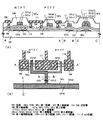
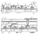
なお、断面構造は図1(A)に示し、上面図は図1(B)に示す。また、図1(A)、(B)は同一の符号を用いて説明する。また、図1(B)のA−A’、B−B’、C−C’で切った時の断面図は図1(A)においてA−A’、B−B’、C−C’で示した各断面図に対応する。
【0025】
まず、図1(A)において、101は基板、102a、102b、102cは第1配線、103は第1絶縁層、104はNTFTの活性層、105はPTFTの活性層、106は第2絶縁層である。
【0026】
その上には第1導電層107a1、第2導電層107a2を積層してなる第2配線107a、同様に第1導電層107b1、第2導電層107b2を積層してなる第2配線107b、第1導電層107c1、第2導電層107c2を積層してなる第2配線107c、第1導電層107d1、第2導電層107d2で第3導電層d3を挟んだ構造からなる第2配線107dを有する。
【0027】
また、108は第1層間絶縁層、109〜111は第3配線であり、109、110がソース配線(ソース電極を含む)、111がドレイン配線(ドレイン電極を含む)である。
【0028】
以上のような構造でなるCMOS回路において、基板101としてはガラス基板、石英基板、金属基板、ステンレス基板、プラスチック基板、セラミックス基板またはシリコン基板を用いることができる。シリコン基板を用いる場合は予めに表面を酸化して酸化珪素膜を設けておくと良い。
【0029】
また、第1配線は図1(B)に示すように同一パターンからなる配線であるが、説明の便宜上、部分ごとに102a、102b、102cに区別した。ここでは第1配線102aは活性層103との交差部、第1配線102bはTFT間の接続部、第1配線102cは各回路に共通の電源供給部を指し示している。
【0030】
この時、第1配線102aはNTFTのサブゲート電極として機能する。即ち、チャネル形成領域112の電荷制御は第1配線102aと、第1配線102aと同電位である第2配線(メインゲート電極)107aとで行われ、第1配線102aのみがLDD領域113にゲート電圧(または所定の電圧)を印加することができるような構造となっている。
【0031】
従って、第2配線107aのみをゲート電極として機能させた場合はGOLD構造にならない(LDD構造となる)が、第1配線102aと組み合わせることで初めてGOLD構造を実現することができる。この構造の利点は後述するとして、さらに、この第1配線102aは遮光層としての機能をも兼ねている。
【0032】
なお、第1配線の材料としては導電性を有していればどのような材料を用いても構わない。ただし、後のプロセス温度に耐えうる耐熱性を有する材料であることが望ましい。例えばタンタル(Ta)、チタン(Ti)、タングステン(W)、モリブデン(Mo)、またはシリコン(Si)から選ばれた元素を主成分(成分比が50%以上)とする導電膜、或いは前記元素を組み合わせた合金膜やシリサイド膜を用いても構わない。
【0033】
また、本実施形態の特徴としては、第1配線102aがNTFTのみに設けられ、PTFTには設けられない点が挙げられる。図1(A)の場合、PTFTはオフセット領域もLDD領域も形成されていないが、どちらか一方または両方を備えていても構わない。
【0034】
このような構造であるため、図1(B)に示すように第1配線は電源供給部から接続部を経由してNTFTに至り、NTFTのサブゲート電極として機能することになる。
【0035】
また、第2配線も全て同一パターンからなる配線であるが、説明の便宜上、部分ごとに区別した。区別の仕方は第1配線とほぼ同様であり、図1(A)において、107aがNTFTの活性層104との交差部、107bがPTFTの活性層105との交差部、107cがTFT間の接続部、107dが電源供給部である。
【0036】
第2配線は基本的に二種類の導電層を積層して形成する。上層及び下層のどちらの導電層も導電性を有していればよく、タンタル(Ta)膜、チタン(Ti)膜、タングステン(W)膜、モリブデン(Mo)膜、シリコン(Si)膜を自由に組み合わせて形成することができる。また、これらの合金膜やシリサイド膜を用いても構わない。
【0037】
但し、積層した後で同一形状にパターニングが可能な材料を選択する必要がある。即ち、積層した後で一括にエッチングできるか、上層側をマスクにして下層側がエッチングできるような組み合わせが望ましい。また、下層に設ける導電層は第3導電層107d3とのエッチング選択比が確保されなければならない。
【0038】
第3導電層107d3はアルミニウム(Al)または銅(Cu)を主成分(成分比が50%以上をいう)とする導電層であり、第1導電層107d1、第2導電層107d2で包み込んだ構造(以下、クラッド構造という)とすることで第2配線107dを形成している。この第2配線107dは電源供給部に相当する配線を形成する。
【0039】
CMOS回路はAM−LCDのドライバー回路やその他の信号処理回路として多用されるインバータ回路である。これらのドライバー回路や信号処理回路は高密度に集積化されているため、配線幅を極力細くすることが望まれる。従って、活性層との交差部(ゲート電極部)や接続部(配線の引き回し部)はなるべく細くするように設計する。また、これらの部分は配線自体の長さもさほど長くないので、配線抵抗の影響を受けにくい。
【0040】
しかしながら、電源供給部は配線自体の長さが長いため、配線抵抗の影響を大きく受けてしまう。そのため、本実施形態では抵抗の低いアルミニウムや銅を主成分とする材料を用い、配線抵抗を軽減している。また、第2配線107dのような構造とすると多少配線幅が太くなってしまうが、電源供給部は複雑に集積化された回路の外に形成されるため問題とはならない。
【0041】
なお、対角4インチ以下のAM−LCDのように、全体的に回路が小さく極端に長い配線がないような半導体装置に本願発明を用いる場合、電源供給部となる配線も短いため、必ずしも上述のクラッド構造を用いなくても良い。換言すれば、図1に示した構造は対角4インチ以上のAM−LCDに対して有効であるとも言える。
【0042】
以上のように、本実施形態のCMOS回路の特徴としては以下の二つが上げられる。
1.NTFTのみに第1配線(サブゲート配線)が設けられ、第1配線に第2配線(メインゲート配線)と同じ電圧を印加するか、所定の電圧を印加することでNTFTをGOLD構造とすることができる。
2.第2配線のゲート電極部や接続部は配線幅を細くして高集積化し、電源供給部は第1及び第2導電層で低抵抗な第3導電層を挟み込む構造(クラッド構造)とすることで低抵抗化することができる。
【0043】
[実施形態2]
本願発明の実施の形態について、NTFTを画素TFTとして用いた画素マトリクス回路を例にとって説明する。なお、この画素マトリクス回路は「実施形態1」で説明したCMOS回路と同一の基板上に同時に形成されるため、同一名称の配線に関する詳細は「実施形態1」の記載を参考にすれば良い。
【0044】
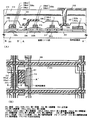
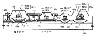
なお、断面構造は図2(A)に示し、上面図は図2(B)に示す。また、図2(A)、(B)は同一の符号を用いて説明する。また、図2(B)のA−A’、B−B’で切った時の断面図は図2(A)においてA−A’、B−B’で示した各断面図に対応する。
【0045】
まず、図2(A)において、201は基板、202a、202b、202cは第1配線、203は第1絶縁層、204は画素TFT(NTFT)の活性層、205は第2絶縁層である。なお、画素TFTはダブルゲート構造を例示しているが、シングルゲート構造でも良いし、三つ以上のTFTを直列に接続したマルチゲート構造としても構わない。
【0046】
第2絶縁層203の上には第1導電層206a1、第2導電層206a2で第3導電層206a3を挟んだ構造からなる第2配線206a、第1導電層206b1、第2導電層206b2を積層してなる第2配線206b、第1導電層206c1、第2導電層206c2を積層してなる第2配線206c、第1導電層207a、第2導電層207bを積層してなる容量配線207を有する。
【0047】
この時、容量配線207は第1絶縁層205を誘電体として、活性層204(具体的にはドレイン領域から延在する領域)との間に保持容量を形成する。この際、第1絶縁層205を窒化珪素膜の上に酸化珪素膜を設けた積層構造としておき、保持容量となる部分の酸化珪素膜を選択的に除去した後で第2配線を形成すれば比誘電率の高い窒化珪素膜のみを誘電体とする保持容量を実現できる。
【0048】
また、208は第1層間絶縁層、209、210は第3配線であり、209がソース配線(ソース電極を含む)、210がドレイン配線(ドレイン電極を含む)である。さらに、その上には第2層間絶縁層211、ブラックマスク212、第3層間絶縁層213、画素電極214が設けられる。
【0049】
また、第1配線は図2(B)に示すように同一パターンからなる配線であるが、説明の便宜上、部分ごとに202a、202b、202cに区別した。ここでは第1配線202aはゲート電極として機能しない配線部、202b、202cは活性層204との交差部であり、ゲート電極部として機能する部分である。
【0050】
なお、ここに示した第1配線は「実施形態1」で説明した第1配線と同時に形成される。従って、材料等の説明は省略する。
【0051】
この時、第1配線202b、202cは画素TFTの遮光膜として機能する。即ち、「実施形態1」で説明したようなサブゲート配線としての機能はなく、固定電位にしておくか、フローティング状態(電気的に孤立した状態)にしておく。固定電位としては、接地電位かソース電源電位(ソース配線と同電位)にしておけば良い。そうすることでホットキャリア注入によって発生したホールをチャネル形成領域から引き抜くことが可能となり、その結果、電荷の中和がなされてホットキャリアが消滅する。
【0052】
このようにチャネル形成領域215、216の電荷制御は第1配線206bと第1配線206cとで行われ、LDD構造として動作する。これによりオフ電流の増加を効果的に抑制することができる。
【0053】
このように本実施形態に示した画素マトリクス回路では画素TFTとしてNTFTが用いられ、その構造は「実施形態1」で説明したCMOS回路のNTFTと同一構造である。しかしながら、CMOS回路では第1配線に所定電圧を印加してサブゲート配線として用いることでGOLD構造を実現したのに対し、画素マトリクス回路では第1配線を固定電位またはフローティング電位にしてLDD構造として用いる点に違いがある。
【0054】
即ち、本願発明の最大の特徴は、同一基板上に同一構造のNTFTを形成しておき、第1配線(サブゲート配線)に印加する電圧の有無によってGOLD構造とLDD構造とを使い分ける点にある。これにより工程数を増やすことなく、最適な回路設計が可能となるのである。
【0055】
また、第2配線206a、206b、206cは、206b、206cがゲート電極部であり、206aが配線部である。配線部はできるだけ配線抵抗を低くすることが望ましいのでクラッド構造を採用している。しかし、ゲート電極部の方は配線幅がチャネル長を決定するため、第1導電層と第2導電層との積層として線幅を細くするような設計としている。
【0056】
なお、クラッド構造の内容や効果については「実施形態1」で既に説明したのでここでの説明は省略する。また、「実施形態1」でも説明したように、対角4インチ以下のAM−LCDには必ずしもクラッド構造とする必要がないことは言うまでもない。
【0057】
以上に示した本願発明の構成について、以下に示す実施例でさらに詳細に説明する。
【0058】
【実施例】
[実施例1]
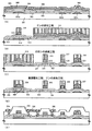
本実施例では、「実施形態1」で説明したCMOS回路の作製方法について説明する。説明には図3を用いる。
【0059】
まず、基板301としてガラス基板を用意し、その上に第1配線302a、302b、302cを形成した。第1配線の材料としては、スパッタ法によりタングステンシリサイド(WSix)膜、シリコン膜を順次積層した積層膜を用いた。勿論、積層順序が逆であっても良いし、成膜手段としてCVD法を用いることも可能である。また、上記積層膜を形成した後、表面に酸化膜が形成されていると表面保護という意味で有効であった。
【0060】
勿論、第1配線302a、302b、302cは導電性を有する膜であれば良いので、他の金属膜や合金膜等を用いても構わない。なお、テーパー角の小さいパターン形成が可能なクロム膜やタンタル膜を用いると平坦性を向上させることができるため有効である。
【0061】
次に、珪素(シリコン)を含む絶縁膜でなる第1絶縁層303を形成した。第1絶縁層303は活性層を保護する下地膜としての役割を果たすと同時に、第1配線302aをサブゲート配線として用いる際のゲート絶縁膜として機能する。
【0062】
本実施例ではまず50nmの窒化珪素膜を成膜し、その上に80nmの酸化珪素膜を積層した構造を採用した。他にもSiOxNy(x/y=0.01〜100)で示される酸化窒化珪素膜(窒化酸化珪素膜ともいう)を用いても良い。その際、窒素の含有量を酸素の含有量よりも多くすることで耐圧を向上させることが可能である。
【0063】
次に、50nm厚の非晶質珪素膜(図示せず)を形成し、公知のレーザー結晶化技術により結晶化して結晶質珪素膜を形成した。そして結晶質珪素膜をパターニングして活性層304、305を形成した。本実施例では、結晶化工程を、パルス発振型のKrFエキシマレーザー光を線状に集光して非晶質珪素膜に照射することによって行った。
【0064】
尚、本実施例では活性層に用いる半導体膜として非晶質珪素膜を結晶化した結晶質珪素膜を用いたが、他の半導体膜として微結晶珪素膜を用いても構わないし、直接結晶質珪素膜を成膜しても良い。また、珪素膜以外に、シリコンゲルマニウム膜等の化合物半導体膜を用いることも可能である。
【0065】
次に、活性層304、305を覆って、酸化珪素膜、酸化窒化珪素膜、窒化珪素膜またはそれらの積層膜でなる第2絶縁層306を形成した。ここではプラズマCVD法で酸化窒化珪素膜を100nmの厚さに形成した。この第2絶縁層は第2配線をメインゲート配線として用いる際のゲート絶縁膜として機能する。
【0066】
次に、第1導電層として20nm厚のタンタル膜307を形成し、その上にスカンジウムを添加したアルミニウム膜でなる第3導電層308を形成した。さらに、200nm厚のタンタル膜でなる第2導電層309を形成した。これらの成膜方法はスパッタ法でもCVD法でも良い。
【0067】
こうして図3(A)の状態が得られたら、レジストマスク310、311を形成し、第1導電層307と第2導電層309とをエッチングした。こうしてタンタル膜の積層構造でなる第2配線312が形成された。この第2配線312は図1(A)の第2配線(メインゲート配線)107aに相当する。
【0068】
次に、15族に属する元素(代表的にはリンまたは砒素)を添加し、低濃度不純物領域313を形成した。また、このとき同時にNTFTのチャネル形成領域314が画定した。本実施例では15族に属する元素としてリンを用い、質量分離を行わないイオンドーピング法を用いて添加した。(図3(B))
【0069】
添加条件としては、加速電圧を90keVとし、1×10¹⁶〜1×10¹⁹atoms/cm3(好ましくは5×1017〜5×1018atoms/cm3)の濃度でリンが添加されるようにドーズ量を調節した。この濃度が後にLDD領域の不純物濃度になるので精密に制御する必要がある。
【0070】
次に、レジストマスク310、311を除去し、新たにレジストマスク315〜318を形成した。そして第1導電層307と第2導電層309をエッチングして第2配線319〜321を形成した。この第2配線319、320、321はそれぞれ順に図1(A)の第2配線107b、107c、107dに相当する。
【0071】
次に、13族に属する元素(代表的にはボロンまたはガリウム)を添加し、不純物領域322を形成した。また、このとき同時にPTFTのチャネル形成領域323が画定した。本実施例では13族に属する元素としてボロンを用い、質量分離を行わないイオンドーピング法を用いて添加した。(図3(C))
【0072】
添加条件としては、加速電圧を75keVとし、1×10¹⁹〜5×10²¹atoms/cm3(好ましくは1×1020〜1×1021atoms/cm3)の濃度でボロンが添加されるようにドーズ量を調節した。
【0073】
次に、レジストマスク315〜318を除去した後、再びレジストマスク324〜327を形成した。本実施例では、これらのレジストマスクは裏面露光法を用いて形成した。即ち、レジストマスク324、326、327は第1配線がマスクとなり、レジストマスク325は第2配線がマスクとなっている。第1配線をマスクとなる場合は少し光の回り込みがあるので、第1配線よりも線幅が細くなる。この線幅は露光条件によって制御することが可能である。
【0074】
勿論、これらのレジストマスクを、マスクを用いて形成することもできる。その場合、パターン設計の自由度は高くなるがマスク枚数が増えてしまう。
【0075】
こうしてレジストマスク324〜327が形成されたら、15族に属する元素(本実施例ではリン)の添加工程を行った。ここでは加速電圧を90keVとし、1×10¹⁹〜5×10²¹atoms/cm3(好ましくは1×1020〜1×1021atoms/cm3)の濃度でリンが添加されるようにドーズ量を調節した。
【0076】
この工程によりNTFTのソース領域328、ドレイン領域329およびLDD領域330が画定した。また、PTFTのソース領域331、ドレイン領域332が画定した。この工程ではPTFTのソース領域とドレイン領域にもリンが添加されるが、前工程でさらに高い濃度のボロンが添加されていれば、N型に反転しないためP型を維持したままとなる。
【0077】
こうしてNTFTおよびPTFTに一導電性を付与する不純物元素を添加したら、ファーネスアニール法、レーザーアニール法、ランプアニール法またはそれらの手法を併用して不純物元素の活性化を行った。
【0078】
こうして図3(D)の状態が得られたら、酸化珪素膜、窒化珪素膜、酸化窒化珪素膜、樹脂膜またはそれらの積層膜でなる第1層間絶縁層333を形成した。そしてコンタクトホールを開けてソース配線334、335、ドレイン配線336を形成した。(図3(E))
【0079】
本実施例では第1層間絶縁層333として、最初に窒化珪素膜を50nm形成し、さらに酸化珪素膜を950nm形成した2層構造とした。また、本実施例ではソース配線およびドレイン配線を、チタン膜100nm、チタンを含むアルミニウム膜300nm、チタン膜150nmをスパッタ法で連続して形成した3層構造の積層膜をパターニングして形成した。
【0080】
こうして図3(E)に示すような構造のCMOS回路が完成した。本実施例のCMOS回路は図1(A)に示した構造であり、それについての説明は「実施形態1」で詳細に説明したのでここでの説明は省略する。また、図1(A)の構造を得るにあたって、本実施例の作製工程に限定される必要はない。例えば、NTFTをダブルゲート構造とし、PTFTをシングルゲート構造とするようなことも可能である。
【0081】
なお、本実施例で説明したCMOS回路はAM−LCDにおいてはドライバー(駆動)回路(シフトレジスタ回路、バッファ回路、レベルシフタ回路、サンプリング回路など)やその他の信号処理回路(分割回路、D/Aコンバータ回路、γ補正回路、オペアンプ回路など)を構成する基本単位回路である。
【0082】
本実施例ではNTFTの第1配線をサブゲート配線として用いることで実質的なGOLD構造を実現することができ、ホットキャリア注入による劣化を防ぐことができる。従って、非常に信頼性の高い回路を形成することができる。
【0083】
また、集積度の高い場所では配線の線幅を細くし、集積度のあまり高くない場所(電源供給部)ではクラッド構造とすることで配線抵抗を減らし、配線抵抗による遅延時間を低減する構造となっている。
【0084】
〔実施例2〕
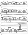
本実施例では「実施形態2」で説明した画素マトリクス回路の作製方法について説明する。説明には図4、図5を用いる。なお、画素マトリクス回路は同一基板上において、実施例1に示したCMOS回路と同時に形成されるため、実施例1の作製工程に対応させて説明する。従って、必要に応じて図3と同じ符号を使って説明することとする。
【0085】
まず、ガラス基板301上に第2配線401a、401b、401cを形成した。これら第2配線の材料は実施例1で説明した通りである。次に、実施例1を参考にして第1絶縁層303、画素TFTの活性層402、第2絶縁層306、第1導電層307、第3導電層403、第2導電層309を形成した。こうして図4(A)の状態が得られた、この時、同時形成されているCMOS回路は図3(A)の状態にある。
【0086】
次に、レジストマスク404〜407を形成し、第1導電層307と第2導電層309のエッチングを行った。こうして第2配線408、409および容量配線410が形成された。なお、第2配線408は図2(A)の第2配線206bに、第2配線409は図2(A)の第2配線206cに相当する。また、容量配線410は図2(A)の容量配線207に相当する。
【0087】
次に、後にLDD領域を形成するためのリンの添加工程を行い、低濃度不純物領域411〜413を形成した。また、この時、チャネル形成領域414、415が画定した。この工程は図3(B)の工程に対応する。従って、図4(B)の工程において、第2配線の材料や膜厚、およびリンの添加条件は実施例1と同様である。
【0088】
次に、図3(C)に相当する工程を行った。まず、レジストマスク416、417を形成し、第1導電層307と第2導電層309のエッチングを行うことにより第2配線418を形成した。この第2配線418は図2(A)の第2配線206aに相当する。
【0089】
次に、CMOS回路のPTFTを作製するためにボロンの添加工程を行った。本実施例の場合、画素TFTはNTFTで形成されるため、画素マトリクス回路はレジストマスク417で全面的に覆った状態とした。(図4(C))
【0090】
次に、レジストマスク416、417を除去した後、裏面露光法によりレジストマスク419〜422を形成した。そして、リンの添加工程を行い、ソース領域423、ドレイン領域424、LDD領域425を形成した。この時、裏面露光条件やリンの添加条件等は実施例1の図3(D)の工程に従えば良い。
【0091】
なお、図4(D)では説明の便宜上、ソース領域やドレイン領域と記載したが、画素TFTの場合は画素への充電時と放電時とでソース領域とドレイン領域が逆転するので明確な区別はない。
【0092】
こうしてリンおよびボロンの添加工程が終了したら、実施例1と同様に不純物元素の活性化工程を行った。そして、第1層間絶縁層333を形成し、コンタクトホールを形成してソース配線426、ドレイン配線427を形成した。こうして図4(E)の状態を得た。この時、CMOS回路は図3(E)の状態となっている。
【0093】
次に、ソース配線426およびドレイン配線427を覆って第2層間絶縁層428を形成した。本実施例ではパッシベーション膜として30nm厚の窒化珪素膜を形成し、その上に700nm厚のアクリル膜を形成した。勿論、酸化珪素膜など珪素を主成分とする絶縁膜を用いても良いし、他の樹脂膜を用いても良い。他の樹脂膜としては、ポリイミド膜、ポリアミド膜、BCB(ベンゾシクロブテン)膜などを使用することができる。
【0094】
次に、100nm厚のチタン膜でなるブラックマスク429を形成した。ブラックマスク427は遮光性を有する膜であれば他の膜を用いても良い。代表的にはクロム膜、アルミニウム膜、タンタル膜、タングステン膜、モリブデン膜、チタン膜またはそれらの積層膜を用いれば良い。
【0095】
次に第3層間絶縁層430を形成した。本実施例では1μm厚のアクリル膜としたが、第2層間絶縁層と同様の材料を用いることができる。
【0096】
次に、第3層間絶縁層430にコンタクトホールを形成し、透明導電膜(代表的にはITO膜)でなる画素電極431を形成した。この時、画素電極431はドレイン配線427と電気的に接続される。従って、コンタクトホールは非常に深いものとなるので、内側の側壁がテーパー形状または曲面を有するように形成すると画素電極が断線するなどの不良を防ぐのに有効であった。
【0097】
こうして図5(A)に示すような構造の画素マトリクス回路が完成した。なお、本実施例では画素電極として透明導電膜を用いて透過型AM−LCDを作製する例を示したが、画素電極として反射率の高い金属膜(アルミニウムを主成分とする金属膜など)を用いることで容易に反射型AM−LCDを作製することが可能である。
【0098】
また、図5(A)の状態となった基板をアクティブマトリクス基板という。本実施例では、実際にAM−LCDを作製した場合の構造も併せて説明する。
【0099】
図5(A)の状態が得られたら、配向膜432を80nmの厚さに形成した。次に、対向基板を作製した。対向基板はガラス基板433上にカラーフィルタ434、透明電極(対向電極)435、配向膜436を形成したものを準備した。そして、それぞれの配向膜432、435に対してラビング処理を行い、シール材(封止材)を用いてアクティブマトリクス基板と対向基板とを貼り合わせた。そして、その間に液晶436を保持させた。なお、セルギャップを維持するためのスペーサは必要に応じて設ければ良い。
【0100】
こうして図5(B)に示す構造のAM−LCD(画素マトリクス回路の部分)が完成した。本実施例に示した第2層間絶縁層428と第3層間絶縁層430は実際には実施例1に示したCMOS回路上にも形成されることになる。また、ブラックマスク429や画素電極431を形成すると同時に、それらを構成する材料で配線を形成し、その配線をAM−LCDのドライバー回路や信号処理回路の引き回し配線(第4配線または第5配線)として用いることも可能である。
【0101】
本実施例の場合、画素TFTに設けられた第1配線401b、401cは固定電位(接地電位またはソース電位)に設定した。こうしておくことで、ホットキャリア注入によってドレイン端部に生じたホール(正孔)を第1配線に引き抜くことができるため、信頼性の向上に適した構造となる。勿論、第1配線401b、401cをフローティング状態にしておくこともできるが、その場合にはホールの引き抜き効果を期待できない。
【0102】
また、図2(B)の上面図にも示したように、配線部に位置する第2配線418はクラッド構造を採用し、配線抵抗を極力減らすような構造とした。
【0103】
〔実施例3〕
本実施例では本願発明の画素マトリクス回路やCMOS回路(具体的にはCMOS回路で形成されたドライバー回路や信号処理回路)を具備したAM−LCDの外観を図6に示す。
【0104】
アクティブマトリクス基板601には画素マトリクス回路602、信号線駆動回路(ソースドライバー回路)603、走査線駆動回路(ゲートドライバー回路)604、信号処理回路(信号分割回路、D/Aコンバータ回路、γ補正回路等)605が形成され、FPC(フレキシブルプリントサーキット)606が取り付けられている。なお、607は対向基板である。
【0105】
ここでアクティブマトリクス基板601上に形成された各種回路をさらに詳しく図示したブロック図を図7に示す。
【0106】
図7において、701は画素マトリクス回路であり、画像表示部として機能する。また、702aはシフトレジスタ回路、702bはレベルシフタ回路、702cはバッファ回路である。これらでなる回路が全体としてゲートドライバー回路を形成している。
【0107】
なお、図7に示したAM−LCDのブロック図ではゲートドライバー回路を、画素マトリクス回路を挟んで設け、それぞれで同一ゲート配線を共有している、即ち、どちらか片方のゲートドライバーに不良が発生してもゲート配線に電圧を印加することができるという冗長性を持たせている。
【0108】
また、703aはシフトレジスタ回路、703bはレベルシフタ回路、703cはバッファ回路、703dはサンプリング回路であり、これらでなる回路が全体としてソースドライバー回路を形成している。画素マトリクス回路を挟んでソースドライバー回路と反対側にはプリチャージ回路14が設けられている。
【0109】
本願発明を用いることで図6に示したような回路を有するAM−LCDの信頼性を大幅に向上させることができる。その際、ドライバー回路や信号処理回路を形成するCMOS回路は実施例1に従えばよく、画素マトリクス回路は実施例2に従えば良い。
【0110】
〔実施例4〕
本実施例では、「実施形態1」に示したCMOS回路や「実施形態2」に示した画素マトリクス回路の構造を異なるものとした場合について説明する。具体的には、回路の要求する仕様に応じて構造を異ならせる例を示す。
【0111】
なお、CMOS回路の基本構造は図1(A)に示した構造、画素マトリクス回路の基本構造は図2(A)に示した構造であるため、本実施例では必要箇所のみに符号を付して説明することとする。
【0112】
まず、図8(A)に示した構造はNTFTのソース側のLDD領域をなくし、ドレイン側のみにLDD領域801を設けた構造である。ドライバー回路や信号処理回路に用いられるCMOS回路は高速動作を要求されるため、動作速度を低下させる要因となりうる抵抗成分は極力排除する必要がある。
【0113】
本願発明のCMOS回路の場合、サブゲート配線として機能する第1配線にゲート電圧を印加することによってGOLD構造を実現し、ホットキャリア注入による劣化を防いでいる。しかしながら、ホットキャリア注入が生じるのはチャネル形成領域のドレイン領域側の端部であり、その部分にゲート電極とオーバーラップした(重なった)LDD領域が存在すれば良い。
【0114】
従って、必ずしもチャネル形成領域のソース領域側の端部にはLDD領域を設けておく必要はなく、却ってソース領域側に設けられたLDD領域が抵抗成分として働いてしまう恐れがある。そのため、図8(A)のような構造とすることは動作速度を改善する上で有効である。
【0115】
なお、図8(A)の構造はソース領域とドレイン領域とが入れ替わる画素TFTのような動作をする場合には適用できない。CMOS回路の場合、通常はソース領域およびドレイン領域が固定されるため、図8(A)のような構造を実現することができる。
【0116】
次に、図8(B)は基本的には図8(A)と同様であるが、LDD領域802の幅が図8(A)よりも狭く形成されている。具体的には0.05〜0.5μm(好ましくは0.1〜0.3μm)とする。図8(B)の構造はソース領域側の抵抗成分をなくすだけでなく、ドレイン領域側の抵抗成分を極力減らすような構造となっている。
【0117】
このような構造は実際にはシフトレジスタ回路のように3〜5Vといった低電圧で駆動し、高速動作を要求するような回路に適している。動作電圧が低いのでLDD領域(厳密にはゲート電極にオーバーラップしたLDD領域)が狭くなってもホットキャリア注入の問題は顕在化しない。
【0118】
勿論、場合によってはシフトレジスタ回路のみNTFTのLDD領域を完全になくすようなこともできる。その場合、同じドライバー回路内でも、シフトレジスタ回路のNTFTにはLDD領域がなく、他の回路には図1(A)や図8(B)に示した構造を採用するようなこともできる。
【0119】
次に、図8(C)はNTFTをダブルゲート構造、PTFTをシングルゲート構造としたCMOS回路の例である。この場合、チャネル形成領域803、804のドレイン領域に近い側のみの端部にLDD領域805、806を設ける。
【0120】
図3(D)に示したようにLDD領域の幅は裏面露光工程における光の回り込み量で決定するが、マスク合わせによってレジストマスクを形成すれば自由にマスク設計を行うことができる。図8(C)に示した構造においてもマスクを用いれば片側のみにLDD領域を設けることは容易である。
【0121】
しかし、本実施例のようにゲート配線(第2配線)807a、807bと第1配線808、809とをずらして形成することで、裏面露光法を用いても片側のみにLDD領域を形成することが可能となる。
【0122】
このような構造とすることでソース領域側のLDD領域による抵抗成分をなくし、ダブルゲート構造とすることでソース−ドレイン間にかかる電界を分散させて緩和する効果がある。
【0123】
次に、図8(D)の構造は画素マトリクス回路の一実施形態である。図8(D)の構造の場合、ソース領域またはドレイン領域に近い片側のみにLDD領域809、810を設ける。即ち、二つのチャネル形成領域811と812の間にはLDD領域を設けない構造とする。
【0124】
画素TFTの場合、充電と放電を繰り返す動作を行うためソース領域とドレイン領域とが頻繁に入れ替わることになる。従って、図8(D)の構造とすることでどちらがドレイン領域となってもチャネル形成領域のドレイン領域側にLDD領域を設けた構造となる。逆に、チャネル形成領域811と812の間の領域は電界集中がないので抵抗成分となるLDD領域をなくした方がオン電流(TFTがオン状態にある時に流れる電流)を大きくするには有効である。
【0125】
なお、図8(A)〜(D)の構造において、ソース領域側のチャネル形成領域の端部にはLDD領域を設けない構造としているが、幅の狭いものであれば設けられていても構わない。そのような構造はマスク合わせによってレジストマスクを形成しても良いし、第1配線と第2配線の位置を調節した上で裏面露光法を用いて形成しても良い。
【0126】
なお、本実施例の構成は実施例1、2と組み合わせられることは言うまでもなく、実施例3に示したAM−LCDに用いても良い。
【0127】
〔実施例5〕
本実施例では実施例2に示した画素マトリクス回路とは異なる構造の保持容量を形成した場合について説明する。説明には図9を用いる。なお、基本的な構造は図2(A)に示したものと同じであるので、本実施例では必要箇所のみに符号を付して説明することとする。
【0128】
まず、図9(A)に示した構造は保持容量を第1配線と同一層に形成された容量配線901、第1絶縁層902および活性層(厳密にはドレイン領域から延在する部分)903とで形成する。
【0129】
この構造の利点は、活性層のうち保持容量の電極として機能する部分にも高濃度に13族または15族に属する元素が添加され、導電型を有している点である。勿論、13族または15族に属する元素はソース領域またはドレイン領域の形成工程と同時に形成すれば良い。
【0130】
「実施形態2」で説明した構造の場合、保持容量の電極として機能する活性層は第2配線がマスクとなるため導電型を付与する不純物元素が添加されず、容量配線に常に電圧を印加して活性層に反転層が形成された状態を維持しなければらない。しかしながら、図9(A)の構造では、保持容量の電極として機能する活性層自身が導電性を有しているため、電圧を印加する必要がなく、接地電位などに固定しておけば良いだけである。
【0131】
このように余分な電圧を印加する必要がない分、消費電力を抑えるのに有効な構造であると言える。
【0132】
また、図9(B)の構造は、図2(A)に示した保持容量の構造と図9(A)に示した保持容量の構造とを組み合わせた例である。具体的には、第1配線と同一層の第1容量配線904、第1絶縁層905および活性層906で第1保持容量を形成し、活性層906、第2絶縁層907および第2配線と同一層の第2容量配線908で第2保持容量を形成する。
【0133】
この構造では工程数をなんら増やすことなく、図2(A)や図9(A)に示した保持容量の構造の2倍近い容量を確保することが可能である。特に、AM−LCDが高精細になれば開口率を稼ぐために、保持容量の面積を小さくすることが必要となる。そのような場合に図9(B)の構造は有効である。
【0134】
なお、本実施例の構造を実施例3に示したAM−LCDに対して用いることは有効である。
【0135】
〔実施例6〕
本実施例では図1(A)に示したCMOS回路や図2(A)に示した画素マトリクス回路において、第2配線を構成する第1導電層を省略した場合の例を図10に示す。なお、図10(A)において図1(A)または図2(A)と同じ構成の部分には同一の符号を付している。
【0136】
図10(A)のCMOS回路は、第2配線11〜13が全て単層のタンタル膜で形成されている。即ち、図1(A)の構造と比較すると第1導電層を省略し、第2導電層のみで第2配線を形成した構成となる。なお、膜厚は200〜400nmとすれば良い。勿論、タンタル以外に、チタン、タングステン、モリブデン、またはシリコンから選ばれた元素を主成分とする導電膜、或いは前記元素を組み合わせた合金膜やシリサイド膜を用いても良い。
【0137】
このような構造とした場合、第2配線の電源供給部(図1(A)でクラッド構造となっていた部分)は第3導電層14aを第2導電層14bで覆った構造となる。ただし、この構造では第3導電層14aの構成元素であるアルミニウムや銅が第2絶縁層106中に拡散する恐れがある。そのため、第2絶縁層106の表面に窒化珪素膜を設けておくと、アルミニウムや銅の拡散を効果的に防止することが可能である。
【0138】
また、本実施例の構造は画素マトリクス回路に対しても適用できる。図10(B)の画素マトリクス回路は、第2配線(ゲート配線)16、17および容量配線が第2導電層(本実施例ではタンタル膜)のみでなり、ゲート配線の中でも配線抵抗を抑えたい部分には、第3導電層15aを第2導電層15bで覆った構造を採用している。
【0139】
勿論、図10(A)、図10(B)に示した回路はどちらも同一基板上に同時形成されることは言うまでもない。
【0140】
また、本実施例の構造は実施例1および実施例2に示した作製工程において、第1導電層の形成工程を省略するのみで実現できる。また、実施例3のAM−LCDに適用することもできるし、実施例4、5に示した構成と組み合わせることも可能である。
【0141】
〔実施例7〕
本実施例では図1(A)に示したCMOS回路や図2(A)に示した画素マトリクス回路において、NTFTのゲート電極部をクラッド構造とする場合の例を図11に示す。なお、図11(A)において図1(A)または図2(A)と同じ構成の部分には同一の符号を付している。
【0142】
図11(A)に示したCMOS回路では、NTFTのゲート電極21が第1導電層21aと第2導電層21bとで第3導電層21cを包み込んだクラッド構造となっている。この時、チャネル形成領域22の長さは第3導電層21cの線幅に一致する。
【0143】
また、LDD領域23は実質的に二つの領域に区別することができる。一方は第2配線の一部であるゲート電極21と重なっており、他方はゲート電極21と重なっていない。即ち、本実施例の構造では、第2配線の一部であるゲート電極のみでGOLD構造を実現することができる。、さらにゲート電極にオーバーラップしたLDD領域の外側に、ゲート電極にオーバーラップしないLDD領域が設けられるため、非常にオフ電流を小さくすることができる。
【0144】
図11(B)に示した画素マトリクス回路の場合も同様であり、画素TFTのゲート電極24、25はどちらも第1導電層24a、25aと第2導電層24b、25bとで第3導電層24c、25cを包み込んだクラッド構造となっている。この時、チャネル形成領域26、27の長さは第3導電層24c、25cの線幅に一致する。また、LDD領域28、29はどちらもLDD領域23と同様に実質的に二つの領域に区別できる。
【0145】
「実施形態1」や「実施形態2」に示した構造の場合、CMOS回路では第1配線(サブゲート配線)にゲート電圧を印加することでGOLD構造が実現されるが、画素マトリクス回路ではオフ電流を下げるためにLDD構造となるようにしている。これはGOLD構造の欠点であるオフ電流の増加を避けるためであり、そのためオン電流の劣化を抑制するというGOLD構造そのものの利点は得られない。
【0146】
しかしながら、本実施例の構造では画素マトリクス回路であってもGOLD構造のNTFTが実現されるため、さらに信頼性を高めることができる。勿論、画素TFTをGOLD構造にできる理由は、ゲート電極にオーバーラップするLDD領域の外側に、ゲート電極にオーバーラップしないLDD領域を設けたからに他ならない。
【0147】
ここで、本実施例の構造を実現するための作製工程について図12を用いて説明する。ただし、基本的には実施例1で説明した工程と同一であるので、必要箇所のみに新たに符号を付して説明する。
【0148】
まず、実施例1の工程に従って第3導電層308を形成した。本実施例の場合、第3導電層308の形成と同時にNTFTの上にも第3導電層31を形成した。そして、レジストマスク32を形成し、リンの添加工程を行った。この添加条件は実施例1の図3(B)の工程を参考にすれば良い。この工程により低濃度不純物領域33、34が形成され、チャネル形成領域35が画定した。(図12(A))
【0149】
次に、レジストマスク32を除去した後、第2導電層36、37を形成した。この工程のよりNTFTのメインゲート配線38が形成された。(図12(B))
【0150】
次に、レジストマスク315〜318を形成し、ボロンの添加工程を行った。添加条件は実施例1の図3(C)の工程を参考にすれば良い。こうしてリンおよびボロンの添加工程が終了したら、実施例1と同様の手段で添加した不純物元素の活性化を行い、図12(C)の状態が得られた。
【0151】
次に、レジストマスク315〜318を除去した後、裏面露光法により再びレジストマスク324〜327を形成し、リンの添加工程を行った。添加条件は実施例1の図3(D)の工程を参考にすれば良い。
【0152】
この工程によりNTFTのソース領域39、ドレイン領域40および低濃度不純物領域(LDD領域)41が形成された。(図12(D))
【0153】
この時、LDD領域41は、ゲート電極38とオーバーラップしている部分の長さが0.1〜3.5μm(代表的には0.1〜0.5μm、好ましくは0.1〜0.3μm)となるようにし、ゲート電極38とオーバーラップしていない部分の長さが0.5〜3.5μm(代表的には1.5〜2.5μm)となるようにすれば良い。
【0154】
この後は実施例1と同様の工程を経て、第1層間絶縁膜108、ソース配線109、110、ドレイン配線111を形成することで図11(A)に示すような構造のCMOS回路が完成した。
【0155】
なお、本実施例ではCMOS回路の作製工程を例にとって説明したが、画素マトリクス回路においてもほぼ同様の作製工程で図11(B)の構造が得られる。従って、ここでの説明は省略する。
【0156】
また、本実施例の構造は実施例3のAM−LCDに適用することもできるし、実施例4〜6に示した構成とも自由に組み合わせることが可能である。
【0157】
〔実施例8〕
実施例1の図3(D)の工程において、裏面露光法でレジストマスク324〜327を形成した後、第2絶縁層306をエッチングして除去し、露呈した活性層にリンを添加することは有効である。
【0158】
こうすることによりリンを添加する際の加速電圧を10keV程度にまで下げることができ、ドーピング装置の負担を減らすことができる。また、スループットを大幅に向上させることができる。この事は実施例2の図4(D)に示した工程においても同様である。
【0159】
なお、本実施例の構成は実施例3のAM−LCDに適用することもできるし、実施例4〜7に示した構成とも自由に組み合わせることが可能である。
【0160】
〔実施例9〕
本実施例ではドライバー回路に用いるCMOS回路において、NTFTのオフ電流を低減するための構造について図13を用いて説明する。
【0161】
図13において、NTFTのLDD領域51は、実質的に第1配線102aにオーバーラップしている部分としていない部分とに区別できる。従って、第1配線102aにゲート電圧が印加された際、図13のNTFTはゲート電極にオーバーラップしたLDD領域の外側に、ゲート電極にオーバーラップしていないLDD領域を有する構造となる。
【0162】
このような構造は実施例8でも説明したように、GOLD構造の利点であるオン電流の劣化を防ぐ効果を有し、且つ、GOLD構造の欠点であるオフ電流の増加を抑制した電気特性を得ることができる。従って、非常に優れた信頼性を有するCMOS回路を実現することが可能である。
【0163】
また、ここではCMOS回路の場合を例にとって説明したが、本実施例の構造を画素マトリクス回路に適用しても構わない。
【0164】
また、本実施例の構造を実現するためには、実施例1の図3(D)に示した工程において裏面露光法を用いなければ良い。即ち、通常のマスク合わせにより第1配線よりも幅の広いレジストマスクを設け、その後、リンの添加工程を行えば本実施例の構造を容易に得ることができる。
【0165】
なお、LDD領域の長さ(ゲート電極にオーバーラップしている部分としていない部分の長さ)は実施例8に示した範囲を参考にすれば良い。
【0166】
なお、本実施例の構成は実施例3のAM−LCDに適用することもできるし、実施例4〜7に示した構成とも自由に組み合わせることが可能である。
【0167】
〔実施例10〕
本実施例では、実施例1または実施例2に示した活性層を形成するにあたってレーザー結晶化以外の手段を用いた場合について説明する。
【0168】
具体的には、活性層として用いる結晶質半導体膜を、触媒元素を用いた熱結晶化法により形成する例を示す。触媒元素を用いる場合、特開平7−130652号公報(米国出願番号08/329,644または米国出願番号08/430,623に対応)、特開平8−78329号公報で開示された技術を用いることが望ましい。特に触媒元素としてはニッケルが好適である。
【0169】
なお、本実施例の構成は実施例1乃至実施例9の全ての構成と自由に組み合わせることが可能である。
【0170】
〔実施例11〕
本実施例は活性層を形成する方法として、実施例10に示した熱結晶化法を用い、そこで用いた触媒元素を結晶質半導体膜から除去する工程を行った例を示す。本実施例ではその方法として、特開平10−135468号公報(米国出願番号08/951,193に対応)または特開平10−135469号公報(米国出願番号08/951,819に対応)に記載された技術を用いる。
【0171】
同公報に記載された技術は、非晶質半導体膜の結晶化に用いた触媒元素を結晶化後にハロゲンのゲッタリング作用を用いて除去する技術である。同技術を用いることで、結晶質半導体膜中の触媒元素の濃度を1×10¹⁷atoms/cm3以下、好ましくは1×1016atoms/cm3にまで低減することができる。
【0172】
なお、本実施例の構成は実施例1乃至実施例10の全ての構成と自由に組み合わせることが可能である。
【0173】
〔実施例12〕
本実施例は活性層を形成する方法として、実施例10に示した熱結晶化法を用い、そこで用いた触媒元素を結晶質半導体膜から除去する工程を行った例を示す。本実施例ではその方法として、特開平10−270363号公報(米国出願番号09/050,182に対応)に記載された技術を用いる。
【0174】
同公報に記載された技術は、非晶質半導体膜の結晶化に用いた触媒元素を結晶化後にリンのゲッタリング作用を用いて除去する技術である。同技術を用いることで、結晶質半導体膜中の触媒元素の濃度を1×10¹⁷atoms/cm3以下、好ましくは1×1016atoms/cm3にまで低減することができる。
【0175】
なお、本実施例の構成は実施例1乃至実施例10の全ての構成と自由に組み合わせることが可能である。
【0176】
〔実施例13〕
本実施例では、実施例12で示したリンによるゲッタリング工程の別形態について説明する。なお、基本的な工程は図1に従うものであるので、相違点のみに着目して説明する。
【0177】
まず、実施例1の工程に従って図3(D)の状態を得た。図14(A)は図3(D)の状態からレジストマスク324〜327を除去した状態を表している。ただし、TFTの活性層となる半導体層の形成には実施例10に示した熱結晶化技術を用いている。
【0178】
この時、NTFTのソース領域328及びドレイン領域329、並びにPTFTのソース領域331及びドレイン領域332には1×10¹⁹〜1×10²¹atoms/cm3(好ましくは5×1020atoms/cm3)の濃度でリンが含まれている。
【0179】
本実施例ではこの状態で、窒素雰囲気中で500〜800℃、1〜24時間、例えば600℃、12時間の加熱処理の工程を行う。この工程により、添加されたn型及びp型を付与する不純物元素を活性化することができた。さらに、結晶化工程の後残存していた触媒元素(本実施例ではニッケル)が矢印の方向に移動し、前述のソース領域及びドレイン領域に含まれたリンの作用によって同領域にゲッタリング(捕獲)することができた。その結果、チャネル形成領域からニッケルを1×10¹⁷atoms/cm3以下にまで低減することができた。
【0180】
図14(B)の工程が終了したら、以降の工程は実施例1の工程に従えば、図3(E)に示すようなCMOS回路を作製することができる。勿論、同様のことが画素マトリクス回路でも行われることは言うまでもない。
【0181】
なお、本実施例の構成は実施例1乃至実施例10の全ての構成と自由に組み合わせることが可能である。
【0182】
〔実施例14〕
本願発明のTFT構造はAM−LCDのような電気光学装置だけでなく、あらゆる半導体回路に適用することが可能である。即ち、RISCプロセッサ、ASICプロセッサ等のマイクロプロセッサに適用しても良いし、D/Aコンバータ等の信号処理回路から携帯機器(携帯電話、PHS、モバイルコンピュータ)用の高周波回路に適用しても良い。
【0183】
さらに、従来のMOSFET上に層間絶縁膜を形成し、その上に本願発明を用いて半導体回路を作製したような三次元構造の半導体装置を実現することも可能である。このように本願発明は現在LSIが用いられている全ての半導体装置に適用することが可能である。即ち、SIMOX、Smart−Cut(SOITEC社の登録商標)、ELTRAN(キャノン株式会社の登録商標)などのSOI構造(単結晶半導体薄膜を用いたTFT構造)に本願発明を適用しても良い。
【0184】
また、本実施例の半導体回路は実施例1、2、4〜13のどのような組み合わせからなる構成を用いても実現することができる。
【0185】
〔実施例15〕
本願発明を実施して形成されたCMOS回路や画素マトリクス回路は様々な電気光学装置や半導体回路に適用することができる。即ち、それら電気光学装置や半導体回路を部品として組み込んだ電子機器全てに本願発明を実施できる。
【0186】
その様な電子機器としては、ビデオカメラ、デジタルカメラ、プロジェクター、プロジェクションTV、ヘッドマウントディスプレイ(ゴーグル型ディスプレイ)、カーナビゲーション、パーソナルコンピュータ、携帯情報端末(モバイルコンピュータ、携帯電話または電子書籍等)などが挙げられる。それらの一例を図15に示す。
【0187】
図15(A)は携帯電話であり、本体2001、音声出力部2002、音声入力部2003、表示装置2004、操作スイッチ2005、アンテナ2006で構成される。本願発明を音声出力部2002、音声入力部2003、表示装置2004やその他の信号制御回路に適用することができる。
【0188】
図15(B)はビデオカメラであり、本体2101、表示装置2102、音声入力部2103、操作スイッチ2104、バッテリー2105、受像部2106で構成される。本願発明を表示装置2102、音声入力部2103やその他の信号制御回路に適用することができる。
【0189】
図15(C)はモバイルコンピュータ(モービルコンピュータ)であり、本体2201、カメラ部2202、受像部2203、操作スイッチ2204、表示装置2205で構成される。本願発明は表示装置2205やその他の信号制御回路に適用できる。
【0190】
図15(D)はゴーグル型ディスプレイであり、本体2301、表示装置2302、アーム部2303で構成される。本発明は表示装置2302やその他の信号制御回路に適用することができる。
【0191】
図15(E)はリア型プロジェクターであり、本体2401、光源2402、表示装置2403、偏光ビームスプリッタ2404、リフレクター2405、2406、スクリーン2407で構成される。本発明は表示装置2403やその他の信号制御回路に適用することができる。
【0192】
図15(F)はフロント型プロジェクターであり、本体2501、光源2502、表示装置2503、光学系2504、スクリーン2505で構成される。本発明は表示装置2502やその他の信号制御回路に適用することができる。
【0193】
以上の様に、本願発明の適用範囲は極めて広く、あらゆる分野の電子機器に適用することが可能である。また、本実施例の電子機器は実施例1〜14のどのような組み合わせからなる構成を用いても実現することができる。
【0194】
【発明の効果】
本願発明は同一構造のNTFTを、活性層の下側に設けた第1配線の電圧を制御することでGOLD構造として用いたり、LDD構造として用いたりする点に特徴がある。即ち、工程数を増やしたり煩雑にすることなく、同一基板上にGOLD構造とLDD構造とを実現することができる。
【0195】
そのため、AM−LCDやAM−LCDを表示ディスプレイとして有する電子機器等の半導体装置において、回路が要求する仕様に応じて適切な性能の回路を配置することが可能となり、半導体装置の性能や信頼性を大幅に向上させることができた。
【図面の簡単な説明】
【図1】 CMOS回路の構造を示す図。
【図2】 画素マトリクス回路の構造を示す図。
【図3】 CMOS回路の作製工程を示す図。
【図4】 画素マトリクス回路の作製工程を示す図。
【図5】 画素マトリクス回路の作製工程を示す図。
【図6】 AM−LCDの外観を示す図。
【図7】 AM−LCDのブロック構成を示す図。
【図8】 CMOS回路または画素マトリクス回路の構造を示す図。
【図9】 画素マトリクス回路(特に保持容量)の構造を示す図。
【図10】 CMOS回路または画素マトリクス回路の構造を示す図。
【図11】 CMOS回路または画素マトリクス回路の構造を示す図。
【図12】 CMOS回路の作製工程を示す図。
【図13】 CMOS回路の構造を示す図。
【図14】 CMOS回路の作製工程を示す図。
【図15】 電子機器の一例を示す図。[0001]
BACKGROUND OF THE INVENTION
The present invention relates to a semiconductor device having a circuit composed of thin film transistors (hereinafter referred to as TFTs). For example, the present invention relates to an electro-optical device typified by a liquid crystal display panel and a configuration of an electronic apparatus in which such an electro-optical device is mounted as a component.
[0002]
Note that in this specification, a semiconductor device refers to all devices that can function by utilizing semiconductor characteristics, and an electro-optical device, a semiconductor circuit, and an electronic device are also semiconductor devices.
[0003]
[Prior art]
Since a thin film transistor (hereinafter referred to as TFT) can be formed on a transparent glass substrate, application development to an active matrix liquid crystal display (hereinafter referred to as AM-LCD) has been actively promoted. Since a TFT using a crystalline semiconductor film (typically a polysilicon film) has high mobility, a high-definition image display can be realized by integrating functional circuits on the same substrate. Yes.
[0004]
An active matrix type liquid crystal display device requires 1 million TFTs with only pixels as the screen resolution becomes higher. When a functional circuit is further added, a larger number of TFTs are required, and in order to stably operate the liquid crystal display device, it is necessary to ensure the reliability of individual TFTs and to operate them stably.
[0005]
However, TFTs are not necessarily equivalent to MOSFETs manufactured on a single crystal semiconductor substrate in terms of reliability. As in the case of MOSFETs, when TFTs are operated for a long period of time, a phenomenon such as a decrease in mobility and on-current occurs. One of the causes of such a phenomenon is deterioration of characteristics due to hot carriers generated with an increase in channel electric field.
[0006]
On the other hand, in a MOSFET, an LDD (Lightly Doped Drain) structure is well known as a technique for improving reliability. In this structure, a low concentration impurity region is provided inside the source / drain region, and this low concentration impurity region is called an LDD region. This structure is also adopted in the TFT.
[0007]
Further, in MOSFETs, a structure is known in which an LDD region overlaps (overlaps) with a gate electrode to some extent via a gate insulating film. There are several methods for forming this structure. For example, structures called GOLD (Gate-drain Overlapped LDD) and LATID (Large-tilt-angle implanted drain) are known. With such a structure, hot carrier resistance could be increased.
[0008]
Attempts have also been made to apply such MOSFET structures to TFTs. However, in the case of a GOLD structure (in this specification, a structure having an LDD region to which a gate voltage is applied is referred to as a GOLD structure. Conversely, a structure having only an LDD region to which a gate voltage is not applied is referred to as an LDD structure). There is a problem that off current (current that flows when the TFT is in an off state) becomes large as compared with the LDD structure. Therefore, it is not suitable for use in a circuit that wants to suppress the off current as much as possible, such as a pixel matrix circuit of an AM-LCD.
[0009]
[Problems to be solved by the invention]
An object of the present invention is to provide an AM-LCD having high reliability by forming each circuit of the AM-LCD with a TFT having an appropriate structure according to the function. Accordingly, it is an object to improve the reliability of a semiconductor device (electronic device) having such an AM-LCD.
[0010]
[Means for Solving the Problems]
The configuration of the invention disclosed in this specification is as follows.
In a semiconductor device including a CMOS circuit formed of an N-channel TFT and a P-channel TFT,
The CMOS circuit has a structure in which only the N-channel TFT has an active layer sandwiched between a first wiring and a second wiring through an insulating layer,
The active layer includes a low concentration impurity region in contact with the channel formation region,
The low concentration impurity region is formed so as to overlap the first wiring and not to overlap the second wiring.
[0011]
In the above configuration, the first wiring and the second wiring may be electrically connected. That is, the first wiring and the second wiring have the same potential, and the same voltage can be applied (applied) to the active layer.
[0012]
In addition, the configuration of other inventions is as follows:
In a semiconductor device including a CMOS circuit formed of an N-channel TFT and a P-channel TFT,
The CMOS circuit has a structure in which only the N-channel TFT has an active layer sandwiched between a first wiring and a second wiring through an insulating layer,
The second wiring includes a portion having a laminated structure of a first conductive layer and a second conductive layer, and a portion having a structure in which a third conductive layer is enclosed by the first conductive layer and the second conductive layer. It is characterized by having.
[0013]
In the above configuration, the third conductive layer uses a material having a lower resistance value than the first conductive layer or the second conductive layer. Specifically, the first conductive layer or the second conductive layer mainly contains an element selected from tantalum (Ta), titanium (Ti), tungsten (W), molybdenum (Mo), or silicon (Si). It is preferable to use a conductive film as a component, or an alloy film or a silicide film in which the above elements are combined. The third conductive layer is preferably a film containing aluminum or copper as a main component.
[0014]
In addition, the configuration of other inventions is as follows:
In a semiconductor device including a pixel matrix circuit having a pixel TFT formed of an N-channel TFT and a storage capacitor,
The pixel TFT has a structure in which an active layer is sandwiched between a first wiring and a second wiring through an insulating layer,
The active layer includes a low concentration impurity region in contact with the channel formation region,
The low concentration impurity region is formed so as to overlap the first wiring and not to overlap the second wiring.
[0015]
Note that in the above structure, the first wiring may be held at a ground potential or a source power supply potential, or may be held at a floating potential.
[0016]
In addition, the configuration of other inventions is as follows:
In a semiconductor device including a pixel matrix circuit having a pixel TFT formed of an N-channel TFT,
The pixel TFT has a structure in which an active layer is sandwiched between a first wiring and a second wiring through an insulating layer,
The second wiring includes a portion having a laminated structure of a first conductive layer and a second conductive layer, and a portion having a structure in which a third conductive layer is enclosed by the first conductive layer and the second conductive layer. It is characterized by having.
[0017]
In addition, the configuration of other inventions is as follows:
In a semiconductor device having a pixel matrix circuit and a driver circuit formed on the same substrate,
The pixel TFT included in the pixel matrix circuit and the N-channel TFT included in the driver circuit have a structure in which an active layer is sandwiched between a first wiring and a second wiring through an insulating layer,
The first wiring connected to the pixel TFT is held at a fixed potential or a floating potential, and the first wiring connected to the N-channel TFT included in the driver circuit is connected to the N-channel TFT included in the driver circuit. It is characterized by being held at the same potential as the connected second wiring.
[0018]
In the above structure, the active layer includes a low-concentration impurity region in contact with the channel formation region,
The low concentration impurity region is formed so as to overlap the first wiring and not the second wiring.
[0019]
In addition, the second wiring includes a portion having a laminated structure of a first conductive layer and a second conductive layer, and a portion having a structure in which the third conductive layer is enclosed by the first conductive layer and the second conductive layer. And have.
[0020]
In addition, the configuration of other inventions is as follows:
In a method for manufacturing a semiconductor device including a CMOS circuit formed of an N-channel TFT and a P-channel TFT,
Forming a first wiring on a substrate;
Forming a first insulating layer on the first wiring;
Forming an active layer on the first insulating layer as an active layer of the N-channel TFT and an active layer of the P-channel TFT;
Forming a second insulating layer covering the active layer of the N-channel TFT and the active layer of the P-channel TFT;
Forming a second wiring on the second insulating layer,
The first wiring is formed so as to cross only an active layer of the N-channel TFT.
[0021]
In the above configuration, the second wiring has a structure in which a third conductive layer is enclosed by a portion having a laminated structure of a first conductive layer and a second conductive layer, and the first conductive layer and the second conductive layer. The part which becomes is formed.
[0022]
In addition, the configuration of other inventions is as follows:
In a method for manufacturing a semiconductor device including a CMOS circuit formed of an N-channel TFT and a P-channel TFT,
Forming a first wiring on a substrate;
Forming a first insulating layer on the first wiring;
Forming an active layer on the first insulating layer as an active layer of the N-channel TFT and an active layer of the P-channel TFT;
Forming a second insulating layer covering the active layer of the N-channel TFT and the active layer of the P-channel TFT;
Forming a first conductive layer on the second insulating layer;
Forming a patterned third conductive layer on the first conductive layer;
Forming a second conductive layer covering the third conductive layer,
The first wiring is formed so as to cross only an active layer of the N-channel TFT.
[0023]
DETAILED DESCRIPTION OF THE INVENTION
[Embodiment 1]
An embodiment of the present invention will be described by taking as an example a CMOS circuit (inverter circuit) in which an N-channel TFT (hereinafter referred to as NTFT) and a P-channel TFT (hereinafter referred to as PTFT) are combined.
[0024]
The cross-sectional structure is shown in FIG. 1A, and the top view is shown in FIG. 1A and 1B will be described using the same reference numerals. 1B is a cross-sectional view taken along the lines AA ′, BB ′, and CC ′ in FIG. 1B. The cross-sectional views taken along the lines AA ′, BB ′, and CC ′ in FIG. Corresponds to each of the cross-sectional views shown in FIG.
[0025]
First, in FIG. 1A, 101 is a substrate, 102a, 102b and 102c are first wirings, 103 is a first insulating layer, 104 is an NTFT active layer, 105 is a PTFT active layer, and 106 is a second insulating layer. It is.
[0026]
On top of this, the
[0027]
[0028]
In the CMOS circuit having the above structure, the
[0029]
Further, the first wiring is a wiring having the same pattern as shown in FIG. 1B, but for convenience of description, the first wiring is divided into 102a, 102b, and 102c. Here, the
[0030]
At this time, the
[0031]
Therefore, when only the
[0032]
In addition, as long as it has electroconductivity as a material of 1st wiring, you may use what kind of material. However, it is desirable that the material has heat resistance that can withstand the subsequent process temperature. For example, a conductive film whose main component is an element selected from tantalum (Ta), titanium (Ti), tungsten (W), molybdenum (Mo), or silicon (Si), or the element Alternatively, an alloy film or a silicide film may be used.
[0033]
As a feature of the present embodiment, the
[0034]
Due to such a structure, as shown in FIG. 1B, the first wiring reaches the NTFT from the power supply portion through the connection portion, and functions as a sub-gate electrode of the NTFT.
[0035]
The second wirings are all wirings having the same pattern, but are distinguished for each part for convenience of explanation. The method of distinction is almost the same as that of the first wiring. In FIG. 1A, 107a is an intersection with the NTFT
[0036]
The second wiring is basically formed by laminating two kinds of conductive layers. It is sufficient that both the upper and lower conductive layers have conductivity, and a tantalum (Ta) film, a titanium (Ti) film, a tungsten (W) film, a molybdenum (Mo) film, and a silicon (Si) film can be freely used. Can be formed in combination. Further, these alloy films and silicide films may be used.
[0037]
However, it is necessary to select a material that can be patterned into the same shape after lamination. That is, it is desirable to be able to etch in a lump after stacking or a combination in which the lower layer side can be etched using the upper layer side as a mask. In addition, the conductive layer provided in the lower layer must have an etching selectivity with respect to the third conductive layer 107d3.
[0038]
The third conductive layer 107d3 is a conductive layer containing aluminum (Al) or copper (Cu) as a main component (having a component ratio of 50% or more), and has a structure in which the first conductive layer 107d1 and the second conductive layer 107d2 are enclosed. The second wiring 107d is formed by adopting (hereinafter referred to as a cladding structure). The second wiring 107d forms a wiring corresponding to the power supply unit.
[0039]
The CMOS circuit is an inverter circuit frequently used as a driver circuit for AM-LCD and other signal processing circuits. Since these driver circuits and signal processing circuits are integrated with high density, it is desired to make the wiring width as thin as possible. Therefore, the crossing portion (gate electrode portion) and connection portion (wiring routing portion) with the active layer are designed to be as thin as possible. In addition, since the length of the wiring itself is not so long, these portions are not easily affected by the wiring resistance.
[0040]
However, the power supply unit is greatly affected by the wiring resistance because the length of the wiring itself is long. Therefore, in this embodiment, a material mainly composed of aluminum or copper having a low resistance is used to reduce the wiring resistance. Further, if the structure is the second wiring 107d, the wiring width is somewhat thick, but the power supply unit is not a problem because it is formed outside the circuit integrated in a complicated manner.
[0041]
Note that when the present invention is used for a semiconductor device in which the circuit is small and there is no extremely long wiring, such as an AM-LCD having a diagonal size of 4 inches or less, the wiring serving as a power supply unit is also short, so that it is not necessarily described above. The clad structure may not be used. In other words, it can be said that the structure shown in FIG. 1 is effective for an AM-LCD having a diagonal of 4 inches or more.
[0042]
As described above, there are the following two features of the CMOS circuit of this embodiment.
1. Only the NTFT is provided with a first wiring (sub-gate wiring), and the same voltage as that of the second wiring (main gate wiring) is applied to the first wiring, or the NTFT has a GOLD structure by applying a predetermined voltage. it can.
2. The gate electrode part and the connection part of the second wiring are made highly integrated by narrowing the wiring width, and the power supply part has a structure (cladding structure) in which the low-resistance third conductive layer is sandwiched between the first and second conductive layers. The resistance can be lowered.
[0043]
[Embodiment 2]
An embodiment of the present invention will be described by taking a pixel matrix circuit using NTFTs as pixel TFTs as an example. Since the pixel matrix circuit is formed on the same substrate as the CMOS circuit described in the “Embodiment 1” at the same time, the description of “Embodiment 1” may be referred to for details regarding the wiring having the same name.
[0044]
The cross-sectional structure is shown in FIG. 2A, and the top view is shown in FIG. 2A and 2B will be described using the same reference numerals. 2B is a cross-sectional view taken along lines AA ′ and BB ′ in FIG. 2B, which corresponds to the cross-sectional views indicated by AA ′ and BB ′ in FIG.
[0045]
2A, 201 is a substrate, 202a, 202b, and 202c are first wirings, 203 is a first insulating layer, 204 is an active layer of a pixel TFT (NTFT), and 205 is a second insulating layer. In addition, although the pixel TFT has illustrated the double gate structure, it may be a single gate structure or a multi-gate structure in which three or more TFTs are connected in series.
[0046]
On the second insulating
[0047]
At this time, the
[0048]
[0049]
Further, the first wiring is a wiring having the same pattern as shown in FIG. 2B, but for the sake of convenience of explanation, the first wiring is divided into 202a, 202b, and 202c. Here, the
[0050]
The first wiring shown here is formed at the same time as the first wiring described in the first embodiment. Therefore, description of materials etc. is omitted.
[0051]
At this time, the
[0052]
As described above, charge control of the
[0053]
As described above, in the pixel matrix circuit shown in this embodiment, NTFT is used as the pixel TFT, and its structure is the same as that of the TFT of the CMOS circuit described in “Embodiment 1.” However, in the CMOS circuit, a GOLD structure is realized by applying a predetermined voltage to the first wiring and using it as a sub-gate wiring, whereas in the pixel matrix circuit, the first wiring is used as an LDD structure with a fixed potential or a floating potential. There is a difference.
[0054]
That is, the greatest feature of the present invention is that NTFTs having the same structure are formed on the same substrate, and the GOLD structure and the LDD structure are selectively used depending on the presence or absence of a voltage applied to the first wiring (sub-gate wiring). This makes it possible to design an optimum circuit without increasing the number of processes.
[0055]
In the
[0056]
The contents and effects of the clad structure have already been described in “Embodiment 1”, and a description thereof will be omitted here. Further, as described in “Embodiment 1,” it goes without saying that an AM-LCD having a diagonal of 4 inches or less does not necessarily have a clad structure.
[0057]
The configuration of the present invention described above will be described in more detail in the following examples.
[0058]
【Example】
[Example 1]
In this example, a method for manufacturing the CMOS circuit described in Embodiment Mode 1 will be described. FIG. 3 is used for the description.
[0059]
First, a glass substrate was prepared as the
[0060]
Of course, the
[0061]
Next, a first insulating
[0062]
In this embodiment, a structure in which a 50 nm silicon nitride film is first formed and an 80 nm silicon oxide film is laminated thereon is employed. In addition, a silicon oxynitride film (also referred to as a silicon nitride oxide film) represented by SiOxNy (x / y = 0.01 to 100) may be used. At that time, the breakdown voltage can be improved by making the nitrogen content higher than the oxygen content.
[0063]
Next, an amorphous silicon film (not shown) having a thickness of 50 nm was formed and crystallized by a known laser crystallization technique to form a crystalline silicon film. Then, the crystalline silicon film was patterned to form
[0064]
In this embodiment, a crystalline silicon film obtained by crystallizing an amorphous silicon film is used as the semiconductor film used for the active layer. However, a microcrystalline silicon film may be used as another semiconductor film, and the crystalline film is directly crystalline. A silicon film may be formed. In addition to the silicon film, a compound semiconductor film such as a silicon germanium film can be used.
[0065]
Next, a second insulating
[0066]
Next, a
[0067]
When the state of FIG. 3A is thus obtained, resist
[0068]
Next, an element belonging to Group 15 (typically phosphorus or arsenic) was added to form a low
[0069]
As addition conditions, the acceleration voltage is 90 keV and 1 × 10 16 ~ 1x10 19 atoms / cm Three (Preferably 5 × 10 17 ~ 5x10 18 atoms / cm Three The dose was adjusted so that phosphorus was added at a concentration of. Since this concentration later becomes the impurity concentration of the LDD region, it needs to be precisely controlled.
[0070]
Next, the resist
[0071]
Next, an element belonging to group 13 (typically boron or gallium) was added to form an
[0072]
As an addition condition, the acceleration voltage is set to 75 keV and 1 × 10 19 ~ 5x10 twenty one atoms / cm Three (Preferably 1 × 10 20 ~ 1x10 twenty one atoms / cm Three The dose was adjusted so that boron was added at a concentration of.
[0073]
Next, after removing the resist
[0074]
Of course, these resist masks can also be formed using a mask. In this case, the degree of freedom in pattern design increases, but the number of masks increases.
[0075]
When the resist
[0076]
This step defined the
[0077]
After adding the impurity element imparting one conductivity to the NTFT and PTFT in this way, the impurity element was activated by using furnace annealing, laser annealing, lamp annealing, or a combination thereof.
[0078]
When the state of FIG. 3D is obtained in this way, a first
[0079]
In this embodiment, the first
[0080]
Thus, a CMOS circuit having a structure as shown in FIG. The CMOS circuit of this example has the structure shown in FIG. 1A, and the description thereof has been described in detail in “Embodiment 1”, and thus description thereof is omitted here. Further, in obtaining the structure of FIG. 1A, it is not necessary to be limited to the manufacturing process of this embodiment. For example, the NTFT may have a double gate structure and the PTFT may have a single gate structure.
[0081]
Note that the CMOS circuit described in this embodiment is a driver circuit (shift register circuit, buffer circuit, level shifter circuit, sampling circuit, etc.) and other signal processing circuits (dividing circuit, D / A converter) in the AM-LCD. Circuit, γ correction circuit, operational amplifier circuit, etc.).
[0082]
In this embodiment, a substantial GOLD structure can be realized by using the first wiring of the NTFT as the sub-gate wiring, and deterioration due to hot carrier injection can be prevented. Therefore, a highly reliable circuit can be formed.
[0083]
In addition, the line width of the wiring is narrowed in places where the degree of integration is high, and in places where the degree of integration is not very high (power supply part), a cladding structure is used to reduce the wiring resistance and reduce the delay time due to the wiring resistance. It has become.
[0084]
[Example 2]
In this example, a method for manufacturing the pixel matrix circuit described in Embodiment Mode 2 is described. 4 and 5 are used for the description. Since the pixel matrix circuit is formed on the same substrate at the same time as the CMOS circuit shown in the first embodiment, the description will be made in accordance with the manufacturing process of the first embodiment. Therefore, description will be made using the same reference numerals as in FIG. 3 as necessary.
[0085]
First,
[0086]
Next, resist
[0087]
Next, phosphorus was added to form an LDD region later, so that low-
[0088]
Next, a step corresponding to FIG. First, resist
[0089]
Next, a boron addition process was performed in order to produce a PTFT of a CMOS circuit. In this embodiment, since the pixel TFT is formed of NTFT, the pixel matrix circuit is entirely covered with the resist
[0090]
Next, after removing the resist
[0091]
Note that in FIG. 4D, for convenience of description, the source region and the drain region are described. However, in the case of a pixel TFT, the source region and the drain region are reversed between when the pixel is charged and when the pixel is discharged. Absent.
[0092]
When the phosphorus and boron addition steps were completed in this manner, the impurity element activation step was performed in the same manner as in Example 1. Then, a first
[0093]
Next, a second
[0094]
Next, a
[0095]
Next, a third
[0096]
Next, a contact hole was formed in the third
[0097]
Thus, a pixel matrix circuit having a structure as shown in FIG. 5A was completed. Note that although an example in which a transmissive AM-LCD is manufactured using a transparent conductive film as a pixel electrode is shown in this embodiment, a highly reflective metal film (such as a metal film containing aluminum as a main component) is used as a pixel electrode. By using it, it is possible to easily produce a reflective AM-LCD.
[0098]
The substrate in the state of FIG. 5A is referred to as an active matrix substrate. In this embodiment, a structure when an AM-LCD is actually manufactured is also described.
[0099]
When the state of FIG. 5A was obtained, the
[0100]
Thus, an AM-LCD (pixel matrix circuit portion) having the structure shown in FIG. 5B was completed. The second
[0101]
In this embodiment, the
[0102]
Further, as shown in the top view of FIG. 2B, the
[0103]
Example 3
In this embodiment, an appearance of an AM-LCD including a pixel matrix circuit and a CMOS circuit (specifically, a driver circuit and a signal processing circuit formed of a CMOS circuit) of the present invention is shown in FIG.
[0104]
The
[0105]
FIG. 7 is a block diagram showing in more detail various circuits formed on the
[0106]
In FIG. 7,
[0107]
In the block diagram of the AM-LCD shown in FIG. 7, the gate driver circuit is provided across the pixel matrix circuit, and each of them shares the same gate wiring, that is, one of the gate drivers is defective. Even so, redundancy is provided such that a voltage can be applied to the gate wiring.
[0108]
[0109]
By using the present invention, the reliability of an AM-LCD having a circuit as shown in FIG. 6 can be greatly improved. At that time, the CMOS circuit for forming the driver circuit and the signal processing circuit may be according to the first embodiment, and the pixel matrix circuit may be according to the second embodiment.
[0110]
Example 4
In this example, a case where the CMOS circuit shown in “Embodiment 1” and the pixel matrix circuit shown in “Embodiment 2” are different in structure will be described. Specifically, an example in which the structure is changed according to the specifications required by the circuit is shown.
[0111]
Since the basic structure of the CMOS circuit is the structure shown in FIG. 1A and the basic structure of the pixel matrix circuit is the structure shown in FIG. 2A, only necessary portions are denoted by reference numerals in this embodiment. Will be explained.
[0112]
First, the structure shown in FIG. 8A is a structure in which the
[0113]
In the case of the CMOS circuit of the present invention, a GOLD structure is realized by applying a gate voltage to the first wiring functioning as a sub-gate wiring, thereby preventing deterioration due to hot carrier injection. However, hot carrier injection occurs at the end of the channel formation region on the drain region side, and an LDD region that overlaps (overlaps with) the gate electrode only has to exist there.
[0114]
Therefore, it is not always necessary to provide an LDD region at the end of the channel formation region on the source region side, and the LDD region provided on the source region side may work as a resistance component. Therefore, the structure as shown in FIG. 8A is effective in improving the operation speed.
[0115]
Note that the structure of FIG. 8A cannot be applied to the case of operation like a pixel TFT in which a source region and a drain region are interchanged. In the case of a CMOS circuit, since the source region and the drain region are usually fixed, a structure as shown in FIG. 8A can be realized.
[0116]
Next, FIG. 8B is basically the same as FIG. 8A, but the width of the
[0117]
Such a structure is actually suitable for a circuit that is driven at a low voltage of 3 to 5 V and requires high-speed operation, such as a shift register circuit. Since the operating voltage is low, the problem of hot carrier injection does not become apparent even if the LDD region (strictly, the LDD region overlapping with the gate electrode) becomes narrow.
[0118]
Of course, in some cases, only the shift register circuit can completely eliminate the LDD region of the NTFT. In that case, even in the same driver circuit, the NTFT of the shift register circuit does not have an LDD region, and the structure shown in FIGS. 1A and 8B can be adopted for other circuits.
[0119]
Next, FIG. 8C shows an example of a CMOS circuit in which the NTFT has a double gate structure and the PTFT has a single gate structure. In this case,
[0120]
As shown in FIG. 3D, the width of the LDD region is determined by the amount of light sneaking in the back surface exposure process. However, if a resist mask is formed by mask alignment, the mask design can be freely performed. Even in the structure shown in FIG. 8C, it is easy to provide an LDD region only on one side if a mask is used.
[0121]
However, by forming the gate wirings (second wirings) 807a and 807b and the
[0122]
With such a structure, the resistance component due to the LDD region on the source region side is eliminated, and the double gate structure has an effect of dispersing and relaxing the electric field applied between the source and the drain.
[0123]
Next, the structure of FIG. 8D is an embodiment of a pixel matrix circuit. In the case of the structure in FIG. 8D,
[0124]
In the case of the pixel TFT, the source region and the drain region are frequently switched because an operation of repeating charging and discharging is performed. Therefore, the structure shown in FIG. 8D has a structure in which an LDD region is provided on the drain region side of the channel formation region, regardless of which is the drain region. Conversely, since the region between the
[0125]
8A to 8D, the LDD region is not provided at the end of the channel formation region on the source region side, but may be provided as long as the width is narrow. Absent. In such a structure, a resist mask may be formed by mask alignment, or the back surface exposure method may be used after adjusting the positions of the first wiring and the second wiring.
[0126]
Needless to say, the configuration of this embodiment can be combined with the first and second embodiments, and may be used for the AM-LCD shown in the third embodiment.
[0127]
Example 5
In this embodiment, a case where a storage capacitor having a structure different from that of the pixel matrix circuit shown in Embodiment 2 is formed will be described. FIG. 9 is used for the description. Since the basic structure is the same as that shown in FIG. 2A, in this embodiment, only necessary portions will be described with reference numerals.
[0128]
First, the structure shown in FIG. 9A has a
[0129]
The advantage of this structure is that an element belonging to Group 13 or 15 is added at a high concentration to the portion of the active layer that functions as the electrode of the storage capacitor, and has a conductivity type. Of course, the elements belonging to
[0130]
In the case of the structure described in “Embodiment 2,” the active layer functioning as an electrode of the storage capacitor serves as a mask for the second wiring, so that no impurity element imparting conductivity is added, and a voltage is always applied to the capacitor wiring. Thus, the state where the inversion layer is formed in the active layer must be maintained. However, in the structure of FIG. 9A, since the active layer itself that functions as an electrode of the storage capacitor has conductivity, it is not necessary to apply a voltage, and it is only necessary to fix it to a ground potential or the like. It is.
[0131]
Thus, it can be said that the structure is effective in suppressing power consumption because it is not necessary to apply an extra voltage.
[0132]
9B is an example in which the structure of the storage capacitor illustrated in FIG. 2A and the structure of the storage capacitor illustrated in FIG. 9A are combined. Specifically, a first storage capacitor is formed by the
[0133]
With this structure, it is possible to secure a capacity nearly twice that of the structure of the storage capacity shown in FIGS. 2A and 9A without increasing the number of steps. In particular, if the AM-LCD has a high definition, it is necessary to reduce the area of the storage capacitor in order to increase the aperture ratio. In such a case, the structure of FIG. 9B is effective.
[0134]
Note that it is effective to use the structure of this embodiment for the AM-LCD shown in Embodiment 3.
[0135]
Example 6
In this embodiment, an example in which the first conductive layer constituting the second wiring is omitted in the CMOS circuit shown in FIG. 1A and the pixel matrix circuit shown in FIG. 2A is shown in FIG. Note that in FIG. 10A, parts having the same configuration as in FIG. 1A or 2A are denoted with the same reference numerals.
[0136]
In the CMOS circuit of FIG. 10A, the
[0137]
In such a structure, the power supply portion of the second wiring (the portion having the cladding structure in FIG. 1A) has a structure in which the third conductive layer 14a is covered with the second conductive layer 14b. However, in this structure, aluminum or copper, which are constituent elements of the third conductive layer 14a, may diffuse into the second insulating
[0138]
The structure of this embodiment can also be applied to a pixel matrix circuit. In the pixel matrix circuit of FIG. 10B, the second wiring (gate wiring) 16 and 17 and the capacitor wiring are only the second conductive layer (tantalum film in this embodiment), and it is desired to suppress wiring resistance among the gate wiring. The part employs a structure in which the third
[0139]
Of course, it goes without saying that the circuits shown in FIGS. 10A and 10B are simultaneously formed on the same substrate.
[0140]
Further, the structure of this embodiment can be realized by simply omitting the step of forming the first conductive layer in the manufacturing steps shown in Embodiments 1 and 2. Further, the present invention can be applied to the AM-LCD of the third embodiment, and can be combined with the configurations shown in the fourth and fifth embodiments.
[0141]
Example 7
In this embodiment, an example in which the gate electrode portion of the NTFT has a clad structure in the CMOS circuit shown in FIG. 1A and the pixel matrix circuit shown in FIG. 2A is shown in FIG. Note that in FIG. 11A, the same components as those in FIG. 1A or FIG.
[0142]
In the CMOS circuit shown in FIG. 11A, the
[0143]
The
[0144]
The same applies to the pixel matrix circuit shown in FIG. 11B, and the
[0145]
In the case of the structure shown in “Embodiment 1” or “Embodiment 2”, a GOLD structure is realized by applying a gate voltage to the first wiring (sub-gate wiring) in the CMOS circuit. In order to lower the value, an LDD structure is employed. This is to avoid an increase in off-current, which is a disadvantage of the GOLD structure. Therefore, the advantage of the GOLD structure itself that suppresses deterioration of the on-current cannot be obtained.
[0146]
However, in the structure of this embodiment, since the NTFT having the GOLD structure is realized even in the pixel matrix circuit, the reliability can be further improved. Of course, the reason why the pixel TFT can have the GOLD structure is that an LDD region that does not overlap the gate electrode is provided outside the LDD region that overlaps the gate electrode.
[0147]
Here, a manufacturing process for realizing the structure of this embodiment will be described with reference to FIGS. However, since it is basically the same as the process described in the first embodiment, only the necessary portions will be described with new reference numerals.
[0148]
First, the third
[0149]
Next, after removing the resist
[0150]
Next, resist
[0151]
Next, after removing the resist
[0152]
Through this process, the
[0153]
At this time, the
[0154]
Thereafter, through the same steps as in the first embodiment, the first
[0155]
Note that although a manufacturing process of a CMOS circuit has been described as an example in this embodiment, the structure of FIG. 11B can be obtained in a substantially similar manufacturing process in a pixel matrix circuit. Therefore, the description here is omitted.
[0156]
Further, the structure of this embodiment can be applied to the AM-LCD of Embodiment 3, and can be freely combined with the configurations shown in Embodiments 4 to 6.
[0157]
Example 8
In the step of FIG. 3D in Example 1, after forming the resist
[0158]
By doing so, the acceleration voltage at the time of adding phosphorus can be lowered to about 10 keV, and the burden on the doping apparatus can be reduced. Further, the throughput can be greatly improved. This also applies to the process shown in FIG.
[0159]
The configuration of the present embodiment can be applied to the AM-LCD of the third embodiment, and can be freely combined with the configurations shown in the fourth to seventh embodiments.
[0160]
Example 9
In this embodiment, a structure for reducing the off-current of NTFT in a CMOS circuit used for a driver circuit will be described with reference to FIG.
[0161]
In FIG. 13, the
[0162]
As described in the eighth embodiment, such a structure has an effect of preventing deterioration of on-current, which is an advantage of the GOLD structure, and obtains electrical characteristics that suppress an increase in off-current, which is a disadvantage of the GOLD structure. be able to. Therefore, it is possible to realize a CMOS circuit having very excellent reliability.
[0163]
Although the case of a CMOS circuit has been described here as an example, the structure of this embodiment may be applied to a pixel matrix circuit.
[0164]
Further, in order to realize the structure of this embodiment, the back exposure method may not be used in the process shown in FIG. That is, the structure of this embodiment can be easily obtained by providing a resist mask having a width wider than that of the first wiring by normal mask alignment and then performing a step of adding phosphorus.
[0165]
The length of the LDD region (the length of the portion not overlapping with the gate electrode) may be referred to the range shown in the eighth embodiment.
[0166]
The configuration of the present embodiment can be applied to the AM-LCD of the third embodiment, and can be freely combined with the configurations shown in the fourth to seventh embodiments.
[0167]
Example 10
In this embodiment, a case where means other than laser crystallization is used to form the active layer shown in Embodiment 1 or Embodiment 2 will be described.
[0168]
Specifically, an example in which a crystalline semiconductor film used as an active layer is formed by a thermal crystallization method using a catalytic element is shown. When using a catalytic element, use the technique disclosed in Japanese Patent Application Laid-Open No. 7-130652 (corresponding to US Application No. 08 / 329,644 or US Application No. 08 / 430,623) and Japanese Patent Application Laid-Open No. 8-78329. Is desirable. In particular, nickel is suitable as the catalyst element.
[0169]
Note that the configuration of this embodiment can be freely combined with all the configurations of Embodiments 1 to 9.
[0170]
Example 11
This example shows an example in which the thermal crystallization method shown in Example 10 is used as a method for forming the active layer, and the step of removing the catalyst element used therein from the crystalline semiconductor film is performed. In this embodiment, the method is described in JP-A-10-135468 (corresponding to US application No. 08 / 951,193) or JP-A-10-135469 (corresponding to US application No. 08 / 951,819). Technology is used.
[0171]
The technique described in this publication is a technique for removing a catalytic element used for crystallization of an amorphous semiconductor film using a halogen gettering action after crystallization. By using this technique, the concentration of the catalytic element in the crystalline semiconductor film can be reduced to 1 × 10. 17 atoms / cm Three Or less, preferably 1 × 10 16 atoms / cm Three It can be reduced to.
[0172]
The configuration of this embodiment can be freely combined with all the configurations of Embodiments 1 to 10.
[0173]
Example 12
This example shows an example in which the thermal crystallization method shown in Example 10 is used as a method for forming the active layer, and the step of removing the catalyst element used therein from the crystalline semiconductor film is performed. In this embodiment, the technique described in Japanese Patent Application Laid-Open No. 10-270363 (corresponding to US Application No. 09 / 050,182) is used as the method.
[0174]
The technique described in the publication is a technique for removing a catalytic element used for crystallization of an amorphous semiconductor film by using a gettering action of phosphorus after crystallization. By using this technique, the concentration of the catalytic element in the crystalline semiconductor film can be reduced to 1 × 10. 17 atoms / cm Three Or less, preferably 1 × 10 16 atoms / cm Three It can be reduced to.
[0175]
The configuration of this embodiment can be freely combined with all the configurations of Embodiments 1 to 10.
[0176]
Example 13
In this example, another embodiment of the gettering process using phosphorus shown in Example 12 will be described. Since the basic steps are the same as those shown in FIG. 1, only the differences will be described.
[0177]
First, the state of FIG. 3D was obtained according to the steps of Example 1. FIG. 14A shows a state in which the resist
[0178]
At this time, the
[0179]
In this embodiment, in this state, a heat treatment process is performed in a nitrogen atmosphere at 500 to 800 ° C. for 1 to 24 hours, for example, 600 ° C. for 12 hours. By this step, the added impurity element imparting n-type and p-type could be activated. Further, the catalyst element (nickel in this embodiment) remaining after the crystallization process moves in the direction of the arrow, and gettering (capturing) is performed in the region by the action of phosphorus contained in the source region and the drain region. )We were able to. As a result, nickel was removed from the channel formation region by 1 × 10. 17 atoms / cm Three It was possible to reduce to the following.
[0180]
When the process of FIG. 14B is completed, a CMOS circuit as shown in FIG. 3E can be manufactured by performing the subsequent processes according to the process of the first embodiment. Of course, it goes without saying that the same applies to the pixel matrix circuit.
[0181]
The configuration of this embodiment can be freely combined with all the configurations of Embodiments 1 to 10.
[0182]
Example 14
The TFT structure of the present invention can be applied not only to an electro-optical device such as an AM-LCD but also to any semiconductor circuit. That is, the present invention may be applied to a microprocessor such as a RISC processor or an ASIC processor, or may be applied from a signal processing circuit such as a D / A converter to a high-frequency circuit for a portable device (mobile phone, PHS, mobile computer). .
[0183]
Furthermore, it is possible to realize a semiconductor device having a three-dimensional structure in which an interlayer insulating film is formed on a conventional MOSFET and a semiconductor circuit is fabricated thereon using the present invention. Thus, the present invention can be applied to all semiconductor devices in which LSI is currently used. That is, the present invention may be applied to SOI structures (TFT structures using a single crystal semiconductor thin film) such as SIMOX, Smart-Cut (registered trademark of SOITEC) and ELTRAN (registered trademark of Canon Inc.).
[0184]
Further, the semiconductor circuit of the present embodiment can be realized by using any combination of the first, second, and fourth to thirteenth embodiments.
[0185]
Example 15
The CMOS circuit and the pixel matrix circuit formed by implementing the present invention can be applied to various electro-optical devices and semiconductor circuits. That is, the present invention can be implemented in all electronic devices in which these electro-optical devices and semiconductor circuits are incorporated as parts.
[0186]
Such electronic devices include video cameras, digital cameras, projectors, projection TVs, head mounted displays (goggles type displays), car navigation systems, personal computers, personal digital assistants (mobile computers, mobile phones, electronic books, etc.), and the like. Can be mentioned. An example of these is shown in FIG.
[0187]
FIG. 15A illustrates a mobile phone which includes a main body 2001, an audio output unit 2002, an audio input unit 2003, a display device 2004, an
[0188]
FIG. 15B illustrates a video camera, which includes a main body 2101, a display device 2102, an
[0189]
FIG. 15C illustrates a mobile computer, which includes a main body 2201, a camera unit 2202, an
[0190]
FIG. 15D illustrates a goggle type display which includes a
[0191]
FIG. 15E illustrates a rear projector, which includes a main body 2401, a light source 2402, a display device 2403, a
[0192]
FIG. 15F illustrates a front projector, which includes a
[0193]
As described above, the application range of the present invention is extremely wide and can be applied to electronic devices in various fields. Moreover, the electronic device of a present Example is realizable even if it uses the structure which consists of what combination of Examples 1-14.
[0194]
【The invention's effect】
The present invention is characterized in that an NTFT having the same structure is used as a GOLD structure or an LDD structure by controlling the voltage of the first wiring provided below the active layer. That is, the GOLD structure and the LDD structure can be realized on the same substrate without increasing the number of steps or making it complicated.
[0195]
Therefore, in a semiconductor device such as an electronic device having an AM-LCD or an AM-LCD as a display display, it is possible to arrange a circuit having an appropriate performance according to the specifications required by the circuit, and the performance and reliability of the semiconductor device. Was able to greatly improve.
[Brief description of the drawings]
FIG. 1 shows a structure of a CMOS circuit.
FIG. 2 is a diagram showing a structure of a pixel matrix circuit.
FIGS. 3A and 3B are diagrams illustrating a manufacturing process of a CMOS circuit. FIGS.
FIGS. 4A and 4B are diagrams illustrating a manufacturing process of a pixel matrix circuit. FIGS.
FIGS. 5A and 5B are diagrams illustrating a manufacturing process of a pixel matrix circuit. FIGS.
FIG. 6 is a diagram showing an external appearance of an AM-LCD.
FIG. 7 is a diagram showing a block configuration of an AM-LCD.
FIG. 8 shows a structure of a CMOS circuit or a pixel matrix circuit.
FIG. 9 is a diagram showing a structure of a pixel matrix circuit (particularly a storage capacitor).
FIG. 10 shows a structure of a CMOS circuit or a pixel matrix circuit.
FIG. 11 shows a structure of a CMOS circuit or a pixel matrix circuit.
FIGS. 12A and 12B are diagrams illustrating a manufacturing process of a CMOS circuit. FIGS.
FIG. 13 shows a structure of a CMOS circuit.
FIGS. 14A to 14C are diagrams illustrating a manufacturing process of a CMOS circuit. FIGS.
FIG 15 illustrates an example of an electronic device.
Claims (10)
前記第1のNチャネル型TFTと前記第2のNチャネル型TFTは、絶縁層を介して第1配線および第2配線によって活性層が挟まれた構造を有し、
前記活性層はチャネル形成領域に接して低濃度不純物領域を含んでおり、
前記チャネル形成領域は前記第1配線および前記第2配線に重なり、
前記低濃度不純物領域は前記第1配線に重なり、且つ、前記第2配線に重ならないように形成され、
前記第1のNチャネル型TFTが有する第1配線は固定電位またはフローティング電位に保持され、
前記第2のNチャネル型TFTが有する第1配線と、該第2のNチャネル型TFTが有する第2配線は、電気的に接続されていることを特徴とする半導体装置。A semiconductor device having a first N-channel TFT included in a pixel matrix circuit and a second N-channel TFT included in a driver circuit on the same substrate,
The first N-channel TFT and the second N-channel TFT have a structure in which an active layer is sandwiched between a first wiring and a second wiring through an insulating layer,
The active layer includes a low concentration impurity region in contact with the channel formation region,
The channel formation region overlaps the first wiring and the second wiring;
The low-concentration impurity region is formed so as to overlap the first wiring and not to overlap the second wiring;
The first wiring of the first N-channel TFT is held at a fixed potential or a floating potential ,
A semiconductor device, wherein the first wiring included in the second N-channel TFT and the second wiring included in the second N-channel TFT are electrically connected.
前記第1のNチャネル型TFTは画素TFTであることを特徴とする半導体装置。In claim 1 ,
The semiconductor device according to claim 1, wherein the first N-channel TFT is a pixel TFT.
前記画素マトリクス回路に含まれる画素TFTと前記ドライバー回路に含まれるNチャネル型TFTは、絶縁層を介して第1配線および第2配線によって活性層が挟まれた構造を有し、
前記活性層はチャネル形成領域に接して低濃度不純物領域を含んでおり、
前記チャネル形成領域は前記第1配線および前記第2配線に重なり、
前記低濃度不純物領域は前記第1配線に重なり、且つ、前記第2配線に重ならないように形成され、
前記画素TFTが有する第1配線は固定電位またはフローティング電位に保持され、
前記ドライバー回路に含まれるNチャネル型TFTが有する第1配線は、該ドライバー回路に含まれるNチャネル型TFTが有する第2配線と同電位に保持されることを特徴とする半導体装置。A semiconductor device having a pixel matrix circuit and a driver circuit formed on the same substrate,
The pixel TFT included in the pixel matrix circuit and the N-channel TFT included in the driver circuit have a structure in which an active layer is sandwiched between a first wiring and a second wiring through an insulating layer,
The active layer includes a low concentration impurity region in contact with the channel formation region,
The channel formation region overlaps the first wiring and the second wiring;
The low-concentration impurity region is formed so as to overlap the first wiring and not to overlap the second wiring;
The first wiring of the pixel TFT is held at a fixed potential or a floating potential,
The semiconductor device, wherein the first wiring included in the N-channel TFT included in the driver circuit is held at the same potential as the second wiring included in the N-channel TFT included in the driver circuit.
前記固定電位は、接地電位またはソース電源電位であることを特徴とする半導体装置。In claim 3 ,
The semiconductor device according to claim 1, wherein the fixed potential is a ground potential or a source power supply potential.
前記第2配線は、電源供給部まで引き回され、
当該電源供給部以外の第2配線は、第1導電層と、第2導電層との積層構造から構成されており、
当該電源供給部の第2配線は、前記第1導電層と、前記第1導電層上に形成された第3導電層と、前記第3導電層を覆って前記第1導電層上に形成された前記第2導電層とから構成されていることを特徴とする半導体装置。In any one of Claims 1 thru | or 4 ,
The second wiring is routed to the power supply unit,
The second wiring other than the power supply unit is composed of a laminated structure of a first conductive layer and a second conductive layer,
The second wiring of the power supply unit is formed on the first conductive layer, the third conductive layer formed on the first conductive layer, and the third conductive layer so as to cover the third conductive layer. A semiconductor device comprising: the second conductive layer.
前記第3導電層は、前記第1導電層または前記第2導電層よりも抵抗値が低いことを特徴とする半導体装置。In claim 5 ,
The semiconductor device according to claim 1, wherein the third conductive layer has a lower resistance value than the first conductive layer or the second conductive layer.
前記第1導電層または前記第2導電層は、タンタル(Ta)、チタン(Ti)、タングステン(W)、モリブデン(Mo)、またはシリコン(Si)から選ばれた元素を主成分とする導電膜、或いは前記元素を組み合わせた合金膜またはシリサイド膜であることを特徴とする半導体装置。In claim 5 or claim 6 ,
The first conductive layer or the second conductive layer is a conductive film whose main component is an element selected from tantalum (Ta), titanium (Ti), tungsten (W), molybdenum (Mo), or silicon (Si). Alternatively, the semiconductor device is an alloy film or a silicide film in which the above elements are combined.
前記第3導電層は、アルミニウムまたは銅を主成分とする導電膜であることを特徴とする半導体装置。In any one of Claim 5 thru | or Claim 7 ,
The semiconductor device, wherein the third conductive layer is a conductive film containing aluminum or copper as a main component.
Priority Applications (2)
| Application Number | Priority Date | Filing Date | Title |
|---|---|---|---|
| JP36168998A JP4076648B2 (en) | 1998-12-18 | 1998-12-18 | Semiconductor device |
| US09/837,552 US6914302B2 (en) | 1998-12-18 | 2001-04-19 | Semiconductor device and manufacturing method thereof |
Applications Claiming Priority (2)
| Application Number | Priority Date | Filing Date | Title |
|---|---|---|---|
| JP36168998A JP4076648B2 (en) | 1998-12-18 | 1998-12-18 | Semiconductor device |
| US09/837,552 US6914302B2 (en) | 1998-12-18 | 2001-04-19 | Semiconductor device and manufacturing method thereof |
Related Child Applications (1)
| Application Number | Title | Priority Date | Filing Date |
|---|---|---|---|
| JP2007208107A Division JP4298768B2 (en) | 2007-08-09 | 2007-08-09 | Semiconductor device |
Publications (3)
| Publication Number | Publication Date |
|---|---|
| JP2000183356A JP2000183356A (en) | 2000-06-30 |
| JP2000183356A5 JP2000183356A5 (en) | 2006-03-09 |
| JP4076648B2 true JP4076648B2 (en) | 2008-04-16 |
Family
ID=26581308
Family Applications (1)
| Application Number | Title | Priority Date | Filing Date |
|---|---|---|---|
| JP36168998A Expired - Fee Related JP4076648B2 (en) | 1998-12-18 | 1998-12-18 | Semiconductor device |
Country Status (2)
| Country | Link |
|---|---|
| US (1) | US6914302B2 (en) |
| JP (1) | JP4076648B2 (en) |
Cited By (1)
| Publication number | Priority date | Publication date | Assignee | Title |
|---|---|---|---|---|
| KR20150048508A (en) * | 2013-10-28 | 2015-05-07 | 삼성디스플레이 주식회사 | Display apparatus, method for manufacturing the same, and organic light emitting display |
Families Citing this family (34)
| Publication number | Priority date | Publication date | Assignee | Title |
|---|---|---|---|---|
| US6420758B1 (en) | 1998-11-17 | 2002-07-16 | Semiconductor Energy Laboratory Co., Ltd. | Semiconductor device having an impurity region overlapping a gate electrode |
| US6277679B1 (en) | 1998-11-25 | 2001-08-21 | Semiconductor Energy Laboratory Co., Ltd. | Method of manufacturing thin film transistor |
| JP4076648B2 (en) | 1998-12-18 | 2008-04-16 | 株式会社半導体エネルギー研究所 | Semiconductor device |
| JP4008133B2 (en) | 1998-12-25 | 2007-11-14 | 株式会社半導体エネルギー研究所 | Semiconductor device |
| US8158980B2 (en) | 2001-04-19 | 2012-04-17 | Semiconductor Energy Laboratory Co., Ltd. | Semiconductor device having a pixel matrix circuit that includes a pixel TFT and a storage capacitor |
| JP4202502B2 (en) | 1998-12-28 | 2008-12-24 | 株式会社半導体エネルギー研究所 | Semiconductor device |
| US6590229B1 (en) | 1999-01-21 | 2003-07-08 | Semiconductor Energy Laboratory Co., Ltd. | Semiconductor device and process for production thereof |
| US6639265B2 (en) | 2000-01-26 | 2003-10-28 | Semiconductor Energy Laboratory Co., Ltd. | Semiconductor device and method of manufacturing the semiconductor device |
| EP1168451A3 (en) * | 2000-06-27 | 2005-11-09 | Canon Kabushiki Kaisha | Semiconductor device, and radiation detection device and radiation detection system having same |
| JP4596101B2 (en) * | 2000-10-18 | 2010-12-08 | 日本電気株式会社 | Liquid crystal display |
| KR100929666B1 (en) * | 2002-01-03 | 2009-12-03 | 삼성전자주식회사 | Liquid Crystal Display and Manufacturing Method Thereof |
| JP2004040735A (en) * | 2002-07-08 | 2004-02-05 | Toyota Industries Corp | Semiconductor integrated circuit and manufacturing method of semiconductor integrated circuit |
| KR100796298B1 (en) * | 2002-08-30 | 2008-01-21 | 삼성전자주식회사 | Liquid crystal display |
| CN100449779C (en) * | 2002-10-07 | 2009-01-07 | 株式会社半导体能源研究所 | Semiconductor device and mfg. method thereof |
| US7209209B2 (en) * | 2003-08-29 | 2007-04-24 | Samsung Electronics Co., Ltd. | Display device and panel therefor |
| JP4377640B2 (en) * | 2003-09-19 | 2009-12-02 | 株式会社半導体エネルギー研究所 | Semiconductor device and manufacturing method thereof |
| US20060024870A1 (en) * | 2004-07-27 | 2006-02-02 | Wen-Chun Wang | Manufacturing method for low temperature polycrystalline silicon cell |
| US7615495B2 (en) | 2005-11-17 | 2009-11-10 | Semiconductor Energy Laboratory Co., Ltd. | Display device and manufacturing method of the same |
| JP2007157986A (en) * | 2005-12-05 | 2007-06-21 | Sharp Corp | Device with transistor |
| JP4844133B2 (en) * | 2006-01-25 | 2011-12-28 | ソニー株式会社 | Semiconductor device |
| EP1818989A3 (en) * | 2006-02-10 | 2010-12-01 | Semiconductor Energy Laboratory Co., Ltd. | Nonvolatile semiconductor storage device and manufacturing method thereof |
| EP1837900A3 (en) * | 2006-03-21 | 2008-10-15 | Semiconductor Energy Laboratory Co., Ltd. | Nonvolatile semiconductor memory device |
| TWI416738B (en) * | 2006-03-21 | 2013-11-21 | Semiconductor Energy Lab | Nonvolatile semiconductor memory device |
| EP1837917A1 (en) * | 2006-03-21 | 2007-09-26 | Semiconductor Energy Laboratory Co., Ltd. | Nonvolatile semiconductor memory device |
| KR101488516B1 (en) * | 2006-03-21 | 2015-02-02 | 가부시키가이샤 한도오따이 에네루기 켄큐쇼 | Nonvolatile semiconductor memory device |
| EP1840947A3 (en) * | 2006-03-31 | 2008-08-13 | Semiconductor Energy Laboratory Co., Ltd. | Nonvolatile semiconductor memory device |
| US7554854B2 (en) * | 2006-03-31 | 2009-06-30 | Semiconductor Energy Laboratory Co., Ltd. | Method for deleting data from NAND type nonvolatile memory |
| US8022460B2 (en) * | 2006-03-31 | 2011-09-20 | Semiconductor Energy Laboratory Co., Ltd. | Nonvolatile semiconductor memory device |
| US7786526B2 (en) * | 2006-03-31 | 2010-08-31 | Semiconductor Energy Laboratory Co., Ltd. | Nonvolatile semiconductor memory device |
| KR101623958B1 (en) * | 2008-10-01 | 2016-05-25 | 삼성전자주식회사 | Inverter, method of operating the same and logic circuit comprising inverter |
| US8384439B2 (en) | 2008-11-28 | 2013-02-26 | Samsung Electronics Co., Ltd. | Semiconductor devices and methods of fabricating the same |
| EP2486596A4 (en) * | 2009-10-09 | 2013-08-28 | Semiconductor Energy Lab | Semiconductor device and method for manufacturing the same |
| WO2011046048A1 (en) * | 2009-10-16 | 2011-04-21 | Semiconductor Energy Laboratory Co., Ltd. | Semiconductor device and manufacturing method thereof |
| CN104882414B (en) * | 2015-05-06 | 2018-07-10 | 深圳市华星光电技术有限公司 | The production method and its structure of TFT substrate |
Family Cites Families (68)
| Publication number | Priority date | Publication date | Assignee | Title |
|---|---|---|---|---|
| JPS5732641A (en) | 1980-08-06 | 1982-02-22 | Seiko Epson Corp | Semiconductor device |
| JPS58115850A (en) | 1981-12-28 | 1983-07-09 | Seiko Epson Corp | Active matrix panel |
| JPS59204274A (en) | 1983-05-06 | 1984-11-19 | Seiko Instr & Electronics Ltd | Thin film transistor |
| JPS6081869A (en) | 1983-10-12 | 1985-05-09 | Seiko Epson Corp | Driving method of thin film transistor |
| JPH0727975B2 (en) | 1984-01-25 | 1995-03-29 | セイコーエプソン株式会社 | Method of manufacturing complementary thin film transistor |
| US4727044A (en) | 1984-05-18 | 1988-02-23 | Semiconductor Energy Laboratory Co., Ltd. | Method of making a thin film transistor with laser recrystallized source and drain |
| JPS6167269A (en) | 1984-09-07 | 1986-04-07 | Sharp Corp | Semiconductor element |
| JPS6188565A (en) | 1984-10-05 | 1986-05-06 | Sony Corp | Field-effect type transistor |
| DE3587100T2 (en) | 1984-10-09 | 1993-09-09 | Fujitsu Ltd | METHOD FOR PRODUCING AN INTEGRATED CIRCUIT BASED ON THE SEMICONDUCTOR ON ISOLATOR TECHNOLOGY. |
| US4748485A (en) | 1985-03-21 | 1988-05-31 | Hughes Aircraft Company | Opposed dual-gate hybrid structure for three-dimensional integrated circuits |
| JPS61220371A (en) | 1985-03-26 | 1986-09-30 | Toshiba Corp | Mos type integrated circuit device on insulating substrate |
| JPS625661A (en) | 1985-07-01 | 1987-01-12 | Nec Corp | Thin film transistor |
| JPH0680799B2 (en) | 1985-11-18 | 1994-10-12 | 富士通株式会社 | Complementary MOS integrated circuit |
| JPH0777264B2 (en) | 1986-04-02 | 1995-08-16 | 三菱電機株式会社 | Method of manufacturing thin film transistor |
| JP2620240B2 (en) | 1987-06-10 | 1997-06-11 | 株式会社日立製作所 | Liquid crystal display |
| JPS6419761A (en) | 1987-07-14 | 1989-01-23 | Ricoh Kk | Thin film transistor |
| JP2737780B2 (en) | 1987-08-24 | 1998-04-08 | ソニー株式会社 | MOS transistor |
| JPS6453460A (en) | 1987-08-24 | 1989-03-01 | Sony Corp | Mos transistor |
| US5140391A (en) | 1987-08-24 | 1992-08-18 | Sony Corporation | Thin film MOS transistor having pair of gate electrodes opposing across semiconductor layer |
| JP2666293B2 (en) | 1987-08-31 | 1997-10-22 | ソニー株式会社 | Method for manufacturing MOS transistor |
| US5327001A (en) | 1987-09-09 | 1994-07-05 | Casio Computer Co., Ltd. | Thin film transistor array having single light shield layer over transistors and gate and drain lines |
| GB2211022B (en) | 1987-10-09 | 1991-10-09 | Marconi Electronic Devices | A semiconductor device and a process for making the device |
| US4977105A (en) | 1988-03-15 | 1990-12-11 | Mitsubishi Denki Kabushiki Kaisha | Method for manufacturing interconnection structure in semiconductor device |
| JPH0215676A (en) | 1988-07-01 | 1990-01-19 | Ricoh Co Ltd | Thin film transistor |
| JPH02109341A (en) | 1988-10-19 | 1990-04-23 | Fuji Xerox Co Ltd | Manufacture of thin film transistor |
| JP2817246B2 (en) | 1989-08-25 | 1998-10-30 | カシオ計算機株式会社 | Photo sensor |
| US4996575A (en) | 1989-08-29 | 1991-02-26 | David Sarnoff Research Center, Inc. | Low leakage silicon-on-insulator CMOS structure and method of making same |
| US5103277A (en) | 1989-09-11 | 1992-04-07 | Allied-Signal Inc. | Radiation hard CMOS circuits in silicon-on-insulator films |
| US5275972A (en) | 1990-02-19 | 1994-01-04 | Matsushita Electric Industrial Co., Ltd. | Method for fabricating a semiconductor integrated circuit device including the self-aligned formation of a contact window |
| US5124769A (en) | 1990-03-02 | 1992-06-23 | Nippon Telegraph And Telephone Corporation | Thin film transistor |
| JPH03256365A (en) | 1990-03-06 | 1991-11-15 | Sharp Corp | Semiconductor device and its manufacture |
| US5198379A (en) | 1990-04-27 | 1993-03-30 | Sharp Kabushiki Kaisha | Method of making a MOS thin film transistor with self-aligned asymmetrical structure |
| FR2664095B1 (en) | 1990-06-28 | 1993-12-17 | Commissariat A Energie Atomique | METHOD FOR MANUFACTURING AN ELECTRICAL CONTACT ON AN ACTIVE ELEMENT OF A MIS INTEGRATED CIRCUIT. |
| KR920008834A (en) | 1990-10-09 | 1992-05-28 | 아이자와 스스무 | Thin film semiconductor devices |
| JPH0824193B2 (en) | 1990-10-16 | 1996-03-06 | 工業技術院長 | Manufacturing method of semiconductor device for driving flat plate type light valve |
| US5376561A (en) * | 1990-12-31 | 1994-12-27 | Kopin Corporation | High density electronic circuit modules |
| US5420048A (en) | 1991-01-09 | 1995-05-30 | Canon Kabushiki Kaisha | Manufacturing method for SOI-type thin film transistor |
| US5521107A (en) | 1991-02-16 | 1996-05-28 | Semiconductor Energy Laboratory Co., Ltd. | Method for forming a field-effect transistor including anodic oxidation of the gate |
| CA2061796C (en) | 1991-03-28 | 2002-12-24 | Kalluri R. Sarma | High mobility integrated drivers for active matrix displays |
| JP2776059B2 (en) | 1991-06-11 | 1998-07-16 | 日本電気株式会社 | Insulated gate field effect transistor |
| US5185535A (en) | 1991-06-17 | 1993-02-09 | Hughes Aircraft Company | Control of backgate bias for low power high speed CMOS/SOI devices |
| EP0523856A3 (en) | 1991-06-28 | 1993-03-17 | Sgs-Thomson Microelectronics, Inc. | Method of via formation for multilevel interconnect integrated circuits |
| JPH0590586A (en) | 1991-09-30 | 1993-04-09 | Nec Corp | Thin film transistor |
| US5273921A (en) | 1991-12-27 | 1993-12-28 | Purdue Research Foundation | Methods for fabricating a dual-gated semiconductor-on-insulator field effect transistor |
| US5485019A (en) | 1992-02-05 | 1996-01-16 | Semiconductor Energy Laboratory Co., Ltd. | Semiconductor device and method for forming the same |
| JP3133140B2 (en) | 1992-04-01 | 2001-02-05 | 株式会社半導体エネルギー研究所 | Display device |
| GB9208324D0 (en) | 1992-04-15 | 1992-06-03 | British Tech Group | Semiconductor devices |
| US5807772A (en) | 1992-06-09 | 1998-09-15 | Semiconductor Energy Laboratory Co., Ltd. | Method for forming semiconductor device with bottom gate connected to source or drain |
| JP3254007B2 (en) | 1992-06-09 | 2002-02-04 | 株式会社半導体エネルギー研究所 | Thin film semiconductor device and method for manufacturing the same |
| US5359219A (en) | 1992-12-04 | 1994-10-25 | Texas Instruments Incorporated | Silicon on insulator device comprising improved substrate doping |
| JPH0799251A (en) | 1992-12-10 | 1995-04-11 | Sony Corp | Semiconductor memory cell |
| CN1542929B (en) | 1993-03-12 | 2012-05-30 | 株式会社半导体能源研究所 | Process for fabricating Semiconductor device |
| US5818076A (en) | 1993-05-26 | 1998-10-06 | Semiconductor Energy Laboratory Co., Ltd. | Transistor and semiconductor device |
| US5604368A (en) | 1994-07-15 | 1997-02-18 | International Business Machines Corporation | Self-aligned double-gate MOSFET by selective lateral epitaxy |
| US5497019A (en) | 1994-09-22 | 1996-03-05 | The Aerospace Corporation | Silicon-on-insulator gate-all-around MOSFET devices and fabrication methods |
| JP3942651B2 (en) | 1994-10-07 | 2007-07-11 | 株式会社半導体エネルギー研究所 | Method for manufacturing semiconductor device |
| JP3535615B2 (en) | 1995-07-18 | 2004-06-07 | 株式会社ルネサステクノロジ | Semiconductor integrated circuit device |
| KR100193987B1 (en) | 1996-05-11 | 1999-06-15 | 구자홍 | Driving circuit-integrated liquid crystal display device and manufacturing method |
| US6054734A (en) | 1996-07-26 | 2000-04-25 | Sony Corporation | Non-volatile memory cell having dual gate electrodes |
| JP3716580B2 (en) * | 1997-02-27 | 2005-11-16 | セイコーエプソン株式会社 | Liquid crystal device and manufacturing method thereof, and projection display device |
| TW379360B (en) | 1997-03-03 | 2000-01-11 | Semiconductor Energy Lab | Method of manufacturing a semiconductor device |
| US6320204B1 (en) | 1997-12-25 | 2001-11-20 | Seiko Epson Corporation | Electro-optical device in which an extending portion of a channel region of a semiconductor layer is connected to a capacitor line and an electronic apparatus including the electro-optical device |
| TW418539B (en) * | 1998-05-29 | 2001-01-11 | Samsung Electronics Co Ltd | A method for forming TFT in liquid crystal display |
| JP3702096B2 (en) | 1998-06-08 | 2005-10-05 | 三洋電機株式会社 | Thin film transistor and display device |
| JP2001051292A (en) | 1998-06-12 | 2001-02-23 | Semiconductor Energy Lab Co Ltd | Semiconductor device and semiconductor display device |
| JP4076648B2 (en) | 1998-12-18 | 2008-04-16 | 株式会社半導体エネルギー研究所 | Semiconductor device |
| JP4008133B2 (en) | 1998-12-25 | 2007-11-14 | 株式会社半導体エネルギー研究所 | Semiconductor device |
| JP4202502B2 (en) | 1998-12-28 | 2008-12-24 | 株式会社半導体エネルギー研究所 | Semiconductor device |
-
1998
- 1998-12-18 JP JP36168998A patent/JP4076648B2/en not_active Expired - Fee Related
-
2001
- 2001-04-19 US US09/837,552 patent/US6914302B2/en not_active Expired - Lifetime
Cited By (2)
| Publication number | Priority date | Publication date | Assignee | Title |
|---|---|---|---|---|
| KR20150048508A (en) * | 2013-10-28 | 2015-05-07 | 삼성디스플레이 주식회사 | Display apparatus, method for manufacturing the same, and organic light emitting display |
| KR102211967B1 (en) | 2013-10-28 | 2021-02-05 | 삼성디스플레이 주식회사 | Display apparatus, method for manufacturing the same, and organic light emitting display |
Also Published As
| Publication number | Publication date |
|---|---|
| US20020175376A1 (en) | 2002-11-28 |
| US6914302B2 (en) | 2005-07-05 |
| JP2000183356A (en) | 2000-06-30 |
Similar Documents
| Publication | Publication Date | Title |
|---|---|---|
| JP4076648B2 (en) | Semiconductor device | |
| JP4008133B2 (en) | Semiconductor device | |
| JP4202502B2 (en) | Semiconductor device | |
| US9466622B2 (en) | Display device comprising a thin film transistor and a storage capacitor | |
| US6259138B1 (en) | Semiconductor device having multilayered gate electrode and impurity regions overlapping therewith | |
| US8643015B2 (en) | Semiconductor device having a pixel matrix circuit that includes a pixel TFT and a storage capacitor | |
| TW469484B (en) | A method for manufacturing an electrooptical device | |
| KR20020013762A (en) | Thin-film semiconductor device | |
| JP2000349298A (en) | Electrooptic device and manufacture thereof | |
| JP4298768B2 (en) | Semiconductor device | |
| JP4850763B2 (en) | Method for manufacturing semiconductor device | |
| JP2000252473A (en) | Wiring and its manufacture, and semiconductor device and its manufacture | |
| JP3907898B2 (en) | Method for manufacturing semiconductor device | |
| JP5084114B2 (en) | projector | |
| JP3950906B2 (en) | Semiconductor device and projector |
Legal Events
| Date | Code | Title | Description |
|---|---|---|---|
| A521 | Written amendment |
Free format text: JAPANESE INTERMEDIATE CODE: A523 Effective date: 20051216 |
|
| A621 | Written request for application examination |
Free format text: JAPANESE INTERMEDIATE CODE: A621 Effective date: 20051216 |
|
| A977 | Report on retrieval |
Free format text: JAPANESE INTERMEDIATE CODE: A971007 Effective date: 20070606 |
|
| A131 | Notification of reasons for refusal |
Free format text: JAPANESE INTERMEDIATE CODE: A131 Effective date: 20070612 |
|
| A521 | Written amendment |
Free format text: JAPANESE INTERMEDIATE CODE: A523 Effective date: 20070809 |
|
| A131 | Notification of reasons for refusal |
Free format text: JAPANESE INTERMEDIATE CODE: A131 Effective date: 20071127 |
|
| A521 | Written amendment |
Free format text: JAPANESE INTERMEDIATE CODE: A523 Effective date: 20071221 |
|
| TRDD | Decision of grant or rejection written | ||
| A01 | Written decision to grant a patent or to grant a registration (utility model) |
Free format text: JAPANESE INTERMEDIATE CODE: A01 Effective date: 20080129 |
|
| A61 | First payment of annual fees (during grant procedure) |
Free format text: JAPANESE INTERMEDIATE CODE: A61 Effective date: 20080130 |
|
| R150 | Certificate of patent or registration of utility model |
Free format text: JAPANESE INTERMEDIATE CODE: R150 |
|
| FPAY | Renewal fee payment (event date is renewal date of database) |
Free format text: PAYMENT UNTIL: 20110208 Year of fee payment: 3 |
|
| FPAY | Renewal fee payment (event date is renewal date of database) |
Free format text: PAYMENT UNTIL: 20110208 Year of fee payment: 3 |
|
| FPAY | Renewal fee payment (event date is renewal date of database) |
Free format text: PAYMENT UNTIL: 20110208 Year of fee payment: 3 |
|
| FPAY | Renewal fee payment (event date is renewal date of database) |
Free format text: PAYMENT UNTIL: 20120208 Year of fee payment: 4 |
|
| FPAY | Renewal fee payment (event date is renewal date of database) |
Free format text: PAYMENT UNTIL: 20120208 Year of fee payment: 4 |
|
| FPAY | Renewal fee payment (event date is renewal date of database) |
Free format text: PAYMENT UNTIL: 20130208 Year of fee payment: 5 |
|
| FPAY | Renewal fee payment (event date is renewal date of database) |
Free format text: PAYMENT UNTIL: 20130208 Year of fee payment: 5 |
|
| R250 | Receipt of annual fees |
Free format text: JAPANESE INTERMEDIATE CODE: R250 |
|
| R250 | Receipt of annual fees |
Free format text: JAPANESE INTERMEDIATE CODE: R250 |
|
| R250 | Receipt of annual fees |
Free format text: JAPANESE INTERMEDIATE CODE: R250 |
|
| R250 | Receipt of annual fees |
Free format text: JAPANESE INTERMEDIATE CODE: R250 |
|
| LAPS | Cancellation because of no payment of annual fees |