JP4075005B2 - Method for producing resist film and washing solution - Google Patents
Method for producing resist film and washing solution Download PDFInfo
- Publication number
- JP4075005B2 JP4075005B2 JP01039799A JP1039799A JP4075005B2 JP 4075005 B2 JP4075005 B2 JP 4075005B2 JP 01039799 A JP01039799 A JP 01039799A JP 1039799 A JP1039799 A JP 1039799A JP 4075005 B2 JP4075005 B2 JP 4075005B2
- Authority
- JP
- Japan
- Prior art keywords
- resist film
- water
- washing
- liquid
- washing solution
- Prior art date
- Legal status (The legal status is an assumption and is not a legal conclusion. Google has not performed a legal analysis and makes no representation as to the accuracy of the status listed.)
- Expired - Fee Related
Links
Images


Description
【0001】
【発明の属する技術分野】
本発明は、プリント配線板を製作する過程において、導体パターンの表面にレジスト被膜を形成するためのレジスト被膜の製造方法及び水洗用液に関する。
【0002】
【従来の技術】
従来、プリント配線板を製作する過程においては、導体パターンの表面に液体レジストを塗布し、露光した後、Na2CO3によるアルカリ現像を行い、数回の水洗を行った後、熱硬化してレジスト被膜を形成している。
【0003】
この水洗に使用する水は、一般に地下水を汲み上げて使用している。
【0004】
然しながら、近年、地下水が不足し、成分も不安定となっているので、プリント配線板の品質を維持するために地下水をそのまま使用することができなくなっている。
【0005】
そこで、製造業者においては、イオン塔を建設してイオン交換により生成した純水(以降単にイオン水という)を利用している。
【0006】
【発明が解決しようとする課題】
然しながら、上述のイオン水による水洗を行った場合、プリント配線板の絶縁抵抗が低下するという新たな問題が発生した。
【0007】
この原因に関して種々調査した結果、アルカリ現像におけるNaが完全に排除されていないということが判明した。Naイオンは極めて微量でも絶縁不良を起こす。
【0008】
本発明は、上記の事情に鑑みてなされたもので、その目的は、プリント配線板の絶縁抵抗が低下する虞のないレジスト被膜の製造方法及び水洗用液を提供するにある。
【0009】
【課題を解決するための手段】
この課題を解決するために本発明が採った手段は、実施例で使用する符号を付して説明すると、請求項1の発明は、導体パターン3の表面に塗布した液体レジスト4を露光し、アルカリ現像・水洗・乾燥をした後、熱硬化するレジスト被膜の製造方法において、
アルカリ現像後の水洗用液のCaイオン濃度を17〜20mg/Lにしたので、現像液に含まれるNaを排除して、絶縁抵抗の低下を防止できる。
【0010】
その他に、Ca,Mg,Sr,Ba,Raでも上記濃度範囲で効果が認められた。
また、請求項2の発明は、水洗用液は、イオン交換による純水にCaCl2 を添加して作製されるところに特徴を有する。
【0011】
請求項3の発明は、導体パターンの表面に塗布した液体レジストを露光しアルカリ現像後、水洗に用いる水洗用液であって、Caイオン濃度が17〜20mg/Lであるところに特徴を有する。
【0012】
請求項4の発明は、水洗用液は、CaCl2を添加したところに特徴を有する。
【0013】
【発明の実施の形態】
以下、本発明の一実施例につき図面を参照して説明する。
【0014】
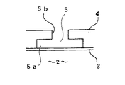
図1は本発明の製造方法によりレジスト被膜4が形成されたプリント配線板1の断面図を表すもので、基板2の表面に導体パターン3が形成されており、これの表面にレジスト被膜4が後述の工程を経て形成されている。このレジスト被膜4には所定の位置に開口部5が形成されている。
【0015】
尚、開口部5の形状は、図2及び図3に示す形状であってもて良い。
【0016】
次に、本発明に係るレジスト被膜の製造方法に関して説明する。図4に示すように、導体パターン3を前処理した後、その表面に液体レジストを印刷する。そして、これを紫外線で300〜900mJ露光する。
【0017】
つぎに、Na2CO3によるアルカリ現像を行い、この溶液をリンスした後、それぞれ5〜30秒間の水洗を数回行う。この水洗用の溶液は、イオン交換により生成された純水にCaCl2 を添加してCaイオン濃度を17〜20mg/Lにした水溶液が利用される。
【0018】
そして、液切りして乾燥し、最後に紫外線硬化、熱硬化を行う。
【0019】
つぎに、水洗溶液のCaイオン濃度とNaとの関係に関して説明する。図5は、Caイオン濃度とNa残渣量との関係を示す。これによれば、Caイオン濃度を17mg/L以上に設定すれば、Naの残渣量を0にすることができる。
【0020】
しかし、Caイオン濃度が20mg/Lであっても、水溶液を繰り返し使用すると、図6に示すようにNa残渣量は漸次増加するので、水溶液の使用限度を設定して常時管理する必要がある。
【0021】
【発明の効果】
請求項1及び2の発明は、導体パターンの表面に塗布した液体レジストを露光し、アルカリ現像・水洗・乾燥をした後、熱硬化するレジスト被膜の製造方法において、
アルカリ現像後の水洗用液のCaイオン濃度を17〜20mg/Lにしたので、現像液に含まれるNaを排除して、絶縁抵抗の低下を防止できるという優れた効果を奏するものである。
【0022】
請求項3及び4の水洗用液は、Caイオン濃度を17〜20mg/Lにしたので、アルカリ現像液に含まれるNaを排除して、絶縁抵抗の低下を防止できるという優れた効果を奏するものである。
【図面の簡単な説明】
【図1】 プリント配線板の断面図である。
【図2】 開口部の他の実施例における断面図である。
【図3】 開口部の異なる実施例における断面図である。
【図4】 レジスト被膜の製造工程を示す図である。
【図5】 水洗溶液のCaイオン濃度とNa残渣量の関係を示す図である。
【図6】 処理枚数に対するNa残渣量の関係を示す図である。
【符号の説明】
1 プリント配線板
2 基板
3 導体パターン
4 レジスト被膜
5 開口部
6 めっき膜[0001]
BACKGROUND OF THE INVENTION
The present invention relates to a method for producing a resist film and a washing solution for forming a resist film on a surface of a conductor pattern in the process of producing a printed wiring board.
[0002]
[Prior art]
Conventionally, in the process of manufacturing a printed wiring board, a liquid resist is applied to the surface of a conductor pattern, exposed, then subjected to alkali development with Na 2 CO 3 , washed with water several times, and then thermally cured. A resist film is formed.
[0003]
The water used for this washing is generally used by drawing up groundwater.
[0004]
However, in recent years, groundwater has become scarce and components have become unstable, so that it is not possible to use groundwater as it is in order to maintain the quality of printed wiring boards.
[0005]
Therefore, manufacturers use pure water (hereinafter simply referred to as ionic water) generated by ion exchange by constructing an ion tower.
[0006]
[Problems to be solved by the invention]
However, when the above-described washing with ionic water is performed, a new problem that the insulation resistance of the printed wiring board is reduced occurs.
[0007]
As a result of various investigations regarding this cause, it was found that Na in alkali development was not completely eliminated. Na ions cause insulation failure even in a very small amount.
[0008]
This invention is made | formed in view of said situation, The objective is to provide the manufacturing method of a resist film, and the washing | cleaning liquid which do not have a possibility that the insulation resistance of a printed wiring board may fall.
[0009]
[Means for Solving the Problems]
Means taken by the present invention to solve this problem will be described with reference numerals used in the embodiments. The invention of claim 1 exposes the
Since the Ca ion concentration of the washing solution after alkali development is 17 to 20 mg / L, it is possible to eliminate Na contained in the developer and prevent a decrease in insulation resistance.
[0010]
In addition, Ca, Mg, Sr, Ba, and Ra were also effective in the above concentration range.
The invention of
[0011]
The invention of
[0012]
The invention of
[0013]
DETAILED DESCRIPTION OF THE INVENTION
Hereinafter, an embodiment of the present invention will be described with reference to the drawings.
[0014]
FIG. 1 shows a cross-sectional view of a printed wiring board 1 on which a
[0015]
The shape of the
[0016]
Next, a method for producing a resist film according to the present invention will be described. As shown in FIG. 4, after the
[0017]
Next, alkali development with Na 2 CO 3 is performed, and the solution is rinsed, followed by washing with water for 5 to 30 seconds several times. As this washing solution, an aqueous solution in which CaCl 2 is added to pure water generated by ion exchange to have a Ca ion concentration of 17 to 20 mg / L is used.
[0018]
Then, the liquid is drained and dried, and finally UV curing and heat curing are performed.
[0019]
Next, the relationship between the Ca ion concentration of the water washing solution and Na will be described. FIG. 5 shows the relationship between the Ca ion concentration and the amount of Na residue. According to this, if the Ca ion concentration is set to 17 mg / L or more, the amount of Na residue can be reduced to zero.
[0020]
However, even if the Ca ion concentration is 20 mg / L, if the aqueous solution is repeatedly used, the amount of Na residue gradually increases as shown in FIG.
[0021]
【The invention's effect】
Invention of
Since the Ca ion concentration of the washing solution after alkali development is set to 17 to 20 mg / L, an excellent effect is obtained in that Na contained in the developer is excluded and a decrease in insulation resistance can be prevented.
[0022]
Since the washing solution according to
[Brief description of the drawings]
FIG. 1 is a cross-sectional view of a printed wiring board.
FIG. 2 is a cross-sectional view of another embodiment of the opening.
FIG. 3 is a cross-sectional view of different examples of openings.
FIG. 4 is a diagram showing a resist film manufacturing process.
FIG. 5 is a graph showing the relationship between the Ca ion concentration of a water washing solution and the amount of Na residue.
FIG. 6 is a diagram showing the relationship of the amount of Na residue to the number of processed sheets.
[Explanation of symbols]
1 Printed
Claims (4)
アルカリ現像後のNaイオンを排除して、絶縁抵抗の低下を防止するために、水洗用液のCaイオン濃度を17〜20mg/Lにしたことを特徴とするレジスト被膜の製造方法。In the method for producing a resist film that is thermally cured after exposing the liquid resist applied to the surface of the conductor pattern with ultraviolet light, performing alkali development, washing with water, and drying,
A method for producing a resist film, characterized in that the Na ion after alkali development is excluded to prevent a decrease in insulation resistance, and the Ca ion concentration of the washing solution is 17 to 20 mg / L.
Priority Applications (1)
| Application Number | Priority Date | Filing Date | Title |
|---|---|---|---|
| JP01039799A JP4075005B2 (en) | 1999-01-19 | 1999-01-19 | Method for producing resist film and washing solution |
Applications Claiming Priority (1)
| Application Number | Priority Date | Filing Date | Title |
|---|---|---|---|
| JP01039799A JP4075005B2 (en) | 1999-01-19 | 1999-01-19 | Method for producing resist film and washing solution |
Publications (2)
| Publication Number | Publication Date |
|---|---|
| JP2000208904A JP2000208904A (en) | 2000-07-28 |
| JP4075005B2 true JP4075005B2 (en) | 2008-04-16 |
Family
ID=11749013
Family Applications (1)
| Application Number | Title | Priority Date | Filing Date |
|---|---|---|---|
| JP01039799A Expired - Fee Related JP4075005B2 (en) | 1999-01-19 | 1999-01-19 | Method for producing resist film and washing solution |
Country Status (1)
| Country | Link |
|---|---|
| JP (1) | JP4075005B2 (en) |
Families Citing this family (3)
| Publication number | Priority date | Publication date | Assignee | Title |
|---|---|---|---|---|
| JP4267974B2 (en) * | 2003-07-10 | 2009-05-27 | 日本メクトロン株式会社 | Circuit board and manufacturing method thereof |
| JP4706188B2 (en) * | 2004-05-12 | 2011-06-22 | 日立化成工業株式会社 | Use of photosensitive resin composition |
| JP2012208356A (en) * | 2011-03-30 | 2012-10-25 | Kyocer Slc Technologies Corp | Method for developing photosensitive resin |
-
1999
- 1999-01-19 JP JP01039799A patent/JP4075005B2/en not_active Expired - Fee Related
Also Published As
| Publication number | Publication date |
|---|---|
| JP2000208904A (en) | 2000-07-28 |
Similar Documents
| Publication | Publication Date | Title |
|---|---|---|
| CN108541142B (en) | PCB inner layer circuit pattern transfer process | |
| KR20200000700U (en) | Printed wiring board | |
| KR100749444B1 (en) | Method for producing etched circuits | |
| JP4075005B2 (en) | Method for producing resist film and washing solution | |
| JP3080366B2 (en) | Electroless metal plating method and circuitized structure | |
| CN113973440A (en) | Circuit board insulating layer treatment process | |
| US5773198A (en) | Method of forming high resolution circuitry by depositing a polyvinyl alcohol layer beneath a photosensitive polymer layer | |
| CN112004329A (en) | Processing method for preventing false copper exposure of circuit board | |
| US4230794A (en) | Improving etch resistance of a casein-based photoresist | |
| JP2000156556A (en) | Method for forming resist layer on substrate having through hole part and production of printed wiring board | |
| JP3209290U (en) | Printed wiring board | |
| KR100251831B1 (en) | Via hole forming method of multiple printed circuit board | |
| JP2004218033A (en) | Etching product and etching method | |
| GB2087157A (en) | Solder plating printed circuit boards | |
| JP3663987B2 (en) | Method for manufacturing printed wiring board | |
| JP2002185138A (en) | Method of manufacturing multilayer wiring board | |
| JPH06177516A (en) | Manufacture of printed wiring board | |
| JPH1168297A (en) | Production of circuit board | |
| JP4392677B2 (en) | Printed wiring board | |
| CN108243571A (en) | The manufacturing method of flexible PCB | |
| JP2000236160A (en) | Forming method of and washing fluid for resist coat | |
| JPS61139089A (en) | Manufacture of printed wiring board | |
| JPH0353587A (en) | Formation of resist pattern | |
| JPH02196494A (en) | Manufacture of printed wiring board for surface mounting | |
| JP3191686B2 (en) | Manufacturing method of printed wiring board |
Legal Events
| Date | Code | Title | Description |
|---|---|---|---|
| A621 | Written request for application examination |
Free format text: JAPANESE INTERMEDIATE CODE: A621 Effective date: 20051207 |
|
| A131 | Notification of reasons for refusal |
Free format text: JAPANESE INTERMEDIATE CODE: A131 Effective date: 20070813 |
|
| A521 | Written amendment |
Free format text: JAPANESE INTERMEDIATE CODE: A523 Effective date: 20071011 |
|
| A521 | Written amendment |
Free format text: JAPANESE INTERMEDIATE CODE: A523 Effective date: 20071030 |
|
| RD02 | Notification of acceptance of power of attorney |
Free format text: JAPANESE INTERMEDIATE CODE: A7422 Effective date: 20071030 |
|
| TRDD | Decision of grant or rejection written | ||
| A01 | Written decision to grant a patent or to grant a registration (utility model) |
Free format text: JAPANESE INTERMEDIATE CODE: A01 Effective date: 20080115 |
|
| A61 | First payment of annual fees (during grant procedure) |
Free format text: JAPANESE INTERMEDIATE CODE: A61 Effective date: 20080118 |
|
| R150 | Certificate of patent or registration of utility model |
Free format text: JAPANESE INTERMEDIATE CODE: R150 |
|
| FPAY | Renewal fee payment (event date is renewal date of database) |
Free format text: PAYMENT UNTIL: 20110208 Year of fee payment: 3 |
|
| FPAY | Renewal fee payment (event date is renewal date of database) |
Free format text: PAYMENT UNTIL: 20110208 Year of fee payment: 3 |
|
| FPAY | Renewal fee payment (event date is renewal date of database) |
Free format text: PAYMENT UNTIL: 20120208 Year of fee payment: 4 |
|
| FPAY | Renewal fee payment (event date is renewal date of database) |
Free format text: PAYMENT UNTIL: 20130208 Year of fee payment: 5 |
|
| FPAY | Renewal fee payment (event date is renewal date of database) |
Free format text: PAYMENT UNTIL: 20140208 Year of fee payment: 6 |
|
| R250 | Receipt of annual fees |
Free format text: JAPANESE INTERMEDIATE CODE: R250 |
|
| R250 | Receipt of annual fees |
Free format text: JAPANESE INTERMEDIATE CODE: R250 |
|
| LAPS | Cancellation because of no payment of annual fees |