JP4065503B2 - Image processing apparatus, image input / output apparatus, scaling process method, and memory control method - Google Patents
Image processing apparatus, image input / output apparatus, scaling process method, and memory control method Download PDFInfo
- Publication number
- JP4065503B2 JP4065503B2 JP2002202918A JP2002202918A JP4065503B2 JP 4065503 B2 JP4065503 B2 JP 4065503B2 JP 2002202918 A JP2002202918 A JP 2002202918A JP 2002202918 A JP2002202918 A JP 2002202918A JP 4065503 B2 JP4065503 B2 JP 4065503B2
- Authority
- JP
- Japan
- Prior art keywords
- scaling
- tile
- image
- data
- unit
- Prior art date
- Legal status (The legal status is an assumption and is not a legal conclusion. Google has not performed a legal analysis and makes no representation as to the accuracy of the status listed.)
- Expired - Fee Related
Links
Images


Classifications
-
- G—PHYSICS
- G06—COMPUTING; CALCULATING OR COUNTING
- G06T—IMAGE DATA PROCESSING OR GENERATION, IN GENERAL
- G06T3/00—Geometric image transformation in the plane of the image
- G06T3/40—Scaling the whole image or part thereof
Landscapes
- Physics & Mathematics (AREA)
- General Physics & Mathematics (AREA)
- Engineering & Computer Science (AREA)
- Theoretical Computer Science (AREA)
- Image Processing (AREA)
- Editing Of Facsimile Originals (AREA)
Description
【0001】
【発明の属する技術分野】
本発明は、入力した画像データに画像処理、特に変倍処理を施すための画像処理装置、画像入出力装置、変倍処理方法、及びメモリ制御方法に関する。
【0002】
【従来の技術】
画像の変倍処理は、デジタル複写機等の画像入出力装置や、パーソナルコンピュータ等の情報処理装置において、非常に重要な機能となっている。特に画像入出力装置においては、頻繁に用いられる機能であり、通常、専用の変倍回路が設けられている。
【0003】
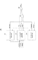
従来の変倍回路の動作概略を図34に示す。図34において、3401は変倍回路を示し、3402は変倍される原画像(入力画像)全体を、3403は変倍後の出力画像全体を示している。また、3404は変倍前、3405は変倍後の画像の各画素を示している。各画像の内部に示された各番号は変倍回路3401に入力或いは出力される順番を示す。
【0004】
図35は、従来の変倍回路3401の詳細な構成を示すブロック図である。図35において、3501はラインバッファ、3502は垂直フィルタ、3503はシフトレジスタ、3504は水平フィルタである。水平及び垂直フィルタの詳細な構成については図36に示す。
【0005】
図34に示す従来の変倍回路3401は、1枚の画像における画像データ(ピクセルデータ)をスキャン順に受け取って、変倍結果をスキャン順に出力する。この変倍回路3401の内部における処理について図35を用いて説明する。まず、外部から変倍回路3401に入力されたピクセルデータは、ラインバッファ3501に蓄積される。そして、垂直フィルタ3502は水平方向に一致した位置でかつ垂直方向が1ラインずつシフトさせた複数の画像データ(図35では8ライン分)のフィルタ処理を行う。垂直方向のフィルタ処理を行った後、その結果の画像データは水平方向の変倍処理を行うべくシフトレジスタ3503に入力され、垂直方向と同様に画像データ(図35では8画素)フィルタ処理が行われる。
【0006】
図36は、フィルタ処理回路の動作を示す図である。図36において、3601はフィルタ係数発生回路、3602は乗算回路、3603は加算回路である。ここで、フィルタ係数発生回路3601からフィルタ係数が出力され、一方で、垂直或いは水平方向に連続した画像データが、ラインバッファ3501或いはシフトレジスタ3503から入力される。そして、画像データの各々の画素と、その画素に対応するフィルタ係数との掛け算を乗算回路3602で行った後、すべての演算結果が加算回路3603で加算されて出力される。以上が従来の変倍処理の構成である。
【0007】
ところで、特開平2002−8002号公報に開示されるように、各処理ブロックがタイル単位で画像処理を行う画像入出力装置が本出願人より提案されている。この画像入出力装置の画像処理部の構成はICチップ化に適しており、その処理ブロックの一つとして変倍回路を備えることができる。
【0008】
【発明が解決しようとする課題】
しかしながら、昨今の取り扱う画像サイズの巨大化に伴い、上記従来例のような変倍回路では、変倍処理に必要なバッファが非常に大きなものとなる。図35の回路の場合、ラインバッファは8ライン分必要なので、例えばA4、600dpiの原画像の場合、約7000画素分のバッファが必要となる。
【0009】
そして、特に上述したタイル単位で画像データを管理する画像入出力装置に変倍回路を実装する場合、従来の変倍回路では、1つのチップ内に変倍回路を組み込もうとしても、ラインバッファも巨大なものとなるので、IC化に際しては現実的ではなかった。
【0010】
また、変倍回路を含むICチップにラインバッファを持たず、管理可能なチップ外部のメモリをラインバッファの代わりとして利用する装置構成も考えられるが、この構成のみでは、外部メモリへのアクセスが集中し、変倍回路の処理速度が制限されることがある。
【0011】
本発明は上述した問題点を解決するためのものであり、少ないメモリ容量でタイル単位に変倍処理を行える画像処理装置及び画像処理装置の変倍処理方法を提供することを目的とする。
【0012】
また、外部メモリを用いた画像処理、特に変倍処理を行う際の処理速度を向上させた画像処理装置及び画像処理装置のメモリ制御方法を提供することを目的とする。
【0013】
また、簡単な構成で変倍処理と画像データの書き込み処理を行う際のメモリ管理を容易に効率よく行える画像処理装置及び画像処理装置のメモリ制御方法を提供することを目的とする。
【0014】
また、回路のクロック速度を上げることなく、変倍処理を行う際の処理速度を向上させた画像処理装置及び画像処理装置の変倍処理方法を提供することを目的とする。
【0015】
また、外部メモリを用いた変倍処理におけるデータ管理を容易にした画像入出力装置及び画像入出力装置の変倍処理法を提供することを目的とする。
【0016】
また、ICチップ内の回路構成にはほとんど影響を与えることなく、様々な変倍率や画像サイズに対応した変倍処理を可能とした画像入出力装置及び画像入出力装置の変倍処理法を提供することを目的とする。
【0017】
【課題を解決するための手段】
上記目的を達成するために、本発明の画像処理装置は、入力した画像データに変倍処理を施す画像処理装置であって、入力した画像データを分割処理して所定の大きさの複数のタイル画像データを生成する分割手段と、前記分割手段により生成された複数のタイル画像データを圧縮処理して該圧縮処理されたタイル画像データを含む複数のデータパケットを生成する圧縮手段と、前記圧縮手段により生成された複数のデータパケットを記憶する記憶手段と、前記記憶手段に記憶された複数のデータパケットの各々に含まれるタイル画像データを読み出して伸張処理する伸張手段と、前記伸張手段により伸張処理された複数のデータパケットに基づく複数のタイル画像データを変倍処理して前記所定の大きさの複数のタイル画像データを生成する変倍手段と、前記記憶手段に記憶された複数のデータパケットに基づいて前記変倍処理を実行させる場合に、前記伸張手段、前記変倍手段、前記圧縮手段、前記記憶手段の順で前記複数のデータパケットを転送させるためのヘッダ情報を前記複数のデータパケットに付加する付加手段とを有し、前記伸張手段は前記記憶手段に記憶された複数のデータパケットの各々に含まれるタイル画像データを伸張処理して、該伸張処理されたタイル画像データを含む複数のデータパケットを前記ヘッダ情報に基づいて前記変倍手段へ転送し、前記変倍手段は前記伸張手段から転送された前記複数のデータパケットの各々に含まれるタイル画像データを変倍処理して、該変倍処理により生成されたタイル画像データを含む複数のデータパケットを前記ヘッダ情報に基づいて前記圧縮手段へ転送し、前記圧縮手段は、前記変倍手段から転送された前記複数のデータパケットの各々に含まれるタイル画像データを圧縮処理して、該圧縮処理されたタイル画像データを含む複数のデータパケットを前記ヘッダ情報に基づいて前記記憶手段に転送することを特徴とする。
【0023】
また、本発明の変倍処理方法は、変倍処理を実行する変倍部と、圧縮処理を実行する圧縮部と、伸張処理を実行する伸張部とを有する画像処理装置の変倍処理方法であって、入力した画像データを分割処理して所定の大きさの複数のタイル画像データを生成する分割工程と、前記分割工程により生成された複数のタイル画像データを前記圧縮部にて圧縮処理して該圧縮処理されたタイル画像データを含む複数のデータパケットを生成する第1圧縮工程と、前記第1圧縮工程により生成された複数のデータパケットをメモリに書き込む第1書込工程と、前記メモリに記憶された複数のデータパケットに基づいて前記変倍処理を実行させる場合に、前記伸張部、前記変倍部、前記圧縮部、前記メモリの順で前記複数のデータパケットを転送させるためのヘッダ情報を前記複数のデータパケットに付加する付加工程と、前記メモリに書き込まれた複数のデータパケットの各々に含まれるタイル画像データを前記伸張部にて伸張処理して、該伸張処理されたタイル画像データを含む複数のデータパケットを前記ヘッダ情報に基づいて前記変倍部へ転送する伸張工程と、前記伸張工程により前記伸張部から前記変倍部に転送された前記複数のデータパケットの各々に含まれるタイル画像データを前記変倍部にて変倍処理して該変倍処理により生成された前記所定の大きさのタイル画像データを含む複数のデータパケットを前記ヘッダ情報に基づいて前記圧縮部に転送する変倍工程と、前記変倍工程により前記変倍部から前記圧縮部に転送された前記複数のデータパケットの各々に含まれるタイル画像データを圧縮処理して該圧縮処理されたタイル画像データを含む複数のデータパケットを前記ヘッダ情報に基づいて前記メモリに転送する第2圧縮工程と、前記第2圧縮工程にて前記圧縮部から前記メモリに転送された前複数のデータパケットを前記メモリに書き込む第2書込工程と、を有することを特徴とする。
【0025】
また、本発明の変倍処理方法は、入力した画像データに変倍処理を施す画像処理装置のメモリ制御方法であって、入力した画像データを分割処理してメモリに複数のタイル画像データを書き込む書込工程と、前記メモリに書き込まれたタイル画像データを読み出す読出工程と、
前記読出工程において読み出されたタイル画像データを変倍処理する変倍工程と、指定された垂直方向の変倍率がn(n<1)である場合、前記メモリにおいて管理すべき垂直方向のタイル画像データの数を少なくとも(1/n)+2個とし、前記読出工程及び前記書込工程における前記メモリへのアクセスに関する排他制御を行う排他制御工程とを有することを特徴とする。
【0029】
【発明の実施の形態】
以下、図面を参照しながら本発明に係る実施の形態を詳細に説明する。
【0030】
(第1の実施形態)
まず、1枚の画像を複数のタイルに分割し、タイル単位で画像データを授受し管理する画像入出力装置の構成及び動作について説明する。この画像入出力装置は、一般にデジタル複写機と呼ばれるものであり、本発明に係る変倍処理を実行することができる。
【0031】
[画像入出力装置の構成]
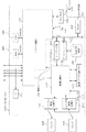
図1は、本発明を適用可能な画像入出力装置(デジタル複写機)の構成を説明するブロック図である。図2は、図1に示すシステム制御部の構成を説明する詳細ブロック図であり、図3は、図1に示す画像処理部の構成を説明する詳細ブロック図である。
【0032】
図1〜図3において、ControllerUnit2000は画像入力デバイスであるスキャナ2070や画像出力デバイスであるプリンタ2095と接続し、一方ではLAN2011や公衆回線(WAN)2051と接続することで、画像情報やデバイス情報の入出力、PDLデータのイメージ展開を行う為のコントローラである。
【0033】
図2において、CPU2001はシステム全体を制御するプロセッサである。本実施形態では2つのCPUを用いた例を示す。これら二つのCPUは、共通のCPUバス2126に接続され、さらに、システムバスブリッジ2007に接続される。
【0034】
システムバスブリッジ2007は、バススイッチであり、CPUバス2126、RAMコントローラ2124、ROMコントローラ2125、IOバス2127、サブバススイッチ2128、IOバス2129、画像リングインタフェース(1)2147、画像リングインタフェース(2)2148が接続される。
【0035】
サブバススイッチ2128は、第二のバススイッチであり、画像DMA(1)2130、画像DMA(2)2132、フォント伸張部2134、ソート回路2135、ビットマップトレース部2136が接続され、これらのDMAから出力されるメモリアクセス要求を調停し、システムバスブリッジへの接続を行う。
【0036】
図1において、RAM2002は、CPU2001が動作するためのシステムワークメモリであり、画像データを一時記憶するための画像メモリでもある。RAM2002は、図2のRAMコントローラ2124により制御され、本実施形態では、ダイレクトRDRAMを採用する例を示す。
【0037】
ROM2003はブートROMであり、システムのブートプログラムが格納されている。ROM2003は、図2のROMコントローラ2125により制御される。
【0038】
図2において、画像DMA(1)2130は、画像圧縮部2131に接続し、レジスタアクセスリング2137を介して設定された情報に基づき、画像圧縮部2131を制御し、RAM2002上にある非圧縮データの読み出し、圧縮、圧縮後データの書き戻しを行う。本実施形態では、JPEGを圧縮アルゴリズムに採用した例を示す。
【0039】
画像DMA(2)2132は、画像伸長部2133に接続し、レジスタアクセスリング2137を介して設定された情報に基づき、画像伸長部2133を制御し、RAM2002上にある圧縮データの読み出し、伸長、伸長後データの書き戻しを行う。本実施形態では、JPEGを伸長アルゴリズムに採用した例を示す。
【0040】
フォント伸長部2134は、LANインタフェース2010等を介し外部より転送されるPDLデータに含まれるフォントコードに基づき、ROM2003もしくは、RAM2002内に格納された、圧縮フォントデータの伸長を行う。本実施形態では、FBEアルゴリズムを採用した例を示す。
【0041】
ソート回路2135は、PDLデータを展開する段階で生成されるディスプレイリストのオブジェクトの順番を並び替える回路である。ビットマップトレース回路2136は、ビットマップデータより、エッジ情報を抽出する回路である。
【0042】
IOバス2127は、内部IOバスの一種であり、標準バスであるUSBバスのコントローラ、USBインタフェース2138、汎用シリアルポート2139、インタラプトコントローラ2140、GPIOインタフェース2141が接続される。IOバス2127には、バスアービタ(図示せず)が含まれる。
【0043】
操作部I/F2006は、図1の操作部(UI)2012のインタフェース部で、操作部2012に表示する画像データを操作部2012に対して出力する。また、操作部2012から本システム使用者が入力した情報を、CPU2001に伝える役割をする。
【0044】
IOバス2129は内部IOバスの一種であり、汎用バスインタフェース(1,2)2142と、LANコントローラ2010が接続される。IOバス2129にはバスアービタ(図示せず)が含まれる。
【0045】
汎用バスインタフェース(1,2)2142は、2つの同一のバスインタフェースから成り、標準IOバスをサポートするバスブリッジである。本実施形態では、PCIバス2143,2153を採用した例を示す。
【0046】
図1において、2004はハードディスクドライブ(HDD)で、システムソフトウェア、画像データを格納する。HDD2004は、ディスクコントローラ2144を介して一方のPCIバス2153に接続される。
【0047】
図2のLANコントローラ2010は、MAC回路2145、PHY/PMD回路2146を介しLAN2011に接続し、情報の入出力を行う。Modem2050は公衆回線2051に接続し、情報の入出力を行う。
【0048】
図2において、画像リングインタフェース(1)2147及び画像リングインタフェース(2)2148は、システムバスブリッジ2007と画像データを高速で転送する画像リング2008を接続し、タイル化後に圧縮されたデータをRAM2002とタイル画像処理部2149間で転送するDMAコントローラである。
【0049】
画像リング2008は、一対の単方向接続経路の組み合わせにより構成される。図3に示すように、画像リング2008は、タイル画像処理部2149内で、画像リングインタフェース(3)2101及び画像リングインタフェース(4)2102を介し、タイル伸長部(1,2)2103、コマンド処理部2104、ステータス処理部2105、タイル圧縮部(1−3)2106に接続される。本実施形態では、タイル伸長部2103を2組、タイル圧縮部2106を3組実装する例を示す。
【0050】
タイル伸長部(1,2)2103は、画像リングインタフェース(3)2101への接続に加え、タイルバス2107に接続され、画像リングより入力された圧縮後の画像データを伸長し、タイルバス2107へ転送するバスブリッジである。本実施形態では、JPEG及びパックビッツ方式による伸長アルゴリズムを採用した例を示す。
【0051】
タイル圧縮部(1−3)2106は、画像リングインタフェース(4)2102への接続に加え、タイルバス2107に接続され、タイルバス2107より入力された圧縮前の画像データを圧縮し、画像リング2008へ転送するバスブリッジである。本実施形態では、タイル伸長部と同じ様にJPEG及びパックビッツ方式による圧縮アルゴリズムを採用した例を示す。
【0052】
コマンド処理部2104は、画像リングインタフェースへの接続に加え、レジスタ設定バス2109に接続され、画像リングを介して入力したCPU2001より発行されたレジスタ設定要求を、レジスタ設定バス2109に接続される該当ブロックへ書き込む。また、CPU2001より発行されたレジスタ読み出し要求に基づき、レジスタ設定バスを介して該当レジスタより情報を読み出し、画像リングインタフェース2102に転送する。
【0053】
ステータス処理部2105は、各画像処理部の情報を監視し、CPU2001に対してインタラプトを発行するためのインタラプトパケットを生成し、画像リングインタフェース2102に出力する。タイルバス2107には上記ブロックに加え、以下の機能ブロックが接続される。
【0054】
レンダリング部インタフェース2110、画像入力インタフェース2112、画像出力インタフェース2113、多値化部2119、2値化部2118、色空間変換部2117、画像回転部2030、変倍処理部2116、レンダリング部インターフェース2110。
【0055】
レンダリング部インターフェース2110は、後述するレンダリング部2060により生成されたビットマップイメージを入力するインタフェースとして機能をする。レンダリング部2060とレンダリング部インタフェース2110は、一般的なビデオ信号2111にて接続される。レンダリング部インタフェース2110は、タイルバス2107に加え、メモリバス2108、レジスタ設定バス2109へ接続される。そして、レンダリング部インタフェース2110は、レジスタ設定バス2109を介して設定された所定の方法により、入力されたラスタ画像をタイル画像へ構造変換するとともにクロックの同期化を行い、タイルバス2107に対しタイル画像の出力を行う。
【0056】
画像入力インタフェース2112は、後述するスキャナ用画像処理部2114により補正画像処理されたラスタイメージデータを入力する。そして、画像入力インタフェース2112は、レジスタ設定バス2109を介して設定された所定の方法により、入力したラスタイメージデータをタイル画像へ構造変換するとともにクロックの同期化を行い、タイルバス2107に対しタイル画像の出力を行う。
【0057】
画像出力インタフェース2113は、タイルバスからのタイル画像データ(データパケット)を入力し、入力したタイル画像データをラスタ画像へ構造変換するとともにクロックレートの変更を行い、ラスタ画像をプリンタ用画像処理部2115へ出力する。
【0058】
画像回転部2030は画像データの回転を行う。変倍処理(解像度変換)部2116は画像の変倍処理(解像度の変更)を行う。変倍部2116は、本実施形態における主要部であり、その詳細については後述する。色空間変換部2117はカラー及びグレースケール画像の色空間の変換を行う。2値化部2118は、多値(カラー、グレースケール)画像を2値化する。多値化部2119は2値画像を多値データへ変換する。
【0059】
外部バスインタフェース部2120は、画像リングインタフェース(1)2147、(3)2101、コマンド処理部2104、レジスタ設定バス2109を介し、CPU2001により発行された、書き込み、読み出し要求を外部バス2121に変換出力するバスブリッジである。外部バス2121は本実施形態では、プリンタ用画像処理部2115、スキャナ用画像処理部2114に接続されている。
【0060】
メモリ制御部2122は、メモリバス2108に接続され、各画像処理部の要求に従い、あらかじめ設定されたアドレス分割により、画像メモリ(1,2)2123に対して、画像データの書き込み、読み出し、必要に応じてリフレッシュ等の動作を行う。本実施形態では、画像メモリにSDRAMを用いた例を示す。
【0061】
図1において、スキャナ用画像処理部2114は、画像入力デバイスであるスキャナ2070によりスキャンされた画像データを補正画像処理する。
【0062】
プリンタ用画像処理部2115では、プリンタ出力のための補正画像処理を行い、結果をプリンタ2095へ出力する。レンダリング部2060はPDLコードもしくは、中間ディスプレイリストをビットマップイメージに展開する。
【0063】
[画像入出力装置のユニット構成]
図1の画像入出力装置のContoroller Unit2000は、1つのコントローラボードに構成されている。そして、システム制御部2150、及び画像処理部2149は、このボード上にそれぞれICチップとして実装されている。この2つのICチップ間のデータ転送は、画像リングを介して、後述の各パケットにより行なわれる。
【0064】
また、画像メモリ(1,2)2123は、画像処理部2149の外部メモリとして、同じくコントローラボード上に独立して設けられている。本実施形態において、このメモリは、ボード上のメモリスロットに対して着脱可能なカードの形態を有しており、必要に応じて異なる容量の別のメモリに差し替えることもできる。なお、画像メモリ2123は、カードの形態に限らず、コントローラボードに直接埋め込まれるICチップの形態を有していてもよい。
【0065】
[ネットワークシステムの構成]
図4は、図1の画像入出力装置(デジタル複写機)を含むネットワークシステム全体の構成を説明する図である。
【0066】
図4において、1001は図1の画像入出力装置であり、スキャナとプリンタから構成され、スキャナから読み込んだ画像をローカルエリアネットワーク(以下LAN)1010に流したり、LANから受信した画像をプリンタによりプリントアウトできる。また、スキャナから読み込んだ画像を図示しないFAX送信手段により、PSTNまたはISDN1030に送信したり、PSTNまたはISDNから受信した画像をプリンタによりプリントアウトできる。1002は、データベースサーバで、画像入出力装置1001により読み込んだ2値画像及び多値画像をデータベースとして管理する。
【0067】
1003は前記データベースサーバ1002のデータベースクライアントで、データベースサーバ1002に保存されている画像データを閲覧/検索等できる。
【0068】
1004は電子メールサーバで、画像入出力装置1001により読み取った画像を電子メールの添付として受け取ることができる。1005は、電子メールクライアントで、電子メールサーバ1004の受け取ったメールを受信し閲覧したり、電子メールを送信したりすることが可能である。
【0069】
1006はHTML文書をLANに提供するWWWサーバで、画像入出力装置1001によりWWWサーバで提供されるHTML文書をプリントアウトできる。
【0070】
1007はルータで、LAN1010をインターネット/イントラネット1012と連結する。インターネット/イントラネットに、前述したデータベースサーバ1002、WWWサーバ1006、電子メールサーバ1004、画像入出力装置1001と同様の装置が、それぞれ1020、1021、1022、1023として連結している。
【0071】
一方、画像入出力装置1001は、PSTNまたはISDN1030を介して、FAX装置1031と送受信可能になっている。
【0072】
また、LAN上にプリンタ1040も連結されており、画像入出力装置1001により読み取った画像をプリントアウト可能なように構成されている。
【0073】
[パケット構成]
次に、本実施形態における画像データ処理に用いられるパケットのフォーマットについて説明する。本実施形態におけるControllerUnit2000は、画像データ、CPU2001によるコマンド、及び各画像処理部(2116,2117,2118,2119,2030)より発行される割り込み情報を、パケット化された形式で転送する。パケットデータには、以下の種類がある。
【0074】
(1)データパケット(図5)
図5に示すデータパケットは所定画素数(本実施形態では32pixel×32pixelとする)で分割したタイル単位の画像データ3002と、後述する制御情報を格納するヘッダ情報3001と画像付加情報等3003とから構成される。
【0075】
以下、ヘッダ情報3001内に含まれる情報について説明を行う。
【0076】
PcktType3004はパケット・タイプを識別する。このPcktType3004にはリピートフラグが含まれており、画像データ3002が1つ前に送信したデータパケットの画像データと同一の場合、リピートフラグがセットされる。
【0077】
ChipID3005はパケットの送信先のChipを示す。ImageType3006は画像データのタイプを示す。PageID3007は画像データのページ番号を示す。JobID3008はソフトウェアで画像処理を管理するためのジョブIDを格納する。PacketIDY3009及びPacketIDX3010は、パケットに含まれる(又は指定される)画像データが、画像全体においてどの位置におけるタイルに相当するかを示す。ここでタイル位置はY方向(PacketIDY3009)とX方向(PacketIDX3010)を組み合わせ、YnXnで表される。
【0078】
データパケットは画像データが圧縮されている場合と非圧縮の場合とがある。本実施形態では、圧縮アルゴリズムとして、多値カラー(多値グレースケールを含む)の場合はJPEGを、2値の場合はパックビッツを採用した例を示した。圧縮されている場合と非圧縮の場合との区別は、後述するCompressFlag3017で示される。
【0079】
Process Instruction3011は5ビットのUnitID3019と3ビットのMode3020との組である処理Unit1−8から構成され、各処理Unitは左(下位)から順番に処理される。処理されたUnitID及びModeは廃棄され、次に処理されるUnitID及びModeが左端に位置するように、Process Instruction全体が左に8ビットシフトされる。Process Instruction3011にはUnitID3019とMode3020との組が最大8組格納される。UnitID3019は各画像データ処理部を指定し、Mode3020は各画像データ処理部での動作モードを指定する。これにより、1つの画像データパケットに含まれる(又は指定される)画像データに対して、最大でのべ8つの画像データ処理部による連続処理を指定することが可能である。
【0080】
PacketByteLength3012はパケットのトータルバイト数を示す。ImageDataByteLengh3015は画像データのバイト数を示す。ZDataByteLength3016は画像付加情報のバイト数を示す。ImageDataOffset3013、ZDataOffset3014はそれぞれ、画像データ及び画像付加情報の、パケットの先頭からのオフセットを示す。
【0081】
(2)コマンドパケット(図6)
図6に示すコマンドパケットはレジスタ設定バス2109へのアクセスを行うためのものである。このパケットを用いることにより、CPU2001より画像メモリ(1,2)2123へのアクセスも可能である。また、コマンドパケットは、ヘッダ4001及びコマンド(パケットデータ部)4002から構成される。
【0082】
このヘッダ4001におけるChipID4004には、コマンドパケットの送信先となる画像処理部2149を表すIDが格納される。
【0083】
PageID4007及びJobID4008はそれぞれ、ソフトウェアで管理するためのPage ID及びJob IDを格納する。Packet ID4009は1次元で表され、Data PacketのX−coordinateのみを使用する。PacketByteLength4010は128Byte固定である。
【0084】
一方、パケットデータ部4002には、アドレス4011とデータ4012の組を1つのコマンドとして最大12個のコマンドを格納することが可能である。ライトかリードかのコマンドのタイプはCmdType4005で示され、コマンドの数はCmdnum4006で示される。
【0085】
(3)インタラプトパケット(図7)
図7に示すインタラプトパケットはヘッダ5001及びインタラプトデータ(パケットデータ部)5002からなり、画像処理部2149からCPU2001への割り込みを通知するために用いられる。
【0086】
ステータス処理部2105はインタラプトパケットを送信すると、次に送信の許可がされるまではインタラプトパケットを送信してはならない。PacketByteLength5006は128Byte固定である。
【0087】
パケットデータ部5002には、画像処理部2149の各々の内部モジュールのステータス情報5007が格納されている。ステータス処理部2105は画像処理部2149内のモジュールのステータス情報を集め、一括してシステム制御部2150に送ることができる。
【0088】
ChipID5004には、インタラプトパケットの送信先となるシステム制御部2150を表すIDが格納される。また、IntChipID5005にはインタラプトパケットの送信元となる画像処理部2149を表すIDが格納される。
【0089】
[パケットテーブルの構成]
上述した各パケットは、図8に示すようなパケットテーブル6001によって管理される。このパケットテーブル6001は画像データと対で使用され、画像データが図1に示すRAM2002に展開されている場合は、RAM2002上で管理される。また、画像データが外部記憶装置2004に格納される場合には、このパケットテーブル6001も同時に外部記憶装置2004に格納される。外部記憶装置2004に格納された画像データが再びRAM2002に展開される場合、同時にこのパケットテーブル6001もRAM2002に読み出され、画像データが展開されるアドレス情報に応じてアドレス情報の書き換えが行われる。
【0090】
パケットテーブル6001の値(ポインタ及び長さ)に0を5bit付加すると、パケットの先頭Address(Packet Start Address)6002、パケットのバイト長(Packet Byte Length)6005となる。即ち、
Packet Address Pointer (27bit) + 5b00000 = Packet先頭Address
PacketLength (11bit) + 5b00000 = Packet Byte Length
となる。
【0091】
尚、パケットテーブル6001とチェーンテーブル(Chain Table)6010とは分割されないものとする。
【0092】
パケットテーブル6001は、常に走査方向に並んでおり、Yn/Xn=000/000,000/001,000/002,…という順に並んでいる。このパケットテーブル6001のエントリは一意に1つのタイルを示す。また、Yn/Xmaxの次のエントリはYn+1/X0となる。
【0093】
ここで、パケットがひとつ前のパケットとまったく同じデータである場合は、そのパケットはメモリ上に格納されず、パケットテーブル6001のエントリに1つ前のエントリと同じPacket Address Pointer、Packet Lengthを格納する。
【0094】
つまり、1つのパケットデータを2つのテーブルエントリが指すようなかたちになる。この場合、2つ目のテーブルエントリのRepeat Flag6003がセットされる。
【0095】
また、パケットがチェーンDMAにより複数に分断された場合、DivideFlag6004をセットし、そのパケットの先頭部分が入っているチェーンブロックのチェーンテーブル番号6006をセットする。
【0096】
チェーンテーブル6010のエントリはChain Block Address6011とChain Block Length6012とから構成され、チェーンテーブルの最後のエントリにはChain Block Address6011、Chain Block Length6012共に0を格納しておく。
【0097】
[データパケットによる画像入力処理]
次に、スキャナ2070で読み取った画像データをタイル画像に分割し、タイル画像からデータパケットを生成し、RAM2002に格納する画像入力処理について説明する。
【0098】
図9は、画像入力処理に関連するブロック間のデータの経路と処理手順を示す図である。以下では、図1−3に示したブロック図に加えて、この図9を参照しながら説明する。
【0099】
まず、スキャナ2070において画像の読み取りが行われると、読み取られた画像データはラスタデータとして順次スキャナ用画像処理部2114に転送される。スキャナ用画像処理部2114はラスタデータの順に必要な画像処理を行い、処理された画像データを画像入力インタフェース2112に転送する。画像入力インタフェース2112はラスタデータの順に転送されてくる画像データを、メモリバス2108を介してメモリ制御部2122に転送する。
【0100】
メモリ制御部2122は画像メモリ(1)2123にラスタの形式で展開していく。この画像メモリ(1)2123は最小容量としてラスタデータ32ライン分で構成されている。32ライン分の画像データが画像メモリ(1)2123に展開されると、画像入力インタフェース2112は32pixel×32ラインのタイル画像の単位で読み出しを開始する。このタイル画像の読み出しはメモリ制御部2122、メモリバス2108を介して行われる。
【0101】
画像入力インタフェース2112は、生成されたタイル画像3002にヘッダ3001とZデータ3003を付加して、図3に示すフォーマットのデータパケットを生成する。ここで、Process instruction3001には、RAM2002に画像データを格納するための経路情報が記載される。
【0102】
次に、画像入力インタフェース2112は、タイルバス2107に対してタイル圧縮部(1)2106への接続を要求する。その後、画像入力インタフェース2112は、タイルバス2107によってタイル圧縮部(1)2106に接続されると、データパケットをタイル圧縮部(1)2106に転送する。
【0103】
タイル圧縮部(1)2106はデータパケットのタイル画像3002をJPEG圧縮し、JPEG圧縮されたデータパケットを画像リングインタフェース(4)2102に転送する。そして、画像リングインタフェース2102(4)は画像リング2008を介して、システム制御部2150にデータパケットを転送する。システム制御部2150では、転送されてきたデータパケットをRAM2002に格納する。
【0104】
このようにして、スキャナ2070で読み取った画像データからデータパケットが生成され、データ圧縮された後に、システム制御部2150のRAM2002に格納される。
【0105】
スキャナ2070で読み取った原稿画像のタイル画像への分割例を図10に示す。図10に示すように、1ページの原稿が複数のタイルに分割され、タイル毎にタイル画像データが生成される。ここで、A4サイズ(210×297mm)の原稿をスキャナ2070で600×600dpiの解像度で読み取ったとする。このとき、画像の画素数は、1インチが25.4mmであるとすると、縦4961画素×横7016画素となる。そして、32×32画素のタイルで分割したとすると、A4サイズの原稿から34320個のタイル画像データが生成される。
【0106】
[データパケットによる画像出力処理]
続いて、システム制御部2150のRAM2002に格納されているデータパケットをもとにプリンタ2095でプリントする画像出力処理について説明する。
【0107】
図11は、画像出力処理に関連するブロック間のデータの経路と処理手順を示している。以下の説明では、図1−3のブロック図に加え、この図11を適宜参照されたい。
【0108】
まず、システム制御部2150から出力されたデータパケットは、画像リング2008を介して、画像リングインタフェース(3)2101に入力される。なお、ここでProcess Instruction3011には、RAM2002の画像データをプリンタ2095で出力するための経路情報が記載されている。
【0109】
画像リングインタフェース2101(3)は、タイル伸張部(1)2103を選択して、画像タイルデータを転送する。このタイル伸張部(1)2103の選択は前記したパケットフォーマットのProcess Instruction3011に従って行われる。
【0110】
タイル伸張部(1)2103はデータパケットのタイル画像をJPEG伸張して、非圧縮の画像データに変換する。次にタイル伸張部(1)2103はタイルバス2107に対して、画像出力インタフェース2113への接続要求を行う。その後、タイル伸張部(1)2103は、タイルバス2107によって画像出力インタフェース2113に接続されると、データパケットを画像出力インタフェース2113に転送する。
【0111】
データパケットを受け取った画像出力インタフェース2113は、メモリバス2108を介して、データパケットのタイル画像をメモリ制御部2122に転送する。メモリ制御部2122は、転送されてくるタイル画像を画像メモリ(2)2123に展開する。この展開はタイル単位で行うが、画像メモリ(2)2123の内部にはラスタデータの形式で行っていく。
【0112】
このラスタデータがプリンタ2095で出力する32ライン分のラスタデータとして全て展開されると、画像出力インタフェース2113はラスタ順のデータ読み出しを開始する。このラスタデータの読み出しはメモリ制御部2122、メモリバス2108を介して行われる。ラスタ順にデータを読み出した画像出力インタフェース2113は、このデータをプリンタ用画像処理部2115に転送する。そして、ラスタデータを受け取ったプリンタ2095はラスタデータに基づいてプリントする。
【0113】
[画像入出力装置の複合処理]
本実施形態では、上述した画像入力処理と画像出力処理を組み合わせることによって、スキャナ2070とプリンタ2095を用いた複写処理を行うことができる。
【0114】
また、上記画像入力処理を実行後、RAM2002のデータパケットを外部記憶装置2004に格納することで、画像のファイリング処理を行うことができる。
【0115】
また、RAM2002のデータパケットを所定のフォーマットに変換してLANや公衆回線へ出力することにより、メール添付送信等、所定のプロトコルに従う画像送信処理やファクシミリ送信処理を行うことが可能である。
【0116】
また、上記画像出力処理において、外部装置からの受信データに基づきレンダリング処理を行うレンダリング部2060からタイル画像を入力することにより、プリント処理を行うことができる。
【0117】
また、RAM2002のデータパケットを画像処理部2149において処理した後、再びRAM2002に格納するといった画像処理も可能であり、必要に応じて、この処理経路をとる画像処理と上記各処理と組み合わせて実行することもできる。
【0118】
以上、本実施形態の画像入出力装置で実行できる主な処理を述べたが、データパケットで画像処理を行う構成により、画像処理部2149内の各処理ブロックはタイル単位で確保される。したがって、画像処理部2149には、複数の処理に関する画像データを混在させることができる。すなわち、本実施形態の画像入出力装置は、複数の画像データに関する画像処理を並行に実行することができるものである。
【0119】
[データパケットによる変倍処理]
次に、本実施形態におけるデータパケットによる変倍処理について詳細に説明する。
【0120】
以下では、RAM2002に格納されたデータパケット(タイル画像)を変倍処理部2116において150%伸張し、再びRAM2002に格納する、という処理を例にとって説明する。
【0121】
図12は、データパケットの変倍処理に関連するブロック間のデータの経路と処理手順を示す図である。以下では、図1−3に示したブロック図に加えて、この図12を参照しながら説明する。
【0122】
まず、システム制御部2150はRAM2002からデータパケットを読み出し、読み出したデータパケットを画像リングインタフェース(3)2147を介して、画像処理部2149に送出する。ここで、生成されたデータパケットのProcess Instruction3011には、タイル伸張部(1)2103→変倍処理部2116で150%伸張→タイル圧縮部(1)2016で圧縮→RAM2002に格納、という処理を指定するためのデータが格納されている。具体的には、UnitID1にタイル伸張部2103のIDが格納され、UnitID2に変倍処理部2116のIDが格納され、UnitID3にタイル圧縮部(1)2016が格納され、UnitID4にRAM2002のIDが格納される。そして、Mode1からMode3には各処理部で行われる処理に対応した値が格納される。本実施形態では変倍処理部2116で行われる150%伸張はレジスタインタフェースにて指示されるためMode2には何も格納されない。
【0123】
次に、システム制御部2150から出力されたデータパケットは、画像リング2008を介して画像リングインタフェース(3)2101に入力される。この画像リングインタフェース(3)2101はタイル伸張部(1)2103を選択して、データパケットを転送する。ここで、タイル伸張部(1)2103の選択は、図5に示したパケットフォーマットのProcess Instruction3011に従って行われる。
【0124】
タイル伸張部(1)2103では転送されたデータパケットをJPEG伸張して、非圧縮の画像データに変換する。次に、タイル伸張部(1)2103は、タイルバス2107に対して変倍処理部2116への接続要求を行う。そして、タイル伸張部(1)2103は、タイルバス2107を介して変倍処理部2116に接続されると、データパケットを変倍処理部2116に転送する。
【0125】
図13は、本実施形態における変倍処理部2116の構成を示す図である。変倍処理部2116は、自身が構成されるICチップの外部に設けられている画像メモリ(1,2)2123を利用して処理を実行する。以下、変倍処理部2116の内部処理を説明する際は、画像メモリ(1,2)を外部メモリ2123と呼ぶことにする。
【0126】
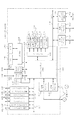
図13において、4はタイルスレーブインタフェースであり、タイル伸張部(1)2103からタイルバス2107を介してデータパケットを受け取るためのインタフェースである。5はメモリインタフェースであり、タイルスレーブインタフェース4が受け取ったタイルデータを外部メモリ上にラスタ展開し、後述する変倍ブロックが必要とするタイルデータをラスタ展開されたメモリから読み出してくるためのインタフェースである。6は変倍ブロックであり、実際に変倍操作を行う。7はタイルバッファであり、変倍処理されたタイルデータを1タイル分蓄積する。8はタイルマスターインタフェースであり、変倍処理されたタイルデータをタイル圧縮部(1)2108にタイルバス2107経由で出力する。9は変倍ブロック6で変倍率及びフィルタの設定等を行うためのレジスタインタフェースである。
【0127】
この変倍処理部2116においては、まずタイルスレーブインタフェース4にデータパケットが入力される。ここで、タイルスレーブインタフェース4は入力されたデータパケットのヘッダの内容を解析する。具体的には、データパケットのヘッダに含まれるPageID3007及びJobID3008を検出しデータの正当性を確認し、更に、PacketIDY3009及びPacketIDX3010にてパケットの画像全体における位置を把握する。このとき、タイル伸張部2103によってProcess Instruction3011は既に8ビットシフトされており、UnitID2及びMode2はそれぞれ、UnitID1及びMode1になっている。そして、メモリインタフェース5に対し位置情報とともにタイルデータを出力し、メモリインタフェース5は確保されている外部メモリ2123上にタイルデータを展開する。
【0128】
変倍ブロック6は、メモリインタフェース5を介して入力されたタイルデータに対して150%の画像伸張を行う。この詳細な処理については後述する。
【0129】
変倍処理されたタイルデータは順次、タイルバッファ7を介してタイルマスターインタフェース8に送られる。ここで、タイルマスターインタフェース8は、変倍ブロック6から送られてきたデータ長に関する情報に基づき、有効画素範囲情報(図3に示したデータパケットの、valid width3021及びvalid height3022)等をヘッダに記載する。具体的には、タイルマスターインタフェース8は、タイルデータに関して、validwidth3021及びvalid height3022にそれぞれ、有効画素範囲情報としての値“32”及び“32”を記述する。
【0130】
そして、タイルマスターインタフェース8は、各タイルデータと、それぞれのタイルデータに対応したヘッダとから新たにデータパケットを生成する。ここで、Process Instruction3011は8ビットシフトされ、UnitID1にタイル圧縮部(1)2106のIDが記載され、Mode1にはタイル圧縮部の処理を記述したMode2の値がシフトされる。同様に、UnitID2以降のUnitID及びModeも8ビットシフトが行われるが、今回の例では圧縮部での処理が最後であるため結果的には何も格納されない。
【0131】
次に、タイルマスターインタフェース8は、タイルバス2107に対してシフト後のUnitID1に該当するタイル圧縮部(1)2106への接続を要求する。その後、タイルマスターインタフェース8は、タイルバス2107によってタイル圧縮部(1)2106に接続されると、データパケットをタイル圧縮部(1)2106に転送する。
【0132】
タイル圧縮部(1)2106ではデータパケットをJPEG圧縮し、JPEG圧縮されたデータパケットを画像リングインタフェース2102に転送する。画像リングインタフェース2102は画像リング2008を介して、システム制御部2150に転送する。そして、最後にシステム制御部2150が、転送されてきたデータパケットのタイルデータをRAM2002に格納することによって、一連の変倍処理が終了する。
【0133】
[変倍処理の詳細]
ここで、変倍処理部2116における変倍ブロック6の変倍処理について更に詳述する。
【0134】
図14は、変倍ブロック6の詳細な構成を示すブロック図である。図14において、10は変倍コントロールブロックであり、変倍処理全体を制御する。11はバッファであり、メモリバス2108と変倍ブロック6間のタイルデータの幅及びスピード差を吸収する。12は水平変倍回路であり、水平方向の変倍処理を行う。13は水平方向の変倍処理結果を格納する複数のラインバッファであり、タイルの水平方向画素分の長さを持つ。14は垂直変倍回路であり、垂直方向の変倍処理を行う。
【0135】
図15は、外部メモリ2123上に展開されるタイル単位のラスタデータを示す図である。図15において、15は処理される画像全体を示す。16はタイルに分割された画像を示し、タイル内の番号は原画像におけるタイルの位置をxy座標で示している。17は外部メモリ2123に実際に確保されるメモリエリアであり、垂直方向1タイル分の処理が終了する毎に、このエリア17は図の下側へ移動する。
【0136】
図16は、図14に示した変倍コントロールブロック10の詳細を示すブロック図である。図16において、20はタイミング発生回路、21は水平アドレス保持回路、22は水平アドレスカウンタ、23は垂直アドレス保持回路、24は垂直アドレスカウンタ、25は水平変倍情報保持回路、26は垂直変倍情報保持回路である。
【0137】
まず、タイル伸張部(1)2103からタイルバス2107を介してタイルスレーブインタフェース4に入力されたタイルデータはメモリインタフェース5に転送され、メモリバス2108及びメモリ制御部2122を介して、一旦図15に示されるように1枚の画像の形に戻される。但し、外部メモリ2123は1枚の画像データ分を確保しているわけではなく、必要な垂直のメモリ確保量は変倍処理を行うのに必要とされる量、即ち、図15に示す太線で示されるエリアを展開できる程度の量が実際には確保される。更に、メモリインタフェース5は少なくとも垂直方向に1タイル分の画像データを外部メモリ2123に展開し終えた時点で変倍ブロック6にReady信号を通知する。
【0138】
一方、変倍ブロック6はメモリインタフェース5からReady信号を受けて変倍処理に必要なタイルデータのアドレスをメモリインタフェース5に通知し、外部メモリ2123からの読み出し要求を行う。読み出し要求を受けたメモリインタフェース5はメモリバス2108を介して外部メモリ2123から該当する位置のタイルデータを読み出して変倍ブロック6へ送出する。これにより、変倍ブロック6はメモリインタフェース5より送出されたタイルデータ及びレジスタインタフェース9を介して設定された変倍率及びフィルタ係数に基づき変倍処理を実行する。そして変倍ブロック6は、変倍処理を行った結果をタイルバッファ7に蓄積し、1タイル分の変倍画像を生成し終えた段階でタイルマスターインタフェース8にDone信号を通知する。このDone信号を通知されたタイルマスターインタフェース8は、変倍結果のタイルデータをタイルバッファ7より読み出し、タイルバス2107を介して次の処理ブロック(タイル圧縮部)へ出力を行う。
【0139】
このように、図13に示すメモリインタフェース5より送出されたタイルデータは図14に詳細を示す変倍ブロック6のバッファ11でバス幅の違い及び画像の読み出し速度の違いを吸収し、水平変倍回路12で水平方向の変倍操作を行う。この変倍処理を行う回路は前述した図15に示したフィルタ回路と同じである。そして、水平方向に変倍処理された結果はラインバッファ13に格納され、垂直変倍回路14で垂直方向の変倍処理が行われた後、図13に示すタイルバッファ7に出力される。
【0140】
ここで、図16を参照しながら上述の変倍コントロールブロック10の詳細な構成及び動作について説明する。
【0141】
図1に示すメモリインタフェース5からDone信号を受けて、変倍コントロールブロック10のタイミング発生回路20は、バッファ11及び水平変倍回路12(図14)、図16に示す水平アドレスカウンタ22の各ブロックにLineStart信号を出力する。また、タイミング発生回路20は、ラインバッファ13及び垂直変倍回路14(図14)、図16に示す垂直アドレスカウンタ24の各ブロックにTileStart信号を出力する。さらに、タイミング発生回路20は、図16に示す水平アドレス保持回路21及び水平変倍情報保持回路25にXstart信号を出力し、垂直アドレス保持回路23及び垂直変倍情報保持回路26にYstart信号を出力して各ブロックを初期化させる。その後、メモリインタフェース5へタイルデータの読み出し要求信号Reqを出力する。また、水平アドレスカウンタ22及び垂直アドレスカウンタ24は、変倍処理を行うのに必要な読み出したいタイルデータのアドレスを示す信号Addressを出力する。
【0142】
ここで、外部メモリ2123よりタイルデータが読み出され、従来例と同様な水平方向の変倍処理がタイル単位で開始され、水平方向アドレスカウンタ22は原画像データのシフトが発生したことを示すHshift信号に基づき、カウンタの値をカウントアップしていく。
【0143】
その後、タイル1ライン分の水平方向変倍処理が終了すると(HDone信号)、タイミング発生回路20は新たにバッファ11及び水平変倍回路12(図14)、図16に示す水平アドレスカウンタ22、垂直アドレスカウンタ24の各ブロックにLineStart信号を出力し、バッファ11及び水平変倍回路12を初期化する。これと同時に、図16に示す水平アドレスカウンタ22のカウント値を水平アドレス保持回路21にロードし、フィルタ係数生成回路には水平変倍情報保持回路に保持された値(RegHInf)をロードさせ、垂直アドレスカウンタ24の値をカウントアップさせる。そして、更新された水平及び垂直アドレスAddressと読み出し要求信号Reqとに基づき、メモリインタフェース5は次のラインの画像データを外部メモリ2123から読み出す。
【0144】
上述の操作により、図14に示すラインバッファ13に所定の変倍結果が揃うと垂直方向変倍回路14が動作を開始し、タイルのライン数分の変倍処理を終了するとタイル終了信号Vdone信号が図16に示すタイミング発生回路20に入力される。この信号に基づきタイミング発生回路20は水平アドレス保持回路21に次の水平アドレスカウンタの値を保持させる信号TileDoneを出力する。これらの処理を繰り返した後、変倍出力タイルが水平方向の最後のタイルを処理し終えたときにタイミング発生回路20は垂直アドレス保持回路23に対し、現在の垂直アドレスカウンタ24の値を保持させる信号Xlastを出力する。これにより、タイミング発生回路20は垂直アドレス保持回路23に現在の垂直アドレスカウンタ値を保持させる。
【0145】
次の出力タイルは水平方向アドレスが0であるので、タイミング発生回路20はTileStart信号を出力する前に水平アドレス保持回路21の値を初期化する信号Xstart信号を水平アドレス保持回路21に出力する。そして、水平アドレス保持回路21により保持されている水平アドレスが初期化された後、出力基準にて垂直方向に1タイル進んだタイルの変倍処理が実行される。ここで、ラインバッファ13は、変倍処理部2116の出力がタイル基準で実行されるため、1タイル画像の水平方向画素数分の長さを持つ複数の(先の従来例と同様であれば8ライン分)ラインバッファで構成される。したがって、1タイルの水平方向画素数がもし32画素であるとすれば先の従来例に比べおおよそ200分の1の量でよいことになる。
【0146】
以上説明したように、本実施形態によれば、必要とするラインバッファの長さはタイルの水平方向画素数分であり、垂直方向の変倍フィルタの構成を従来例と同様とすると、1タイルの水平方向画素数を32、処理できる最大画素の水平方向画素数を約7000画素とした場合、変倍処理部2116が必要とするラインバッファの量は従来例のおおよそ200分の1で済む。したがって、少ないラインバッファの量で従来例の変倍装置と同等な変倍処理が可能であり、変倍処理を含む複数の機能を1つのICチップ内に実現するのに最適である。
【0147】
また、タイル画像のラスタ展開用のメモリを外部メモリとしているため、様々な変倍率やより大きな画像サイズへの対応を考えた場合にもタイルのサイズが同じであるならばICチップ内の回路規模にはほとんど影響がなく対応が可能である。
【0148】
また、変倍処理部は、CPU等から直接制御されることなく、データパケットのヘッダの座標情報に基づいて外部メモリ上の適切な領域に画像データをラスタ展開することができるので、外部メモリを用いた変倍処理におけるデータの管理が容易である。
【0149】
(第2の実施形態)
第1の実施形態のような装置構成であっても、画像データがフルカラーである場合等においては、かなりの大きさの外部メモリが要求されることがある。例えばA4長手サイズ、600dpiの画像では約7000画素となり、1タイルの垂直方向画素数を32とすると、8ビットフルカラーの画像データを1タイル幅でラスタ展開するには、おおよそ1Mバイトの外部メモリが必要とされる。さらに、変倍処理として、特に垂直方向の縮小を行うためには複数のタイルが必要とされるため、ラスタ展開に必要とされるメモリ量は更に増大する。
【0150】
このような状況を考慮した場合、外部メモリに、レイテンシーの高いSRAMを用いるより、汎用のSDRAMを用いるほうがコスト的には好ましい。
【0151】
しかしながら、変倍回路においては変倍率によって変倍処理に必要な開始画素位置も必要とされる画素数も異なってくる。このため、画像メモリにSDRAMを用いた場合、必要な画素データ全てを1度にバースト転送することは処理上も、またバッファの量的にも問題があり、どうしてもメモリからの画素データの読み出し待ち時間により変換処理速度が上がらなくなってしまう。
【0152】
本実施形態では、変倍処理の開始時に、外部のメモリにラスタ展開された画像データの読み出しデータ量を制御することにより、例えばSDRAMのように読み出し待ち時間が生じる画像メモリを用いた場合でも、高速な変倍処理を実行可能とする。
【0153】
[変倍処理の詳細]
本実施形態の変倍処理部2116のブロック構成は、図13に示したものと同じである。図17は、図13に示したメモリインタフェース5の詳細な構成を示す図である。
【0154】
図17において、501は書き込み制御回路であり、図13に示したタイルスレーブインタフェース4からのデータを受け取り、外部メモリ2123への書き込み制御を行う。502は読み出し制御回路であり、図13に示した変倍ブロック6からの要求信号を受け取り、必要な画像データを外部メモリ2123から読み出す。503はメモリインタフェース制御回路であり、書き込み制御回路501及び読み出し制御回路502からの要求に応じて外部メモリ2123との通信を行い、データの書き込み又は読み出しを制御する。
【0155】
図18は、図17に示した読み出し制御回路502の詳細な構成を示す図である。図18において、601はリクエストカウンタ(ReqCount)であり、外部メモリの読み出しリクエスト数をカウントする。602はリードリクエスト生成回路(RReqGen)であり、変倍ブロック6のバッファ(FIFO)状態を示す信号(NotFull)や水平方向変倍開始パルス(LineStart)又は変倍に必要なデータの位置を示すメモリアドレス(Address)を受け取り、メモリ読み出し信号(Req)と読み出しアドレス(RAddr)を生成する。603はリードカウンタ(ReadCount)であり、読み出し要求から求められるデータ数と実際に読み出されたデータ数をカウントする。604はOR回路であり、リクエストカウンタ601から出力されるStartDone信号とリードカウンタ603から出力されるCountZero信号とを入力し、その論理和を出力する。605はAND回路であり、リードリクエスト生成回路602から出力されるReq信号とOR回路604から出力される信号とを入力し、その論理積を出力する。
【0156】
以上の構成を有する変倍回路の動作について図中に示す信号を参照しながら説明する。
【0157】
タイル伸張部(1)2103から、図13に示したタイルバス2107を経由してタイルスレーブインタフェース4に入力された画像データは、メモリインタフェース5に転送され、メモリバス2108及び外部メモリインタフェース2122を経由して、一旦図15に示した、1枚の画像の形に戻される。
【0158】
第1の実施形態と同様に、外部メモリ2123は1枚の画像データ分を確保しているわけではなく、必要な垂直のメモリ確保量は変倍処理を行うのに必要とされる量、即ち、図15に示した太線のエリアを展開できる程度の量が実際には確保される。更に、図1に示したメモリインタフェース5は、少なくとも垂直方向に1タイル分の画像データを外部メモリ2123に展開し終えた時点で変倍ブロック6にReady信号を通知する。
【0159】
一方、変倍ブロック6はメモリインタフェース5からのReady信号を受けて変倍処理に必要な画像データのアドレスをメモリインタフェース5に通知し、読み出し要求を行う。読み出し要求を受けたメモリインタフェース5はメモリバス2108経由で外部メモリ2123から該当する位置の画像データを読み出して変倍ブロック6へ送出する。これにより、変倍ブロック6はメモリインタフェース5より送出された画像データ及びレジスタインタフェース9を介して設定された変倍率及びフィルタ係数に基づき、変倍処理を行う。そして、その結果をタイルバッファ7に蓄積し、1タイル分の変倍画像を生成し終えた段階で、タイルマスターインタフェース8にDone信号を通知する。Done信号を通知されたタイルマスターインタフェース8は、変倍結果の画像をタイルバッファ7より読み出し、タイルバス2107を介してタイル圧縮部(1)2106へ出力する。
【0160】
ここで、メモリインタフェース5で授受される信号は図17に示したようになる。そして、図13に示したタイルスレーブインタフェース4より得られた画像データ(TsData)とタイルの番号(Tpos)が書き込み制御回路501で対応する外部メモリのアドレスに書き込むようにメモリインタフェース制御回路503に対して書き込みリクエスト信号(WReq)を出力する。そして、最終的に対応するメモリのアドレスへ画像データが書き込まれる。
【0161】
一方、外部メモリ2123に書き込まれた画像データのうち、変倍ブロック6にて変倍処理に必要とされる画像データは、読み出し制御回路502において、変倍ブロック6より得られる水平方向変倍開始パルス(LineStart)と、それ以前に確定された読み出し開始アドレス(SAddress)と、変倍ブロック406のバッファ状態を示す信号(NotFull)とに基づき、読み出され始める。ここで、読み出し制御回路502で授受される信号は図17に示したようになる。
【0162】
次に、この読み出し制御回路502の動作を図19に示すタイミングチャートを参照しながら説明する。まず、変倍ブロック6からの水平方向変倍開始信号(LineStart)パルスが“1”にアサートされる(t0)。この時、図18に示したリードリクエスト生成回路(RReqGen)602からの読み出しアドレス(RAddr)が変倍ブロック6に供給される読み出し開始アドレス(SAddress)としてラッチされる。そして、メモリ読み出し信号(Req)により変倍ブロック6のバッファ状態を示す信号(NotFull)のサンプリングが開始される。
【0163】
同時に、リクエストの発行数をカウントするリクエストカウンタ(ReqCount)601の発行カウンタを“0”にリセットし、StartDone信号を“1”にセットする。StartDone信号によりAND回路605によるマスクを解除されたReq信号はRReq信号として図17に示すメモリインタフェース制御回路503に読み出し要求を通知する。これに応じて、メモリインタフェース制御回路503が外部メモリインタフェース2122と通信を行い、読み出し要求受理信号を受けると、RAck信号は“1”にセットされる。
【0164】
このRAck信号が“1”にアサートされたことを確認すると(t1)、リクエストカウンタ(ReqCount)601の発行カウンタを1増加し、リードリクエスト生成回路(RReqGen)602は読み出しアドレス(RAddr)の値を必要なだけインクリメントする(この例では8)。同時に、リードカウンタ(ReadCount)603が読み出し要求のビート数だけ、カウンタの値を増加させる。尚、カウンタの値が“0”でなくなったため、CounZero信号は“0”になるが、リクエストカウンタ(ReqCount)601から出力されるStartDone信号が“1”であるため、OR回路604の出力は“1”でありつづける。従って読み出し要求信号RReqは“1”でありつづける。
【0165】
次に、外部メモリインタフェース2122への読み出し要求を終えたメモリインタフェース405は新たな読み出し要求信号(RReq)に基づき新たな読み出し要求を外部メモリインタフェース2122に発行したことをRAck信号で通知する。RAck信号で読み出し要求が伝わったことを検知すると、リクエストカウンタ(ReqCount)601、リードリクエスト生成回路(RReqGen)602からの読み出しアドレス(RAddr)、及びリードカウンタ(ReadCount)を上述のt1と同様にそれぞれ必要な値だけ増加させる(t2)。尚、図19に示す例では、カウンタ及びアドレスの値は16進表記である。
【0166】
その後、外部メモリインタフェース2122より画像データの読み出し準備が整い、読み出しが開始されたことを示す信号(RdValid)が“1”にアサートされると、リードカウンタ(ReadCount)603はそのカウンタの値を現在値から“1”づつ減少させる(t3)。変倍ブロック406のバッファ(FIFO)にまだ余裕があり、読み出し要求(RReq)が“1”であったため、メモリインタフェース405経由で外部メモリ2123に要求していた読み出し要求が受け付けられたことを示すRAck信号が帰ってくる。そして、先ほど(t2)と同様に、リクエストカウンタ(ReqCount)、読み出しアドレス(RAddr)が必要な値だけ増加される。
【0167】
但し、現時点で既にデータの読み出しが開始されているため、リードカウンタ(ReadCount)603の値は、通常の増加分(この例では“8”)を増加させた値から読み出しによる減少分“1”があるため、直前の値より結果的に“7”だけ増加した値となる(t4)。
【0168】
変倍ブロック6のバッファ(FIFO)にまだ余裕があり、読み出し要巨M号(RReq)が“1”であったため、メモリインタフェース2122経由で外部メモリ2123に要求していた読み出し要求が受け付けられたことを示すRAck信号が帰ってくる。そして、読み出しアドレス(RAddr)が必要な値だけ増加され、リードカウンタ(ReadCount)603も先ほどと同様に直前の値に対して“7”だけ増加する。
【0169】
一方、リクエストカウンタ(ReqCount)601は今回の読み出し要求の受付でバッファ(FIFO)の段数分の読み出しを終了するので現時点の値を保持し、StartDone信号が“0”にデアサートされる。これにより、変倍ブロック406のバッファ(FIFO)状態を示す信号(NotFull)の状態にかかわらずマスク用の信号StartDone及びCountZeroの両信号が共に“0”となる。従ってOR回路604の出力は“0”、AND回路605の出力も“0”となり、メモリインタフェース2122への読み出し要求信号は発生しなくなる(t5)。
【0170】
ここで、外部メモリ2123から順調に画像データの読み出しが行われ、読み出し要求分の画像データの読み出しが終了すると、リードカウンタ(ReadCount)603は“0”となり、CountZero信号は“1”となる。これにより、読み出し要求信号(RReq)のマスクが解除され、新たな読み出し要求信号がメモリインタフェースに対して発行される(t6)。
【0171】
本実施形態では変倍ブロック406が順調に画像データ処理を行い、結果的にバッファが一杯にならなかった場合を示している。もちろん、変倍率の設定で画像データの消費量が異なり、バッファが一杯に近い状態になり、バッファ状態を示す信号(NotFull)が“0”となる場合もありうる。この場合には、もちろん読み出し要求は発生しない。
【0172】
その後、外部メモリインタフェース2122に読み出し要求が受け付けられ、RAckが帰ってくるとリードカウンタ(ReadCount)603はビート数“8”だけ増加する。そして、CountZero信号は“0”となり、Req信号のマスクが有効になり、読み出し要求信号(RReq)は“0”となり、新たな読み出し要求は、(t7)で受け付けられた読み出し要求が完了するまで発行されない。
【0173】
以上説明したように、本実施形態によれば、各タイルに関して、水平方向の変倍処理開始時に水平変倍回路のバッファの量だけの画像データを変倍処理回路の処理状態によらず、メモリインタフェースから転送するようにした。これにより、水平変倍回路が処理を行う際に必要な画像データがメモリインタフェースからの読み出し待ち状態となることを少なくでき、処理速度の高速化が可能となる。
【0174】
また、読み出し処理を集中させることにより外部SDRAMのヒット率を高くすることができ、ICチップ内の外部SDRAMを用いる機能ブロックに対しても、ラスタ展開時の書き込みについても高速化が図れる。
【0175】
更に、変倍処理のように処理の開始時点で必要とされるデータ量すべての読み出しが困難であり、逐次的に読み出さざるを得ないシステムにおけるスプリットトランザクションをサポートする読み出し制御を簡単に行える。
【0176】
以上、外部SDRAMを用いる変倍処理部を例に説明したが、変倍処理部に限らず、他の処理ブロックにおける画像処理にも、本実施形態における発明を適用することができる。
【0177】
例えば、図9の画像入力処理におけるタイル画像の生成処理の際に、画像入力インタフェース2112において、タイル単位でのラスタ展開のために画像メモリを用いている。このとき、本実施形態と同様な連続読み出しのメモリアクセス制御を行うことができ、タイル画像生成の高速化が達成できる。
【0178】
(第3の実施形態)
上記実施形態のように、外部メモリを用いて変倍処理を実行する場合、メモリを管理して処理の信頼性を向上させるために、外部メモリへのタイル画像の書き込み、読み出しに対する排他制御を行うことが好ましい。本実施形態では、以下説明するような排他制御の構成をとることにより、変倍率に応じたメモリ管理を、簡単な装置構成で実行できるようにする。
【0179】
[変倍処理の詳細]
本実施形態の変倍処理部2116のブロック構成は、図13に示したものと同じである。図20は、図13に示したメモリインタフェース5の一例を示す詳細ブロック図である。
【0180】
図20において、書き込み制御回路501、読み出し制御回路502、メモリインタフェース制御回路503は、第2の実施系形態で説明した同一符号の回路と同様な機能を有している。
【0181】
701は排他制御回路で、書き込みを行おうとしているタイルの位置情報(タイルポジション信号Tpos)と、読み出しを行おうとしている読み出しアドレスに基づき書き込み、読み出しの許可(許可信号TREnable)を与える制御を各信号Tpos,TWEnable,TileStart,SAddressに従って行う。
【0182】
図21は、図20に示した排他制御回路701の詳細回路の一例を示すブロック図である。
【0183】
図21において、801はExclusiveORゲート、802はD−FlipFlop、803はEnable付きのD−FlipFlop、804はデコーダ回路、805−1−s0〜805−1−s7,805−2−m0〜805−2−m7はAnd回路、806−1〜806−8はRS−FlipFlop、807はマスク生成回路(MaskGen)、808はアンドゲートである。
【0184】
図22〜図25は、図20に示した排他制御回路701によるタイル画像データ転送処理時のメモリ状態を説明するための図である。
【0185】
図22〜図25において、tFlag0〜7は変倍処理の進行状態に従い変化する同一垂直方向のタイル位置の変倍処理終了有無を示すフラグで、ラスタ展開される外部のメモリ上の垂直方向のタイル位置に応じたメモリ状態がRS−FlipFlop806−1〜806−8上に保持される。
【0186】
なお、RS−FlipFlop806−1〜806−8は、図21に示した排他制御回路701のデコード回路804の出力とマスク回路807の出力とに基づいてセット(「1」)またはリセット(「0」)される。そして、該フラグtFlag0〜7の状態に従って、外部のメモリに対するデータ書き込み時におけるタイルスレーブインタフェース4によるデータの受信動作、すなわちタイルスレーブインタフェース4に対する信号TWEnableのセットまたはリセットを制御するとともに、外部のメモリからのデータ読み出し時における読み出し制御回路502に対する信号TREnableのセットまたはリセットを制御する。
【0187】
なお、本実施形態においては、図22〜図25において変倍装置で変倍可能な最小倍率は、例えば0.25(1/4)であるとし、ラスタメモリの垂直方向のタイル数は条件式より求められる最小の値(4+2=6)であるから、これ以上、かつ最小の2のべき乗の値である「8」として説明する。
【0188】
変倍動作開始時には、図22〜図25におけるフラグtFlag0〜7はすべて「0」にクリアされた状態にあり、画像データはタイルバスにて図22中の左上から順に送られてくる。
【0189】
図22に示す例では、一番上の左から3つ目までがデータ転送が終了し、現在4つ目の図22の斜線で示されたタイル画像の転送が現在行われているとする。
【0190】
そして、タイル画像の転送がさらに進み、図22の一番上の列の転送が終了し、図23に示すように上から2列目の転送が開始されると、1列目の書き込み終了を示すフラグtFlag0が「1」にセットされる。同様にして列の書き込みが終了した時点で該当するフラグが順次「1」にセットされる。
【0191】
一方、変倍処理による読み出し側の制御は、例えば、1/4倍の変倍を行っている場合のメモリ状態は図24に示す通りであり、図24ではラスタ展開された画像のうち斜線で示された(3,8n)から(8,8n+5)のタイルに含まれる画像データを用い、1タイル分の変倍結果を出力しようとしている。
【0192】
本来、変倍率が(この例では水平垂直とも)1/4であるので、水平方向および垂直方向とも、4タイルずつ(この例では(4,8n+1)から(7,8n+4)の部分)の画像があればよいと思われるが、実際にはフィルタ処理を行う関係上周辺の画像データをも必要とするため、図24に示すような(3,8n)から(8,8n+5)のタイルに含まれる画像データが必要となる。
【0193】
この状態から水平方向に変倍処理を実行していき、水平方向の変倍処理を終え、垂直方向に変倍結果として1タイル分処理した場合のメモリの状態図およびフラグの値は図25に示す通りとなる。
【0194】
図25に示したように、つまり図24のメモリ状態から図25のメモリ状態に移った場合、変倍処理のために使用するタイル画像の位置は(0,8n+4)から(4,8(n+1)+1)の位置に移動する。ただし、(0,8(n+1))から(4,8(n+1)+1)の位置のタイル画像はメモリ上の位置は図24のタイル画像と同じであるが、新たにタイルスレーブより得られた画像データをおく必要があるため、該当するフラグtFlag0〜3は図示してあるようにクリアされている。
【0195】
これら図22から図23および図24から図25の変化に対応し該当するフラグのセットおよびクリアを実現する回路の一例が図21に示す排他制御回路701である。
【0196】
1垂直方向の画像データ書き込み終了時、つまり図22に示すメモリ状態から図23に示すメモリ状態への変化時には、タイルスレーブインタフェース4より入力されるタイルの位置を示す情報(信号Tpos)内の垂直方向情報(図20に示す信号Tpos(V))が変化する。したがって、その変化のタイミングを捉え、デコーダ回路24が出力する現在書き込み中の位置信号を、ゲートし、該当する位置のフラグをセットする信号(図22および図23の例ではゲート805−1−s0)を806のRS−FlipFlop806−1に出力する。該当するRS−FlipFlopはそのフラグをセットする。
【0197】
一方、1垂直方向分の変倍処理が終了した場合、つまり、図23に示すメモリ状態から図24に示すメモリ状態への変化時には、メモリからの水平位置の読み出しアドレスは「0」である。したがって、水平読み出しアドレスが「0」であるときのタイル変倍開始パルス(信号TileStart)でマスク生成回路27の出力を有効にしてやることでフラグをクリアする。
【0198】
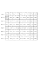
また、マスク生成回路807は、図23に示すメモリ状態時点での変倍開始時の垂直方向データ読み出しアドレスと、図24に示すメモリ状態時点での変倍開始時の垂直方向データ読み出しアドレスから読み出しが終了した垂直方向タイル位置を判断する。そして、判断結果から、読み出し終了位置に該当するフラグをクリアするための信号を発生する。デコーダ回路804の出力例を表1に示す。
【0199】
【表1】

このフラグデータに基づき、書き込み時には書き込もうとするタイル位置の画像データがすでに変倍処理による読み出しが終了しているかどうかを判断する。変倍処理による読み出しが終了していれば、図10に示された信号TWEnableを「1」にすることで、タイルスレーブインタフェース4はデータの受信を行う。逆に、変倍処理による読み出しが終了していない場合には、TWEnable信号を「0」にすることでタイルスレーブインタフェース4は本変倍装置に画像データを送ろうとしているタイルマスタインタフェース8を該当する位置の書き込みフラグが「0」になるまで待たせる。
【0201】
一方、読み出し時には、読み出そうとしているアドレスのフラグがセットされている場合には、図20に示した排他制御回路701から読み出し制御回路502に出力されるTREnable信号を「1」とし、図20の読み出し制御回路502はメモリインタフェース制御回路12に対しメモリ読み出し要求信号RReqおよびRAddr信号を出力する。
【0202】
逆に、フラグがセットされていない場合には、TREnable信号を「0」とすることで、読み出し制御回路502はメモリインタフェース制御回路503への読み出し要求信号の出力を制限する。
【0203】
上記実施形態では、書き込みのための制御信号TWEnableをタイルスレーブインタフェースに出力し、タイルデータの転送を制限したが、この信号を書き込み制御回路501へ出力し、書き込み要求信号を制限しても結果は同じである。
【0204】
本実施形態によれば、タイル画像をラスタ変換するためのメモリの書き込み、読み出しの排他制御を垂直方向のタイル単位で行い、しかも、管理すべき垂直方向のタイル数を変倍処理部が処理可能な最小倍率をn(<1)とした場合、管理すべき垂直方向のタイル数を(1/n)+2以上、かつ2のべき乗に制限することでメモリ管理を簡単に実現した。
【0205】
また、変倍処理部の特殊事情による読み出し済みメモリの解放に関しても垂直方向の出力タイルの変化時点に行うことで全体の構成を簡単に実現することが可能となった。
【0206】
なお、管理すべき垂直方向のタイル数は、2のべき乗に限定するものではない。すなわち、上記実施形態の構成において、垂直方向のタイル数を6、または7個としても、同様にメモリ管理を簡単にすることができる。
【0207】
(第4の実施形態)
上記各実施形態で説明した装置をICチップ化する場合、ある程度高速な変倍処理を実行することができるが、今後、さらなる変倍処理の高速化が要求されることが予想される。
【0208】
回路全体のクロック速度を上げることにより、この要求を満たす回路を構成することができるが、IC化に際する制約を与えことになる。また、外部メモリの要求スピードもクロック速度の高速化に伴い高速化されるため、使用されるメモリーチップのコストを上げる要因ともなる。
【0209】
本実施形態では、変倍処理回路に多少の回路を追加する代わりに、従来と同様なクロックスピードで従来よりも高速に変倍処理を行えるようにする。
【0210】
[変倍処理の詳細]
本実施形態における変倍処理部2116のブロック図を図26に示す。第1−3の実施系形態と異なるのは、タイルバッファ7を制御するためのタイルバッファ制御回路2601を設けた点である。
【0211】
本実施形態における変倍ブロック6の詳細な構成は、図14に示したものと同じであり、変倍コントロールブロック10の詳細な構成も、図16に示したものと同じである。
【0212】
ただし、変倍処理部2116は、上記各実施形態とは異なり、2タイル単位で変倍処理を実行する。以下、変倍処理部2116の全体動作を説明する。
【0213】
まず、タイル伸張部(1)2103から図26に示すタイルバス2107を介してタイルスレーブインタフェース4に入力されたタイルデータはメモリインタフェース5に転送され、メモリバス2108及びメモリ制御部2122を介して、一旦図11に示されるように1枚の画像の形に戻される。但し、外部の画像メモリ2123は1枚の画像データ分を確保しているわけではなく、必要な垂直のメモリ確保量は変倍処理を行うのに必要とされる量、即ち、上記実施形態と同様に、図15に示す太線で示されるエリアを展開できる程度の量が実際には確保される。更に、図26に示すメモリインタフェース5は少なくとも垂直方向に1タイル分の画像データを画像メモリ2123に展開し終えた時点で変倍ブロック6にReady信号を通知する。
【0214】
一方、変倍ブロック6はメモリインタフェース5からReady信号を受けて変倍処理に必要なタイルデータのアドレスをメモリインタフェース5に通知する。これを受けて、メモリインタフェース5は画像メモリ2123からの読み出し要求を行う。読み出し要求を受けたメモリインタフェース5はメモリバス2108を介して画像メモリ2123から該当する位置のタイルデータを読み出して変倍ブロック6へ送出する。これにより、変倍ブロック6はメモリインタフェース5より送出されたタイルデータ及びレジスタインタフェース9を介して設定された変倍率及びフィルタ係数に基づき、変倍処理を行った結果をタイルバッファ7に蓄積し、2タイル分の変倍画像を生成し終えた段階でタイルマスターインタフェース8にDone信号を通知する。このDone信号を通知されたタイルマスターインタフェース8は、変倍結果のタイルデータをタイルバッファ7よりタイル単位で読み出し、タイルバス2107を介してタイル圧縮部(1)2106へ出力を行う。
【0215】
ここで、図16を参照しながら上述の変倍コントロールブロック10の詳細な構成及び動作について説明する。
【0216】
図26に示すメモリインタフェース5からDone信号を受けて、変倍コントロールブロック10のタイミング発生回路20は、バッファ11及び水平変倍回路12(図14)、図16に示す水平アドレスカウンタ22の各ブロックにLineStart信号を出力する。また、タイミング発生回路20は、ラインバッファ13及び垂直変倍回路14(図14)、図16に示す垂直アドレスカウンタ24の各ブロックにTileStart信号を出力する。さらに、タイミング発生回路20は、図16に示す水平アドレス保持回路21及び水平変倍情報保持回路25にXstart信号を出力し、垂直アドレス保持回路23及び垂直変倍情報保持回路26にYstart信号を出力して各ブロックを初期化させる。その後、メモリインタフェース5へタイルデータの読み出し要求信号Reqを出力する。また、水平アドレスカウンタ22及び垂直アドレスカウンタ24は、変倍処理を行うのに必要な読み出したいタイルデータのアドレスを示す信号Addressを出力する。
【0217】
ここで、外部メモリ2123よりタイルデータが読み出され、水平方向の変倍処理が開始され、水平方向アドレスカウンタ22は元画像データのシフトが発生したことを示すHshift信号に基づき、カウンタの値をカウントアップしていく。
【0218】
その後、タイル1ライン分の2倍の画素数分の水平方向変倍処理が終了すると(HDone信号)、タイミング発生回路20は新たにバッファ11及び水平変倍回路12(図14)、図16に示す水平アドレスカウンタ22、垂直アドレスカウンタ24の各ブロックにLineStart信号を出力し、バッファ11及び水平変倍回路12を初期化する。これと同時に、図16に示す水平アドレスカウンタ22のカウント値を水平アドレス保持回路21にロードし、フィルタ係数生成回路には水平変倍情報保持回路に保持された値(RegHInf)をロードさせ、垂直アドレスカウンタ24の値をカウントアップさせる。そして、更新された水平及び垂直アドレスAddressと読み出し要求信号Reqとに基づき、メモリインタフェース5は次のラインの画像データを外部メモリ2123から読み出す。
【0219】
上述の操作により、図14に示すラインバッファ13に所定の変倍結果が揃うと垂直方向変倍回路14が動作を開始し、垂直方向に変倍処理を実施した結果画像データをタイルバッファ制御回路2601に出力する。垂直方向変倍回路14においてタイルのライン数分の変倍処理を終了するとタイル終了信号Vdone信号が図16に示すタイミング発生回路20に入力される。この信号に基づきタイミング発生回路20は水平アドレス保持回路21に次の水平アドレスカウンタの値を保持させる信号TileDoneを出力する。これらの処理を繰り返した後、変倍出力タイルが水平方向の最後のタイルを処理し終えたときにタイミング発生回路20は垂直アドレス保持回路23に対し、現在の垂直アドレスカウンタ24の値を保持させる信号Xlastを出力し、垂直アドレス保持回路23に現在の垂直アドレスカウンタ値を保持させる。
【0220】
一方、タイルバッファ制御回路2601は垂直方向変倍回路14にて垂直方向の変倍をも実施された変倍結果画像データを数え、タイルバッファの該当する位置へと書き込みを行う。また、タイルマスターインタフェース回路の読み出し要求アドレスに従い該当するタイル画像データを読み出し、出力する。このとき、読み出すべきタイル画像データが水平方向に連続した2つのタイル画像のうち初めのものであるか後のものであるかを判断し、読み出しアドレスを該当するアドレスに変換してタイルバッファから読み出しを行う。
【0221】
タイルバッファ制御回路2601の一例を図27に示す。図27において、2701は変倍ブロック6より変倍結果画像と同時に出力されるValid信号をカウントする書き込みアドレスカウンタ、2702はタイルマスターインタフェースより読み出し要求を受けて読み出し画素数をカウントする読み出しアドレスカウンタである。
【0222】
本実施形態の変倍処理の特徴を明確に説明するため、タイルの大きさを水平方向8画素、垂直方向8ラインであるとする。この場合のタイルバッファ7におけるアドレスの一例を図28に示す。図28にてハッチがかかっている部分が最初のタイル部分を示す。
【0223】
タイルバッファ7への書き込み時は、書き込みアドレスは図28に示した番号順に出力され、タイルバッファ上の図示される位置に格納される。一方、読み出し時にはタイル単位で出力する必要があるため、読み出しアドレスを0→1→…→7→16→17→…として読み出し、図にてハッチがかかった部分を読み出した後、今度は8→9→…→15→24→…と読み出しを行う。そのため、読み出しアドレスは読み出しアドレスカウンタの出力アドレス信号の位置を入れ替えた信号をタイルバッファ7に与えることで実現できる。
【0224】
次に、本実施形態の構成を用いて変倍処理を行った場合のタイル1ラインあたりの処理時間を概算する。まず、タイル単位で処理を行う場合と、水平方向に2タイル連続して処理を行う場合との処理領域の違いを図29に示す。図29は簡単のため変倍率を1(つまり100%)とした時の処理に必要な原画像データと、出力のタイルを示すものである。図29(a)はタイル単位で処理を行う場合を図示し、ハッチがけを行った部分が外部メモリから読み出す必要がある画像データである。図に示すように、タイル単位で処理を行うため中央の濃い色でハッチがけされた部分は実際には外部メモリから2回、(最初のタイルの最後と次のタイルの最初)読み出される必要がある。
【0225】
2タイル連続して出力を行う本実施形態の処理結果を図29(b)に図示する。図29(b)では、水平方向に連続した2タイルを一度に処理するため、図29(a)で示したような外部メモリ2123から2度読み出さなければならない領域が発生していない。もちろん、2タイル連続したタイルを生成した後には、同じように2度読みする領域が発生するが、その発生頻度は図29(a)に図示した場合の半分である。
【0226】
次に、倍率1の場合のラインあたりの処理に要するクロックサイクルの概算を行う。処理を開始し、メモリインタフェースから画像データが出力されるまでの遅延は外部メモリを用いる以上避けることができず、読み出し要求を出してから、実際にメモリからデータが読み出されるまでのサイクル数は水平変倍回路が動作できない不要なサイクルとなる。このサイクル数をTAとする。
【0227】
また、メモリからの読み出しは、高速アクセスを行う必要上、バースト読み出しを行う必要があり、読み出し開始位置と、実際に変倍処理に必要な画素位置とが一致するとは限らないため、ここでも不要なサイクルが発生し、その値をTBとする。
【0228】
変倍演算開始時のオーバーヘッドおよび、パイプライン処理終了処理に要するサイクル数をTCとする。
【0229】
以上の条件にて実際の水平方向処理サイクル数を計算する、ただし、上記TA、TB、TCには各々10、7、5を代表値として用いるとすると、1タイル相当画素数の水平変倍に要する処理サイクルは
TA+TB+32+TC=54
一方、連続した2タイル分の水平方向変倍を一括処理する場合には
TA+TB+64+TC=86
これを1タイル分に換算するとその半分になるので86/2=43
となり、平均して約20%の処理サイクルの短縮つまり、高速化が可能となる。
【0230】
以上説明したように、本実施形態では、2つのタイルを処理するので、クロック速度の高速化等を行わなくても、高速な変倍処理が可能となる。なお、一括して処理するタイルの数は2つに限るものではなく、3つや4つを一括して処理するようにしてもよい。
【0231】
(第5の実施形態)
上記第4の実施形態では、複数タイルを一括して変倍処理するため、水平方向の端部の処理時には、本来必要としないデータまでも変倍ブロックから出力されてしまうことがある。
【0232】
本実施形態では、複数タイル単位で変倍処理する場合においても、有効なタイルのみを出力するように変倍処理部を制御する。
【0233】
[変倍処理の詳細]
本実施形態における変倍処理部2116のブロック構成は、第4の実施形態で説明した図26のものと同様である。ただし、タイルバッファ制御回路2601の構成が、第4の実施形態と異なっている。以下、タイルバッファ制御回路2601の詳細について説明する。
【0234】
本実施形態のタイルバッファ制御回路のブロック図を、図30に示す。図30において、3001は変倍ブロック6より変倍結果画像と同時に出力されるValid信号をカウントする書き込みアドレスカウンタ、3002はタイルマスタインタフェースより読み出し要求を受けて読み出し画素数をカウントする読み出しアドレスカウンタである。
【0235】
図31はタイルバッファのアドレス配置を説明するための図である。いま、図31(a)に示されるように、タイルバッファが水平方向に2タイル分領域を確保して用いられているとすると、書き込み時のアドレスは図中に示されるようなアドレス配置となり、下位6ビットは水平方向の画素カウンタで占められ、上位5ビットはライン方向のカウンタで占められる。
【0236】
一方、図31(b)に示されるように、タイルバッファに格納されたタイルデータの読み出し時のアドレスは、タイル単位で読み出す必要上、水平方向に偶数番目のタイルか奇数番目のタイルかを示すビットがはさまれ、それより下位側の5ビットはタイル内の水平方向画素アドレスを、上位側5ビットは垂直方向のラインアドレスで占められる。
【0237】
この読み出し時のアドレスを正しく生成するために、読み出しアドレスカウンタは図32にて示されるようなフローに従いアドレスを生成する。
【0238】
図32のフローチャートの処理は、変倍処理部2116に内蔵されるCPU(図示せず)により制御されるものであり、処理に必要なパラメータ等は、ヘッダ情報を解析するタイルスレーブインタフェース4やレジスタインタフェース9から取得することができる。
【0239】
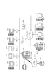
まず、変倍ブロック6から2タイル分の変倍処理が終了したことを示す信号が入力されるとタイルバッファ読み出し中であることを示す信号transを1にセットする。また、アドレスカウンタを0にリセットし、かつ、タイルの番号を示す信号oddを0にリセットする(S3201)。
【0240】
そして、タイルバッファより1画素ずつデータを読み出し、1タイル分のデータが読み出されるまでカウンタをカウントアップする(S3202:No,及びS3203)。
【0241】
1タイル分の変倍出力をタイルバッファより読み出し終えたら(S3202:Yes)、現在出力しているタイルバッファの内容が2タイル目であるかどうかを判断する(S3204)。
【0242】
2タイル目であるならば(S3204:No)、タイルバッファの読み出し終了動作を示す信号transを0にリセットする(S3205)。逆に、読み出したタイルバッファの内容が1タイル目であった場合には(S3204:Yes)、水平方向の最後の変倍結果であるかどうかの信号Xlastと、期待される出力タイル数が奇数であるかどうかを示す信号XdistOddを確認する(S3206)。
【0243】
ここで、水平方向の最終出力であり、かつ、期待される出力タイル数が奇数の場合(S3206:Yes)には、読み出しアドレスのカウントを中止し、trans信号を0にリセットする(S3205)。それ以外の場合(S3206:No)にはoddを1にセットし、カウンタを0にリセットした後(S3207)、ステップS3202に戻り、上記のカウントアップ動作を再度実行する。
【0244】
このように、書き込みアドレスカウンタ3001は、タイルバッファ7への書き込み制御を行うため、Valid信号が1のときにカウントアップ動作を行うカウンタで構成される。また、書き込みアドレスカウンタ3001は、タイルバッファ7への書き込み許可信号BufEnを出力するために、図33に示されるような回路にて構成される。
【0245】
図33の回路は、BufEnが1である場合にはタイルバッファ7への該当するラインへの書き込みデータ出力を変倍ブロック6に対し許可し、0である場合には変倍ブロック6のタイルバッファ7への該当するラインへの書き込みデータ出力処理を停止させることで、タイルバッファ7への書き込みを制御する。
【0246】
図33の回路は、タイルマスターインタフェース8が動作していない場合には、タイルバッファ7への書き込みを許可する。
【0247】
また、タイルマスターインタフェース8が動作中で、タイルマスターインタフェース8が最初のタイルを出力中の場合には、タイルバッファ7への書き込みを禁止する。
【0248】
また、タイルマスターインタフェース8が動作中で、タイルマスターインタフェース8が2番目のタイルを出力中の場合には、読み出し中のタイルのラインアドレスRdAddr_Lと書き込もうとしているラインアドレスから計算される値WrAdd_L+1の大きさを比較し、RdAddr_L>WrAdd_L+1である場合のみ書き込みを許可する。ここで、書き込みアドレスに対し+1が行われるのは、書き込み制御をライン単位で行わせることにより回路を簡単化するためである。
【0249】
以上説明したように、複数のタイルを一括して変倍処理する場合においても、有効な画像データのみを出力させるようにすることができる。
【0250】
(他の実施形態)
上記各実施形態の画像入出力装置は、複数の画像データに関する画像処理を並行に実行できるように構成されている。この画像入出力装置において、変倍処理を実行中、回転処理部等、他の画像処理部が画像メモリを同時に使用したとしても、本発明の適用により、互いの処理に関する画像メモリの競合を少なくすることができる。特に、画像入力インタフェースからの画像入力処理との並行処理を実行する際には、画像処理部において非常に大きな容量の画像データが同時に処理されることになる。しかし、この場合においても、画像メモリは各処理に関してタイル単位で確保されるので、円滑に並行処理を実行することができる。
【0251】
上記各実施形態では、デジタル複写機等の画像入出力装置を例に、本発明を説明してきたが、これに限るものではなく、本発明は複数の機器(例えば、ホストコンピュータ,インタフェース機器,リーダ,プリンタなど)から構成されるシステムに適用しても、一つの機器からなる装置(例えば、複写機,ファクシミリ装置など)等、様々な画像入出力装置に適用してもよい。
【0252】
また、本発明は、画像入出力装置に限らず、パーソナルコンピュータ等情報処理装置にも、適用可能である。この場合、例えば、上記画像入出力装置の変倍処理に係る部分をオプションカード上に構成し、そのオプションカードを情報処理装置の汎用バスに接続して用いる装置構成が考えられる。
【0253】
また、情報処理装置のCPUとメインメモリを上記変倍回路とし、画像処理専用の他のメモリを外部メモリとする装置構成をとるようにしても、本発明の処理は実行可能である。この場合、CPUが上記実施形態で説明した変倍処理のプログラムを実行することにより、メインメモリの記憶領域を節約することができる。このとき用いられる変倍処理のためのプログラムは、予め装置の記憶媒体等に格納されることになる。
【0254】
すなわち、本発明の目的は前述した実施形態の機能を実現するソフトウェアのプログラムコードを記録した記憶媒体を、システム或いは装置に供給し、そのシステム或いは装置のコンピュータ(CPU若しくはMPU)が記憶媒体に格納されたプログラムコードを読出し実行することによっても、達成されることは言うまでもない。
【0255】
この場合、記憶媒体から読出されたプログラムコード自体が前述した実施形態の機能を実現することになり、そのプログラムコードを記憶した記憶媒体は本発明を構成することになる。
【0256】
プログラムコードを供給するための記憶媒体としては、例えばフロッピー(R)ディスク,ハードディスク,光ディスク,光磁気ディスク,CD−ROM,CD−R,磁気テープ,不揮発性のメモリカード,ROMなどを用いることができる。
【0257】
また、コンピュータが読出したプログラムコードを実行することにより、前述した実施形態の機能が実現されるだけでなく、そのプログラムコードの指示に基づき、コンピュータ上で稼働しているOS(オペレーティングシステム)などが実際の処理の一部又は全部を行い、その処理によって前述した実施形態の機能が実現される場合も含まれることは言うまでもない。
【0258】
更に、記憶媒体から読出されたプログラムコードが、コンピュータに挿入された機能拡張ボードやコンピュータに接続された機能拡張ユニットに備わるメモリに書込まれた後、そのプログラムコードの指示に基づき、その機能拡張ボードや機能拡張ユニットに備わるCPUなどが実際の処理の一部又は全部を行い、その処理によって前述した実施形態の機能が実現される場合も含まれることは言うまでもない。
【0259】
同様に、本発明は、前述した実施形態の機能を実現するソフトウェアのプログラムコードを蓄積した外部装置(例えばアプリケーションサーバー等)から、ネットワークを介してダウンロードすることにより、システムあるいは装置の記憶装置に供給し、そのシステムあるいは装置のコンピュータ(またはCPUやMPU)がこの外部装置に格納されたプログラムコードを読み出し実行することによっても、完成されることは言うまでもない。
【0260】
【発明の効果】
以上説明してきたように、本発明によれば、少ないメモリ容量でタイル単位に変倍処理を行うことができるという効果がある。
【0261】
また、外部メモリを用いた画像処理、特に変倍処理を行う際の処理速度を向上させることができるという効果がある。
【0262】
また、簡単な構成で変倍処理と画像データの書き込み処理を行う際のメモリ管理を容易に効率よく行えるという効果がある。
【0263】
また、回路のクロック速度を上げることなく、変倍処理を行う際の処理速度を向上させることができるという効果がある。
【0264】
また、外部メモリを用いた変倍処理におけるデータ管理を容易にすることができるという効果がある。
【0265】
また、ICチップ内の回路構成にはほとんど影響を与えることなく、様々な変倍率や画像サイズに対応した変倍処理が可能となるという効果がある。
【図面の簡単な説明】
【図1】本発明を適用可能な画像入出力装置(デジタル複写機)の構成を説明するブロック図である。
【図2】システム制御部の構成を説明する詳細ブロック図である。
【図3】画像処理部の構成を説明する詳細ブロック図である。
【図4】図1の画像入出力装置を含むネットワークシステム全体の構成を説明する図である。
【図5】図1の画像入出力装置で用いられるデータパケットを説明するための図である。
【図6】図1の画像入出力装置で用いられるコマンドパケットを説明するための図である。
【図7】図1の画像入出力装置で用いられるインタラプトパケットを説明するための図である。
【図8】各パケットを管理するパケットテーブルを説明するための図である。
【図9】画像入力処理に関連するブロック間のデータの経路と処理手順を示す図である。
【図10】スキャナ2070で読み取った原稿画像のタイル画像への分割例を示す図である。
【図11】画像出力処理に関連するブロック間のデータの経路と処理手順を示す図である。
【図12】データパケットの変倍処理に関連するブロック間のデータの経路と処理手順を示す図である。
【図13】第1−3の実施形態における変倍処理部の構成を示す図である。
【図14】変倍ブロック6の詳細な構成を示すブロック図である。
【図15】外部メモリ上に展開されるタイル単位のラスタデータを示す図である。
【図16】図14に示した変倍コントロールブロックの詳細を示すブロック図である。
【図17】第2の実施形態におけるメモリインタフェース5の詳細な構成を示す図である。
【図18】図17に示した読み出し制御回路の詳細な構成を示す図である。
【図19】読み出し制御回路の動作を説明するためのタイミングチャートである。
【図20】図13に示したメモリインタフェースの一例を示す詳細ブロック図である。
【図21】図20に示した排他制御回路の詳細回路の一例を示すブロック図である。
【図22】図20に示した排他制御回路によるタイル画像データ転送処理時のメモリ状態を説明するための図である。
【図23】図20に示した排他制御回路によるタイル画像データ転送処理時のメモリ状態を説明するための図である。
【図24】図20に示した排他制御回路によるタイル画像データ転送処理時のメモリ状態を説明するための図である。
【図25】図20に示した排他制御回路によるタイル画像データ転送処理時のメモリ状態を説明するための図である。
【図26】第4、第5の実施形態における変倍処理部のブロック構成を示す図である。
【図27】第4の実施形態におけるタイルバッファ制御回路を示すブロック図である。
【図28】タイルバッファ7におけるアドレスの一例を示す図である。
【図29】タイル単位で処理を行う場合と、水平方向に2タイル連続して処理を行う場合との処理領域の違いを示す図である。
【図30】第5の実施形態におけるタイルバッファ制御回路を示すブロック図である。
【図31】タイルバッファのアドレス配置を説明するための図である。
【図32】読み出しアドレスカウンタが従うアドレス生成のためのフローである。
【図33】書き込みアドレスカウンタの回路構成を示す図である。
【図34】従来の変倍回路の動作概略を示す図である。
【図35】従来の変倍回路の詳細な構成を示すブロック図である。
【図36】フィルタ処理回路の動作を示す図である。
【符号の説明】
4 タイルスレーブインタフェース
5 メモリインタフェース
6 変倍ブロック
7 タイルバッファ
8 タイルマスターインタフェース
9 レジスタインタフェース
2116 変倍処理部
2123 画像(外部)メモリ[0001]
BACKGROUND OF THE INVENTION
The present invention relates to an image processing device, an image input / output device, a scaling processing method, and a memory control method for performing image processing, particularly scaling processing, on input image data.
[0002]
[Prior art]
Image scaling processing is a very important function in image input / output devices such as digital copying machines and information processing devices such as personal computers. Particularly in an image input / output device, this is a frequently used function, and a dedicated scaling circuit is usually provided.
[0003]
An outline of the operation of the conventional zoom circuit is shown in FIG. In FIG. 34, 3401 represents a scaling circuit, 3402 represents the entire original image (input image) to be scaled, and 3403 represents the entire output image after scaling.
[0004]
FIG. 35 is a block diagram showing a detailed configuration of a
[0005]
A
[0006]
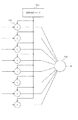
FIG. 36 is a diagram illustrating the operation of the filter processing circuit. In FIG. 36, 3601 is a filter coefficient generation circuit, 3602 is a multiplication circuit, and 3603 is an addition circuit. Here, filter coefficients are output from the filter
[0007]
By the way, as disclosed in JP-A-2002-8002, an image input / output apparatus in which each processing block performs image processing in units of tiles has been proposed by the present applicant. The configuration of the image processing unit of the image input / output device is suitable for an IC chip, and a magnification changing circuit can be provided as one of the processing blocks.
[0008]
[Problems to be solved by the invention]
However, with the recent enlargement of the image size handled, in the scaling circuit as in the conventional example, the buffer required for the scaling process becomes very large. In the case of the circuit shown in FIG. 35, the line buffer needs 8 lines. For example, in the case of an A4, 600 dpi original image, a buffer of about 7000 pixels is required.
[0009]
In particular, when a scaling circuit is mounted on the image input / output device that manages image data in units of tiles as described above, in the conventional scaling circuit, even if the scaling circuit is incorporated in one chip, the line buffer Since it would be huge, it was not practical for IC implementation.
[0010]
In addition, a device configuration in which an IC chip including a zoom circuit does not have a line buffer and uses a memory outside the manageable chip as a substitute for the line buffer is conceivable. However, with this configuration alone, access to the external memory is concentrated. However, the processing speed of the zoom circuit may be limited.
[0011]
SUMMARY An advantage of some aspects of the invention is that it provides an image processing apparatus and a scaling process method for an image processing apparatus that can perform a scaling process in tile units with a small memory capacity.
[0012]
It is another object of the present invention to provide an image processing apparatus and a memory control method for the image processing apparatus that improve the processing speed when performing image processing using an external memory, particularly, scaling processing.
[0013]
It is another object of the present invention to provide an image processing apparatus and a memory control method for the image processing apparatus that can easily and efficiently perform memory management when performing scaling processing and image data writing processing with a simple configuration.
[0014]
It is another object of the present invention to provide an image processing apparatus and a scaling process method of the image processing apparatus that improve the processing speed when performing scaling processing without increasing the clock speed of the circuit.
[0015]
It is another object of the present invention to provide an image input / output device that facilitates data management in a scaling process using an external memory and a scaling process method for the image input / output apparatus.
[0016]
Also provided are an image input / output device and an image input / output device scaling processing method capable of scaling processing corresponding to various scaling factors and image sizes with little influence on the circuit configuration in the IC chip. The purpose is to do.
[0017]
[Means for Solving the Problems]
In order to achieve the above object, an image processing apparatus of the present invention is an image processing apparatus that performs a scaling process on input image data, and divides the input image data into a plurality of tiles having a predetermined size. Dividing means for generating image data, compression means for compressing a plurality of tile image data generated by the dividing means, and generating a plurality of data packets including the compressed tile image data, and the compressing means Storage means for storing a plurality of data packets generated by the storage means, decompression means for reading out and decompressing tile image data included in each of the plurality of data packets stored in the storage means, and decompression processing by the decompression means The plurality of tile image data based on the plurality of data packets thus generated is subjected to a scaling process to generate a plurality of tile image data of the predetermined size When the scaling process is executed based on a plurality of data packets stored in the storage unit, the expansion unit, the scaling unit, the compression unit, and the storage unit. Adding means for adding header information for transferring a plurality of data packets to the plurality of data packets, and the decompression means outputs tile image data included in each of the plurality of data packets stored in the storage means. A plurality of data packets including the decompressed tile image data are transferred to the scaling unit based on the header information, and the scaling unit transfers the plurality of data transferred from the expansion unit. The tile image data included in each of the packets is subjected to a scaling process, and a plurality of data packets including the tile image data generated by the scaling process are transferred to the above-described packet. Based on the image information, the compression means compresses tile image data included in each of the plurality of data packets transferred from the scaling means, and the compressed tiles A plurality of data packets including image data are transferred to the storage means based on the header information.
[0023]
The scaling processing method of the present invention is a scaling processing method of an image processing apparatus having a scaling unit that executes scaling processing, a compression unit that executes compression processing, and a decompression unit that executes decompression processing. A dividing step of dividing the input image data to generate a plurality of tile image data of a predetermined size, and a plurality of tile image data generated by the dividing step is compressed by the compression unit A first compression step for generating a plurality of data packets including tile image data subjected to the compression processing, a first writing step for writing the plurality of data packets generated by the first compression step into a memory, and the memory When the scaling process is executed based on a plurality of data packets stored in the memory, the plurality of data packets are transferred in the order of the decompression unit, the scaling unit, the compression unit, and the memory. An adding step of adding header information to the plurality of data packets, and the tile image data included in each of the plurality of data packets written in the memory is decompressed by the decompression unit, and the decompression processing is performed. A plurality of data packets including the tile image data transferred to the scaling unit based on the header information, and the plurality of data packets transferred from the expansion unit to the scaling unit by the expansion step. Based on the header information, a plurality of data packets including the tile image data of the predetermined size generated by the scaling unit performing scaling processing on the tile image data included in each of the scaling unit. A scaling step transferred to the compression unit, and a tile included in each of the plurality of data packets transferred from the scaling unit to the compression unit by the scaling step. A second compression step of compressing the image data and transferring a plurality of data packets including the compressed tile image data to the memory based on the header information; and from the compression unit in the second compression step A second writing step of writing a plurality of previous data packets transferred to the memory into the memory.
[0025]
The scaling processing method of the present invention is a memory control method for an image processing apparatus that performs scaling processing on input image data. Split processing In memory plural Tile image Data Write process to write and before Memo Tile image written on Mori data A reading step of reading
Tile image read in the reading step data If the scaling process for scaling the image and the specified vertical scaling ratio is n (n <1), Memo Vertical tile image to be managed in Mori Data The number is at least (1 / n) +2, and before the reading step and the writing step Memo And an exclusive control process for performing exclusive control related to access to memory.
[0029]
DETAILED DESCRIPTION OF THE INVENTION
Hereinafter, embodiments according to the present invention will be described in detail with reference to the drawings.
[0030]
(First embodiment)
First, the configuration and operation of an image input / output device that divides a single image into a plurality of tiles and exchanges and manages image data in units of tiles will be described. This image input / output device is generally called a digital copying machine, and can execute a scaling process according to the present invention.
[0031]
[Configuration of image input / output device]
FIG. 1 is a block diagram for explaining the configuration of an image input / output apparatus (digital copying machine) to which the present invention can be applied. FIG. 2 is a detailed block diagram illustrating the configuration of the system control unit illustrated in FIG. 1, and FIG. 3 is a detailed block diagram illustrating the configuration of the image processing unit illustrated in FIG.
[0032]
1 to 3, the
[0033]
In FIG. 2, a
[0034]
The
[0035]
The sub bus switch 2128 is a second bus switch, and is connected to the image DMA (1) 2130, the image DMA (2) 2132, the
[0036]
In FIG. 1, a
[0037]
A ROM 2003 is a boot ROM, and stores a system boot program. The ROM 2003 is controlled by the ROM controller 2125 shown in FIG.
[0038]
In FIG. 2, an image DMA (1) 2130 is connected to the image compression unit 2131, controls the image compression unit 2131 based on information set via the register access ring 2137, and stores uncompressed data on the
[0039]
The image DMA (2) 2132 is connected to the
[0040]
The
[0041]
The
[0042]
The
[0043]
An operation unit I /
[0044]
The
[0045]
The general-purpose bus interface (1, 2) 2142 is a bus bridge that includes two identical bus interfaces and supports a standard IO bus. In the present embodiment, an example in which
[0046]
In FIG. 1, a hard disk drive (HDD) 2004 stores system software and image data. The HDD 2004 is connected to one
[0047]
The
[0048]
In FIG. 2, an image ring interface (1) 2147 and an image ring interface (2) 2148 connect the
[0049]
The
[0050]
The tile decompression unit (1, 2) 2103 is connected to the
[0051]
In addition to the connection to the image ring interface (4) 2102, the tile compression unit (1-3) 2106 is connected to the
[0052]
The
[0053]
The
[0054]
A rendering unit interface 2110, an
[0055]
The rendering unit interface 2110 functions as an interface for inputting a bitmap image generated by a rendering unit 2060 described later. The rendering unit 2060 and the rendering unit interface 2110 are connected by a general video signal 2111. The rendering unit interface 2110 is connected to the
[0056]
The
[0057]
The
[0058]
The
[0059]
The external
[0060]
The
[0061]
In FIG. 1, a scanner
[0062]
The printer
[0063]
[Unit configuration of image input / output device]
The
[0064]
The image memory (1, 2) 2123 is also provided independently on the controller board as an external memory of the
[0065]
[Network system configuration]
FIG. 4 is a diagram for explaining the configuration of the entire network system including the image input / output apparatus (digital copying machine) of FIG.
[0066]
In FIG. 4,
[0067]
[0068]
An
[0069]
Reference numeral 1006 denotes a WWW server that provides an HTML document to the LAN. The image input /
[0070]
A
[0071]
On the other hand, the image input /
[0072]
A
[0073]
[Packet structure]
Next, the format of a packet used for image data processing in this embodiment will be described. The
[0074]
(1) Data packet (Fig. 5)
The data packet shown in FIG. 5 is composed of tile-
[0075]
Hereinafter, information included in the
[0076]
PcktType 3004 identifies the packet type. The PcktType 3004 includes a repeat flag. If the
[0077]
A
[0078]
The data packet has a case where image data is compressed and a case where it is not compressed. In the present embodiment, as an example of the compression algorithm, JPEG is used for multi-valued colors (including multi-value gray scales), and Pacbits are used for binary values. The distinction between the case of compression and the case of non-compression is indicated by a
[0079]
The
[0080]
PacketByteLength 3012 indicates the total number of bytes of the packet. ImageDataByteLength3015 indicates the number of bytes of image data.
[0081]
(2) Command packet (FIG. 6)
The command packet shown in FIG. 6 is for accessing the register setting bus 2109. By using this packet, the
[0082]
The
[0083]
[0084]
On the other hand, the
[0085]
(3) Interrupt packet (Fig. 7)
The interrupt packet shown in FIG. 7 includes a
[0086]
When the
[0087]
The packet data section 5002
[0088]
The Chip ID 5004 stores an ID representing the
[0089]
[Packet table configuration]
Each packet described above is managed by a packet table 6001 as shown in FIG. The packet table 6001 is used as a pair with image data. When the image data is expanded in the
[0090]
When 0 bits are added to the value (pointer and length) of the packet table 6001, a packet top address (Packet Start Address) 6002 and a packet byte length (Packet Byte Length) 6005 are obtained. That is,
Packet Address Pointer (27 bits) + 5b00000 = Packet head address
PacketLength (11 bits) + 5b00000 = Packet Byte Length
It becomes.
[0091]
It is assumed that the packet table 6001 and the chain table (Chain Table) 6010 are not divided.
[0092]
The packet table 6001 is always arranged in the scanning direction, and arranged in the order of Yn / Xn = 000 / 000,000 / 001,000 / 002,. The entry of the packet table 6001 uniquely indicates one tile. The entry next to Yn / Xmax is Yn + 1 / X0.
[0093]
If the packet is exactly the same data as the previous packet, the packet is not stored in the memory, and the same packet address pointer and packet length as the previous entry are stored in the entry of the packet table 6001. .
[0094]
That is, one packet data is indicated by two table entries. In this case, the
[0095]
When the packet is divided into a plurality of parts by the chain DMA,
[0096]
The entry of the chain table 6010 is composed of a
[0097]
[Image input processing by data packet]
Next, an image input process in which image data read by the
[0098]
FIG. 9 is a diagram illustrating a data path between blocks and a processing procedure related to the image input process. Hereinafter, description will be made with reference to FIG. 9 in addition to the block diagram shown in FIG.
[0099]
First, when an image is read by the
[0100]
The
[0101]
The
[0102]
Next, the
[0103]
The tile compression unit (1) 2106 JPEG compresses the
[0104]
In this way, a data packet is generated from the image data read by the
[0105]
FIG. 10 shows an example of dividing an original image read by the
[0106]
[Image output processing by data packet]
Next, an image output process for printing by the
[0107]
FIG. 11 shows a data path between blocks and a processing procedure related to the image output processing. In the following description, please refer to FIG. 11 in addition to the block diagram of FIGS.
[0108]
First, the data packet output from the
[0109]
The image ring interface 2101 (3) selects the tile expansion unit (1) 2103 and transfers the image tile data. The selection of the tile expansion unit (1) 2103 is performed in accordance with the
[0110]
A tile decompression unit (1) 2103 decompresses the tile image of the data packet by JPEG and converts it to uncompressed image data. Next, the tile expansion unit (1) 2103 requests the
[0111]
The
[0112]
When this raster data is all expanded as raster data for 32 lines output by the
[0113]
[Composite processing of image input / output devices]
In the present embodiment, a copy process using the
[0114]
Further, after executing the image input process, the data packet of the
[0115]
Further, by converting the data packet in the
[0116]
In the image output process, a print process can be performed by inputting a tile image from a rendering unit 2060 that performs a rendering process based on data received from an external device.
[0117]
Further, it is possible to perform image processing in which a data packet in the
[0118]
The main processing that can be executed by the image input / output device of the present embodiment has been described above, but each processing block in the
[0119]
[Scaling by data packet]
Next, the scaling process by the data packet in this embodiment will be described in detail.
[0120]
In the following, a description will be given of an example of a process in which a data packet (tile image) stored in the
[0121]
FIG. 12 is a diagram illustrating a data path between blocks and a processing procedure related to the data packet scaling process. Hereinafter, description will be given with reference to FIG. 12 in addition to the block diagram shown in FIG.
[0122]
First, the
[0123]
Next, the data packet output from the
[0124]
The tile decompression unit (1) 2103 decompresses the transferred data packet by JPEG and converts it into uncompressed image data. Next, the tile expansion unit (1) 2103 makes a connection request to the
[0125]
FIG. 13 is a diagram illustrating a configuration of the
[0126]
In FIG. 13, reference numeral 4 denotes a tile slave interface, which is an interface for receiving a data packet from the tile expansion unit (1) 2103 via the
[0127]
In the
[0128]
The
[0129]
The tile data subjected to the scaling process is sequentially sent to the
[0130]
Then, the
[0131]
Next, the
[0132]
The tile compression unit (1) 2106 compresses the data packet using JPEG, and transfers the JPEG compressed data packet to the
[0133]
[Details of zoom processing]
Here, the scaling process of the
[0134]
FIG. 14 is a block diagram showing a detailed configuration of the
[0135]
FIG. 15 is a diagram showing tile unit raster data developed on the
[0136]
FIG. 16 is a block diagram showing details of the variable
[0137]
First, tile data input from the tile decompression unit (1) 2103 to the tile slave interface 4 via the
[0138]
On the other hand, the
[0139]
As described above, the tile data sent from the
[0140]
Here, the detailed configuration and operation of the above-described
[0141]
In response to the Done signal from the
[0142]
Here, the tile data is read from the
[0143]
Thereafter, when the horizontal scaling process for one tile line is completed (HDone signal), the
[0144]
As a result of the above operation, the
[0145]
Since the horizontal address of the next output tile is 0, the
[0146]
As described above, according to the present embodiment, the required line buffer length is the number of pixels in the horizontal direction of the tile, and assuming that the configuration of the vertical scaling filter is the same as that of the conventional example, one tile. When the number of horizontal pixels is 32 and the maximum number of pixels that can be processed is about 7000 pixels, the amount of line buffer required by the
[0147]
Since the memory for raster development of tile images is an external memory, the circuit scale in the IC chip can be used if the tile size is the same even when considering various scaling factors and larger image sizes. Can be handled with little effect.
[0148]
The scaling unit can raster-develop image data in an appropriate area on the external memory based on the coordinate information of the header of the data packet without being directly controlled by the CPU or the like. Data management in the used scaling process is easy.
[0149]
(Second Embodiment)
Even in the case of the apparatus configuration as in the first embodiment, a considerably large external memory may be required when the image data is full color. For example, an image of A4 long size and 600 dpi is about 7000 pixels, and assuming that the number of pixels in the vertical direction of one tile is 32, an external memory of about 1 Mbyte is required for raster development of 8-bit full-color image data with one tile width. Needed. Furthermore, since a plurality of tiles are required to perform reduction in the vertical direction particularly as a scaling process, the amount of memory required for raster development further increases.
[0150]
In consideration of such a situation, it is preferable in terms of cost to use a general-purpose SDRAM rather than an SRAM having a high latency as the external memory.
[0151]
However, in the scaling circuit, the start pixel position required for the scaling process and the number of required pixels differ depending on the scaling ratio. For this reason, when an SDRAM is used for the image memory, burst transfer of all necessary pixel data at a time is problematic in terms of processing and the amount of buffer. The conversion processing speed will not increase with time.
[0152]
In this embodiment, even when an image memory that causes a read waiting time, such as an SDRAM, is used by controlling the read data amount of image data rasterized in an external memory at the start of scaling processing, Enables high-speed scaling.
[0153]
[Details of zoom processing]
The block configuration of the
[0154]
In FIG. 17,
[0155]
FIG. 18 is a diagram showing a detailed configuration of the
[0156]
The operation of the zoom circuit having the above configuration will be described with reference to signals shown in the figure.
[0157]
Image data input from the tile expansion unit (1) 2103 to the tile slave interface 4 via the
[0158]
As in the first embodiment, the
[0159]
On the other hand, the
[0160]
Here, signals exchanged by the
[0161]
On the other hand, among the image data written in the
[0162]
Next, the operation of the
[0163]
At the same time, the issue counter of the request counter (ReqCount) 601 that counts the number of issued requests is reset to “0”, and the StartDone signal is set to “1”. The Req signal that has been unmasked by the AND
[0164]
When it is confirmed that the RAck signal is asserted to “1” (t1), the issue counter of the request counter (ReqCount) 601 is incremented by 1, and the read request generation circuit (RReqGen) 602 sets the value of the read address (RAddr). Increment as necessary (8 in this example). At the same time, the read counter (ReadCount) 603 increases the counter value by the number of beats of the read request. Since the counter value is no longer “0”, the CountZero signal is “0”, but since the StartDone signal output from the request counter (ReqCount) 601 is “1”, the output of the
[0165]
Next, the memory interface 405 that has finished the read request to the
[0166]
After that, when the
[0167]
However, since reading of data has already started at the present time, the value of the read counter (ReadCount) 603 is reduced by “1” from the value obtained by increasing the normal increment (in this example, “8”). Therefore, the value is increased by “7” from the previous value (t4).
[0168]
Since the buffer (FIFO) of the
[0169]
On the other hand, since the request counter (ReqCount) 601 completes reading for the number of stages of the buffer (FIFO) upon receipt of the current read request, it holds the current value, and the StartDone signal is deasserted to “0”. Thus, both the mask signals StartDone and CountZero become “0” regardless of the state of the signal (NotFull) indicating the buffer (FIFO) state of the scaling block 406. Accordingly, the output of the
[0170]
Here, the image data is read out smoothly from the
[0171]
In the present embodiment, the scaling block 406 smoothly performs image data processing, and as a result, the buffer is not full. Of course, the amount of image data consumed varies depending on the magnification setting, the buffer is almost full, and a signal (NotFull) indicating the buffer state may be “0”. In this case, of course, no read request is generated.
[0172]
Thereafter, when a read request is accepted by the
[0173]
As described above, according to the present embodiment, for each tile, image data corresponding to the amount of the buffer of the horizontal scaling circuit is stored in the memory at the start of the horizontal scaling process regardless of the processing state of the scaling processing circuit. Transfer from the interface. As a result, it is possible to reduce image data required when the horizontal scaling circuit performs processing from waiting to be read from the memory interface, and to increase the processing speed.
[0174]
Further, by concentrating the reading process, the hit rate of the external SDRAM can be increased, and the writing speed at raster development can be increased for both the functional block using the external SDRAM in the IC chip.
[0175]
Furthermore, it is difficult to read out all the data amount required at the start of processing, such as scaling, and it is possible to easily perform read control that supports split transactions in a system that must be read sequentially.
[0176]
As described above, the scaling processing unit using the external SDRAM has been described as an example. However, the invention in this embodiment can be applied not only to the scaling processing unit but also to image processing in other processing blocks.
[0177]
For example, in the tile image generation process in the image input process of FIG. 9, the
[0178]
(Third embodiment)
When scaling processing is performed using an external memory as in the above embodiment, exclusive control is performed on writing and reading of tile images to the external memory in order to manage the memory and improve processing reliability. It is preferable. In the present embodiment, by adopting the exclusive control configuration described below, the memory management according to the scaling factor can be executed with a simple device configuration.
[0179]
[Details of zoom processing]
The block configuration of the
[0180]
In FIG. 20, a
[0181]
[0182]
FIG. 21 is a block diagram showing an example of a detailed circuit of the
[0183]
In FIG. 21, 801 is an exclusive OR gate, 802 is a D-FlipFlop, 803 is a D-FlipFlop with Enable, 804 is a decoder circuit, 805-1-s0 to 805-1-s7, 805-2-m0 to 805-2 -M7 is an And circuit, 806-1 to 806-8 are RS-FlipFlops, 807 is a mask generation circuit (MaskGen), and 808 is an AND gate.
[0184]
22 to 25 are diagrams for explaining a memory state at the time of tile image data transfer processing by the
[0185]
22 to 25, tFlag0 to 7 are flags indicating whether or not the scaling process of the tile position in the same vertical direction that changes according to the progress of the scaling process is completed. A memory state corresponding to the position is held on the RS-FlipFlop 806-1 to 806-8.
[0186]
The RS-FlipFlops 806-1 to 806-8 are set (“1”) or reset (“0”) based on the output of the
[0187]
In this embodiment, in FIG. 22 to FIG. 25, the minimum magnification that can be scaled by the scaling device is, for example, 0.25 (1/4), and the number of tiles in the vertical direction of the raster memory is a conditional expression. Since it is the minimum value (4 + 2 = 6) obtained more, it will be described as “8”, which is a power value of 2 that is more than this and is minimum.
[0188]
At the start of the zooming operation, the
[0189]
In the example shown in FIG. 22, it is assumed that data transfer has been completed for the third from the left at the top, and the fourth tile image indicated by the diagonal lines in FIG. 22 is currently being transferred.
[0190]
Then, the tile image transfer further proceeds, the transfer of the uppermost column in FIG. 22 is completed, and the transfer of the second column from the top is started as shown in FIG. The indicated flag tFlag0 is set to “1”. Similarly, the corresponding flags are sequentially set to “1” when the column writing is completed.
[0191]
On the other hand, in the control on the reading side by the scaling process, for example, the memory state in the case of performing the 1/4 magnification is as shown in FIG. 24. In FIG. Using the image data included in the tiles (3, 8n) to (8, 8n + 5) shown, an attempt is made to output the scaling result for one tile.
[0192]
Originally, since the scaling factor is 1/4 (both horizontal and vertical in this example), an image of 4 tiles (in this example, (4, 8n + 1) to (7, 8n + 4)) in both the horizontal and vertical directions. However, it is necessary to include peripheral image data because of the filter processing, so it is included in tiles (3, 8n) to (8, 8n + 5) as shown in FIG. Image data is required.
[0193]
FIG. 25 shows the state diagram of the memory and the flag value when the scaling process is executed in the horizontal direction from this state, the scaling process in the horizontal direction is finished, and one tile is processed as the scaling result in the vertical direction. As shown.
[0194]
As shown in FIG. 25, that is, when the memory state of FIG. 24 is shifted to the memory state of FIG. 25, the position of the tile image used for the scaling process is (0,8n + 4) to (4,8 (n + 1). ) Move to position +1). However, the tile images at positions (0,8 (n + 1)) to (4,8 (n + 1) +1) are the same as the tile images in FIG. 24, but are newly obtained from tile slaves. Since it is necessary to store image data, the corresponding
[0195]
An example of a circuit that realizes the setting and clearing of the corresponding flag corresponding to the changes in FIGS. 22 to 23 and FIGS. 24 to 25 is an
[0196]
When the writing of image data in one vertical direction is completed, that is, when the memory state shown in FIG. 22 changes to the memory state shown in FIG. 23, the vertical in the information (signal Tpos) indicating the position of the tile input from the tile slave interface 4 Direction information (signal Tpos (V) shown in FIG. 20) changes. Therefore, the timing of the change is captured, the position signal currently being written output from the
[0197]
On the other hand, when the scaling process for one vertical direction is completed, that is, when the memory state shown in FIG. 23 changes to the memory state shown in FIG. 24, the read address of the horizontal position from the memory is “0”. Therefore, the flag is cleared by enabling the output of the mask generation circuit 27 with the tile scaling start pulse (signal TileStart) when the horizontal read address is “0”.
[0198]
Also, the
[0199]
[Table 1]
Based on this flag data, it is determined whether or not the image data at the tile position to be written has already been read by the scaling process at the time of writing. If reading by the scaling process has been completed, the tile slave interface 4 receives data by setting the signal TEnable to “1” shown in FIG. On the other hand, when reading by the scaling process is not completed, the tile slave interface 4 corresponds to the
[0201]
On the other hand, at the time of reading, if the flag of the address to be read is set, the TRENable signal output from the
[0202]
On the other hand, when the flag is not set, the
[0203]
In the above embodiment, the write control signal TEnable is output to the tile slave interface and the transfer of tile data is limited. However, even if this signal is output to the
[0204]
According to this embodiment, exclusive control for writing and reading memory for raster conversion of tile images is performed in units of vertical tiles, and the scaling processing unit can process the number of vertical tiles to be managed When the minimum magnification is n (<1), memory management is easily realized by limiting the number of tiles in the vertical direction to be managed to (1 / n) +2 or more and a power of 2.
[0205]
Also, the release of the read-out memory due to special circumstances of the scaling processing unit can be easily realized by performing it at the time when the vertical output tile changes.
[0206]
Note that the number of vertical tiles to be managed is not limited to a power of two. That is, in the configuration of the above embodiment, even if the number of tiles in the vertical direction is six or seven, memory management can be similarly simplified.
[0207]
(Fourth embodiment)
When the device described in each of the above embodiments is integrated into an IC chip, it is possible to execute a scaling process that is somewhat fast, but it is expected that further speeding up of the scaling process will be required in the future.
[0208]
By increasing the clock speed of the entire circuit, it is possible to configure a circuit that satisfies this requirement, but this imposes restrictions on the implementation of an IC. Further, since the required speed of the external memory is also increased with the increase of the clock speed, it becomes a factor to increase the cost of the memory chip to be used.
[0209]
In this embodiment, instead of adding a few circuits to the scaling processing circuit, the scaling processing can be performed at a higher clock speed than the conventional one at the same clock speed.
[0210]
[Details of zoom processing]
A block diagram of the
[0211]
The detailed configuration of the
[0212]
However, unlike the above-described embodiments, the scaling
[0213]
First, tile data input from the tile expansion unit (1) 2103 to the tile slave interface 4 via the
[0214]
On the other hand, the
[0215]
Here, the detailed configuration and operation of the above-described
[0216]
In response to the Done signal from the
[0217]
Here, tile data is read from the
[0218]
Thereafter, when the horizontal scaling process for twice the number of pixels for one tile is completed (HDone signal), the
[0219]
When a predetermined scaling result is obtained in the
[0220]
On the other hand, the tile
[0221]
An example of the tile
[0222]
In order to clearly describe the characteristics of the scaling process of the present embodiment, the tile size is assumed to be 8 pixels in the horizontal direction and 8 lines in the vertical direction. An example of the address in the
[0223]
When writing to the
[0224]
Next, the processing time per tile line when the scaling process is performed using the configuration of the present embodiment is estimated. First, FIG. 29 shows the difference in processing area between when processing is performed in units of tiles and when processing is performed continuously in two tiles in the horizontal direction. FIG. 29 shows the original image data necessary for processing when the scaling factor is 1 (that is, 100%) and output tiles for simplicity. FIG. 29A illustrates a case where processing is performed in units of tiles, and hatched portions are image data that needs to be read from the external memory. As shown in the figure, since processing is performed in units of tiles, the hatched portion in the middle dark color actually needs to be read from the external memory twice (the end of the first tile and the beginning of the next tile). is there.
[0225]
FIG. 29B shows the processing result of this embodiment in which two tiles are output continuously. In FIG. 29B, since two tiles continuous in the horizontal direction are processed at a time, there is no area that must be read twice from the
[0226]
Next, an approximation of clock cycles required for processing per line when the magnification is 1 is performed. The delay between the start of processing and the output of image data from the memory interface cannot be avoided as long as an external memory is used. The number of cycles from when a read request is made until the data is actually read out is horizontal. This is an unnecessary cycle in which the zoom circuit cannot operate. This number of cycles is TA.
[0227]
Also, reading from the memory requires burst reading because of high-speed access, and the reading start position does not always match the pixel position that is actually required for scaling processing. Cycle occurs and its value is TB.
[0228]
Let TC be the overhead at the start of the scaling operation and the number of cycles required to complete the pipeline processing.
[0229]
The actual number of horizontal processing cycles is calculated under the above conditions. However, if TA, TB, and TC are used as representative values of 10, 7, and 5, respectively, the horizontal scaling of the number of pixels corresponding to one tile is obtained. The processing cycle required is
TA + TB + 32 + TC = 54
On the other hand, if you want to batch process horizontal scaling for two consecutive tiles
TA + TB + 64 + TC = 86
If this is converted to one tile, it will be half that, so 86/2 = 43
Therefore, on average, the processing cycle can be shortened by about 20%, that is, the processing speed can be increased.
[0230]
As described above, in this embodiment, since two tiles are processed, high-speed scaling processing can be performed without increasing the clock speed or the like. Note that the number of tiles to be processed at a time is not limited to two, and three or four tiles may be processed at a time.
[0231]
(Fifth embodiment)
In the fourth embodiment, since a plurality of tiles are subjected to scaling processing in a lump, even data that is not originally required may be output from the scaling block when processing at the edge in the horizontal direction.
[0232]
In this embodiment, even when scaling processing is performed in units of a plurality of tiles, the scaling processing unit is controlled so that only valid tiles are output.
[0233]
[Details of zoom processing]
The block configuration of the
[0234]
FIG. 30 shows a block diagram of the tile buffer control circuit of this embodiment. In FIG. 30,
[0235]
FIG. 31 is a diagram for explaining the address arrangement of the tile buffer. Now, as shown in FIG. 31 (a), if the tile buffer is used by securing an area for two tiles in the horizontal direction, the address at the time of writing has an address arrangement as shown in the figure, The lower 6 bits are occupied by the horizontal pixel counter, and the upper 5 bits are occupied by the line direction counter.
[0236]
On the other hand, as shown in FIG. 31 (b), the address at the time of reading the tile data stored in the tile buffer indicates whether it is an even-numbered tile or an odd-numbered tile in the horizontal direction because it needs to be read in tile units. The lower 5 bits are occupied by the horizontal pixel address in the tile, and the upper 5 bits are occupied by the vertical line address.
[0237]
In order to correctly generate an address at the time of reading, the read address counter generates an address according to a flow as shown in FIG.
[0238]
The processing of the flowchart of FIG. 32 is controlled by a CPU (not shown) incorporated in the
[0239]
First, when a signal indicating that scaling processing for two tiles has been completed is input from the
[0240]
Then, data is read pixel by pixel from the tile buffer, and the counter is counted up until data for one tile is read (S3202: No, and S3203).
[0241]
When the scaling output for one tile has been read from the tile buffer (S3202: Yes), it is determined whether or not the content of the currently output tile buffer is the second tile (S3204).
[0242]
If it is the second tile (S3204: No), the signal trans indicating the tile buffer read end operation is reset to 0 (S3205). On the other hand, when the content of the read tile buffer is the first tile (S3204: Yes), the signal Xlast indicating whether or not the final scaling result in the horizontal direction and the expected number of output tiles are odd numbers. The signal XdistOdd indicating whether or not is confirmed (S3206).
[0243]
If the output is the final output in the horizontal direction and the expected number of output tiles is an odd number (S3206: Yes), the count of the read address is stopped and the trans signal is reset to 0 (S3205). In other cases (S3206: No), odd is set to 1 and the counter is reset to 0 (S3207). Then, the process returns to step S3202, and the count-up operation is performed again.
[0244]
As described above, the
[0245]
The circuit shown in FIG. 33 permits the
[0246]
The circuit in FIG. 33 permits writing to the
[0247]
In addition, when the
[0248]
When the
[0249]
As described above, even when a plurality of tiles are collectively subjected to scaling processing, only valid image data can be output.
[0250]
(Other embodiments)
The image input / output device of each of the above embodiments is configured so that image processing relating to a plurality of image data can be executed in parallel. In this image input / output device, even when another image processing unit such as a rotation processing unit uses the image memory at the same time during the scaling process, the application of the present invention reduces the contention of the image memory related to each other processing. can do. In particular, when executing parallel processing with image input processing from the image input interface, a very large amount of image data is simultaneously processed in the image processing unit. However, even in this case, since the image memory is secured in tile units for each process, parallel processing can be executed smoothly.
[0251]
In each of the above-described embodiments, the present invention has been described by taking an image input / output device such as a digital copying machine as an example. However, the present invention is not limited to this, and the present invention includes a plurality of devices (for example, a host computer, an interface device, a reader). The present invention may be applied to a system composed of a printer, etc., or to various image input / output devices such as a device composed of a single device (for example, a copying machine, a facsimile machine, etc.).
[0252]
The present invention is not limited to an image input / output device but can be applied to an information processing device such as a personal computer. In this case, for example, a device configuration in which a portion related to the scaling process of the image input / output device is configured on an option card and the option card is connected to a general-purpose bus of the information processing device can be considered.
[0253]
Further, the processing of the present invention can be executed even if the CPU and the main memory of the information processing apparatus have the above-described scaling circuit and the other memory dedicated to image processing is an external memory. In this case, the CPU can save the storage area of the main memory by executing the scaling process program described in the above embodiment. The scaling process program used at this time is stored in advance in a storage medium of the apparatus.
[0254]
In other words, an object of the present invention is to supply a storage medium storing software program codes for realizing the functions of the above-described embodiments to a system or apparatus, and store the computer (CPU or MPU) of the system or apparatus in the storage medium. Needless to say, this can also be achieved by reading and executing the programmed program code.
[0255]
In this case, the program code itself read from the storage medium realizes the functions of the above-described embodiments, and the storage medium storing the program code constitutes the present invention.
[0256]
As a storage medium for supplying the program code, for example, a floppy (R) disk, a hard disk, an optical disk, a magneto-optical disk, a CD-ROM, a CD-R, a magnetic tape, a nonvolatile memory card, a ROM, or the like is used. it can.
[0257]
Further, by executing the program code read by the computer, not only the functions of the above-described embodiments are realized, but also an OS (operating system) operating on the computer based on the instruction of the program code. It goes without saying that a case where the function of the above-described embodiment is realized by performing part or all of the actual processing and the processing is included.
[0258]
Further, after the program code read from the storage medium is written into a memory provided in a function expansion board inserted into the computer or a function expansion unit connected to the computer, the function expansion is performed based on the instruction of the program code. It goes without saying that the CPU or the like provided in the board or the function expansion unit performs part or all of the actual processing and the functions of the above-described embodiments are realized by the processing.
[0259]
Similarly, the present invention supplies a system or device storage device by downloading it from an external device (for example, an application server) that stores software program codes that implement the functions of the above-described embodiments via a network. Needless to say, the computer or the computer (or CPU or MPU) of the system or apparatus reads out and executes the program code stored in the external apparatus.
[0260]
【The invention's effect】
As described above, according to the present invention, there is an effect that the scaling process can be performed in tile units with a small memory capacity.
[0261]
Further, there is an effect that it is possible to improve the processing speed when performing image processing using an external memory, particularly scaling processing.
[0262]
Further, there is an effect that memory management can be easily and efficiently performed when performing scaling processing and image data writing processing with a simple configuration.
[0263]
Further, there is an effect that the processing speed when performing the scaling process can be improved without increasing the clock speed of the circuit.
[0264]
In addition, there is an effect that data management in scaling processing using an external memory can be facilitated.
[0265]
In addition, there is an effect that scaling processing corresponding to various scaling factors and image sizes can be performed without substantially affecting the circuit configuration in the IC chip.
[Brief description of the drawings]
FIG. 1 is a block diagram illustrating a configuration of an image input / output apparatus (digital copying machine) to which the present invention is applicable.
FIG. 2 is a detailed block diagram illustrating a configuration of a system control unit.
FIG. 3 is a detailed block diagram illustrating a configuration of an image processing unit.
4 is a diagram for explaining a configuration of an entire network system including the image input / output device of FIG. 1;
5 is a diagram for explaining a data packet used in the image input / output device of FIG. 1; FIG.
6 is a diagram for explaining a command packet used in the image input / output device of FIG. 1; FIG.
7 is a diagram for explaining an interrupt packet used in the image input / output device of FIG. 1; FIG.
FIG. 8 is a diagram for explaining a packet table for managing each packet;
FIG. 9 is a diagram illustrating a data path between blocks and a processing procedure related to image input processing;
10 is a diagram illustrating an example of dividing an original image read by a
FIG. 11 is a diagram illustrating a data path between blocks and a processing procedure related to image output processing;
FIG. 12 is a diagram illustrating a data path between blocks and a processing procedure related to a data packet scaling process;
FIG. 13 is a diagram illustrating a configuration of a scaling processing unit in the first to third embodiments.
FIG. 14 is a block diagram showing a detailed configuration of a
FIG. 15 is a diagram showing raster data in units of tiles developed on an external memory.
FIG. 16 is a block diagram showing details of a scaling control block shown in FIG. 14;
FIG. 17 is a diagram showing a detailed configuration of a
18 is a diagram showing a detailed configuration of the read control circuit shown in FIG.
FIG. 19 is a timing chart for explaining the operation of the read control circuit;
20 is a detailed block diagram showing an example of the memory interface shown in FIG. 13;
FIG. 21 is a block diagram showing an example of a detailed circuit of the exclusive control circuit shown in FIG. 20;
22 is a diagram for explaining a memory state at the time of tile image data transfer processing by the exclusive control circuit shown in FIG. 20;
23 is a diagram for explaining a memory state at the time of tile image data transfer processing by the exclusive control circuit shown in FIG. 20;
24 is a diagram for explaining a memory state at the time of tile image data transfer processing by the exclusive control circuit shown in FIG. 20;
25 is a diagram for explaining a memory state at the time of tile image data transfer processing by the exclusive control circuit shown in FIG. 20;
FIG. 26 is a diagram illustrating a block configuration of a scaling processing unit in the fourth and fifth embodiments.
FIG. 27 is a block diagram illustrating a tile buffer control circuit according to a fourth embodiment.
FIG. 28 is a diagram illustrating an example of addresses in the
FIG. 29 is a diagram illustrating a difference in processing region between when processing is performed in units of tiles and when processing is performed continuously for two tiles in the horizontal direction.
FIG. 30 is a block diagram illustrating a tile buffer control circuit according to a fifth embodiment.
FIG. 31 is a diagram for explaining an address arrangement of a tile buffer.
FIG. 32 is a flow for address generation according to a read address counter.
FIG. 33 is a diagram showing a circuit configuration of a write address counter.
FIG. 34 is a diagram showing an outline of the operation of a conventional zoom circuit.
FIG. 35 is a block diagram showing a detailed configuration of a conventional zoom circuit.
FIG. 36 is a diagram illustrating an operation of a filter processing circuit.
[Explanation of symbols]
4 Tile slave interface
5 Memory interface
6 Scaling block
7 Tile buffer
8 Tile master interface
9 Register interface
2116 Scaling processing unit
2123 Image (external) memory
Claims (4)
入力した画像データを分割処理して所定の大きさの複数のタイル画像データを生成する分割手段と、
前記分割手段により生成された複数のタイル画像データを圧縮処理して該圧縮処理されたタイル画像データを含む複数のデータパケットを生成する圧縮手段と、
前記圧縮手段により生成された複数のデータパケットを記憶する記憶手段と、
前記記憶手段に記憶された複数のデータパケットの各々に含まれるタイル画像データを読み出して伸張処理する伸張手段と、
前記伸張手段により伸張処理された複数のデータパケットに基づく複数のタイル画像データを変倍処理して前記所定の大きさの複数のタイル画像データを生成する変倍手段と、
前記記憶手段に記憶された複数のデータパケットに基づいて前記変倍処理を実行させる場合に、前記伸張手段、前記変倍手段、前記圧縮手段、前記記憶手段の順で前記複数のデータパケットを転送させるためのヘッダ情報を前記複数のデータパケットに付加する付加手段とを有し、
前記伸張手段は前記記憶手段に記憶された複数のデータパケットの各々に含まれるタイル画像データを伸張処理して、該伸張処理されたタイル画像データを含む複数のデータパケットを前記ヘッダ情報に基づいて前記変倍手段へ転送し、
前記変倍手段は前記伸張手段から転送された前記複数のデータパケットの各々に含まれるタイル画像データを変倍処理して、該変倍処理により生成されたタイル画像データを含む複数のデータパケットを前記ヘッダ情報に基づいて前記圧縮手段へ転送し、
前記圧縮手段は、前記変倍手段から転送された前記複数のデータパケットの各々に含まれるタイル画像データを圧縮処理して、該圧縮処理されたタイル画像データを含む複数のデータパケットを前記ヘッダ情報に基づいて前記記憶手段に転送することを特徴とする画像処理装置。An image processing apparatus that performs a scaling process on input image data,
A dividing means for dividing the input image data to generate a plurality of tile image data of a predetermined size ;
Compression means for compressing a plurality of tile image data generated by the dividing means and generating a plurality of data packets including the compressed tile image data;
Storage means for storing a plurality of data packets generated by the compression means;
And decompressing means for decompressing process reads the filter yl image data included in each of the plurality of data packets stored in said storage means,
And scaling means for generating a variable magnification process by a plurality of tile image data of said predetermined size with a plurality of tile image data based on a plurality of data packets decompressed by said decompressing means,
When the scaling process is executed based on a plurality of data packets stored in the storage unit, the plurality of data packets are transferred in the order of the expansion unit, the scaling unit, the compression unit, and the storage unit. Adding means for adding header information to the plurality of data packets ,
The decompressing means decompresses tile image data included in each of the plurality of data packets stored in the storage means, and the plurality of data packets including the decompressed tile image data are processed based on the header information. Forward to the scaling means,
The scaling unit performs scaling processing on tile image data included in each of the plurality of data packets transferred from the decompression unit, and generates a plurality of data packets including tile image data generated by the scaling processing. Transfer to the compression means based on the header information;
The compression unit compresses tile image data included in each of the plurality of data packets transferred from the scaling unit , and converts the plurality of data packets including the compressed tile image data into the header information. The image processing apparatus transfers to the storage means based on the above .
前記データパケットは、前記複数の画像処理手段及び前記変倍手段のいずれで処理されるべきかを示すヘッダ情報を含むことを特徴とする請求項1に記載の画像処理装置。A plurality of image processing means for generating a plurality of tile image data by performing image processing on a plurality of data packets decompressed by the decompression means;
The image processing apparatus according to claim 1, wherein the data packet includes header information indicating which of the plurality of image processing units and the scaling unit should be processed.
前記データパケットに含まれるヘッダ情報に基づいて、前記データパケットを前記複数の画像処理手段及び前記変倍手段のいずれかに転送するバスインターフェースとを有することを特徴とする請求項2に記載の画像処理装置。A bus to which the plurality of image processing means and the scaling means are connected;
3. The image according to claim 2 , further comprising: a bus interface that transfers the data packet to any of the plurality of image processing units and the scaling unit based on header information included in the data packet. Processing equipment.
入力した画像データを分割処理して所定の大きさの複数のタイル画像データを生成する分割工程と、
前記分割工程により生成された複数のタイル画像データを前記圧縮部にて圧縮処理して該圧縮処理されたタイル画像データを含む複数のデータパケットを生成する第1圧縮工程と、
前記第1圧縮工程により生成された複数のデータパケットをメモリに書き込む第1書込工程と、
前記メモリに記憶された複数のデータパケットに基づいて前記変倍処理を実行させる場合に、前記伸張部、前記変倍部、前記圧縮部、前記メモリの順で前記複数のデータパケットを転送させるためのヘッダ情報を前記複数のデータパケットに付加する付加工程と、
前記メモリに書き込まれた複数のデータパケットの各々に含まれるタイル画像データを前記伸張部にて伸張処理して、該伸張処理されたタイル画像データを含む複数のデータパケットを前記ヘッダ情報に基づいて前記変倍部へ転送する伸張工程と、
前記伸張工程により前記伸張部から前記変倍部に転送された前記複数のデータパケットの各々に含まれるタイル画像データを前記変倍部にて変倍処理して該変倍処理により生成 された前記所定の大きさのタイル画像データを含む複数のデータパケットを前記ヘッダ情報に基づいて前記圧縮部に転送する変倍工程と、
前記変倍工程により前記変倍部から前記圧縮部に転送された前記複数のデータパケットの各々に含まれるタイル画像データを圧縮処理して該圧縮処理されたタイル画像データを含む複数のデータパケットを前記ヘッダ情報に基づいて前記メモリに転送する第2圧縮工程と、
前記第2圧縮工程にて前記圧縮部から前記メモリに転送された前複数のデータパケットを前記メモリに書き込む第2書込工程と、
を有することを特徴とする変倍処理方法。A scaling process method for an image processing apparatus having a scaling unit for executing scaling processing , a compression unit for executing compression processing, and a decompression unit for executing decompression processing ,
A dividing step of dividing the input image data to generate a plurality of tile image data of a predetermined size ;
A first compression step of generating a plurality of data packets including the compressed tile image data by compressing the plurality of tile image data generated by the dividing step by the compression unit ;
A first writing step of writing a plurality of data packets generated by the first compression step into a memory;
To transfer the plurality of data packets in the order of the expansion unit, the scaling unit, the compression unit, and the memory when the scaling process is executed based on the plurality of data packets stored in the memory An additional step of adding the header information to the plurality of data packets;
Said filter yl image data included in each of the plurality of data packets written to memory by decompression processing by the decompression unit, a plurality of data packets including the tile image data該伸Zhang processing on the header information An expansion step of transferring to the zooming unit based on ;
Said generated by scaling process to variable magnification processing tile image data included from the decompression the expansion section by the processes to each of the plurality of data packets transferred to the scaling unit at the scaling unit A scaling step of transferring a plurality of data packets including tile image data of a predetermined size to the compression unit based on the header information ;
A plurality of data packets including the tile image data subjected to the compression processing by compressing the tile image data included in each of the plurality of data packets transferred from the scaling unit to the compression unit by the scaling step. A second compression step of transferring to the memory based on the header information;
A second writing step of writing a plurality of data packets prior to being transferred to the memory from the compression section at the second compression step to the memory,
Scaling method characterized by having a.
Priority Applications (3)
| Application Number | Priority Date | Filing Date | Title |
|---|---|---|---|
| JP2002202918A JP4065503B2 (en) | 2001-08-21 | 2002-07-11 | Image processing apparatus, image input / output apparatus, scaling process method, and memory control method |
| US10/216,767 US7065263B2 (en) | 2001-08-21 | 2002-08-13 | Image processing apparatus, image input/output apparatus, scaling method and memory control method |
| US11/334,585 US7286720B2 (en) | 2001-08-21 | 2006-01-19 | Image processing apparatus, image input/output apparatus, scaling method and memory control method |
Applications Claiming Priority (4)
| Application Number | Priority Date | Filing Date | Title |
|---|---|---|---|
| JP2001250406 | 2001-08-21 | ||
| JP2001250407 | 2001-08-21 | ||
| JP2002138343 | 2002-05-14 | ||
| JP2002202918A JP4065503B2 (en) | 2001-08-21 | 2002-07-11 | Image processing apparatus, image input / output apparatus, scaling process method, and memory control method |
Publications (3)
| Publication Number | Publication Date |
|---|---|
| JP2004048372A JP2004048372A (en) | 2004-02-12 |
| JP2004048372A5 JP2004048372A5 (en) | 2006-04-06 |
| JP4065503B2 true JP4065503B2 (en) | 2008-03-26 |
Family
ID=27482510
Family Applications (1)
| Application Number | Title | Priority Date | Filing Date |
|---|---|---|---|
| JP2002202918A Expired - Fee Related JP4065503B2 (en) | 2001-08-21 | 2002-07-11 | Image processing apparatus, image input / output apparatus, scaling process method, and memory control method |
Country Status (2)
| Country | Link |
|---|---|
| US (2) | US7065263B2 (en) |
| JP (1) | JP4065503B2 (en) |
Families Citing this family (28)
| Publication number | Priority date | Publication date | Assignee | Title |
|---|---|---|---|---|
| US7315388B2 (en) * | 2001-01-24 | 2008-01-01 | Canon Kabushiki Kaisha | Image input/output control apparatus, image processing apparatus, image processing method, data communication apparatus, and data communication method |
| AUPR947701A0 (en) * | 2001-12-14 | 2002-01-24 | Activesky, Inc. | Digital multimedia publishing system for wireless devices |
| JP4109151B2 (en) * | 2003-04-23 | 2008-07-02 | オリンパス株式会社 | Image processing device |
| WO2005015504A1 (en) * | 2003-08-07 | 2005-02-17 | Renesas Technology Corp. | Image processing semiconductor processor |
| JP4110076B2 (en) * | 2003-11-21 | 2008-07-02 | キヤノン株式会社 | Image processing apparatus and image processing method |
| US6999105B2 (en) * | 2003-12-04 | 2006-02-14 | International Business Machines Corporation | Image scaling employing horizontal partitioning |
| US8705141B2 (en) * | 2004-07-16 | 2014-04-22 | Ricoh Production Print Solutions | Method and system for efficiently printing simple data using a complex page data stream |
| JP2006067577A (en) * | 2004-08-26 | 2006-03-09 | Oce Technologies Bv | Method, apparatus and computer program product for processing image data stored on memory for rendering image on device |
| US20060050089A1 (en) * | 2004-09-09 | 2006-03-09 | Atousa Soroushi | Method and apparatus for selecting pixels to write to a buffer when creating an enlarged image |
| US20070122045A1 (en) * | 2005-11-29 | 2007-05-31 | Jiun-Yuan Wu | System for scaling a picture unit from a first video resolution format to a second video resolution format |
| FR2896324A1 (en) * | 2006-01-17 | 2007-07-20 | St Microelectronics Sa | PROCESSING METHOD, FOR EXAMPLE OF COLOR INSERTION OF A DIGITAL IMAGE AND CORRESPONDING DEVICE |
| US8643661B1 (en) | 2006-06-21 | 2014-02-04 | Marvell International Ltd. | Non raster row pixel processing |
| US7659897B1 (en) * | 2006-06-30 | 2010-02-09 | Nvidia Corporation | System, method, and computer program product for video benchmarking |
| US7839424B1 (en) * | 2006-07-13 | 2010-11-23 | Marvell International Ltd. | Horizontal strip column-first two-dimensional scaling |
| US7755951B2 (en) * | 2006-09-01 | 2010-07-13 | Canon Kabushiki Kaisha | Data output apparatus, memory system, data output method, and data processing method |
| US7864182B2 (en) * | 2006-11-13 | 2011-01-04 | Mediatek Singapore Pte Ltd | Dynamic tile sizing in an image pipeline |
| JP4797959B2 (en) | 2006-12-11 | 2011-10-19 | ブラザー工業株式会社 | Image reading device |
| JP4450014B2 (en) * | 2007-05-30 | 2010-04-14 | セイコーエプソン株式会社 | Projector, image display device, and image processing device |
| US8359586B1 (en) | 2007-08-20 | 2013-01-22 | The Mathworks, Inc. | Code generation |
| US8895842B2 (en) * | 2008-08-29 | 2014-11-25 | Applied Materials, Inc. | High quality TCO-silicon interface contact structure for high efficiency thin film silicon solar cells |
| US8707002B2 (en) * | 2009-06-09 | 2014-04-22 | Canon Kabushiki Kaisha | Control apparatus |
| US8970750B2 (en) * | 2010-11-12 | 2015-03-03 | Sony Corporation | Image outputting apparatus, image outputting method, image processing apparatus, image processing method, program, data structure and imaging apparatus |
| US20120159292A1 (en) * | 2010-12-16 | 2012-06-21 | Oce-Technologies B.V. | Method of processing an object-based image file with content type dependent image processing algorithms |
| EP2474938B1 (en) * | 2011-01-05 | 2018-12-26 | Ricoh Company, Ltd. | Image forming apparatus and image forming system |
| US9426412B2 (en) * | 2011-07-13 | 2016-08-23 | Panasonic Intellectual Property Management Co., Ltd. | Rendering device and rendering method |
| EP3133551B1 (en) * | 2015-08-17 | 2018-07-25 | Bellevue Investments GmbH & Co. KGaA | System and method for high-performance client-side- in-browser scaling of digital images |
| KR20190014777A (en) * | 2017-08-03 | 2019-02-13 | 에스케이하이닉스 주식회사 | System and method of processing image signal |
| CN109040755A (en) * | 2018-09-17 | 2018-12-18 | 珠海亿智电子科技有限公司 | A kind of image pretreating device suitable for Video coding |
Family Cites Families (37)
| Publication number | Priority date | Publication date | Assignee | Title |
|---|---|---|---|---|
| US4125873A (en) * | 1977-06-29 | 1978-11-14 | International Business Machines Corporation | Display compressed image refresh system |
| US4124871A (en) * | 1977-08-31 | 1978-11-07 | International Business Machines Corporation | Image data resolution change apparatus and process utilizing boundary compression coding of objects |
| DE3584718D1 (en) * | 1984-12-07 | 1992-01-02 | Dainippon Screen Mfg | IMAGE DATA PROCESSING METHOD AND SYSTEM DAFUER. |
| US4746980A (en) * | 1985-02-04 | 1988-05-24 | Petersen Alfred C | Video processing system |
| US4791680A (en) * | 1986-03-25 | 1988-12-13 | Matsushita Electric Industrial Co. | Image data converter |
| US4918541A (en) * | 1986-04-17 | 1990-04-17 | Canon Kabushiki Kaisha | Image processing method and apparatus |
| JPS62251982A (en) * | 1986-04-25 | 1987-11-02 | Fanuc Ltd | Image processor |
| US4903317A (en) * | 1986-06-24 | 1990-02-20 | Kabushiki Kaisha Toshiba | Image processing apparatus |
| JP2527350B2 (en) * | 1987-02-25 | 1996-08-21 | 富士写真フイルム株式会社 | Image data compression and reconstruction device by vector quantization. |
| US5508733A (en) * | 1988-10-17 | 1996-04-16 | Kassatly; L. Samuel A. | Method and apparatus for selectively receiving and storing a plurality of video signals |
| EP0469851B1 (en) * | 1990-07-31 | 2001-06-06 | Canon Kabushiki Kaisha | Image processing apparatus |
| US5175533A (en) * | 1991-01-24 | 1992-12-29 | Texas Instruments Incorporated | TO-CMOS buffers, comparators, folded cascode amplifiers, systems and methods |
| US5130809A (en) * | 1991-05-06 | 1992-07-14 | Fuji Xerox Co., Ltd. | Electrophotographic copier with constant rate data compression and simultaneous storage and decompression of compressed data received on a mutually coupled data bus |
| JPH04373248A (en) * | 1991-06-22 | 1992-12-25 | Fuji Xerox Co Ltd | Facsimile management report output method |
| US5204916A (en) * | 1991-08-06 | 1993-04-20 | Eastman Kodak Company | Tile-oriented technique for collectively performing image rotation, scaling and digital halftone screening |
| US6151036A (en) * | 1991-11-01 | 2000-11-21 | Canon Kabushiki Kaisha | Large capacity data storage device |
| US5237397A (en) * | 1991-12-24 | 1993-08-17 | Apple Computer, Inc. | Color video data processing |
| US5784631A (en) * | 1992-06-30 | 1998-07-21 | Discovision Associates | Huffman decoder |
| US5300949A (en) * | 1992-10-22 | 1994-04-05 | International Business Machines Corporation | Scalable digital video decompressor |
| US5638498A (en) * | 1992-11-10 | 1997-06-10 | Adobe Systems Incorporated | Method and apparatus for reducing storage requirements for display data |
| JP3499302B2 (en) * | 1994-09-20 | 2004-02-23 | 株式会社東芝 | Television receiver |
| US5604824A (en) * | 1994-09-22 | 1997-02-18 | Houston Advanced Research Center | Method and apparatus for compression and decompression of documents and the like using splines and spline-wavelets |
| US5768481A (en) * | 1995-06-05 | 1998-06-16 | Apple Computer, Inc. | Method and apparatus for compression of digitized image data using a dynamic band recompression scheme |
| US5612899A (en) * | 1995-06-27 | 1997-03-18 | Motorola, Inc. | Method and system for compressing a video signal using a hybrid polynomial coefficient signal |
| US5736988A (en) * | 1995-12-04 | 1998-04-07 | Silicon Graphics, Inc. | Apparatus and method for accelerated tiled data retrieval |
| US5825424A (en) * | 1996-06-19 | 1998-10-20 | Thomson Consumer Electronics, Inc. | MPEG system which decompresses and recompresses image data before storing image data in a memory and in accordance with a resolution of a display device |
| US5844608A (en) * | 1996-12-12 | 1998-12-01 | Thomson Consumer Electronics, Inc. | Picture element processor for a memory management system |
| US6020975A (en) * | 1996-12-20 | 2000-02-01 | Apple Computer, Inc. | System and method for accelerated data recompression |
| JPH10304184A (en) | 1997-05-02 | 1998-11-13 | Fuji Xerox Co Ltd | Image processor and image processing method |
| US6339434B1 (en) * | 1997-11-24 | 2002-01-15 | Pixelworks | Image scaling circuit for fixed pixed resolution display |
| US6801665B1 (en) * | 1998-09-15 | 2004-10-05 | University Of Maryland | Method and apparatus for compressing and decompressing images |
| US6298166B1 (en) * | 1998-03-30 | 2001-10-02 | Seiko Epson Corporation | Image transformations in the compressed domain |
| JP3467753B2 (en) | 1998-08-31 | 2003-11-17 | セイコーエプソン株式会社 | Image processing system, image processing method, and medium recording image processing module |
| US6636222B1 (en) * | 1999-11-09 | 2003-10-21 | Broadcom Corporation | Video and graphics system with an MPEG video decoder for concurrent multi-row decoding |
| US6483604B1 (en) * | 1999-02-26 | 2002-11-19 | Nex Press Solutions | Disk-based image storage system and method with prioritized loading and retrieval operations |
| JP3740379B2 (en) * | 2000-04-19 | 2006-02-01 | キヤノン株式会社 | Image processing apparatus and image processing method |
| GB2366464A (en) * | 2000-08-14 | 2002-03-06 | Nokia Mobile Phones Ltd | Video coding using intra and inter coding on the same data |
-
2002
- 2002-07-11 JP JP2002202918A patent/JP4065503B2/en not_active Expired - Fee Related
- 2002-08-13 US US10/216,767 patent/US7065263B2/en not_active Expired - Fee Related
-
2006
- 2006-01-19 US US11/334,585 patent/US7286720B2/en not_active Expired - Lifetime
Also Published As
| Publication number | Publication date |
|---|---|
| US20030039409A1 (en) | 2003-02-27 |
| US7286720B2 (en) | 2007-10-23 |
| JP2004048372A (en) | 2004-02-12 |
| US20060115183A1 (en) | 2006-06-01 |
| US7065263B2 (en) | 2006-06-20 |
Similar Documents
| Publication | Publication Date | Title |
|---|---|---|
| JP4065503B2 (en) | Image processing apparatus, image input / output apparatus, scaling process method, and memory control method | |
| US7724388B2 (en) | Image input/output control apparatus, image processing apparatus, image processing method, data communication apparatus, and data communication method | |
| US7130072B2 (en) | Multifunction system, image processing method, computer program and memory medium | |
| JP3529205B2 (en) | Printing equipment | |
| JP3862605B2 (en) | Image processing device | |
| JP3148103B2 (en) | Image forming device | |
| JP2003316714A (en) | Apparatus and method for information processing | |
| JP3907471B2 (en) | Image input / output controller | |
| JP4065550B2 (en) | Image input / output control device, image processing device, image processing method in image input / output control device, and image processing method in image processing device | |
| JP3359977B2 (en) | Image forming device | |
| JP2001238019A (en) | Method and controller for data transfer, image processor and image forming device | |
| JP2002203236A (en) | Image processor, method for controlling image processor and storage medium | |
| JP2018118477A (en) | Image processing device, control method and program of the same | |
| JP6833491B2 (en) | Information processing device | |
| JP3703431B2 (en) | Data communication apparatus, image processing apparatus, data communication method, and data communication method in image processing apparatus | |
| JP2004157609A (en) | Image processing apparatus and image processing system | |
| JP2003196044A (en) | Image processing method and its device | |
| JP2002281293A (en) | Image processor and image processing system | |
| JP2002281194A (en) | Image processing apparatus and image processing system | |
| JPH0815299B2 (en) | Image processing system | |
| JP2005006000A (en) | Image processing system | |
| JP2001243025A (en) | Device and method for processing data | |
| JP2006166102A (en) | Multifunction system controller | |
| JP2006229306A (en) | Image processing apparatus | |
| JP2005020094A (en) | Image processing method and image processor |
Legal Events
| Date | Code | Title | Description |
|---|---|---|---|
| A621 | Written request for application examination |
Free format text: JAPANESE INTERMEDIATE CODE: A621 Effective date: 20050630 |
|
| A521 | Written amendment |
Free format text: JAPANESE INTERMEDIATE CODE: A523 Effective date: 20060217 |
|
| A977 | Report on retrieval |
Free format text: JAPANESE INTERMEDIATE CODE: A971007 Effective date: 20070327 |
|
| A131 | Notification of reasons for refusal |
Free format text: JAPANESE INTERMEDIATE CODE: A131 Effective date: 20070424 |
|
| A521 | Written amendment |
Free format text: JAPANESE INTERMEDIATE CODE: A523 Effective date: 20070625 |
|
| TRDD | Decision of grant or rejection written | ||
| A01 | Written decision to grant a patent or to grant a registration (utility model) |
Free format text: JAPANESE INTERMEDIATE CODE: A01 Effective date: 20071218 |
|
| A61 | First payment of annual fees (during grant procedure) |
Free format text: JAPANESE INTERMEDIATE CODE: A61 Effective date: 20080105 |
|
| R150 | Certificate of patent or registration of utility model |
Free format text: JAPANESE INTERMEDIATE CODE: R150 Ref document number: 4065503 Country of ref document: JP Free format text: JAPANESE INTERMEDIATE CODE: R150 |
|
| FPAY | Renewal fee payment (event date is renewal date of database) |
Free format text: PAYMENT UNTIL: 20110111 Year of fee payment: 3 |
|
| FPAY | Renewal fee payment (event date is renewal date of database) |
Free format text: PAYMENT UNTIL: 20120111 Year of fee payment: 4 |
|
| FPAY | Renewal fee payment (event date is renewal date of database) |
Free format text: PAYMENT UNTIL: 20130111 Year of fee payment: 5 |
|
| FPAY | Renewal fee payment (event date is renewal date of database) |
Free format text: PAYMENT UNTIL: 20140111 Year of fee payment: 6 |
|
| LAPS | Cancellation because of no payment of annual fees |