JP4038133B2 - Substrate bonding apparatus and method, and substrate detection apparatus - Google Patents
Substrate bonding apparatus and method, and substrate detection apparatus Download PDFInfo
- Publication number
- JP4038133B2 JP4038133B2 JP2003025222A JP2003025222A JP4038133B2 JP 4038133 B2 JP4038133 B2 JP 4038133B2 JP 2003025222 A JP2003025222 A JP 2003025222A JP 2003025222 A JP2003025222 A JP 2003025222A JP 4038133 B2 JP4038133 B2 JP 4038133B2
- Authority
- JP
- Japan
- Prior art keywords
- substrate
- imaging device
- position detection
- substrates
- coincidence
- Prior art date
- Legal status (The legal status is an assumption and is not a legal conclusion. Google has not performed a legal analysis and makes no representation as to the accuracy of the status listed.)
- Expired - Fee Related
Links
- 239000000758 substrate Substances 0.000 title claims description 404
- 238000001514 detection method Methods 0.000 title claims description 112
- 238000000034 method Methods 0.000 title claims description 26
- 238000003384 imaging method Methods 0.000 claims description 188
- 238000012545 processing Methods 0.000 claims description 24
- 238000010030 laminating Methods 0.000 claims description 19
- 238000005259 measurement Methods 0.000 claims description 8
- 239000011521 glass Substances 0.000 description 167
- 238000010586 diagram Methods 0.000 description 8
- 239000000853 adhesive Substances 0.000 description 5
- 230000001070 adhesive effect Effects 0.000 description 5
- 238000006073 displacement reaction Methods 0.000 description 4
- 230000000694 effects Effects 0.000 description 4
- 239000004973 liquid crystal related substance Substances 0.000 description 4
- 238000007789 sealing Methods 0.000 description 3
- 238000012937 correction Methods 0.000 description 2
- 238000004519 manufacturing process Methods 0.000 description 2
- 239000003795 chemical substances by application Substances 0.000 description 1
- 230000007423 decrease Effects 0.000 description 1
- 230000003247 decreasing effect Effects 0.000 description 1
- 238000013461 design Methods 0.000 description 1
- 238000002474 experimental method Methods 0.000 description 1
Images


Classifications
-
- A—HUMAN NECESSITIES
- A63—SPORTS; GAMES; AMUSEMENTS
- A63H—TOYS, e.g. TOPS, DOLLS, HOOPS OR BUILDING BLOCKS
- A63H1/00—Tops
- A63H1/02—Tops with detachable winding devices
- A63H1/04—Tops with detachable winding devices with string or band winding devices
-
- B—PERFORMING OPERATIONS; TRANSPORTING
- B32—LAYERED PRODUCTS
- B32B—LAYERED PRODUCTS, i.e. PRODUCTS BUILT-UP OF STRATA OF FLAT OR NON-FLAT, e.g. CELLULAR OR HONEYCOMB, FORM
- B32B38/00—Ancillary operations in connection with laminating processes
- B32B38/18—Handling of layers or the laminate
- B32B38/1825—Handling of layers or the laminate characterised by the control or constructional features of devices for tensioning, stretching or registration
- B32B38/1833—Positioning, e.g. registration or centering
- B32B38/1841—Positioning, e.g. registration or centering during laying up
-
- A—HUMAN NECESSITIES
- A63—SPORTS; GAMES; AMUSEMENTS
- A63F—CARD, BOARD, OR ROULETTE GAMES; INDOOR GAMES USING SMALL MOVING PLAYING BODIES; VIDEO GAMES; GAMES NOT OTHERWISE PROVIDED FOR
- A63F9/00—Games not otherwise provided for
- A63F9/16—Spinning-top games
-
- A—HUMAN NECESSITIES
- A63—SPORTS; GAMES; AMUSEMENTS
- A63H—TOYS, e.g. TOPS, DOLLS, HOOPS OR BUILDING BLOCKS
- A63H29/00—Drive mechanisms for toys in general
- A63H29/22—Electric drives
-
- A—HUMAN NECESSITIES
- A63—SPORTS; GAMES; AMUSEMENTS
- A63H—TOYS, e.g. TOPS, DOLLS, HOOPS OR BUILDING BLOCKS
- A63H30/00—Remote-control arrangements specially adapted for toys, e.g. for toy vehicles
- A63H30/02—Electrical arrangements
- A63H30/04—Electrical arrangements using wireless transmission
-
- A—HUMAN NECESSITIES
- A63—SPORTS; GAMES; AMUSEMENTS
- A63H—TOYS, e.g. TOPS, DOLLS, HOOPS OR BUILDING BLOCKS
- A63H33/00—Other toys
- A63H33/42—Toy models or toy scenery not otherwise covered
-
- B—PERFORMING OPERATIONS; TRANSPORTING
- B32—LAYERED PRODUCTS
- B32B—LAYERED PRODUCTS, i.e. PRODUCTS BUILT-UP OF STRATA OF FLAT OR NON-FLAT, e.g. CELLULAR OR HONEYCOMB, FORM
- B32B2309/00—Parameters for the laminating or treatment process; Apparatus details
- B32B2309/60—In a particular environment
- B32B2309/68—Vacuum
-
- B—PERFORMING OPERATIONS; TRANSPORTING
- B32—LAYERED PRODUCTS
- B32B—LAYERED PRODUCTS, i.e. PRODUCTS BUILT-UP OF STRATA OF FLAT OR NON-FLAT, e.g. CELLULAR OR HONEYCOMB, FORM
- B32B2309/00—Parameters for the laminating or treatment process; Apparatus details
- B32B2309/70—Automated, e.g. using a computer or microcomputer
-
- B—PERFORMING OPERATIONS; TRANSPORTING
- B32—LAYERED PRODUCTS
- B32B—LAYERED PRODUCTS, i.e. PRODUCTS BUILT-UP OF STRATA OF FLAT OR NON-FLAT, e.g. CELLULAR OR HONEYCOMB, FORM
- B32B2315/00—Other materials containing non-metallic inorganic compounds not provided for in groups B32B2311/00 - B32B2313/04
- B32B2315/08—Glass
-
- B—PERFORMING OPERATIONS; TRANSPORTING
- B32—LAYERED PRODUCTS
- B32B—LAYERED PRODUCTS, i.e. PRODUCTS BUILT-UP OF STRATA OF FLAT OR NON-FLAT, e.g. CELLULAR OR HONEYCOMB, FORM
- B32B2457/00—Electrical equipment
- B32B2457/20—Displays, e.g. liquid crystal displays, plasma displays
-
- B—PERFORMING OPERATIONS; TRANSPORTING
- B32—LAYERED PRODUCTS
- B32B—LAYERED PRODUCTS, i.e. PRODUCTS BUILT-UP OF STRATA OF FLAT OR NON-FLAT, e.g. CELLULAR OR HONEYCOMB, FORM
- B32B37/00—Methods or apparatus for laminating, e.g. by curing or by ultrasonic bonding
- B32B37/0046—Methods or apparatus for laminating, e.g. by curing or by ultrasonic bonding characterised by constructional aspects of the apparatus
-
- B—PERFORMING OPERATIONS; TRANSPORTING
- B32—LAYERED PRODUCTS
- B32B—LAYERED PRODUCTS, i.e. PRODUCTS BUILT-UP OF STRATA OF FLAT OR NON-FLAT, e.g. CELLULAR OR HONEYCOMB, FORM
- B32B37/00—Methods or apparatus for laminating, e.g. by curing or by ultrasonic bonding
- B32B37/12—Methods or apparatus for laminating, e.g. by curing or by ultrasonic bonding characterised by using adhesives
Description
【0001】
【発明の属する技術分野】
本発明は、液晶表示パネルの製造等に用いて好適な基板貼り合わせ装置及び方法並びに基板検出装置に関する。
【0002】
【従来の技術】
基板貼り合わせ装置は、特開2000-66163号公報に記載の如く、上ガラス基板を保持する上ステージと、下ガラス基板を保持する下ステージとを有し、上ガラス基板と下ガラス基板とを位置合わせした状態で貼り合わせることとしている。
【0003】
従来技術では、上ガラス基板と下ガラス基板の位置合わせのために、上ガラス基板と下ガラス基板の位置検出用マークを撮像装置で撮像し、撮像画像に基づいて上ガラス基板と下ガラス基板の相対位置ずれ状態を検出し、検出結果に基づいて上ガラス基板と下ガラス基板の相対位置ずれを修正するように上ステージと下ステージを基板の面方向で相対移動させる。
【0004】
【発明が解決しようとする課題】
しかしながら、従来技術において、撮像装置により上ガラス基板と下ガラス基板の位置検出用マークを撮像するとき、上ガラス基板や下ガラス基板の板厚に誤差があるため、上ステージと下ステージに対して定位置に配置した撮像装置の焦点深度内にそれらの位置検出用マークを入れることができず、撮像装置が撮像した画像データに基づく上ガラス基板と下ガラス基板の相対位置ずれ状態の検出が不能になることがある。この結果、基板の貼り合わせを行なうことができず、基板貼り合わせ装置の稼動率が低下する。
【0005】
本発明の課題は、基板の位置検出用マークを撮像装置により確実に撮像することにある。またこれにより、基板貼り合わせの稼動率低下を防止することにある。
【0006】
【課題を解決するための手段】
請求項1の発明は、上基板を保持する上ステージと、下基板を保持する下ステージとを有し、上基板と下基板とを位置合わせした状態で貼り合わせる基板貼り合わせ装置であって、上下の基板の位置検出用マークをその位置検出用マークが付された面に関して対向する方向から同時に撮像する撮像装置と、撮像装置と前記上下の基板との前記対向する方向における相対間隔を変化させる移動装置と、前記基板と前記撮像装置との前記対向する方向における相対間隔に係るデータを求める手段と、相対間隔に係るデータに基づいて前記撮像装置の焦点深度内に前記上下の基板の位置検出用マークを入れるように前記移動装置を制御するようにしたものである。
【0007】
請求項2の発明は、上基板を保持する上ステージと、下基板を保持する下ステージとを有し、上基板と下基板とを位置合わせした状態で貼り合わせる基板貼り合わせ装置であって、上下の基板の位置検出用マークをその位置検出用マークが付された面に関して対向する方向から同時に撮像する撮像装置と、撮像装置と前記上下の基板との前記対向する方向における相対間隔を変化させる移動装置と、撮像装置により得たマークパターンと設定された基準マークパターンとの一致度を算出する画像処理装置と、算出した一致度に基づいて前記撮像装置の焦点深度内に前記上下の基板の位置検出用マークを入れるように前記移動装置を制御する制御装置とを有するようにしたものである。
【0008】
請求項3の発明は、請求項2の発明において更に、一致度に関する許容値を設定する設定部と、算出した一致度と設定部に設定された許容値とを比較する比較部とを有し、制御装置は、算出した一致度が設定された許容値から外れていたことを条件に移動装置を制御し、基板と撮像装置との前記対向する方向における相対間隔を予め定めた設定量だけ変化させるようにしたものである。
【0009】
請求項4の発明は、請求項2又は3の発明において更に、撮像装置と前記撮像装置で撮像される基板との前記対向する方向における相対間隔又は相対間隔調整量とそれに対応する一致度との関係をあらわすデータを記憶する記憶部を有し、制御装置は、記憶部に記憶されたデータに基づいて移動装置による基板と撮像装置との相対間隔変化量を設定するようにしたものである。
【0010】
請求項5の発明は、上ステージに保持された上基板と下ステージに保持された下基板とを位置合わせした状態で貼り合わせる基板貼り合わせ方法であって、上下の基板の位置検出用マークをその位置検出用マークが付された面に関して対向する方向から同時に撮像する工程と、撮像したマークパターンと設定された基準マークパターンとの一致度を算出する工程と、算出した一致度に基づいて、前記撮像装置の焦点深度内に前記上下の基板の位置検出用マークが入るように前記撮像装置と前記上下の基板との前記対向する方向における相対間隔を変化させる工程とを有するようにしたものである。
【0011】
請求項6の発明は、請求項5の発明において更に、一致度に関する許容値を設定し、算出した一致度と設定された許容値とを比較し、比較の結果、算出した一致度が設定された許容値から外れていたときには撮像装置と基板との前記対向する方向における相対間隔を予め定めた設定量だけ変化させ、基板の位置検出用マークを再度撮像し、撮像したマークパターンと基準マークパターンとの一致度を再度算出するようにしたものである。
【0012】
請求項7の発明は、上基板を保持する上ステージと、下基板を保持する下ステージとを有し、上基板と下基板とを位置合わせした状態で貼り合わせる基板貼り合わせ装置であって、上下の基板の少なくとも一方の基板の位置検出用マークを撮像する撮像装置と、撮像装置と該少なくとも一方の基板との前記位置検出用マークが付された面に対向する方向における相対間隔を変化させる移動装置と、該少なくとも一方の基板の厚みを測定する厚み測定装置と、厚み測定装置の測定結果に基づいて移動装置を制御する制御装置とを有するようにしたものである。
【0013】
請求項8の発明は、請求項7の発明において更に、前記厚み測定装置は、上下の基板それぞれの厚みを測定し、前記制御装置は、厚み測定装置の測定結果に基づいて、両基板の間隔が予め定めた値となるようにかつ、両基板と前記撮像装置との前記対向する方向における間隔が目標とする相対間隔となるように移動装置を制御するようにしたものである。
【0014】
請求項9の発明は、上ステージに保持された上基板と下ステージに保持された下基板とを位置合わせした状態で貼り合わせる基板貼り合わせ方法であって、保持される基板の厚みを測定する工程と、測定された基板の厚みに基づいて撮像装置と該少なくとも一方の基板との相対間隔を前記基板における位置検出用マークが付された面に対向する方向において調整する工程と、該少なくとも一方の基板の位置検出用マークを撮像する工程とを有するようにしたものである。
【0015】
請求項10の発明は、上ステージに保持された上基板と下ステージに保持された下基板とを位置合わせした状態で貼り合わせる基板貼り合わせ方法であって、前記上基板と前記下基板の厚みを測定する工程と、測定された基板の厚みに基づいて、両基板の間隔が予め設定された値となるように、かつ前記両基板と前記撮像装置との間隔が前記基板における位置検出用マークが付された面に対向する方向において目標とする相対間隔となるように前記撮像装置と基板との前記対向する方向における相対間隔を調整する工程とを有するようにしたものである。
【0016】
請求項11の発明は、上下に配置された2枚の基板の位置を検出する基板検出装置であって、上下の基板の位置検出用マークを前記上下の基板上において位置検出用マークが付された面に関して対向する方向から同時に撮像する撮像装置と、撮像装置と上下の基板との前記対向する方向における相対間隔を変化させる移動装置と、前記基板と前記撮像装置との前記対向する方向における相対間隔に係るデータを求める手段と、相対間隔に係るデータに基づいて前記撮像装置の焦点深度内に前記上下の基板の位置検出用マークを入れるように前記移動装置を制御する制御装置とを有するようにしたものである。
請求項12の発明は、上基板を保持する上ステージと、下基板を保持する下ステージと、上下の基板に付された位置検出用マークをこの位置検出用マークが付された面に関して対向する方向から撮像する撮像装置とを有し、前記撮像装置による位置検出用マークの撮像画像に基づいて上基板と下基板とを位置合わせした状態で貼り合わせる基板貼り合わせ装置であって、撮像装置と前記上基板との前記対向する方向における相対間隔を変化させる移動装置と、撮像装置により得た前記上基板におけるマークパターンと設定された基準マークパターンとの一致度を算出する画像処理装置と、算出した一致度に基づいて前記移動装置を制御する制御装置とを備え、前記下ステージと前記撮像装置とは、前記下ステージに保持された前記下基板の位置検出用マークが前記撮像装置の焦点深度内に入れるように前記対向する方向における相対間隔が設定されており、前記制御装置は、前記一致度に基づいて、前記撮像装置の焦点深度内に前記上基板の位置検出用マークを入れるように前記移動装置を制御するようにしたものである。
【0017】
【作用】
請求項1、11の発明によれば下記(a)の作用効果がある。
(a)基板と撮像装置との相対間隔に係るデータを求め、この相対間隔に係るデータに基づいて、撮像装置と基板との相対間隔を変化させるものであり、上下の基板の位置検出用マークを撮像装置の焦点深度内に確実に入れることができる。上下の基板の位置検出用マークを撮像装置により確実に撮像することができる。
【0018】
請求項2、5の発明によれば下記(b)の作用効果がある。
(b)基板の位置検出用マークを撮像し、撮像したマークパターンと設定された基準マークパターンとの一致度を算出し、この算出した一致度に基づいて撮像装置と基板との相対間隔を変化させるものであり、上下の基板の位置検出用マークを撮像装置の焦点深度内に確実に入れることができる。
【0019】
請求項3、6の発明によれば下記(c)の作用効果がある。
(c)上述(b)において、一致度に関する許容値を設定しており、算出した一致度が設定された許容値から外れていたときに、基板と撮像装置との相対間隔を予め定めた設定量だけ変化させるものであり、上下の基板の位置検出用マークを撮像装置の焦点深度内により確実に入れることができる。
【0020】
請求項4の発明によれば下記(d)の作用効果がある。
(d)基板と撮像装置との各相対間隔又は相対間隔調整量とそれに対応する一致度との関係を表すデータを記憶しており、算出した一致度より、基板と撮像装置の相対間隔変化量を直ちに把握でき、上下の基板の位置検出用マークを撮像装置の焦点深度内に確実かつ効率的に入れることができる。
【0021】
請求項7、9の発明によれば下記(e)の作用効果がある。
(e)基板の測定厚みに基づいて、撮像装置と基板との相対間隔を調整するものであり、基板の位置検出用マークを撮像装置の焦点深度内に確実に入れることができる。
【0022】
請求項8、10の発明によれば下記(f)の作用効果がある。
(f)上述(e)において、測定された基板の厚みに基づいて、両基板の間隔が予め定めた値となるように、撮像装置と基板との相対間隔を調整するものであり、両基板の位置検出用マークを撮像装置の焦点深度内に確実に入れることができる。
請求項12の発明によれば下記 (g) の作用効果がある。
(g) 下基板の位置検出用マークが撮像装置の焦点深度内にあるものとするとき、上基板の位置検出用マークを撮像し、撮像したマークパターンと設定された基準マークパターンとの一致度を算出し、この算出した一致度に基づいて撮像装置と上基板との相対間隔を変化させるものであり、上基板の位置検出用マークを撮像装置の焦点深度内に確実に入れることができる。
【0023】
【発明の実施の形態】
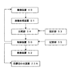
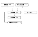
図1は第1、第2実施形態の基板貼り合わせ装置を示す模式図、図2は第1、第2実施形態の制御ブロック図、図3は第3実施形態の基板貼り合わせ装置を示す模式図、図4は第3実施形態の制御ブロック図である。
【0024】
(第1実施形態)(図1、図2)
基板貼り合わせ装置10は、上ガラス基板1と下ガラス基板2の間で、接着剤(シール剤)に囲まれる領域に液晶を充填したものを前工程から受入れ、この上ガラス基板1と下ガラス基板2を位置合わせした状態で貼り合わせ、セル(液晶表示パネル)を製造する。
【0025】
基板貼り合わせ装置10は、図1に示す如く、密閉容器11と、上ステージ21と、下ステージ22と、圧力調整装置30と、撮像装置40とを有する。
【0026】
密閉容器11は上ステージ21と下ステージ22を包囲し、前工程から搬送されてくる上ガラス基板1と下ガラス基板2をシャッター12から導入する。
【0027】
上ステージ21は上ガラス基板1を保持可能とし、上ステージ移動手段21Aにより昇降動する。
【0028】
下ステージ22は下ガラス基板2を保持可能とし、下ステージ移動手段22Aにより水平動、旋回動、昇降動する。
【0029】
圧力調整装置30は、密閉容器11の内部の圧力を調整するもので、例えば、真空源と気体供給源を有してなり、真空源を用いて密閉容器11内雰囲気を真空状態に減圧し、気体供給源を用いて真空状態とされた密閉容器11内雰囲気を大気圧に昇圧させる。
【0030】
撮像装置40は上ガラス基板1と下ガラス基板2の四隅のそれぞれに付してある位置検出用マークを撮像するもので、密閉容器11の下方に、上ステージ21に保持される上ガラス基板1及び下ステージ22に保持される下ガラス基板2の四隅に対応して1つずつ配置される。また、撮像装置40に対応して、密閉容器11にはのぞき窓11Aが、下ステージ22には貫通孔22Bがそれぞれ設けられ、撮像装置40は、これらののぞき窓11A及び貫通孔22Bを通して上ガラス基板1と下ガラス基板2の位置検出用マークを撮像する。尚、位置検出用マークは上ガラス基板1と下ガラス基板2の互いに向き合う互いの貼り合わせ面上に付される。撮像装置40はカメラ移動手段40Aにより昇降動する。
【0031】
従って、基板貼り合わせ装置10による上ガラス基板1と下ガラス基板2の貼り合わせ動作は例えば以下の通りになる。先ず、上ガラス基板1と下ガラス基板2をそれぞれ上ステージ21と下ステージ22に保持した状態で、圧力調整装置30により密閉容器11の内部を真空状態に減圧する。そして、撮像装置40により上ガラス基板1と下ガラス基板2の位置合わせマークを読取り、結果として上ガラス基板1と下ガラス基板2の両方向での相対位置ずれ状態を検出し、この相対位置ずれを修正するように下ステージ移動手段22A(位置合わせ装置)を制御し、上ステージ21と下ステージ22を基板1、2の面方向で相対移動させ、上ガラス基板1と下ガラス基板2を位置合わせする。上ステージ移動手段21Aにより上ステージ21を下降させ、圧力調整装置30による減圧下で上ガラス基板1と下ガラス基板2を接着剤を介して貼り合わせする。減圧下での貼り合わせにより、予め下ガラス基板2上に供給されている液晶中への空気の混入を回避できる。
【0032】
圧力調整装置30により密閉容器11の内部を大気圧に昇圧させるとともに、必要により撮像装置40と下ステージ移動手段22Aを用いて上ガラス基板1と下ガラス基板2を再位置合わせした後、上ステージ21と下ステージ22による上ガラス基板1と下ガラス基板2の保持を解除し、貼り合わせた上ガラス基板1と下ガラス基板2(セル)を密閉容器11から取出す。
【0033】
しかるに、基板貼り合わせ装置10は、図2に示す如く、上ガラス基板1と下ガラス基板2の上述した位置合わせを行なうに際し、上ガラス基板1と下ガラス基板2の位置検出用マークを撮像装置40により確実に撮像可能にするため、制御装置50、画像処理装置51、移動装置52、設定部53、比較部54、記憶部55を有する。
【0034】
画像処理装置51は、撮像装置40により撮像した上ガラス基板1と下ガラス基板2の位置検出用マークについて、撮像したマークパターンと設定された基準マークパターンとの一致度(以下、単に「一致度」ということがある。)を算出する。
【0035】
移動装置52は、上ステージ21の上ステージ移動手段21A、撮像装置40のカメラ移動手段40A等からなり、撮像装置40と上ステージ21又は下ステージ22との相対位置を調整し、結果として撮像装置40と上ガラス基板1又は下ガラス基板2との相対間隔を変化させる。
【0036】
設定部53は、撮像装置40と上ガラス基板1、下ガラス基板2の相対間隔の良否(撮像装置40の焦点深度内に基板1、2の位置検出用マークが入る状態か否か)を判定するための一致度に関する許容値を設定する。
【0037】
比較部54は、画像処理装置51が算出した一致度と、設定部53に設定された許容値とを比較する。
【0038】
記憶部55は、撮像装置40と上ガラス基板1、下ガラス基板2の相対間隔を変化させるときの相対間隔変化量とその相対間隔変化方向等の条件を設定してある。具体的には例えば、上ガラス基板1に関して、移動量d、駆動させる移動装置(本実施形態では上ステージ移動手段21A)及び初回修正時の移動方向(上、下の別で本実施形態では「下」)が設定されており、上ガラス基板1に関して、撮像したマークパターンの一致度が許容値を外れていた場合には、上ステージ21を下方向に設定された移動量dで移動させる、という具合である。尚、2回目以降の移動方向は、最初に算出された一致度と、相対間隔修正後に算出された一致度との比較に基づいて決定するものとし、一致度が増加していれば前回修正時と同方向へ、減少していれば、逆方向へ移動させる。尚、下ガラス基板2に関しても同じ要領で条件が設定されている。また、記憶部55は、撮像装置40と基板1、2の良好な相対間隔を求めるために、撮像装置40に許容される繰り返し撮像回数(以下、「許容回数」という。)を設定してある。
【0039】
制御装置50は、比較部54の比較結果を得て、画像処理装置51が算出した一致度が設定された許容値から外れていたことを条件に移動装置52を制御し、撮像装置40と上ガラス基板1、下ガラス基板2の相対間隔を予め記憶部55に定めた設定量だけ変化させる。そして、制御装置50は、上ガラス基板1、下ガラス基板2の位置検出用マークを撮像装置40により再度撮像し、撮像したマークパターンと基準マークパターンとの一致度を画像処理装置51により再度算出する。
【0040】
従って、制御装置50による上ガラス基板1と下ガラス基板2の位置合わせ手順は以下の如くなされる。尚、ここでは先ず、下ステージ22に保持される下ガラス基板2に付された位置検出用マークは撮像装置40の焦点深度内にあるものとし、上ステージ21に保持される上ガラス基板1の位置検出用マークのみが、撮像装置40の焦点深度から外れている場合について説明する。
【0041】
(1)撮像装置40により上ガラス基板1、下ガラス基板2の位置検出用マークを同時に撮像する。
【0042】
(2)画像処理装置51により、上ガラス基板1について撮像したマークパターンと設定された基準マークパターンの一致度を算出する。そして、画像処理装置51が算出した一致度と、設定部53に設定された許容値とを、比較部54で比較する。比較部54の比較結果が良(一致度が許容値の範囲内に入る)であれば、(5)ヘ移り、否であれば(3)へ移る。
【0043】
(3)撮像装置40による撮像回数が記憶部55に設定された許容回数を越えたか否か判別する。越えていないならば(4)ヘ移り、越えているならば位置合わせ不可のオペレータコール処理を行なう。
【0044】
(4)記憶部55の設定データを用い、移動装置52を制御する。
(4-1)移動装置52により撮像装置40と上ステージ21との相対位置を調整し、撮像装置40と上ガラス基板1との相対間隔を記憶部55に予め定めた設定量だけ変化させる。先の例では上ステージ21を撮像装置40に近づく方向に移動量dだけ変化させる。
【0045】
(4-2)上述(4-1)による相対間隔変化後に、上ガラス基板1、下ガラス基板2の位置検出用マークを再度撮像し、上ガラス基板1について撮像したマークパターンの一致度を画像処理装置51により再度算出する。
【0046】
(4-3)上述(4-2)で再度算出した一致度が前回算出分の一致度より増加し、比較部54の比較結果が良であれば(5)へ移る。一致度は増加したものの、比較結果が否であれば、移動装置52により、上ガラス基板1を撮像装置40に更に近づく方向に移動量dずつ相対間隔を変化させ、その都度、画像処理装置51による一致度の算出、比較部54による比較を許容回数内において比較結果が良となるまで繰り返す。比較部54による比較結果が良になれば、(5)へ移る。
【0047】
(4-4)上述(4-2)で再度算出した一致度が前回算出分の一致度から低減し、比較部54の比較結果が否であるときには、移動装置52により、上ステージ21を撮像装置40から遠くなる方向に移動量dずつ相対間隔を変化させ、その都度、画像処理装置51による一致度の算出、比較部54による比較を許容回数内において比較結果が良となるまで繰り返す。比較部54による比較結果が良になれば、(5)へ移る。
【0048】
(5)撮像装置40が撮像した上ガラス基板1、下ガラス基板2の位置検出用マークの画像データに基づき、前述した如く、上ガラス基板1と下ガラス基板2の面方向での相対位置ずれ状態を検出し、この相対位置ずれを修正するように下ステージ移動手段22Aを制御し、上ステージ21と下ステージ22を基板1、2の面方向で相対移動させ、上ガラス基板1と下ガラス基板2を位置合わせする。
【0049】
尚、上記第1実施形態において、便宜上、下ステージ22に保持される下ガラス基板2の位置検出用マークが常に撮像装置40の焦点深度内に入る例で説明したが、例えば、上下のガラス基板1、2の位置検出用マークがいずれも撮像装置40の焦点深度から外れる可能性を有する場合には、下記の如くに対応可能である。
【0050】
即ち、両基板1、2の撮像されたマークパターンの一致度が共に許容値から外れた場合でも、このような場合の基板1、2と撮像装置40の相対間隔を調整するための条件を記憶部55に設定しておくことで対応することが可能である。具体的には例えば、まず、上述した手順(1)〜(4)に沿って、上ガラス基板1におけるマークパターンの一致度が許容値内となるように、上ステージ移動手段21Aを移動量dで制御し、この後、同じく手順(2)〜(4)をたどって下ガラス基板2におけるマークパターンの一致度が許容値内となるように、下ステージ移動手段22Aを移動量dで制御する。尚、両基板1、2の撮像されたマークパターンの一致度が共に許容値から外れる場合は、上ガラス基板1に付された位置検出用マークが撮像装置40の焦点深度に対して上方側に外れ、また下ガラス基板2に付された位置検出用マークが撮像装置40の焦点深度に対して下方側に外れていることが考えられるので、移動手段21A、22Aによる上下ステージ21、22の最初の移動方向は、両ステージ21、22の相対間隔を狭める方向に設定すると良い。
【0051】
また、撮像装置40を昇降動させることで、撮像装置40と上下のガラス基板1、2の相対間隔を調整するものであっても良い。即ち、予め記憶部55には、例えば、上ガラス基板1に関して、カメラ移動手段40Aによって撮像装置40を移動量dで上方向に移動させるという条件を、下ガラス基板2に関して、移動量dで撮像装置40を下方向に移動させるという条件を設定しておく。そして、上述の(2)の工程では、上下のガラス基板1、2それぞれについて撮像したマークパターンの一致度を算出し、この結果、上ガラス基板1の撮像されたマークパターンの一致度のみが許容値から外れた場合には、記憶部55に設定された上ガラス基板1に対応する条件で、基板1、2と撮像装置40の相対間隔を調整する。また、下ガラス基板2の撮像されたマークパターンの一致度のみが許容値から外れた場合には、記憶部55に記憶された下ガラス基板2に対応する条件で、基板1、2と撮像装置40の相対間隔を調整する。また、両基板1、2の撮像されたマークパターンの一致度が共に許容値から外れた場合には、位置合わせ不可と判断しオペレータコール処理を行なう。
【0052】
本実施形態によれば以下の作用がある。
▲1▼上下のガラス基板1、2の位置検出用マークを撮像し、撮像したマークパターンと設定された基準マークパターンとの一致度を算出し、この算出した一致度に基づいて撮像装置40と上ガラス基板1、下ガラス基板2との相対間隔を変化させるものであり、上下のガラス基板1、2の位置検出用マークを撮像装置40の焦点深度内に確実に入れることができる。
【0053】
▲2▼上述▲1▼において、一致度に関する許容値を設定しており、算出した一致度が設定された許容値から外れていたときに、上下のガラス基板1、2と撮像装置40との相対間隔を予め定めた設定量だけ変化させるものであり、上下のガラス基板1、2の位置検出用マークを撮像装置40の焦点深度内により確実かつ効率的に入れることができる。
【0054】
(第2実施形態)(図1、図2)
第2実施形態の基板貼り合わせ装置10も、上ガラス基板1と下ガラス基板2の位置検出用マークを撮像装置40により確実に撮像するため、第1実施形態におけると同様に、制御装置50、画像処理装置51、移動装置52、設定部53、比較部54、記憶部55を有する。
【0055】
第2実施形態が第1実施形態と異なる点は、記憶部55が、上ガラス基板1、下ガラス基板2と撮像装置40との各相対間隔とそれに対応する一致度との関係を表すデータを記憶していることにある。制御装置50は、記憶部55に記憶されたデータに基づいて、移動装置52による基板1、2と撮像装置40との相対間隔変化量を設定する。尚、相対間隔と一致度との関係を表すデータは、例えば、実験により求めることが可能である。即ち、基板1、2と撮像装置40の相対間隔を一定距離ずつ変化させ、それぞれの相対間隔においてマークパターンの一致度を測定したデータを作成する。そして、このデータに基づいて相対間隔と一致度との関係を表す近似式を求め、この近似式を相対間隔と一致度との関係を表すデータとして用いる。
【0056】
従って、第2実施形態において、制御装置50による上ガラス基板1と下ガラス基板2の位置合わせ手順は以下の如くなされる。尚、本実施形態でも第1実施形態と同様に、下ステージ22に保持される下ガラス基板2の位置検出用マークは撮像装置40の焦点深度内にあるものと仮定して説明する。
【0057】
(1)撮像装置40により上ガラス基板1、下ガラス基板2の位置検出用マークを同時に撮像する。
【0058】
(2)画像処理装置51により、上ガラス基板1について撮像したマークパターンと設定された基準マークパターンの一致度を算出する。そして、画像処理装置51が算出した一致度と、設定部53に設定された許容値とを、比較部54で比較する。比較部54の比較結果が良(一致度が許容値の範囲内に入る)であれば、(5)ヘ移り、否であれば(3)へ移る。
【0059】
(3)撮像装置40による撮像回数が記憶部55に設定された許容回数を越えたか否か判別する。越えていないならば(4)ヘ移り、越えているならば位置合わせ不可のオペレータコール処理を行なう。
【0060】
(4)記憶部55の記憶データを用い、移動装置52を制御する。
(4-1)記憶部55の記憶データである、上ガラス基板1と撮像装置40との相対間隔と、それに対応する一致度との関係を表すデータを用いる。上述(2)で画像処理装置51が算出した一致度を上記データに参照し、上ガラス基板1と撮像装置40との現在の相対間隔を推測する。
【0061】
(4-2)画像処理装置51が算出する一致度が許容値に入るときの、上ガラス基板1と撮像装置40との目標とすべき相対間隔を記憶部55の上述(4)のデータから推測する。上述(4-1)の現在の相対間隔が目標とすべき相対間隔に入るように、移動装置52により撮像装置40と上ステージ21との相対位置を調整し、撮像装置40と上ガラス基板1との相対間隔を変化させ、前述(1)へ戻る。
【0062】
(5)撮像装置40が撮像した上ガラス基板1、下ガラス基板2の位置検出用マークの画像データに基づき、前述した如く、上ガラス基板1と下ガラス基板2の面方向での相対位置ずれ状態を検出し、この相対位置ずれを修正するように下ステージ移動手段22Aを制御し、上ステージ21と下ステージ22を基板1、2の面方向で相対移動させ、上ガラス基板1と下ガラス基板2を位置合わせする。
【0063】
本実施形態によれば、上下のガラス基板1、2と撮像装置40との各相対間隔とそれに対応する一致度との関係を表すデータを記憶しており、算出した一致度の設定された許容値に対する外れ分に応じた、上ガラス基板1と撮像装置40の相対間隔変化量を直ちに把握でき、上ガラス基板1の位置検出用マークを撮像装置40の焦点深度内に確実かつより効率的に入れることができる。
【0064】
尚、この第2実施形態においては、記憶部55に、上下のガラス基板1、2と撮像装置40との各相対間隔とそれに対応する一致度との関係を示すデータを記憶しておくものであったが、このデータに代えて、画像処理装置51が算出した各一致度に対応する撮像装置40と上下のガラス基板1、2との相対間隔の調整量を記憶しておくものであっても良い。この場合、第2実施形態における手順(4)において、画像処理装置51が一致度を算出すると、制御装置50は、記憶部55のデータから、撮像装置40と上(下)のガラス基板1(2)との相対間隔の調整量を求め、その求めた調整量分だけ撮像装置40と上下のガラス基板1、2との相対間隔を変化させることになる。
【0065】
(第3実施形態)(図3、図4)
第3実施形態の基板貼り合わせ装置10は、上ガラス基板1と下ガラス基板2の位置検出用マークを撮像装置40により確実に撮像するため、図3、図4に示す如く、制御装置60、厚み測定装置61、移動装置62、設定部63を有する。
【0066】
厚み測定装置61は、上下のガラス基板1、2の厚みT1、T2を測定する。厚み測定装置61は例えば基板1、2の密閉容器11への導入経路に沿う位置に導入経路に沿って搬送される基板1、2を上下から挟む如くに対向して設置された一対のセンサを有してなる。このセンサとしては、例えば、反射型の超音波センサを用いることができ、この一対のセンサ間を基板1、2が通過したときの各センサからの出力値と一対のセンサの配置間隔とに基づいて基板1、2の厚みT1、T2を測定する。そして、本実施形態においては、1枚の基板の板厚は均一であると仮定して基板1、2の略中央部で厚みを測定するものとするが、一枚の基板上で板厚にばらつき有する可能性がある場合には、基板1、2上の位置検出用マークに対応する部位それぞれの厚みを測定し、それらの平均値を用いる等しても良い。尚、センサは非接触式に限らず接触式のセンサ等、基板1、2の厚みを測定可能なセンサであれば他のものを用いることも可能である。
【0067】
移動装置62は、上ステージ21の上ステージ移動手段21A、撮像装置40のカメラ移動手段40A等からなり、撮像装置40と上ステージ21又は下ステージ22との相対位置を調整し、結果として撮像装置40と基板1、2との相対間隔を変化させる。
【0068】
設定部63は、撮像装置40と上ガラス基板1又は下ガラス基板2の位置検出用マークが付された貼り合わせ面との目標とすべき相対間隔M(撮像装置40の焦点距離)と、両基板1、2の貼り合わせ前の最も近接させ得る設定間隔Bとが設定される。
【0069】
制御装置60は、厚み測定装置61の測定結果に基づいて移動装置62を制御する。具体的には、移動装置62により、上下のステージ21、22間隔の中央位置と撮像装置40との間の距離が、設定部63に設定された目標相対間隔Mになるように、撮像装置40と上ステージ21又は下ステージ22との相対位置を調整する。また、移動装置62により、両基板1、2の位置検出用マークが付された貼り合わせ面の間隔が予め定めた設定間隔Bになるように、撮像装置40と上ステージ21又は下ステージ22との相対位置を調整する。このとき、上ステージ21と下ステージ22の相対間隔Aは、A=B+T1+T2である。
【0070】
従って、制御装置60による上ガラス基板1と下ガラス基板2の位置合わせ手順は以下の如くなされる。
【0071】
(1)厚み測定装置61により上ガラス基板1、下ガラス基板2の厚みT1、T2を測定する。
【0072】
(2) 測定した基板1、2の厚みT1、T2に基づいて上下のステージ21、22の相対間隔Aを算出する。そして、上下のステージ21、22の間隔が相対間隔Aとなるように、即ち、両基板1、2の位置検出用マークが付された貼り合わせ面の間隔が設定間隔Bとなるように、かつ、上下のステージ21、22間隔の中央位置と撮像装置40との間の距離が目標とする相対間隔M(撮像装置40の焦点距離)となるように、移動装置62を制御する。これにより、上下の基板1、2の位置検出用マークは、撮像装置40の焦点深度内に配置される。
【0073】
(3)上述(2)により、撮像装置40と上ガラス基板1と下ガラス基板2の相対位置を調整した状態で、撮像装置40により基板1、2の位置検出用マークを同時に撮像する。そして、撮像装置40が撮像した基板1、2の位置検出用マークの画像データに基づき、前述した如く、上ガラス基板1と下ガラス基板2の面方向での相対位置ずれ状態を検出し、この相対位置ずれを修正するように下ステージ移動手段22Aを制御し、上ステージ21と下ステージ22を基板1、2の面方向で相対移動させ、上ガラス基板1と下ガラス基板2を位置合わせする。
【0074】
本実施形態によれば以下の作用がある。
▲1▼上ガラス基板1と下ガラス基板2の測定厚みに基づいて、撮像装置40と上下のガラス基板1、2との相対間隔を調整するものであり、上下のガラス基板1、2の位置検出用マークを撮像装置40の焦点深度内に確実に入れることができる。
【0075】
▲2▼上述▲1▼において、測定された上下のガラス基板1、2の厚みに基づいて、両ガラス基板1、2の間隔が予め定めた値となるように、撮像装置40と上下のガラス基板1、2との相対間隔を調整するものであり、上下のガラス基板1、2の位置検出用マークを撮像装置40の焦点深度内により確実かつ効率的に入れることができる。
【0076】
尚、第3実施形態の手順(2)において、撮像装置40の焦点深度と設定間隔Bとの関係が、焦点深度<設定間隔Bである場合には、上下の基板1、2の位置検出用マークの良好な撮像画像を同時に撮像装置40で取り込むことはできないが、各基板1、2の位置検出用マークを個別に撮像装置40で撮像する等にて対応することが可能である。具体的には例えば、いずれか一方の基板の厚みの測定結果に基づいて撮像装置40と一方の基板の位置検出用マークが付された面との間の距離が目標とする相対間隔(撮像装置40の焦点距離)となるように、撮像装置40を上下に移動させ、この状態で位置検出用マークの位置を検出する。次に、他方の基板の厚みの測定結果に基づいて撮像装置40と他方の基板の位置検出用マークが付された面との間の距離が目標とする相対間隔(撮像装置40の焦点距離)となるように、撮像装置40を上下に移動させ、この状態で位置検出用マークの位置を検出する。撮像装置40は、同じ焦点深度内であっても焦点位置が最も鮮明な画像を得られると考えられるので、このようにすることで、位置検出精度が向上するという更なる効果を得ることができる。
【0077】
以上、本発明の実施の形態を図面により詳述したが、本発明の具体的な構成はこの実施の形態に限られるものではなく、本発明の要旨を逸脱しない範囲の設計の変更等があっても本発明に含まれる。例えば、本発明は単一の基板に付された位置検出用マークを検出する装置においても採用できる。
【0078】
また、上記第1、第2実施形態において、上ガラス基板1の位置検出用マークと下ガラス基板2の位置検出用マークとを撮像装置40の焦点深度内に同時に位置付ける例で説明したが、個別に位置付けるようにしても良い。具体的には例えば、設定部53に設定する撮像されたマークパターンと設定された基準マークパターンとの一致度に関する許容値を、両基板1、2の位置検出用マークを撮像装置40の焦点深度内に同時に位置付ける場合に比べて高い値、例えば、一致度100%或いはそれに近い値に設定する。そして、この許容値に基づき、第1、第2実施形態における工程(1)〜(5)にしたがって各基板1、2の位置検出用マークを撮像装置40で個別に撮像しその位置を検出する。このようにすることで、より精度の高いマーク位置検出を行なうことができるので、位置検出精度が向上するという更なる効果を得ることができる。
【0079】
また、接着剤は、シール性を有する接着剤に限らずシール性を有さない接着剤を用いることも可能である。
【0080】
また、基板は、液晶表示パネルを構成するガラス基板に限らず、プリント基板等であっても良い。
【0081】
【発明の効果】
以上のように本発明によれば、基板の位置検出用マークを撮像装置により確実に撮像することができる。また、これにより、基板貼り合わせの稼動率低下を防止することができる。
【図面の簡単な説明】
【図1】 図1は第1、第2実施形態の基板貼り合わせ装置を示す模式図である。
【図2】 図2は第1、第2実施形態の制御ブロック図である。
【図3】 図3は第3実施形態の基板貼り合わせ装置を示す模式図である。
【図4】 図4は第3実施形態の制御ブロック図である。
【符号の説明】
1 上ガラス基板(上基板)
2 下ガラス基板(下基板)
10 基板貼り合わせ装置
21 上ステージ
22 下ステージ
40 撮像装置
50 制御装置
51 画像処理装置
52 移動装置
53 設定部
54 比較部
55 記憶部
60 制御装置
61 厚み測定装置
62 移動装置
63 設定部[0001]
BACKGROUND OF THE INVENTION
The present inventionLCD panelThe present invention relates to a substrate bonding apparatus and method and a substrate detection apparatus suitable for use in the manufacture of manufacturing.
[0002]
[Prior art]
The substrate laminating apparatus has an upper stage for holding an upper glass substrate and a lower stage for holding a lower glass substrate, as described in JP-A-2000-66163, and includes an upper glass substrate and a lower glass substrate. It is supposed to be pasted in the aligned state.
[0003]
In the prior art, in order to align the upper glass substrate and the lower glass substrate, the position detection marks of the upper glass substrate and the lower glass substrate are imaged by an imaging device, and the upper glass substrate and the lower glass substrate are detected based on the captured image. The relative position shift state is detected, and the upper stage and the lower stage are relatively moved in the surface direction of the substrate so as to correct the relative position shift between the upper glass substrate and the lower glass substrate based on the detection result.
[0004]
[Problems to be solved by the invention]
However, in the prior art, when imaging the position detection marks of the upper glass substrate and the lower glass substrate with the imaging device, there is an error in the plate thickness of the upper glass substrate and the lower glass substrate. The position detection marks cannot be placed within the depth of focus of the imaging device placed at a fixed position, and the relative displacement between the upper glass substrate and the lower glass substrate cannot be detected based on the image data captured by the imaging device. May be. As a result, the substrates cannot be bonded, and the operation rate of the substrate bonding apparatus decreases.
[0005]
An object of the present invention is to reliably capture an image of a position detection mark on a substrate using an imaging device. This is also to prevent a reduction in the operation rate of the substrate bonding.
[0006]
[Means for Solving the Problems]
The invention of
[0007]
The invention of
[0008]
The invention of claim 3 further includes a setting unit that sets an allowable value related to the degree of coincidence in the invention of
[0009]
The invention of claim 4 is the invention of
[0010]
The invention according to claim 5 is a substrate bonding method in which the upper substrate held on the upper stage and the lower substrate held on the lower stage are aligned, and the position detection marks on the upper and lower substrates are attached.Simultaneously from the opposite direction with respect to the surface with the position detection markBased on the step of imaging, the step of calculating the degree of coincidence between the imaged mark pattern and the set reference mark pattern, and the calculated degree of coincidence,In the opposing direction of the imaging device and the upper and lower substrates so that the position detection marks of the upper and lower substrates are within the depth of focus of the imaging device.And a step of changing the relative interval.
[0011]
According to a sixth aspect of the present invention, in the fifth aspect of the invention, an allowable value related to the degree of coincidence is set, the calculated degree of coincidence is compared with the set allowable value, and the calculated degree of coincidence is set as a result of the comparison. Between the imaging device and the boardIn the opposite directionThe relative interval is changed by a predetermined amount, the substrate position detection mark is imaged again, and the degree of coincidence between the imaged mark pattern and the reference mark pattern is calculated again.
[0012]
The invention of claim 7 is a substrate laminating apparatus that has an upper stage for holding an upper substrate and a lower stage for holding a lower substrate, and bonds the upper substrate and the lower substrate in an aligned state, An imaging device that images a position detection mark on at least one of the upper and lower substrates, and the imaging device and at least one of the substratesIn a direction facing the surface to which the position detection mark is attachedA moving device that changes the relative distance, a thickness measuring device that measures the thickness of at least one of the substrates, and a control device that controls the moving device based on the measurement result of the thickness measuring device are provided.
[0013]
According to an eighth aspect of the present invention, in the seventh aspect of the present invention, the thickness measuring device further comprises the thicknesses of the upper and lower substrates.MeasurementThen, the control device is configured so that the distance between the two substrates becomes a predetermined value based on the measurement result of the thickness measuring device, and between the two substrates and the imaging device.In the opposite directionThe moving device is controlled so that the interval becomes a target relative interval.
[0014]
The invention according to claim 9 is a substrate bonding method in which the upper substrate held on the upper stage and the lower substrate held on the lower stage are bonded together, and the thickness of the held substrate is measured. And the relative distance between the imaging device and the at least one substrate based on the measured substrate thickness.In the direction facing the surface with the position detection mark on the substrateAnd a step of adjusting and a step of imaging the position detection mark on the at least one substrate.
[0015]
The invention according to
[0016]
The invention of claim 11Two pieces placed one above the otherA substrate detection device for detecting the position of a substrate,Up and downA mark for detecting the position of the boardSimultaneously from the opposite direction with respect to the surface with the position detection mark on the upper and lower substratesAn imaging device for imaging, and an imaging device;Up and downWith substrateIn the opposite directionA moving device for changing the relative spacing;SaidWith substrateSaidWith imaging deviceIn the opposite directionBased on the means for obtaining the data related to the relative interval and the data related to the relative intervalThe position detection marks of the upper and lower substrates are placed within the depth of focus of the imaging device.And a control device for controlling the moving device.
In the invention of
[0017]
[Action]
According to inventions of
(a)Obtaining data related to the relative distance between the substrate and the imaging device, and changing the relative distance between the imaging device and the substrate based on the data related to the relative distance,Up and downThe position detection mark of the substrate can be surely placed within the depth of focus of the imaging device.Up and downThe position detection mark on the substrate can be reliably imaged by the imaging device.
[0018]
According to inventions of
(b)The board position detection mark is imaged, the degree of coincidence between the imaged mark pattern and the set reference mark pattern is calculated, and the relative distance between the imaging device and the board is changed based on the calculated degree of coincidence. Yes,Up and downThe position detection mark of the substrate can be surely placed within the depth of focus of the imaging device.
[0019]
According to inventions of claims 3 and 6, the following(c)Action ofeffectThere is.
(c)Above(b)In this case, an allowable value for the degree of coincidence is set, and when the calculated degree of coincidence deviates from the set allowable value, the relative interval between the substrate and the imaging device is changed by a predetermined set amount. ,Up and downThe mark for detecting the position of the substrate can be inserted more reliably within the depth of focus of the imaging device.
[0020]
According to the invention of claim 4,(d)Action ofeffectThere is.
(d)Stores data representing the relationship between the relative distance between the substrate and the imaging device or the relative distance adjustment amount and the matching degree corresponding thereto, and immediately grasps the amount of change in the relative distance between the board and the imaging device from the calculated matching degree. CanUp and downThe position detection mark on the substrate can be reliably and efficiently placed within the depth of focus of the imaging device.
[0021]
According to the inventions of claims 7 and 9, the following(e)Action ofeffectThere is.
(e)The relative distance between the imaging device and the substrate is adjusted based on the measured thickness of the substrate, and the position detection mark on the substrate can be reliably placed within the depth of focus of the imaging device.
[0022]
According to the inventions of
(f)Above(e)In this case, the relative distance between the imaging device and the substrate is adjusted based on the measured thickness of the substrate so that the distance between the two substrates becomes a predetermined value, and the position detection marks on both the substrates are imaged. It can be reliably placed within the depth of focus of the device.
According to the invention of
(g) When the position detection mark on the lower substrate is within the depth of focus of the imaging device, the position detection mark on the upper substrate is imaged, and the degree of coincidence between the captured mark pattern and the set reference mark pattern is calculated. The relative distance between the imaging device and the upper substrate is changed based on the calculated degree of coincidence, and the position detection mark on the upper substrate can be reliably placed within the focal depth of the imaging device.
[0023]
DETAILED DESCRIPTION OF THE INVENTION
1 is the firstThe secondFIG. 2 is a schematic diagram showing a substrate bonding apparatus according to an embodiment.The secondFIG. 3 is a control block diagram of the embodiment.ThirdFIG. 4 is a schematic diagram showing a substrate bonding apparatus according to an embodiment.ThirdIt is a control block diagram of an embodiment.
[0024]
First Embodiment (FIGS. 1 and 2)
The
[0025]
As shown in FIG. 1, the
[0026]
The sealed
[0027]
The
[0028]
The
[0029]
The
[0030]
The
[0031]
Therefore, the bonding operation of the
[0032]
The inside of the sealed
[0033]
However, as shown in FIG. 2, the
[0034]
For the position detection marks of the
[0035]
The moving device 52 includes an upper
[0036]
The setting unit 53 determines whether the relative distance between the
[0037]
The comparison unit 54 compares the degree of coincidence calculated by the image processing device 51 with the allowable value set in the setting unit 53.
[0038]
The storage unit 55 sets conditions such as a relative interval change amount and a relative interval change direction when the relative interval between the
[0039]
The control device 50 obtains the comparison result of the comparison unit 54 and controls the moving device 52 on the condition that the degree of coincidence calculated by the image processing device 51 is out of the set allowable value. The relative distance between the
[0040]
Therefore, the alignment procedure of the
[0041]
(1) The position detection marks on the
[0042]
(2) The degree of coincidence between the mark pattern captured for the
[0043]
(3) It is determined whether or not the number of times of imaging by the
[0044]
(4) The moving device 52 is controlled using the setting data in the storage unit 55.
(4-1) The relative position between the
[0045]
(4-2) After the relative interval change according to (4-1) above, the position detection marks on the
[0046]
(4-3) If the degree of coincidence calculated again in the above (4-2) increases from the degree of coincidence for the previous calculation, and the comparison result of the comparison unit 54 is good, the process proceeds to (5). If the degree of coincidence increases, but the comparison result is negative, the moving device 52 changes the relative distance by the moving amount d in the direction in which the
[0047]
(4-4) When the degree of coincidence calculated again in the above (4-2) is reduced from the degree of coincidence for the previous calculation and the comparison result of the comparison unit 54 is negative, the moving device 52 images the
[0048]
(5) Based on the image data of the position detection marks of the
[0049]
In the first embodiment, for the sake of convenience, the position detection mark of the
[0050]
That is, even when the degree of coincidence between the imaged mark patterns of both the
[0051]
Further, the relative distance between the
[0052]
According to this embodiment, there are the following operations.
(1) The position detection marks on the upper and
[0053]
(2) In the above (1), an allowable value for the degree of coincidence is set, and when the calculated degree of coincidence deviates from the set allowable value, the upper and
[0054]
Second Embodiment (FIGS. 1 and 2)
Similarly to the first embodiment, the
[0055]
The second embodiment is different from the first embodiment in that the storage unit 55 stores data representing the relationship between the relative distances between the
[0056]
Therefore, in the second embodiment, the alignment procedure of the
[0057]
(1) The position detection marks on the
[0058]
(2) The degree of coincidence between the mark pattern captured for the
[0059]
(3) It is determined whether or not the number of times of imaging by the
[0060]
(4) The moving device 52 is controlled using the data stored in the storage unit 55.
(4-1) Data representing the relationship between the relative distance between the
[0061]
(4-2) The relative distance that should be the target between the
[0062]
(5) Based on the image data of the position detection marks of the
[0063]
According to the present embodiment, the data representing the relationship between the relative distance between the upper and
[0064]
In the second embodiment, the storage unit 55 stores data indicating the relationship between the relative distance between the upper and
[0065]
(Third Embodiment) (FIGS. 3 and 4)
Since the
[0066]
The
[0067]
The moving device 62 includes the upper stage moving means 21A of the
[0068]
The setting unit 63 includes a relative distance M (focal length of the imaging device 40) to be a target between the
[0069]
The control device 60 controls the moving device 62 based on the measurement result of the
[0070]
Therefore, the alignment procedure of the
[0071]
(1) The thicknesses T1 and T2 of the
[0072]
(2) The relative distance A between the upper and
[0073]
(3) The position detection marks on the
[0074]
According to this embodiment, there are the following operations.
(1) The relative distance between the
[0075]
(2) In the above (1), based on the measured thicknesses of the upper and
[0076]
In the procedure (2) of the third embodiment, when the relationship between the depth of focus of the
[0077]
Although the embodiment of the present invention has been described in detail with reference to the drawings, the specific configuration of the present invention is not limited to this embodiment, and there are design changes and the like without departing from the gist of the present invention. Is included in the present invention. For example, the present invention can be adopted in an apparatus for detecting a position detection mark attached to a single substrate.
[0078]
In the first and second embodiments, the position detection mark on the
[0079]
The adhesive is not limited to an adhesive having a sealing property, and an adhesive having no sealing property can also be used.
[0080]
Further, the substrate is not limited to the glass substrate constituting the liquid crystal display panel, and may be a printed board or the like.
[0081]
【The invention's effect】
As described above, according to the present invention, the position detection mark on the substrate can be reliably imaged by the imaging device. Moreover, this makes it possible to prevent a reduction in the operating rate of substrate bonding.
[Brief description of the drawings]
FIG. 1 shows the firstThe secondIt is a schematic diagram which shows the board | substrate bonding apparatus of embodiment.
FIG. 2 shows the firstThe secondIt is a control block diagram of an embodiment.
FIG. 3 showsThirdIt is a schematic diagram which shows the board | substrate bonding apparatus of embodiment.
FIG. 4 showsThirdIt is a control block diagram of an embodiment.
[Explanation of symbols]
1 Upper glass substrate (upper substrate)
2 Lower glass substrate (lower substrate)
10 Substrate bonding equipment
21 Upper stage
22 Lower stage
40 Imaging device
50 Control device
51 Image processing apparatus
52 Mobile device
53 Setting section
54 Comparison part
55 Memory unit
60 Control device
61 Thickness measuring device
62 Mobile device
63 Setting section
Claims (12)
上下の基板の位置検出用マークをその位置検出用マークが付された面に関して対向する方向から同時に撮像する撮像装置と、
撮像装置と前記上下の基板との前記対向する方向における相対間隔を変化させる移動装置と、
前記基板と前記撮像装置との前記対向する方向における相対間隔に係るデータを求める手段と、
相対間隔に係るデータに基づいて前記撮像装置の焦点深度内に前記上下の基板の位置検出用マークを入れるように前記移動装置を制御する制御装置とを有する基板貼り合わせ装置。A substrate laminating apparatus that has an upper stage that holds an upper substrate and a lower stage that holds a lower substrate, and bonds the upper substrate and the lower substrate in a state of alignment,
An imaging device for simultaneously imaging the position detection marks of the upper and lower substrates from the direction facing each other with respect to the surface with the position detection marks ;
A moving device that changes a relative distance between the imaging device and the upper and lower substrates in the facing direction ;
Means for obtaining data relating to a relative distance between the substrate and the imaging device in the facing direction ;
A substrate bonding apparatus comprising: a control device that controls the moving device so as to put the position detection marks of the upper and lower substrates within the focal depth of the imaging device based on data relating to a relative interval.
上下の基板の位置検出用マークをその位置検出用マークが付された面に関して対向する方向から同時に撮像する撮像装置と、
撮像装置と前記上下の基板との前記対向する方向における相対間隔を変化させる移動装置と、
撮像装置により得たマークパターンと設定された基準マークパターンとの一致度を算出する画像処理装置と、
算出した一致度に基づいて前記撮像装置の焦点深度内に前記上下の基板の位置検出用マークを入れるように前記移動装置を制御する制御装置とを有する基板貼り合わせ装置。A substrate laminating apparatus that has an upper stage that holds an upper substrate and a lower stage that holds a lower substrate, and bonds the upper substrate and the lower substrate in a state of alignment,
An imaging device for simultaneously imaging the position detection marks of the upper and lower substrates from the direction facing each other with respect to the surface with the position detection marks ;
A moving device that changes a relative distance between the imaging device and the upper and lower substrates in the facing direction ;
An image processing device for calculating the degree of coincidence between the mark pattern obtained by the imaging device and the set reference mark pattern;
A substrate bonding apparatus comprising: a control device that controls the moving device so as to put the position detection marks of the upper and lower substrates within the focal depth of the imaging device based on the calculated degree of coincidence.
算出した一致度と設定部に設定された許容値とを比較する比較部とを有し、
制御装置は、算出した一致度が設定された許容値から外れていたことを条件に移動装置を制御し、基板と撮像装置との前記対向する方向における相対間隔を予め定めた設定量だけ変化させる請求項2に記載の基板貼り合わせ装置。A setting unit for setting an allowable value for the degree of coincidence;
A comparison unit that compares the calculated degree of coincidence with the allowable value set in the setting unit;
The control device controls the moving device on the condition that the calculated degree of coincidence deviates from the set allowable value, and changes the relative distance between the substrate and the imaging device in the facing direction by a predetermined set amount. The substrate bonding apparatus according to claim 2.
制御装置は、記憶部に記憶されたデータに基づいて移動装置による基板と撮像装置との相対間隔変化量を設定する請求項2又は3に記載の基板貼り合わせ装置。A storage unit for storing data representing a relationship between a relative interval or a relative interval adjustment amount in the facing direction between the imaging device and the substrate imaged by the imaging device and a matching degree corresponding thereto;
The substrate bonding apparatus according to claim 2, wherein the control device sets a relative distance change amount between the substrate and the imaging device by the moving device based on data stored in the storage unit.
上下の基板の位置検出用マークをその位置検出用マークが付された面に関して対向する方向から同時に撮像する工程と、
撮像したマークパターンと設定された基準マークパターンとの一致度を算出する工程と、
算出した一致度に基づいて、前記撮像装置の焦点深度内に前記上下の基板の位置検出用マークが入るように前記撮像装置と前記上下の基板との前記対向する方向における相対間隔を変化させる工程とを有する基板貼り合わせ方法。A substrate laminating method for laminating an upper substrate held on an upper stage and a lower substrate held on a lower stage in an aligned state,
Simultaneously imaging the position detection marks of the upper and lower substrates from the opposite direction with respect to the surface with the position detection marks ;
Calculating the degree of coincidence between the captured mark pattern and the set reference mark pattern;
Based on the calculated degree of coincidence, a step of changing a relative distance between the imaging device and the upper and lower substrates in the facing direction so that the position detection marks of the upper and lower substrates are within the depth of focus of the imaging device. A substrate bonding method comprising:
基板の位置検出用マークを再度撮像し、撮像したマークパターンと基準マークパターンとの一致度を再度算出する請求項5に記載の基板貼り合わせ方法。Set the allowable values for the degree of coincidence, the calculated degree of matching is compared with the set allowable value, comparison of the results, said imaging device and the substrate when the calculated degree of coincidence is out from the set tolerance Change the relative spacing in the opposite direction by a preset amount,
6. The substrate bonding method according to claim 5, wherein the substrate position detection mark is imaged again, and the degree of coincidence between the imaged mark pattern and the reference mark pattern is calculated again.
上下の基板の少なくとも一方の基板の位置検出用マークを撮像する撮像装置と、
撮像装置と該少なくとも一方の基板との前記位置検出用マークが付された面に対向する方向における相対間隔を変化させる移動装置と、
該少なくとも一方の基板の厚みを測定する厚み測定装置と、
厚み測定装置の測定結果に基づいて移動装置を制御する制御装置とを有する基板貼り合わせ装置。A substrate laminating apparatus that has an upper stage that holds an upper substrate and a lower stage that holds a lower substrate, and bonds the upper substrate and the lower substrate in a state of alignment,
An imaging device for imaging a position detection mark on at least one of the upper and lower substrates;
A moving device that changes a relative distance between the imaging device and the at least one substrate in a direction facing the surface to which the position detection mark is attached ;
A thickness measuring device for measuring the thickness of the at least one substrate;
A substrate bonding apparatus comprising: a control device that controls the moving device based on a measurement result of the thickness measuring device.
保持される基板の厚みを測定する工程と、
測定された基板の厚みに基づいて撮像装置と該少なくとも一方の基板との相対間隔を前記基板における位置検出用マークが付された面に対向する方向において調整する工程と、
該少なくとも一方の基板の位置検出用マークを撮像する工程とを有する基板貼り合わせ方法。A substrate laminating method for laminating an upper substrate held on an upper stage and a lower substrate held on a lower stage in an aligned state,
Measuring the thickness of the substrate to be held;
Adjusting the relative distance between the imaging device and the at least one substrate based on the measured thickness of the substrate in a direction facing the surface on which the position detection mark is attached on the substrate ;
Imaging a position detection mark on at least one of the substrates.
前記上基板と前記下基板の厚みを測定する工程と、
測定された基板の厚みに基づいて、両基板の間隔が予め設定された値となるように、かつ前記両基板と前記撮像装置との間隔が前記基板における位置検出用マークが付された面に対向する方向において目標とする相対間隔となるように前記撮像装置と基板との前記対向する方向における相対間隔を調整する工程とを有する基板貼り合わせ方法。A substrate laminating method for laminating an upper substrate held on an upper stage and a lower substrate held on a lower stage in an aligned state,
Measuring the thickness of the upper substrate and the lower substrate;
Based on the measured thickness of the substrate, the distance between the two substrates becomes a preset value, and the distance between the two substrates and the imaging device is on the surface of the substrate with the position detection mark attached. substrate bonding method and a step of adjusting the relative spacing in opposite direction in the opposite direction between the imaging device and the substrate so that the relative spacing of the target.
上下の基板の位置検出用マークを前記上下の基板上において位置検出用マークが付された面に関して対向する方向から同時に撮像する撮像装置と、
撮像装置と上下の基板との前記対向する方向における相対間隔を変化させる移動装置と、
前記基板と前記撮像装置との前記対向する方向における相対間隔に係るデータを求める手段と、
相対間隔に係るデータに基づいて前記撮像装置の焦点深度内に前記上下の基板の位置検出用マークを入れるように前記移動装置を制御する制御装置とを有する基板検出装置。A substrate detection device for detecting the position of two substrates arranged above and below ,
An imaging device for imaging simultaneously from opposite directions with respect to the position detection mark in said upper and lower substrate position detecting mark of the upper and lower substrates is attached surface,
A moving device that changes a relative distance between the imaging device and the upper and lower substrates in the facing direction ;
Means for determining data relating to the relative distance in a direction the opposite of the substrate and the imaging device,
And a control device that controls the moving device so that the upper and lower substrate position detection marks are placed within the depth of focus of the imaging device based on data related to a relative interval.
撮像装置と前記上基板との前記対向する方向における相対間隔を変化させる移動装置と、A moving device that changes a relative distance between the imaging device and the upper substrate in the facing direction;
撮像装置により得た前記上基板におけるマークパターンと設定された基準マークパターンとの一致度を算出する画像処理装置と、An image processing device for calculating the degree of coincidence between the mark pattern on the upper substrate obtained by the imaging device and the set reference mark pattern;
算出した一致度に基づいて前記移動装置を制御する制御装置とを備え、A control device for controlling the mobile device based on the calculated degree of coincidence,
前記下ステージと前記撮像装置とは、前記下ステージに保持された前記下基板の位置検出用マークが前記撮像装置の焦点深度内に入れるように前記対向する方向における相対間隔が設定されており、The lower stage and the imaging device are set with a relative interval in the facing direction so that the position detection mark of the lower substrate held on the lower stage is within the depth of focus of the imaging device,
前記制御装置は、前記一致度に基づいて、前記撮像装置の焦点深度内に前記上基板の位置検出用マークを入れるように前記移動装置を制御することを特徴とする基板貼り合わせThe substrate bonding is characterized in that the control device controls the moving device so as to put a position detection mark of the upper substrate within a depth of focus of the imaging device based on the degree of coincidence. 装置。apparatus.
Priority Applications (5)
| Application Number | Priority Date | Filing Date | Title |
|---|---|---|---|
| JP2003025222A JP4038133B2 (en) | 2002-02-28 | 2003-01-31 | Substrate bonding apparatus and method, and substrate detection apparatus |
| US10/372,453 US20030159769A1 (en) | 2002-02-28 | 2003-02-24 | Substrate laminating apparatus and method thereof and substrate detecting apparatus |
| TW092104096A TWI320494B (en) | 2002-02-28 | 2003-02-26 | Substrate laminating apparatus and method thereof and substrate detecting apparatus |
| KR1020030011891A KR100706460B1 (en) | 2002-02-28 | 2003-02-26 | Substrate laminating apparatus and method thereof and substrate detecting apparatus |
| CNB031070027A CN1282007C (en) | 2002-02-28 | 2003-02-28 | Base board plying-up device and its method and base board detector |
Applications Claiming Priority (3)
| Application Number | Priority Date | Filing Date | Title |
|---|---|---|---|
| JP2002-55064 | 2002-02-28 | ||
| JP2002055064 | 2002-02-28 | ||
| JP2003025222A JP4038133B2 (en) | 2002-02-28 | 2003-01-31 | Substrate bonding apparatus and method, and substrate detection apparatus |
Publications (3)
| Publication Number | Publication Date |
|---|---|
| JP2003322834A JP2003322834A (en) | 2003-11-14 |
| JP2003322834A5 JP2003322834A5 (en) | 2005-08-04 |
| JP4038133B2 true JP4038133B2 (en) | 2008-01-23 |
Family
ID=27759722
Family Applications (1)
| Application Number | Title | Priority Date | Filing Date |
|---|---|---|---|
| JP2003025222A Expired - Fee Related JP4038133B2 (en) | 2002-02-28 | 2003-01-31 | Substrate bonding apparatus and method, and substrate detection apparatus |
Country Status (5)
| Country | Link |
|---|---|
| US (1) | US20030159769A1 (en) |
| JP (1) | JP4038133B2 (en) |
| KR (1) | KR100706460B1 (en) |
| CN (1) | CN1282007C (en) |
| TW (1) | TWI320494B (en) |
Families Citing this family (30)
| Publication number | Priority date | Publication date | Assignee | Title |
|---|---|---|---|---|
| KR100586787B1 (en) * | 2002-12-04 | 2006-06-08 | 시바우라 메카트로닉스 가부시키가이샤 | Method of bonding substrates and apparatus for bonding substrates |
| JP4585206B2 (en) * | 2003-03-04 | 2010-11-24 | 芝浦メカトロニクス株式会社 | Substrate bonding method and bonding apparatus |
| WO2005118440A1 (en) * | 2004-06-03 | 2005-12-15 | Unaxis Balzers Aktiengesellschaft | Table used to receive a workpiece and method for treating a workpiece on said type of table |
| JP2007101905A (en) * | 2005-10-04 | 2007-04-19 | Shibaura Mechatronics Corp | Substrate detection device and substrate detection method, and substrate bonding device and substrate bonding method using the substrate detection device and the substrate detection method |
| JP4941305B2 (en) * | 2005-10-12 | 2012-05-30 | 株式会社村田製作所 | Joining device |
| CN101326457B (en) | 2005-12-12 | 2010-11-17 | 株式会社村田制作所 | Aligning apparatus, bonding apparatus and aligning method |
| JP4361538B2 (en) * | 2006-02-16 | 2009-11-11 | 株式会社フューチャービジョン | Static elimination method for glass substrate |
| CN100495149C (en) * | 2006-08-17 | 2009-06-03 | 株式会社爱发科 | Joint method and manufacturing device for joint substrate |
| JP4728433B2 (en) * | 2008-01-25 | 2011-07-20 | パナソニック株式会社 | Inspection apparatus and inspection method |
| CN101957514B (en) * | 2010-08-30 | 2012-01-18 | 华映视讯(吴江)有限公司 | Panel assembly alignment system and alignment method thereof |
| CN102673090B (en) * | 2011-03-18 | 2015-01-14 | 宸鸿科技(厦门)有限公司 | Multilayer board bonding device and method |
| JP5791101B2 (en) * | 2011-05-16 | 2015-10-07 | 芝浦メカトロニクス株式会社 | Bonded plate inspection apparatus and method |
| JP5411905B2 (en) * | 2011-09-30 | 2014-02-12 | オリジン電気株式会社 | Joining member manufacturing apparatus and joining member manufacturing method |
| TWI454794B (en) * | 2011-11-11 | 2014-10-01 | Efun Technology Co Ltd | Film machine |
| CN102555408A (en) * | 2012-02-09 | 2012-07-11 | 华映视讯(吴江)有限公司 | Binding apparatus suitable for liquid crystal display panels |
| JP2013218198A (en) * | 2012-04-11 | 2013-10-24 | Hitachi High-Technologies Corp | Substrate lamination apparatus |
| CN102673095B (en) * | 2012-06-01 | 2014-09-03 | 深圳市华星光电技术有限公司 | Vacuum laminating machine applicable to all generations and operating method thereof |
| WO2014021192A1 (en) * | 2012-07-30 | 2014-02-06 | 芝浦メカトロニクス株式会社 | Substrate bonding apparatus and substrate bonding method |
| CN102902102B (en) * | 2012-10-30 | 2015-08-19 | 东莞市凯博美光电科技股份有限公司 | The applying method of 3D grating and bore hole 3D display screen in bore hole 3D display screen |
| CN102998833B (en) * | 2012-12-14 | 2015-05-13 | 京东方科技集团股份有限公司 | Array substrate and color film substrate box alignment method |
| SG11201505870TA (en) * | 2013-01-30 | 2015-08-28 | Origin Electric | Member bonding apparatus |
| JP6100570B2 (en) * | 2013-03-22 | 2017-03-22 | 株式会社東芝 | Display device manufacturing apparatus and display device manufacturing method |
| JP6100571B2 (en) | 2013-03-22 | 2017-03-22 | 株式会社東芝 | Display device manufacturing apparatus and display device manufacturing method |
| JP6311967B2 (en) * | 2014-03-06 | 2018-04-18 | Tianma Japan株式会社 | Substrate bonding apparatus and substrate bonding method |
| CN105511126B (en) * | 2016-01-21 | 2018-11-13 | 京东方科技集团股份有限公司 | Display panel and preparation method thereof and detection method |
| CN107238957A (en) * | 2017-08-02 | 2017-10-10 | 业成科技(成都)有限公司 | Abutted equipment and its applying method |
| CN109473365A (en) * | 2017-09-08 | 2019-03-15 | 李亚玲 | The measurement and monitoring method of the heavy film offset processing procedure exception of CVD |
| CN107639921A (en) * | 2017-09-21 | 2018-01-30 | 歌尔股份有限公司 | Laminating apparatus |
| CN110632775A (en) * | 2019-09-05 | 2019-12-31 | 东莞通华液晶有限公司 | Registering method for laminated glass substrate |
| CN114454591A (en) * | 2022-02-09 | 2022-05-10 | 创维集团智能装备有限公司 | Panel bonding method and device, electronic equipment and readable storage medium |
Family Cites Families (4)
| Publication number | Priority date | Publication date | Assignee | Title |
|---|---|---|---|---|
| US5499127A (en) * | 1992-05-25 | 1996-03-12 | Sharp Kabushiki Kaisha | Liquid crystal display device having a larger gap between the substrates in the display area than in the sealant area |
| US5407519A (en) * | 1993-07-07 | 1995-04-18 | Interserv Corp. | Apparatus for manufacturing liquid crystal display screens |
| JP3658110B2 (en) * | 1995-11-27 | 2005-06-08 | キヤノン株式会社 | Manufacturing method and manufacturing apparatus for image display device |
| KR100669096B1 (en) * | 2000-02-21 | 2007-01-16 | 엘지.필립스 엘시디 주식회사 | Glass Laminating Apparatus |
-
2003
- 2003-01-31 JP JP2003025222A patent/JP4038133B2/en not_active Expired - Fee Related
- 2003-02-24 US US10/372,453 patent/US20030159769A1/en not_active Abandoned
- 2003-02-26 TW TW092104096A patent/TWI320494B/en not_active IP Right Cessation
- 2003-02-26 KR KR1020030011891A patent/KR100706460B1/en not_active IP Right Cessation
- 2003-02-28 CN CNB031070027A patent/CN1282007C/en not_active Expired - Lifetime
Also Published As
| Publication number | Publication date |
|---|---|
| CN1441294A (en) | 2003-09-10 |
| US20030159769A1 (en) | 2003-08-28 |
| JP2003322834A (en) | 2003-11-14 |
| TW200304016A (en) | 2003-09-16 |
| CN1282007C (en) | 2006-10-25 |
| KR20030071519A (en) | 2003-09-03 |
| KR100706460B1 (en) | 2007-04-10 |
| TWI320494B (en) | 2010-02-11 |
Similar Documents
| Publication | Publication Date | Title |
|---|---|---|
| JP4038133B2 (en) | Substrate bonding apparatus and method, and substrate detection apparatus | |
| US6991825B2 (en) | Dispensation of controlled quantities of material onto a substrate | |
| CN101794721B (en) | Alignment apparatus for semiconductor wafer | |
| TWI417621B (en) | Substrate bonding device and substrate bonding method | |
| JP4628205B2 (en) | Feedback correction method and component mounting method | |
| JP2019039072A (en) | Alignment method and alignment device, and vacuum vapor deposition method and vacuum vapor deposition device including the same | |
| CN110918388B (en) | Dispensing device and dispensing method | |
| CN111742399A (en) | Contact accuracy assurance method, contact accuracy assurance mechanism, and inspection device | |
| JP5301363B2 (en) | Bonding device and bonding method | |
| CN110918389B (en) | Dispensing device and dispensing method | |
| KR20150061593A (en) | Applicator, application method, appratus and method for manufacturing a display device member | |
| JP5454310B2 (en) | Substrate bonding apparatus and substrate bonding method | |
| KR20150003161A (en) | Exposure writing device and exposure writing method | |
| TW201218246A (en) | characterized by detecting the positions of a mask and a work-piece alignment marks for several times to thereby check the difference between a first alignment measure and a second alignment measure | |
| JP7112341B2 (en) | Mounting equipment and mounting method | |
| US9435020B2 (en) | Thin film deposition apparatus and method of forming thin film using the same | |
| JP4100649B2 (en) | Chip bonding apparatus and calibration method therefor | |
| JP4100648B2 (en) | Chip bonding apparatus and calibration method therefor | |
| KR20090008114A (en) | Inspection apparatus and substrate processing system | |
| JP2008218488A (en) | Mounting method | |
| US20240120219A1 (en) | Bonding apparatus and bonding method | |
| KR102094962B1 (en) | Method for High Accuracy Aligning Substrates and Substrate Attaching Apparatus Using the Same Method | |
| KR100948805B1 (en) | Electromagnetic interference detecting apparatus, and controlling method | |
| JP2005340697A (en) | Method and equipment for packaging electronic component | |
| JP2020119970A (en) | Mounting device and mounting method |
Legal Events
| Date | Code | Title | Description |
|---|---|---|---|
| A521 | Request for written amendment filed |
Free format text: JAPANESE INTERMEDIATE CODE: A523 Effective date: 20041227 |
|
| A621 | Written request for application examination |
Free format text: JAPANESE INTERMEDIATE CODE: A621 Effective date: 20041227 |
|
| A977 | Report on retrieval |
Free format text: JAPANESE INTERMEDIATE CODE: A971007 Effective date: 20060703 |
|
| A131 | Notification of reasons for refusal |
Free format text: JAPANESE INTERMEDIATE CODE: A131 Effective date: 20070410 |
|
| A521 | Request for written amendment filed |
Free format text: JAPANESE INTERMEDIATE CODE: A523 Effective date: 20070605 |
|
| TRDD | Decision of grant or rejection written | ||
| A01 | Written decision to grant a patent or to grant a registration (utility model) |
Free format text: JAPANESE INTERMEDIATE CODE: A01 Effective date: 20071030 |
|
| A61 | First payment of annual fees (during grant procedure) |
Free format text: JAPANESE INTERMEDIATE CODE: A61 Effective date: 20071102 |
|
| R150 | Certificate of patent or registration of utility model |
Ref document number: 4038133 Country of ref document: JP Free format text: JAPANESE INTERMEDIATE CODE: R150 Free format text: JAPANESE INTERMEDIATE CODE: R150 |
|
| FPAY | Renewal fee payment (event date is renewal date of database) |
Free format text: PAYMENT UNTIL: 20101109 Year of fee payment: 3 |
|
| FPAY | Renewal fee payment (event date is renewal date of database) |
Free format text: PAYMENT UNTIL: 20111109 Year of fee payment: 4 |
|
| FPAY | Renewal fee payment (event date is renewal date of database) |
Free format text: PAYMENT UNTIL: 20111109 Year of fee payment: 4 |
|
| FPAY | Renewal fee payment (event date is renewal date of database) |
Free format text: PAYMENT UNTIL: 20121109 Year of fee payment: 5 |
|
| FPAY | Renewal fee payment (event date is renewal date of database) |
Free format text: PAYMENT UNTIL: 20131109 Year of fee payment: 6 |
|
| LAPS | Cancellation because of no payment of annual fees |