JP4017754B2 - Liquid crystal display device and manufacturing method thereof - Google Patents
Liquid crystal display device and manufacturing method thereof Download PDFInfo
- Publication number
- JP4017754B2 JP4017754B2 JP19201098A JP19201098A JP4017754B2 JP 4017754 B2 JP4017754 B2 JP 4017754B2 JP 19201098 A JP19201098 A JP 19201098A JP 19201098 A JP19201098 A JP 19201098A JP 4017754 B2 JP4017754 B2 JP 4017754B2
- Authority
- JP
- Japan
- Prior art keywords
- insulating film
- forming
- substrate
- liquid crystal
- region
- Prior art date
- Legal status (The legal status is an assumption and is not a legal conclusion. Google has not performed a legal analysis and makes no representation as to the accuracy of the status listed.)
- Expired - Fee Related
Links
- 239000004973 liquid crystal related substance Substances 0.000 title claims description 67
- 238000004519 manufacturing process Methods 0.000 title claims description 17
- 239000010408 film Substances 0.000 claims description 111
- 239000000758 substrate Substances 0.000 claims description 79
- 230000001681 protective effect Effects 0.000 claims description 59
- 239000010409 thin film Substances 0.000 claims description 30
- 239000004020 conductor Substances 0.000 claims description 22
- 239000000203 mixture Substances 0.000 claims description 20
- 239000004065 semiconductor Substances 0.000 claims description 20
- 238000000034 method Methods 0.000 claims description 17
- 239000011521 glass Substances 0.000 description 30
- 229910021417 amorphous silicon Inorganic materials 0.000 description 27
- 239000002245 particle Substances 0.000 description 14
- 238000010586 diagram Methods 0.000 description 8
- 230000006378 damage Effects 0.000 description 4
- 229910000583 Nd alloy Inorganic materials 0.000 description 3
- 229910000542 Sc alloy Inorganic materials 0.000 description 3
- 239000011159 matrix material Substances 0.000 description 3
- XUIMIQQOPSSXEZ-UHFFFAOYSA-N Silicon Chemical compound [Si] XUIMIQQOPSSXEZ-UHFFFAOYSA-N 0.000 description 2
- 230000015572 biosynthetic process Effects 0.000 description 2
- 239000012535 impurity Substances 0.000 description 2
- 238000000059 patterning Methods 0.000 description 2
- 229910052710 silicon Inorganic materials 0.000 description 2
- 239000010703 silicon Substances 0.000 description 2
- 230000008021 deposition Effects 0.000 description 1
- 230000000694 effects Effects 0.000 description 1
- 238000005530 etching Methods 0.000 description 1
- 230000010365 information processing Effects 0.000 description 1
- 238000009413 insulation Methods 0.000 description 1
- 238000010338 mechanical breakdown Methods 0.000 description 1
- 230000002093 peripheral effect Effects 0.000 description 1
- 125000006850 spacer group Chemical group 0.000 description 1
Images


Classifications
-
- G—PHYSICS
- G02—OPTICS
- G02F—OPTICAL DEVICES OR ARRANGEMENTS FOR THE CONTROL OF LIGHT BY MODIFICATION OF THE OPTICAL PROPERTIES OF THE MEDIA OF THE ELEMENTS INVOLVED THEREIN; NON-LINEAR OPTICS; FREQUENCY-CHANGING OF LIGHT; OPTICAL LOGIC ELEMENTS; OPTICAL ANALOGUE/DIGITAL CONVERTERS
- G02F1/00—Devices or arrangements for the control of the intensity, colour, phase, polarisation or direction of light arriving from an independent light source, e.g. switching, gating or modulating; Non-linear optics
- G02F1/01—Devices or arrangements for the control of the intensity, colour, phase, polarisation or direction of light arriving from an independent light source, e.g. switching, gating or modulating; Non-linear optics for the control of the intensity, phase, polarisation or colour
- G02F1/13—Devices or arrangements for the control of the intensity, colour, phase, polarisation or direction of light arriving from an independent light source, e.g. switching, gating or modulating; Non-linear optics for the control of the intensity, phase, polarisation or colour based on liquid crystals, e.g. single liquid crystal display cells
- G02F1/133—Constructional arrangements; Operation of liquid crystal cells; Circuit arrangements
- G02F1/1333—Constructional arrangements; Manufacturing methods
- G02F1/1345—Conductors connecting electrodes to cell terminals
- G02F1/13458—Terminal pads
-
- G—PHYSICS
- G02—OPTICS
- G02F—OPTICAL DEVICES OR ARRANGEMENTS FOR THE CONTROL OF LIGHT BY MODIFICATION OF THE OPTICAL PROPERTIES OF THE MEDIA OF THE ELEMENTS INVOLVED THEREIN; NON-LINEAR OPTICS; FREQUENCY-CHANGING OF LIGHT; OPTICAL LOGIC ELEMENTS; OPTICAL ANALOGUE/DIGITAL CONVERTERS
- G02F1/00—Devices or arrangements for the control of the intensity, colour, phase, polarisation or direction of light arriving from an independent light source, e.g. switching, gating or modulating; Non-linear optics
- G02F1/01—Devices or arrangements for the control of the intensity, colour, phase, polarisation or direction of light arriving from an independent light source, e.g. switching, gating or modulating; Non-linear optics for the control of the intensity, phase, polarisation or colour
- G02F1/13—Devices or arrangements for the control of the intensity, colour, phase, polarisation or direction of light arriving from an independent light source, e.g. switching, gating or modulating; Non-linear optics for the control of the intensity, phase, polarisation or colour based on liquid crystals, e.g. single liquid crystal display cells
- G02F1/133—Constructional arrangements; Operation of liquid crystal cells; Circuit arrangements
- G02F1/136—Liquid crystal cells structurally associated with a semi-conducting layer or substrate, e.g. cells forming part of an integrated circuit
- G02F1/1362—Active matrix addressed cells
-
- G—PHYSICS
- G02—OPTICS
- G02F—OPTICAL DEVICES OR ARRANGEMENTS FOR THE CONTROL OF LIGHT BY MODIFICATION OF THE OPTICAL PROPERTIES OF THE MEDIA OF THE ELEMENTS INVOLVED THEREIN; NON-LINEAR OPTICS; FREQUENCY-CHANGING OF LIGHT; OPTICAL LOGIC ELEMENTS; OPTICAL ANALOGUE/DIGITAL CONVERTERS
- G02F1/00—Devices or arrangements for the control of the intensity, colour, phase, polarisation or direction of light arriving from an independent light source, e.g. switching, gating or modulating; Non-linear optics
- G02F1/01—Devices or arrangements for the control of the intensity, colour, phase, polarisation or direction of light arriving from an independent light source, e.g. switching, gating or modulating; Non-linear optics for the control of the intensity, phase, polarisation or colour
- G02F1/13—Devices or arrangements for the control of the intensity, colour, phase, polarisation or direction of light arriving from an independent light source, e.g. switching, gating or modulating; Non-linear optics for the control of the intensity, phase, polarisation or colour based on liquid crystals, e.g. single liquid crystal display cells
- G02F1/133—Constructional arrangements; Operation of liquid crystal cells; Circuit arrangements
- G02F1/1333—Constructional arrangements; Manufacturing methods
- G02F1/1345—Conductors connecting electrodes to cell terminals
Landscapes
- Physics & Mathematics (AREA)
- Nonlinear Science (AREA)
- Mathematical Physics (AREA)
- Chemical & Material Sciences (AREA)
- Crystallography & Structural Chemistry (AREA)
- General Physics & Mathematics (AREA)
- Optics & Photonics (AREA)
- Engineering & Computer Science (AREA)
- Microelectronics & Electronic Packaging (AREA)
- Liquid Crystal (AREA)
- Devices For Indicating Variable Information By Combining Individual Elements (AREA)
- Thin Film Transistor (AREA)
Description
【0001】
【発明の属する技術分野】
本発明は、一般に液晶表示装置に関し、特に薄膜トランジスタ(TFT)を備えた液晶表示装置に関する。
液晶表示装置はコンピュータを初めとする情報処理装置において、小型で低消費電力の画像表示装置として広く使われている。
【0002】
特に、高品質のカラー表示を実現するため、液晶表示装置中の個々の画素電極を駆動する、いわゆるアクティブマトリクス駆動方式の液晶表示装置が広く使われている。かかるアクティブマトリクス駆動方式の液晶表示装置では、個々の画素電極をオンオフ制御するために、各々の画素電極に対応して、液晶パネルを構成するガラス基板上にTFTが設けられる。
【0003】
【従来の技術】
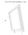
図1は、従来のアクティブマトリクス駆動型液晶表示装置10の構成を示す。
図1を参照するに、液晶表示装置10は多数のTFTおよびこれに協働する透明画素電極を担持するTFTガラス基板11と、前記TFT基板11上に形成された対向ガラス基板12とよりなり、基板11と12との間には液晶層1が、図示を省略したシール部材により封入されている。液晶表示装置10では、前記透明画素電極を、対向するTFTを介して選択的に駆動することにより、液晶層中において、前記選択された画素電極に対応して、液晶分子の配向を選択的に変化させる。さらに、前記ガラス基板11および12の外側には、それぞれ図示しないが偏光板が、直交ニコル状態で配設されている。また、ガラス基板11および12の内側には、液晶層に接するように分子配向膜が形成され、液晶分子の配向方向を規制する。
【0004】
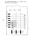
図2は前記TFTガラス基板11の一部を拡大して示す。
図2を参照するに、前記ガラス基板11上には、走査信号を供給される多数のパッド電極11Aおよびこれから延在する多数の走査電極11aと、画像信号を供給される多数のパッド電極11Bおよびこれから延在する多数の信号電極11bとが、走査電極11aの延在方向と走査電極11bの延在方向とが略直交するように形成されており、前記走査電極11aと前記信号電極11bとの交点には、TFT11Cが形成されている。さらに、前記基板11上には、各々のTFT11Cに対応して透明画素電極11Dが形成されており、各々のTFT11Cは対応する走査電極11a上の走査信号により選択され、対応する信号電極11b上の画像信号により、協働する透明画素電極11Dを駆動する。
【0005】
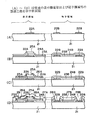
図3(A)〜(D)は、かかる従来の液晶表示装置の製造工程を示す断面図である。ただし、図3(A)〜(D)の各図中、左図はTFT11Cを含む表示領域を、また右図はパッド電極11A、11Bを含む端子領域を示す。
まず、図3(A)を参照するに、前記表示領域に対応して、前記TFT基板11に対応するガラス基板21上に、前記走査電極11aに接続されたAl−Nd合金あるいはAl−Sc合金パターン22Aが前記TFT部のゲート電極として形成される。同時に、前記ガラス基板21上の端子領域において、前記ガラス基板21上に、前記パッド電極11A、11Bに対応する端子電極22Bが、前記ゲート電極22Aと同じAl−Nd合金あるいはAl−Sc合金により形成される。
【0006】
次に、図3(B)の工程で、前記表示領域において、SiNよりなるゲート絶縁膜23Aを、前記ゲート電極22Aを覆うように堆積し、さらに前記ゲート絶縁膜23A上に、n- 型の不純物をドープしたアモルファスシリコン層24Aを堆積する。続いて、前記アモルファスシリコン層24A中、前記ゲート電極22A直上のチャネル領域に相当する部分に、SiNよりなるチャネル保護膜25Aをパターニング形成する。
【0007】
図3(B)の工程では、同時に右図の端子領域において、前記端子電極22Bを覆うように、前記SiNよりなる絶縁膜23Aと同一の厚さで、絶縁膜23Bを堆積し、さらに前記絶縁膜23Bの上層に、前記アモルファス・シリコン層24Aと同一の厚さでアモルファス・シリコン層24Bを形成する。
さらに、図3(C)に示す工程では、前記表示領域において、前記アモルファス・シリコン層24A上に、前記チャネル保護膜25Aの両側に隣接して、n+ 型アモルファスシリコンパターン26Aを形成し、それぞれによりTFTのソースおよびドレインを構成する。
【0008】
続いて、図3(D)の工程で、前記表示領域において、前記ゲート絶縁膜23A上に、前記n+ 型アモルファスシリコン層26Aと前記チャネル保護膜25Aとを覆うように、SiNよりなる保護膜27Aを堆積し、さらに前記保護膜27A中に、前記アモルファスシリコンパターン26Aの一方に対応してコンタクトホール28Aを形成する。さらに前記保護膜27A上にコンタクトホール28Aに対応して透明画素電極29を、前記コンタクトホール28Aを介して前記アモルファスシリコンパターン26Aにコンタクトするように形成する。透明画素電極29は、図2の透明画素電極11Dに対応する。
【0009】
一方、前記図3(D)左図の工程と同時に、同図右図に示す端子領域では、アモルファスシリコン層24B上に、前記保護膜27Aに対応する保護膜27Bを堆積し、これに前記端子電極22Bを露出するコンタクトホール28Bを形成する。図4に示すように、かかる液晶表示装置52では、前記端子領域のコンタクトホール28Bにおいて、表示パネル54中の前記端子電極22Bに駆動集積回路素子56がTABリード(図示せず)により接続される。
【0010】
以上の従来における液晶表示装置においては、図3(A)〜(D)の工程によって形成されたTFT基板21に対向ガラス基板を重ね合わせることによって液晶表示装置が構成される。
【0011】
【発明が解決しようとする課題】
ところで、かかる液晶表示装置を製造する場合においては、半導体集積回路チップの製造の場合と同様に製造コストを低減する必要性から、大面積のガラス基板上に、複数の前記液晶表示装置を隣接して製造し、製造後に前記大面積ガラス基板を個々の液晶表示装置に分割、切断することが一般になされている。前記切断後の一例として従来の液晶表示装置の断面図を図5に示す。同図の前記液晶表示装置の構成は、第1の基板40上に表示領域48と端子領域47とが形成されており、シール42を介して第2の基板40’が前記表示領域48を覆うように接合されている。従って、前記端子領域47は前記第2の基板によって覆われておらず、周囲からのパーティクル等の混入に対して無防備であり、特に前記端子領域47中の端子電極22Bが、前記パーティクル等により機械的に破壊等された場合には、前記液晶表示装置を駆動する外部回路との接続が不能となり、液晶表示装置としての機能をも破壊されることになる。かかるパーティクルは前記ガラス基板の分割・切断工程において発生しやすい。
【0012】
そこで本発明は上記の課題を解決し、新規な手法によって、液晶表示装置を歩留まりよく製造する方法を提供することを目的とする。
【0013】
【課題を解決するための手段】
上記課題を解決するために本発明では、次に述べる各手段を講じたことを特徴とする。請求項1記載の発明では、第1の基板と、前記第1の基板に対向して配設され、間に隙間を形成する第2の基板と、前記隙間に封入された液晶層とよりなる液晶表示装置において、前記第1の基板の、前記第2の基板と対面する側の表面には、薄膜トランジスタを含む表示領域と、前記薄膜トランジスタに電気的に接続された端子電極を含む端子領域とが形成され、前記端子領域には、前記薄膜トランジスタの高さとほぼ等しいかまたはより高い凸部が形成され、前記凸部は、前記端子電極を保護するための保護用凸部であって、前記第1の基板上の二つの前記端子電極の中間に形成されることを特徴とする。
【0014】
請求項1記載の本発明の特徴によれば、液晶表示装置製造時のガラス基板切断の際に、ガラス切断片等のパーティクルが前記液晶表示装置周辺部の端子領域へ混入した場合でも、前記凸部はその形状が前記薄膜トランジスタの高さに実質的に等しいかまたはより高く、かつ前記凸部は前記端子電極の近傍に形成されるため、前記パーティクルが前記液晶表示装置の前記端子電極を機械的に破壊することがない。
【0015】
請求項2記載の発明では、前記薄膜トランジスタと、前記凸部とは、実質的に同一の層構造を有することを特徴とする。請求項2記載の本発明の特徴によれば、前記凸部を効率良く形成することができる。請求項3記載の発明では、前記凸部は、前記端子領域において前記第1の基板上に、前記端子電極に隣接して形成された導体パターンを含むことを特徴とする。
【0016】
請求項3記載の本発明の特徴によれば、前記凸部を、前記表示部と同一の工程によって同時に形成することができる。
請求項4記載の発明では、前記薄膜トランジスタは、前記第1の基板の前記表面に形成されたゲート電極と、前記表面上に前記ゲート電極を覆うように形成されたゲート絶縁膜と、前記ゲート絶縁膜上に形成されたチャネル層と、前記チャネル層上に、前記ゲート電極に対応して形成されたチャネル保護膜と、前記チャネル層上の、前記チャネル保護膜の両側に、前記チャネル保護膜の一部を覆うように形成されたソース領域およびドレイン領域と、前記ゲート絶縁膜上に、前記ソース領域およびドレイン領域を覆うように形成された保護絶縁膜と、前記保護絶縁膜上に形成され、前記保護絶縁膜中に形成されたコンタクトホールを介して前記ドレイン領域とコンタクトする透明画素電極とよりなり、前記凸部は、前記端子領域において前記表面上に、前記端子電極に隣接して形成され、前記ゲート電極と実質的に同一の組成と厚さを有する導体パターンと、前記表面上に前記導体パターンを覆うように形成され、前記ゲート絶縁膜と実質的に同一の組成と厚さを有する第1の絶縁膜と、前記第1の絶縁膜の上層に形成された第1の半導体層と、前記第1の半導体層上に、前記導体パターンに対応して形成され、前記チャネル保護膜と実質的に同一の組成と厚さを有する第2の絶縁膜と、前記第2の絶縁膜上に形成され、前記ソース領域およびドレイン領域と実質的に同一の組成と厚さを有する第2の半導体層と、前記第1の半導体層上に、前記第2の導体層を覆うように形成され、前記保護絶縁膜と実質的に同一の組成と厚さを有する第3の絶縁膜とよりなることを特徴とする。
【0017】
請求項4記載の本発明の特徴によれば、前記凸部の形成は、フォトマスクを、前記薄膜トランジスタ用のものに前記凸部用のものを付加的に作成する工程のみによって、後の工程を前記薄膜トランジスタのものと同一の工程により形成することができる。
請求項5記載の発明では、第1の基板と、間に隙間を形成する第2の基板と、前記隙間に封入された液晶層とよりなる液晶表示装置の製造方法において、前記第1の基板の、前記第2の基板と対面する側の表面に、薄膜トランジスタを含む表示領域を形成する工程と、前記薄膜トランジスタに電気的に接続された端子電極を含む端子領域を形成する工程とを有し、前記端子領域を形成する工程は、前記端子領域に前記薄膜トランジスタの高さとほぼ等しいかまたはより高い凸部を形成する工程を含み、前記凸部は、前記端子電極を保護するための保護用凸部であって、前記第1の基板上の二つの前記端子電極の中間に形成されることを特徴とする。
【0018】
請求項5記載の本発明の特徴によれば、液晶表示装置製造時のガラス基板切断の際に、ガラス切断片等のパーティクルが前記液晶表示装置周辺部の端子領域へ混入した場合でも、前記凸部はその形状の高さが前記薄膜トランジスタに実質的に等しいかまたはより高く、かつ前記凸部は前記端子電極の近傍に形成されるため、前記パーティクルが前記液晶表示装置の前記端子電極を機械的に破壊することがない。
【0019】
請求項6記載の発明では、前記薄膜トランジスタと前記凸部とは、実質的に同一の工程によって、実質的に同時に形成されることを特徴とする。
請求項6記載の本発明の特徴によれば、前記凸部を高率良く形成することがで
きる。
【0021】
請求項7記載の発明では、前記表示領域を形成する工程は、前記第1の基板の前記表面にゲート電極を形成する工程と、前記表面上に前記ゲート電極を覆うようにゲート絶縁膜を形成する工程と、前記ゲート絶縁膜上にチャネル層を形成する工程と、前記チャネル層上に、前記ゲート電極に対応してチャネル保護膜を形成する工程と、前記チャネル層上の、前記チャネル保護膜の両側に、前記チャネル保護膜の一部を覆うようにソース領域およびドレイン領域を形成する工程と、前記ゲート絶縁膜上に、前記ソース領域およびドレイン領域を覆うように保護絶縁膜を形成する工程と、前記保護絶縁膜上に、前記保護絶縁膜中に形成されたコンタクトホールを介して、透明画素電極を前記ドレイン領域とコンタクトするように形成する工程とを含み、前記凸部を形成する工程は、前記第1の基板表面上に、端子電極と前記端子電極に隣接した導体パターンとを、前記ゲート電極を形成する工程と同時に形成する工程と、前記第1の基板表面上に前記導体パターンを覆うように、前記ゲート絶縁膜と実質的に同一の組成と厚さに第1の絶縁膜を、前記ゲート絶縁膜を形成する工程と同時に形成する工程と、前記第1の絶縁膜上に、前記チャネル層に対応して第1の半導体層を、前記チャネル層を形成する工程と同時に形成する工程と、前記導体パターンと前記第1の半導体層上に、前記導体パターンに対応して、前記チャネル保護膜と実質的に同一の組成と厚さに第2の絶縁膜を、前記チャネル保護膜を形成する工程と同時に形成する工程と、前記第2の絶縁膜上に、前記ソース領域およびドレイン領域と実質的に同一の組成と厚さに第2の半導体層を、前記ソース領域およびドレイン領域を形成する工程と同時に形成する工程と、前記第1の絶縁膜上に、前記第2の半導体層を覆うように、前記保護絶縁膜と実質的に同一の組成と厚さに第3の絶縁膜を、前記保護絶縁膜を形成する工程と同時に形成する工程を有することを特徴とする。
【0022】
請求項7記載の本発明の特徴によれば、前記凸部の形成は、フォトマスクを、前記薄膜トランジスタ用のものに前記凸部用のものを付加的に作成する工程のみによって、後の工程を前記薄膜トランジスタのものと同一の工程により形成することができる。
【0023】
【発明の実施の形態】
[ 実施例1]
図6(A)〜(D)は、本発明による液晶表示装置の製造工程を示す断面図である。ただし、図6(A)〜(D)の各図中、左図はTFT11Cを含む表示領域を、また右図はパッド電極11A、11Bを含む端子領域を示す。ここに左図表示領域は、従来例による前記表示領域と同一の工程であるが、各構成要素について異なる番号を付してある。
【0024】
まず、図6(A)を参照するに、前記表示領域に対応して、前記TFT基板11に対応するガラス基板60上に、前記走査電極11aに接続されたAl−Nd合金あるいはAl−Sc合金パターン62Aが、前記TFT部のゲート電極として形成される。同時に、前記ガラス基板60上の端子領域において、前記ガラス基板60上に、前記パッド電極11A、11Bに対応する端子電極32Bが、従来例と同様に形成される。また同時に本実施例では、ガラス基板60上に複数の端子電極32Bと共に、前記端子電極32Bの中間に位置するように、端子電極32Bと同一の厚さで導体パターン62Bを形成する。
【0025】
次に、図6(B)の工程で、前記表示領域において、SiNよりなるゲート絶縁膜63Aを、前記ゲート電極62Aを覆うように堆積し、さらに前記ゲート絶縁膜63Aの上層に、n- 型の不純物をドープしたアモルファスシリコン層64Aを堆積する。続いて、前記ゲート電極62A直上の活性領域64A中のチャネル領域に相当する部分に、SiNよりなるチャネル保護膜65Aをパターニング形成する。
【0026】
図6(B)の工程では、同時に右図の端子領域において、前記端子電極32Bと共に前記導体パターン62Bをも覆うように、前記SiNよりなる絶縁膜63Aと同一の組成および厚さで絶縁膜63Bを堆積し、さらに前記絶縁膜63Bの上層に、前記アモルファスシリコン層64Aと同一の厚さでアモルファスシリコン層64Bを形成する。続いてその上層に、SiNよりなる前記チャネル保護膜65Aと同一の組成および厚さでチャネル保護膜65Bをパターニング形成する。
【0027】
さらに、図6(C)の工程では、前記表示領域において、前記アモルファス・シリコン層64A上に、前記チャネル保護膜65Aの両側に隣接して、n+ 型アモルファスシリコンパターン66Aを形成し、それぞれによりTFTのソースおよびドレインを構成する。
図6(C)の工程では、同時に右図の端子領域において、前記チャネル保護膜65Bを覆うように、n+ 型アモルファスシリコンパターン66Bを形成する。このn+ 型アモルファスシリコン66Bをエッチングによりパターニングする際に、その下層のアモルファスシリコン層64Bの表出した領域をも同時にエッチングして除去する。
【0028】
続いて、図6(D)の工程で、前記表示領域において、前記n+ 型アモルファスシリコン層66Aと、前記チャネル保護膜65Aと、さらに前記アモルファスシリコン層64A上に、SiNよりなる保護膜67Aを堆積し、アモルファスシリコンパターン66A上に開口されたコンタクトホール68Aを介して、透明画素電極69Aが形成される。透明画素電極69Aは、図2の透明画素電極11Dに対応する。
【0029】
さらに、図6(D)の工程で、同図右図に示す端子領域では、アモルファスシリコン層66B、およびアモルファスシリコン層64Bの上層に、SiNよりなる保護膜50Bを堆積し、続いて保護膜50Bの上層の、アモルファスシリコン層66Bの上層の領域に、透明画素電極69Bをパターニングにより形成し、さらに続いて端子電極32B上に、コンタクトホール39Bを形成する。
【0030】
このように、本実施例では、端子部における工程で、2つの端子電極22Bの中間に位置する導体パターン62Bを形成する。従来例では、図3(D)右図のように、2つの端子電極22Bの中間では、ガラス基板21上に直接に形成された絶縁膜23B上にアモルファスシリコン層24Bを形成し、さらにその上層に保護膜27Bを堆積した構成となっており、平坦な構造が形成されている。これに対して、本実施例である図6(D)右図においては、端子電極22Bの中間には第2の導体パターン62Bを有し、前記導体パターン62Bの上層の領域において、同図左図の工程において使用した薄膜を、すべて同図右図の同一の工程において重ねて堆積している。したがって、右図の端子領域における堆積後の基板表面から最上部までの高さは、必然的に左図の素子領域の工程を実施後の基板表面から最上部までの高さとほぼ等しいかまたはそれ以上になる。さらにその形状は、前記導体パターン62Bの、比較的小面積の形状に沿うように、最上部が突き出たいわゆる突起部を形成する。
【0031】
前記突起部を構成する各薄膜の厚さは、導体パターン62Bが200nm程度、ゲート絶縁膜63Bが400nm、第1のシリコン64Bが40nm程度、第1の絶縁膜65Bが400nm程度、n+ 型アモルファスシリコンパターン66Bが50nm程度、保護膜50Bが300nm程度、透明電極69Bが100nmであり、最終的な前記突起部の厚さは、1500nm(1.5μm)程度である。
【0032】
ところで、本発明に係る特徴は上述したように、従来の液晶表示装置において問題であった、ガラス基板切断時のガラス切断片等のパーティクルが液晶表示装置中の周辺領域に形成した素子の一部に混入し、端子電極等を破壊するという課題を解決する点にある。
前記実施例による第1の基板上に表示領域および端子領域を形成後に、対向基板である第2の基板を配置し、これを切断した後の液晶表示装置の断面図を図7に示す。
【0033】
図7を参照するに、突起部45と端子電極32Bとを有する端子領域46および表示領域48が形成された第1の基板40と、第2の基板40’とが、シール42および図示しないスペーサを介して対向されている。
同図において、前記端子領域46では、2つの端子電極32Bとその間に前記突起部45があって、その高さは前述したように約1.5μmである。また前記第1及び第2の基板間の間隔は2〜3μm程度であって、混入する前記パーティクル44の大きさは高々1〜2μm程度である。従って、前記両端子電極の間隔が数μm程度のオーダーである場合には、前記端子電極表面に対する前記パーティクルの接触あるいは破壊等を生じることがない。
【0034】
このように、本発明は、液晶表示装置の前記表示領域は、上層を第2の基板等によって覆われるため、前記表示領域中への前記パーティクルの混入による素子破壊は起こりにくい一方、前記端子領域では、前記端子電極は前記外部端子との接続のためにその表面が液晶層中にさらされるため、混入した前記パーティクル等による接触に対して無防備であり、機械的破壊が容易に起こりやすいという、液晶表示装置における本質的な問題を解決する方法を提供するものである。
【0035】
【発明の効果】
以上の実施例において説明したように、本発明によれば、薄膜素子上にいわゆる突起部を形成することによって、前記薄膜素子中の端子電極と対向する第2の基板との間隔を一定以上確保することができ、液晶表示装置を構成するガラス基板を切断する時に、発生するガラス切断片等のパーティクルが、薄膜素子内に混入することによって、前記端子電極表面が、前記ガラス切断片等によって機械的に破壊され、電気的な接合不良を生じるのを防止することができる。
【図面の簡単な説明】
【図1】従来および本発明の液晶表示装置の概観を示す斜視図である。
【図2】図1の液晶表示装置を構成するガラス基板上に形成されるTFTアレイを示す図である。
【図3】(A)〜(D)は従来の表示領域部および端子領域部の製造工程を示す断面図である。
【図4】液晶表示装置の液晶表示パネルに駆動回路を張り付けた後の構成図である。
【図5】従来の液晶表示装置の断面図である。
【図6】本発明の表示領域部および端子領域部の製造工程を示す断面図である。
【図7】本発明における液晶表示装置の断面図である。
【符号の説明】
1 液晶層
10 液晶表示装置
11、12 ガラス基板
11A、11B パッド電極
11a 走査電極
11b 信号電極
11C TFT
11D 透明画素
21、60 基板
22A、62A ゲート電極
22B、62B 端子電極
23A、23B、63A、63B ゲート絶縁膜
24A、24B、64A、64B アモルファスシリコン層
25A、65A、65B チャネル保護膜
26A、66A、66B n+ 型アモルファスシリコン層
27A、27B、50B、67A 保護膜
28A、28B、39B、68A コンタクトホール
29 オーミック電極
32B 端子電極
40 第1の基板
40’ 第2の基板
41 液晶表示装置
42 シール
44 パーティクル
45 突起部
46、47 端子領域
48 表示領域
52 液晶表示パネル
54 表示パネル
56 駆動回路
69A、69B 透明画素電極[0001]
BACKGROUND OF THE INVENTION
The present invention generally relates to a liquid crystal display device, and more particularly to a liquid crystal display device including a thin film transistor (TFT).
A liquid crystal display device is widely used as an image display device with a small size and low power consumption in information processing apparatuses such as computers.
[0002]
In particular, so-called active matrix liquid crystal display devices that drive individual pixel electrodes in the liquid crystal display devices are widely used to realize high-quality color display. In such an active matrix driving type liquid crystal display device, TFTs are provided on a glass substrate constituting a liquid crystal panel corresponding to each pixel electrode in order to control on / off of each pixel electrode.
[0003]
[Prior art]
FIG. 1 shows a configuration of a conventional active matrix drive type liquid crystal display device 10.
Referring to FIG. 1, a liquid crystal display device 10 includes a TFT glass substrate 11 that carries a large number of TFTs and transparent pixel electrodes that cooperate with the TFT, and a
[0004]
FIG. 2 shows an enlarged part of the TFT glass substrate 11.
Referring to FIG. 2, on the glass substrate 11, a number of
[0005]
3A to 3D are cross-sectional views showing the manufacturing process of such a conventional liquid crystal display device. 3A to 3D, the left figure shows a display area including the TFT 11C, and the right figure shows a terminal area including the
First, referring to FIG. 3A, an Al—Nd alloy or an Al—Sc alloy connected to the scanning electrode 11a on a
[0006]
Next, in the step of FIG. 3B, in the display region, a
[0007]
In the step shown in FIG. 3B, an
Further, in the step shown in FIG. 3C, n + -type
[0008]
3D, in the display region, a protective film made of SiN is formed on the
[0009]
On the other hand, simultaneously with the process shown in the left diagram of FIG. 3D, a
[0010]
In the conventional liquid crystal display device described above, the liquid crystal display device is configured by superposing a counter glass substrate on the
[0011]
[Problems to be solved by the invention]
By the way, in the case of manufacturing such a liquid crystal display device, a plurality of the liquid crystal display devices are adjacent to each other on a large-area glass substrate because of the necessity of reducing the manufacturing cost as in the case of manufacturing a semiconductor integrated circuit chip. In general, after manufacturing, the large-area glass substrate is divided into individual liquid crystal display devices and cut. FIG. 5 shows a cross-sectional view of a conventional liquid crystal display device as an example after the cutting. In the configuration of the liquid crystal display device shown in the figure, a
[0012]
Accordingly, an object of the present invention is to solve the above problems and provide a method for manufacturing a liquid crystal display device with a high yield by a novel technique.
[0013]
[Means for Solving the Problems]
In order to solve the above-described problems, the present invention is characterized by the following measures. According to the first aspect of the present invention, the first substrate, the second substrate disposed opposite to the first substrate and forming a gap therebetween, and the liquid crystal layer sealed in the gap are provided. In the liquid crystal display device, a display region including a thin film transistor and a terminal region including a terminal electrode electrically connected to the thin film transistor are provided on a surface of the first substrate facing the second substrate. In the terminal region, a convex portion substantially equal to or higher than the height of the thin film transistor is formed, and the convex portion is a protective convex portion for protecting the terminal electrode, It is formed between the two terminal electrodes on the substrate.
[0014]
According to the first aspect of the present invention, even when particles such as glass cut pieces are mixed into the terminal area in the periphery of the liquid crystal display device when the glass substrate is cut at the time of manufacturing the liquid crystal display device, the protrusions are formed. The shape of the portion is substantially equal to or higher than the height of the thin film transistor, and the convex portion is formed in the vicinity of the terminal electrode, so that the particles mechanically move the terminal electrode of the liquid crystal display device. There is no destruction.
[0015]
The invention according to claim 2 is characterized in that the thin film transistor and the convex portion have substantially the same layer structure. According to the feature of the present invention as set forth in claim 2, the convex portion can be formed efficiently. According to a third aspect of the present invention, the convex portion includes a conductor pattern formed on the first substrate adjacent to the terminal electrode in the terminal region.
[0016]
According to the characteristics of the present invention as set forth in claim 3, the convex portions can be formed simultaneously by the same process as the display portion.
The thin film transistor includes a gate electrode formed on the surface of the first substrate, a gate insulating film formed on the surface so as to cover the gate electrode, and the gate insulation. A channel layer formed on the channel; a channel protective film formed on the channel layer corresponding to the gate electrode; and on both sides of the channel protective film on the channel layer. A source region and a drain region formed so as to partially cover the gate insulating film, a protective insulating film formed so as to cover the source region and the drain region, and formed on the protective insulating film; The transparent pixel electrode is in contact with the drain region through a contact hole formed in the protective insulating film, and the convex portion is formed in the terminal region. A conductive pattern formed on a surface adjacent to the terminal electrode and having substantially the same composition and thickness as the gate electrode; and formed on the surface so as to cover the conductive pattern; A first insulating film having substantially the same composition and thickness as the film; a first semiconductor layer formed on the first insulating film; and the conductor on the first semiconductor layer. A second insulating film formed corresponding to the pattern and having substantially the same composition and thickness as the channel protective film, and formed on the second insulating film, and the source region and the drain region A second semiconductor layer having substantially the same composition and thickness; and a second semiconductor layer formed on the first semiconductor layer so as to cover the second conductor layer ; and substantially the same as the protective insulating film It is characterized by comprising a third insulating film having a composition and a thickness.
[0017]
According to the feature of the present invention, the formation of the convex portion can be performed by performing a subsequent process only by a step of additionally creating a photomask for the thin film transistor and for the convex portion. It can be formed by the same process as that of the thin film transistor.
According to a fifth aspect of the present invention, in the method for manufacturing a liquid crystal display device comprising the first substrate, the second substrate forming a gap therebetween, and the liquid crystal layer sealed in the gap, the first substrate Forming a display region including a thin film transistor on a surface facing the second substrate, and forming a terminal region including a terminal electrode electrically connected to the thin film transistor, The step of forming the terminal region includes a step of forming a convex portion substantially equal to or higher than the height of the thin film transistor in the terminal region, and the convex portion is a protective convex portion for protecting the terminal electrode. And it is formed in the middle of the two terminal electrodes on the first substrate.
[0018]
According to the feature of the present invention as set forth in claim 5, even when particles such as glass cut pieces are mixed into the terminal area in the periphery of the liquid crystal display device when the glass substrate is cut at the time of manufacturing the liquid crystal display device, The height of the portion is substantially equal to or higher than that of the thin film transistor, and the convex portion is formed in the vicinity of the terminal electrode, so that the particles mechanically move the terminal electrode of the liquid crystal display device. There is no destruction.
[0019]
The invention according to claim 6 is characterized in that the thin film transistor and the convex portion are formed substantially simultaneously by substantially the same process.
According to the feature of the present invention as set forth in claim 6, the convex portions can be formed with high efficiency.
[0021]
According to a seventh aspect of the present invention, the step of forming the display region includes a step of forming a gate electrode on the surface of the first substrate, and a gate insulating film is formed on the surface so as to cover the gate electrode. A step of forming a channel layer on the gate insulating film, a step of forming a channel protective film on the channel layer corresponding to the gate electrode, and the channel protective film on the channel layer Forming a source region and a drain region on both sides of the channel so as to cover a part of the channel protective film, and forming a protective insulating film on the gate insulating film so as to cover the source region and the drain region And forming a transparent pixel electrode on the protective insulating film so as to be in contact with the drain region through a contact hole formed in the protective insulating film. The step of forming the protrusion includes forming a terminal electrode and a conductor pattern adjacent to the terminal electrode on the first substrate surface simultaneously with the step of forming the gate electrode, Forming a first insulating film with a composition and thickness substantially the same as the gate insulating film simultaneously with the step of forming the gate insulating film so as to cover the conductor pattern on the surface of one substrate; Forming a first semiconductor layer on the first insulating film corresponding to the channel layer simultaneously with the step of forming the channel layer; and on the conductor pattern and the first semiconductor layer. Corresponding to the conductor pattern, forming a second insulating film with substantially the same composition and thickness as the channel protective film simultaneously with the step of forming the channel protective film; The source region is formed on the insulating film. Forming a second semiconductor layer having substantially the same composition and thickness as the first and second drain regions simultaneously with the step of forming the source and drain regions, and the second insulating layer on the first insulating film. And a step of forming a third insulating film with substantially the same composition and thickness as the protective insulating film simultaneously with the step of forming the protective insulating film so as to cover the semiconductor layer. .
[0022]
According to the feature of the present invention of claim 7, the formation of the convex portion is performed only by a step of additionally creating a photomask for the thin film transistor and for the convex portion. It can be formed by the same process as that of the thin film transistor.
[0023]
DETAILED DESCRIPTION OF THE INVENTION
[Example 1]
6A to 6D are cross-sectional views illustrating the manufacturing process of the liquid crystal display device according to the present invention. 6A to 6D, the left diagram shows the display area including the TFT 11C, and the right diagram shows the terminal area including the
[0024]
First, referring to FIG. 6A, an Al—Nd alloy or an Al—Sc alloy connected to the scanning electrode 11a on a
[0025]
Next, in the step of FIG. 6B, in the display region, a
[0026]
In the step of FIG. 6B, the insulating
[0027]
Further, in the step of FIG. 6C, an n + type
In the step of FIG. 6C, an n + -type
[0028]
6D, a
[0029]
Further, in the step of FIG. 6D, a
[0030]
Thus, in the present embodiment, the
[0031]
The thicknesses of the thin films constituting the protrusions are as follows: the
[0032]
By the way, as described above, a feature of the present invention is a part of an element in which particles such as glass cut pieces at the time of cutting a glass substrate are formed in a peripheral region in the liquid crystal display device, which is a problem in the conventional liquid crystal display device. It is in the point which solves the subject that it mixes in and destroys a terminal electrode etc.
FIG. 7 shows a cross-sectional view of the liquid crystal display device after disposing the second substrate, which is the counter substrate, after forming the display region and the terminal region on the first substrate according to the above embodiment.
[0033]
Referring to FIG. 7, the
In the figure, in the
[0034]
As described above, according to the present invention, since the display region of the liquid crystal display device is covered with the second substrate or the like in the upper layer, element destruction due to mixing of the particles into the display region is unlikely to occur. Then, since the surface of the terminal electrode is exposed to the liquid crystal layer for connection with the external terminal, it is defenseless against contact by the mixed particles and the like, and mechanical breakdown easily occurs. A method for solving an essential problem in a liquid crystal display device is provided.
[0035]
【The invention's effect】
As described in the above embodiments, according to the present invention, by forming a so-called protrusion on the thin film element, a certain distance between the terminal electrode and the second substrate facing the thin film element is secured. When the glass substrate constituting the liquid crystal display device can be cut, particles such as glass cut pieces generated are mixed in the thin film element, so that the surface of the terminal electrode is machined by the glass cut pieces or the like. It is possible to prevent the occurrence of electrical connection failure.
[Brief description of the drawings]
FIG. 1 is a perspective view showing an overview of a conventional liquid crystal display device according to the present invention.
2 is a diagram showing a TFT array formed on a glass substrate constituting the liquid crystal display device of FIG. 1. FIG.
FIGS. 3A to 3D are cross-sectional views showing a manufacturing process of a conventional display region portion and terminal region portion. FIGS.
FIG. 4 is a configuration diagram after a drive circuit is attached to a liquid crystal display panel of a liquid crystal display device.
FIG. 5 is a cross-sectional view of a conventional liquid crystal display device.
FIG. 6 is a cross-sectional view showing a manufacturing process of the display region portion and the terminal region portion of the present invention.
FIG. 7 is a cross-sectional view of a liquid crystal display device according to the present invention.
[Explanation of symbols]
DESCRIPTION OF SYMBOLS 1 Liquid crystal layer 10 Liquid
11D
Claims (7)
前記第1の基板に対向して配設され、間に隙間を形成する第2の基板と、
前記隙間に封入された液晶層とよりなる液晶表示装置において、
前記第1の基板の、前記第2の基板と対面する側の表面には、薄膜トランジスタを含む表示領域と、前記薄膜トランジスタに電気的に接続された端子電極を含む端子領域とが形成され、
前記端子領域には、前記薄膜トランジスタの高さとほぼ等しいかまたはより高い凸部が形成され、
前記凸部は、前記端子電極を保護するための保護用凸部であって、前記第1の基板上の二つの前記端子電極の中間に形成されることを特徴とする液晶表示装置。A first substrate;
A second substrate disposed opposite the first substrate and forming a gap therebetween;
In a liquid crystal display device comprising a liquid crystal layer sealed in the gap,
A display region including a thin film transistor and a terminal region including a terminal electrode electrically connected to the thin film transistor are formed on a surface of the first substrate facing the second substrate.
The terminal region is formed with a convex portion that is approximately equal to or higher than the height of the thin film transistor,
The liquid crystal display device, wherein the convex portion is a protective convex portion for protecting the terminal electrode, and is formed between the two terminal electrodes on the first substrate.
前記凸部は、前記端子領域において前記表面上に、前記端子電極に隣接して形成され、前記ゲート電極と実質的に同一の組成と厚さを有する導体パターンと、前記表面上に前記導体パターンを覆うように形成され、前記ゲート絶縁膜と実質的に同一の組成と厚さを有する第1の絶縁膜と、前記第1の絶縁膜の上層に形成された第1の半導体層と、前記第1の半導体層上に、前記導体パターンに対応して形成され、前記チャネル保護膜と実質的に同一の組成と厚さを有する第2の絶縁膜と、前記第2の絶縁膜上に形成され、前記ソース領域およびドレイン領域と実質的に同一の組成と厚さを有する第2の半導体層と、前記第1の半導体層上に、前記第2の半導体層を覆うように形成され、前記保護絶縁膜と実質的に同一の組成と厚さを有する第3の絶縁膜とよりなることを特徴とする請求項1ないし3いずれか一項に記載の液晶表示装置。The thin film transistor includes a gate electrode formed on the surface of the first substrate, a gate insulating film formed on the surface so as to cover the gate electrode, and a channel layer formed on the gate insulating film. And a channel protective film formed on the channel layer so as to correspond to the gate electrode, and on both sides of the channel protective film on the channel layer so as to cover a part of the channel protective film. A source region and a drain region; a protective insulating film formed on the gate insulating film so as to cover the source region and the drain region; and formed on the protective insulating film and formed in the protective insulating film. A transparent pixel electrode in contact with the drain region through the contact hole,
The convex portion is formed on the surface in the terminal region adjacent to the terminal electrode, and has a conductor pattern having substantially the same composition and thickness as the gate electrode, and the conductor pattern on the surface. A first insulating film formed so as to cover the gate insulating film and having substantially the same composition and thickness as the gate insulating film; a first semiconductor layer formed on the first insulating film; and A second insulating film formed on the first semiconductor layer corresponding to the conductor pattern and having substantially the same composition and thickness as the channel protective film, and formed on the second insulating film A second semiconductor layer having substantially the same composition and thickness as the source region and the drain region, and formed on the first semiconductor layer so as to cover the second semiconductor layer, A second layer having substantially the same composition and thickness as the protective insulating film. Of the liquid crystal display device according to any one of claims 1 to 3, wherein the more becomes possible with the insulating film.
前記第1の基板の、前記第2の基板と対面する側の表面に、薄膜トランジスタを含む表示領域を形成する工程と、
前記薄膜トランジスタに電気的に接続された端子電極を含む端子領域を形成する工程とを有し、
前記端子領域を形成する工程は、前記端子領域に前記薄膜トランジスタの高さとほぼ等しいかまたはより高い凸部を形成する工程を含み、
前記凸部は、前記端子電極を保護するための保護用凸部であって、前記第1の基板上の二つの前記端子電極の中間に形成されることを特徴とする液晶表示装置の製造方法。In a method for manufacturing a liquid crystal display device comprising a first substrate, a second substrate forming a gap therebetween, and a liquid crystal layer sealed in the gap,
Forming a display region including a thin film transistor on a surface of the first substrate facing the second substrate;
Forming a terminal region including a terminal electrode electrically connected to the thin film transistor,
The step of forming the terminal region includes the step of forming a protrusion in the terminal region that is approximately equal to or higher than the height of the thin film transistor.
The method of manufacturing a liquid crystal display device, wherein the convex portion is a protective convex portion for protecting the terminal electrode, and is formed between the two terminal electrodes on the first substrate. .
前記凸部を形成する工程は、前記第1の基板表面上に、端子電極と前記端子電極に隣接した導体パターンとを、前記ゲート電極を形成する工程と同時に形成する工程と、前記第1の基板表面上に前記導体パターンを覆うように、前記ゲート絶縁膜と実質的に同一の組成と厚さに第1の絶縁膜を、前記ゲート絶縁膜を形成する工程と同時に形成する工程と、前記第1の絶縁膜上に、前記チャネル層に対応して第1の半導体層を、前記チャネル層を形成する工程と同時に形成する工程と、前記導体パターンと前記第1の半導体層上に、前記導体パターンに対応して、前記チャネル保護膜と実質的に同一の組成と厚さに第2の絶縁膜を、前記チャネル保護膜を形成する工程と同時に形成する工程と、前記第2の絶縁膜上に、前記ソース領域およびドレイン領域と実質的に同一の組成と厚さに第2の半導体層を、前記ソース領域およびドレイン領域を形成する工程と同時に形成する工程と、前記第1の絶縁膜上に、前記第2の半導体層を覆うように、前記保護絶縁膜と実質的に同一の組成と厚さに第3の絶縁膜を、前記保護絶縁膜を形成する工程と同時に形成する工程を有することを特徴とする請求項5又は6記載の液晶表示装置の製造方法。The step of forming the display region includes a step of forming a gate electrode on the surface of the first substrate, a step of forming a gate insulating film on the surface so as to cover the gate electrode, and the gate insulating film Forming a channel layer on the channel layer; forming a channel protective film on the channel layer in correspondence with the gate electrode; and on the channel layer on both sides of the channel protective film. Forming a source region and a drain region so as to cover a part of the gate electrode, forming a protective insulating film on the gate insulating film so as to cover the source region and the drain region, and forming on the protective insulating film Forming a transparent pixel electrode in contact with the drain region through a contact hole formed in the protective insulating film,
The step of forming the convex portion includes forming a terminal electrode and a conductor pattern adjacent to the terminal electrode on the surface of the first substrate simultaneously with the step of forming the gate electrode, Forming a first insulating film at the same time as the step of forming the gate insulating film so as to cover the conductor pattern on the surface of the substrate and having substantially the same composition and thickness as the gate insulating film; Forming a first semiconductor layer on the first insulating film corresponding to the channel layer simultaneously with the step of forming the channel layer; on the conductor pattern and the first semiconductor layer; A step of forming a second insulating film corresponding to a conductor pattern with the same composition and thickness as the channel protective film simultaneously with the step of forming the channel protective film; and the second insulating film. Above, the source region and the drain Forming a second semiconductor layer having substantially the same composition and thickness as the in region simultaneously with the step of forming the source region and the drain region, and forming the second semiconductor layer on the first insulating film. A step of forming a third insulating film having a composition and thickness substantially the same as the protective insulating film so as to cover the semiconductor layer simultaneously with the step of forming the protective insulating film is provided. Item 7. A method for producing a liquid crystal display device according to Item 5 or 6 .
Priority Applications (4)
| Application Number | Priority Date | Filing Date | Title |
|---|---|---|---|
| JP19201098A JP4017754B2 (en) | 1998-07-07 | 1998-07-07 | Liquid crystal display device and manufacturing method thereof |
| US09/347,651 US6459466B1 (en) | 1998-07-07 | 1999-07-06 | Liquid-crystal display device with improved yield of production and method of fabricating the same |
| TW088111440A TW429367B (en) | 1998-07-07 | 1999-07-06 | Liquid-crystal display device and method of fabricating the same |
| KR1019990027375A KR20000011559A (en) | 1998-07-07 | 1999-07-07 | Liquid crystal display and manufacturing method thereof |
Applications Claiming Priority (1)
| Application Number | Priority Date | Filing Date | Title |
|---|---|---|---|
| JP19201098A JP4017754B2 (en) | 1998-07-07 | 1998-07-07 | Liquid crystal display device and manufacturing method thereof |
Publications (3)
| Publication Number | Publication Date |
|---|---|
| JP2000029061A JP2000029061A (en) | 2000-01-28 |
| JP2000029061A5 JP2000029061A5 (en) | 2005-02-03 |
| JP4017754B2 true JP4017754B2 (en) | 2007-12-05 |
Family
ID=16284112
Family Applications (1)
| Application Number | Title | Priority Date | Filing Date |
|---|---|---|---|
| JP19201098A Expired - Fee Related JP4017754B2 (en) | 1998-07-07 | 1998-07-07 | Liquid crystal display device and manufacturing method thereof |
Country Status (4)
| Country | Link |
|---|---|
| US (1) | US6459466B1 (en) |
| JP (1) | JP4017754B2 (en) |
| KR (1) | KR20000011559A (en) |
| TW (1) | TW429367B (en) |
Families Citing this family (9)
| Publication number | Priority date | Publication date | Assignee | Title |
|---|---|---|---|---|
| JP4627843B2 (en) * | 1999-07-22 | 2011-02-09 | 株式会社半導体エネルギー研究所 | Semiconductor device |
| KR100656915B1 (en) * | 2000-09-08 | 2006-12-12 | 삼성전자주식회사 | Signal transmission film, control signal part including and liquid crystal display including the film |
| KR100715943B1 (en) * | 2001-01-29 | 2007-05-08 | 삼성전자주식회사 | Liquid crystal display device and method for manufacturing the same |
| US7858451B2 (en) | 2005-02-03 | 2010-12-28 | Semiconductor Energy Laboratory Co., Ltd. | Electronic device, semiconductor device and manufacturing method thereof |
| KR101405607B1 (en) * | 2012-11-27 | 2014-06-10 | 하이디스 테크놀로지 주식회사 | Liquid crystal display panel and manufacturing method thereof |
| JP6168777B2 (en) | 2013-01-23 | 2017-07-26 | 三菱電機株式会社 | Display panel, display device, and method of manufacturing the display panel |
| CN104834143A (en) * | 2015-06-03 | 2015-08-12 | 合肥京东方光电科技有限公司 | Array substrate, preparation method of array substrate and display device |
| KR101694851B1 (en) * | 2016-06-14 | 2017-01-10 | 주식회사 코아메디텍 | Brassiere for pressing breast after mastectomy |
| CN111025715A (en) * | 2019-12-10 | 2020-04-17 | Tcl华星光电技术有限公司 | Display panel and manufacturing method thereof |
Family Cites Families (9)
| Publication number | Priority date | Publication date | Assignee | Title |
|---|---|---|---|---|
| JP3009438B2 (en) * | 1989-08-14 | 2000-02-14 | 株式会社日立製作所 | Liquid crystal display |
| JPH07104315A (en) * | 1993-09-30 | 1995-04-21 | Sanyo Electric Co Ltd | Liquid crystal display device |
| JP2864464B2 (en) * | 1994-12-22 | 1999-03-03 | 日本ビクター株式会社 | Reflective active matrix display panel and method of manufacturing the same |
| JP3264282B2 (en) * | 1995-02-23 | 2002-03-11 | シチズン時計株式会社 | Liquid crystal display device and manufacturing method thereof |
| JPH08313922A (en) * | 1995-05-19 | 1996-11-29 | Rohm Co Ltd | Liquid crystal display device |
| US5835177A (en) * | 1995-10-05 | 1998-11-10 | Kabushiki Kaisha Toshiba | Array substrate with bus lines takeout/terminal sections having multiple conductive layers |
| JP3663261B2 (en) * | 1995-10-05 | 2005-06-22 | 株式会社東芝 | Array substrate for display device and manufacturing method thereof |
| JP3720134B2 (en) * | 1996-08-29 | 2005-11-24 | シャープ株式会社 | Liquid crystal display device |
| TW495635B (en) * | 1997-07-11 | 2002-07-21 | Hitachi Ltd | Liquid crystal display device |
-
1998
- 1998-07-07 JP JP19201098A patent/JP4017754B2/en not_active Expired - Fee Related
-
1999
- 1999-07-06 TW TW088111440A patent/TW429367B/en not_active IP Right Cessation
- 1999-07-06 US US09/347,651 patent/US6459466B1/en not_active Expired - Fee Related
- 1999-07-07 KR KR1019990027375A patent/KR20000011559A/en not_active Application Discontinuation
Also Published As
| Publication number | Publication date |
|---|---|
| US6459466B1 (en) | 2002-10-01 |
| JP2000029061A (en) | 2000-01-28 |
| TW429367B (en) | 2001-04-11 |
| US20020085137A1 (en) | 2002-07-04 |
| KR20000011559A (en) | 2000-02-25 |
Similar Documents
| Publication | Publication Date | Title |
|---|---|---|
| JP3856889B2 (en) | Reflective display device and electronic device | |
| KR101152528B1 (en) | Liquid crystal display device capable of reducing leakage current and fabrication method thereof | |
| US7894009B2 (en) | Liquid crystal display device and a manufacturing method of the same | |
| CN100397223C (en) | Liquid crystal display device and fabricating method thereof | |
| KR101182311B1 (en) | Liquid crystal display panel and fabricating method thereof | |
| US7417693B2 (en) | Liquid crystal display device and its manufacturing method | |
| JP2003161957A (en) | Liquid crystal display device and method for manufacturing the same | |
| CN207992653U (en) | Liquid crystal display device | |
| JPS62109085A (en) | Active matrix | |
| JP4017754B2 (en) | Liquid crystal display device and manufacturing method thereof | |
| US7982837B2 (en) | Liquid crystal display device and its manufacturing method | |
| JP2002108244A (en) | Method of manufacturing electrooptical device | |
| JP2002258324A (en) | Liquid crystal display device | |
| JP2002176179A (en) | Electro-optical device, manufacturing method thereof, and semiconductor device | |
| JPH10268326A (en) | Substrate for liquid crystal display device | |
| JPH11218782A (en) | Active matrix type liquid crystal display device | |
| JP3647384B2 (en) | Thin film semiconductor device, manufacturing method thereof, and display panel | |
| JP3719844B2 (en) | Liquid crystal display element | |
| KR100309213B1 (en) | A method for manufacturing an lcd using a diffarctive expos ure | |
| KR100404329B1 (en) | Data pad region of liquid crystal display and forming method thereof | |
| JP4465126B2 (en) | Liquid crystal display device and manufacturing method thereof | |
| KR101399200B1 (en) | Liquid crystal display device and method of manufacturing the same | |
| JPH09101542A (en) | Array substrate for display device and its production | |
| JP4795555B2 (en) | Manufacturing method of image display device | |
| JP2003177390A (en) | Liquid crystal display device and manufacturing method therefor |
Legal Events
| Date | Code | Title | Description |
|---|---|---|---|
| A521 | Request for written amendment filed |
Free format text: JAPANESE INTERMEDIATE CODE: A523 Effective date: 20040227 |
|
| A621 | Written request for application examination |
Free format text: JAPANESE INTERMEDIATE CODE: A621 Effective date: 20040227 |
|
| RD02 | Notification of acceptance of power of attorney |
Free format text: JAPANESE INTERMEDIATE CODE: A7422 Effective date: 20040227 |
|
| A711 | Notification of change in applicant |
Free format text: JAPANESE INTERMEDIATE CODE: A711 Effective date: 20050712 |
|
| A711 | Notification of change in applicant |
Free format text: JAPANESE INTERMEDIATE CODE: A711 Effective date: 20050713 |
|
| RD02 | Notification of acceptance of power of attorney |
Free format text: JAPANESE INTERMEDIATE CODE: A7422 Effective date: 20050722 |
|
| A977 | Report on retrieval |
Free format text: JAPANESE INTERMEDIATE CODE: A971007 Effective date: 20060216 |
|
| A131 | Notification of reasons for refusal |
Free format text: JAPANESE INTERMEDIATE CODE: A131 Effective date: 20061017 |
|
| A521 | Request for written amendment filed |
Free format text: JAPANESE INTERMEDIATE CODE: A523 Effective date: 20061213 |
|
| A131 | Notification of reasons for refusal |
Free format text: JAPANESE INTERMEDIATE CODE: A131 Effective date: 20070227 |
|
| A521 | Request for written amendment filed |
Free format text: JAPANESE INTERMEDIATE CODE: A523 Effective date: 20070409 |
|
| TRDD | Decision of grant or rejection written | ||
| A01 | Written decision to grant a patent or to grant a registration (utility model) |
Free format text: JAPANESE INTERMEDIATE CODE: A01 Effective date: 20070821 |
|
| A61 | First payment of annual fees (during grant procedure) |
Free format text: JAPANESE INTERMEDIATE CODE: A61 Effective date: 20070919 |
|
| R150 | Certificate of patent or registration of utility model |
Free format text: JAPANESE INTERMEDIATE CODE: R150 |
|
| FPAY | Renewal fee payment (event date is renewal date of database) |
Free format text: PAYMENT UNTIL: 20100928 Year of fee payment: 3 |
|
| FPAY | Renewal fee payment (event date is renewal date of database) |
Free format text: PAYMENT UNTIL: 20110928 Year of fee payment: 4 |
|
| FPAY | Renewal fee payment (event date is renewal date of database) |
Free format text: PAYMENT UNTIL: 20120928 Year of fee payment: 5 |
|
| FPAY | Renewal fee payment (event date is renewal date of database) |
Free format text: PAYMENT UNTIL: 20130928 Year of fee payment: 6 |
|
| LAPS | Cancellation because of no payment of annual fees |