JP3894191B2 - Method for forming gallium nitride based semiconductor film and semiconductor substrate product - Google Patents
Method for forming gallium nitride based semiconductor film and semiconductor substrate product Download PDFInfo
- Publication number
- JP3894191B2 JP3894191B2 JP2003396183A JP2003396183A JP3894191B2 JP 3894191 B2 JP3894191 B2 JP 3894191B2 JP 2003396183 A JP2003396183 A JP 2003396183A JP 2003396183 A JP2003396183 A JP 2003396183A JP 3894191 B2 JP3894191 B2 JP 3894191B2
- Authority
- JP
- Japan
- Prior art keywords
- gallium nitride
- based semiconductor
- substrate
- semiconductor film
- nitride based
- Prior art date
- Legal status (The legal status is an assumption and is not a legal conclusion. Google has not performed a legal analysis and makes no representation as to the accuracy of the status listed.)
- Expired - Fee Related
Links
Images


Description
本発明は、窒化ガリウム系半導体膜を形成する方法および半導体基板生産物に関する。 The present invention relates to a method of forming a gallium nitride based semiconductor film and a semiconductor substrate product.
文献1(特開2002−084045号公報)には、窒化ガリウム半導体素子が記載されている。この窒化ガリウム半導体素子を形成するために、ステップ状にオフアングルしたサファイア基板上に窒化ガリウム活性層が形成される。このサファイア基板を用いると、ステップ状の段差部分に成長させた活性層に量子ドット、量子ワイヤ構造が形成されやすい。
これまでの窒化ガリウム系半導体素子は、サファイア基板および炭化シリコン基板を用いて製造されている。発明者らは、現時点で最高品質の窒化ガリウムウエハを入手できる。この窒化ガリウムウエハを用いて、発明者らは、窒化ガリウム半導体デバイスを開発している。該窒化ガリウム半導体デバイスは、現在用いられているサファイア基板および炭化シリコン基板上に作製される半導体デバイスと異なり、窒化ガリウム系半導体層は、窒化ガリウム基板上にホモエピタキシャル成長される。故に、窒化ガリウム基板を用いる窒化ガリウム系半導体デバイスにおける結晶成長は、サファイア基板および炭化シリコン基板を用いる窒化ガリウム系半導体デバイスと異なる。 Conventional gallium nitride based semiconductor elements are manufactured using a sapphire substrate and a silicon carbide substrate. The inventors now have the highest quality gallium nitride wafers available. Using this gallium nitride wafer, the inventors have developed a gallium nitride semiconductor device. Unlike the semiconductor devices manufactured on the sapphire substrate and silicon carbide substrate currently used, the gallium nitride semiconductor device is homoepitaxially grown on the gallium nitride substrate. Therefore, crystal growth in a gallium nitride based semiconductor device using a gallium nitride substrate is different from that in a gallium nitride based semiconductor device using a sapphire substrate and a silicon carbide substrate.
また、これまでの研究および開発の多くはサファイア基板および炭化シリコン基板を用いる窒化ガリウム系半導体デバイスに向けられている。窒化ガリウム基板を用いる窒化ガリウム系半導体デバイスは、サファイア基板および炭化シリコン基板を用いる窒化ガリウム系半導体デバイスよりも優れた特性を示すことが期待される。窒化ガリウム基板を用いてより優れた性能の窒化ガリウム系半導体デバイスを作製するためには、発明者らは、良質の結晶を成長することが必要であり、このためには窒化ガリウムウエハの面方位が重要であると考えている。 In addition, much of the research and development so far has been directed to gallium nitride based semiconductor devices using sapphire substrates and silicon carbide substrates. Gallium nitride semiconductor devices using a gallium nitride substrate are expected to exhibit characteristics superior to gallium nitride semiconductor devices using a sapphire substrate and a silicon carbide substrate. In order to produce a gallium nitride-based semiconductor device with better performance using a gallium nitride substrate, the inventors need to grow high-quality crystals, and for this purpose, the plane orientation of the gallium nitride wafer Is important.
そこで、本発明の目的は、上記の事項を鑑みて為されたものであり、窒化ガリウム基板上に窒化ガリウム系半導体膜を形成する方法、および、窒化ガリウム基板上に設けられた窒化ガリウム系半導体膜を含む半導体基板生産物を提供することとしている。 Accordingly, an object of the present invention has been made in view of the above matters, a method of forming a gallium nitride based semiconductor film on a gallium nitride substrate, and a gallium nitride based semiconductor provided on the gallium nitride substrate. A semiconductor substrate product including a film is to be provided.
本発明の一側面によれば、窒化ガリウム系半導体膜を形成する方法は、(b)窒化ガリウム基板を準備する工程を備え、前記窒化ガリウム基板の主面の全体において該主面の法線と前記窒化ガリウム基板のC軸とは2度未満の角度をなしており、前記主面の法線と前記窒化ガリウム基板のC軸とは0度より大きな角度をなし、
窒化ガリウム系半導体膜を形成する前に、アンモニアおよび水素を含むプロセスガスを供給して、摂氏1100度以上の温度で前記窒化ガリウム基板の熱処理を有機金属気相成長装置を用いて10分以上の時間で行う工程を備え、(b)V族原料およびIII族原料を供給して前記窒化ガリウム基板の前記主面上に、10マイクロメートル四方の領域において0.6ナノメートル以下の最小自乗平方根表面粗さを有する窒化ガリウム系半導体膜を前記有機金属気相成長装置を用いて形成する工程を備え、前記窒化ガリウム系半導体膜は90キロパスカル以下の圧力で形成され、前記窒化ガリウム系半導体膜の成長速度は毎時1.5マイクロメートル以下であり、前記原料ガスのV族原料とIII族原料とのモル比[V族原料]/[III族原料]は2000以上3000以下である。
According to one aspect of the present invention, a method for forming a gallium nitride based semiconductor film includes a step (b) of preparing a gallium nitride substrate, and a normal line of the main surface over the entire main surface of the gallium nitride substrate. The C axis of the gallium nitride substrate forms an angle of less than 2 degrees, and the normal of the main surface and the C axis of the gallium nitride substrate form an angle of greater than 0 degrees,
Before forming the gallium nitride based semiconductor film, a process gas containing ammonia and hydrogen is supplied, and the gallium nitride substrate is heat-treated at a temperature of 1100 degrees Celsius or higher for 10 minutes or more using a metal organic vapor phase growth apparatus. comprising the step of performing a time, (b) V group material and group III material is supplied on the primary surface of the gallium nitride substrate, 10 micrometers square minimum root-surface in the region below 0.6 nm e Bei forming with roughness the MOCVD gallium nitride-based semiconductor film having the gallium nitride based semiconductor film is formed with a pressure 90 kg pascals, the gallium nitride-based semiconductor film The growth rate is 1.5 micrometers or less per hour, and the molar ratio [Group V material] / [Group III material] of the Group V material and Group III material of the source gas is 200. 0 or more and 3000 or less .
本発明に係る方法では、前記窒化ガリウム系半導体膜は窒化ガリウムからなることが好ましい。本発明に係る方法では、前記窒化ガリウム系半導体膜は10キロパスカル以上60キロパスカル以下の圧力で形成されることが好ましい。本発明に係る方法では、前記窒化ガリウム基板のサイズは2インチ以上である。本発明に係る方法は、活性層のための一又は複数の別の窒化ガリウム系半導体膜を形成する工程を更に備え、前記活性層はSQW構造またはMQW構造を有する。本発明に係る方法は、SQW構造またはMQW構造を有する活性層のための一又は複数の別の窒化ガリウム系半導体膜を形成した後に、p型クラッド層のための窒化ガリウム系半導体膜を形成する工程を更に備える。本発明に係る方法は、p型クラッド層のための窒化ガリウム系半導体膜を形成した後に、コンタクト層のための窒化ガリウム系半導体膜を形成する工程を更に備える。 In the method according to the present invention , the gallium nitride based semiconductor film is preferably made of gallium nitride. In the method according to the present invention, the gallium nitride based semiconductor film is preferably formed at a pressure of 10 kilopascals or more and 60 kilopascals or less. In the method according to the present invention, the size of the gallium nitride substrate is 2 inches or more. The method according to the present invention further comprises the step of forming one or more other gallium nitride based semiconductor films for the active layer, wherein the active layer has an SQW structure or an MQW structure. The method according to the present invention forms a gallium nitride based semiconductor film for a p-type cladding layer after forming one or more other gallium nitride based semiconductor films for an active layer having an SQW structure or an MQW structure. The method further includes a step. The method according to the present invention further includes a step of forming a gallium nitride based semiconductor film for the contact layer after forming a gallium nitride based semiconductor film for the p-type cladding layer.
主面の法線とC軸との成す角度が上記の範囲内にある窒化ガリウム基板上に窒化ガリウム系半導体層を形成すると、窒化ガリウム系半導体層の表面モフォロジーを制御することができる。 When the gallium nitride based semiconductor layer is formed on the gallium nitride substrate in which the angle between the normal to the main surface and the C axis is within the above range, the surface morphology of the gallium nitride based semiconductor layer can be controlled.
本発明の方法では、前記窒化ガリウム系半導体膜の成長速度は、毎時1.5マイクロメートル以下であることが好ましい。窒化ガリウム系半導体膜を毎時1.5マイクロメートル以下の成長速度で形成すると、窒化ガリウム系半導体膜の表面粗さを小さくすることができる。 In the method of the present invention, the growth rate of the gallium nitride based semiconductor film is preferably 1.5 micrometers or less per hour. When the gallium nitride based semiconductor film is formed at a growth rate of 1.5 micrometers or less per hour, the surface roughness of the gallium nitride based semiconductor film can be reduced.
本発明の方法では、前記原料ガスのV族原料とIII族原料とのモル比[V族原料]/[III族原料]は、2000以上3000以下であることが好ましい。上記の成長速度において、このモル比を用いると、さらに良好な表面モフォロジーの窒化ガリウム系半導体層が成長されることができる。 In the method of the present invention, the molar ratio [Group V material] / [Group III material] of the Group V materials and Group III materials of the source gas is preferably 2000 or more and 3000 or less. When this molar ratio is used at the above growth rate, a gallium nitride based semiconductor layer having a better surface morphology can be grown.
本発明の方法では、減圧の条件で前記窒化ガリウム系半導体膜を成膜することにより、表面粗さが小さい窒化ガリウム系半導体膜を形成できる。好適な圧力は、90キロパスカル以下である。 In the method of the present invention, the gallium nitride semiconductor film having a small surface roughness can be formed by forming the gallium nitride semiconductor film under reduced pressure conditions. The preferred pressure is 90 kilopascals or less.
本発明の方法は、窒化ガリウム系半導体膜を形成する前記工程に先だって、プロセスガスを供給して、摂氏1100度以上の温度で前記窒化ガリウム基板の熱処理を行う工程を更に備えており、前記プロセスガスはアンモニアおよび水素を含むことが好適である。 The method of the present invention further includes the step of supplying a process gas and heat-treating the gallium nitride substrate at a temperature of 1100 degrees Celsius or higher prior to the step of forming the gallium nitride based semiconductor film. The gas preferably includes ammonia and hydrogen.
本発明の好適な実施例では、前記窒化ガリウム系半導体膜の最小自乗平方根表面粗さは、10マイクロメートル四方の領域において0.6ナノメートル以下である。 In a preferred embodiment of the present invention, the least square root surface roughness of the gallium nitride based semiconductor film is 0.6 nanometers or less in a 10 micrometer square region.
研磨された窒化ガリウム基板の表面には、研磨によってキズが残る。窒化ガリウム系半導体膜の形成に先だって該熱処理を行うと、該キズが窒化ガリウム系半導体膜の形成に与える影響を小さくすることができる。好適な熱処理の時間は、例えば10分以上である。 Scratches remain on the surface of the polished gallium nitride substrate by polishing. When the heat treatment is performed prior to the formation of the gallium nitride semiconductor film, the influence of the scratch on the formation of the gallium nitride semiconductor film can be reduced. A suitable heat treatment time is, for example, 10 minutes or more.
本発明の方法では、前記主面の法線と前記窒化ガリウム基板のC軸とは0.7度以下の角度をなすことが好ましい。この方法では、該窒化ガリウム系半導体膜の表面モフォロジーはスクラッチ状のパターンを示さない。 In the method of the present invention, it is preferable that the normal of the main surface and the C axis of the gallium nitride substrate form an angle of 0.7 degrees or less. In this method, the surface morphology of the gallium nitride based semiconductor film does not show a scratch-like pattern.
本発明の方法の好適な実施例では、前記窒化ガリウム系半導体膜の最小自乗平方根表面粗さは、10マイクロメートル四方の領域において0.3ナノメートル以下である。 In a preferred embodiment of the method of the present invention, the least square root surface roughness of the gallium nitride based semiconductor film is 0.3 nanometers or less in a 10 micrometer square region.
本発明の方法では、前記主面全体において前記窒化ガリウム基板のC軸は前記主面の法線に対して傾斜していることが好ましい。 In the method of the present invention, it is preferable that the C axis of the gallium nitride substrate is inclined with respect to the normal line of the main surface over the entire main surface.
本発明の方法では、前記主面の法線と前記窒化ガリウム基板のC軸とは0.15度以上の角度をなすことが好ましい。該方法では、該窒化ガリウム系半導体膜の表面モフォロジーは六角錘状のパターンを示さない。 In the method of the present invention, it is preferable that the normal of the main surface and the C axis of the gallium nitride substrate form an angle of 0.15 degrees or more. In this method, the surface morphology of the gallium nitride based semiconductor film does not show a hexagonal pyramidal pattern.
本発明の方法では、前記主面の法線と前記窒化ガリウム基板のC軸とは0.3度以上の角度をなすことが好ましい。該方法では、該窒化ガリウム系半導体膜は実質的に平坦な表面モフォロジーを示す。 In the method of the present invention, it is preferable that the normal of the main surface and the C axis of the gallium nitride substrate form an angle of 0.3 degrees or more. In this method, the gallium nitride based semiconductor film exhibits a substantially flat surface morphology.
本発明の更なる別の側面によれば、半導体基板生産物は、(a)主面を有する窒化ガリウム基板と、(b)前記窒化ガリウム基板の主面上に設けられた少なくとも一層の窒化ガリウム系半導体膜とを備え、前記主面の法線と前記窒化ガリウム基板のC軸とは2度未満の角度をなしており、前記主面の法線と前記窒化ガリウム基板のC軸とは0度より大きい角度をなし、前記窒化ガリウム系半導体膜の最小自乗平方根表面粗さは、10マイクロメートル四方の領域において0.6ナノメートル以下である。 According to still another aspect of the present invention, a semiconductor substrate product includes: (a) a gallium nitride substrate having a main surface; and (b) at least one gallium nitride provided on the main surface of the gallium nitride substrate. system and a semiconductor film, wherein the C-axis normal to the GaN substrate principal surface has name an angle of less than 2 degrees, and the C-axis normal to the GaN substrate of the primary surface An angle larger than 0 degree is formed, and the least square square surface roughness of the gallium nitride based semiconductor film is 0.6 nanometer or less in an area of 10 micrometers square.
主面の法線とC軸との成す角度が上記の範囲内にある窒化ガリウム基板上に窒化ガリウム系半導体膜を設けると、該窒化ガリウム系半導体膜の表面モフォロジーを制御することができる。 When a gallium nitride based semiconductor film is provided on a gallium nitride substrate in which the angle between the normal to the main surface and the C axis is within the above range, the surface morphology of the gallium nitride based semiconductor film can be controlled.
本発明の半導体基板生産物では、前記窒化ガリウム系半導体膜の最小自乗平方根表面粗さは、10マイクロメートル四方の領域において0.6ナノメートル以下である。 In the semiconductor substrate product of the present invention, the least square square surface roughness of the gallium nitride based semiconductor film is 0.6 nanometers or less in a 10-micrometer square region.
本発明の半導体基板生産物では、前記主面全体において前記窒化ガリウム基板のC軸は前記主面の法線に対して傾斜していることが好ましい。 In the semiconductor substrate product of the present invention, it is preferable that the C axis of the gallium nitride substrate is inclined with respect to the normal line of the main surface over the entire main surface.
本発明の半導体基板生産物では、前記窒化ガリウム系半導体膜の最小自乗平方根表面粗さは、10マイクロメートル四方の領域において0.3ナノメートル以下である。 In the semiconductor substrate product of the present invention, the least square square surface roughness of the gallium nitride based semiconductor film is 0.3 nanometers or less in a region of 10 micrometers square.
本発明の半導体基板生産物では、前記主面の法線と前記窒化ガリウム基板のC軸とは0.7度以下の角度をなす。該半導体基板生産物によれば、主面の法線とC軸との成す角度が上記の範囲内にある窒化ガリウム基板上に窒化ガリウム系半導体膜が設けられており、該窒化ガリウム系半導体膜の表面モフォロジーはスクラッチ状のパターンを示さない。 In the semiconductor substrate product of the present invention, the normal of the main surface and the C axis of the gallium nitride substrate form an angle of 0.7 degrees or less. According to the semiconductor substrate product, the gallium nitride based semiconductor film is provided on the gallium nitride substrate in which the angle between the normal of the main surface and the C axis is within the above range, and the gallium nitride based semiconductor film The surface morphology does not show a scratch-like pattern.
本発明の半導体基板生産物では、前記主面の法線と前記窒化ガリウム基板のC軸とは0.15度以上の角度をなす。該半導体基板生産物では、主面の法線とC軸との成す角度が上記の範囲内にある窒化ガリウム基板上に窒化ガリウム系半導体膜が設けられており、該窒化ガリウム系半導体膜の表面モフォロジーは六角錘状のパターンを示さない。 In the semiconductor substrate product of the present invention, the normal of the main surface and the C axis of the gallium nitride substrate form an angle of 0.15 degrees or more. In the semiconductor substrate product, a gallium nitride based semiconductor film is provided on a gallium nitride substrate in which the angle between the normal of the main surface and the C axis is within the above range, and the surface of the gallium nitride based semiconductor film The morphology does not show a hexagonal pyramidal pattern.
本発明の半導体基板生産物では、前記主面の法線と前記窒化ガリウム基板のC軸とは0.3度以上の角度をなす。該半導体基板生産物は、主面の法線とC軸との成す角が上記の範囲内にある窒化ガリウム基板上に窒化ガリウム系半導体膜が設けられており、該窒化ガリウム系半導体膜は実質的に平坦な表面モフォロジーを示す。 In the semiconductor substrate product of the present invention, the normal of the main surface and the C axis of the gallium nitride substrate form an angle of 0.3 degrees or more. In the semiconductor substrate product, a gallium nitride based semiconductor film is provided on a gallium nitride substrate in which the angle between the normal of the main surface and the C axis is within the above range, and the gallium nitride based semiconductor film is substantially Flat surface morphology.
該窒化ガリウム膜上に形成される窒化ガリウム系半導体膜は、さらに良好な表面モフォロジーを示す。好適な実施例では、窒化ガリウム系半導体膜は窒化ガリウム膜であり、またAlGaN膜、InGaN膜等である。 The gallium nitride based semiconductor film formed on the gallium nitride film exhibits a better surface morphology. In a preferred embodiment, the gallium nitride based semiconductor film is a gallium nitride film, and is an AlGaN film, an InGaN film, or the like.
好適な実施例の半導体基板生産物では、前記窒化ガリウム系半導体膜の貫通転位密度は1×107cm−2以下である。また、好適な実施例の半導体基板生産物では、前記窒化ガリウム系半導体膜は200秒以下の(0002)面のX線回折半値幅を示す。該半導体基板生産物を用いると、優れた特性を示す窒化ガリウム系半導体デバイスを作製することができる。好適な実施例では、窒化ガリウム系半導体膜は窒化ガリウム膜であり、またAlGaN膜、InGaN膜等である。 In a semiconductor substrate product of a preferred embodiment, the threading dislocation density of the gallium nitride based semiconductor film is 1 × 10 7 cm −2 or less. In the semiconductor substrate product of a preferred embodiment, the gallium nitride based semiconductor film exhibits a (0002) plane X-ray diffraction half width of 200 seconds or less. When the semiconductor substrate product is used, a gallium nitride based semiconductor device exhibiting excellent characteristics can be produced. In a preferred embodiment, the gallium nitride based semiconductor film is a gallium nitride film, and is an AlGaN film, an InGaN film, or the like.
この窒化ガリウム膜上に形成される窒化ガリウム系半導体膜は、良好な表面モフォロジーを示す。好適な実施例では、窒化ガリウム系半導体膜は窒化ガリウム膜であり、またAlGaN膜、InGaN膜等である。 The gallium nitride based semiconductor film formed on this gallium nitride film exhibits good surface morphology. In a preferred embodiment, the gallium nitride based semiconductor film is a gallium nitride film, and is an AlGaN film, an InGaN film, or the like.
本発明に係る窒化ガリウム系半導体膜を形成する方法を用いると、窒化ガリウム系半導体デバイスが得られる。該窒化ガリウム系半導体デバイスは、主面を有する窒化ガリウム支持基体と、前記窒化ガリウム支持基体の主面上に設けられた窒化ガリウム系半導体層とを備え、前記主面の法線と前記窒化ガリウム支持基体のC軸とはゼロより大きく2度未満の角度をなす。また、本発明に係る窒化ガリウム系半導体デバイスは、前記窒化ガリウム支持基体の主面上に設けられたデバイス領域をさらに備え、前記デバイス領域は量子井戸構造の活性層を有している。この窒化ガリウム系半導体デバイスによれば、高い一様性の発光パターンを示す半導体発光素子が提供される。さらに、基板生産物は、アレイ状に配列された窒化ガリウム系半導体デバイスを含むことができる。窒化ガリウム基板の主面の法線が窒化ガリウム基板のC軸と成す角度が該主面の全体にわたって上記の範囲に含まれるので、各窒化ガリウム系半導体デバイスではその特性のばらつきは小さい。 When the method for forming a gallium nitride based semiconductor film according to the present invention is used, a gallium nitride based semiconductor device is obtained. The gallium nitride based semiconductor device includes a gallium nitride supporting base having a main surface and a gallium nitride based semiconductor layer provided on the main surface of the gallium nitride supporting base, and the normal to the main surface and the gallium nitride An angle greater than zero and less than 2 degrees with the C-axis of the support substrate. The gallium nitride based semiconductor device according to the present invention further includes a device region provided on the main surface of the gallium nitride supporting base, and the device region has an active layer having a quantum well structure. According to this gallium nitride based semiconductor device, a semiconductor light emitting element exhibiting a highly uniform light emission pattern is provided. Further, the substrate product can include gallium nitride based semiconductor devices arranged in an array. Since the angle formed by the normal line of the main surface of the gallium nitride substrate and the C axis of the gallium nitride substrate is included in the above range over the entire main surface, variations in the characteristics of each gallium nitride semiconductor device are small.
以上説明したように、本発明の一側面によれば、窒化ガリウム基板上に窒化ガリウム系半導体膜を形成する方法が提供される。さらに本発明の別の側面によれば、窒化ガリウム基板上に設けられた窒化ガリウム系半導体膜を含む半導体基板生産物が提供される。 As described above, according to one aspect of the present invention, a method for forming a gallium nitride based semiconductor film on a gallium nitride substrate is provided. Furthermore, according to another aspect of the present invention, a semiconductor substrate product including a gallium nitride based semiconductor film provided on a gallium nitride substrate is provided.
引き続いて、添付図面を参照しながら、本発明の窒化ガリウム系半導体層を形成する方法および半導体基板生産物に係る実施の形態を説明する。可能な場合には、同一の部分には同一の符号を付する。 Subsequently, embodiments of the method for forming a gallium nitride based semiconductor layer and the semiconductor substrate product of the present invention will be described with reference to the accompanying drawings. Where possible, the same parts are denoted by the same reference numerals.
図1は、窒化ガリウム基板を示す図面である。図2(A)〜図2(C)、図3(A)および図3(B)は、本実施の形態に係る窒化ガリウム系半導体層を形成する方法及び窒化ガリウム系半導体デバイスを製造する方法を示す図面である。 FIG. 1 shows a gallium nitride substrate. 2 (A) to 2 (C), 3 (A), and 3 (B) illustrate a method for forming a gallium nitride based semiconductor layer and a method for manufacturing a gallium nitride based semiconductor device according to the present embodiment. It is drawing which shows.
図1に示されるように、窒化ガリウム基板1を準備する。引き続く工程において、この基板1の主面1a上には、窒化ガリウム系膜が形成される。窒化ガリウム系膜は、III族元素として少なくともガリウムを含むと共に、V族元素として少なくとも窒素を含んでおり、例えばAlXInYGa1―X−YN膜として表される。ここで、値Xはゼロ以上であり1未満である。値Yはゼロ以上であり1未満であり、値X+Yはゼロ以上1未満である。好ましくは、窒化ガリウム基板のサイズは、2インチ径以上である。
As shown in FIG. 1, a
好適な実施例では、基板1の主面1aは、Ga極性を有するC面である。Ga極性を有するC面の主面上に、GaN系半導体をエピタキシャル成長することにより、同じくGa極性のGaN系膜が形成でき、良好な特性を有するGaN膜を形成できる。
In a preferred embodiment, the
図1を参照すると、窒化ガリウム基板1の主面1aの法線を示すベクトルVNと窒化ガリウム基板1のC軸を示すベクトルVCが示されている。ベクトルVNとベクトルVCとの成す角度Angle1(以下、オフ角と呼ぶ)は、主面1aにわたって2度未満であることが好ましい。オフ角が2度を越えると、この基板上に形成された窒化ガリウム系膜の表面に、大きなスクラッチ状の突起が目立つようになる。また、この角度は、ゼロ度より大きいことが好ましい。この基板上に窒化ガリウム系膜を形成したとき、オフ角がゼロ度に近づくにつれて、六角錘状の突起が目立つようになる。オフ角がこの範囲の値であれば、良好な表面モフォロジーを示す窒化ガリウム系膜を得ることができる。
Referring to FIG. 1, a vector V N indicating the normal line of the
窒化ガリウム基板1は、例えば、次のような方法を用いて製造することができる。GaAs(111)単結晶基板の上にマスクを形成する。このマスクは、[11−2]方向および[−110]方向にそれぞれ等間隔に配列された窓を有する。まず、マスクの窓に低温でGaNバッファ層を成長する。ついで、高温において、ハイドライド気相成長(HVPE)法を用いてGaNバッファ層およびマスクの上に別のGaN層をエピタキシャル成長する。この後に、GaAs基板を除去してGaN単結晶基板を製造する。GaAs基板は王水でエッチングすることによって除去できる。窒化ガリウム系半導体デバイスを作製するために、該GaN単結晶基板を用いることができる。あるいは、この単結晶基板上に、少なくとも10ミリメートルの厚みを有するGaNエピタキシャル層を厚く形成してGaNインゴットを形成する。このインゴットから複数の窒化ガリウム基板を形成する。さらにGaNの表面は鏡面研磨されて、実質的に平坦な面である。
The
本実施の形態の引き続く例示的な成膜では、図4に示されるような有機金属気相成長装置(以下、OMVPE装置と呼ぶ)3を用いる。OMVPE装置3では、ヒータ4、サセプタ5および石英製のフローチャネル6がチャンバ内に設けられている。サセプタ5上には、基板Wが置かれている。フローチャネル6には、原料ガス、プロセスガス、ドーパントガスを供給するガスソース8が接続されている。本実施の形態では、ガスソース8は、アンモニアといった窒素ソース8a、トリメチルガリウム(TMG)といったガリウムソース8b、トリメチルインジウム(TMI)といったインジウムソース8c、トリメチルアルミニウム(TMA)といったアルミニウムソース8d、シラン(SiH4)といったn型ドーパントソース8e、およびビスシクロペンタディエニルマグネシウム (CP2Mg)といったp型ドーパントソース8fを含む。また、ガスソース8は、キャリアガスまたはパージガスとして用いる水素ガスソース8gおよび窒素ガスソース8hを有している。フローチャネル6は、排気ポンプ10に接続されている。この装置3を用いて、窒化ガリウム系膜(AlXInYGa1―X−YN膜)を窒化ガリウム基板上に成長する。
In the subsequent exemplary film formation of the present embodiment, a metal organic vapor phase epitaxy apparatus (hereinafter referred to as an OMVPE apparatus) 3 as shown in FIG. 4 is used. In the
窒化ガリウム系膜の成長に先立って、図2(A)に示されるように、OMVPE装置3内において窒化ガリウム基板1の前処理を行う。OMVPE装置3のサセプタ5上に窒化ガリウム基板1を置く。プロセスガスを流しながら窒化ガリウム基板1を熱処理して、窒化ガリウム基板1の表面1aの平坦化を行う。この平坦化により、機械研磨によって生じた窒化ガリウム基板1の表面1aの研磨キズを小さくできる。好適な実施例では、プロセスガス7はアンモニア(NH3)および水素(H2)を含むことができる。また、サセプタ温度は摂氏1100度以上である。好適な熱処理の時間は10分以上である。
Prior to the growth of the gallium nitride film, as shown in FIG. 2A, pretreatment of the
一実施例では、
サセプタ温度:摂氏1100度、
フローチャネル内の圧力:27キロパスカル、
アンモニアの流量:10slm、
水素の流量:2slm
である。
In one embodiment,
Susceptor temperature: 1100 degrees Celsius
Pressure in the flow channel: 27 kPa,
Ammonia flow rate: 10 slm,
Hydrogen flow rate: 2 slm
It is.
図2(B)に示されるように、原料ガスを用いて窒化ガリウム基板1の主面1a上に窒化ガリウム系膜9を形成する。本実施例では、OMVPE装置3を用いてGaN膜を窒化ガリウム基板1の主面1a上に直接に成長している。サセプタ温度は前処理温度より高い温度に設定されている。原料ガスは、トリメチルガリウム(TMG)、アンモニア(NH3)、水素(H2)および窒素(N2)を含むことができる。必要な場合には、n型ドーパントのためにシラン(SiH4)を使用できる。フローチャネル内の圧力が10〜101キロパスカルの範囲で、GaN膜を成長できる。望ましくは、該圧力は90キロパスカル以下である。この範囲では、良好な表面モフォロジーを有するGaN膜を成長できる。好適な圧力の範囲は10〜60キロパスカルであり、この範囲において、広いオフ角の範囲で良好な表面モフォロジーを有するGaN膜を成長できる。
As shown in FIG. 2B, a gallium nitride-based
一実施例では、
サセプタ温度:摂氏1150度、
フローチャネル内の圧力:27キロパスカル、
TMGの流量:毎分41.5〜99.0マイクロモル、
アンモニアの流量:2.2〜5.0slm、
水素の流量:15slm、
窒素の流量:20slm、
である。この工程の後に、窒化ガリウム基板上に形成された窒化ガリウム系膜を含む半導体基板生産物12が得られる。
In one embodiment,
Susceptor temperature: 1150 degrees Celsius
Pressure in the flow channel: 27 kPa,
TMG flow rate: 41.5-99.0 micromoles per minute,
Ammonia flow rate: 2.2-5.0 slm,
Hydrogen flow rate: 15 slm,
Nitrogen flow rate: 20 slm,
It is. After this step, a
図2(C)に示されるように、デバイス領域を形成する。デバイス領域のために、例えば活性層といった一または複数の別の窒化ガリウム系膜11を窒化ガリウム基板1の主面1a上に形成する。本実施例では、多重量子井戸構造を有する活性層を形成する。活性層は、例えばSQW構造またはMQW構造を有することができる。GaN膜の成長におけるサセプタ温度よりサセプタ温度を低くする。GaN膜の成長における圧力よりフローチャネル内の圧力を上昇する。多重量子井戸構造の井戸層のために、InGaN膜が成長される。また、障壁層のために、井戸層よりバンドギャップが大きいInGaN膜が成長される。例えば、発光ダイオードを作製するために、5つの薄い井戸層を有する多重量子井戸構造を作製する。
As shown in FIG. 2C, a device region is formed. For the device region, one or more other
インジウムソースとしてトリメチルインジウム(TMI)を用いており、一実施例では、
サセプタ温度:摂氏800度、
フローチャネル内の圧力:80キロパスカル、
井戸層:In0.15Ga0.85N膜
TMIの流量:毎分10.6マイクロモル、
TMGの流量:毎分13.0マイクロモル、
アンモニアの流量:6slm、
窒素の流量:20slm、
障壁層:In0.01Ga0.99N膜
TMIの流量:毎分0.1マイクロモル、
TMGの流量:毎分13.0マイクロモル、
アンモニアの流量:6slm、
窒素の流量:20slm、
である。この工程の後に、窒化ガリウム基板上に形成された複数の窒化ガリウム系膜を有する半導体基板生産物が得られる。
Trimethylindium (TMI) is used as the indium source, and in one embodiment,
Susceptor temperature: 800 degrees Celsius
Pressure in the flow channel: 80 kPa,
Well layer: In 0.15 Ga 0.85 N film TMI flow rate: 10.6 micromole per minute,
TMG flow rate: 13.0 micromoles per minute,
Ammonia flow rate: 6 slm,
Nitrogen flow rate: 20 slm,
Barrier layer: In 0.01 Ga 0.99 N film TMI flow rate: 0.1 micromole per minute,
TMG flow rate: 13.0 micromoles per minute,
Ammonia flow rate: 6 slm,
Nitrogen flow rate: 20 slm,
It is. After this step, a semiconductor substrate product having a plurality of gallium nitride-based films formed on the gallium nitride substrate is obtained.
次いで、図2(C)に示されるように、更なる別の窒化ガリウム系膜13を窒化ガリウム基板1の主面1a上に形成する。本実施例では、OMVPE装置3を用いてAlGaN膜を活性層上に成長している。サセプタ温度は活性層の成膜の際の温度より高い。原料ガスは、トリメチルガリウム(TMG)、トリメチルアルミニウム(TMA)、アンモニア(NH3)、水素(H2)および窒素(N2)を含むことができる。必要な場合には、p型ドーパントのためにビスシクロペンタディエニルマグネシウム(CP2Mg)を用いることができる。例えば、フローチャネル内の圧力が101キロパスカルで、MgドープのAlGaN膜を形成する。AlGaN膜を成長した後に、適切な方法を用いてMgドープのAlGaN膜を活性化してp型AlGaN膜を得る。この工程の後に、窒化ガリウム基板上に形成された複数の窒化ガリウム系膜を有する半導体基板生産物が得られる。
Next, as shown in FIG. 2C, another
続いて、図2(C)に示されるように、更なる別の窒化ガリウム系膜15を窒化ガリウム基板1の主面1a上に形成する。本実施例では、OMVPE装置3を用いてGaN膜をp型AlGaN膜上に成長している。原料ガスは、トリメチルガリウム(TMG)、アンモニア(NH3)、水素(H2)および窒素(N2)を含むことができる。p型ドーパントとしてCP2Mgを用いることができる。例えば、フローチャネル内の圧力が101キロパスカルで、MgドープのGaN膜を形成する。GaN膜を成長した後に、適切な方法を用いてMgドープのGaN膜を活性化してp型GaN膜を得る。この工程によって、窒化ガリウム基板上に形成された複数の窒化ガリウム系膜を有する半導体基板生産物17が得られる。
Subsequently, as shown in FIG. 2C, another
この後に、図3(A)に示されるように、窒化ガリウム基板1の裏面1b上にn型のオーミック電極19を形成する。図2(C)に示される工程において作製されたエピタキシャル膜上に、p型のオーミック電極21を形成する。p型のオーミック電極21上に、パッド電極23を形成する。パッド電極23は、アレイ状に配列されている。
Thereafter, an n-
パッド電極を形成した後に、図3(B)に示される破線CUT1、CUT2に沿って基板を分離して、発光ダイオードといった半導体発光デバイス31を得る。これらの製造工程を用いて、窒化ガリウム系半導体デバイスを製造できる。
After the pad electrode is formed, the substrate is separated along broken lines CUT1 and CUT2 shown in FIG. 3B to obtain a semiconductor
以上説明したように、本実施の形態によれば、窒化ガリウム基板上に設けられた窒化ガリウム系半導体膜を含む半導体基板生産物、窒化ガリウム基板上に窒化ガリウム系半導体膜を形成する方法、および窒化ガリウム系半導体素子を製造する方法が提供される。この方法では、良好な結晶品質の窒化ガリウム系半導体膜を形成できる。また、半導体基板生産物は、良好な結晶品質の窒化ガリウム系半導体膜を含むので、優れた特性を有する窒化ガリウム系半導体デバイスを作製するために用いることができる。 As described above, according to the present embodiment, a semiconductor substrate product including a gallium nitride based semiconductor film provided on a gallium nitride substrate, a method for forming a gallium nitride based semiconductor film on a gallium nitride substrate, and A method of manufacturing a gallium nitride based semiconductor device is provided. This method can form a gallium nitride based semiconductor film with good crystal quality. Further, since the semiconductor substrate product includes a gallium nitride based semiconductor film having a good crystal quality, it can be used to produce a gallium nitride based semiconductor device having excellent characteristics.
上記の製造方法を用いると、基板の全体に配列された窒化ガリウム系半導体デバイスが得られる。図5(A)は、この製造方法を用いて製造された素子アレイ内の一窒化ガリウム系半導体デバイスを示す図面である。窒化ガリウム系半導体デバイスは、本実施の形態では発光ダイオード32といった半導体発光素子である。発光ダイオード32は、窒化ガリウム支持基体33と、n型のGaN層といった窒化ガリウム系半導体層35とを備える。窒化ガリウム支持基体33は主面33aを有しており、この主面33a上には、窒化ガリウム系半導体層35が設けられている。発光ダイオード32において、主面33aの法線33bと窒化ガリウム支持基体33のC軸33cとは角度Angle2(以下、オフ角と称する)をなす。窒化ガリウム支持基体33の主面33a全体にわたるオフ角度の分布は、窒化ガリウム基板1の主面1a全体にわたるオフ角度分布に比べて十分に小さい。オフ角度は、2度未満であることが好ましい。オフ角が2度を越えると、窒化ガリウム系半導体層35の表面に、大きなスクラッチ状の突起が目立つようになり、発光の不均一の原因となり得る。また、窒化ガリウム支持基体33のオフ角がゼロ度に近づくにつれて、窒化ガリウム系半導体層35の表面に六角錘状の突起が目立つようになり、発光の不均一の原因となり得る。オフ角がこの範囲の値であれば、良好な表面モフォロジーを示す窒化ガリウム系半導体層35を得ることができる。好適な実施例では、窒化ガリウム支持基体33はn型の窒化ガリウム半導体から成っており、窒化ガリウム系半導体層35はn型の窒化ガリウム層である。
When the above manufacturing method is used, a gallium nitride based semiconductor device arranged on the entire substrate is obtained. FIG. 5A is a drawing showing a gallium nitride-based semiconductor device in an element array manufactured using this manufacturing method. The gallium nitride based semiconductor device is a semiconductor light emitting element such as a
窒化ガリウム系半導体層35上には、活性層37が設けられている。図5(B)は、窒化ガリウム系半導体デバイスの活性層を示す図面である。活性層37は、多重量子井戸構造を有しており、井戸層39a〜39eおよび障壁層41a〜41dを有している。井戸層の厚さは、例えば1.0〜5.0ナノメートルであり、障壁層の厚さは、例えば10〜20ナノメートルである。
An
活性層37上には、例えば、AlGaN層43といった窒化ガリウム系半導体層が設けられている。AlGaN層43は、井戸層39a〜39eのバンドギャップより大きい。また、AlGaN層43は、活性層37にキャリアを閉じ込めるために十分な厚さを有している。AlGaN層43はp型のクラッド層として機能している。また、窒化ガリウム系半導体層35のバンドギャップは、井戸層39a〜39eのバンドギャップより大きい。窒化ガリウム系半導体層35は、活性層37にキャリアを閉じ込めるために十分な厚さを有している。窒化ガリウム系半導体層35はn型のクラッド層として機能している。
On the
AlGaN層43上には、コンタクト層45といった窒化ガリウム系半導体層が設けられている。コンタクト層45のバンドギャップはAlGaN層43のバンドギャップより小さい。コンタクト層45は、例えばp型のGaN層である。
On the
窒化ガリウム支持基体33の裏面33d上には、オーミック電極層47が設けられている。コンタクト層45上には、半透明のオーミック電極層49が設けられている。オーミック層49上には、パッド電極51が設けられている。
An
一実施例の窒化ガリウム系半導体デバイスでは、
n型GaN基板の厚さ:400マイクロメートル、
n型GaN膜の厚さ:2マイクロメートル、
アンドープIn0.15Ga0.85N井戸層:1.6ナノメートル、
アンドープIn0.01Ga0.99N障壁層:15ナノメートル、
p型AlGaN層:40ナノメートル、
p型GaN層:50ナノメートル、
である。
In one example gallium nitride based semiconductor device,
n-type GaN substrate thickness: 400 micrometers,
n-type GaN film thickness: 2 micrometers,
Undoped In 0.15 Ga 0.85 N well layer: 1.6 nanometer,
Undoped In 0.01 Ga 0.99 N barrier layer: 15 nanometers,
p-type AlGaN layer: 40 nanometers,
p-type GaN layer: 50 nanometers,
It is.
発光ダイオード32ではオーミック層47および49を介して活性層37にキャリアE、Hが注入されると、活性層37においてキャリアの再結合が生じて光Lを発生する。この光Lは、発光ダイオード32が面発光型デバイスであるので、半透明の電極層49を通して放出される。
In the
以上説明したように、本発明によれば、窒化ガリウム支持基体を用いる窒化ガリウム系半導体デバイスが提供される。窒化ガリウム系半導体デバイスは、良好な結晶品質の窒化ガリウム系半導体層を有するので、高出力および優れた発光均一性といった特性を示す。 As described above, according to the present invention, a gallium nitride based semiconductor device using a gallium nitride supporting base is provided. Since the gallium nitride based semiconductor device has a gallium nitride based semiconductor layer of good crystal quality, it exhibits characteristics such as high output and excellent light emission uniformity.
図6は、窒化ガリウム基板上に形成された窒化ガリウム膜の表面粗さと、オフ角との関係を示す図面である。横軸は窒化ガリウム基板のオフ角を示しており、縦軸は窒化ガリウム膜の表面粗さ(平均自乗平方根粗さ:Rms)を示す。窒化ガリウム基板上に形成された窒化ガリウム膜の厚さは、2マイクロメートルである。 FIG. 6 is a drawing showing the relationship between the surface roughness of a gallium nitride film formed on a gallium nitride substrate and the off angle. The horizontal axis indicates the off-angle of the gallium nitride substrate, and the vertical axis indicates the surface roughness (mean square root roughness: Rms) of the gallium nitride film. The thickness of the gallium nitride film formed on the gallium nitride substrate is 2 micrometers.
実験においてオフ角が正確に調整された窒化ガリウム基板を使用するために、既に説明された方法により製造された2インチ径の窒化ガリウム基板を切断して10ミリメートル角の実験用の基板を特別に作製する。発明者らが入手できる2インチ径の窒化ガリウム基板のオフ角のばらつきは約0.3度であるので、実験用の基板におけるのオフ角のばらつきは、約0.06度以内の範囲と見積もられる。実験用の各基板の厚みのばらつきは、約1マイクロメートル以下の範囲である。 In order to use a gallium nitride substrate with an accurately adjusted off angle in the experiment, a 10-inch square experimental substrate is specially cut by cutting a 2-inch gallium nitride substrate manufactured by the method described above. Make it. The variation in the off angle of the 2-inch diameter gallium nitride substrate available to the inventors is about 0.3 degrees, so the variation in the off angle in the experimental substrate is estimated to be within a range of about 0.06 degrees. It is. The variation in thickness of each experimental substrate is in the range of about 1 micrometer or less.
実験用の基板のオフ角は、図7に示されるようにX線回折法を用いて測定される。以下、測定方法を簡略に説明する。X線源51からの入射X線ビーム53に対して実験用の基板55の表面55aが平行になるように、軸Axの回りの角度OMEGAが調整される。この調整により、調整された基板55はAx−R平面上に置かれる。この角度をOMEGAの基準値(ゼロ値)とする。軸Axは軸Rに直交している。2倍のTHETA(以下、2×TETHAと記す。TETHAは、GaN基板の(0002)面の面間隔に対応しており、ブラッグの法則を用いて求めることができる。)の角度を入射X線ビームに対して成す軸上にシンチレーションカウンタ57を置く。OMEGA=THETAとなる位置にOMEGAをセットする。OMEGA−2×THETAスキャンを行い、回折強度が最も強くなる2×THETAのところにシンチレーションカウンタを置く。この値を新たなTHETA値とする。OMEGAスキャンを行い、(0002)面の回折像を測定する。回折強度がもっとも強くなるOMEGA値を用いて、式OFFANGLE1=TETHA(0002)−OMEGAを用いて、値OFFANGLE1を求める。基板55をAx−R平面上において角度90度だけ回転した後に、同様の測定を行って式OFFANGLE2=TETHA(0002)−OMEGAを用いて、値OFFANGLE2を求める。オフ角は、sqrt(OFFANGLE12+OFFANGLE22)により与えられる。「sqrt」は平方根を求める演算記号である。
The off-angle of the experimental substrate is measured using an X-ray diffraction method as shown in FIG. Hereinafter, the measurement method will be briefly described. The angle OMEGA around the axis Ax is adjusted so that the
これらの基板上に窒化ガリウム膜を成長する。窒化ガリウム膜を成長した後に行われたホール測定では、移動度は200cm2/Vsecであり、キャリア濃度は5×1018cm−3である。X線回折法を用いた(0002)面のOMEGAスキャンの半値幅は100arcsecであり、窒化ガリウム膜は良好な結晶品質を有している。この測定には、薄膜材料結晶性解析X線回折装置(本実施例では、X’Pert MRDシステム、日本フィリップス社製)を用いている。 A gallium nitride film is grown on these substrates. In the hole measurement performed after growing the gallium nitride film, the mobility is 200 cm 2 / Vsec and the carrier concentration is 5 × 10 18 cm −3 . The half width of the (0002) plane OMEGA scan using the X-ray diffraction method is 100 arcsec, and the gallium nitride film has good crystal quality. For this measurement, a thin film material crystallinity analysis X-ray diffractometer (in this embodiment, an X′Pert MRD system, manufactured by Nippon Philips Co., Ltd.) is used.
エピタキシャル膜の表面を原子間力顕微鏡(AFM)を測定している。図6に示されるように、0.5度以上の角度の領域において、オフ角が増加するにつれて表面粗さも増加している。窒化ガリウム基板上に成長された窒化ガリウム膜といった窒化ガリウム系膜の表面を微分干渉顕微鏡を用いて観察すると、その表面モフォロジーは以下のように分類される。 The surface of the epitaxial film is measured with an atomic force microscope (AFM). As shown in FIG. 6, the surface roughness increases as the off-angle increases in an angle region of 0.5 degrees or more. When the surface of a gallium nitride film such as a gallium nitride film grown on a gallium nitride substrate is observed using a differential interference microscope, the surface morphology is classified as follows.
0.15度以下のオフ角の範囲OA1では、六角錘状の突起/窪みが現れる。0.15度より大きく0.3度以下のオフ角の範囲OA2では、ステップ状の凹凸が現れる。0.3度より大きく0.7度以下のオフ角の範囲OA3では、平坦な表面が現れる。0.7度より大きく2度未満のオフ角の範囲OA4では、スクラッチ状のパターンが現れる。2度より大きいオフ角の範囲OA5では、大きなスクラッチ状のパターンが現れる。図6に示された結果は、毎時1.2マイクロメートルの成長速度で成膜された窒化ガリウム膜(膜厚2マイクロメートル)の測定から得られる。 In the off angle range OA1 of 0.15 degrees or less, hexagonal pyramidal projections / dents appear. In the off-angle range OA2 that is greater than 0.15 degrees and less than or equal to 0.3 degrees, stepped irregularities appear. In the off-angle range OA3 that is greater than 0.3 degree and less than or equal to 0.7 degree, a flat surface appears. In an off angle range OA4 that is greater than 0.7 degrees and less than 2 degrees, a scratch-like pattern appears. A large scratch-like pattern appears in the off-angle range OA5 that is greater than 2 degrees. The results shown in FIG. 6 are obtained from measurements of a gallium nitride film (film thickness 2 micrometers) deposited at a growth rate of 1.2 micrometers per hour.
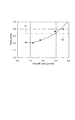
図8は、窒化ガリウム系半導体膜の成長速度と表面粗さ(Rms)との関係を示すグラフである。実験サンプルは、0.7度以下のオフ角を持つ窒化ガリウム基板を用いて作製された。窒化ガリウム膜を形成するときに、III族原料ソース(例えば、TMG)とV族原料ソース(例えば、NH3)とのモル比がほぼ一定になるように、III族原料ソースとV族原料ソースとの供給量を調整している。成長速度が小さくなるにつれて、表面粗さ(Rms)も小さくなる。 FIG. 8 is a graph showing the relationship between the growth rate of the gallium nitride based semiconductor film and the surface roughness (Rms). The experimental sample was produced using a gallium nitride substrate having an off angle of 0.7 degrees or less. When forming the gallium nitride film, the group III source source and the group V source source are set such that the molar ratio between the group III source source (eg, TMG) and the group V source source (eg, NH 3 ) is substantially constant. The supply amount is adjusted. As the growth rate decreases, the surface roughness (Rms) also decreases.
好適な実施例では、窒化ガリウム系半導体膜の成長速度は、毎時1.5マイクロメートル以下であり、図8における領域V1によって示される。表面粗さ(Rms)が0.2ナノメートル程度であり、AFM像には主に原子ステップが現れており、非常に平坦な表面を有する窒化ガリウム系半導体膜が得られている。 In the preferred embodiment, the growth rate of the gallium nitride based semiconductor film is 1.5 micrometers or less per hour, as indicated by region V1 in FIG. The surface roughness (Rms) is 0 . It is about 2 nanometers, and atomic steps mainly appear in the AFM image, and a gallium nitride based semiconductor film having a very flat surface is obtained.
好適な実施例では、原料ガスのV族原料とIII族原料とのモル比[V族原料]/[III族原料]は2000以上3000以下である。窒化ガリウム系半導体膜の成膜速度を小さくするために、ガリウムソースの流量を小さくする。発明者らにより実験によれば、アンモニアソースの流量を小さくすること無しにガリウムソースの流量を小さくすると、表面モフォロジーが乱れる傾向にある。より良好な表面モフォロジーの膜を得るために、上記の原料ガス比に範囲において、ガリウムソースの流量を小さくすると共に、アンモニアソースの流量を小さくする。 In a preferred embodiment, the molar ratio [group V material] / [group III material] of the group V material and group III material of the source gas is 2000 or more and 3000 or less. In order to reduce the deposition rate of the gallium nitride based semiconductor film, the flow rate of the gallium source is reduced. According to experiments by the inventors, when the flow rate of the gallium source is reduced without reducing the flow rate of the ammonia source, the surface morphology tends to be disturbed. In order to obtain a film having a better surface morphology, the flow rate of the gallium source is decreased and the flow rate of the ammonia source is decreased within the above range of the raw material gas ratio.
オフ角および成長速度に関して様々な実験サンプルを作製して、表面モフォロジーの測定を行っている。図9〜図12は、これらの測定結果のうち例示的に示された原子間力顕微鏡の像を示す図面である。 Various experimental samples for off-angle and growth rate are made to measure surface morphology. 9 to 12 are drawings showing atomic force microscope images exemplarily shown in these measurement results.
図9は、オフ角が0.21度の窒化ガリウム基板上に、毎時3.2マイクロメートルの成長速度で成長された窒化ガリウム膜のAFM像を示す。この窒化ガリウム膜では、10マイクロメートル四方の領域内の表面粗さ(Rms)が0.6程度であり、2.5マイクロメートル四方の領域内の表面粗さ(Rms)が0.34程度である。 FIG. 9 shows an AFM image of a gallium nitride film grown at a growth rate of 3.2 micrometers per hour on a gallium nitride substrate having an off angle of 0.21 degrees. In this gallium nitride film, the surface roughness (Rms) in an area of 10 micrometers square is about 0.6, and the surface roughness (Rms) in an area of 2.5 micrometers square is about 0.34. is there.
図10は、オフ角が0.09度の窒化ガリウム基板上に、毎時1.2マイクロメートルの成長速度で成長された窒化ガリウム膜のAFM像を示す。この窒化ガリウム膜では、10マイクロメートル四方の領域内の表面粗さ(Rms)が0.2程度であり、2.5マイクロメートル四方の領域内の表面粗さ(Rms)が0.17程度である。 FIG. 10 shows an AFM image of a gallium nitride film grown at a growth rate of 1.2 micrometers per hour on a gallium nitride substrate having an off angle of 0.09 degrees. In this gallium nitride film, the surface roughness (Rms) in the 10-micrometer square region is about 0.2, and the surface roughness (Rms) in the 2.5-micrometer square region is about 0.17. is there.
図11は、オフ角が1.1度の窒化ガリウム基板上に、毎時3.2マイクロメートルの成長速度で成長された窒化ガリウム膜のAFM像を示す。この窒化ガリウム膜では、10マイクロメートル四方の領域内の表面粗さ(Rms)が0.99程度であり、2.5マイクロメートル四方の領域内の表面粗さ(Rms)が0.67程度である。 FIG. 11 shows an AFM image of a gallium nitride film grown on a gallium nitride substrate with an off angle of 1.1 degrees at a growth rate of 3.2 micrometers per hour. In this gallium nitride film, the surface roughness (Rms) in the 10-micrometer square region is about 0.99, and the surface roughness (Rms) in the 2.5-micrometer square region is about 0.67. is there.
図12は、オフ角が1.5度の窒化ガリウム基板上に、毎時1.2マイクロメートルの成長速度で成長された窒化ガリウム膜のAFM像を示す。この窒化ガリウム膜では、10マイクロメートル四方の領域内の表面粗さ(Rms)が0.5程度であり、2.5マイクロメートル四方の領域内の表面粗さ(Rms)が0.58程度である。 FIG. 12 shows an AFM image of a gallium nitride film grown at a growth rate of 1.2 micrometers per hour on a gallium nitride substrate with an off angle of 1.5 degrees. In this gallium nitride film, the surface roughness (Rms) in the region of 10 micrometers square is about 0.5, and the surface roughness (Rms) in the region of 2.5 micrometers square is about 0.58. is there.
これらの測定結果によれば、成長速度を下げることは表面モフォロジーを良好にするために好適である。図11に示されるように、毎時3.2マイクロメートルの成長速度で成長された窒化ガリウム膜のAFM像には、ステップ状の凹凸が現れている。しかしながら、該ステップ状の凹凸は、より小さい成長速度で作製された窒化ガリウム膜のAFM像には現れていない。このAFM像には、平行にそろった原子ステップが現れており、平坦な表面が得られている。 According to these measurement results, lowering the growth rate is suitable for improving the surface morphology. As shown in FIG. 11, stepped irregularities appear in the AFM image of the gallium nitride film grown at a growth rate of 3.2 micrometers per hour. However, the step-shaped unevenness does not appear in the AFM image of the gallium nitride film manufactured at a lower growth rate. In this AFM image, parallel atomic steps appear, and a flat surface is obtained.
窒化ガリウム基板上に直接に成長されたn型窒化ガリウム膜の表面には、平行な原子ステップが見られ、表面粗さ(Rms)で0.6ナノメートル以下であり、貫通転位密度が1×107cm−2以下であり、(0002)面のX線回折の半値幅200秒以下である。このn型窒化ガリウム膜を用いて発光ダイオードを作製している。この発光ダイオードの発光は均一である。 Parallel atomic steps are observed on the surface of the n-type gallium nitride film directly grown on the gallium nitride substrate, the surface roughness (Rms) is 0.6 nanometers or less, and the threading dislocation density is 1 ×. 10 7 cm −2 or less, and a (0002) plane X-ray diffraction half width of 200 seconds or less. A light emitting diode is manufactured using this n-type gallium nitride film. The light emission of this light emitting diode is uniform.
図13に示される発光ダイオードは、オフ角0.16度の窒化ガリウム基板上に成長速度毎時3.2マイクロメートルで成長された窒化ガリウム膜を有する。図14は、この窒化ガリウム膜の表面の微分干渉顕微鏡像を示す図面である。この微分干渉顕微鏡像は、この窒化ガリウム膜の表面の一部分に六角錘状のパターンが形成されていることを示している。当該部分における発光強度は小さく、それ以外の部分では、この発光ダイオードは概ね均一に発光しており、発光出力は20ミリアンペアで1.2ミリワットである。 The light-emitting diode shown in FIG. 13 has a gallium nitride film grown on a gallium nitride substrate having an off angle of 0.16 degrees at a growth rate of 3.2 micrometers per hour. FIG. 14 is a drawing showing a differential interference microscope image of the surface of the gallium nitride film. This differential interference microscope image shows that a hexagonal pyramid pattern is formed on a part of the surface of the gallium nitride film. The light emission intensity in the portion is small, and in the other portions, the light emitting diode emits light substantially uniformly, and the light emission output is 1.2 milliwatts at 20 milliamperes.
図15は、発光ダイオードの発光像を示す図面である。この発光ダイオードは、オフ角0.4度の窒化ガリウム基板上に成長速度毎時1.2マイクロメートルで成長された窒化ガリウム膜を有する。図16は、この窒化ガリウム膜の表面の微分干渉顕微鏡像を示す図面である。この微分干渉顕微鏡像は、窒化ガリウム膜の表面が平坦であることを示している。この発光ダイオードは全面で均一に発光している。発光出力は、20ミリアンペアで1.9ミリワットである。 FIG. 15 is a view showing a light emission image of the light emitting diode. This light-emitting diode has a gallium nitride film grown on a gallium nitride substrate with an off angle of 0.4 degrees at a growth rate of 1.2 micrometers per hour. FIG. 16 is a drawing showing a differential interference microscope image of the surface of this gallium nitride film. This differential interference microscope image shows that the surface of the gallium nitride film is flat. The light emitting diode emits light uniformly over the entire surface. The light output is 1.9 milliwatts at 20 milliamps.
様々な実験結果を示しながら説明したように、オフ角を調整した窒化ガリウム基板上に、窒化ガリウム膜(窒化ガリウム層)といった窒化ガリウム系半導体膜(窒化ガリウム系半導体層)を成長することによって、以下に示すように良好な表面モフォロジーおよび表面粗さ(Rms)が実現される。 As explained while showing various experimental results, by growing a gallium nitride based semiconductor film (gallium nitride based semiconductor layer) such as a gallium nitride film (gallium nitride layer) on a gallium nitride substrate with an adjusted off angle, Good surface morphology and surface roughness (Rms) are achieved as shown below.
2度未満のオフ角の範囲では、表面モフォロジーは六角錘状のパターン、ステップ状の凹凸、原子ステップあるいはスクラッチ状のパターンを示しており、表面粗さ(Rms)は最大2ナノメートル程度まで小さくなる。この発光ダイオードはほぼ均一に発光する。2ナノメートル未満の表面粗さ(Rms)の表面は、厚さ1〜5ナノメートル程度の井戸層を含む量子井戸構造活性層の下地として好適である。 In the range of an off angle of less than 2 degrees, the surface morphology shows a hexagonal pyramid pattern, stepped irregularities, atomic step or scratch pattern, and the surface roughness (Rms) is small up to about 2 nanometers. Become. This light emitting diode emits light substantially uniformly. A surface having a surface roughness (Rms) of less than 2 nanometers is suitable as a base for a quantum well structure active layer including a well layer having a thickness of about 1 to 5 nanometers.
0.15度より大きく2.0度未満のオフ角の範囲では、表面モフォロジーはステップ状の凹凸、原子ステップあるいはスクラッチ状のパターンを示しており、表面粗さ(Rms)は最大2.0ナノメートル程度である。この発光ダイオードはほぼ均一に発光する。 In the off angle range of greater than 0.15 degrees and less than 2.0 degrees, the surface morphology shows a step-like irregularity, atomic step or scratch-like pattern, and a surface roughness (Rms) of up to 2.0 nanometers. It is about a meter. This light emitting diode emits light substantially uniformly.
0.7度以下のオフ角の範囲では、表面モフォロジーは六角錘状のパターン、ステップ状の凹凸、あるいは原子ステップのパターンを示しており、表面粗さ(Rms)は最大0.5ナノメートル程度まで小さくなる。この発光ダイオードは、ほぼ均一に発光する。 In the off-angle range of 0.7 degrees or less, the surface morphology shows a hexagonal pyramidal pattern, stepped irregularity, or atomic step pattern, and the surface roughness (Rms) is about 0.5 nanometers at the maximum. Becomes smaller. This light emitting diode emits light substantially uniformly.
0.15度より大きく0.7度以下のオフ角の範囲では、表面モフォロジーはステップ状の凹凸あるいは原子ステップを示しており、表面粗さ(Rms)は最大0.5ナノメートル程度まで小さくなる。この発光ダイオードは、均一に発光する。 In the off angle range of greater than 0.15 degrees and less than or equal to 0.7 degrees, the surface morphology shows stepped irregularities or atomic steps, and the surface roughness (Rms) is reduced to a maximum of about 0.5 nanometers. . This light emitting diode emits light uniformly.
0.3度より大きく0.7度以下のオフ角の範囲では、表面モフォロジーは、原子ステップを示す平坦性であり、表面粗さ(Rms)は最大0.3ナノメートル程度まで小さくなる。この発光ダイオードは全面で均一に発光する。例えば、2インチ径の窒化ガリウム基板のオフ角のばらつきが約0.3度であるので、この窒化ガリウム基板のほぼ全面で良好な表面モフォロジーが得られる。 In the off angle range of greater than 0.3 degrees and less than or equal to 0.7 degrees, the surface morphology is flatness indicating atomic steps, and the surface roughness (Rms) decreases to a maximum of about 0.3 nanometers. The light emitting diode emits light uniformly over the entire surface. For example, since the variation in the off angle of a 2-inch gallium nitride substrate is about 0.3 degrees, a good surface morphology can be obtained on almost the entire surface of the gallium nitride substrate.
10マイクロメートル四方の領域における表面粗さ(Rms)が0.6ナノメートル以下である窒化ガリウム膜では、該窒化ガリウム層の貫通転位密度が1×107cm−2以下であり、該窒化ガリウム層は200秒以下の(0002)面のX線回折半値全幅を示す。この発光ダイオードはほぼ均一に発光する。 In a gallium nitride film having a surface roughness (Rms) of 0.6 nanometer or less in a 10-micrometer square region, the threading dislocation density of the gallium nitride layer is 1 × 10 7 cm −2 or less, and the gallium nitride The layer exhibits a full width at half maximum of (0002) plane X-ray diffraction of 200 seconds or less. This light emitting diode emits light substantially uniformly.
好適な実施の形態において本発明の原理を図示し説明してきたが、本発明は、そのような原理から逸脱することなく配置および詳細において変更され得ることは、当業者によって認識される。本実施の形態では、例えば、発光ダイオードといった半導体発光素子を説明したけれども、本発明は、本実施の形態に開示された特定の構成に限定されるものではない。また、本実施の形態では、窒化ガリウム基板上に形成された窒化ガリウム膜について例示的に説明しているけれども、窒化ガリウム系半導体(AlXInYGa1―X−YN、0≦X<1、0≦Y<1、0≦X+Y<1)膜を形成することもできる。したがって、特許請求の範囲およびその精神の範囲から来る全ての修正および変更に権利を請求する。 While the principles of the invention have been illustrated and described in the preferred embodiments, it will be appreciated by those skilled in the art that the invention can be modified in arrangement and detail without departing from such principles. In the present embodiment, for example, a semiconductor light emitting element such as a light emitting diode has been described. However, the present invention is not limited to the specific configuration disclosed in the present embodiment. In this embodiment, a gallium nitride film formed over a gallium nitride substrate is described as an example. However, a gallium nitride-based semiconductor (Al X In Y Ga 1- XYN, 0 ≦ X < 1, 0 ≦ Y <1, 0 ≦ X + Y <1) A film can also be formed. We therefore claim all modifications and changes that come within the scope and spirit of the following claims.
1…窒化ガリウム基板、3…OMVPE成膜装置、9…窒化ガリウム系膜、12…半導体基板生産物、11…窒化ガリウム系膜、13…窒化ガリウム系膜、15…窒化ガリウム系膜、17…半導体基板生産物、19…オーミック電極、21…オーミック電極、23…パッド電極膜、32…発光ダイオード、33…窒化ガリウム支持基体、35…窒化ガリウム系半導体層、37…活性層、39a〜39e…井戸層、41a〜41d…障壁層、43…AlGaN層、45…コンタクト層、47…オーミック層、49…オーミック層、51…パッド電極
DESCRIPTION OF
Claims (19)
窒化ガリウム基板を準備する工程を備え、前記窒化ガリウム基板の主面の全体において該主面の法線と前記窒化ガリウム基板のC軸とは2度未満の角度をなしており、前記主面の法線と前記窒化ガリウム基板のC軸とは0度より大きな角度をなし、
窒化ガリウム系半導体膜を形成する前に、アンモニアおよび水素を含むプロセスガスを供給して、摂氏1100度以上の温度で前記窒化ガリウム基板の熱処理を有機金属気相成長装置を用いて10分以上の時間で行う工程を備え、
V族原料およびIII族原料を供給して前記窒化ガリウム基板の前記主面上に、10マイクロメートル四方の領域において0.6ナノメートル以下の最小自乗平方根表面粗さを有する窒化ガリウム系半導体膜を前記有機金属気相成長装置を用いて形成する工程を備え、前記窒化ガリウム系半導体膜は90キロパスカル以下の圧力で形成され、前記窒化ガリウム系半導体膜の成長速度は毎時1.5マイクロメートル以下であり、前記原料ガスのV族原料とIII族原料とのモル比[V族原料]/[III族原料]は2000以上3000以下である、ことを特徴とする方法。 A method of forming a gallium nitride based semiconductor film,
A step of preparing a gallium nitride substrate, wherein the normal of the main surface and the C axis of the gallium nitride substrate form an angle of less than 2 degrees over the entire main surface of the gallium nitride substrate , The normal and the C axis of the gallium nitride substrate form an angle greater than 0 degrees,
Before forming the gallium nitride based semiconductor film, a process gas containing ammonia and hydrogen is supplied, and the gallium nitride substrate is heat-treated at a temperature of 1100 degrees Celsius or higher for 10 minutes or more using a metal organic vapor phase growth apparatus. With a time-consuming process,
A gallium nitride based semiconductor film having a least square square surface roughness of 0.6 nanometers or less in a 10 micrometer square region on the main surface of the gallium nitride substrate by supplying a group V material and a group III material. e Bei forming using the metal organic vapor phase growth apparatus, the gallium nitride based semiconductor film is formed with a pressure 90 kg pascals, the growth rate of the gallium nitride-based semiconductor film per hour 1.5 micrometers The method is characterized in that the molar ratio [Group V material] / [Group III material] of the Group V material and Group III material of the source gas is 2000 or more and 3000 or less .
前記活性層はSQW構造またはMQW構造を有する、ことを特徴とする請求項1〜8のいずれか一項に記載された方法。The method according to claim 1, wherein the active layer has an SQW structure or an MQW structure.
主面を有する窒化ガリウム基板と、
前記窒化ガリウム基板の主面上に設けられた少なくとも一層の窒化ガリウム系半導体膜と
を備え、
前記窒化ガリウム基板の主面の全体において該主面の法線と前記窒化ガリウム基板のC軸とは2度未満の角度をなしており、
前記主面の法線と前記窒化ガリウム基板のC軸とは0度より大きい角度をなし、
前記窒化ガリウム系半導体膜の最小自乗平方根表面粗さは、10マイクロメートル四方の領域において0.6ナノメートル以下である、ことを特徴とする半導体基板生産物。 A semiconductor substrate product produced by the method according to any one of claims 1 to 4,
A gallium nitride substrate having a main surface;
At least one gallium nitride based semiconductor film provided on the main surface of the gallium nitride substrate;
With
The normal line of the main surface and the C axis of the gallium nitride substrate form an angle of less than 2 degrees over the entire main surface of the gallium nitride substrate.
The normal of the main surface and the C axis of the gallium nitride substrate form an angle greater than 0 degrees,
The minimum root-surface roughness of the GaN-based semiconductor film, 10 in micrometers square area is 0.6 nm or less, the semiconductor substrate product, characterized in that.
Priority Applications (1)
| Application Number | Priority Date | Filing Date | Title |
|---|---|---|---|
| JP2003396183A JP3894191B2 (en) | 2003-11-26 | 2003-11-26 | Method for forming gallium nitride based semiconductor film and semiconductor substrate product |
Applications Claiming Priority (1)
| Application Number | Priority Date | Filing Date | Title |
|---|---|---|---|
| JP2003396183A JP3894191B2 (en) | 2003-11-26 | 2003-11-26 | Method for forming gallium nitride based semiconductor film and semiconductor substrate product |
Publications (2)
| Publication Number | Publication Date |
|---|---|
| JP2005159047A JP2005159047A (en) | 2005-06-16 |
| JP3894191B2 true JP3894191B2 (en) | 2007-03-14 |
Family
ID=34721750
Family Applications (1)
| Application Number | Title | Priority Date | Filing Date |
|---|---|---|---|
| JP2003396183A Expired - Fee Related JP3894191B2 (en) | 2003-11-26 | 2003-11-26 | Method for forming gallium nitride based semiconductor film and semiconductor substrate product |
Country Status (1)
| Country | Link |
|---|---|
| JP (1) | JP3894191B2 (en) |
Cited By (1)
| Publication number | Priority date | Publication date | Assignee | Title |
|---|---|---|---|---|
| WO2014156914A1 (en) | 2013-03-29 | 2014-10-02 | 日本碍子株式会社 | Method for processing group-iii nitride substrate and method for manufacturing epitaxial substrate |
Families Citing this family (12)
| Publication number | Priority date | Publication date | Assignee | Title |
|---|---|---|---|---|
| DE102005035722B9 (en) * | 2005-07-29 | 2021-11-18 | OSRAM Opto Semiconductors Gesellschaft mit beschränkter Haftung | Optoelectronic semiconductor chip and method for its production |
| US7755103B2 (en) | 2006-08-03 | 2010-07-13 | Sumitomo Electric Industries, Ltd. | Nitride gallium semiconductor substrate and nitride semiconductor epitaxial substrate |
| JP4232837B2 (en) | 2007-03-28 | 2009-03-04 | 住友電気工業株式会社 | Method for fabricating nitride semiconductor light emitting device |
| US9048100B2 (en) * | 2007-11-21 | 2015-06-02 | Mitsubishi Chemical Corporation | Nitride semiconductor and nitride semiconductor crystal growth method |
| JP2009238772A (en) * | 2008-03-25 | 2009-10-15 | Sumitomo Electric Ind Ltd | Epitaxial substrate, and manufacturing method of epitaxial substrate |
| JP2009253047A (en) * | 2008-04-07 | 2009-10-29 | Sumitomo Electric Ind Ltd | Group iii nitride light emitting element, and epitaxial wafer |
| JP4835662B2 (en) * | 2008-08-27 | 2011-12-14 | 住友電気工業株式会社 | Method for fabricating nitride-based semiconductor light-emitting device and method for fabricating epitaxial wafer |
| JP4692602B2 (en) | 2008-09-26 | 2011-06-01 | 住友電気工業株式会社 | Gallium nitride based epitaxial wafer and method for producing epitaxial wafer |
| JP5743928B2 (en) * | 2012-03-05 | 2015-07-01 | 日立金属株式会社 | Gallium nitride semiconductor epitaxial wafer and method for manufacturing the same |
| JP5641029B2 (en) * | 2012-09-24 | 2014-12-17 | 住友電気工業株式会社 | Group III nitride electronic devices |
| CN104641453B (en) | 2012-10-12 | 2018-03-30 | 住友电气工业株式会社 | Group III nitride composite substrate and its manufacture method and the method for manufacturing Group III nitride semiconductor device |
| EP3159983B1 (en) * | 2014-06-17 | 2023-08-02 | Sony Group Corporation | Light emitting element and method for manufacturing same |
Family Cites Families (2)
| Publication number | Priority date | Publication date | Assignee | Title |
|---|---|---|---|---|
| US6447604B1 (en) * | 2000-03-13 | 2002-09-10 | Advanced Technology Materials, Inc. | Method for achieving improved epitaxy quality (surface texture and defect density) on free-standing (aluminum, indium, gallium) nitride ((al,in,ga)n) substrates for opto-electronic and electronic devices |
| JP4567896B2 (en) * | 2001-02-09 | 2010-10-20 | シャープ株式会社 | Manufacturing method of semiconductor light emitting device |
-
2003
- 2003-11-26 JP JP2003396183A patent/JP3894191B2/en not_active Expired - Fee Related
Cited By (3)
| Publication number | Priority date | Publication date | Assignee | Title |
|---|---|---|---|---|
| WO2014156914A1 (en) | 2013-03-29 | 2014-10-02 | 日本碍子株式会社 | Method for processing group-iii nitride substrate and method for manufacturing epitaxial substrate |
| US9196480B2 (en) | 2013-03-29 | 2015-11-24 | Ngk Insulators, Ltd. | Method for treating group III nitride substrate and method for manufacturing epitaxial substrate |
| KR20150140202A (en) | 2013-03-29 | 2015-12-15 | 엔지케이 인슐레이터 엘티디 | Method for treating group iii nitride substrate and method for manufacturing epitaxial substrate |
Also Published As
| Publication number | Publication date |
|---|---|
| JP2005159047A (en) | 2005-06-16 |
Similar Documents
| Publication | Publication Date | Title |
|---|---|---|
| US6693021B1 (en) | GaN single crystal substrate and method of making the same | |
| US6455877B1 (en) | III-N compound semiconductor device | |
| JP3036495B2 (en) | Method for manufacturing gallium nitride-based compound semiconductor | |
| US7847313B2 (en) | Group III-V nitride-based semiconductor substrate and group III-V nitride-based light emitting device | |
| US7951617B2 (en) | Group III nitride semiconductor stacked structure and production method thereof | |
| JP5099763B2 (en) | Substrate manufacturing method and group III nitride semiconductor crystal | |
| KR20110088483A (en) | Method of manufacturing single-crystal gan substrate, and single-crystal gan substrate | |
| US20030157738A1 (en) | Method for manufacturing gallium nitride compound semiconductor | |
| JP3894191B2 (en) | Method for forming gallium nitride based semiconductor film and semiconductor substrate product | |
| US20150249122A1 (en) | Aluminum Nitride Substrate and Group-III Nitride Laminate | |
| JP4337560B2 (en) | Method for manufacturing single crystal gallium nitride substrate, gallium nitride substrate, and nitride semiconductor epitaxial substrate | |
| JPH06196757A (en) | Method of growing indium gallium nitride semiconductor | |
| JPH11251632A (en) | Manufacture of gallium nitride semiconductor element | |
| US20110163323A1 (en) | GaN SINGLE CRYSTAL SUBSTRATE AND METHOD OF MAKING THE SAME | |
| JP2006147849A (en) | Group iii-v nitride semiconductor substrate and its evaluation method | |
| JP4232837B2 (en) | Method for fabricating nitride semiconductor light emitting device | |
| US8236103B2 (en) | Group III nitride semiconductor crystal, production method thereof and group III nitride semiconductor epitaxial wafer | |
| JP2000252217A (en) | Production of compound semiconductor | |
| JP3991823B2 (en) | Group III nitride semiconductor crystal, method for producing the same, group III nitride semiconductor epitaxial wafer | |
| JP5015480B2 (en) | Manufacturing method of semiconductor single crystal substrate | |
| JPH06209122A (en) | Indium gallium nitride semiconductor and growing method thereof | |
| JP3274907B2 (en) | Method for growing indium gallium nitride compound semiconductor | |
| JP5093127B2 (en) | Gallium nitride substrate and nitride semiconductor epitaxial substrate | |
| JP2677221B2 (en) | Method for growing nitride-based III-V compound semiconductor crystal | |
| JP3203282B2 (en) | Indium gallium nitride semiconductor for light emitting devices |
Legal Events
| Date | Code | Title | Description |
|---|---|---|---|
| A977 | Report on retrieval |
Free format text: JAPANESE INTERMEDIATE CODE: A971007 Effective date: 20051207 |
|
| A131 | Notification of reasons for refusal |
Free format text: JAPANESE INTERMEDIATE CODE: A131 Effective date: 20051213 |
|
| A521 | Written amendment |
Free format text: JAPANESE INTERMEDIATE CODE: A523 Effective date: 20060210 |
|
| TRDD | Decision of grant or rejection written | ||
| A01 | Written decision to grant a patent or to grant a registration (utility model) |
Free format text: JAPANESE INTERMEDIATE CODE: A01 Effective date: 20061121 |
|
| A61 | First payment of annual fees (during grant procedure) |
Free format text: JAPANESE INTERMEDIATE CODE: A61 Effective date: 20061204 |
|
| R150 | Certificate of patent or registration of utility model |
Free format text: JAPANESE INTERMEDIATE CODE: R150 Ref document number: 3894191 Country of ref document: JP Free format text: JAPANESE INTERMEDIATE CODE: R150 |
|
| FPAY | Renewal fee payment (event date is renewal date of database) |
Free format text: PAYMENT UNTIL: 20101222 Year of fee payment: 4 |
|
| FPAY | Renewal fee payment (event date is renewal date of database) |
Free format text: PAYMENT UNTIL: 20101222 Year of fee payment: 4 |
|
| FPAY | Renewal fee payment (event date is renewal date of database) |
Free format text: PAYMENT UNTIL: 20111222 Year of fee payment: 5 |
|
| FPAY | Renewal fee payment (event date is renewal date of database) |
Free format text: PAYMENT UNTIL: 20111222 Year of fee payment: 5 |
|
| FPAY | Renewal fee payment (event date is renewal date of database) |
Free format text: PAYMENT UNTIL: 20121222 Year of fee payment: 6 |
|
| FPAY | Renewal fee payment (event date is renewal date of database) |
Free format text: PAYMENT UNTIL: 20121222 Year of fee payment: 6 |
|
| FPAY | Renewal fee payment (event date is renewal date of database) |
Free format text: PAYMENT UNTIL: 20131222 Year of fee payment: 7 |
|
| R250 | Receipt of annual fees |
Free format text: JAPANESE INTERMEDIATE CODE: R250 |
|
| R250 | Receipt of annual fees |
Free format text: JAPANESE INTERMEDIATE CODE: R250 |
|
| R250 | Receipt of annual fees |
Free format text: JAPANESE INTERMEDIATE CODE: R250 |
|
| R250 | Receipt of annual fees |
Free format text: JAPANESE INTERMEDIATE CODE: R250 |
|
| LAPS | Cancellation because of no payment of annual fees |