EP3159983B1 - Light emitting element and method for manufacturing same - Google Patents
Light emitting element and method for manufacturing same Download PDFInfo
- Publication number
- EP3159983B1 EP3159983B1 EP15809837.6A EP15809837A EP3159983B1 EP 3159983 B1 EP3159983 B1 EP 3159983B1 EP 15809837 A EP15809837 A EP 15809837A EP 3159983 B1 EP3159983 B1 EP 3159983B1
- Authority
- EP
- European Patent Office
- Prior art keywords
- layer
- light
- compound semiconductor
- light reflecting
- emitting element
- Prior art date
- Legal status (The legal status is an assumption and is not a legal conclusion. Google has not performed a legal analysis and makes no representation as to the accuracy of the status listed.)
- Active
Links
- 238000004519 manufacturing process Methods 0.000 title claims description 32
- 238000000034 method Methods 0.000 title description 74
- 239000004065 semiconductor Substances 0.000 claims description 173
- 150000001875 compounds Chemical class 0.000 claims description 153
- JMASRVWKEDWRBT-UHFFFAOYSA-N Gallium nitride Chemical compound [Ga]#N JMASRVWKEDWRBT-UHFFFAOYSA-N 0.000 claims description 101
- 239000000463 material Substances 0.000 claims description 17
- 230000003746 surface roughness Effects 0.000 claims description 13
- TWNQGVIAIRXVLR-UHFFFAOYSA-N oxo(oxoalumanyloxy)alumane Chemical compound O=[Al]O[Al]=O TWNQGVIAIRXVLR-UHFFFAOYSA-N 0.000 claims description 9
- 229910052581 Si3N4 Inorganic materials 0.000 claims description 8
- HQVNEWCFYHHQES-UHFFFAOYSA-N silicon nitride Chemical compound N12[Si]34N5[Si]62N3[Si]51N64 HQVNEWCFYHHQES-UHFFFAOYSA-N 0.000 claims description 8
- GWEVSGVZZGPLCZ-UHFFFAOYSA-N Titan oxide Chemical compound O=[Ti]=O GWEVSGVZZGPLCZ-UHFFFAOYSA-N 0.000 claims description 7
- 229910000484 niobium oxide Inorganic materials 0.000 claims description 7
- BPUBBGLMJRNUCC-UHFFFAOYSA-N oxygen(2-);tantalum(5+) Chemical compound [O-2].[O-2].[O-2].[O-2].[O-2].[Ta+5].[Ta+5] BPUBBGLMJRNUCC-UHFFFAOYSA-N 0.000 claims description 7
- RVTZCBVAJQQJTK-UHFFFAOYSA-N oxygen(2-);zirconium(4+) Chemical compound [O-2].[O-2].[Zr+4] RVTZCBVAJQQJTK-UHFFFAOYSA-N 0.000 claims description 7
- 229910001936 tantalum oxide Inorganic materials 0.000 claims description 7
- OGIDPMRJRNCKJF-UHFFFAOYSA-N titanium oxide Inorganic materials [Ti]=O OGIDPMRJRNCKJF-UHFFFAOYSA-N 0.000 claims description 7
- 229910001928 zirconium oxide Inorganic materials 0.000 claims description 7
- 239000000395 magnesium oxide Substances 0.000 claims description 5
- CPLXHLVBOLITMK-UHFFFAOYSA-N magnesium oxide Inorganic materials [Mg]=O CPLXHLVBOLITMK-UHFFFAOYSA-N 0.000 claims description 5
- AXZKOIWUVFPNLO-UHFFFAOYSA-N magnesium;oxygen(2-) Chemical compound [O-2].[Mg+2] AXZKOIWUVFPNLO-UHFFFAOYSA-N 0.000 claims description 5
- URLJKFSTXLNXLG-UHFFFAOYSA-N niobium(5+);oxygen(2-) Chemical compound [O-2].[O-2].[O-2].[O-2].[O-2].[Nb+5].[Nb+5] URLJKFSTXLNXLG-UHFFFAOYSA-N 0.000 claims description 4
- PMHQVHHXPFUNSP-UHFFFAOYSA-M copper(1+);methylsulfanylmethane;bromide Chemical compound Br[Cu].CSC PMHQVHHXPFUNSP-UHFFFAOYSA-M 0.000 claims description 3
- 239000010410 layer Substances 0.000 description 508
- 239000000758 substrate Substances 0.000 description 48
- 239000010931 gold Substances 0.000 description 26
- 239000010936 titanium Substances 0.000 description 20
- PXHVJJICTQNCMI-UHFFFAOYSA-N Nickel Chemical compound [Ni] PXHVJJICTQNCMI-UHFFFAOYSA-N 0.000 description 18
- KDLHZDBZIXYQEI-UHFFFAOYSA-N palladium Substances [Pd] KDLHZDBZIXYQEI-UHFFFAOYSA-N 0.000 description 17
- 150000004767 nitrides Chemical class 0.000 description 16
- BASFCYQUMIYNBI-UHFFFAOYSA-N platinum Chemical compound [Pt] BASFCYQUMIYNBI-UHFFFAOYSA-N 0.000 description 16
- 239000013078 crystal Substances 0.000 description 14
- 229910052814 silicon oxide Inorganic materials 0.000 description 14
- 239000007789 gas Substances 0.000 description 13
- 229910004205 SiNX Inorganic materials 0.000 description 12
- 238000012986 modification Methods 0.000 description 11
- 230000004048 modification Effects 0.000 description 11
- XLOMVQKBTHCTTD-UHFFFAOYSA-N Zinc monoxide Chemical compound [Zn]=O XLOMVQKBTHCTTD-UHFFFAOYSA-N 0.000 description 10
- 238000005304 joining Methods 0.000 description 10
- 125000004429 atom Chemical group 0.000 description 9
- 229910052737 gold Inorganic materials 0.000 description 9
- IJGRMHOSHXDMSA-UHFFFAOYSA-N Atomic nitrogen Chemical compound N#N IJGRMHOSHXDMSA-UHFFFAOYSA-N 0.000 description 8
- 239000011777 magnesium Substances 0.000 description 8
- 229910052751 metal Inorganic materials 0.000 description 8
- 239000002184 metal Substances 0.000 description 8
- 230000004888 barrier function Effects 0.000 description 7
- 239000003989 dielectric material Substances 0.000 description 7
- 230000003287 optical effect Effects 0.000 description 7
- 230000010355 oscillation Effects 0.000 description 7
- XOLBLPGZBRYERU-UHFFFAOYSA-N tin dioxide Chemical compound O=[Sn]=O XOLBLPGZBRYERU-UHFFFAOYSA-N 0.000 description 7
- 229910052719 titanium Inorganic materials 0.000 description 7
- 229910052759 nickel Inorganic materials 0.000 description 6
- 238000005240 physical vapour deposition Methods 0.000 description 6
- 229910052697 platinum Inorganic materials 0.000 description 6
- 238000004544 sputter deposition Methods 0.000 description 6
- XCZXGTMEAKBVPV-UHFFFAOYSA-N trimethylgallium Chemical compound C[Ga](C)C XCZXGTMEAKBVPV-UHFFFAOYSA-N 0.000 description 6
- 239000011787 zinc oxide Substances 0.000 description 6
- 230000002411 adverse Effects 0.000 description 5
- 229910052782 aluminium Inorganic materials 0.000 description 5
- 238000005229 chemical vapour deposition Methods 0.000 description 5
- 239000004020 conductor Substances 0.000 description 5
- 230000000694 effects Effects 0.000 description 5
- 239000012535 impurity Substances 0.000 description 5
- 238000002488 metal-organic chemical vapour deposition Methods 0.000 description 5
- 229910052763 palladium Inorganic materials 0.000 description 5
- 229910052594 sapphire Inorganic materials 0.000 description 5
- 239000010980 sapphire Substances 0.000 description 5
- 229910052710 silicon Inorganic materials 0.000 description 5
- 239000000243 solution Substances 0.000 description 5
- 229910002704 AlGaN Inorganic materials 0.000 description 4
- MHAJPDPJQMAIIY-UHFFFAOYSA-N Hydrogen peroxide Chemical compound OO MHAJPDPJQMAIIY-UHFFFAOYSA-N 0.000 description 4
- 229910045601 alloy Inorganic materials 0.000 description 4
- 239000000956 alloy Substances 0.000 description 4
- 230000015572 biosynthetic process Effects 0.000 description 4
- 239000011651 chromium Substances 0.000 description 4
- 230000007547 defect Effects 0.000 description 4
- 239000002019 doping agent Substances 0.000 description 4
- PCHJSUWPFVWCPO-UHFFFAOYSA-N gold Chemical compound [Au] PCHJSUWPFVWCPO-UHFFFAOYSA-N 0.000 description 4
- 229910052757 nitrogen Inorganic materials 0.000 description 4
- 125000004433 nitrogen atom Chemical group N* 0.000 description 4
- 238000005498 polishing Methods 0.000 description 4
- VYPSYNLAJGMNEJ-UHFFFAOYSA-N silicon dioxide Inorganic materials O=[Si]=O VYPSYNLAJGMNEJ-UHFFFAOYSA-N 0.000 description 4
- 229910000679 solder Inorganic materials 0.000 description 4
- 239000000126 substance Substances 0.000 description 4
- 238000007740 vapor deposition Methods 0.000 description 4
- 208000012868 Overgrowth Diseases 0.000 description 3
- BLRPTPMANUNPDV-UHFFFAOYSA-N Silane Chemical compound [SiH4] BLRPTPMANUNPDV-UHFFFAOYSA-N 0.000 description 3
- XUIMIQQOPSSXEZ-UHFFFAOYSA-N Silicon Chemical compound [Si] XUIMIQQOPSSXEZ-UHFFFAOYSA-N 0.000 description 3
- HEMHJVSKTPXQMS-UHFFFAOYSA-M Sodium hydroxide Chemical compound [OH-].[Na+] HEMHJVSKTPXQMS-UHFFFAOYSA-M 0.000 description 3
- XAGFODPZIPBFFR-UHFFFAOYSA-N aluminium Chemical compound [Al] XAGFODPZIPBFFR-UHFFFAOYSA-N 0.000 description 3
- 229910052681 coesite Inorganic materials 0.000 description 3
- 229910052906 cristobalite Inorganic materials 0.000 description 3
- 239000010703 silicon Substances 0.000 description 3
- 239000000377 silicon dioxide Substances 0.000 description 3
- 229910052682 stishovite Inorganic materials 0.000 description 3
- 239000002344 surface layer Substances 0.000 description 3
- 229910052718 tin Inorganic materials 0.000 description 3
- 229910052905 tridymite Inorganic materials 0.000 description 3
- JLTRXTDYQLMHGR-UHFFFAOYSA-N trimethylaluminium Chemical compound C[Al](C)C JLTRXTDYQLMHGR-UHFFFAOYSA-N 0.000 description 3
- IBEFSUTVZWZJEL-UHFFFAOYSA-N trimethylindium Chemical compound C[In](C)C IBEFSUTVZWZJEL-UHFFFAOYSA-N 0.000 description 3
- QGZKDVFQNNGYKY-UHFFFAOYSA-N Ammonia Chemical compound N QGZKDVFQNNGYKY-UHFFFAOYSA-N 0.000 description 2
- OAKJQQAXSVQMHS-UHFFFAOYSA-N Hydrazine Chemical compound NN OAKJQQAXSVQMHS-UHFFFAOYSA-N 0.000 description 2
- VEXZGXHMUGYJMC-UHFFFAOYSA-N Hydrochloric acid Chemical compound Cl VEXZGXHMUGYJMC-UHFFFAOYSA-N 0.000 description 2
- NBIIXXVUZAFLBC-UHFFFAOYSA-N Phosphoric acid Chemical compound OP(O)(O)=O NBIIXXVUZAFLBC-UHFFFAOYSA-N 0.000 description 2
- ATJFFYVFTNAWJD-UHFFFAOYSA-N Tin Chemical compound [Sn] ATJFFYVFTNAWJD-UHFFFAOYSA-N 0.000 description 2
- RTAQQCXQSZGOHL-UHFFFAOYSA-N Titanium Chemical compound [Ti] RTAQQCXQSZGOHL-UHFFFAOYSA-N 0.000 description 2
- USZGMDQWECZTIQ-UHFFFAOYSA-N [Mg](C1C=CC=C1)C1C=CC=C1 Chemical compound [Mg](C1C=CC=C1)C1C=CC=C1 USZGMDQWECZTIQ-UHFFFAOYSA-N 0.000 description 2
- 239000002585 base Substances 0.000 description 2
- 229910052796 boron Inorganic materials 0.000 description 2
- 229910052799 carbon Inorganic materials 0.000 description 2
- 238000005253 cladding Methods 0.000 description 2
- 239000010949 copper Substances 0.000 description 2
- 238000000151 deposition Methods 0.000 description 2
- 230000008021 deposition Effects 0.000 description 2
- 238000005530 etching Methods 0.000 description 2
- 229910052733 gallium Inorganic materials 0.000 description 2
- 229910052738 indium Inorganic materials 0.000 description 2
- APFVFJFRJDLVQX-UHFFFAOYSA-N indium atom Chemical compound [In] APFVFJFRJDLVQX-UHFFFAOYSA-N 0.000 description 2
- PJXISJQVUVHSOJ-UHFFFAOYSA-N indium(III) oxide Inorganic materials [O-2].[O-2].[O-2].[In+3].[In+3] PJXISJQVUVHSOJ-UHFFFAOYSA-N 0.000 description 2
- 239000011810 insulating material Substances 0.000 description 2
- 238000002955 isolation Methods 0.000 description 2
- 229910052749 magnesium Inorganic materials 0.000 description 2
- 238000001451 molecular beam epitaxy Methods 0.000 description 2
- 238000004806 packaging method and process Methods 0.000 description 2
- 239000010948 rhodium Substances 0.000 description 2
- 238000007789 sealing Methods 0.000 description 2
- 229910052709 silver Inorganic materials 0.000 description 2
- 239000002356 single layer Substances 0.000 description 2
- RGGPNXQUMRMPRA-UHFFFAOYSA-N triethylgallium Chemical compound CC[Ga](CC)CC RGGPNXQUMRMPRA-UHFFFAOYSA-N 0.000 description 2
- 229910052725 zinc Inorganic materials 0.000 description 2
- 239000011701 zinc Substances 0.000 description 2
- -1 AlNX Inorganic materials 0.000 description 1
- NLXLAEXVIDQMFP-UHFFFAOYSA-N Ammonium chloride Substances [NH4+].[Cl-] NLXLAEXVIDQMFP-UHFFFAOYSA-N 0.000 description 1
- VHUUQVKOLVNVRT-UHFFFAOYSA-N Ammonium hydroxide Chemical compound [NH4+].[OH-] VHUUQVKOLVNVRT-UHFFFAOYSA-N 0.000 description 1
- ZOXJGFHDIHLPTG-UHFFFAOYSA-N Boron Chemical compound [B] ZOXJGFHDIHLPTG-UHFFFAOYSA-N 0.000 description 1
- NTWRPUHOZUFEDH-UHFFFAOYSA-N C[Mg]C1C=CC=C1 Chemical compound C[Mg]C1C=CC=C1 NTWRPUHOZUFEDH-UHFFFAOYSA-N 0.000 description 1
- VYZAMTAEIAYCRO-UHFFFAOYSA-N Chromium Chemical compound [Cr] VYZAMTAEIAYCRO-UHFFFAOYSA-N 0.000 description 1
- RYGMFSIKBFXOCR-UHFFFAOYSA-N Copper Chemical compound [Cu] RYGMFSIKBFXOCR-UHFFFAOYSA-N 0.000 description 1
- MYMOFIZGZYHOMD-UHFFFAOYSA-N Dioxygen Chemical compound O=O MYMOFIZGZYHOMD-UHFFFAOYSA-N 0.000 description 1
- KRHYYFGTRYWZRS-UHFFFAOYSA-M Fluoride anion Chemical compound [F-] KRHYYFGTRYWZRS-UHFFFAOYSA-M 0.000 description 1
- GYHNNYVSQQEPJS-UHFFFAOYSA-N Gallium Chemical compound [Ga] GYHNNYVSQQEPJS-UHFFFAOYSA-N 0.000 description 1
- 229910001218 Gallium arsenide Inorganic materials 0.000 description 1
- 229910010936 LiGaO2 Inorganic materials 0.000 description 1
- FYYHWMGAXLPEAU-UHFFFAOYSA-N Magnesium Chemical compound [Mg] FYYHWMGAXLPEAU-UHFFFAOYSA-N 0.000 description 1
- 229910026161 MgAl2O4 Inorganic materials 0.000 description 1
- CBENFWSGALASAD-UHFFFAOYSA-N Ozone Chemical compound [O-][O+]=O CBENFWSGALASAD-UHFFFAOYSA-N 0.000 description 1
- OAICVXFJPJFONN-UHFFFAOYSA-N Phosphorus Chemical compound [P] OAICVXFJPJFONN-UHFFFAOYSA-N 0.000 description 1
- KWYUFKZDYYNOTN-UHFFFAOYSA-M Potassium hydroxide Chemical compound [OH-].[K+] KWYUFKZDYYNOTN-UHFFFAOYSA-M 0.000 description 1
- BQCADISMDOOEFD-UHFFFAOYSA-N Silver Chemical compound [Ag] BQCADISMDOOEFD-UHFFFAOYSA-N 0.000 description 1
- QAOWNCQODCNURD-UHFFFAOYSA-N Sulfuric acid Chemical compound OS(O)(=O)=O QAOWNCQODCNURD-UHFFFAOYSA-N 0.000 description 1
- 230000002730 additional effect Effects 0.000 description 1
- 239000002390 adhesive tape Substances 0.000 description 1
- 239000003513 alkali Substances 0.000 description 1
- PNEYBMLMFCGWSK-UHFFFAOYSA-N aluminium oxide Inorganic materials [O-2].[O-2].[O-2].[Al+3].[Al+3] PNEYBMLMFCGWSK-UHFFFAOYSA-N 0.000 description 1
- 229910000147 aluminium phosphate Inorganic materials 0.000 description 1
- 235000011114 ammonium hydroxide Nutrition 0.000 description 1
- 229910052787 antimony Inorganic materials 0.000 description 1
- WATWJIUSRGPENY-UHFFFAOYSA-N antimony atom Chemical compound [Sb] WATWJIUSRGPENY-UHFFFAOYSA-N 0.000 description 1
- 239000007864 aqueous solution Substances 0.000 description 1
- 238000000149 argon plasma sintering Methods 0.000 description 1
- 229910052785 arsenic Inorganic materials 0.000 description 1
- RQNWIZPPADIBDY-UHFFFAOYSA-N arsenic atom Chemical compound [As] RQNWIZPPADIBDY-UHFFFAOYSA-N 0.000 description 1
- 229910052788 barium Inorganic materials 0.000 description 1
- 229910052790 beryllium Inorganic materials 0.000 description 1
- 229910052793 cadmium Inorganic materials 0.000 description 1
- 229910052791 calcium Inorganic materials 0.000 description 1
- 238000006243 chemical reaction Methods 0.000 description 1
- 229910052804 chromium Inorganic materials 0.000 description 1
- 229910017052 cobalt Inorganic materials 0.000 description 1
- 239000010941 cobalt Substances 0.000 description 1
- GUTLYIVDDKVIGB-UHFFFAOYSA-N cobalt atom Chemical compound [Co] GUTLYIVDDKVIGB-UHFFFAOYSA-N 0.000 description 1
- 229910052802 copper Inorganic materials 0.000 description 1
- 230000006866 deterioration Effects 0.000 description 1
- AJNVQOSZGJRYEI-UHFFFAOYSA-N digallium;oxygen(2-) Chemical compound [O-2].[O-2].[O-2].[Ga+3].[Ga+3] AJNVQOSZGJRYEI-UHFFFAOYSA-N 0.000 description 1
- 229910001882 dioxygen Inorganic materials 0.000 description 1
- 238000001312 dry etching Methods 0.000 description 1
- 230000005489 elastic deformation Effects 0.000 description 1
- 229910001195 gallium oxide Inorganic materials 0.000 description 1
- 229910052732 germanium Inorganic materials 0.000 description 1
- 229910052735 hafnium Inorganic materials 0.000 description 1
- 229910052736 halogen Inorganic materials 0.000 description 1
- 150000002367 halogens Chemical class 0.000 description 1
- 230000017525 heat dissipation Effects 0.000 description 1
- 150000004678 hydrides Chemical class 0.000 description 1
- AMGQUBHHOARCQH-UHFFFAOYSA-N indium;oxotin Chemical compound [In].[Sn]=O AMGQUBHHOARCQH-UHFFFAOYSA-N 0.000 description 1
- 239000011261 inert gas Substances 0.000 description 1
- 238000007735 ion beam assisted deposition Methods 0.000 description 1
- 238000007733 ion plating Methods 0.000 description 1
- 238000000608 laser ablation Methods 0.000 description 1
- 238000001459 lithography Methods 0.000 description 1
- 229910052753 mercury Inorganic materials 0.000 description 1
- 239000000203 mixture Substances 0.000 description 1
- 229910000480 nickel oxide Inorganic materials 0.000 description 1
- 229910052758 niobium Inorganic materials 0.000 description 1
- 239000010955 niobium Substances 0.000 description 1
- 238000005121 nitriding Methods 0.000 description 1
- 239000011368 organic material Substances 0.000 description 1
- 230000003647 oxidation Effects 0.000 description 1
- 238000007254 oxidation reaction Methods 0.000 description 1
- 230000001590 oxidative effect Effects 0.000 description 1
- GNRSAWUEBMWBQH-UHFFFAOYSA-N oxonickel Chemical compound [Ni]=O GNRSAWUEBMWBQH-UHFFFAOYSA-N 0.000 description 1
- 229910052760 oxygen Inorganic materials 0.000 description 1
- 229910052698 phosphorus Inorganic materials 0.000 description 1
- 239000011574 phosphorus Substances 0.000 description 1
- 239000004033 plastic Substances 0.000 description 1
- 229920001721 polyimide Polymers 0.000 description 1
- 239000009719 polyimide resin Substances 0.000 description 1
- 238000007781 pre-processing Methods 0.000 description 1
- 238000005546 reactive sputtering Methods 0.000 description 1
- 229910052703 rhodium Inorganic materials 0.000 description 1
- MHOVAHRLVXNVSD-UHFFFAOYSA-N rhodium atom Chemical compound [Rh] MHOVAHRLVXNVSD-UHFFFAOYSA-N 0.000 description 1
- 229910052711 selenium Inorganic materials 0.000 description 1
- 239000004332 silver Substances 0.000 description 1
- 230000003595 spectral effect Effects 0.000 description 1
- 238000004528 spin coating Methods 0.000 description 1
- 229910052596 spinel Inorganic materials 0.000 description 1
- 238000005507 spraying Methods 0.000 description 1
- 239000001117 sulphuric acid Substances 0.000 description 1
- 235000011149 sulphuric acid Nutrition 0.000 description 1
- JBQYATWDVHIOAR-UHFFFAOYSA-N tellanylidenegermanium Chemical compound [Te]=[Ge] JBQYATWDVHIOAR-UHFFFAOYSA-N 0.000 description 1
- 229910052716 thallium Inorganic materials 0.000 description 1
- BKVIYDNLLOSFOA-UHFFFAOYSA-N thallium Chemical compound [Tl] BKVIYDNLLOSFOA-UHFFFAOYSA-N 0.000 description 1
- 238000007669 thermal treatment Methods 0.000 description 1
- 229910001887 tin oxide Inorganic materials 0.000 description 1
- WFKWXMTUELFFGS-UHFFFAOYSA-N tungsten Chemical compound [W] WFKWXMTUELFFGS-UHFFFAOYSA-N 0.000 description 1
- 229910052721 tungsten Inorganic materials 0.000 description 1
- 239000010937 tungsten Substances 0.000 description 1
- LEONUFNNVUYDNQ-UHFFFAOYSA-N vanadium atom Chemical compound [V] LEONUFNNVUYDNQ-UHFFFAOYSA-N 0.000 description 1
- 239000012808 vapor phase Substances 0.000 description 1
- 238000001039 wet etching Methods 0.000 description 1
- 229910052727 yttrium Inorganic materials 0.000 description 1
- YVTHLONGBIQYBO-UHFFFAOYSA-N zinc indium(3+) oxygen(2-) Chemical compound [O--].[Zn++].[In+3] YVTHLONGBIQYBO-UHFFFAOYSA-N 0.000 description 1
- 229910052726 zirconium Inorganic materials 0.000 description 1
Images


Classifications
-
- H—ELECTRICITY
- H01—ELECTRIC ELEMENTS
- H01S—DEVICES USING THE PROCESS OF LIGHT AMPLIFICATION BY STIMULATED EMISSION OF RADIATION [LASER] TO AMPLIFY OR GENERATE LIGHT; DEVICES USING STIMULATED EMISSION OF ELECTROMAGNETIC RADIATION IN WAVE RANGES OTHER THAN OPTICAL
- H01S5/00—Semiconductor lasers
- H01S5/30—Structure or shape of the active region; Materials used for the active region
- H01S5/34—Structure or shape of the active region; Materials used for the active region comprising quantum well or superlattice structures, e.g. single quantum well [SQW] lasers, multiple quantum well [MQW] lasers or graded index separate confinement heterostructure [GRINSCH] lasers
- H01S5/343—Structure or shape of the active region; Materials used for the active region comprising quantum well or superlattice structures, e.g. single quantum well [SQW] lasers, multiple quantum well [MQW] lasers or graded index separate confinement heterostructure [GRINSCH] lasers in AIIIBV compounds, e.g. AlGaAs-laser, InP-based laser
- H01S5/34333—Structure or shape of the active region; Materials used for the active region comprising quantum well or superlattice structures, e.g. single quantum well [SQW] lasers, multiple quantum well [MQW] lasers or graded index separate confinement heterostructure [GRINSCH] lasers in AIIIBV compounds, e.g. AlGaAs-laser, InP-based laser with a well layer based on Ga(In)N or Ga(In)P, e.g. blue laser
-
- H—ELECTRICITY
- H01—ELECTRIC ELEMENTS
- H01L—SEMICONDUCTOR DEVICES NOT COVERED BY CLASS H10
- H01L21/00—Processes or apparatus adapted for the manufacture or treatment of semiconductor or solid state devices or of parts thereof
- H01L21/02—Manufacture or treatment of semiconductor devices or of parts thereof
- H01L21/02104—Forming layers
- H01L21/02365—Forming inorganic semiconducting materials on a substrate
- H01L21/02518—Deposited layers
- H01L21/02521—Materials
- H01L21/02538—Group 13/15 materials
- H01L21/0254—Nitrides
-
- H—ELECTRICITY
- H01—ELECTRIC ELEMENTS
- H01L—SEMICONDUCTOR DEVICES NOT COVERED BY CLASS H10
- H01L21/00—Processes or apparatus adapted for the manufacture or treatment of semiconductor or solid state devices or of parts thereof
- H01L21/02—Manufacture or treatment of semiconductor devices or of parts thereof
- H01L21/02104—Forming layers
- H01L21/02365—Forming inorganic semiconducting materials on a substrate
- H01L21/02518—Deposited layers
- H01L21/0257—Doping during depositing
- H01L21/02573—Conductivity type
- H01L21/02576—N-type
-
- H—ELECTRICITY
- H01—ELECTRIC ELEMENTS
- H01L—SEMICONDUCTOR DEVICES NOT COVERED BY CLASS H10
- H01L21/00—Processes or apparatus adapted for the manufacture or treatment of semiconductor or solid state devices or of parts thereof
- H01L21/02—Manufacture or treatment of semiconductor devices or of parts thereof
- H01L21/02104—Forming layers
- H01L21/02365—Forming inorganic semiconducting materials on a substrate
- H01L21/02518—Deposited layers
- H01L21/0257—Doping during depositing
- H01L21/02573—Conductivity type
- H01L21/02579—P-type
-
- H—ELECTRICITY
- H01—ELECTRIC ELEMENTS
- H01L—SEMICONDUCTOR DEVICES NOT COVERED BY CLASS H10
- H01L21/00—Processes or apparatus adapted for the manufacture or treatment of semiconductor or solid state devices or of parts thereof
- H01L21/02—Manufacture or treatment of semiconductor devices or of parts thereof
- H01L21/02104—Forming layers
- H01L21/02365—Forming inorganic semiconducting materials on a substrate
- H01L21/02518—Deposited layers
- H01L21/0257—Doping during depositing
- H01L21/02573—Conductivity type
- H01L21/02581—Transition metal or rare earth elements
-
- H—ELECTRICITY
- H01—ELECTRIC ELEMENTS
- H01L—SEMICONDUCTOR DEVICES NOT COVERED BY CLASS H10
- H01L21/00—Processes or apparatus adapted for the manufacture or treatment of semiconductor or solid state devices or of parts thereof
- H01L21/02—Manufacture or treatment of semiconductor devices or of parts thereof
- H01L21/02104—Forming layers
- H01L21/02365—Forming inorganic semiconducting materials on a substrate
- H01L21/02612—Formation types
- H01L21/02617—Deposition types
- H01L21/0262—Reduction or decomposition of gaseous compounds, e.g. CVD
-
- H—ELECTRICITY
- H01—ELECTRIC ELEMENTS
- H01L—SEMICONDUCTOR DEVICES NOT COVERED BY CLASS H10
- H01L21/00—Processes or apparatus adapted for the manufacture or treatment of semiconductor or solid state devices or of parts thereof
- H01L21/02—Manufacture or treatment of semiconductor devices or of parts thereof
- H01L21/02104—Forming layers
- H01L21/02365—Forming inorganic semiconducting materials on a substrate
- H01L21/02612—Formation types
- H01L21/02617—Deposition types
- H01L21/02636—Selective deposition, e.g. simultaneous growth of mono- and non-monocrystalline semiconductor materials
- H01L21/02639—Preparation of substrate for selective deposition
-
- H—ELECTRICITY
- H01—ELECTRIC ELEMENTS
- H01S—DEVICES USING THE PROCESS OF LIGHT AMPLIFICATION BY STIMULATED EMISSION OF RADIATION [LASER] TO AMPLIFY OR GENERATE LIGHT; DEVICES USING STIMULATED EMISSION OF ELECTROMAGNETIC RADIATION IN WAVE RANGES OTHER THAN OPTICAL
- H01S5/00—Semiconductor lasers
- H01S5/04—Processes or apparatus for excitation, e.g. pumping, e.g. by electron beams
- H01S5/042—Electrical excitation ; Circuits therefor
- H01S5/0425—Electrodes, e.g. characterised by the structure
- H01S5/04252—Electrodes, e.g. characterised by the structure characterised by the material
- H01S5/04253—Electrodes, e.g. characterised by the structure characterised by the material having specific optical properties, e.g. transparent electrodes
-
- H—ELECTRICITY
- H01—ELECTRIC ELEMENTS
- H01S—DEVICES USING THE PROCESS OF LIGHT AMPLIFICATION BY STIMULATED EMISSION OF RADIATION [LASER] TO AMPLIFY OR GENERATE LIGHT; DEVICES USING STIMULATED EMISSION OF ELECTROMAGNETIC RADIATION IN WAVE RANGES OTHER THAN OPTICAL
- H01S5/00—Semiconductor lasers
- H01S5/10—Construction or shape of the optical resonator, e.g. extended or external cavity, coupled cavities, bent-guide, varying width, thickness or composition of the active region
- H01S5/18—Surface-emitting [SE] lasers, e.g. having both horizontal and vertical cavities
- H01S5/183—Surface-emitting [SE] lasers, e.g. having both horizontal and vertical cavities having only vertical cavities, e.g. vertical cavity surface-emitting lasers [VCSEL]
- H01S5/18308—Surface-emitting [SE] lasers, e.g. having both horizontal and vertical cavities having only vertical cavities, e.g. vertical cavity surface-emitting lasers [VCSEL] having a special structure for lateral current or light confinement
- H01S5/18322—Position of the structure
- H01S5/18327—Structure being part of a DBR
-
- H—ELECTRICITY
- H01—ELECTRIC ELEMENTS
- H01S—DEVICES USING THE PROCESS OF LIGHT AMPLIFICATION BY STIMULATED EMISSION OF RADIATION [LASER] TO AMPLIFY OR GENERATE LIGHT; DEVICES USING STIMULATED EMISSION OF ELECTROMAGNETIC RADIATION IN WAVE RANGES OTHER THAN OPTICAL
- H01S5/00—Semiconductor lasers
- H01S5/10—Construction or shape of the optical resonator, e.g. extended or external cavity, coupled cavities, bent-guide, varying width, thickness or composition of the active region
- H01S5/18—Surface-emitting [SE] lasers, e.g. having both horizontal and vertical cavities
- H01S5/183—Surface-emitting [SE] lasers, e.g. having both horizontal and vertical cavities having only vertical cavities, e.g. vertical cavity surface-emitting lasers [VCSEL]
- H01S5/18361—Structure of the reflectors, e.g. hybrid mirrors
-
- H—ELECTRICITY
- H01—ELECTRIC ELEMENTS
- H01S—DEVICES USING THE PROCESS OF LIGHT AMPLIFICATION BY STIMULATED EMISSION OF RADIATION [LASER] TO AMPLIFY OR GENERATE LIGHT; DEVICES USING STIMULATED EMISSION OF ELECTROMAGNETIC RADIATION IN WAVE RANGES OTHER THAN OPTICAL
- H01S5/00—Semiconductor lasers
- H01S5/30—Structure or shape of the active region; Materials used for the active region
- H01S5/32—Structure or shape of the active region; Materials used for the active region comprising PN junctions, e.g. hetero- or double- heterostructures
- H01S5/3202—Structure or shape of the active region; Materials used for the active region comprising PN junctions, e.g. hetero- or double- heterostructures grown on specifically orientated substrates, or using orientation dependent growth
- H01S5/32025—Structure or shape of the active region; Materials used for the active region comprising PN junctions, e.g. hetero- or double- heterostructures grown on specifically orientated substrates, or using orientation dependent growth non-polar orientation
-
- H—ELECTRICITY
- H01—ELECTRIC ELEMENTS
- H01L—SEMICONDUCTOR DEVICES NOT COVERED BY CLASS H10
- H01L21/00—Processes or apparatus adapted for the manufacture or treatment of semiconductor or solid state devices or of parts thereof
- H01L21/02—Manufacture or treatment of semiconductor devices or of parts thereof
- H01L21/02104—Forming layers
- H01L21/02107—Forming insulating materials on a substrate
- H01L21/02225—Forming insulating materials on a substrate characterised by the process for the formation of the insulating layer
- H01L21/0226—Forming insulating materials on a substrate characterised by the process for the formation of the insulating layer formation by a deposition process
- H01L21/02293—Forming insulating materials on a substrate characterised by the process for the formation of the insulating layer formation by a deposition process formation of epitaxial layers by a deposition process
-
- H—ELECTRICITY
- H01—ELECTRIC ELEMENTS
- H01L—SEMICONDUCTOR DEVICES NOT COVERED BY CLASS H10
- H01L21/00—Processes or apparatus adapted for the manufacture or treatment of semiconductor or solid state devices or of parts thereof
- H01L21/02—Manufacture or treatment of semiconductor devices or of parts thereof
- H01L21/027—Making masks on semiconductor bodies for further photolithographic processing not provided for in group H01L21/18 or H01L21/34
- H01L21/033—Making masks on semiconductor bodies for further photolithographic processing not provided for in group H01L21/18 or H01L21/34 comprising inorganic layers
- H01L21/0334—Making masks on semiconductor bodies for further photolithographic processing not provided for in group H01L21/18 or H01L21/34 comprising inorganic layers characterised by their size, orientation, disposition, behaviour, shape, in horizontal or vertical plane
-
- H—ELECTRICITY
- H01—ELECTRIC ELEMENTS
- H01L—SEMICONDUCTOR DEVICES NOT COVERED BY CLASS H10
- H01L21/00—Processes or apparatus adapted for the manufacture or treatment of semiconductor or solid state devices or of parts thereof
- H01L21/02—Manufacture or treatment of semiconductor devices or of parts thereof
- H01L21/04—Manufacture or treatment of semiconductor devices or of parts thereof the devices having at least one potential-jump barrier or surface barrier, e.g. PN junction, depletion layer or carrier concentration layer
- H01L21/18—Manufacture or treatment of semiconductor devices or of parts thereof the devices having at least one potential-jump barrier or surface barrier, e.g. PN junction, depletion layer or carrier concentration layer the devices having semiconductor bodies comprising elements of Group IV of the Periodic System or AIIIBV compounds with or without impurities, e.g. doping materials
- H01L21/28—Manufacture of electrodes on semiconductor bodies using processes or apparatus not provided for in groups H01L21/20 - H01L21/268
-
- H—ELECTRICITY
- H01—ELECTRIC ELEMENTS
- H01S—DEVICES USING THE PROCESS OF LIGHT AMPLIFICATION BY STIMULATED EMISSION OF RADIATION [LASER] TO AMPLIFY OR GENERATE LIGHT; DEVICES USING STIMULATED EMISSION OF ELECTROMAGNETIC RADIATION IN WAVE RANGES OTHER THAN OPTICAL
- H01S2301/00—Functional characteristics
- H01S2301/17—Semiconductor lasers comprising special layers
- H01S2301/176—Specific passivation layers on surfaces other than the emission facet
-
- H—ELECTRICITY
- H01—ELECTRIC ELEMENTS
- H01S—DEVICES USING THE PROCESS OF LIGHT AMPLIFICATION BY STIMULATED EMISSION OF RADIATION [LASER] TO AMPLIFY OR GENERATE LIGHT; DEVICES USING STIMULATED EMISSION OF ELECTROMAGNETIC RADIATION IN WAVE RANGES OTHER THAN OPTICAL
- H01S2304/00—Special growth methods for semiconductor lasers
- H01S2304/04—MOCVD or MOVPE
-
- H—ELECTRICITY
- H01—ELECTRIC ELEMENTS
- H01S—DEVICES USING THE PROCESS OF LIGHT AMPLIFICATION BY STIMULATED EMISSION OF RADIATION [LASER] TO AMPLIFY OR GENERATE LIGHT; DEVICES USING STIMULATED EMISSION OF ELECTROMAGNETIC RADIATION IN WAVE RANGES OTHER THAN OPTICAL
- H01S2304/00—Special growth methods for semiconductor lasers
- H01S2304/12—Pendeo epitaxial lateral overgrowth [ELOG], e.g. for growing GaN based blue laser diodes
-
- H—ELECTRICITY
- H01—ELECTRIC ELEMENTS
- H01S—DEVICES USING THE PROCESS OF LIGHT AMPLIFICATION BY STIMULATED EMISSION OF RADIATION [LASER] TO AMPLIFY OR GENERATE LIGHT; DEVICES USING STIMULATED EMISSION OF ELECTROMAGNETIC RADIATION IN WAVE RANGES OTHER THAN OPTICAL
- H01S5/00—Semiconductor lasers
- H01S5/02—Structural details or components not essential to laser action
- H01S5/0201—Separation of the wafer into individual elements, e.g. by dicing, cleaving, etching or directly during growth
-
- H—ELECTRICITY
- H01—ELECTRIC ELEMENTS
- H01S—DEVICES USING THE PROCESS OF LIGHT AMPLIFICATION BY STIMULATED EMISSION OF RADIATION [LASER] TO AMPLIFY OR GENERATE LIGHT; DEVICES USING STIMULATED EMISSION OF ELECTROMAGNETIC RADIATION IN WAVE RANGES OTHER THAN OPTICAL
- H01S5/00—Semiconductor lasers
- H01S5/02—Structural details or components not essential to laser action
- H01S5/0206—Substrates, e.g. growth, shape, material, removal or bonding
- H01S5/0217—Removal of the substrate
-
- H—ELECTRICITY
- H01—ELECTRIC ELEMENTS
- H01S—DEVICES USING THE PROCESS OF LIGHT AMPLIFICATION BY STIMULATED EMISSION OF RADIATION [LASER] TO AMPLIFY OR GENERATE LIGHT; DEVICES USING STIMULATED EMISSION OF ELECTROMAGNETIC RADIATION IN WAVE RANGES OTHER THAN OPTICAL
- H01S5/00—Semiconductor lasers
- H01S5/04—Processes or apparatus for excitation, e.g. pumping, e.g. by electron beams
- H01S5/042—Electrical excitation ; Circuits therefor
- H01S5/0425—Electrodes, e.g. characterised by the structure
- H01S5/04252—Electrodes, e.g. characterised by the structure characterised by the material
-
- H—ELECTRICITY
- H01—ELECTRIC ELEMENTS
- H01S—DEVICES USING THE PROCESS OF LIGHT AMPLIFICATION BY STIMULATED EMISSION OF RADIATION [LASER] TO AMPLIFY OR GENERATE LIGHT; DEVICES USING STIMULATED EMISSION OF ELECTROMAGNETIC RADIATION IN WAVE RANGES OTHER THAN OPTICAL
- H01S5/00—Semiconductor lasers
- H01S5/10—Construction or shape of the optical resonator, e.g. extended or external cavity, coupled cavities, bent-guide, varying width, thickness or composition of the active region
- H01S5/18—Surface-emitting [SE] lasers, e.g. having both horizontal and vertical cavities
- H01S5/183—Surface-emitting [SE] lasers, e.g. having both horizontal and vertical cavities having only vertical cavities, e.g. vertical cavity surface-emitting lasers [VCSEL]
- H01S5/18341—Intra-cavity contacts
-
- H—ELECTRICITY
- H01—ELECTRIC ELEMENTS
- H01S—DEVICES USING THE PROCESS OF LIGHT AMPLIFICATION BY STIMULATED EMISSION OF RADIATION [LASER] TO AMPLIFY OR GENERATE LIGHT; DEVICES USING STIMULATED EMISSION OF ELECTROMAGNETIC RADIATION IN WAVE RANGES OTHER THAN OPTICAL
- H01S5/00—Semiconductor lasers
- H01S5/10—Construction or shape of the optical resonator, e.g. extended or external cavity, coupled cavities, bent-guide, varying width, thickness or composition of the active region
- H01S5/18—Surface-emitting [SE] lasers, e.g. having both horizontal and vertical cavities
- H01S5/183—Surface-emitting [SE] lasers, e.g. having both horizontal and vertical cavities having only vertical cavities, e.g. vertical cavity surface-emitting lasers [VCSEL]
- H01S5/18344—Surface-emitting [SE] lasers, e.g. having both horizontal and vertical cavities having only vertical cavities, e.g. vertical cavity surface-emitting lasers [VCSEL] characterized by the mesa, e.g. dimensions or shape of the mesa
- H01S5/1835—Non-circular mesa
-
- H—ELECTRICITY
- H01—ELECTRIC ELEMENTS
- H01S—DEVICES USING THE PROCESS OF LIGHT AMPLIFICATION BY STIMULATED EMISSION OF RADIATION [LASER] TO AMPLIFY OR GENERATE LIGHT; DEVICES USING STIMULATED EMISSION OF ELECTROMAGNETIC RADIATION IN WAVE RANGES OTHER THAN OPTICAL
- H01S5/00—Semiconductor lasers
- H01S5/20—Structure or shape of the semiconductor body to guide the optical wave ; Confining structures perpendicular to the optical axis, e.g. index or gain guiding, stripe geometry, broad area lasers, gain tailoring, transverse or lateral reflectors, special cladding structures, MQW barrier reflection layers
- H01S5/2004—Confining in the direction perpendicular to the layer structure
- H01S5/2009—Confining in the direction perpendicular to the layer structure by using electron barrier layers
-
- H—ELECTRICITY
- H01—ELECTRIC ELEMENTS
- H01S—DEVICES USING THE PROCESS OF LIGHT AMPLIFICATION BY STIMULATED EMISSION OF RADIATION [LASER] TO AMPLIFY OR GENERATE LIGHT; DEVICES USING STIMULATED EMISSION OF ELECTROMAGNETIC RADIATION IN WAVE RANGES OTHER THAN OPTICAL
- H01S5/00—Semiconductor lasers
- H01S5/30—Structure or shape of the active region; Materials used for the active region
- H01S5/32—Structure or shape of the active region; Materials used for the active region comprising PN junctions, e.g. hetero- or double- heterostructures
- H01S5/3201—Structure or shape of the active region; Materials used for the active region comprising PN junctions, e.g. hetero- or double- heterostructures incorporating bulkstrain effects, e.g. strain compensation, strain related to polarisation
Definitions
- the present disclosure relates to a light-emitting element (specifically, a surface emitting laser element also called a vertical resonator laser, VCSEL), and a manufacturing method thereof.
- a light-emitting element specifically, a surface emitting laser element also called a vertical resonator laser, VCSEL
- VCSEL vertical resonator laser
- laser oscillation is generally caused by oscillating light between two light reflection layers (distributed Bragg reflector layers, DBR layers). Accordingly, it is necessary to smooth a semiconductor surface for forming a DBR layer in sub-nanometer order. When an appropriate smoothness cannot be obtained, optical reflectance of each DBR layer is lowered, and variations in the characteristics (oscillation threshold and the like) are increased, which eventually makes it difficult to even obtain laser oscillation.
- DBR layers distributed Bragg reflector layers
- a method of manufacturing a nitride surface emitting laser using a selective growth method is known from Japanese Patent Application Laid-Open No. 10-308558 . That is, a method of manufacturing a nitride semiconductor laser element disclosed in the laid-open patent application includes
- Patent Document 2 discloses a nitride semiconductor light emitting device including a nitride semiconductor underlayer grown on a surface of a nitride semiconductor substrate or a surface of a nitride semiconductor substrate layer laminated over a base substrate of other than a nitride semiconductor, and a light emitting device structure having a light emitting layer including a quantum well layer or a quantum well layer and a barrier layer in contact with the quantum well layer between an n type layer and a p type layer over the nitride semiconductor underlayer. It includes a depression not flattened on a surface of the light emitting device structure even after growth of the light emitting device structure.
- Publication 1 discloses highly reflective AlN/GaN and ZrO 2 -SiO 2 multilayer reflectors and their applications for InGaN/GaN surface emitting laser structures. Design and fabrication of multilayer distributed Bragg reflectors (DBRs) for GaN based VCSELs covering firom ultra-violet to blue spectral region is present. In addition, a resonant emission from a photo-pumped InGaN/GaN vertical cavity structure with a cavity length of 1.9 um is demonstrated.
- DBRs distributed Bragg reflectors
- a substrate different from a nitride semiconductor is used.
- a substrate different from a nitride semiconductor is used.
- a sapphire substrate for example, a large number of dislocations occur due to lattice mismatch between a GaN-based compound semiconductor layer and a sapphire substrate, which gives significant adverse effects on the reliability of the light-emitting element.
- a sapphire substrate has lower heat conductivity than that of a typical semiconductor substrate, the heat resistance of the light-emitting element becomes extremely large, which causes an increase in the oscillation threshold electric current, a drop in the optical output, deterioration of the element service life, and the like.
- an n-side electrode cannot be provided to the rear face of the substrate, and an n-side electrode must be provided to the same side as that of a p-side electrode. As such, the element area increases, so that there is a problem that the productivity is poor.
- the laid-open patent application described above fails to describe problems of peeling off of a multilayer film (selective growth mask layer) from a substrate due to a difference between a linear thermal expansion coefficient of the substrate and a linear thermal expansion coefficient of the multilayer film (selective growth mask layer), and variations in the characteristics (for example, variations in the optical reflectance) due to roughness of a surface of a nitride semiconductor layer when the nitride semiconductor layer including an active layer is grown, for example.
- an object of the present disclosure is to provide a light-emitting element in which variations in the characteristics are less likely to be caused, which has high reliability, and which is capable of preventing occurrence of a problem of peeling off of a selective growth mask layer from a substrate due to a difference between a linear thermal expansion coefficient of the substrate and a linear thermal expansion coefficient of a selective growth mask layer, and to provide a method of manufacturing the same.
- the selective growth mask layer may be covered entirely with the first compound semiconductor layer, or the selective growth mask layer may be covered partially. Further, the top face of the first compound semiconductor layer covering the selective growth mask layer may be flat, or may have a dent in a portion.
- a linear thermal expansion coefficient (CTE) of the bottom layer of the selective growth mask layer in contact with the GaN substrate may satisfy 1 ⁇ 10 ⁇ 6 / K ⁇ CTE ⁇ 1 ⁇ 10 ⁇ 5 / K .
- a linear thermal expansion coefficient (CTE) of the bottom layer of first light reflecting layer in contact with the GaN substrate may satisfy 1 ⁇ 10 ⁇ 6 / K ⁇ CTE ⁇ 1 ⁇ 10 ⁇ 5 / K .
- the light-emitting element and the manufacturing method thereof according to the first aspect and the second aspect of the present disclosure, as an off angle of the plane orientation of the surface of the GaN substrate and the area ratio of the selective growth mask layer (first light reflecting layer) are defined, it is possible to reduce the surface roughness of the second compound semiconductor layer. This means that it is possible to form a second compound semiconductor layer having excellent surface morphology. As such, it is possible to obtain a second light reflecting layer having excellent smoothness, that is, desired optical reflectance can be obtained, and variations in the characteristics of the light-emitting element are less likely to be caused.
- a thermal expansion relaxation film is formed or a value of CTE is defined, it is possible to prevent occurrence of a problem that the selective growth mask layer is peeled off from the GaN substrate due to a difference between the linear thermal expansion coefficient of the GaN substrate and the linear thermal expansion coefficient of the selective growth mask layer, whereby a light-emitting element having high reliability can be provided.
- dislocation is less likely to be caused in the compound semiconductor layer, and it is possible to prevent a problem that heat resistance of the light-emitting element increases.
- a light-emitting element according to a first aspect of the present disclosure or a light emitting element obtained by a light-emitting element manufacturing method according to the first aspect of the present disclosure may collectively be referred to as "a light-emitting element and the like according to the first aspect of the present disclosure".
- a light-emitting element according to a second aspect of the present disclosure or a light emitting element obtained by a light-emitting element manufacturing method according to the second aspect of the present disclosure may collectively be referred to as "a light-emitting element and the like according to the second aspect of the present disclosure”.
- a face of a first compound semiconductor layer opposing an active layer may be called a second face of the first compound semiconductor layer, and a face of the first compound semiconductor layer opposing the second face of the first compound semiconductor layer may be called a first face of the first compound semiconductor layer.
- a face of a second compound semiconductor layer opposing the active layer may be called a first face of the second compound semiconductor layer, and a face of the second compound semiconductor layer opposing the first face of the second compound semiconductor layer may be called a second face of the second compound semiconductor layer.
- An off angle in the plane orientation of a surface of a GaN substrate indicates an angle defined by the plane orientation of a crystal plane of the surface of the GaN substrate and a normal line of the surface of the GaN substrate when viewed macroscopically.
- the area of the GaN substrate is S 0
- the area of a selective growth mask layer is 0.004S 0 to 0.8S 0
- the area of a first light reflecting layer is 0.004S 0 to 0.8S 0 .
- the area S 0 of the GaN substrate indicates the area of the GaN substrate remained when a light-emitting element is finally obtained.
- a bottom layer of the selective growth mask layer or a bottom layer of the first light reflecting layer does not have a function as a light reflecting layer.
- a thermal expansion relaxation film may be in a mode made of at least one type of material selected from the group consisting of silicon nitride (SiN X ), aluminum oxide (AlO X ), niobium oxide (NbO X ), tantalum oxide (TaO X ), titanium oxide (TiO X ), magnesium oxide (MgO X ), zirconium oxide (ZrO X ), and aluminum nitride (AlN X ).
- a value of a suffix "X" attached to the chemical formula for each of the substances, or a suffix "Y” or a suffix “Z”, described below, includes not only a value based on the stoichiometry of each material but also a value deviated from a value based on the stoichiometry. This is similar in the below description.
- t 1 ⁇ 0 / 2 n 1
- t 1 represents a thickness of the thermal expansion relaxation film
- ⁇ 0 represents an emission wavelength of the light-emitting element
- n 1 represents a refractive index of the thermal expansion relaxation film.
- the thickness t 1 of the expansion relaxation film is arbitrary, essentially, which may be 1 ⁇ 10 -7 m or less, for example.
- a bottom layer of the selective growth mask layer may be in a mode made of at least one type of material selected from the group consisting of silicon nitride (SiN X ), aluminum oxide (AlO X ), niobium oxide (NbO X ), tantalum oxide (TaO X ), titanium oxide (TiO X ), magnesium oxide (MgO X ), zirconium oxide (ZrO X ), and aluminum nitride (AlN x ).
- t 1 ⁇ 0 / 2 n 1
- t 1 represents a thickness of the bottom layer of the selective growthmask layer (first light reflecting layer)
- ⁇ 0 represents an emission wavelength of the light-emitting element
- n 1 represents a refractive index of the bottom layer of the selective growth mask layer (first light reflecting layer).
- the thickness t 1 of the bottom layer of the selective growth mask layer (first light reflecting layer) is arbitrary, essentially, which may be 1 ⁇ 10 -7 m or less, for example.
- the GaN substrate may remain, or the GaN substrate may be removed after forming, the active layer, the second compound semiconductor layer, a first electrode, and a second light reflecting layer, sequentially on the first compound semiconductor layer, with the first light reflecting layer being used as a stopper layer.
- the active layer, the second compound semiconductor layer, the first electrode, and the second light reflecting layer are formed sequentially on the first compound semiconductor layer, and after the second light reflecting layer is fixed to the supporting substrate, the GaN substrate is removed with the first light reflecting layer being used as the stopper layer, whereby the first compound semiconductor layer (first face of the first compound semiconductor layer) and the first light reflecting layer may be exposed.
- a second electrode may be formed on the first compound semiconductor layer (first face of the first compound semiconductor layer).
- Removal of the GaN substrate may be in a mode in which it is performed on the basis of a chemical/mechanical polishing method (CMP method) .
- CMP method chemical/mechanical polishing method
- a part of the GaN substrate may be removed, or the thickness of the GaN substrate may be reduced, by means of a wet etching method using alkali aqueous solution such as aqueous sodium hydroxide solution or aqueous potassium hydroxide solution, ammonia solution + hydrogen peroxide solution, sulphuric acid solution + hydrogen peroxide solution, hydrochloric acid solution + hydrogen peroxide solution, phosphoric acid solution + hydrogen peroxide solution, or the like, a dry etching method, a lift-off method using laser, a mechanical polishing method or the like, or a combination thereof, and then, the first compound semiconductor layer (first face of the first compound semiconductor layer) and the first light reflecting layer may be exposed by performing a chemical/mechanical polishing method.
- alkali aqueous solution such as a
- the surface roughness Ra of the second compound semiconductor layer is preferably 1.0 nm or less.
- the surface roughness Ra is defined in JIS B-610:2001, and specifically, it can be measured on the basis of observation based on AFM or sectional TEM.
- a planar shape of the selective growth mask layer may be in a mode of any of various polygonal shapes including a regular hexagonal shape, a circular shape, an oval shape, a lattice shape (rectangle), an island-like shape, or a stripe shape.
- a sectional shape of the selective growth mask layer (or the first light reflecting layer) may be a rectangular shape, it is more preferable that it is a trapezoidal shape, that is, a side face of the selective growth mask layer (or the first light reflecting layer) is in a forward tapered shape.
- PVD method physical vapor deposition method
- CVD chemical vapor deposition method
- paint-on method a combination of lithography technique or an etching technique
- t 2 ⁇ 0 / 4 n 2
- t 2 represents a thickness of a top layer (layer in contact with the first compound semiconductor layer) of the first light reflecting layer
- n 2 represents a refractive index of a top layer of the first light reflecting layer
- the top layer (the layer in contact with the first compound semiconductor layer) of the first light reflecting layer may be in a mode of being configured of a silicon nitride film.
- a distance from the first light reflecting layer to the second light reflecting layer is preferably 0.15 um or more but 50 um or less.
- a mode in which an area centroid point of the second light reflecting layer is not present on a normal line with respect to the first light reflecting layer passing through the area centroid point of the first light reflecting layer, is acceptable.
- a mode in which an area centroid point of the active layer is not present on a normal line with respect to the first light reflecting layer passing through the area centroid point of the first light reflecting layer, is acceptable.
- the first compound semiconductor layer is formed, on the GaN substrate where the selective growth mask layer is formed, by lateral overgrowth with use of a method allowing epitaxial growth in a lateral direction such as an epitaxial lateral overgrowth (ELO) method
- ELO epitaxial lateral overgrowth
- the first compound semiconductor layer growing epitaxially toward the center portion of the selective growth mask layer from an edge portion of the selective growth mask layer associates, there is a case where a large amount of crystal defect occurs at the associated portion.
- the associated portion where a large amount of crystal defect exists is located at a center portion of an element region (to be described below), the characteristic of the light-emitting element may be adversely affected.
- light generated in the active layer may be in a mode in which the light is emitted to the outside via the second light reflecting layer (hereinafter referred to as a"light-emitting element of second light reflecting layer emission type" for convenience) or may be in a mode in which the light is emitted to the outside via the first light reflecting layer (hereinafter referred to as a "light-emitting element of first light reflecting layer emission type" for convenience) .
- the GaN substrate may be removed as described above in some instances .
- the second light reflecting layer in the case of removing the GaN substrate, the second light reflecting layer may be in a mode of being fixed to the supporting substrate.
- a state where the first light reflecting layer and the second electrode are in contact with each other may be given, or a state where the first light reflecting layer and the second electrode are separated from each other may be given, and in some instances, a state where the second electrode is formed on to the edge portion of the first light reflecting layer, or a state where the first light reflecting layer is formed on to the edge portion of the second electrode may be given.
- the second electrode needs to have an opening of a certain size so as not to absorb basic mode light of laser oscillation as much as possible.
- the size of the opening varies according to a wavelength of the basic mode or a light confinement structure in the lateral direction (in-plane direction of the first compound semiconductor layer), it is preferable to be in about several times order of the emission wavelength ⁇ 0 , although it is not limited to this.
- the second electrode may be in a mode of being made of metal or an alloy, and the first electrode may be in a mode of being made of a transparent conductive material.
- an electric current can be expanded in the lateral direction (in-plane direction of the second compound semiconductor layer), and to supply the electric current to an element region (described subsequently) with high efficiency.
- An “element region” indicates a region where a constricted electric current is injected, or a region where light is confined by a refractive index difference or the like, or a region where laser oscillation is caused within a region sandwiched between the first light reflecting layer and the second light reflecting layer, or a region actually contributing to laser oscillation within a region sandwiched between the first light reflecting layer and the second light reflecting layer.
- the light-emitting element may be configured to be formed of a surface emitting laser element (vertical resonator laser, VCSEL) which emits light from the top face of the first compound semiconductor layer via the first light reflecting layer, or may be configured to be formed of a surface emitting laser element which emits light from the top face of the second compound semiconductor layer via the second light reflecting layer.
- a surface emitting laser element vertical resonator laser, VCSEL
- a layered structure formed of the first compound semiconductor layer, the active layer, and the second compound semiconductor layer may be configured of a GaN-based compound semiconductor, specifically.
- a GaN-based compound semiconductor more specifically, GaN, AlGaN, InGaN, or Al InGaN can be given.
- such a compound semiconductor may contain a boron (B) atom, a thallium (Tl) atom, an arsenic (As) atom, a phosphorus (P) atom, or an antimony (Sb) atom, as desired.
- the active layer has a quantum well structure. Specifically, it may have a single quantum well structure (QW structure) or a multiple quantum well structure (MQW structure) .
- QW structure single quantum well structure
- MQW structure multiple quantum well structure
- an active layer having a quantum well structure has a structure in which at least one layer of a well layer and at least one layer of a barrier layer are layered, as a combination of (a compound semiconductor constituting the wall layer, and a compound semiconductor constituting a barrier layer), (In y Ga (1-y) N, GaN), (In y Ga (1-y) N, In z Ga (1-z) N) [provided that y > z], or (In y Ga (1-y) N, AlGaN) maybe exemplarily shown.
- the first compound semiconductor layer can be configured of a compound semiconductor of a first conductive-type (n-type, for example), and the second compound semiconductor layer can be configured of a compound semiconductor of a second conductive-type (p-type, for example) which is different from the first conductive type.
- the first compound semiconductor layer and the second compound semiconductor layer are also called a first cladding layer and a second cladding layer. It is desirable that a current constriction structure is formed between the first electrode and the second compound semiconductor layer.
- the first compound semiconductor layer and the second compound semiconductor layer each may be a layer of a single structure, a layer of a multiple structure, or a layer of a superlattice structure. Further, it may be a layer having a composition gradient layer or a concentration gradient layer.
- a current constriction layer made of an insulating material may be formed between the first electrode and the second compound semiconductor layer, or a mesa structure may be formed by performing etching on the second compound semiconductor layer by the RIE method or the like, or a current constriction region may be formed by partially oxidizing a portion of the layered second compound semiconductor layer from the lateral direction, or a region where the conductivity is lowered may be formed by ion-implanting impurity into the second compound semiconductor layer, or these may be combined appropriately.
- the first electrode is electrically connected with a portion of the second compound semiconductor layer where an electric current flows by the current constriction.
- any of the principal planes of a GaN substrate can be used for formation of a compound semiconductor layer.
- the principal planes of a GaN substrate depending on the crystal structure (for example, cubic crystal type, hexagonal crystal type, or the like), a plane in which the plane orientation of a crystal plane referred to as a so-called A plane, B plane, C plane, R plane, M plane, N plane, S plane, or the like is made off in a particular direction (including the case where the off angle is 0 degrees) is used.
- Methods of forming various compound semiconductor layers for constituting a light-emitting element include an organic metal chemical vapor deposition method (MOCVD method, MOVPE method), a molecular beam epitaxy method (MBE method), a hydride vapor phase growing method in which halogen contributes to transportation or reaction, and the like may be given.
- MOCVD method organic metal chemical vapor deposition method
- MOVPE method molecular beam epitaxy method
- MBE method molecular beam epitaxy method
- hydride vapor phase growing method in which halogen contributes to transportation or reaction, and the like may be given.
- trimethylgallium (TMG) or triethylgallium (TEG) may be given, and as nitrogen source gas, ammonia gas or hydrazine may be given.
- silicon (Si) may be added as n-type impurity (n-type dopant), for example, and in formation of a GaN-based compound semiconductor layer having p-type conductivity, magnesium (Mg) may be added as p-type impurity (p-type dopant), for example.
- trimethylaluminum may be used as an Al source
- trimethylindium (TMI) may be used as an In source
- monosilane gas (SiH 4 gas) may be used
- Mg source bis (cyclopentadienyl) magnesium, methylcyclopentadienyl magnesium, bis (cyclopentadienyl) magnesium (Cp 2 Mg) may be used.
- n-type impurity n-type dopant
- Ge, Se, Sn, C, Te, S, O, Pd, or Po may be given, besides Si
- p-type impurity p-type dopant
- Zn, Cd, Be, Ca, Ba, C, Hg, or Sr may be given, besides Mg.
- the supporting substrate may be configured of any of various substrates such as a GaN substrate, a sapphire substrate, a GaAs substrate, a SiC substrate, an alumina substrate, a ZnS substrate, a ZnO substrate, a LiMgO substrate, a LiGaO 2 substrate, a MgAl 2 O 4 substrate, and an InP substrate, for example.
- it may also be configured of an insulating substrate made of AlN or the like, a semiconductor substrate made of Si, SiC, Ge, or the like, ametallic substrate, or a substrate made of an alloy.
- a substrate having conductivity it is preferable to use a substrate having conductivity, or it is preferable to use a metal substrate or an alloy substrate from the viewpoint of mechanical characteristic, elastic deformation, plastic deformation, heat dissipation, and the like.
- a thickness of the supporting substrate a thickness of 0.05 mm to 0.5 mm may be exemplarily given, for example.
- a method of fixing the second light reflecting layer to the supporting substrate while any known method such as a solder joining method, a normal temperature joining method, a joining method using adhesive tape, or a joining method using wax joining, can be used, it is desirable to adopt a solder joining method or a normal temperature joining method from the viewpoint of ensuring conductivity.
- the joining temperature may be 400°C or higher.
- the second electrode desirably has a single layer configuration or a multilayer configuration including at least one type of metal (including an alloy) selected from the group consisting of gold (Au), silver (Ag), palladium (Pd), platinum (Pt), nickel (Ni), Ti (titanium), vanadium (V), tungsten (W), chromium (Cr), aluminum (Al), copper (Cu), zinc (Zn), tin (Sn), and indium(In), for example.
- Au gold
- silver Au
- Pd platinum
- Ni nickel
- Ti titanium
- V vanadium
- W tungsten
- Cr chromium
- Al aluminum
- Cu zinc
- Zn zinc
- indium(In) for example.
- Ti/Au, Ti/Al, Ti/Al/Au, Ti/Pt/Au, Ni/Au, Ni/Au/Pt, Ni/Pt, Pd/Pt, and Ag/Pd
- the second electrode can be deposited by a PVD method such as a vacuum vapor deposition method or a sputtering method, for example.
- indium-tin oxide including Sn-doped In 2 O 3 , crystalline ITO, and amorphous ITO
- indium-zinc oxide IZO
- IFO F-doped In 2 O 3
- tin oxide SnO 2
- ATO Sb-doped SnO 2
- FTO F-doped SnO 2
- zinc oxide ZnO, including Al-doped ZnO and B-doped ZnO
- the first electrode a transparent conductive film in which the base layer is made of gallium oxide, titanium oxide, niobium oxide, nickel oxide, or the like can be given.
- a material constituting the first electrode while it depends on the arrangement state between the second light reflecting layer and the first electrode, it is not limited to a transparent conductive material.
- Metal such as palladium (Pd), platinum (Pt), nickel (Ni), gold (Au), cobalt (Co), or rhodium (Rh) can be used.
- the first electrode may be made of at least one type of these materials.
- the first electrode can be deposited by a PVD method such as a vacuum vapor deposition method, a sputtering method, or the like, for example.
- a pad electrode may be provided for electrical connection with an external electrode or a circuit. It is desirable that a pad electrode has a single layer configuration or a multilayer configuration including at least one type of metal selected from the group consisting of Ti (titanium), aluminum (Al), platinum (Pt), gold (Au), nickel (Ni), and palladium (Pd).
- a pad electrode may have a multilayer configuration exemplarily given as a multilayer configuration of Ti/Pt/Au, a multilayer configuration of Ti/Au, a multilayer configuration of Ti/Pd/Au, a multilayer configuration of Ti/Pd/Au, a multilayer configuration of Ti/Ni/Au, a multilayer configuration of Ti/Ni/Au/Cr/Au.
- the second electrode is configured of an Ag layer or an Ag/Pd layer
- a cover metal layer made of Ni/TiW/Pd/TiW/Ni on the surface of the second electrode, for example, and on the cover metal layer, form a pad electrode formed of a multilayer configuration of Ti/Ni/Au or a multilayer configuration of Ti/Ni/Au/Cr/Au, for example.
- the light reflecting layer (Distributed Bragg Reflector layer, DBR layer) is configured of a semiconductor multilayer film or a dielectric multilayer film, for example.
- a dielectric material oxide such as Si, Mg, Al, Hf, Nb, Zr, Sc, Ta, Ga, Zn, Y, B, or Ti, nitride (for example, SiN X , AlN X , AlGaN, GaN X , BN X , or the like), fluoride, or the like may be given, for example.
- SiO X , TiO X , NbO X , ZrO X , TaO X , ZnO X , AlO X , HfO X , SiN X , AlN X or the like may be exemplarily given.
- a light reflecting layer can be obtained.
- a multilayer film such as SiO X /SiN Y , SiO X /NbO Y , SiO X /ZrO Y , SiO X /AlN Y , or the like is preferable.
- each dielectric film In order to obtain a desired optical reflectance, materials for constituting each dielectric film, film thickness, the number of layers, and the like may be selected appropriately.
- the thickness of each dielectric film can be adjusted appropriately depending on the material to be used or the like, which is determined by the emission wavelength ⁇ 0 and the refractive index n at the emission wavelength ⁇ 0 of the material to be used. Specifically, it is preferable to be odd number times of ⁇ 0 /(4n).
- a thickness of about 40 nm to about 70 nm can be exemplarily given.
- the number of layers two, and preferably, from about five to about twenty can be exemplarily given.
- As the thickness of the entire light reflecting layer a thickness of about 0.6 um to about 1.7 um can be exemplarily given.
- the first light reflecting layer has a dielectric film including at least a nitrogen (N) atom, and further, it is more desirable that the dielectric film including an N atom is the top layer of the dielectric multilayer film.
- the first light reflecting layer is covered by a dielectric material layer including at least a nitrogen (N) atom.
- the thickness of a dielectric film, a dielectric material layer, or the surface layer including at least an N atom is odd number times of ⁇ 0 /(4n).
- a material constituting a dielectric film or a dielectric material layer including at least an N atom SiN X or SiO X N Z can be given, specifically.
- a dielectric film, a dielectric material layer, or a surface layer including at least an N atom when a compound semiconductor layer covering the first light reflecting layer is formed, it is possible to improve a gap between the crystal axis of the compound semiconductor layer covering the first light reflecting layer and the crystal axis of the GaN substrate, which enables the quality of the layered structure, serving as a resonator, to be enhanced.
- the light reflecting layer can be formed by a well-known method. Specifically, a PVD method such as a vacuum vapor deposition method, a sputtering method, a reactive sputtering method, anECRplasmasputteringmethod, amagnetron sputtering method, an ion beam assisted deposition method, an ion plating method, or a laser ablation method; any type of CVD method; a paint-on method such as a spraying method, a spin coating method, or a dip method; a method combining two types or more of these methods; a method combining any of these methods and any one or more types of overall or partial pre-processing, irradiation with inert gas (Ar, He, Xe, or the like) or plasma, irradiation with oxygen gas, ozone gas, or plasma, oxidation treatment (thermal treatment), and exposure processing, can be given.
- a PVD method such as a vacuum vapor deposition method, a sp
- a material constituting the insulating film can be formed on the basis of a well-known method. It is preferable that the refractive index of a material constituting the insulating film is smaller than the refractive index of a material constituting the layered structure.
- a material constituting the insulating film a SiO X -based material including SiO 2 , a SiN X -based material, a SiO X N Z -based material, TaO X , ZrO X , AlN X , AlO X , or GaO X can be exemplarily given, or an organic material such as polyimide resin can be exemplarily given.
- a PVD method such as a vacuum vapor deposition method or a sputtering method, or a CVD method can be given, or it can be formed by a paint-on method.
- a first embodiment relates to the light-emitting elements according to the first aspect and second aspect of the present disclosure, and manufacturing methods thereof.
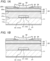
- a light-emitting element of the first embodiment or a second embodiment and a third embodiment described below is a surface emitting laser element (vertical resonator laser, VCSEL), specifically, and includes at least
- an off angle of the plane orientation of the crystal plane of a surface 11a of the GaN substrate 11 is 0.4 degrees or less, and preferably, 0.40 degrees or less, and when the area of the GaN substrate 11 is defined as S 0 , the area of the first light reflecting layer 41 is 0.004S 0 to 0.8S 0 . It should be noted that as the lower limit value of the area of the first light reflecting layer 41, 0.004 ⁇ S 0 is given.
- the plane orientation of the crystal plane of the surface 11a of the GaN substrate 11 was set to [0001] .
- the first light reflecting layer 41 and the layered structure 20 are formed on the (0001) plane (Cplane) of the GaN substrate 11, the first light reflecting layer 41 and the layered structure 20 are formed.
- a thermal expansion relaxation film 44 is formed on the GaN substrate 11, and the linear thermal expansion coefficient (CTE) of the bottom layer 41A (thermal expansion relaxation film 44 corresponds thereto) of the first light reflecting layer 41, in contact with the GaN substrate 11, satisfies 1 ⁇ 10 ⁇ 6 / K ⁇ CTE ⁇ 1 ⁇ 10 ⁇ 5 / K , preferably 1 ⁇ 10 ⁇ 6 / K ⁇ CTE ⁇ 1 ⁇ 10 ⁇ 5 / K .
- CTE values of silicon nitride (SiN X ) and the GaN substrate 11 are as shown in Table 1 below.
- the CTE values are values at 25°C.
- GaN substrate 5.59 ⁇ 10 -6 /K
- silicon nitride (SiN X ) 2.6 to 3.5 ⁇ 10 -6 /K
- the layered structure 20 is configured of the first compound semiconductor layer 21, the active layer 23, and the second compound semiconductor layer 22, more specifically, it is configured such that
- the light-emitting element is of second light reflecting layer emission type in which light is emitted from the second face 22b of the second compound semiconductor layer 22 via the second light reflecting layer 42.
- the GaN substrate 11 remains.
- a current constriction layer 24 made of an insulating material such as SiO X , SiN X , or AlO X is formed between the first electrode 32 and the second compound semiconductor layer 22.
- the current constriction layer 24 has an opening 24A, and the second compound semiconductor layer 22 is exposed to the bottom of the opening 24A.
- the first electrode 32 is formed on the second face 22b of the second compound semiconductor layer 22 over the current constriction layer 24, and the second light reflecting layer 42 is formed on the first electrode 32. Further, on the edge portion of the first electrode 32, a pad electrode 33 for electrical connection with an external electrode or a circuit is connected.
- the planar shape of the element region is a regular hexagonal shape
- the planar shapes of the first light reflecting layer 41, the second light reflecting layer 42, and the opening 24A formed in the current constriction layer 24 are circular shapes .
- each of the first light reflecting layer 41 and the second light reflecting layer 42 has a multilayer structure, it is shown as one layer in order to simplify the drawings. It should be noted that formation of the current constriction layer 24 is optional.
- a distance from the first light reflecting layer 41 to the second light reflecting layer 42 is 0.15 um or more but 50 um or less, and specifically, it is 10 ⁇ m, for example.
- the first compound semiconductor layer 21 is configured of an n-type GaN layer having a thickness of 5 um, and the active layer 23 having the entire thickness of 180 nm is formed of a five-tired multiple quantum well structure in which an In 0 . 04 Ga 0.96 N layer (barrier layer) and an In 0.16 Ga 0.84 N layer (well layer) are layered.
- the second compound semiconductor layer 22 has a double-layered configuration of a p-type AlGaN electron barrier layer (10 nm thick) and a p-type GaN layer. It should be noted that the electron barrier layer is located on the active layer side.
- the second electrode 31 is made of Ti/Pt/Au
- the first electrode 32 is made of a transparent conductive material, that is, ITO
- the pad electrode 33 is made of Ti/Pd/Au or Ti/Pt/Au
- the first light reflecting layer 41 and the second light reflecting layer 42 are configured of a layered structure of a SiN X layer and a SiO Y layer (the total number of layered dielectric films: 20 layers).
- the thickness of each layer is ⁇ 0 /(4n).
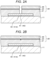
- a light-emitting element manufacturing method according to the first embodiment will be described with reference to Fig. 4A, Fig. 4B, and Fig. 4C each of which is a schematic partial end view of a layered structure or the like.
- the selective growth mask layer 43 is formed on the GaN substrate 11. Specifically, on the GaN substrate 11, the thermal expansion relaxation film 44 constituting the bottom layer of the selective growth mask layer 43 is formed, and further, on the thermal expansion relaxation film 44, the remaining part (functioning as the first light reflecting layer 41) of the selective growth mask layer 43, formed of the multilayer film, is formed. Then, the selective growth mask layer 43 is patterned. In this way, the structure shown in Fig. 4A can be obtained. As shown in Fig. 9 illustrating a schematic plan view, the shape of the selective growth mask layer 43 including the thermal expansion relaxation film 44 is a regular hexagonal shape. However, the shape of the selective growth mask layer 43 is not limited to this.
- the selective growth mask layer 43 is hatched to clearly show the selective growth mask layer 43. Between the selective growth mask layer 43 and the selective growth mask layer 43, the GaN substrate 11 is exposed.
- the first compound semiconductor layer 21 is selectively grown from the surface of the GaN substrate 11 not covered with the selective growth mask layer 43, and the GaN substrate 11 and the selective growth mask layer 43 are covered with the first compound semiconductor layer 21.
- the GaN substrate 11 is heated up to 1000°C while supplying ammonia gas using a MOCVD device, and then, by using a method of allowing epitaxial growth in the lateral direction such as an ELO method based on the MOCVD method using TMG gas and SiH 4 gas, the first compound semiconductor layer 21 is grown in the lateral direction.
- the active layer 23, the second compound semiconductor layer 22, the first electrode 32, and the second light reflecting layer 42 are sequentially formed on the first compound semiconductor layer 21.
- the temperature of the GaN substrate 11 is made 950°C, and an electron barrier layer is formed using TMG gas, TMA gas, Cp 2 Mg gas, and a p-type GaN layer is formed using TMG gas and Cp 2 Mg gas, to thereby obtain the second compound semiconductor layer 22.
- the layered structure 20 can be obtained. This means that on the GaN substrate 11 including the selective growth mask layer 43, the layered structure 20, in which
- the first electrode 32 and the second light reflecting layer 42 formed of the multilayer film are formed on the second face 22b of the second compound semiconductor layer 22, and further, the pad electrode 33 is formed on the first electrode 32 over the current constriction layer 24 by a well-known method. In this way, the structure shown in Fig. 4C can be obtained.
- the second light reflecting layer 42 is formed on the first electrode 32 over the pad electrode 33 on the basis of a well-known method.
- the second electrode 31 is formed on the basis of a well-known method. In this way, the structure shown in Fig. 1A can be obtained.
- the light-emitting element is separated by performing so-called element isolation, and side faces and an exposed face of the layered structure are covered with, for example, an insulating film made of SiO X .
- terminals or the like for connecting the second electrode 31 and the pad electrode 33 with an external circuit and the like are formed on the basis of a well-known method, and packaging and sealing are performed to complete the light-emitting element of the first embodiment.
- the surface roughness Ra of the second compound semiconductor layer 22 is preferably 1.0 nm or less.
- the selective growth mask layer 43 was peeled off from the GaN substrate 11 during deposition of the layered structure. Meanwhile, in the first embodiment, the selective growth mask layer 43 was not peeled off from the GaN substrate 11 during deposition of the layered structure.
- the off angle of the plane orientation of the crystal plane of the GaN substrate surface, and the area ratio of the selective growth mask layer (first light reflecting layer) are defined, it is possible to reduce the surface roughness of the second compound semiconductor layer. This means that it is possible to form a second compound semiconductor layer having excellent surface morphology. Consequently, as it is possible to obtain a second light reflecting layer having excellent smoothness, desired optical reflectance can be obtained, and variations in the characteristics of the light-emitting element are less likely to be caused.
- the thermal expansion relaxation film is formed or the value of CTE is defined, it is possible to prevent occurrence of a problem that the selective growth mask layer is peeled off from the GaN substrate due to a difference between the linear thermal expansion coefficient of the GaN substrate and the linear thermal expansion coefficient of the selective growth mask layer, whereby a light-emitting element having high reliability can be provided.
- a GaN substrate is used, dislocation is less likely to be caused in the compound semiconductor layer, and it is possible to prevent a problem that the heat resistance of the light-emitting element increases. As such, it is possible to give high reliability to the light-emitting element, and to provide an n-side electrode on a side different from the side of a p-side electrode with reference to the GaN substrate.
- the sectional shape of the selective growth mask layer 43 is a rectangle, it is not limited to this. It may be a trapezoid as shown in Fig. 1B .
- the selective growth mask layer 43 or the first light reflecting layer 41
- a portion of the selective growth mask layer 43 (or the first light reflecting layer 41) may be in an exposed state (see Fig. 2A ), or the first compound semiconductor layer 21 on the selective growth mask layer 43 (or the first light reflecting layer 41) may be in a state where it is not completely flat (see Fig. 2B ). It should be noted that in Fig.
- the current constriction layer 24, the first electrode 32, the pad electrode 33, the second light reflecting layer 42, and the second electrode 31 are not shown. It is only necessary that the light-emitting element is fabricated avoiding the region where the selective growth mask layer 43 (or the first light reflecting layer 41) is exposed or the region where the first compound semiconductor layer 21 is not completely flat. Specifically, it is preferable to apply the second embodiment described below. Further, as shown in Fig. 3 , the top layer (the layer in contact with the first compound semiconductor layer 21) 41B of the first light reflecting layer 41 may be formed of a silicon nitride film.
- t 2 ⁇ 0 / 4 n 2
- t 2 represents a thickness of the top layer 41B of the first light reflecting layer 41
- n 2 represents refractive index of the top layer 41B of the first light reflecting layer 41
- the first compound semiconductor layer 21 is formed by lateral overgrowth with use of a method of allowing epitaxial growth in the lateral direction such as an ELO method, if the first compound semiconductor layer 21 epitaxially growing from the edge portion of the selective growth mask layer 43 toward the center portion of the selective growth mask layer 43 associates, a large number of crystal defects may be caused in the associated portion.
- a method of allowing epitaxial growth in the lateral direction such as an ELO method
- an area centroid point of the second light reflecting layer 42 is not present on the normal line NL 1 with respect to the first light reflecting layer 41 passing through the area centroid point of the first light reflecting layer 41.
- an area centroid point of the active layer 23 is not present on the normal line NL 1 with respect to the first light reflecting layer 41 passing through the area centroid point of the first light reflecting layer 41.
- an associated portion in which a large number of crystal defects are present (specifically, located on the normal line NL 1 or in the vicinity thereof) is not located in the center portion of the element region, the characteristics of the light-emitting element are not adversely affected, or adverse effects on the characteristics of the light-emitting element are reduced.
- a third embodiment is a modification of the first embodiment and the second embodiment.
- Fig. 6A illustrating a schematic partial sectional view
- the light-emitting element of the third embodiment specifically, light generated in the active layer 23 is emitted to the outside from the top face of the first compound semiconductor layer 21 via the first light reflecting layer 41.
- the light-emitting element of the third embodiment formed of a surface emitting laser element (vertical resonator laser, VCSEL) is a light-emitting element of first light reflecting layer emission type.
- the second light reflecting layer 42 is fixed to a supporting substrate 26, configured of a silicon semiconductor substrate, on the basis of a solder joining method via a junction layer 25 formed of a solder layer including a gold (Au) layer or tin (Sn).
- the GaN substrate 11 is removed while using the first light reflecting layer 41 as a stopper layer.
- the active layer 23, the second compound semiconductor layer 22, the first electrode 32, and the second light reflecting layer 42 are sequentially formed on the first compound semiconductor layer 21, and then, after fixing the second light reflecting layer 42 to the supporting substrate 26, the GaN substrate 11 is removed with use of the first light reflecting layer 41 as a stopper layer, whereby the first compound semiconductor layer 21 (first face of the first compound semiconductor layer 21) and the first light reflecting layer 41 are exposed.
- the second electrode 31 is formed on the first compound semiconductor layer 21 (first face of the first compound semiconductor layer 21).
- a distance from the first light reflecting layer 41 to the second light reflecting layer 42 is 0.15 um or more but 50 um or less, and specifically, it is 10 ⁇ m, for example.
- the first light reflecting layer 41 and the second electrode 31 separate from each other, that is, they have an offset, and the separated distance is 1 mm or less, and specifically, an average thereof is 0.05 mm.
- a light-emitting element manufacturing method of the third embodiment will be described with reference to Fig. 7A and Fig. 7B each illustrating a schematic partial end view of a layered structure and the like.
- the structure shown in Fig. 1A is obtained by performing steps similar to [step-100] to [step-120] of the first embodiment, provided that the second electrode 31 is not formed.
- the second light reflecting layer 42 is fixed to the supporting substrate 26 via the junction layer 25. In this way, the structure shown in Fig. 7A can be obtained.
- the GaN substrate 11 is removed to expose the first face 21a of the first compound semiconductor layer 21 and the first light reflecting layer 41. Specifically, first, the thickness of the GaN substrate 11 is reduced on the basis of a mechanical polishing method, and then, on the basis of a CMP method, the remaining portion of the GaN substrate 11 is removed. In this way, the first face 21a of the first compound semiconductor layer 21 and the first light reflecting layer 41 are exposed, whereby the structure shown in Fig. 7B can be obtained.
- the second electrode 31 is formed on the first face 21a of the first compound semiconductor layer 21 on the basis of a well-known method. In this way, the light-emitting element of the third embodiment having the structure shown in Fig. 6A can be obtained.
- the light-emitting element is separated, and the side faces of the layered structure and the exposed faces are covered with an insulating film made of SiO X , for example.
- terminals and the like are formed on the basis of a well-known method in order to connect the second electrode 31 and the pad electrode 33 with an external circuit or the like, and packaging and sealing are performed, whereby the light-emitting element of the third embodiment is completed.
- the GaN substrate is removed in a state where the first light reflecting layer is formed.
- the first light reflecting layer functions as a kind of stopper when the GaN substrate is removed, it is possible to suppress occurrence of variations in removal of the GaN substrate in the GaN substrate surface, and further, variations in the thickness of the first compound semiconductor layer, whereby the length of the resonator can be uniform. Consequently, it is possible to achieve stability of the characteristics of the light-emitting element obtained.
- the surface of the first compound semiconductor layer (flat surface) on the interface between the first light reflecting layer and the first compound semiconductor layer is flat, it is possible to minimize light scattering on the flat surface.
- an end of the second electrode 31 is separated from the first light reflecting layer 41. Meanwhile, in the exemplary light-emitting element shown in Fig. 6B , an end of the second electrode 31 extends to the outer periphery of the first light reflecting layer 41.
- the second electrode may be formed such that an end of the second electrode is brought into contact with the first light reflecting layer.
- the present disclosure has been described above on the basis of preferable embodiments, the present disclosure is not limited to these embodiments.
- the configurations and the structures of the light-emitting elements described in the embodiments are exemplarily shown, which can be changed appropriately, and the light-emitting element manufacturing methods of the embodiments can also be changed appropriately.
- Fig. 8A illustrating a schematic partial sectional view of an exemplary modification of the light-emitting element of the first embodiment
- the bottom layer of the selective growth mask layer or the bottom layer of the first light reflecting layer may have a larger planar shape than that of a layer above the bottom layer.
- one light-emitting element is provided with one selective growth mask layer 43 (first light reflecting layer 41)
- the present disclosure is not limited to such a configuration.
- Fig. 8B illustrating a schematic partial sectional view of an exemplary modification of the light-emitting element of the first embodiment
- a configuration in which one light-emitting element is provided with a plurality of selective growth mask layers 43 and one of them is allowed to function as the first light reflecting layer 41, is also acceptable.
Description
- The present disclosure relates to a light-emitting element (specifically, a surface emitting laser element also called a vertical resonator laser, VCSEL), and a manufacturing method thereof.
- In a surface emitting laser element, laser oscillation is generally caused by oscillating light between two light reflection layers (distributed Bragg reflector layers, DBR layers). Accordingly, it is necessary to smooth a semiconductor surface for forming a DBR layer in sub-nanometer order. When an appropriate smoothness cannot be obtained, optical reflectance of each DBR layer is lowered, and variations in the characteristics (oscillation threshold and the like) are increased, which eventually makes it difficult to even obtain laser oscillation.
- A method of manufacturing a nitride surface emitting laser using a selective growth method is known from
Japanese Patent Application Laid-Open No. 10-308558 - a step of selectively forming a multilayer film made of dielectric on a substrate surface,
- a step of growing a nitride semiconductor layer on top of the multilayer film,
- a step of growing a nitride semiconductor layer including an active layer on top of the nitride semiconductor layer formed on top of the multilayer film, and
- a step of using the multilayer film as at least one reflecting mirror for light emission of the active layer.
-
Patent Document 2 discloses a nitride semiconductor light emitting device including a nitride semiconductor underlayer grown on a surface of a nitride semiconductor substrate or a surface of a nitride semiconductor substrate layer laminated over a base substrate of other than a nitride semiconductor, and a light emitting device structure having a light emitting layer including a quantum well layer or a quantum well layer and a barrier layer in contact with the quantum well layer between an n type layer and a p type layer over the nitride semiconductor underlayer. It includes a depression not flattened on a surface of the light emitting device structure even after growth of the light emitting device structure. - Publication 1 discloses highly reflective AlN/GaN and ZrO2-SiO2 multilayer reflectors and their applications for InGaN/GaN surface emitting laser structures. Design and fabrication of multilayer distributed Bragg reflectors (DBRs) for GaN based VCSELs covering firom ultra-violet to blue spectral region is present. In addition, a resonant emission from a photo-pumped InGaN/GaN vertical cavity structure with a cavity length of 1.9 um is demonstrated.
-
- Patent Document 1:
Japanese Patent Application Laid-Open No. 10-308558 - Patent Document 2:
US 2004/041156 A1 - Publication 1: SAKAGUCHI T ET AL: "Highly reflective AlN-GaN and ZrO2-SiO2 multilayer reflectors and their applications for InGaN-GaN surface emitting laser structures", LASERS AND ELECTRO-OPTICS SOCIETY ANNUAL MEETING, 1998. LEOS '98. IEEE ORLANDO, FL, USA 1-4 DEC. 1998, PISCATAWAY, NJ USA, IEEE, US, vol. 1,1 December 1998 (1998-12-01), pages 34-35
- Meanwhile, in the method of manufacturing a nitride semiconductor laser element disclosed in the laid-open patent application described above, a substrate different from a nitride semiconductor is used. However, in the case of using such a substrate, specifically, when a sapphire substrate is used, for example, a large number of dislocations occur due to lattice mismatch between a GaN-based compound semiconductor layer and a sapphire substrate, which gives significant adverse effects on the reliability of the light-emitting element. Further, as a sapphire substrate has lower heat conductivity than that of a typical semiconductor substrate, the heat resistance of the light-emitting element becomes extremely large, which causes an increase in the oscillation threshold electric current, a drop in the optical output, deterioration of the element service life, and the like. In addition, as a sapphire substrate does not have electrical conductivity, an n-side electrode cannot be provided to the rear face of the substrate, and an n-side electrode must be provided to the same side as that of a p-side electrode. As such, the element area increases, so that there is a problem that the productivity is poor. Further, the laid-open patent application described above fails to describe problems of peeling off of a multilayer film (selective growth mask layer) from a substrate due to a difference between a linear thermal expansion coefficient of the substrate and a linear thermal expansion coefficient of the multilayer film (selective growth mask layer), and variations in the characteristics (for example, variations in the optical reflectance) due to roughness of a surface of a nitride semiconductor layer when the nitride semiconductor layer including an active layer is grown, for example.
- Accordingly, an object of the present disclosure is to provide a light-emitting element in which variations in the characteristics are less likely to be caused, which has high reliability, and which is capable of preventing occurrence of a problem of peeling off of a selective growth mask layer from a substrate due to a difference between a linear thermal expansion coefficient of the substrate and a linear thermal expansion coefficient of a selective growth mask layer, and to provide a method of manufacturing the same.
- The invention is set out in the appended set of claims.
- With respect to the light-emitting element manufacturing method according a first aspect of the present disclosure,first electrode it should be noted that the selective growth mask layer may be covered entirely with the first compound semiconductor layer, or the selective growth mask layer may be covered partially. Further, the top face of the first compound semiconductor layer covering the selective growth mask layer may be flat, or may have a dent in a portion.
- Then, in the light-emitting element manufacturing method according to the first aspect of the present disclosure, a linear thermal expansion coefficient (CTE) of the bottom layer of the selective growth mask layer in contact with the GaN substrate may satisfy

first electrode - Further, in the light-emitting element of the present disclosure, a linear thermal expansion coefficient (CTE) of the bottom layer of first light reflecting layer in contact with the GaN substrate may satisfy

- In the light-emitting element and the manufacturing method thereof according to the first aspect and the second aspect of the present disclosure, as an off angle of the plane orientation of the surface of the GaN substrate and the area ratio of the selective growth mask layer (first light reflecting layer) are defined, it is possible to reduce the surface roughness of the second compound semiconductor layer. This means that it is possible to form a second compound semiconductor layer having excellent surface morphology. As such, it is possible to obtain a second light reflecting layer having excellent smoothness, that is, desired optical reflectance can be obtained, and variations in the characteristics of the light-emitting element are less likely to be caused. In addition, as a thermal expansion relaxation film is formed or a value of CTE is defined, it is possible to prevent occurrence of a problem that the selective growth mask layer is peeled off from the GaN substrate due to a difference between the linear thermal expansion coefficient of the GaN substrate and the linear thermal expansion coefficient of the selective growth mask layer, whereby a light-emitting element having high reliability can be provided. Further, as a GaN substrate is used, dislocation is less likely to be caused in the compound semiconductor layer, and it is possible to prevent a problem that heat resistance of the light-emitting element increases. As such, it is possible to give high reliability to the light-emitting element, and to provide an n-side electrode on a side different from the side of a p-side electrode with reference to the GaN substrate . It should be noted that the effects described in the present description are provided exemplarily without any limitation, and additional effects are also acceptable.
-
-
Fig. 1A and Fig. 1B are schematic partial sectional views of a light-emitting element and an exemplary modification of a first embodiment. -
Fig. 2A and Fig. 2B are schematic partial sectional views of other exemplary modifications of the light-emitting element of the first embodiment. -
Fig. 3 is a schematic partial sectional view of still another exemplary modification of the light-emitting element of the first embodiment. -
Fig. 4A, Fig. 4B, and Fig. 4C are schematic partial end views of a layered structure and the like for explaining a light-emitting element manufacturing method of the first embodiment. -
Fig. 5 is a schematic partial sectional view of a light-emitting element of a second embodiment. -
Fig. 6A and Fig. 6B are schematic partial sectional views of a light-emitting element and an exemplary modification of a third embodiment. -
Fig. 7A and Fig. 7B are schematic partial end views of a layered structure and the like for explaining a light-emitting element manufacturing method of the third embodiment. -
Fig. 8A and Fig. 8B are schematic partial sectional views of still other exemplary modifications of the light-emitting element of the first embodiment. -
Fig. 9 shows schematic plan views of selective growth mask layers. - Hereinafter, while the present disclosure is described on the basis of embodiments with reference to the drawings, the present disclosure is not limited to the embodiments. Various numerical values and materials described in the embodiments are exemplarily shown. It should be noted that the description will be given in the following order:
- 1. Overall description of light-emitting elements according to a first aspect and a second aspect of the present disclosure, and light-emitting element manufacturing methods according to the first aspect and the second aspect of the present disclosure
- 2. First embodiment (the light-emitting elements according to the first aspect and the second aspect of the present disclosure, and the light-emitting element manufacturing methods according to the first aspect and the second aspect of the present disclosure)
- 3. Second embodiment (a modification of the first embodiment)
- 4. Third embodiment (another modification of the first embodiment), and the like
- [Overall description of light-emitting elements according to a first aspect and a second aspect of the present disclosure, and light-emitting element manufacturing methods according to the first aspect and the second aspect of the present disclosure]
- A light-emitting element according to a first aspect of the present disclosure or a light emitting element obtained by a light-emitting element manufacturing method according to the first aspect of the present disclosure may collectively be referred to as "a light-emitting element and the like according to the first aspect of the present disclosure". Further, a light-emitting element according to a second aspect of the present disclosure or a light emitting element obtained by a light-emitting element manufacturing method according to the second aspect of the present disclosure may collectively be referred to as "a light-emitting element and the like according to the second aspect of the present disclosure". A face of a first compound semiconductor layer opposing an active layer may be called a second face of the first compound semiconductor layer, and a face of the first compound semiconductor layer opposing the second face of the first compound semiconductor layer may be called a first face of the first compound semiconductor layer. A face of a second compound semiconductor layer opposing the active layer may be called a first face of the second compound semiconductor layer, and a face of the second compound semiconductor layer opposing the first face of the second compound semiconductor layer may be called a second face of the second compound semiconductor layer.
- An off angle in the plane orientation of a surface of a GaN substrate indicates an angle defined by the plane orientation of a crystal plane of the surface of the GaN substrate and a normal line of the surface of the GaN substrate when viewed macroscopically. Further, in the light-emitting element manufacturing methods according to the first aspect and the second aspect of the present disclosure, assuming that the area of the GaN substrate is S0, it is defined that the area of a selective growth mask layer is 0.004S0 to 0.8S0, and in the light-emitting elements according to the first aspect and the second aspect of the present disclosure, assuming that the area of the GaN substrate is S0, it is defined that the area of a first light reflecting layer is 0.004S0 to 0.8S0. However, "the area S0 of the GaN substrate" indicates the area of the GaN substrate remained when a light-emitting element is finally obtained. A bottom layer of the selective growth mask layer or a bottom layer of the first light reflecting layer does not have a function as a light reflecting layer.
- In the light-emitting element and the like according to the first aspect of the present disclosure, a thermal expansion relaxation film may be in a mode made of at least one type of material selected from the group consisting of silicon nitride (SiNX), aluminum oxide (AlOX), niobium oxide (NbOX), tantalum oxide (TaOX), titanium oxide (TiOX), magnesium oxide (MgOX), zirconium oxide (ZrOX), and aluminum nitride (AlNX). It shouldbe noted that a value of a suffix "X" attached to the chemical formula for each of the substances, or a suffix "Y" or a suffix "Z", described below, includes not only a value based on the stoichiometry of each material but also a value deviated from a value based on the stoichiometry. This is similar in the below description. Then, in the light-emitting element and the like according to the first aspect of the present disclosure including such a preferable mode, it is desirable to satisfy

- In the light-emitting element and the like according to the second aspect of the present disclosure, a bottom layer of the selective growth mask layer (first light reflecting layer) may be in a mode made of at least one type of material selected from the group consisting of silicon nitride (SiNX), aluminum oxide (AlOX), niobium oxide (NbOX), tantalum oxide (TaOX), titanium oxide (TiOX), magnesium oxide (MgOX), zirconium oxide (ZrOX), and aluminum nitride (AlNx). Then, in the light-emitting element and the like according to the second aspect of the present disclosure including such a preferable mode, it is desirable to satisfy

- In the light-emitting element manufacturing methods according to the first aspect and the second aspect of the present disclosure including various preferable modes described above, the GaN substrate may remain, or the GaN substrate may be removed after forming, the active layer, the second compound semiconductor layer, a first electrode, and a second light reflecting layer, sequentially on the first compound semiconductor layer, with the first light reflecting layer being used as a stopper layer. Specifically, the active layer, the second compound semiconductor layer, the first electrode, and the second light reflecting layer are formed sequentially on the first compound semiconductor layer, and after the second light reflecting layer is fixed to the supporting substrate, the GaN substrate is removed with the first light reflecting layer being used as the stopper layer, whereby the first compound semiconductor layer (first face of the first compound semiconductor layer) and the first light reflecting layer may be exposed. Further, a second electrode may be formed on the first compound semiconductor layer (first face of the first compound semiconductor layer).
- Removal of the GaN substrate may be in a mode in which it is performed on the basis of a chemical/mechanical polishing method (CMP method) . It should be noted that first, a part of the GaN substrate may be removed, or the thickness of the GaN substrate may be reduced, by means of a wet etching method using alkali aqueous solution such as aqueous sodium hydroxide solution or aqueous potassium hydroxide solution, ammonia solution + hydrogen peroxide solution, sulphuric acid solution + hydrogen peroxide solution, hydrochloric acid solution + hydrogen peroxide solution, phosphoric acid solution + hydrogen peroxide solution, or the like, a dry etching method, a lift-off method using laser, a mechanical polishing method or the like, or a combination thereof, and then, the first compound semiconductor layer (first face of the first compound semiconductor layer) and the first light reflecting layer may be exposed by performing a chemical/mechanical polishing method.
- Furthermore, in the light-emitting element and the like according to the first aspect and the second aspect of the present disclosure including various preferable modes described above, the surface roughness Ra of the second compound semiconductor layer (second face of the second compound semiconductor layer) is preferably 1.0 nm or less. The surface roughness Ra is defined in JIS B-610:2001, and specifically, it can be measured on the basis of observation based on AFM or sectional TEM.
- Further, in the light-emitting element and the like according to the first aspect and the second aspect of the present disclosure including various preferable modes described above, a planar shape of the selective growth mask layer (or the first light reflecting layer) may be in a mode of any of various polygonal shapes including a regular hexagonal shape, a circular shape, an oval shape, a lattice shape (rectangle), an island-like shape, or a stripe shape. While a sectional shape of the selective growth mask layer (or the first light reflecting layer) may be a rectangular shape, it is more preferable that it is a trapezoidal shape, that is, a side face of the selective growth mask layer (or the first light reflecting layer) is in a forward tapered shape. As a method of forming the selective growth mask, a combination of physical vapor deposition method (PVD method) such as sputtering, chemical vapor deposition method (CVD), or a paint-on method, and a lithography technique or an etching technique, may be given.
- It is preferable to satisfy


- In the light-emitting element and the like according to the present disclosure including various prefer able modes described above, a distance from the first light reflecting layer to the second light reflecting layer is preferably 0.15 um or more but 50 um or less.
- Further, in the light-emitting element and the like according to the present disclosure including various prefer able modes described above, a mode, in which an area centroid point of the second light reflecting layer is not present on a normal line with respect to the first light reflecting layer passing through the area centroid point of the first light reflecting layer, is acceptable.
- Furthermore, in the light-emitting element and the like according to the first aspect or the second aspect of the present disclosure including various prefer able modes described above, a mode, in which an area centroid point of the active layer is not present on a normal line with respect to the first light reflecting layer passing through the area centroid point of the first light reflecting layer, is acceptable.
- When the first compound semiconductor layer is formed, on the GaN substrate where the selective growth mask layer is formed, by lateral overgrowth with use of a method allowing epitaxial growth in a lateral direction such as an epitaxial lateral overgrowth (ELO) method, when the first compound semiconductor layer growing epitaxially toward the center portion of the selective growth mask layer from an edge portion of the selective growth mask layer associates, there is a case where a large amount of crystal defect occurs at the associated portion. When the associated portion where a large amount of crystal defect exists is located at a center portion of an element region (to be described below), the characteristic of the light-emitting element may be adversely affected. As described above, with the mode in which the area centroid point of the second light reflecting layer is not present on the normal line with respect to the first light reflecting layer passing through the first light reflecting layer, and the mode in which the area centroid point of the active layer is not present on the normal line with respect to the first light reflecting layer passing through the area centroid point of the first light reflecting layer, occurrence of an adverse effect on the characteristic of the light-emitting element can be prevented reliably.
- In the light-emitting element and the like according to the present disclosure including various prefer able modes described above, light generated in the active layer may be in a mode in which the light is emitted to the outside via the second light reflecting layer (hereinafter referred to as a"light-emitting element of second light reflecting layer emission type" for convenience) or may be in a mode in which the light is emitted to the outside via the first light reflecting layer (hereinafter referred to as a "light-emitting element of first light reflecting layer emission type" for convenience) . It should be noted that in the case of the light-emitting element of first light reflecting layer emission type, the GaN substrate may be removed as described above in some instances .
- Then, in the case of a light-emitting element of the first light reflecting layer emission type, it is desirable to satisfy


- Further, in the mode in which the area centroid point of the second light reflecting layer is not present on the normal line with respect to the first light reflecting layer passing through the area centroid point of the first light reflecting layer, and in the mode in which the area centroid point of the active layer is not present on the normal line with respect to the first light reflecting layer passing through the area centroid point of the first light reflecting layer, in the case of a light-emitting element of the first light reflecting layer emission type, it is desirable to satisfy


- In the light-emitting element of the first light reflecting layer emission type, in the case of removing the GaN substrate, the second light reflecting layer may be in a mode of being fixed to the supporting substrate. In the light-emitting element of the first light reflecting layer emission type, in the case of removing the GaN substrate, as an arrangement state of the first light reflecting layer and the second electrode on the first face of the first compound semiconductor layer, a state where the first light reflecting layer and the second electrode are in contact with each other may be given, or a state where the first light reflecting layer and the second electrode are separated from each other may be given, and in some instances, a state where the second electrode is formed on to the edge portion of the first light reflecting layer, or a state where the first light reflecting layer is formed on to the edge portion of the second electrode may be given. Here, in the case of a state where the first light reflecting layer is formed on to the edge portion of the second electrode, the second electrode needs to have an opening of a certain size so as not to absorb basic mode light of laser oscillation as much as possible. As the size of the opening varies according to a wavelength of the basic mode or a light confinement structure in the lateral direction (in-plane direction of the first compound semiconductor layer), it is preferable to be in about several times order of the emission wavelength λ0, although it is not limited to this. Alternatively, it is possible to have a configuration in which the first light reflecting layer and the second electrode are separated from each other, that is, having an offset, and the separated distance is 1 mm or less.
- Further, in the light-emitting element and the like according to the present disclosure including various prefer able modes described above, the second electrode may be in a mode of being made of metal or an alloy, and the first electrode may be in a mode of being made of a transparent conductive material. By making the first electrode from a transparent conductive material, an electric current can be expanded in the lateral direction (in-plane direction of the second compound semiconductor layer), and to supply the electric current to an element region (described subsequently) with high efficiency.
- An "element region" indicates a region where a constricted electric current is injected, or a region where light is confined by a refractive index difference or the like, or a region where laser oscillation is caused within a region sandwiched between the first light reflecting layer and the second light reflecting layer, or a region actually contributing to laser oscillation within a region sandwiched between the first light reflecting layer and the second light reflecting layer.
- As described above, the light-emitting element may be configured to be formed of a surface emitting laser element (vertical resonator laser, VCSEL) which emits light from the top face of the first compound semiconductor layer via the first light reflecting layer, or may be configured to be formed of a surface emitting laser element which emits light from the top face of the second compound semiconductor layer via the second light reflecting layer.
- In the light-emitting element and the like according to the first aspect and the second aspect of the present disclosure including various prefer able modes described above, a layered structure formed of the first compound semiconductor layer, the active layer, and the second compound semiconductor layer may be configured of a GaN-based compound semiconductor, specifically. Here, as a GaN-based compound semiconductor, more specifically, GaN, AlGaN, InGaN, or Al InGaN can be given. Further, such a compound semiconductor may contain a boron (B) atom, a thallium (Tl) atom, an arsenic (As) atom, a phosphorus (P) atom, or an antimony (Sb) atom, as desired. It is desirable that the active layer has a quantum well structure. Specifically, it may have a single quantum well structure (QW structure) or a multiple quantum well structure (MQW structure) . While an active layer having a quantum well structure has a structure in which at least one layer of a well layer and at least one layer of a barrier layer are layered, as a combination of (a compound semiconductor constituting the wall layer, and a compound semiconductor constituting a barrier layer), (InyGa(1-y)N, GaN), (InyGa(1-y)N, InzGa(1-z)N) [provided that y > z], or (InyGa(1-y)N, AlGaN) maybe exemplarily shown. The first compound semiconductor layer can be configured of a compound semiconductor of a first conductive-type (n-type, for example), and the second compound semiconductor layer can be configured of a compound semiconductor of a second conductive-type (p-type, for example) which is different from the first conductive type. The first compound semiconductor layer and the second compound semiconductor layer are also called a first cladding layer and a second cladding layer. It is desirable that a current constriction structure is formed between the first electrode and the second compound semiconductor layer. The first compound semiconductor layer and the second compound semiconductor layer each may be a layer of a single structure, a layer of a multiple structure, or a layer of a superlattice structure. Further, it may be a layer having a composition gradient layer or a concentration gradient layer.
- In order to obtain a current constriction structure, a current constriction layer made of an insulating material (SiOX, SiNX, or AlOX, for example) may be formed between the first electrode and the second compound semiconductor layer, or a mesa structure may be formed by performing etching on the second compound semiconductor layer by the RIE method or the like, or a current constriction region may be formed by partially oxidizing a portion of the layered second compound semiconductor layer from the lateral direction, or a region where the conductivity is lowered may be formed by ion-implanting impurity into the second compound semiconductor layer, or these may be combined appropriately. However, it is necessary that the first electrode is electrically connected with a portion of the second compound semiconductor layer where an electric current flows by the current constriction.
- While it has been known that the characteristic of a GaN substrate is changed to be polar/nonpolar/semi polar according to the growth face, any of the principal planes of a GaN substrate can be used for formation of a compound semiconductor layer. Further, regarding the principal planes of a GaN substrate, depending on the crystal structure (for example, cubic crystal type, hexagonal crystal type, or the like), a plane in which the plane orientation of a crystal plane referred to as a so-called A plane, B plane, C plane, R plane, M plane, N plane, S plane, or the like is made off in a particular direction (including the case where the off angle is 0 degrees) is used. Methods of forming various compound semiconductor layers for constituting a light-emitting element include an organic metal chemical vapor deposition method (MOCVD method, MOVPE method), a molecular beam epitaxy method (MBE method), a hydride vapor phase growing method in which halogen contributes to transportation or reaction, and the like may be given.
- Here, as an organic gallium source in a MOCVD method, trimethylgallium (TMG) or triethylgallium (TEG) may be given, and as nitrogen source gas, ammonia gas or hydrazine may be given. In formation of a GaN-based compound semiconductor layer having n-type conductivity, silicon (Si) may be added as n-type impurity (n-type dopant), for example, and in formation of a GaN-based compound semiconductor layer having p-type conductivity, magnesium (Mg) may be added as p-type impurity (p-type dopant), for example. In the case where aluminum (Al) or indium (In) is included as a configuration atom of a GaN-based compound semiconductor layer, trimethylaluminum (TMA) may be used as an Al source, and trimethylindium (TMI) may be used as an In source. Further, as an Si source, monosilane gas (SiH4 gas) may be used, and as a Mg source, bis (cyclopentadienyl) magnesium, methylcyclopentadienyl magnesium, bis (cyclopentadienyl) magnesium (Cp2Mg) may be used. It should be noted that as n-type impurity (n-type dopant), Ge, Se, Sn, C, Te, S, O, Pd, or Po may be given, besides Si, and as p-type impurity (p-type dopant), Zn, Cd, Be, Ca, Ba, C, Hg, or Sr may be given, besides Mg.
- The supporting substrate may be configured of any of various substrates such as a GaN substrate, a sapphire substrate, a GaAs substrate, a SiC substrate, an alumina substrate, a ZnS substrate, a ZnO substrate, a LiMgO substrate, a LiGaO2 substrate, a MgAl2O4 substrate, and an InP substrate, for example. Alternatively, it may also be configured of an insulating substrate made of AlN or the like, a semiconductor substrate made of Si, SiC, Ge, or the like, ametallic substrate, or a substrate made of an alloy. However, it is preferable to use a substrate having conductivity, or it is preferable to use a metal substrate or an alloy substrate from the viewpoint of mechanical characteristic, elastic deformation, plastic deformation, heat dissipation, and the like. As a thickness of the supporting substrate, a thickness of 0.05 mm to 0.5 mm may be exemplarily given, for example. As a method of fixing the second light reflecting layer to the supporting substrate, while any known method such as a solder joining method, a normal temperature joining method, a joining method using adhesive tape, or a joining method using wax joining, can be used, it is desirable to adopt a solder joining method or a normal temperature joining method from the viewpoint of ensuring conductivity. For example, in the case of using a silicon semiconductor substrate which is a conductive substrate as a supporting substrate, it is desirable to adopt a method capable of performing joining at a low temperature of 400°C or lower in order to suppress warpage caused by a difference in the thermal expansion coefficient. In the case of using a GaN substrate as a supporting substrate, the joining temperature may be 400°C or higher.
- The second electrode desirably has a single layer configuration or a multilayer configuration including at least one type of metal (including an alloy) selected from the group consisting of gold (Au), silver (Ag), palladium (Pd), platinum (Pt), nickel (Ni), Ti (titanium), vanadium (V), tungsten (W), chromium (Cr), aluminum (Al), copper (Cu), zinc (Zn), tin (Sn), and indium(In), for example. Specifically, Ti/Au, Ti/Al, Ti/Al/Au, Ti/Pt/Au, Ni/Au, Ni/Au/Pt, Ni/Pt, Pd/Pt, and Ag/Pd can be exemplarily shown, for example. It should be noted that a layer before "/" in a multilayer configuration is located closer to the active layer side. This is similar in the below description. The second electrode can be deposited by a PVD method such as a vacuum vapor deposition method or a sputtering method, for example.
- As a transparent conductive material constituting the first electrode, indium-tin oxide (ITO, including Sn-doped In2O3, crystalline ITO, and amorphous ITO), indium-zinc oxide (IZO), IFO (F-doped In2O3), tin oxide (SnO2), ATO (Sb-doped SnO2), FTO (F-doped SnO2), or zinc oxide (ZnO, including Al-doped ZnO and B-doped ZnO) can be given exemplarily. Alternatively, as the first electrode, a transparent conductive film in which the base layer is made of gallium oxide, titanium oxide, niobium oxide, nickel oxide, or the like can be given. However, as a material constituting the first electrode, while it depends on the arrangement state between the second light reflecting layer and the first electrode, it is not limited to a transparent conductive material. Metal such as palladium (Pd), platinum (Pt), nickel (Ni), gold (Au), cobalt (Co), or rhodium (Rh) can be used. The first electrode may be made of at least one type of these materials. The first electrode can be deposited by a PVD method such as a vacuum vapor deposition method, a sputtering method, or the like, for example.
- On the second electrode and the first electrode, a pad electrode may be provided for electrical connection with an external electrode or a circuit. It is desirable that a pad electrode has a single layer configuration or a multilayer configuration including at least one type of metal selected from the group consisting of Ti (titanium), aluminum (Al), platinum (Pt), gold (Au), nickel (Ni), and palladium (Pd). Alternatively, a pad electrode may have a multilayer configuration exemplarily given as a multilayer configuration of Ti/Pt/Au, a multilayer configuration of Ti/Au, a multilayer configuration of Ti/Pd/Au, a multilayer configuration of Ti/Pd/Au, a multilayer configuration of Ti/Ni/Au, a multilayer configuration of Ti/Ni/Au/Cr/Au. In the case where the second electrode is configured of an Ag layer or an Ag/Pd layer, it is preferable to form a cover metal layer made of Ni/TiW/Pd/TiW/Ni on the surface of the second electrode, for example, and on the cover metal layer, form a pad electrode formed of a multilayer configuration of Ti/Ni/Au or a multilayer configuration of Ti/Ni/Au/Cr/Au, for example.
- The light reflecting layer (Distributed Bragg Reflector layer, DBR layer) is configured of a semiconductor multilayer film or a dielectric multilayer film, for example. As a dielectric material, oxide such as Si, Mg, Al, Hf, Nb, Zr, Sc, Ta, Ga, Zn, Y, B, or Ti, nitride (for example, SiNX, AlNX, AlGaN, GaNX, BNX, or the like), fluoride, or the like may be given, for example. Specifically, SiOX, TiOX, NbOX, ZrOX, TaOX, ZnOX, AlOX, HfOX, SiNX, AlNX or the like may be exemplarily given. Then, by alternately layering two types or more dielectric films made of dielectric materials having different refractive indexes among the dielectric materials, a light reflecting layer can be obtained. For example, a multilayer film such as SiOX/SiNY, SiOX/NbOY, SiOX/ZrOY, SiOX/AlNY, or the like is preferable. In order to obtain a desired optical reflectance, materials for constituting each dielectric film, film thickness, the number of layers, and the like may be selected appropriately. The thickness of each dielectric film can be adjusted appropriately depending on the material to be used or the like, which is determined by the emission wavelength λ0 and the refractive index n at the emission wavelength λ0 of the material to be used. Specifically, it is preferable to be odd number times of λ0/(4n). For example, in the light-emitting element having the emission wavelength λ0 of 410 nm, when the light reflecting layer is configured of SiOX/NbOY, a thickness of about 40 nm to about 70 nm can be exemplarily given. As the number of layers, two, and preferably, from about five to about twenty can be exemplarily given. As the thickness of the entire light reflecting layer, a thickness of about 0.6 um to about 1.7 um can be exemplarily given.
- Alternatively, it is desirable that the first light reflecting layer has a dielectric film including at least a nitrogen (N) atom, and further, it is more desirable that the dielectric film including an N atom is the top layer of the dielectric multilayer film. Alternatively, it is desirable that the first light reflecting layer is covered by a dielectric material layer including at least a nitrogen (N) atom. Alternatively, it is desirable to apply nitriding treatment to the surface of the first light reflecting layer to thereby make the surface of the first light reflecting layer a layer including at least a nitrogen (N) atom (hereinafter referred to as "surface layer" for convenience) . It is preferable that the thickness of a dielectric film, a dielectric material layer, or the surface layer including at least an N atom is odd number times of λ0/(4n). As a material constituting a dielectric film or a dielectric material layer including at least an N atom, SiNX or SiOXNZ can be given, specifically. As described above, by forming a dielectric film, a dielectric material layer, or a surface layer including at least an N atom, when a compound semiconductor layer covering the first light reflecting layer is formed, it is possible to improve a gap between the crystal axis of the compound semiconductor layer covering the first light reflecting layer and the crystal axis of the GaN substrate, which enables the quality of the layered structure, serving as a resonator, to be enhanced.
- The light reflecting layer can be formed by a well-known method. Specifically, a PVD method such as a vacuum vapor deposition method, a sputtering method, a reactive sputtering method, anECRplasmasputteringmethod, amagnetron sputtering method, an ion beam assisted deposition method, an ion plating method, or a laser ablation method; any type of CVD method; a paint-on method such as a spraying method, a spin coating method, or a dip method; a method combining two types or more of these methods; a method combining any of these methods and any one or more types of overall or partial pre-processing, irradiation with inert gas (Ar, He, Xe, or the like) or plasma, irradiation with oxygen gas, ozone gas, or plasma, oxidation treatment (thermal treatment), and exposure processing, can be given.
- Further, side faces or exposed faces of the layered structure may be covered with an insulating film. An insulating film can be formed on the basis of a well-known method. It is preferable that the refractive index of a material constituting the insulating film is smaller than the refractive index of a material constituting the layered structure. As a material constituting the insulating film, a SiOX-based material including SiO2, a SiNX-based material, a SiOXNZ-based material, TaOX, ZrOX, AlNX, AlOX, or GaOX can be exemplarily given, or an organic material such as polyimide resin can be exemplarily given. As a method of forming the insulating film, a PVD method such as a vacuum vapor deposition method or a sputtering method, or a CVD method can be given, or it can be formed by a paint-on method.
- A first embodiment relates to the light-emitting elements according to the first aspect and second aspect of the present disclosure, and manufacturing methods thereof.
- As shown in
Fig. 1A illustrating a schematic partial side face, a light-emitting element of the first embodiment or a second embodiment and a third embodiment described below is a surface emitting laser element (vertical resonator laser, VCSEL), specifically, and includes at least - a
GaN substrate 11, - a first
light reflecting layer 41 formed on theGaN substrate 11 and functioning as a selectivegrowth mask layer 43, - a
layered structure 20 configured of a firstcompound semiconductor layer 21, anactive layer 23, and a secondcompound semiconductor layer 22 which are formed on the firstlight reflecting layer 41, and - a
first electrode 32 and a secondlight reflecting layer 42 formed on the secondcompound semiconductor layer 22. - Then, in the light-emitting element of the first embodiment or the second embodiment and the third embodiment described below, or in the light-emitting element manufacturing method, an off angle of the plane orientation of the crystal plane of a
surface 11a of theGaN substrate 11 is 0.4 degrees or less, and preferably, 0.40 degrees or less, and when the area of theGaN substrate 11 is defined as S0, the area of the firstlight reflecting layer 41 is 0.004S0 to 0.8S0. It should be noted that as the lower limit value of the area of the firstlight reflecting layer 41, 0.004 × S0 is given. Here, the plane orientation of the crystal plane of thesurface 11a of theGaN substrate 11 was set to [0001] . This means that on the (0001) plane (Cplane) of theGaN substrate 11, the firstlight reflecting layer 41 and thelayered structure 20 are formed. It should be noted that as abottom layer 41A of the firstlight reflecting layer 41, a thermalexpansion relaxation film 44 is formed on theGaN substrate 11, and the linear thermal expansion coefficient (CTE) of thebottom layer 41A (thermalexpansion relaxation film 44 corresponds thereto) of the firstlight reflecting layer 41, in contact with theGaN substrate 11, satisfies

- Specifically, the thermal expansion relaxation film 44 (the bottom layer of the selective growth mask layer 43) is formed of silicon nitride (SiNX) satisfying

GaN substrate 11 are as shown in Table 1 below. The CTE values are values at 25°C.[Table 1] GaN substrate : 5.59×10⁻⁶/K silicon nitride (SiNX) : 2.6 to 3.5×10⁻⁶/K - It should be noted that while the layered
structure 20 is configured of the firstcompound semiconductor layer 21, theactive layer 23, and the secondcompound semiconductor layer 22, more specifically, it is configured such that - the first
compound semiconductor layer 21 formed of a GaN-based compound semiconductor, and including afirst face 21a and asecond face 21b opposing thefirst face 21a, - the active layer (light emitting layer) 23 formed of a GaN-based compound semiconductor, and brought into contact with the
second face 21b of the firstcompound semiconductor layer 21, and - the second
compound semiconductor layer 22 formed of a GaN-based compound semiconductor, including afirst face 22a and asecond face 22b opposing thefirst face 22a, in which thefirst face 22a is brought into contact with theactive layer 23, are layered. Then, on thesecond face 22b of the secondcompound semiconductor layer 22, the secondlight reflecting layer 42, configured of thefirst electrode 32 and a multilayer film, is formed, and asecond electrode 31 is formed on anotherplane 11b of theGaN substrate 11 opposing thesurface 11a of theGaN substrate 11 on which the layeredstructure 20 is formed. The firstlight reflecting layer 41, configured of a multilayer film, is formed on thesurface 11a of theGaN substrate 11, and is formed in contact with thefirst face 21a of the firstcompound semiconductor layer 21. - Here, in the first embodiment, the light-emitting element is of second light reflecting layer emission type in which light is emitted from the
second face 22b of the secondcompound semiconductor layer 22 via the secondlight reflecting layer 42. TheGaN substrate 11 remains. - In the light-emitting element of the first embodiment or the second embodiment and the third embodiment described below, a
current constriction layer 24 made of an insulating material such as SiOX, SiNX, or AlOX is formed between thefirst electrode 32 and the secondcompound semiconductor layer 22. Thecurrent constriction layer 24 has anopening 24A, and the secondcompound semiconductor layer 22 is exposed to the bottom of theopening 24A. Thefirst electrode 32 is formed on thesecond face 22b of the secondcompound semiconductor layer 22 over thecurrent constriction layer 24, and the secondlight reflecting layer 42 is formed on thefirst electrode 32. Further, on the edge portion of thefirst electrode 32, apad electrode 33 for electrical connection with an external electrode or a circuit is connected. In the light-emitting element of the first embodiment or the second embodiment and the third embodiment described below, the planar shape of the element region is a regular hexagonal shape, and the planar shapes of the firstlight reflecting layer 41, the secondlight reflecting layer 42, and theopening 24A formed in thecurrent constriction layer 24 are circular shapes . It should be noted that while each of the firstlight reflecting layer 41 and the secondlight reflecting layer 42 has a multilayer structure, it is shown as one layer in order to simplify the drawings. It should be noted that formation of thecurrent constriction layer 24 is optional. - Then, in the light-emitting element of the first embodiment, a distance from the first
light reflecting layer 41 to the secondlight reflecting layer 42 is 0.15 um or more but 50 um or less, and specifically, it is 10 µm, for example. - The first
compound semiconductor layer 21 is configured of an n-type GaN layer having a thickness of 5 um, and theactive layer 23 having the entire thickness of 180 nm is formed of a five-tired multiple quantum well structure in which an In0.04Ga0.96N layer (barrier layer) and an In0.16Ga0.84N layer (well layer) are layered. The secondcompound semiconductor layer 22 has a double-layered configuration of a p-type AlGaN electron barrier layer (10 nm thick) and a p-type GaN layer. It should be noted that the electron barrier layer is located on the active layer side. Thesecond electrode 31 is made of Ti/Pt/Au, and thefirst electrode 32 is made of a transparent conductive material, that is, ITO, and specifically, thepad electrode 33 is made of Ti/Pd/Au or Ti/Pt/Au, and the firstlight reflecting layer 41 and the secondlight reflecting layer 42 are configured of a layered structure of a SiNX layer and a SiOY layer (the total number of layered dielectric films: 20 layers). The thickness of each layer is λ0/(4n). - Hereinafter, a light-emitting element manufacturing method according to the first embodiment will be described with reference to
Fig. 4A, Fig. 4B, and Fig. 4C each of which is a schematic partial end view of a layered structure or the like. - First, the selective
growth mask layer 43 is formed on theGaN substrate 11. Specifically, on theGaN substrate 11, the thermalexpansion relaxation film 44 constituting the bottom layer of the selectivegrowth mask layer 43 is formed, and further, on the thermalexpansion relaxation film 44, the remaining part (functioning as the first light reflecting layer 41) of the selectivegrowth mask layer 43, formed of the multilayer film, is formed. Then, the selectivegrowth mask layer 43 is patterned. In this way, the structure shown inFig. 4A can be obtained. As shown inFig. 9 illustrating a schematic plan view, the shape of the selectivegrowth mask layer 43 including the thermalexpansion relaxation film 44 is a regular hexagonal shape. However, the shape of the selectivegrowth mask layer 43 is not limited to this. It may be a circular shape, a lattice shape, or a stripe shape, for example. It should be noted that inFig. 9 , the selectivegrowth mask layer 43 is hatched to clearly show the selectivegrowth mask layer 43. Between the selectivegrowth mask layer 43 and the selectivegrowth mask layer 43, theGaN substrate 11 is exposed. - Next, the first
compound semiconductor layer 21 is selectively grown from the surface of theGaN substrate 11 not covered with the selectivegrowth mask layer 43, and theGaN substrate 11 and the selectivegrowth mask layer 43 are covered with the firstcompound semiconductor layer 21. Specifically, theGaN substrate 11 is heated up to 1000°C while supplying ammonia gas using a MOCVD device, and then, by using a method of allowing epitaxial growth in the lateral direction such as an ELO method based on the MOCVD method using TMG gas and SiH4 gas, the firstcompound semiconductor layer 21 is grown in the lateral direction. - Subsequently, with the temperature of the
GaN substrate 11 being 800°C, theactive layer 23, the secondcompound semiconductor layer 22, thefirst electrode 32, and the secondlight reflecting layer 42 are sequentially formed on the firstcompound semiconductor layer 21. Specifically, on the basis of the epitaxial growth method, after forming theactive layer 23 on the firstcompound semiconductor layer 21 using TMG gas and TMI gas, the temperature of theGaN substrate 11 is made 950°C, and an electron barrier layer is formed using TMG gas, TMA gas, Cp2Mg gas, and a p-type GaN layer is formed using TMG gas and Cp2Mg gas, to thereby obtain the secondcompound semiconductor layer 22. Through the above-described step, the layeredstructure 20 can be obtained. This means that on theGaN substrate 11 including the selectivegrowth mask layer 43, the layeredstructure 20, in which - the first
compound semiconductor layer 21 formed of a GaN-based compound semiconductor and including afirst face 21a and asecond face 21b opposing thefirst face 21a, - the
active layer 23 formed of a GaN-based compound semiconductor and brought into contact with thesecond face 21b of the firstcompound semiconductor layer 21, and - the second
compound semiconductor layer 22 formed of a GaN-based compound semiconductor and including afirst face 22a and asecond face 22b opposing thefirst face 22a, in which thefirst face 22a is brought into contact with theactive layer 23, are layered, is epitaxially grown. Then, on thesecond face 22b of the secondcompound semiconductor layer 22, thecurrent constriction layer 24, made of an insulating member of 0.2 um thick and having theopening 24A, is formed on the basis of a well-known method. In this way, the structure shown inFig. 4B can be obtained. - Then, on the
second face 22b of the secondcompound semiconductor layer 22, thefirst electrode 32 and the secondlight reflecting layer 42 formed of the multilayer film are formed. Specifically, on the basis of a lift-off method, for example, thefirst electrode 32 made of ITO of 50 nm thick is formed on thesecond face 22b of the secondcompound semiconductor layer 22 over thecurrent constriction layer 24, and further, thepad electrode 33 is formed on thefirst electrode 32 over thecurrent constriction layer 24 by a well-known method. In this way, the structure shown inFig. 4C can be obtained. Then, the secondlight reflecting layer 42 is formed on thefirst electrode 32 over thepad electrode 33 on the basis of a well-known method. Meanwhile, on theother surface 11b of theGaN substrate 11, thesecond electrode 31 is formed on the basis of a well-known method. In this way, the structure shown inFig. 1A can be obtained. - Then, the light-emitting element is separated by performing so-called element isolation, and side faces and an exposed face of the layered structure are covered with, for example, an insulating film made of SiOX. Then, terminals or the like for connecting the
second electrode 31 and thepad electrode 33 with an external circuit and the like are formed on the basis of a well-known method, and packaging and sealing are performed to complete the light-emitting element of the first embodiment. - In the first embodiment, a relationship between the off angle and the surface roughness Ra of the second
compound semiconductor layer 22 was examined. The results are shown in Table 2 provided below. It is found from Table 2 that when the off angle exceeds 0.4 degrees, the value of the surface roughness Ra of the secondcompound semiconductor layer 22 increases. As such, by setting the off angle to be 0.4 degrees or less, and preferably, 0.40 degrees or less, a step bunching of the growing compound semiconductor layer can be suppressed, and it is possible to decrease the value of the surface roughness Ra of the secondcompound semiconductor layer 22. Consequently, the secondlight reflecting layer 42 having excellent smoothness can be obtained, whereby variations in the characteristics such as optical reflectance are less likely to be caused.[Table 2] Off angle (degree) Surface roughness Ra(nm) 0.35 0.87 0.38 0.95 0.43 1.32 0.45 1.55 0.50 2.30 - Further, a relationship between the area S0 of the
GaN substrate 11, the area of the firstlight reflecting layer 41, and the surface roughness Ra of the secondcompound semiconductor layer 22 was examined. The results are shown in Table 3 provided below. It was found from Table 3 that by setting the area of the firstlight reflecting layer 41 to be 0.8S0 or less, it was possible to decrease the value of the surface roughness Ra of the secondcompound semiconductor layer 22.[Table 3] Area ratio of first light reflecting layer 41Surface roughness Ra(nm) 0.88S0 1.12 0.83S0 1.05 0.75S0 0.97 0.69S0 0.91 0.63S0 0.85 - From the results described above, it is found that the surface roughness Ra of the second compound semiconductor layer 22 (second face of the second compound semiconductor layer 22) is preferably 1.0 nm or less.
- Further, when the bottom layer of the selective
growth mask layer 43 was made of SiOX (CTE: 0.51-0.58×10⁻⁶/K), without forming the thermalexpansion relaxation film 44, and further, the light-emitting element having a configuration and a structure similar to those of the first embodiment was manufactured, the selectivegrowth mask layer 43 was peeled off from theGaN substrate 11 during deposition of the layered structure. Meanwhile, in the first embodiment, the selectivegrowth mask layer 43 was not peeled off from theGaN substrate 11 during deposition of the layered structure. - As described above, in the light-emitting element of the first embodiment and the manufacturing method thereof, as the off angle of the plane orientation of the crystal plane of the GaN substrate surface, and the area ratio of the selective growth mask layer (first light reflecting layer) are defined, it is possible to reduce the surface roughness of the second compound semiconductor layer. This means that it is possible to form a second compound semiconductor layer having excellent surface morphology. Consequently, as it is possible to obtain a second light reflecting layer having excellent smoothness, desired optical reflectance can be obtained, and variations in the characteristics of the light-emitting element are less likely to be caused. In addition, as the thermal expansion relaxation film is formed or the value of CTE is defined, it is possible to prevent occurrence of a problem that the selective growth mask layer is peeled off from the GaN substrate due to a difference between the linear thermal expansion coefficient of the GaN substrate and the linear thermal expansion coefficient of the selective growth mask layer, whereby a light-emitting element having high reliability can be provided. Further, as a GaN substrate is used, dislocation is less likely to be caused in the compound semiconductor layer, and it is possible to prevent a problem that the heat resistance of the light-emitting element increases. As such, it is possible to give high reliability to the light-emitting element, and to provide an n-side electrode on a side different from the side of a p-side electrode with reference to the GaN substrate.
- In the example shown in
Fig. 1A , while the sectional shape of the selective growth mask layer 43 (or the first light reflecting layer 41) is a rectangle, it is not limited to this. It may be a trapezoid as shown inFig. 1B . Further, in the example shown inFig. 1A , while the selective growth mask layer 43 (or the first light reflecting layer 41) are completely covered with the firstcompound semiconductor layer 21, a portion of the selective growth mask layer 43 (or the first light reflecting layer 41) may be in an exposed state (seeFig. 2A ), or the firstcompound semiconductor layer 21 on the selective growth mask layer 43 (or the first light reflecting layer 41) may be in a state where it is not completely flat (seeFig. 2B ). It should be noted that inFig. 2A and Fig. 2B , thecurrent constriction layer 24, thefirst electrode 32, thepad electrode 33, the secondlight reflecting layer 42, and thesecond electrode 31 are not shown. It is only necessary that the light-emitting element is fabricated avoiding the region where the selective growth mask layer 43 (or the first light reflecting layer 41) is exposed or the region where the firstcompound semiconductor layer 21 is not completely flat. Specifically, it is preferable to apply the second embodiment described below. Further, as shown inFig. 3 , the top layer (the layer in contact with the first compound semiconductor layer 21) 41B of the firstlight reflecting layer 41 may be formed of a silicon nitride film. Then, in that case, it is preferable to satisfy
top layer 41B of the firstlight reflecting layer 41, and n2 represents refractive index of thetop layer 41B of the firstlight reflecting layer 41, and further, when
top layer 41B of the firstlight reflecting layer 41 becomes an absent layer with respect to the light having a wavelength λ0. - As described above, on the
GaN substrate 11 on which the selective growth mask layer 43 (or the first light reflecting layer 41) is formed, when the firstcompound semiconductor layer 21 is formed by lateral overgrowth with use of a method of allowing epitaxial growth in the lateral direction such as an ELO method, if the firstcompound semiconductor layer 21 epitaxially growing from the edge portion of the selectivegrowth mask layer 43 toward the center portion of the selectivegrowth mask layer 43 associates, a large number of crystal defects may be caused in the associated portion. - In the light-emitting element of the second embodiment, and in the light-emitting element manufacturing method of the second embodiment, as shown in
Fig. 5 illustrating an exemplary modification of the light-emitting element of the first embodiment shown inFig. 1A , an area centroid point of the secondlight reflecting layer 42 is not present on the normal line NL1 with respect to the firstlight reflecting layer 41 passing through the area centroid point of the firstlight reflecting layer 41. Alternatively, an area centroid point of theactive layer 23 is not present on the normal line NL1 with respect to the firstlight reflecting layer 41 passing through the area centroid point of the firstlight reflecting layer 41. The normal line with respect to the secondlight reflecting layer 42 passing through the area centroid point of the secondlight reflecting layer 42 and the normal line with respect to theactive layer 23 passing through the area centroid point of theactive layer 23 coincide, and this normal line is denoted as "NL2". It should be noted that it is needless to say that the configuration and the structure of the light-emitting element of the second embodiment are applicable to the light-emitting element shown inFig. 1B ,Fig. 2A ,Fig. 2B , andFig. 3 . As the configuration and the structure of the light-emitting element of the second embodiment, other than those described above, are similar to the configuration and the structure of the light-emitting element of the first embodiment, detailed description thereof is omitted. - In the second embodiment, an associated portion in which a large number of crystal defects are present (specifically, located on the normal line NL1 or in the vicinity thereof) is not located in the center portion of the element region, the characteristics of the light-emitting element are not adversely affected, or adverse effects on the characteristics of the light-emitting element are reduced.
- A third embodiment is a modification of the first embodiment and the second embodiment. As shown in
Fig. 6A illustrating a schematic partial sectional view, in the light-emitting element of the third embodiment, specifically, light generated in theactive layer 23 is emitted to the outside from the top face of the firstcompound semiconductor layer 21 via the firstlight reflecting layer 41. This means that the light-emitting element of the third embodiment formed of a surface emitting laser element (vertical resonator laser, VCSEL) is a light-emitting element of first light reflecting layer emission type. Then, in the light-emitting element of the third embodiment, the secondlight reflecting layer 42 is fixed to a supportingsubstrate 26, configured of a silicon semiconductor substrate, on the basis of a solder joining method via ajunction layer 25 formed of a solder layer including a gold (Au) layer or tin (Sn). - In the third embodiment, after sequentially forming the
active layer 23, the secondcompound semiconductor layer 22, thefirst electrode 32, and secondlight reflecting layer 42 on the firstcompound semiconductor layer 21, theGaN substrate 11 is removed while using the firstlight reflecting layer 41 as a stopper layer. Specifically, theactive layer 23, the secondcompound semiconductor layer 22, thefirst electrode 32, and the secondlight reflecting layer 42 are sequentially formed on the firstcompound semiconductor layer 21, and then, after fixing the secondlight reflecting layer 42 to the supportingsubstrate 26, theGaN substrate 11 is removed with use of the firstlight reflecting layer 41 as a stopper layer, whereby the first compound semiconductor layer 21 (first face of the first compound semiconductor layer 21) and the firstlight reflecting layer 41 are exposed. Then, thesecond electrode 31 is formed on the first compound semiconductor layer 21 (first face of the first compound semiconductor layer 21). - A distance from the first
light reflecting layer 41 to the secondlight reflecting layer 42 is 0.15 um or more but 50 um or less, and specifically, it is 10 µm, for example. In the light-emitting element of the third embodiment, the firstlight reflecting layer 41 and thesecond electrode 31 separate from each other, that is, they have an offset, and the separated distance is 1 mm or less, and specifically, an average thereof is 0.05 mm. - Hereinafter, a light-emitting element manufacturing method of the third embodiment will be described with reference to
Fig. 7A and Fig. 7B each illustrating a schematic partial end view of a layered structure and the like. - First, the structure shown in
Fig. 1A is obtained by performing steps similar to [step-100] to [step-120] of the first embodiment, provided that thesecond electrode 31 is not formed. - After that, the second
light reflecting layer 42 is fixed to the supportingsubstrate 26 via thejunction layer 25. In this way, the structure shown inFig. 7A can be obtained. - Then, the
GaN substrate 11 is removed to expose thefirst face 21a of the firstcompound semiconductor layer 21 and the firstlight reflecting layer 41. Specifically, first, the thickness of theGaN substrate 11 is reduced on the basis of a mechanical polishing method, and then, on the basis of a CMP method, the remaining portion of theGaN substrate 11 is removed. In this way, thefirst face 21a of the firstcompound semiconductor layer 21 and the firstlight reflecting layer 41 are exposed, whereby the structure shown inFig. 7B can be obtained. - After that, the
second electrode 31 is formed on thefirst face 21a of the firstcompound semiconductor layer 21 on the basis of a well-known method. In this way, the light-emitting element of the third embodiment having the structure shown inFig. 6A can be obtained. - After that, by performing so-called element isolation, the light-emitting element is separated, and the side faces of the layered structure and the exposed faces are covered with an insulating film made of SiOX, for example. Then, terminals and the like are formed on the basis of a well-known method in order to connect the
second electrode 31 and thepad electrode 33 with an external circuit or the like, and packaging and sealing are performed, whereby the light-emitting element of the third embodiment is completed. - In the light-emitting element manufacturing method of the third embodiment, the GaN substrate is removed in a state where the first light reflecting layer is formed. As such, as a result that the first light reflecting layer functions as a kind of stopper when the GaN substrate is removed, it is possible to suppress occurrence of variations in removal of the GaN substrate in the GaN substrate surface, and further, variations in the thickness of the first compound semiconductor layer, whereby the length of the resonator can be uniform. Consequently, it is possible to achieve stability of the characteristics of the light-emitting element obtained. In addition, as the surface of the first compound semiconductor layer (flat surface) on the interface between the first light reflecting layer and the first compound semiconductor layer is flat, it is possible to minimize light scattering on the flat surface.
- In the exemplary light-emitting element shown in
Fig. 6A , an end of thesecond electrode 31 is separated from the firstlight reflecting layer 41. Meanwhile, in the exemplary light-emitting element shown inFig. 6B , an end of thesecond electrode 31 extends to the outer periphery of the firstlight reflecting layer 41. Alternatively, the second electrode may be formed such that an end of the second electrode is brought into contact with the first light reflecting layer. - While the present disclosure has been described above on the basis of preferable embodiments, the present disclosure is not limited to these embodiments. The configurations and the structures of the light-emitting elements described in the embodiments are exemplarily shown, which can be changed appropriately, and the light-emitting element manufacturing methods of the embodiments can also be changed appropriately. As shown in
Fig. 8A illustrating a schematic partial sectional view of an exemplary modification of the light-emitting element of the first embodiment, the bottom layer of the selective growth mask layer or the bottom layer of the first light reflecting layer may have a larger planar shape than that of a layer above the bottom layer. Further, in the embodiments, while description has been given on an example in which one light-emitting element is provided with one selective growth mask layer 43 (first light reflecting layer 41), the present disclosure is not limited to such a configuration. As shown inFig. 8B illustrating a schematic partial sectional view of an exemplary modification of the light-emitting element of the first embodiment, a configuration in which one light-emitting element is provided with a plurality of selective growth mask layers 43 and one of them is allowed to function as the firstlight reflecting layer 41, is also acceptable. -
- 11
- GaN substrate
- 20
- Layered structure
- 21
- First compound semiconductor layer
- 21a
- First face of first compound semiconductor layer
- 21b
- Second face of first compound semiconductor layer
- 22
- Second compound semiconductor layer
- 22a
- First face of second compound semiconductor layer
- 22b
- Second face of second compound semiconductor layer
- 23
- Active layer (light emitting layer)
- 24
- Current constriction layer
- 24A
- Opening formed in current constriction layer
- 25
- Junction layer
- 26
- Supporting substrate
- 31
- Second electrode
- 32
- First electrode
- 33
- Pad electrode
- 41
- First light reflecting layer
- 41A
- Bottom layer of first light reflecting layer
- 42
- Second light reflecting layer
- 43
- Selective growth mask layer
- 44
- Thermal expansion relaxation film
Claims (6)
- A light-emitting element manufacturing method comprising at least the steps of:after forming a selective growth mask layer (43) on a plane surface of a GaN substrate (11);selectively growing a first compound semiconductor layer (21) from the surface of the GaN substrate (11) not covered with the selective growth mask layer (43), and covering the GaN substrate (11) and the selective growth mask layer (43) with the first compound semiconductor layer (21); and thensequentially forming an active layer (23), a second compound semiconductor layer (22), a first electrode (32), and a second light reflecting layer (42), on the first compound semiconductor layer (21), whereinthe selective growth mask layer (43) functions as a first light reflecting layer (41),an off angle of a plane orientation of the surface of the GaN substrate (11) is 0.4 degrees or less,an area of the selective growth mask layer (43) is 0.004S0 to 0.8S0, where S0 is the area of the GaN substrate (11), wherein the plane orientation of the surface of the GaN substrate (11) is set to [0001], wherein the selective growth mask layer has a thermal expansion relaxation film formed as a bottom layer in contact with the GaN substrate, and
 is satisfied, where t1 represents a thickness of the thermal expansion relaxation film, λ0 represents an emission wavelength of the light-emitting element, and n1 represents a refractive index of the thermal expansion relaxation film, anda linear thermal expansion coefficient (CTE) of the bottom layer (41A)of the selective growth mask layer (43) in contact with the GaN substrate (11) satisfies
- The light-emitting element manufacturing method according to claim 1, wherein
the thermal expansion relaxation film is made of at least one type of material selected from the group consisting of silicon nitride, aluminum oxide, niobium oxide, tantalum oxide, titanium oxide, magnesium oxide, zirconium oxide, and aluminum nitride. - The light-emitting element manufacturing method according to claim 1, further comprising
after forming the active layer (23), the second compound semiconductor layer (22), the first electrode (32), and the second light reflecting layer (42) sequentially on the first compound semiconductor layer (21), removing the GaN substrate (11) while using the first light reflecting layer (41) as a stopper layer. - The light-emitting element manufacturing method according to claim 1, wherein
surface roughness Ra of the second compound semiconductor layer (22) is 1.0 nm or less. - The light-emitting element manufacturing method according to claim 1, wherein
a planar shape of the selective growth mask layer (43) is a regular hexagonal shape, a circular shape, a lattice shape, or a stripe shape. - A light-emitting element comprising at least:a GaN substrate (11);a first light reflecting layer (41) formed on a plane surface of the GaN substrate (11) and configured to function as a selective growth mask layer (43);a layered structure (20) formed on the first light reflecting layer (41), the layered structure (20) including a first compound semiconductor layer (21), an active layer (23), and a second compound semiconductor layer (22); anda first electrode (32) and a second light reflecting layer (42) formed on the second compound semiconductor layer (22), whereinan off angle of a plane orientation of the surface of the GaN substrate (11) is 0.4 degrees or less,an area of the first light reflecting layer (41) is 0.004S0 to 0.8S0, where S0 is the area of the GaN substrate (11), wherein the plane orientation of the surface of the GaN substrate (11) is [0001], wherein, as a bottom layer (41A) of the selective growth mask layer (43), a thermal expansion relaxation film is formed on the GaN substrate (11), and
 is satisfied, where t1 represents a thickness of the thermal expansion relaxation film, λ0 represents an emission wavelength of the light-emitting element, and n1 represents a refractive index of the thermal expansion relaxation film,a linear thermal expansion coefficient (CTE) of the bottom layer (41A) of the first light reflecting layer (41) in contact with the GaN substrate (11) satisfies
Applications Claiming Priority (2)
| Application Number | Priority Date | Filing Date | Title |
|---|---|---|---|
| JP2014124602 | 2014-06-17 | ||
| PCT/JP2015/061698 WO2015194243A1 (en) | 2014-06-17 | 2015-04-16 | Light emitting element and method for manufacturing same |
Publications (3)
| Publication Number | Publication Date |
|---|---|
| EP3159983A1 EP3159983A1 (en) | 2017-04-26 |
| EP3159983A4 EP3159983A4 (en) | 2018-02-14 |
| EP3159983B1 true EP3159983B1 (en) | 2023-08-02 |
Family
ID=54935240
Family Applications (1)
| Application Number | Title | Priority Date | Filing Date |
|---|---|---|---|
| EP15809837.6A Active EP3159983B1 (en) | 2014-06-17 | 2015-04-16 | Light emitting element and method for manufacturing same |
Country Status (5)
| Country | Link |
|---|---|
| US (1) | US10141721B2 (en) |
| EP (1) | EP3159983B1 (en) |
| JP (1) | JP6555260B2 (en) |
| CN (1) | CN106663919B (en) |
| WO (1) | WO2015194243A1 (en) |
Families Citing this family (13)
| Publication number | Priority date | Publication date | Assignee | Title |
|---|---|---|---|---|
| JP6436531B2 (en) * | 2015-01-30 | 2018-12-12 | 住友電工デバイス・イノベーション株式会社 | Manufacturing method of semiconductor device |
| US11150140B2 (en) * | 2016-02-02 | 2021-10-19 | Kla Corporation | Instrumented substrate apparatus for acquiring measurement parameters in high temperature process applications |
| WO2018037679A1 (en) | 2016-08-24 | 2018-03-01 | ソニー株式会社 | Light emitting element |
| WO2018116596A1 (en) * | 2016-12-20 | 2018-06-28 | ソニー株式会社 | Light emitting element |
| US11309686B2 (en) | 2017-06-20 | 2022-04-19 | Sony Corporation | Surface emitting laser and method of manufacturing the same |
| EP3890128A1 (en) * | 2017-06-28 | 2021-10-06 | Sony Group Corporation | Light emitting element and manufacturing method |
| JP7248441B2 (en) * | 2018-03-02 | 2023-03-29 | シャープ株式会社 | image display element |
| TWI677150B (en) * | 2018-04-30 | 2019-11-11 | 聯勝光電股份有限公司 | Surface-emitting laser diode structure |
| CN108598867B (en) * | 2018-06-26 | 2020-06-12 | 扬州乾照光电有限公司 | DBR structure chip and preparation method thereof |
| JP7388908B2 (en) * | 2019-12-17 | 2023-11-29 | シャープ福山レーザー株式会社 | display device |
| EP4350909A1 (en) | 2021-05-31 | 2024-04-10 | Kyocera Corporation | Semiconductor device, semiconductor device manufacturing method and manufacturing apparatus, and electronic apparatus |
| JPWO2022264954A1 (en) | 2021-06-16 | 2022-12-22 | ||
| CN115693391A (en) * | 2022-12-29 | 2023-02-03 | 华芯半导体研究院(北京)有限公司 | N electrode applied to chip, preparation method and VCSEL chip |
Family Cites Families (22)
| Publication number | Priority date | Publication date | Assignee | Title |
|---|---|---|---|---|
| JP3220977B2 (en) | 1997-05-07 | 2001-10-22 | 日亜化学工業株式会社 | A nitride semiconductor laser device and a method for manufacturing a nitride semiconductor laser device. |
| US6233267B1 (en) * | 1998-01-21 | 2001-05-15 | Brown University Research Foundation | Blue/ultraviolet/green vertical cavity surface emitting laser employing lateral edge overgrowth (LEO) technique |
| JP2000022282A (en) * | 1998-07-02 | 2000-01-21 | Fuji Xerox Co Ltd | Surface light-emitting-type light-emitting device and its manufacture |
| JP2000164989A (en) * | 1998-11-26 | 2000-06-16 | Sony Corp | Method of growing nitride-based iii-v compound semiconductor and semiconductor device |
| US6320206B1 (en) * | 1999-02-05 | 2001-11-20 | Lumileds Lighting, U.S., Llc | Light emitting devices having wafer bonded aluminum gallium indium nitride structures and mirror stacks |
| JP2001148544A (en) * | 1999-09-10 | 2001-05-29 | Sharp Corp | Semiconductor light-emitting element |
| JP2001313440A (en) * | 2000-04-27 | 2001-11-09 | Sony Corp | Nitride semiconductor light-emitting element |
| JP4416761B2 (en) * | 2000-10-04 | 2010-02-17 | 三洋電機株式会社 | Nitride semiconductor device and method for forming nitride semiconductor |
| US6984841B2 (en) * | 2001-02-15 | 2006-01-10 | Sharp Kabushiki Kaisha | Nitride semiconductor light emitting element and production thereof |
| JP4357798B2 (en) * | 2001-09-21 | 2009-11-04 | 株式会社リコー | Semiconductor light emitting device, method for manufacturing the same, optical transmission module, optical switching device, and optical transmission system |
| JP4207781B2 (en) * | 2002-01-28 | 2009-01-14 | 日亜化学工業株式会社 | Nitride semiconductor device having supporting substrate and method for manufacturing the same |
| JP4141172B2 (en) * | 2002-04-30 | 2008-08-27 | 株式会社リコー | Surface emitting semiconductor laser device manufacturing method, surface emitting semiconductor laser device, and optical transmission system |
| JP2004063957A (en) * | 2002-07-31 | 2004-02-26 | Hitachi Ltd | Manufacturing method of semiconductor member having semiconductor quantum dot, semiconductor laser, and optical module |
| JP2003078214A (en) * | 2002-08-26 | 2003-03-14 | Nec Corp | Nitride semiconductor light emitting device |
| JP3894191B2 (en) * | 2003-11-26 | 2007-03-14 | 住友電気工業株式会社 | Method for forming gallium nitride based semiconductor film and semiconductor substrate product |
| JP4140606B2 (en) * | 2005-01-11 | 2008-08-27 | ソニー株式会社 | GaN-based semiconductor light emitting device manufacturing method |
| CN100573940C (en) * | 2005-09-06 | 2009-12-23 | 昭和电工株式会社 | Gallium-nitride-based compound semiconductor light emitting element and manufacture method thereof |
| JP4042775B2 (en) * | 2005-09-09 | 2008-02-06 | ソニー株式会社 | Semiconductor thin film and semiconductor device manufacturing method |
| JP2008285364A (en) * | 2007-05-17 | 2008-11-27 | Sumitomo Electric Ind Ltd | GaN SUBSTRATE, AND EPITAXIAL SUBSTRATE AND SEMICONDUCTOR LIGHT-EMITTING ELEMENT USING THE SAME |
| JP5092559B2 (en) * | 2007-06-11 | 2012-12-05 | 日本電気株式会社 | Surface emitting laser |
| JP2009081374A (en) * | 2007-09-27 | 2009-04-16 | Rohm Co Ltd | Semiconductor light-emitting device |
| US8580593B2 (en) * | 2009-09-10 | 2013-11-12 | Micron Technology, Inc. | Epitaxial formation structures and associated methods of manufacturing solid state lighting devices |
-
2015
- 2015-04-16 EP EP15809837.6A patent/EP3159983B1/en active Active
- 2015-04-16 CN CN201580031161.XA patent/CN106663919B/en active Active
- 2015-04-16 WO PCT/JP2015/061698 patent/WO2015194243A1/en active Application Filing
- 2015-04-16 US US15/314,989 patent/US10141721B2/en active Active
- 2015-04-16 JP JP2016529130A patent/JP6555260B2/en active Active
Also Published As
| Publication number | Publication date |
|---|---|
| WO2015194243A1 (en) | 2015-12-23 |
| US10141721B2 (en) | 2018-11-27 |
| EP3159983A1 (en) | 2017-04-26 |
| US20170201073A1 (en) | 2017-07-13 |
| JPWO2015194243A1 (en) | 2017-04-20 |
| JP6555260B2 (en) | 2019-08-07 |
| CN106663919B (en) | 2020-03-10 |
| EP3159983A4 (en) | 2018-02-14 |
| CN106663919A (en) | 2017-05-10 |
Similar Documents
| Publication | Publication Date | Title |
|---|---|---|
| EP3159983B1 (en) | Light emitting element and method for manufacturing same | |
| EP2835885B1 (en) | Light emitting element and method of producing same | |
| US10541513B2 (en) | Light emitting element and method of manufacturing the same | |
| US9515455B2 (en) | Method of manufacturing light emitting element | |
| US11404849B2 (en) | Light emitting element to control an oscillation wavelength | |
| JP6699561B2 (en) | Optical semiconductor device | |
| WO2015194246A1 (en) | Light emitting element | |
| US10546975B2 (en) | Semiconductor optical device | |
| JP6780505B2 (en) | Light emitting element and its manufacturing method | |
| JP6555261B2 (en) | Light emitting device and manufacturing method thereof | |
| US20210384707A1 (en) | Light emitting element and method for manufacturing same | |
| US20230299560A1 (en) | Semiconductor-laser element |
Legal Events
| Date | Code | Title | Description |
|---|---|---|---|
| STAA | Information on the status of an ep patent application or granted ep patent |
Free format text: STATUS: THE INTERNATIONAL PUBLICATION HAS BEEN MADE |
|
| PUAI | Public reference made under article 153(3) epc to a published international application that has entered the european phase |
Free format text: ORIGINAL CODE: 0009012 |
|
| STAA | Information on the status of an ep patent application or granted ep patent |
Free format text: STATUS: REQUEST FOR EXAMINATION WAS MADE |
|
| 17P | Request for examination filed |
Effective date: 20160928 |
|
| AK | Designated contracting states |
Kind code of ref document: A1 Designated state(s): AL AT BE BG CH CY CZ DE DK EE ES FI FR GB GR HR HU IE IS IT LI LT LU LV MC MK MT NL NO PL PT RO RS SE SI SK SM TR |
|
| AX | Request for extension of the european patent |
Extension state: BA ME |
|
| DAV | Request for validation of the european patent (deleted) | ||
| DAX | Request for extension of the european patent (deleted) | ||
| A4 | Supplementary search report drawn up and despatched |
Effective date: 20180117 |
|
| RIC1 | Information provided on ipc code assigned before grant |
Ipc: H01S 5/042 20060101ALN20180111BHEP Ipc: H01S 5/343 20060101ALI20180111BHEP Ipc: H01S 5/183 20060101AFI20180111BHEP Ipc: H01S 5/02 20060101ALN20180111BHEP Ipc: H01S 5/20 20060101ALN20180111BHEP Ipc: H01S 5/32 20060101ALI20180111BHEP |
|
| STAA | Information on the status of an ep patent application or granted ep patent |
Free format text: STATUS: EXAMINATION IS IN PROGRESS |
|
| 17Q | First examination report despatched |
Effective date: 20190927 |
|
| STAA | Information on the status of an ep patent application or granted ep patent |
Free format text: STATUS: EXAMINATION IS IN PROGRESS |
|
| RAP3 | Party data changed (applicant data changed or rights of an application transferred) |
Owner name: SONY GROUP CORPORATION |
|
| STAA | Information on the status of an ep patent application or granted ep patent |
Free format text: STATUS: EXAMINATION IS IN PROGRESS |
|
| RIC1 | Information provided on ipc code assigned before grant |
Ipc: H01L 21/02 20060101ALI20220726BHEP Ipc: H01S 5/042 20060101ALI20220726BHEP Ipc: H01S 5/343 20060101ALI20220726BHEP Ipc: H01S 5/32 20060101ALI20220726BHEP Ipc: H01S 5/20 20060101ALI20220726BHEP Ipc: H01S 5/02 20060101ALI20220726BHEP Ipc: H01S 5/183 20060101AFI20220726BHEP |
|
| GRAP | Despatch of communication of intention to grant a patent |
Free format text: ORIGINAL CODE: EPIDOSNIGR1 |
|
| STAA | Information on the status of an ep patent application or granted ep patent |
Free format text: STATUS: GRANT OF PATENT IS INTENDED |
|
| INTG | Intention to grant announced |
Effective date: 20220919 |
|
| GRAJ | Information related to disapproval of communication of intention to grant by the applicant or resumption of examination proceedings by the epo deleted |
Free format text: ORIGINAL CODE: EPIDOSDIGR1 |
|
| STAA | Information on the status of an ep patent application or granted ep patent |
Free format text: STATUS: EXAMINATION IS IN PROGRESS |
|
| INTC | Intention to grant announced (deleted) | ||
| GRAP | Despatch of communication of intention to grant a patent |
Free format text: ORIGINAL CODE: EPIDOSNIGR1 |
|
| STAA | Information on the status of an ep patent application or granted ep patent |
Free format text: STATUS: GRANT OF PATENT IS INTENDED |
|
| INTG | Intention to grant announced |
Effective date: 20230228 |
|
| GRAS | Grant fee paid |
Free format text: ORIGINAL CODE: EPIDOSNIGR3 |
|
| GRAA | (expected) grant |
Free format text: ORIGINAL CODE: 0009210 |
|
| STAA | Information on the status of an ep patent application or granted ep patent |
Free format text: STATUS: THE PATENT HAS BEEN GRANTED |
|
| AK | Designated contracting states |
Kind code of ref document: B1 Designated state(s): AL AT BE BG CH CY CZ DE DK EE ES FI FR GB GR HR HU IE IS IT LI LT LU LV MC MK MT NL NO PL PT RO RS SE SI SK SM TR |
|
| REG | Reference to a national code |
Ref country code: GB Ref legal event code: FG4D |
|
| REG | Reference to a national code |
Ref country code: CH Ref legal event code: EP |
|
| REG | Reference to a national code |
Ref country code: DE Ref legal event code: R096 Ref document number: 602015084939 Country of ref document: DE |
|
| REG | Reference to a national code |
Ref country code: IE Ref legal event code: FG4D |
|
| REG | Reference to a national code |
Ref country code: LT Ref legal event code: MG9D |
|
| REG | Reference to a national code |
Ref country code: NL Ref legal event code: MP Effective date: 20230802 |
|
| REG | Reference to a national code |
Ref country code: AT Ref legal event code: MK05 Ref document number: 1595901 Country of ref document: AT Kind code of ref document: T Effective date: 20230802 |
|
| PG25 | Lapsed in a contracting state [announced via postgrant information from national office to epo] |
Ref country code: GR Free format text: LAPSE BECAUSE OF FAILURE TO SUBMIT A TRANSLATION OF THE DESCRIPTION OR TO PAY THE FEE WITHIN THE PRESCRIBED TIME-LIMIT Effective date: 20231103 |
|
| PG25 | Lapsed in a contracting state [announced via postgrant information from national office to epo] |
Ref country code: IS Free format text: LAPSE BECAUSE OF FAILURE TO SUBMIT A TRANSLATION OF THE DESCRIPTION OR TO PAY THE FEE WITHIN THE PRESCRIBED TIME-LIMIT Effective date: 20231202 |
|
| PG25 | Lapsed in a contracting state [announced via postgrant information from national office to epo] |
Ref country code: SE Free format text: LAPSE BECAUSE OF FAILURE TO SUBMIT A TRANSLATION OF THE DESCRIPTION OR TO PAY THE FEE WITHIN THE PRESCRIBED TIME-LIMIT Effective date: 20230802 Ref country code: RS Free format text: LAPSE BECAUSE OF FAILURE TO SUBMIT A TRANSLATION OF THE DESCRIPTION OR TO PAY THE FEE WITHIN THE PRESCRIBED TIME-LIMIT Effective date: 20230802 Ref country code: PT Free format text: LAPSE BECAUSE OF FAILURE TO SUBMIT A TRANSLATION OF THE DESCRIPTION OR TO PAY THE FEE WITHIN THE PRESCRIBED TIME-LIMIT Effective date: 20231204 Ref country code: NO Free format text: LAPSE BECAUSE OF FAILURE TO SUBMIT A TRANSLATION OF THE DESCRIPTION OR TO PAY THE FEE WITHIN THE PRESCRIBED TIME-LIMIT Effective date: 20231102 Ref country code: NL Free format text: LAPSE BECAUSE OF FAILURE TO SUBMIT A TRANSLATION OF THE DESCRIPTION OR TO PAY THE FEE WITHIN THE PRESCRIBED TIME-LIMIT Effective date: 20230802 Ref country code: LV Free format text: LAPSE BECAUSE OF FAILURE TO SUBMIT A TRANSLATION OF THE DESCRIPTION OR TO PAY THE FEE WITHIN THE PRESCRIBED TIME-LIMIT Effective date: 20230802 Ref country code: LT Free format text: LAPSE BECAUSE OF FAILURE TO SUBMIT A TRANSLATION OF THE DESCRIPTION OR TO PAY THE FEE WITHIN THE PRESCRIBED TIME-LIMIT Effective date: 20230802 Ref country code: IS Free format text: LAPSE BECAUSE OF FAILURE TO SUBMIT A TRANSLATION OF THE DESCRIPTION OR TO PAY THE FEE WITHIN THE PRESCRIBED TIME-LIMIT Effective date: 20231202 Ref country code: HR Free format text: LAPSE BECAUSE OF FAILURE TO SUBMIT A TRANSLATION OF THE DESCRIPTION OR TO PAY THE FEE WITHIN THE PRESCRIBED TIME-LIMIT Effective date: 20230802 Ref country code: GR Free format text: LAPSE BECAUSE OF FAILURE TO SUBMIT A TRANSLATION OF THE DESCRIPTION OR TO PAY THE FEE WITHIN THE PRESCRIBED TIME-LIMIT Effective date: 20231103 Ref country code: FI Free format text: LAPSE BECAUSE OF FAILURE TO SUBMIT A TRANSLATION OF THE DESCRIPTION OR TO PAY THE FEE WITHIN THE PRESCRIBED TIME-LIMIT Effective date: 20230802 Ref country code: AT Free format text: LAPSE BECAUSE OF FAILURE TO SUBMIT A TRANSLATION OF THE DESCRIPTION OR TO PAY THE FEE WITHIN THE PRESCRIBED TIME-LIMIT Effective date: 20230802 |
|
| PG25 | Lapsed in a contracting state [announced via postgrant information from national office to epo] |
Ref country code: PL Free format text: LAPSE BECAUSE OF FAILURE TO SUBMIT A TRANSLATION OF THE DESCRIPTION OR TO PAY THE FEE WITHIN THE PRESCRIBED TIME-LIMIT Effective date: 20230802 |