JP3889757B2 - マイクロミラー素子、マイクロミラー素子用のパッケージ、およびそのための投射システム - Google Patents
マイクロミラー素子、マイクロミラー素子用のパッケージ、およびそのための投射システム Download PDFInfo
- Publication number
- JP3889757B2 JP3889757B2 JP2004257715A JP2004257715A JP3889757B2 JP 3889757 B2 JP3889757 B2 JP 3889757B2 JP 2004257715 A JP2004257715 A JP 2004257715A JP 2004257715 A JP2004257715 A JP 2004257715A JP 3889757 B2 JP3889757 B2 JP 3889757B2
- Authority
- JP
- Japan
- Prior art keywords
- micromirror
- projection display
- display according
- light
- array
- Prior art date
- Legal status (The legal status is an assumption and is not a legal conclusion. Google has not performed a legal analysis and makes no representation as to the accuracy of the status listed.)
- Expired - Fee Related
Links
- 239000000758 substrate Substances 0.000 claims abstract description 134
- 229910052751 metal Inorganic materials 0.000 claims abstract description 28
- 239000002184 metal Substances 0.000 claims abstract description 28
- 230000003287 optical effect Effects 0.000 claims abstract description 13
- 239000000463 material Substances 0.000 claims description 81
- VYPSYNLAJGMNEJ-UHFFFAOYSA-N silicon dioxide Inorganic materials O=[Si]=O VYPSYNLAJGMNEJ-UHFFFAOYSA-N 0.000 claims description 21
- 229910052782 aluminium Inorganic materials 0.000 claims description 16
- 239000011521 glass Substances 0.000 claims description 14
- XAGFODPZIPBFFR-UHFFFAOYSA-N aluminium Chemical compound [Al] XAGFODPZIPBFFR-UHFFFAOYSA-N 0.000 claims description 12
- 239000004065 semiconductor Substances 0.000 claims description 11
- 229910052710 silicon Inorganic materials 0.000 claims description 10
- XUIMIQQOPSSXEZ-UHFFFAOYSA-N Silicon Chemical compound [Si] XUIMIQQOPSSXEZ-UHFFFAOYSA-N 0.000 claims description 8
- 239000010453 quartz Substances 0.000 claims description 8
- 239000010703 silicon Substances 0.000 claims description 8
- 239000004020 conductor Substances 0.000 claims description 6
- 230000009467 reduction Effects 0.000 claims description 6
- 239000000203 mixture Substances 0.000 claims description 4
- 229910052594 sapphire Inorganic materials 0.000 claims description 4
- 239000010980 sapphire Substances 0.000 claims description 4
- 229910045601 alloy Inorganic materials 0.000 claims description 3
- 239000000956 alloy Substances 0.000 claims description 3
- 239000003795 chemical substances by application Substances 0.000 claims description 3
- 239000003989 dielectric material Substances 0.000 claims description 3
- PCHJSUWPFVWCPO-UHFFFAOYSA-N gold Chemical compound [Au] PCHJSUWPFVWCPO-UHFFFAOYSA-N 0.000 claims description 3
- 229910052737 gold Inorganic materials 0.000 claims description 3
- 239000010931 gold Substances 0.000 claims description 3
- 229920000642 polymer Polymers 0.000 claims description 3
- 239000010936 titanium Substances 0.000 claims description 3
- 229910052719 titanium Inorganic materials 0.000 claims description 3
- RTAQQCXQSZGOHL-UHFFFAOYSA-N Titanium Chemical compound [Ti] RTAQQCXQSZGOHL-UHFFFAOYSA-N 0.000 claims description 2
- 239000000919 ceramic Substances 0.000 claims description 2
- 229910052709 silver Inorganic materials 0.000 claims description 2
- 239000004332 silver Substances 0.000 claims description 2
- CURLTUGMZLYLDI-UHFFFAOYSA-N Carbon dioxide Chemical class O=C=O CURLTUGMZLYLDI-UHFFFAOYSA-N 0.000 claims 1
- UMVBXBACMIOFDO-UHFFFAOYSA-N [N].[Si] Chemical compound [N].[Si] UMVBXBACMIOFDO-UHFFFAOYSA-N 0.000 claims 1
- 150000001722 carbon compounds Chemical class 0.000 claims 1
- 239000010432 diamond Substances 0.000 claims 1
- 229910003460 diamond Inorganic materials 0.000 claims 1
- 229910017464 nitrogen compound Inorganic materials 0.000 claims 1
- 239000002516 radical scavenger Substances 0.000 claims 1
- 238000000034 method Methods 0.000 abstract description 77
- 238000004519 manufacturing process Methods 0.000 abstract description 16
- 239000010410 layer Substances 0.000 description 181
- 229920002120 photoresistant polymer Polymers 0.000 description 26
- 238000005530 etching Methods 0.000 description 24
- 235000012431 wafers Nutrition 0.000 description 19
- 229910052581 Si3N4 Inorganic materials 0.000 description 17
- HQVNEWCFYHHQES-UHFFFAOYSA-N silicon nitride Chemical compound N12[Si]34N5[Si]62N3[Si]51N64 HQVNEWCFYHHQES-UHFFFAOYSA-N 0.000 description 15
- 230000008569 process Effects 0.000 description 14
- 239000000460 chlorine Substances 0.000 description 13
- 239000007789 gas Substances 0.000 description 13
- 235000012239 silicon dioxide Nutrition 0.000 description 11
- 229910021417 amorphous silicon Inorganic materials 0.000 description 9
- ZAMOUSCENKQFHK-UHFFFAOYSA-N Chlorine atom Chemical compound [Cl] ZAMOUSCENKQFHK-UHFFFAOYSA-N 0.000 description 8
- 229910052801 chlorine Inorganic materials 0.000 description 8
- 238000000059 patterning Methods 0.000 description 8
- IGELFKKMDLGCJO-UHFFFAOYSA-N xenon difluoride Chemical compound F[Xe]F IGELFKKMDLGCJO-UHFFFAOYSA-N 0.000 description 7
- ATJFFYVFTNAWJD-UHFFFAOYSA-N Tin Chemical compound [Sn] ATJFFYVFTNAWJD-UHFFFAOYSA-N 0.000 description 6
- 238000000151 deposition Methods 0.000 description 6
- 238000010586 diagram Methods 0.000 description 6
- 210000003128 head Anatomy 0.000 description 6
- 229910001092 metal group alloy Inorganic materials 0.000 description 6
- 229910021420 polycrystalline silicon Inorganic materials 0.000 description 6
- 239000000126 substance Substances 0.000 description 6
- 229910052718 tin Inorganic materials 0.000 description 6
- 229910015844 BCl3 Inorganic materials 0.000 description 5
- XPDWGBQVDMORPB-UHFFFAOYSA-N Fluoroform Chemical compound FC(F)F XPDWGBQVDMORPB-UHFFFAOYSA-N 0.000 description 5
- 150000001875 compounds Chemical class 0.000 description 5
- 238000004518 low pressure chemical vapour deposition Methods 0.000 description 5
- 239000011368 organic material Substances 0.000 description 5
- 229920005591 polysilicon Polymers 0.000 description 5
- 238000012545 processing Methods 0.000 description 5
- 239000000377 silicon dioxide Substances 0.000 description 5
- 239000002356 single layer Substances 0.000 description 5
- 229910052723 transition metal Inorganic materials 0.000 description 5
- 150000003624 transition metals Chemical class 0.000 description 5
- FAQYAMRNWDIXMY-UHFFFAOYSA-N trichloroborane Chemical compound ClB(Cl)Cl FAQYAMRNWDIXMY-UHFFFAOYSA-N 0.000 description 5
- CSCPPACGZOOCGX-UHFFFAOYSA-N Acetone Chemical compound CC(C)=O CSCPPACGZOOCGX-UHFFFAOYSA-N 0.000 description 4
- 229910000838 Al alloy Inorganic materials 0.000 description 4
- KZBUYRJDOAKODT-UHFFFAOYSA-N Chlorine Chemical compound ClCl KZBUYRJDOAKODT-UHFFFAOYSA-N 0.000 description 4
- QVGXLLKOCUKJST-UHFFFAOYSA-N atomic oxygen Chemical compound [O] QVGXLLKOCUKJST-UHFFFAOYSA-N 0.000 description 4
- 238000005229 chemical vapour deposition Methods 0.000 description 4
- 229910052681 coesite Inorganic materials 0.000 description 4
- 229910052906 cristobalite Inorganic materials 0.000 description 4
- 230000007423 decrease Effects 0.000 description 4
- 238000006073 displacement reaction Methods 0.000 description 4
- 238000011049 filling Methods 0.000 description 4
- 229920003986 novolac Polymers 0.000 description 4
- 239000001301 oxygen Substances 0.000 description 4
- 229910052760 oxygen Inorganic materials 0.000 description 4
- 238000001020 plasma etching Methods 0.000 description 4
- 229910052682 stishovite Inorganic materials 0.000 description 4
- 229910052905 tridymite Inorganic materials 0.000 description 4
- 229910052721 tungsten Inorganic materials 0.000 description 4
- BLRPTPMANUNPDV-UHFFFAOYSA-N Silane Chemical compound [SiH4] BLRPTPMANUNPDV-UHFFFAOYSA-N 0.000 description 3
- 238000006243 chemical reaction Methods 0.000 description 3
- 238000004140 cleaning Methods 0.000 description 3
- 238000013461 design Methods 0.000 description 3
- 238000005286 illumination Methods 0.000 description 3
- 239000011159 matrix material Substances 0.000 description 3
- HBMJWWWQQXIZIP-UHFFFAOYSA-N silicon carbide Chemical compound [Si+]#[C-] HBMJWWWQQXIZIP-UHFFFAOYSA-N 0.000 description 3
- 229910010271 silicon carbide Inorganic materials 0.000 description 3
- 229910052814 silicon oxide Inorganic materials 0.000 description 3
- 239000007787 solid Substances 0.000 description 3
- 125000006850 spacer group Chemical group 0.000 description 3
- WFKWXMTUELFFGS-UHFFFAOYSA-N tungsten Chemical compound [W] WFKWXMTUELFFGS-UHFFFAOYSA-N 0.000 description 3
- 239000010937 tungsten Substances 0.000 description 3
- IJGRMHOSHXDMSA-UHFFFAOYSA-N Atomic nitrogen Chemical compound N#N IJGRMHOSHXDMSA-UHFFFAOYSA-N 0.000 description 2
- UFHFLCQGNIYNRP-UHFFFAOYSA-N Hydrogen Chemical compound [H][H] UFHFLCQGNIYNRP-UHFFFAOYSA-N 0.000 description 2
- 235000014676 Phragmites communis Nutrition 0.000 description 2
- 229910007991 Si-N Inorganic materials 0.000 description 2
- -1 SiN x - or SiO x Chemical compound 0.000 description 2
- 229910006294 Si—N Inorganic materials 0.000 description 2
- 239000012790 adhesive layer Substances 0.000 description 2
- 238000003491 array Methods 0.000 description 2
- 238000004380 ashing Methods 0.000 description 2
- 238000005452 bending Methods 0.000 description 2
- 230000008901 benefit Effects 0.000 description 2
- 239000011248 coating agent Substances 0.000 description 2
- 238000000576 coating method Methods 0.000 description 2
- 230000008021 deposition Effects 0.000 description 2
- 238000001035 drying Methods 0.000 description 2
- 238000009713 electroplating Methods 0.000 description 2
- 238000005516 engineering process Methods 0.000 description 2
- 125000001153 fluoro group Chemical group F* 0.000 description 2
- FFUAGWLWBBFQJT-UHFFFAOYSA-N hexamethyldisilazane Chemical compound C[Si](C)(C)N[Si](C)(C)C FFUAGWLWBBFQJT-UHFFFAOYSA-N 0.000 description 2
- 239000001257 hydrogen Substances 0.000 description 2
- 229910052739 hydrogen Inorganic materials 0.000 description 2
- 230000001678 irradiating effect Effects 0.000 description 2
- 229910002109 metal ceramic alloy Inorganic materials 0.000 description 2
- 239000000078 metal ceramic alloy Substances 0.000 description 2
- 150000002739 metals Chemical class 0.000 description 2
- 238000004806 packaging method and process Methods 0.000 description 2
- 238000005192 partition Methods 0.000 description 2
- 238000002161 passivation Methods 0.000 description 2
- 230000000737 periodic effect Effects 0.000 description 2
- 238000005240 physical vapour deposition Methods 0.000 description 2
- 238000005498 polishing Methods 0.000 description 2
- 230000001737 promoting effect Effects 0.000 description 2
- 238000005546 reactive sputtering Methods 0.000 description 2
- 150000003377 silicon compounds Chemical class 0.000 description 2
- VZGDMQKNWNREIO-UHFFFAOYSA-N tetrachloromethane Chemical compound ClC(Cl)(Cl)Cl VZGDMQKNWNREIO-UHFFFAOYSA-N 0.000 description 2
- BLIQUJLAJXRXSG-UHFFFAOYSA-N 1-benzyl-3-(trifluoromethyl)pyrrolidin-1-ium-3-carboxylate Chemical compound C1C(C(=O)O)(C(F)(F)F)CCN1CC1=CC=CC=C1 BLIQUJLAJXRXSG-UHFFFAOYSA-N 0.000 description 1
- RZVAJINKPMORJF-UHFFFAOYSA-N Acetaminophen Chemical compound CC(=O)NC1=CC=C(O)C=C1 RZVAJINKPMORJF-UHFFFAOYSA-N 0.000 description 1
- 229910018125 Al-Si Inorganic materials 0.000 description 1
- 229910017150 AlTi Inorganic materials 0.000 description 1
- 229910018182 Al—Cu Inorganic materials 0.000 description 1
- 229910018520 Al—Si Inorganic materials 0.000 description 1
- 229910014263 BrF3 Inorganic materials 0.000 description 1
- WKBOTKDWSSQWDR-UHFFFAOYSA-N Bromine atom Chemical compound [Br] WKBOTKDWSSQWDR-UHFFFAOYSA-N 0.000 description 1
- OKTJSMMVPCPJKN-UHFFFAOYSA-N Carbon Chemical compound [C] OKTJSMMVPCPJKN-UHFFFAOYSA-N 0.000 description 1
- 239000005046 Chlorosilane Substances 0.000 description 1
- MYMOFIZGZYHOMD-UHFFFAOYSA-N Dioxygen Chemical compound O=O MYMOFIZGZYHOMD-UHFFFAOYSA-N 0.000 description 1
- 239000004593 Epoxy Substances 0.000 description 1
- KRHYYFGTRYWZRS-UHFFFAOYSA-M Fluoride anion Chemical compound [F-] KRHYYFGTRYWZRS-UHFFFAOYSA-M 0.000 description 1
- YCKRFDGAMUMZLT-UHFFFAOYSA-N Fluorine atom Chemical compound [F] YCKRFDGAMUMZLT-UHFFFAOYSA-N 0.000 description 1
- OKKJLVBELUTLKV-UHFFFAOYSA-N Methanol Chemical compound OC OKKJLVBELUTLKV-UHFFFAOYSA-N 0.000 description 1
- 239000004642 Polyimide Substances 0.000 description 1
- 229910003910 SiCl4 Inorganic materials 0.000 description 1
- 229910004298 SiO 2 Inorganic materials 0.000 description 1
- BQCADISMDOOEFD-UHFFFAOYSA-N Silver Chemical compound [Ag] BQCADISMDOOEFD-UHFFFAOYSA-N 0.000 description 1
- 229910004166 TaN Inorganic materials 0.000 description 1
- 239000002253 acid Substances 0.000 description 1
- 230000002378 acidificating effect Effects 0.000 description 1
- 150000007513 acids Chemical class 0.000 description 1
- 239000002318 adhesion promoter Substances 0.000 description 1
- 239000000853 adhesive Substances 0.000 description 1
- 230000001070 adhesive effect Effects 0.000 description 1
- UQZIWOQVLUASCR-UHFFFAOYSA-N alumane;titanium Chemical compound [AlH3].[Ti] UQZIWOQVLUASCR-UHFFFAOYSA-N 0.000 description 1
- VQYHBXLHGKQYOY-UHFFFAOYSA-N aluminum oxygen(2-) titanium(4+) Chemical compound [O-2].[Al+3].[Ti+4] VQYHBXLHGKQYOY-UHFFFAOYSA-N 0.000 description 1
- 238000000149 argon plasma sintering Methods 0.000 description 1
- 239000012298 atmosphere Substances 0.000 description 1
- 230000005540 biological transmission Effects 0.000 description 1
- 230000015572 biosynthetic process Effects 0.000 description 1
- GDTBXPJZTBHREO-UHFFFAOYSA-N bromine Substances BrBr GDTBXPJZTBHREO-UHFFFAOYSA-N 0.000 description 1
- 229910052794 bromium Inorganic materials 0.000 description 1
- 229910052799 carbon Inorganic materials 0.000 description 1
- KOPOQZFJUQMUML-UHFFFAOYSA-N chlorosilane Chemical compound Cl[SiH3] KOPOQZFJUQMUML-UHFFFAOYSA-N 0.000 description 1
- 229910052804 chromium Inorganic materials 0.000 description 1
- 230000001427 coherent effect Effects 0.000 description 1
- 239000003086 colorant Substances 0.000 description 1
- 230000032798 delamination Effects 0.000 description 1
- 238000005137 deposition process Methods 0.000 description 1
- 230000006866 deterioration Effects 0.000 description 1
- RWRIWBAIICGTTQ-UHFFFAOYSA-N difluoromethane Chemical compound FCF RWRIWBAIICGTTQ-UHFFFAOYSA-N 0.000 description 1
- 238000007865 diluting Methods 0.000 description 1
- 230000005496 eutectics Effects 0.000 description 1
- 239000012530 fluid Substances 0.000 description 1
- 229910052731 fluorine Inorganic materials 0.000 description 1
- 239000011737 fluorine Substances 0.000 description 1
- NBVXSUQYWXRMNV-UHFFFAOYSA-N fluoromethane Chemical compound FC NBVXSUQYWXRMNV-UHFFFAOYSA-N 0.000 description 1
- 230000004927 fusion Effects 0.000 description 1
- 230000008571 general function Effects 0.000 description 1
- 229910021397 glassy carbon Inorganic materials 0.000 description 1
- 229910052736 halogen Inorganic materials 0.000 description 1
- 150000002367 halogens Chemical class 0.000 description 1
- 239000003779 heat-resistant material Substances 0.000 description 1
- 238000003384 imaging method Methods 0.000 description 1
- 238000002513 implantation Methods 0.000 description 1
- 238000010348 incorporation Methods 0.000 description 1
- AMGQUBHHOARCQH-UHFFFAOYSA-N indium;oxotin Chemical compound [In].[Sn]=O AMGQUBHHOARCQH-UHFFFAOYSA-N 0.000 description 1
- 239000003701 inert diluent Substances 0.000 description 1
- 239000012212 insulator Substances 0.000 description 1
- 238000001459 lithography Methods 0.000 description 1
- 239000000314 lubricant Substances 0.000 description 1
- 238000001465 metallisation Methods 0.000 description 1
- VNWKTOKETHGBQD-UHFFFAOYSA-N methane Natural products C VNWKTOKETHGBQD-UHFFFAOYSA-N 0.000 description 1
- 238000012986 modification Methods 0.000 description 1
- 230000004048 modification Effects 0.000 description 1
- 229910003465 moissanite Inorganic materials 0.000 description 1
- 229910021421 monocrystalline silicon Inorganic materials 0.000 description 1
- 150000004767 nitrides Chemical class 0.000 description 1
- 229910052757 nitrogen Inorganic materials 0.000 description 1
- 229910052756 noble gas Inorganic materials 0.000 description 1
- 150000002894 organic compounds Chemical class 0.000 description 1
- 229920001721 polyimide Polymers 0.000 description 1
- 238000007781 pre-processing Methods 0.000 description 1
- 238000003672 processing method Methods 0.000 description 1
- 239000005297 pyrex Substances 0.000 description 1
- 210000001525 retina Anatomy 0.000 description 1
- 229910000077 silane Inorganic materials 0.000 description 1
- LIVNPJMFVYWSIS-UHFFFAOYSA-N silicon monoxide Chemical compound [Si-]#[O+] LIVNPJMFVYWSIS-UHFFFAOYSA-N 0.000 description 1
- FDNAPBUWERUEDA-UHFFFAOYSA-N silicon tetrachloride Chemical compound Cl[Si](Cl)(Cl)Cl FDNAPBUWERUEDA-UHFFFAOYSA-N 0.000 description 1
- 229910000679 solder Inorganic materials 0.000 description 1
- 239000002904 solvent Substances 0.000 description 1
- 238000004528 spin coating Methods 0.000 description 1
- 238000004544 sputter deposition Methods 0.000 description 1
- 238000004808 supercritical fluid chromatography Methods 0.000 description 1
- 239000013077 target material Substances 0.000 description 1
- 239000010409 thin film Substances 0.000 description 1
- FQFKTKUFHWNTBN-UHFFFAOYSA-N trifluoro-$l^{3}-bromane Chemical compound FBr(F)F FQFKTKUFHWNTBN-UHFFFAOYSA-N 0.000 description 1
- 239000012808 vapor phase Substances 0.000 description 1
Images


Classifications
-
- G—PHYSICS
- G02—OPTICS
- G02B—OPTICAL ELEMENTS, SYSTEMS OR APPARATUS
- G02B26/00—Optical devices or arrangements for the control of light using movable or deformable optical elements
- G02B26/08—Optical devices or arrangements for the control of light using movable or deformable optical elements for controlling the direction of light
- G02B26/0816—Optical devices or arrangements for the control of light using movable or deformable optical elements for controlling the direction of light by means of one or more reflecting elements
- G02B26/0833—Optical devices or arrangements for the control of light using movable or deformable optical elements for controlling the direction of light by means of one or more reflecting elements the reflecting element being a micromechanical device, e.g. a MEMS mirror, DMD
- G02B26/0841—Optical devices or arrangements for the control of light using movable or deformable optical elements for controlling the direction of light by means of one or more reflecting elements the reflecting element being a micromechanical device, e.g. a MEMS mirror, DMD the reflecting element being moved or deformed by electrostatic means
-
- B—PERFORMING OPERATIONS; TRANSPORTING
- B81—MICROSTRUCTURAL TECHNOLOGY
- B81B—MICROSTRUCTURAL DEVICES OR SYSTEMS, e.g. MICROMECHANICAL DEVICES
- B81B7/00—Microstructural systems; Auxiliary parts of microstructural devices or systems
- B81B7/0032—Packages or encapsulation
- B81B7/0067—Packages or encapsulation for controlling the passage of optical signals through the package
-
- G—PHYSICS
- G02—OPTICS
- G02B—OPTICAL ELEMENTS, SYSTEMS OR APPARATUS
- G02B26/00—Optical devices or arrangements for the control of light using movable or deformable optical elements
- G02B26/08—Optical devices or arrangements for the control of light using movable or deformable optical elements for controlling the direction of light
- G02B26/0816—Optical devices or arrangements for the control of light using movable or deformable optical elements for controlling the direction of light by means of one or more reflecting elements
- G02B26/0833—Optical devices or arrangements for the control of light using movable or deformable optical elements for controlling the direction of light by means of one or more reflecting elements the reflecting element being a micromechanical device, e.g. a MEMS mirror, DMD
-
- G—PHYSICS
- G03—PHOTOGRAPHY; CINEMATOGRAPHY; ANALOGOUS TECHNIQUES USING WAVES OTHER THAN OPTICAL WAVES; ELECTROGRAPHY; HOLOGRAPHY
- G03B—APPARATUS OR ARRANGEMENTS FOR TAKING PHOTOGRAPHS OR FOR PROJECTING OR VIEWING THEM; APPARATUS OR ARRANGEMENTS EMPLOYING ANALOGOUS TECHNIQUES USING WAVES OTHER THAN OPTICAL WAVES; ACCESSORIES THEREFOR
- G03B21/00—Projectors or projection-type viewers; Accessories therefor
- G03B21/14—Details
- G03B21/28—Reflectors in projection beam
-
- G—PHYSICS
- G03—PHOTOGRAPHY; CINEMATOGRAPHY; ANALOGOUS TECHNIQUES USING WAVES OTHER THAN OPTICAL WAVES; ELECTROGRAPHY; HOLOGRAPHY
- G03F—PHOTOMECHANICAL PRODUCTION OF TEXTURED OR PATTERNED SURFACES, e.g. FOR PRINTING, FOR PROCESSING OF SEMICONDUCTOR DEVICES; MATERIALS THEREFOR; ORIGINALS THEREFOR; APPARATUS SPECIALLY ADAPTED THEREFOR
- G03F7/00—Photomechanical, e.g. photolithographic, production of textured or patterned surfaces, e.g. printing surfaces; Materials therefor, e.g. comprising photoresists; Apparatus specially adapted therefor
- G03F7/70—Microphotolithographic exposure; Apparatus therefor
- G03F7/70216—Mask projection systems
- G03F7/70283—Mask effects on the imaging process
- G03F7/70291—Addressable masks, e.g. spatial light modulators [SLMs], digital micro-mirror devices [DMDs] or liquid crystal display [LCD] patterning devices
-
- H—ELECTRICITY
- H04—ELECTRIC COMMUNICATION TECHNIQUE
- H04N—PICTORIAL COMMUNICATION, e.g. TELEVISION
- H04N5/00—Details of television systems
- H04N5/74—Projection arrangements for image reproduction, e.g. using eidophor
- H04N5/7416—Projection arrangements for image reproduction, e.g. using eidophor involving the use of a spatial light modulator, e.g. a light valve, controlled by a video signal
- H04N5/7458—Projection arrangements for image reproduction, e.g. using eidophor involving the use of a spatial light modulator, e.g. a light valve, controlled by a video signal the modulator being an array of deformable mirrors, e.g. digital micromirror device [DMD]
-
- B—PERFORMING OPERATIONS; TRANSPORTING
- B81—MICROSTRUCTURAL TECHNOLOGY
- B81B—MICROSTRUCTURAL DEVICES OR SYSTEMS, e.g. MICROMECHANICAL DEVICES
- B81B2203/00—Basic microelectromechanical structures
- B81B2203/03—Static structures
- B81B2203/0369—Static structures characterized by their profile
- B81B2203/0384—Static structures characterized by their profile sloped profile
Landscapes
- Physics & Mathematics (AREA)
- General Physics & Mathematics (AREA)
- Engineering & Computer Science (AREA)
- Microelectronics & Electronic Packaging (AREA)
- Optics & Photonics (AREA)
- Computer Hardware Design (AREA)
- Signal Processing (AREA)
- Multimedia (AREA)
- Mechanical Light Control Or Optical Switches (AREA)
- Projection Apparatus (AREA)
- Micromachines (AREA)
- Led Device Packages (AREA)
- Prostheses (AREA)
- Transforming Electric Information Into Light Information (AREA)
- Hybrid Cells (AREA)
Description
Claims (81)
- 配列されたマイクロミラーに光を供給する光源と、
複数のマイクロミラーの辺によって形状が規定された、マイクロミラーアレイとを備え、
作動時には前記光源からの光が前記マイクロミラーアレイに入射し、
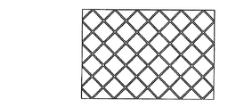
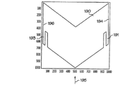
前記マイクロミラーアレイは4つの辺を有し、マイクロミラーの辺は何れもマイクロミラーアレイの辺とは平行でなく、
前記光源からの入射光は、前記マイクロミラーアレイの1つの辺に対して直角に入射し、
さらに、前記マイクロミラーの下には、当該マイクロミラーの回転軸を前記入射した光に対して垂直にするヒンジが、当該マイクロミラーと平行の間隔をおいた異なる平面上に形成されている、投射ディスプレイ。 - 前記マイクロミラーアレイの上方から見た場合に、マイクロミラーの辺は何れも入射光と平行でない請求項1に記載の投射ディスプレイ。
- マイクロミラーの回転軸は前記マイクロミラーアレイの1つの辺と平行である請求項1に記載の投射ディスプレイ。
- 前記マイクロミラーは正方形である請求項1に記載の投射ディスプレイ。
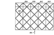
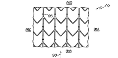
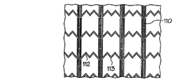
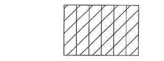
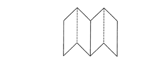
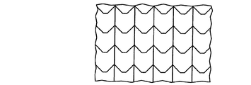
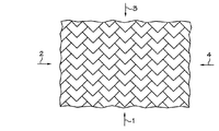
- 前記マイクロミラーはマイクロミラーアレイのX軸とY軸に対して平行でない角度をなす格子状に配列された請求項1に記載の投射ディスプレイ。
- 前記マイクロミラーは、前記ヒンジを介して基板に接続されたマイクロミラー板を有しており、
前記ヒンジとマイクロミラー板とによって第1の間隙が規定され、マイクロミラー板と基板との間に第2の間隙が規定される請求項1に記載の投射ディスプレイ。 - 隣接するマイクロミラーの間の間隙は0.1μm〜10μmである請求項1に記載の投射ディスプレイ。
- 前記隣接するマイクロミラーの間の間隙は0.7μmである請求項7に記載の投射ディスプレイ。
- 前記マイクロミラーアレイは、光を透過する窓を有するパッケージ内に設けられた請求項1に記載の投射ディスプレイ。
- 前記パッケージの一部にはマスクが設けられている請求項9に記載の投射ディスプレイ。
- 前記パッケージには分子スカベンジャーが設けられている請求項9に記載の投射ディスプレイ。
- 前記パッケージにはゲッターが設けられている請求項9に記載の投射ディスプレイ。
- 前記パッケージには、減スティクション剤が設けられている請求項9に記載の投射ディスプレイ。
- フロントスクリーンプロジェクションテレビである請求項1に記載の投射ディスプレイ。
- リアスクリーンプロジェクションテレビである請求項1に記載の投射ディスプレイ。
- コンピュータモニタである請求項1に記載の投射ディスプレイ。
- カラーホイールを備えた請求項1に記載の投射ディスプレイ。
- マイクロミラーアレイに照射される光は、マイクロミラーの平面に対する垂線に対して10から50度の角度を形成する請求項1に記載の投射ディスプレイ。
- 前記マイクロミラーは半導体基板上に設けられた請求項1に記載の投射ディスプレイ。
- 前記半導体基板はシリコン基板である請求項19に記載の投射ディスプレイ。
- 前記マイクロミラーが光透過性の基板上に設けられた請求項1に記載の投射ディスプレイ。
- 前記光透過性の基板はガラス製である請求項21に記載の投射ディスプレイ。
- 前記光透過性の基板はクォーツ又はサファイアである請求項21に記載の投射ディスプレイ。
- 前記光透過性の窓はガラス製である請求項9に記載の投射ディスプレイ。
- 前記光透過性の窓はクォーツである請求項9に記載の投射ディスプレイ。
- 前記光透過性の窓はポリマーである請求項9に記載の投射ディスプレイ。
- 前記マイクロミラーはON位置に向かって少なくとも+12度回転することができる請求項1に記載の投射ディスプレイ。
- 前記マイクロミラーのON位置は、傾斜の無い位置に対して10から15度傾斜している請求項1に記載の投射ディスプレイ。
- 前記マイクロミラーのONとOFF位置はマイクロミラーが当接する対象によって規定される請求項1に記載の投射ディスプレイ。
- さらにONとOFFのミラーパターンが入射するスクリーンを有する請求項1に記載の投射ディスプレイ。
- 前記マイクロミラーアレイのパターンをターゲットに投影するための複数のレンズを含む光学系を備えた請求項1に記載の投射ディスプレイ。
- さらにカラーホィールと、導光管とスクリーンを備えた請求項1に記載の投射ディスプレイ。
- マイクロミラーが回路と電極に隣接する基板上に形成され、少なくとも2つの電極がマイクロミラーの近傍に設けられ、1つの電極がOFF位置に当該隣接するマイクロミラーを静電的に引き寄せ、他の1つの電極がON位置に隣接するマイクロミラーを静電的に引き寄せる請求項1に記載の投射ディスプレイ。
- 前記回路と電極がマイクロミラーと同じ基板上に形成されている請求項1に記載の投射ディスプレイ。
- 前記隣接するマイクロミラーがONまたはOFF位置に到達したときに当該マイクロミラーを停止させる追加の電極を備えた請求項1に記載の投射ディスプレイ。
- 前記追加の電極は隣接するマイクロミラーと同じポテンシャルである請求項35に記載の投射ディスプレイ。
- 前記マイクロミラーは金属と誘電性材料を含む請求項1に記載の投射ディスプレイ。
- 前記誘電性材料はシリコンの窒素化合物、炭素化合物又は酸化物である請求項37に記載の投射ディスプレイ。
- 前記マイクロミラーアレイはパッケージ内に設けられ、回路と電極が半導体上に形成され、ボンドワイヤが基板とパッケージを接続する請求項1に記載の投射ディスプレイ。
- 前記マイクロミラーのヒンジは入射する光の方向に対して垂直に延びている請求項1に記載の投射ディスプレイ。
- 前記マイクロミラーのヒンジはマイクロミラーアレイの先頭辺と後尾辺とに対して平行に延びている請求項1に記載の投射ディスプレイ。
- 前記マイクロミラーアレイを上から見た場合、マイクロミラーアレイに入射する光を規定する直線がマイクロミラーのいずれの辺とも平行でない請求項1に記載の投射ディスプレイ。
- 前記マイクロミラーはL型である請求項1に記載の投射ディスプレイ。
- 前記マイクロミラーはひし形である請求項1に記載の投射ディスプレイ。
- 前記マイクロミラーは相互に実質的に隙間無く設けられている請求項1に記載の投射ディスプレイ。
- 前記4つの辺を有するマイクロミラーアレイは長方形で、光源からの光線は当該アレイの最も近い辺から垂直に立てた直線に対してプラスマイナス40度の範囲から入射する請求項1に記載の投射ディスプレイ。
- 前記マイクロミラーは金又はチタニウムのいずれかからなる反射材を有する請求項1に記載の投射ディスプレイ。
- 前記マイクロミラーはアルミニウムを含有する反射材を有する請求項1に記載の投射ディスプレイ。
- 前記マイクロミラーは銀を含有する反射材を有する請求項1に記載の投射ディスプレイ。
- 前記マイクロミラーのOFF状態での角度は、ON状態における逆方向の角度よりも小さい請求項1に記載の投射ディスプレイ。
- 各マイクロミラーの回転軸はマイクロミラーアレイの1つの辺に実質的に平行である請求項1に記載の投射ディスプレイ。
- 各マイクロミラーの回転軸はマイクロミラーの1つ以上の側面に対して35〜60度の範囲である請求項51に記載の投射ディスプレイ。
- 前記入射光はマイクロミラーのいずれの辺に対しても垂直でない請求項1に記載の投射ディスプレイ。
- 前記ヒンジの幅は0.1から10μmの間である請求項1に記載の投射ディスプレイ。
- マイクロミラーは光が入射する側の先頭側に、角張った突出部を有する請求項1に記載の投射ディスプレイ。
- 前記マイクロミラーは、当該マイクロミラーを動かすための電極および回路が形成された基板と同一の基板上に設けてある、請求項1に記載の投射ディスプレイ。
- 各マイクロミラーが非撓み位置からオン位置およびオフ位置に変位可能なように、前記マイクロミラーアレイは、基板上に支持されている請求項1に記載の投射ディスプレイ。
- 前記ヒンジは、導電層から形成されている請求項1に記載の投射ディスプレイ。
- 前記導電性材料はアルミニウム、合金又は導電性セラミック組成物のいずれかである請求項58に記載の投射ディスプレイ。
- 各マイクロミラーはマイクロミラーを1つの方向に変位させる第1の電極と、マイクロミラーを第2の方向に変位させる第2の電極と、マイクロミラーを停止させる第3の電極とを有する請求項1に記載の投射ディスプレイ。
- さらにマイクロミラー相互間の間隙によって散乱する光を低減するためにマイクロミラーの下に光を吸収する層を有する請求項1に記載の投射ディスプレイ。
- 64000〜2000000個のマイクロミラーを有する請求項1に記載の投射ディスプレイ。
- さらにTIRプリズムを有する請求項1に記載の投射ディスプレイ。
- さらに導光管を有する請求項1に記載の投射ディスプレイ。
- マイクロミラーアレイは1920000〜3145728個のマイクロミラーを有する請求項1に記載の投射ディスプレイ。
- マイクロミラーの辺は当該ミラーの面に対して入射する光の軸に対して80度未満の角度をなしている請求項1に記載の投射ディスプレイ。
- マイクロミラーの辺は当該ミラーの面に対して入射する光の軸に対して55度以下の角度をなしている請求項66に記載の投射ディスプレイ。
- マイクロミラーの辺は当該ミラーの面に対して入射する光の軸に対して45度以下の角度をなしている請求項67に記載の投射ディスプレイ。
- マイクロミラーの辺は当該ミラーの面に対して入射する光の軸に対して40度以下の角度をなしている請求項67に記載の投射ディスプレイ。
- 1平方cm以上1平方インチの面積に、3000000個以上のマイクロミラーが存在する請求項1に記載の投射ディスプレイ。
- 前記マイクロミラーは1920000以上の解像度を有する請求項1に記載の投射ディスプレイ。
- HDTVフォーマットを有する請求項1に記載の投射ディスプレイ。
- QXGAフォーマットを有する請求項1に記載の投射ディスプレイ。
- UXGAフォーマットを有する請求項1に記載の投射ディスプレイ。
- 前記マイクロミラーは凸な多角形状である請求項1に記載の投射ディスプレイ。
- 前記マイクロミラーは2つの多角形からなる辺を有し、それらがなす各は90度より小さい請求項1に記載の投射ディスプレイ。
- マイクロミラーアレイに光を供給する光源と、
複数のマイクロミラーの辺によって規定される形状を有するマイクロミラーからなるマイクロミラーアレイと、
を備え、
作動中は前記光源からの光がマイクロミラーアレイに入射し、
前記マイクロミラーアレイは4つの辺を有し、マイクロミラーの辺は何れもマイクロミラーアレイのどの辺とも平行ではなく、
マイクロミラーはOFF状態とON状態との間を動くことができ、マイクロミラーは画像のピクセルに対応するものであり、
前記光源からの入射光は、前記マイクロミラーアレイの1つの辺に対して直角に入射し、
さらに、前記マイクロミラーの下には、当該マイクロミラーの回転軸を前記入射した光に対して垂直にするヒンジが、当該マイクロミラーと平行の間隔をおいた異なる平面上に形成されている、投射ディスプレイ。 - さらにカラーホイールを有する請求項77に記載の投射ディスプレイ。
- 前記アレイを上から見たときに、マイクロミラーの辺は何れも入射する光と平行ではない請求項77に記載の投射ディスプレイ。
- 前記マイクロミラーはアレイのX、Y軸に対して傾斜した格子状に配置されている請求項77に記載の投射ディスプレイ。
- 前記マイクロミラーが実質的に隙間無く設けられた請求項77に記載の投射ディスプレイ。
Applications Claiming Priority (3)
| Application Number | Priority Date | Filing Date | Title |
|---|---|---|---|
| US09/631,536 US6529310B1 (en) | 1998-09-24 | 2000-08-03 | Deflectable spatial light modulator having superimposed hinge and deflectable element |
| US22924600P | 2000-08-30 | 2000-08-30 | |
| US09/732,445 US6523961B2 (en) | 2000-08-30 | 2000-12-07 | Projection system and mirror elements for improved contrast ratio in spatial light modulators |
Related Parent Applications (1)
| Application Number | Title | Priority Date | Filing Date |
|---|---|---|---|
| JP2002517555A Division JP3889705B2 (ja) | 2000-08-03 | 2001-08-03 | マイクロミラー素子、マイクロミラー素子用のパッケージ、およびそのための投射システム |
Publications (2)
| Publication Number | Publication Date |
|---|---|
| JP2005099793A JP2005099793A (ja) | 2005-04-14 |
| JP3889757B2 true JP3889757B2 (ja) | 2007-03-07 |
Family
ID=27397927
Family Applications (5)
| Application Number | Title | Priority Date | Filing Date |
|---|---|---|---|
| JP2002517555A Expired - Fee Related JP3889705B2 (ja) | 2000-08-03 | 2001-08-03 | マイクロミラー素子、マイクロミラー素子用のパッケージ、およびそのための投射システム |
| JP2004257715A Expired - Fee Related JP3889757B2 (ja) | 2000-08-03 | 2004-09-03 | マイクロミラー素子、マイクロミラー素子用のパッケージ、およびそのための投射システム |
| JP2004272332A Expired - Fee Related JP3768514B2 (ja) | 2000-08-03 | 2004-09-17 | マイクロミラー素子、マイクロミラー素子用のパッケージ、およびそのための投射システム |
| JP2004272333A Expired - Fee Related JP3889759B2 (ja) | 2000-08-03 | 2004-09-17 | マイクロミラー素子、マイクロミラー素子用のパッケージ、およびそのための投射システム |
| JP2005353848A Abandoned JP2006178447A (ja) | 2000-08-03 | 2005-12-07 | マイクロミラー素子、マイクロミラー素子用のパッケージ、およびそのための投射システム |
Family Applications Before (1)
| Application Number | Title | Priority Date | Filing Date |
|---|---|---|---|
| JP2002517555A Expired - Fee Related JP3889705B2 (ja) | 2000-08-03 | 2001-08-03 | マイクロミラー素子、マイクロミラー素子用のパッケージ、およびそのための投射システム |
Family Applications After (3)
| Application Number | Title | Priority Date | Filing Date |
|---|---|---|---|
| JP2004272332A Expired - Fee Related JP3768514B2 (ja) | 2000-08-03 | 2004-09-17 | マイクロミラー素子、マイクロミラー素子用のパッケージ、およびそのための投射システム |
| JP2004272333A Expired - Fee Related JP3889759B2 (ja) | 2000-08-03 | 2004-09-17 | マイクロミラー素子、マイクロミラー素子用のパッケージ、およびそのための投射システム |
| JP2005353848A Abandoned JP2006178447A (ja) | 2000-08-03 | 2005-12-07 | マイクロミラー素子、マイクロミラー素子用のパッケージ、およびそのための投射システム |
Country Status (8)
| Country | Link |
|---|---|
| EP (1) | EP1315993A4 (ja) |
| JP (5) | JP3889705B2 (ja) |
| KR (1) | KR100724081B1 (ja) |
| CN (5) | CN100412604C (ja) |
| AT (1) | ATE354814T1 (ja) |
| AU (1) | AU2001281019A1 (ja) |
| DE (10) | DE20122372U1 (ja) |
| WO (1) | WO2002012925A2 (ja) |
Families Citing this family (51)
| Publication number | Priority date | Publication date | Assignee | Title |
|---|---|---|---|---|
| US6969635B2 (en) | 2000-12-07 | 2005-11-29 | Reflectivity, Inc. | Methods for depositing, releasing and packaging micro-electromechanical devices on wafer substrates |
| US7018052B2 (en) | 2000-08-30 | 2006-03-28 | Reflectivity, Inc | Projection TV with improved micromirror array |
| US7307775B2 (en) * | 2000-12-07 | 2007-12-11 | Texas Instruments Incorporated | Methods for depositing, releasing and packaging micro-electromechanical devices on wafer substrates |
| US7023606B2 (en) | 2001-08-03 | 2006-04-04 | Reflectivity, Inc | Micromirror array for projection TV |
| SG111972A1 (en) * | 2002-10-17 | 2005-06-29 | Agency Science Tech & Res | Wafer-level package for micro-electro-mechanical systems |
| US7042622B2 (en) | 2003-10-30 | 2006-05-09 | Reflectivity, Inc | Micromirror and post arrangements on substrates |
| US7397517B2 (en) * | 2003-05-30 | 2008-07-08 | Kazuhiro Ohara | Display system and signal processing using diamond-shaped DMDs |
| US6871958B2 (en) | 2003-08-18 | 2005-03-29 | Evans & Sutherland Computer Corporation | Wide angle scanner for panoramic display |
| US7012669B2 (en) | 2003-08-18 | 2006-03-14 | Evans & Sutherland Computer Corporation | Reflection barrier for panoramic display |
| US7334902B2 (en) | 2003-08-18 | 2008-02-26 | Evans & Sutherland Computer Corporation | Wide angle scanner for panoramic display |
| US6861277B1 (en) * | 2003-10-02 | 2005-03-01 | Hewlett-Packard Development Company, L.P. | Method of forming MEMS device |
| US6995830B2 (en) * | 2003-12-22 | 2006-02-07 | Asml Netherlands B.V. | Lithographic projection apparatus and device manufacturing method |
| US7057794B2 (en) * | 2004-05-19 | 2006-06-06 | Taiwan Semiconductor Manufacturing Company, Ltd. | Micromirror for MEMS device |
| US7273693B2 (en) * | 2004-07-30 | 2007-09-25 | Hewlett-Packard Development Company, L.P. | Method for forming a planar mirror using a sacrificial oxide |
| US7038831B2 (en) * | 2004-09-30 | 2006-05-02 | Lucent Technologies, Inc. | Micromirror apparatus with improved in-plane rotation tolerance |
| KR100815358B1 (ko) * | 2004-10-08 | 2008-03-19 | 삼성전기주식회사 | 경사진 광투과성 덮개를 가진 광변조기 패키지 |
| JP4568579B2 (ja) | 2004-10-29 | 2010-10-27 | 富士通株式会社 | 光スイッチ |
| IL165212A (en) | 2004-11-15 | 2012-05-31 | Elbit Systems Electro Optics Elop Ltd | Device for scanning light |
| US7372617B2 (en) * | 2005-07-06 | 2008-05-13 | Peter Enoksson | Hidden hinge MEMS device |
| GB2453104B (en) * | 2007-09-19 | 2012-04-25 | Wolfson Microelectronics Plc | Mems device and process |
| US11157977B1 (en) | 2007-10-26 | 2021-10-26 | Zazzle Inc. | Sales system using apparel modeling system and method |
| TWI418850B (zh) * | 2007-11-09 | 2013-12-11 | 尼康股份有限公司 | 微致動器、光學設備、顯示裝置、曝光裝置及設備製造方法 |
| JP2009233836A (ja) * | 2008-03-28 | 2009-10-15 | Yamaha Corp | Memsおよびmems製造方法 |
| WO2009126263A1 (en) * | 2008-04-08 | 2009-10-15 | Cornell University | Multi-axis, large tilt angle, wafer level micromirror array for large scale beam steering applications |
| DE102008001038B4 (de) | 2008-04-08 | 2016-08-11 | Robert Bosch Gmbh | Mikromechanisches Bauelement mit Schrägstruktur und entsprechendes Herstellungsverfahren |
| US8096182B2 (en) * | 2008-05-29 | 2012-01-17 | Freescale Semiconductor, Inc. | Capacitive sensor with stress relief that compensates for package stress |
| JP5151756B2 (ja) * | 2008-07-16 | 2013-02-27 | 株式会社豊田中央研究所 | 光学装置 |
| US10719862B2 (en) | 2008-07-29 | 2020-07-21 | Zazzle Inc. | System and method for intake of manufacturing patterns and applying them to the automated production of interactive, customizable product |
| WO2011006522A1 (en) * | 2009-07-17 | 2011-01-20 | Carl Zeiss Smt Gmbh | Microlithographic projection exposure apparatus and method of measuring a parameter related to an optical surface contained therein |
| KR101912092B1 (ko) | 2010-10-05 | 2018-10-26 | 삼성전자 주식회사 | 액체 렌즈 |
| KR101912093B1 (ko) | 2010-10-29 | 2018-10-26 | 삼성전자 주식회사 | 광학 장치 |
| CN102087414B (zh) * | 2010-11-03 | 2012-12-26 | 凝辉(天津)科技有限责任公司 | 一种阵列式分区投影方法 |
| CN102683474B (zh) * | 2011-03-18 | 2014-11-05 | 浙江大立科技股份有限公司 | 一种基于复合牺牲层的红外探测器制作方法 |
| US9641826B1 (en) | 2011-10-06 | 2017-05-02 | Evans & Sutherland Computer Corporation | System and method for displaying distant 3-D stereo on a dome surface |
| US10969743B2 (en) | 2011-12-29 | 2021-04-06 | Zazzle Inc. | System and method for the efficient recording of large aperture wave fronts of visible and near visible light |
| AU2013294616B2 (en) | 2012-07-26 | 2016-04-28 | Apple Inc. | Dual-axis scanning mirror |
| US9110354B2 (en) * | 2012-09-20 | 2015-08-18 | Palo Alto Research Center Incorporated | Steerable illumination source for a compact camera |
| US9482863B2 (en) | 2012-10-23 | 2016-11-01 | Apple Inc. | Production of micro-mechanical devices |
| DE102013213842A1 (de) * | 2013-07-16 | 2015-01-22 | Carl Zeiss Smt Gmbh | Optisches Bauelement |
| DE102013217269A1 (de) * | 2013-08-29 | 2015-03-05 | Carl Zeiss Smt Gmbh | Mikrospiegel-Array |
| CN103777450A (zh) * | 2014-01-06 | 2014-05-07 | 吴震 | 发光装置、投影显示装置和发光系统 |
| CN103777445B (zh) * | 2014-01-06 | 2018-12-25 | 杨毅 | 投影显示装置 |
| JP2016029430A (ja) * | 2014-07-25 | 2016-03-03 | セイコーエプソン株式会社 | 電気光学装置、電気光学装置の製造方法、及び電子機器 |
| DE102015200626B3 (de) | 2015-01-16 | 2016-07-21 | Fraunhofer-Gesellschaft zur Förderung der angewandten Forschung e.V. | MEMS Aktuator, System mit einer Mehrzahl vom MEMS Aktuatoren und Verfahren zum Herstellen eines MEMS Aktuators |
| CN104835908A (zh) * | 2015-04-17 | 2015-08-12 | 上海华虹宏力半导体制造有限公司 | 用于3d amr的氮化钽刻蚀方法 |
| US10589980B2 (en) * | 2017-04-07 | 2020-03-17 | Texas Instruments Incorporated | Isolated protrusion/recession features in a micro electro mechanical system |
| DE102018207783B4 (de) | 2018-05-17 | 2022-11-10 | Fraunhofer-Gesellschaft zur Förderung der angewandten Forschung e.V. | MEMS-Array aus MEMS mit jeweils einem beweglichen Strukturelement |
| CN111246187B (zh) * | 2018-11-29 | 2022-07-29 | 青岛海信激光显示股份有限公司 | 光阀驱动控制方法及投影设备 |
| KR102211618B1 (ko) * | 2019-07-26 | 2021-02-02 | 인하대학교 산학협력단 | 3차원 플로팅 이미지 구현 장치용 역반사 마이크로 미러 어레이 |
| CN113675722B (zh) * | 2021-07-14 | 2024-10-29 | 威科赛乐微电子股份有限公司 | 一种Cap layer层蚀刻优化方法 |
| WO2025127562A1 (ko) * | 2023-12-14 | 2025-06-19 | 엘지이노텍 주식회사 | 프로젝트 장치 및 이를 포함하는 전자 디바이스 |
Family Cites Families (12)
| Publication number | Priority date | Publication date | Assignee | Title |
|---|---|---|---|---|
| US4592628A (en) * | 1981-07-01 | 1986-06-03 | International Business Machines | Mirror array light valve |
| US5659374A (en) * | 1992-10-23 | 1997-08-19 | Texas Instruments Incorporated | Method of repairing defective pixels |
| US5696619A (en) * | 1995-02-27 | 1997-12-09 | Texas Instruments Incorporated | Micromechanical device having an improved beam |
| JPH08304924A (ja) * | 1995-05-10 | 1996-11-22 | Nikon Corp | プロジェクター装置 |
| JPH08304892A (ja) * | 1995-05-11 | 1996-11-22 | Asahi Optical Co Ltd | ストロボ付カメラ |
| US6288828B1 (en) * | 1997-09-10 | 2001-09-11 | Light And Sound Design Ltd. | Programmable light beam shape altering device using programmable micromirrors |
| KR100243190B1 (ko) * | 1996-06-10 | 2000-02-01 | 윤종용 | 가동미러장치 및 그 제조방법 |
| EP0877272B1 (en) * | 1997-05-08 | 2002-07-31 | Texas Instruments Incorporated | Improvements in or relating to spatial light modulators |
| KR100313851B1 (ko) * | 1998-04-10 | 2001-12-12 | 윤종용 | 화상표시장치용마이크로미러디바이스 |
| US6123985A (en) * | 1998-10-28 | 2000-09-26 | Solus Micro Technologies, Inc. | Method of fabricating a membrane-actuated charge controlled mirror (CCM) |
| US6222667B1 (en) * | 1999-02-09 | 2001-04-24 | Advanced Optics Electronics, Inc. | Electro-optic light valve array |
| US6175443B1 (en) * | 1999-05-01 | 2001-01-16 | Lucent Technologies, Inc. | Article comprising a deformable segmented mirror |
-
2001
- 2001-08-03 WO PCT/US2001/024332 patent/WO2002012925A2/en not_active Ceased
- 2001-08-03 AT AT05000599T patent/ATE354814T1/de not_active IP Right Cessation
- 2001-08-03 DE DE20122372U patent/DE20122372U1/de not_active Expired - Lifetime
- 2001-08-03 DE DE60126849T patent/DE60126849T2/de not_active Expired - Fee Related
- 2001-08-03 CN CNB2004100546604A patent/CN100412604C/zh not_active Expired - Fee Related
- 2001-08-03 DE DE20122373U patent/DE20122373U1/de not_active Expired - Lifetime
- 2001-08-03 DE DE20122618U patent/DE20122618U1/de not_active Expired - Lifetime
- 2001-08-03 CN CNB2004100546572A patent/CN100412602C/zh not_active Expired - Fee Related
- 2001-08-03 EP EP01959466A patent/EP1315993A4/en not_active Ceased
- 2001-08-03 CN CNB018136087A patent/CN100392467C/zh not_active Expired - Fee Related
- 2001-08-03 DE DE20122371U patent/DE20122371U1/de not_active Expired - Lifetime
- 2001-08-03 DE DE20122616U patent/DE20122616U1/de not_active Expired - Lifetime
- 2001-08-03 AU AU2001281019A patent/AU2001281019A1/en not_active Abandoned
- 2001-08-03 DE DE20122370U patent/DE20122370U1/de not_active Expired - Lifetime
- 2001-08-03 CN CNB2004100546587A patent/CN100412603C/zh not_active Expired - Fee Related
- 2001-08-03 DE DE20122615U patent/DE20122615U1/de not_active Expired - Lifetime
- 2001-08-03 DE DE20122617U patent/DE20122617U1/de not_active Expired - Lifetime
- 2001-08-03 JP JP2002517555A patent/JP3889705B2/ja not_active Expired - Fee Related
- 2001-08-03 DE DE20122614U patent/DE20122614U1/de not_active Expired - Lifetime
- 2001-08-03 CN CNB2004100546591A patent/CN100371763C/zh not_active Expired - Fee Related
-
2003
- 2003-02-03 KR KR1020037001542A patent/KR100724081B1/ko not_active Expired - Fee Related
-
2004
- 2004-09-03 JP JP2004257715A patent/JP3889757B2/ja not_active Expired - Fee Related
- 2004-09-17 JP JP2004272332A patent/JP3768514B2/ja not_active Expired - Fee Related
- 2004-09-17 JP JP2004272333A patent/JP3889759B2/ja not_active Expired - Fee Related
-
2005
- 2005-12-07 JP JP2005353848A patent/JP2006178447A/ja not_active Abandoned
Also Published As
Similar Documents
| Publication | Publication Date | Title |
|---|---|---|
| JP3889757B2 (ja) | マイクロミラー素子、マイクロミラー素子用のパッケージ、およびそのための投射システム | |
| US7006275B2 (en) | Packaged micromirror array for a projection display | |
| US7023606B2 (en) | Micromirror array for projection TV | |
| US6962419B2 (en) | Micromirror elements, package for the micromirror elements, and projection system therefor | |
| JP2005115370A (ja) | Memsデバイスおよびmemsデバイスの形成方法 | |
| CN1748168A (zh) | 用于投影显示器中微型反射镜阵列的微型反射镜和偏离对角线的铰链结构 | |
| US7151628B2 (en) | Micromirror array device and a method for making the same | |
| EP1553437B1 (en) | Singulated wafer die having micromirrors |
Legal Events
| Date | Code | Title | Description |
|---|---|---|---|
| A621 | Written request for application examination |
Free format text: JAPANESE INTERMEDIATE CODE: A621 Effective date: 20040903 |
|
| A871 | Explanation of circumstances concerning accelerated examination |
Free format text: JAPANESE INTERMEDIATE CODE: A871 Effective date: 20040903 |
|
| A975 | Report on accelerated examination |
Free format text: JAPANESE INTERMEDIATE CODE: A971005 Effective date: 20050210 |
|
| A131 | Notification of reasons for refusal |
Free format text: JAPANESE INTERMEDIATE CODE: A131 Effective date: 20050322 |
|
| RD02 | Notification of acceptance of power of attorney |
Free format text: JAPANESE INTERMEDIATE CODE: A7422 Effective date: 20050318 |
|
| RD04 | Notification of resignation of power of attorney |
Free format text: JAPANESE INTERMEDIATE CODE: A7424 Effective date: 20050425 |
|
| RD04 | Notification of resignation of power of attorney |
Free format text: JAPANESE INTERMEDIATE CODE: A7424 Effective date: 20050425 |
|
| A601 | Written request for extension of time |
Free format text: JAPANESE INTERMEDIATE CODE: A601 Effective date: 20050616 |
|
| A602 | Written permission of extension of time |
Free format text: JAPANESE INTERMEDIATE CODE: A602 Effective date: 20050621 |
|
| A521 | Request for written amendment filed |
Free format text: JAPANESE INTERMEDIATE CODE: A523 Effective date: 20050922 |
|
| A131 | Notification of reasons for refusal |
Free format text: JAPANESE INTERMEDIATE CODE: A131 Effective date: 20060131 |
|
| A601 | Written request for extension of time |
Free format text: JAPANESE INTERMEDIATE CODE: A601 Effective date: 20060428 |
|
| A602 | Written permission of extension of time |
Free format text: JAPANESE INTERMEDIATE CODE: A602 Effective date: 20060509 |
|
| A521 | Request for written amendment filed |
Free format text: JAPANESE INTERMEDIATE CODE: A523 Effective date: 20060519 |
|
| A524 | Written submission of copy of amendment under article 19 pct |
Free format text: JAPANESE INTERMEDIATE CODE: A524 Effective date: 20060519 |
|
| A521 | Request for written amendment filed |
Free format text: JAPANESE INTERMEDIATE CODE: A523 Effective date: 20060601 |
|
| A072 | Dismissal of procedure [no reply to invitation to correct request for examination] |
Free format text: JAPANESE INTERMEDIATE CODE: A072 Effective date: 20061027 |
|
| TRDD | Decision of grant or rejection written | ||
| A01 | Written decision to grant a patent or to grant a registration (utility model) |
Free format text: JAPANESE INTERMEDIATE CODE: A01 Effective date: 20061113 |
|
| A61 | First payment of annual fees (during grant procedure) |
Free format text: JAPANESE INTERMEDIATE CODE: A61 Effective date: 20061130 |
|
| R150 | Certificate of patent or registration of utility model |
Free format text: JAPANESE INTERMEDIATE CODE: R150 |
|
| LAPS | Cancellation because of no payment of annual fees |