JP3869849B2 - Manufacturing method of semiconductor device - Google Patents
Manufacturing method of semiconductor device Download PDFInfo
- Publication number
- JP3869849B2 JP3869849B2 JP2006072498A JP2006072498A JP3869849B2 JP 3869849 B2 JP3869849 B2 JP 3869849B2 JP 2006072498 A JP2006072498 A JP 2006072498A JP 2006072498 A JP2006072498 A JP 2006072498A JP 3869849 B2 JP3869849 B2 JP 3869849B2
- Authority
- JP
- Japan
- Prior art keywords
- metal layer
- semiconductor device
- metal
- semiconductor element
- resin
- Prior art date
- Legal status (The legal status is an assumption and is not a legal conclusion. Google has not performed a legal analysis and makes no representation as to the accuracy of the status listed.)
- Expired - Lifetime
Links
Images


Classifications
-
- H—ELECTRICITY
- H01—ELECTRIC ELEMENTS
- H01L—SEMICONDUCTOR DEVICES NOT COVERED BY CLASS H10
- H01L24/00—Arrangements for connecting or disconnecting semiconductor or solid-state bodies; Methods or apparatus related thereto
- H01L24/93—Batch processes
- H01L24/95—Batch processes at chip-level, i.e. with connecting carried out on a plurality of singulated devices, i.e. on diced chips
- H01L24/97—Batch processes at chip-level, i.e. with connecting carried out on a plurality of singulated devices, i.e. on diced chips the devices being connected to a common substrate, e.g. interposer, said common substrate being separable into individual assemblies after connecting
-
- H—ELECTRICITY
- H01—ELECTRIC ELEMENTS
- H01L—SEMICONDUCTOR DEVICES NOT COVERED BY CLASS H10
- H01L2224/00—Indexing scheme for arrangements for connecting or disconnecting semiconductor or solid-state bodies and methods related thereto as covered by H01L24/00
- H01L2224/01—Means for bonding being attached to, or being formed on, the surface to be connected, e.g. chip-to-package, die-attach, "first-level" interconnects; Manufacturing methods related thereto
- H01L2224/02—Bonding areas; Manufacturing methods related thereto
- H01L2224/04—Structure, shape, material or disposition of the bonding areas prior to the connecting process
- H01L2224/05—Structure, shape, material or disposition of the bonding areas prior to the connecting process of an individual bonding area
- H01L2224/0554—External layer
- H01L2224/0555—Shape
- H01L2224/05552—Shape in top view
- H01L2224/05553—Shape in top view being rectangular
-
- H—ELECTRICITY
- H01—ELECTRIC ELEMENTS
- H01L—SEMICONDUCTOR DEVICES NOT COVERED BY CLASS H10
- H01L2224/00—Indexing scheme for arrangements for connecting or disconnecting semiconductor or solid-state bodies and methods related thereto as covered by H01L24/00
- H01L2224/01—Means for bonding being attached to, or being formed on, the surface to be connected, e.g. chip-to-package, die-attach, "first-level" interconnects; Manufacturing methods related thereto
- H01L2224/02—Bonding areas; Manufacturing methods related thereto
- H01L2224/04—Structure, shape, material or disposition of the bonding areas prior to the connecting process
- H01L2224/05—Structure, shape, material or disposition of the bonding areas prior to the connecting process of an individual bonding area
- H01L2224/0554—External layer
- H01L2224/0555—Shape
- H01L2224/05552—Shape in top view
- H01L2224/05554—Shape in top view being square
-
- H—ELECTRICITY
- H01—ELECTRIC ELEMENTS
- H01L—SEMICONDUCTOR DEVICES NOT COVERED BY CLASS H10
- H01L2224/00—Indexing scheme for arrangements for connecting or disconnecting semiconductor or solid-state bodies and methods related thereto as covered by H01L24/00
- H01L2224/01—Means for bonding being attached to, or being formed on, the surface to be connected, e.g. chip-to-package, die-attach, "first-level" interconnects; Manufacturing methods related thereto
- H01L2224/42—Wire connectors; Manufacturing methods related thereto
- H01L2224/44—Structure, shape, material or disposition of the wire connectors prior to the connecting process
- H01L2224/45—Structure, shape, material or disposition of the wire connectors prior to the connecting process of an individual wire connector
- H01L2224/45001—Core members of the connector
- H01L2224/45099—Material
- H01L2224/451—Material with a principal constituent of the material being a metal or a metalloid, e.g. boron (B), silicon (Si), germanium (Ge), arsenic (As), antimony (Sb), tellurium (Te) and polonium (Po), and alloys thereof
- H01L2224/45138—Material with a principal constituent of the material being a metal or a metalloid, e.g. boron (B), silicon (Si), germanium (Ge), arsenic (As), antimony (Sb), tellurium (Te) and polonium (Po), and alloys thereof the principal constituent melting at a temperature of greater than or equal to 950°C and less than 1550°C
- H01L2224/45144—Gold (Au) as principal constituent
-
- H—ELECTRICITY
- H01—ELECTRIC ELEMENTS
- H01L—SEMICONDUCTOR DEVICES NOT COVERED BY CLASS H10
- H01L2224/00—Indexing scheme for arrangements for connecting or disconnecting semiconductor or solid-state bodies and methods related thereto as covered by H01L24/00
- H01L2224/01—Means for bonding being attached to, or being formed on, the surface to be connected, e.g. chip-to-package, die-attach, "first-level" interconnects; Manufacturing methods related thereto
- H01L2224/42—Wire connectors; Manufacturing methods related thereto
- H01L2224/47—Structure, shape, material or disposition of the wire connectors after the connecting process
- H01L2224/48—Structure, shape, material or disposition of the wire connectors after the connecting process of an individual wire connector
- H01L2224/481—Disposition
- H01L2224/48151—Connecting between a semiconductor or solid-state body and an item not being a semiconductor or solid-state body, e.g. chip-to-substrate, chip-to-passive
- H01L2224/48221—Connecting between a semiconductor or solid-state body and an item not being a semiconductor or solid-state body, e.g. chip-to-substrate, chip-to-passive the body and the item being stacked
- H01L2224/48245—Connecting between a semiconductor or solid-state body and an item not being a semiconductor or solid-state body, e.g. chip-to-substrate, chip-to-passive the body and the item being stacked the item being metallic
- H01L2224/48247—Connecting between a semiconductor or solid-state body and an item not being a semiconductor or solid-state body, e.g. chip-to-substrate, chip-to-passive the body and the item being stacked the item being metallic connecting the wire to a bond pad of the item
-
- H—ELECTRICITY
- H01—ELECTRIC ELEMENTS
- H01L—SEMICONDUCTOR DEVICES NOT COVERED BY CLASS H10
- H01L2224/00—Indexing scheme for arrangements for connecting or disconnecting semiconductor or solid-state bodies and methods related thereto as covered by H01L24/00
- H01L2224/01—Means for bonding being attached to, or being formed on, the surface to be connected, e.g. chip-to-package, die-attach, "first-level" interconnects; Manufacturing methods related thereto
- H01L2224/42—Wire connectors; Manufacturing methods related thereto
- H01L2224/47—Structure, shape, material or disposition of the wire connectors after the connecting process
- H01L2224/49—Structure, shape, material or disposition of the wire connectors after the connecting process of a plurality of wire connectors
- H01L2224/491—Disposition
- H01L2224/4912—Layout
- H01L2224/49175—Parallel arrangements
-
- H—ELECTRICITY
- H01—ELECTRIC ELEMENTS
- H01L—SEMICONDUCTOR DEVICES NOT COVERED BY CLASS H10
- H01L2224/00—Indexing scheme for arrangements for connecting or disconnecting semiconductor or solid-state bodies and methods related thereto as covered by H01L24/00
- H01L2224/73—Means for bonding being of different types provided for in two or more of groups H01L2224/10, H01L2224/18, H01L2224/26, H01L2224/34, H01L2224/42, H01L2224/50, H01L2224/63, H01L2224/71
- H01L2224/732—Location after the connecting process
- H01L2224/73251—Location after the connecting process on different surfaces
- H01L2224/73265—Layer and wire connectors
-
- H—ELECTRICITY
- H01—ELECTRIC ELEMENTS
- H01L—SEMICONDUCTOR DEVICES NOT COVERED BY CLASS H10
- H01L2224/00—Indexing scheme for arrangements for connecting or disconnecting semiconductor or solid-state bodies and methods related thereto as covered by H01L24/00
- H01L2224/91—Methods for connecting semiconductor or solid state bodies including different methods provided for in two or more of groups H01L2224/80 - H01L2224/90
- H01L2224/92—Specific sequence of method steps
- H01L2224/922—Connecting different surfaces of the semiconductor or solid-state body with connectors of different types
- H01L2224/9222—Sequential connecting processes
- H01L2224/92242—Sequential connecting processes the first connecting process involving a layer connector
- H01L2224/92247—Sequential connecting processes the first connecting process involving a layer connector the second connecting process involving a wire connector
-
- H—ELECTRICITY
- H01—ELECTRIC ELEMENTS
- H01L—SEMICONDUCTOR DEVICES NOT COVERED BY CLASS H10
- H01L2924/00—Indexing scheme for arrangements or methods for connecting or disconnecting semiconductor or solid-state bodies as covered by H01L24/00
- H01L2924/15—Details of package parts other than the semiconductor or other solid state devices to be connected
- H01L2924/151—Die mounting substrate
- H01L2924/156—Material
- H01L2924/15786—Material with a principal constituent of the material being a non metallic, non metalloid inorganic material
- H01L2924/15787—Ceramics, e.g. crystalline carbides, nitrides or oxides
-
- H—ELECTRICITY
- H01—ELECTRIC ELEMENTS
- H01L—SEMICONDUCTOR DEVICES NOT COVERED BY CLASS H10
- H01L2924/00—Indexing scheme for arrangements or methods for connecting or disconnecting semiconductor or solid-state bodies as covered by H01L24/00
- H01L2924/15—Details of package parts other than the semiconductor or other solid state devices to be connected
- H01L2924/181—Encapsulation
Description
本発明は、半導体装置、その製造方法及び電着フレームに関し、特にリードレス表面実装型の樹脂封止された半導体装置と、その製造方法、及び半導体素子搭載用の電着フレームに関するものである。 The present invention relates to a semiconductor device, a manufacturing method thereof, and an electrodeposition frame, and more particularly to a leadless surface mounting type resin-encapsulated semiconductor device, a manufacturing method thereof, and an electrodeposition frame for mounting a semiconductor element.
図8は、従来の半導体装置を示す断面図であり、この半導体装置は、樹脂封止したリードレス表面実装型の半導体装置である。同図において、ガラスエポキシ基板(又はセラミック基板)1の一面に金属層31 ,32が形成され、かつ金属層32に対応するガラスエポキシ基板1の裏面に電極金属層5aが形成され、金属層32と電極金属層5aとがスルーホール6で電気的に接続されている。ガラスエポキシ基板1の一面の金属層31には、半導体素子2が接着され、半導体素子2の電極パッド2aと金属層32とがワイヤ4で電気的に接続されている。ワイヤ4で配線がなされた半導体素子2は、エポキシ樹脂7で樹脂封止されている。
FIG. 8 is a cross-sectional view showing a conventional semiconductor device, which is a resin-sealed leadless surface-mount type semiconductor device. In the figure, the
従来のリードレス表面実装型の半導体装置では、図8に示したように、ガラスエポキシ基板1に多数のスルーホール6が形成され、ガラスエポキシ基板1上に金属層31が多数形成され、それぞれに半導体素子2が接着されてワイヤ4で電極パッド2aと金属層32との配線がなされている。この半導体装置の製造工程では、一枚のガラスエポキシ基板に数百個単位で半導体素子が搭載されてワイヤボンディングされて、樹脂封止されている。従って、この構造の半導体装置では、スルーホール6の個数が半導体素子2の個数の数倍の数となり、スルーホール形成のための製造工数を無視することができず、この種の半導体装置の製造原価が高騰する要因となっていた。
In conventional leadless surface mount type semiconductor device, as shown in FIG. 8, a large number of through
また、従来のリードレス表面実装型の半導体装置では、スルーホールが形成されており、隣接する半導体素子間の隙間にスルーホールを形成するには、半導体素子間の隙間にスルーホールを形成するための領域を用意しなければならないので、実質的に一枚のガラスエポキシ基板に搭載される半導体素子の個数は制限され、製造原価を高騰させる要因となっていた。 In addition, in a conventional leadless surface mount type semiconductor device, through holes are formed. In order to form a through hole in a gap between adjacent semiconductor elements, a through hole is formed in the gap between semiconductor elements. Therefore, the number of semiconductor elements mounted on one glass epoxy substrate is substantially limited, which causes a rise in manufacturing costs.
更に、従来のリードレス表面実装型の半導体装置では、ガラスエポキシ基板上に半導体素子が搭載されて樹脂封止されている。そのため、半導体素子の動作時に発生した熱を発散させることができずガラスエポキシ基板に蓄積され、熱の放熱性が悪いという欠点があった。 Furthermore, in a conventional leadless surface mount type semiconductor device, a semiconductor element is mounted on a glass epoxy substrate and sealed with resin. For this reason, heat generated during the operation of the semiconductor element cannot be dissipated and accumulated on the glass epoxy substrate, resulting in a disadvantage that heat dissipation is poor.
本発明は、上記のような課題に鑑みてなされたものであって、リードレス表面実装型の半導体装置であって、製造原価が安価であって、放熱性が良い半導体装置、その製造方法及び電着フレームを提供することを目的とするものである。 The present invention has been made in view of the above-described problems, and is a leadless surface-mount type semiconductor device having a low manufacturing cost and good heat dissipation, a manufacturing method thereof, and The object is to provide an electrodeposition frame.
本発明は、上記課題を達成したものであり、請求項1の発明は、金属層に接着された半導体素子と、該半導体素子上の電極パッドと外部導出用の金属層とを電気的に接続するワイヤと、該ワイヤで配線を行った該半導体素子を封止する樹脂パッケージとを具備し、該半導体素子が接着されている金属層裏面と前記外部導出用の金属層裏面とが該樹脂パッケージ底面と同一平面であることを特徴とする半導体装置である。
The present invention achieves the above-mentioned problems, and the invention of
請求項1の発明によれば、樹脂パッケージ内に封止されている半導体素子が樹脂パッケージから露出する金属膜に搭載され、その外部導出用の金属層の底面も樹脂パッケージ底面より露呈したリードレス構造の半導体装置であり、ガラスエポキシ基板やセラミック基板が使用されていないので、半導体装置の高さを低背とすることができるため半導体素子から発生する熱の放熱性がよい利点がある。これら金属層は、薄膜状の金属層であり、リードを用いた半導体装置と比較して、熱伝導性が良好なリードレス型の半導体装置である。また、この半導体装置は、高価な基板を使用する必要がないので、比較的安価な半導体装置とすることができる。しかも、半導体装置裏面の金属層と樹脂パッケージとが同一平面(面一)であり、この半導体装置を回路基板に実装した際の回路基板との密着性が良く、しかも半導体素子から発生する熱が回路基板を介して放散し易い。さらに外部導出用の金属層裏面には、必要に応じて、極めて薄い平坦な電極金属層を成膜してもよい According to the first aspect of the present invention, the semiconductor element sealed in the resin package is mounted on the metal film exposed from the resin package, and the bottom surface of the metal layer for external derivation is exposed from the bottom surface of the resin package. Since the semiconductor device has a structure and does not use a glass epoxy substrate or a ceramic substrate, the height of the semiconductor device can be reduced, so that there is an advantage of good heat dissipation of heat generated from the semiconductor element. These metal layers are thin metal layers and are leadless semiconductor devices having better thermal conductivity than semiconductor devices using leads. Further, since this semiconductor device does not need to use an expensive substrate, it can be a relatively inexpensive semiconductor device. In addition, the metal layer on the back surface of the semiconductor device and the resin package are flush with each other and have good adhesion to the circuit board when the semiconductor device is mounted on the circuit board, and the heat generated from the semiconductor element is Easy to dissipate through the circuit board. Furthermore, an extremely thin flat electrode metal layer may be formed on the back surface of the metal layer for external derivation, if necessary.
また、請求項2の発明は、半導体素子が接着される金属層が該半導体素子底面の面積より広い面積であることを特徴とする請求項1に記載の半導体装置である。
The invention according to
請求項2の発明によれば、半導体素子が接着される金属層が半導体素子の底面の面積より広い面積であるので、樹脂パッケージの表面から半導体素子との沿面距離を充分に設けることができ、半導体素子の耐湿特性を高めることができる。
According to the invention of
また、請求項3の発明は、半導体素子が接着される金属層の膜厚を厚くし、かつ前記金属層の面積が該半導体素子底面の面積より狭いことを特徴とする請求項1に記載の半導体装置である。
The invention of
請求項3の発明によれば、半導体素子が接着される金属層の膜厚を厚くすることで、樹脂パッケージの底面から半導体素子までの沿面距離を充分に形成して、半導体装置としての耐湿性を高めることができるとともに、比較的サイズの大きな半導体素子を樹脂封止することができる。さらにまた、金属層の膜厚を厚くすることで、半導体素子を樹脂パッケージ内中央に配置させることができる。従って、半導体装置に熱ストレスが加わったとしても樹脂パッケージにひび割れが発生し難い。
According to the invention of
また、請求項4の発明は、樹脂パッケージ底面に前記外部導出用の金属層が独立して存在することを特徴とする請求項1,2又は3に記載の半導体装置である。 According to a fourth aspect of the present invention, there is provided the semiconductor device according to the first, second, or third aspect, wherein the externally leading metal layer is independently present on the bottom surface of the resin package.
請求項4の発明によれば、外部導出用の金属層の露呈面の形状を独立した不定形な任意の形状とすることができる。無論、金属層を連続するように形成することができる。
According to invention of
また、請求項5の発明は、可撓性平板状の金属基板に、パターニングされた金属層を形成した電着フレームを形成する工程と、前記電着フレームがパターニングされた前記金属層に複数の半導体素子を隣接して搭載する工程と、前記パターニングされた金属層に搭載される各半導体素子間に形成された外部導出用の金属層に、前記隣接する各半導体素子の電極パッドをワイヤで所定間隔を設けて電気的に共通接続するワイヤボンディング工程と、前記電着フレームに搭載されて配線がなされた半導体素子を樹脂封止する樹脂封止工程と、前記金属基板を剥離して樹脂封止体を得る剥離工程と、前記半導体素子が複数封止された樹脂封止体を、パターニングされた金属層の切断マークで個々の半導体装置に切断する切り出し工程と、を含むことを特徴とする半導体装置の製造方法である。 According to a fifth aspect of the present invention, there is provided a step of forming an electrodeposition frame in which a patterned metal layer is formed on a flexible flat metal substrate, and a plurality of the metal layers in which the electrodeposition frame is patterned. A step of mounting the semiconductor elements adjacent to each other, and an electrode pad of each of the adjacent semiconductor elements is predetermined with a wire on a metal layer for external derivation formed between the semiconductor elements mounted on the patterned metal layer Wire bonding process for electrically connecting with a gap, resin sealing process for resin-sealing a semiconductor element mounted on the electrodeposition frame and wiring, and resin sealing by peeling the metal substrate A peeling step of obtaining a body, and a cutting step of cutting a resin sealing body in which a plurality of the semiconductor elements are sealed into individual semiconductor devices with a cut mark of a patterned metal layer. A method of manufacturing a semiconductor device according to claim.
請求項5の発明によれば、ガラスエポキシ基板等の基板を用いることなく、可撓性平板状の金属基板を利用して、半導体装置を製造する製造方法であり、電着フレームの可撓性平板状の金属基板を剥離することによって、多数の半導体素子が樹脂封止された樹脂封止体を形成することができる。金属基板が可撓性を有するので、樹脂封止体から金属基板を剥離する際のストレスが加わり難い。 According to invention of Claim 5, it is a manufacturing method which manufactures a semiconductor device using a flexible flat metal substrate, without using board | substrates, such as a glass epoxy board | substrate, The flexibility of an electrodeposition frame By peeling the flat metal substrate, a resin-sealed body in which a large number of semiconductor elements are resin-sealed can be formed. Since the metal substrate has flexibility, it is difficult to apply stress when the metal substrate is peeled from the resin sealing body.
また、請求項6の発明は、半導体装置を切断する切り出し工程後、前記樹脂封止体の裏面の金属層に外部導出用の金属層を成膜する成膜工程を有することを特徴とする請求項5に記載の半導体装置の製造方法である。
The invention of
請求項6の発明によれば、必要に応じて、樹脂封止体の底面から露呈する金属層に電解メッキまたは無電解メッキを利用する半導体装置の製造方法であり、極めて薄い金属薄膜層を形成することで、回路基板のランドとの接着がよい。
According to the invention of
また、請求項7の発明は、前記樹脂封止体の切り出し工程において、前記外部導出用の金属層の中央部に沿って切断することにより、隣接する前記半導体装置のそれぞれの電極金属層とすることを特徴とする請求項5又は6に記載の半導体装置の製造方法である。 According to a seventh aspect of the present invention, in the step of cutting out the resin sealing body, each electrode metal layer of the adjacent semiconductor device is cut by cutting along the center portion of the metal layer for external derivation. 7. A method of manufacturing a semiconductor device according to claim 5, wherein the method is a semiconductor device manufacturing method.
請求項7の発明によれば、隣接する半導体装置の外部導出用の金属層を中央から分離することで、それぞれの電極用の金属層とすることができる。従って、隣接する半導体装置を接近させて金属基板に搭載することができるので、半導体素子を金属基板に周密に搭載することができる。 According to the seventh aspect of the present invention, the metal layers for leading out the adjacent semiconductor devices are separated from the center, whereby the metal layers for the respective electrodes can be obtained. Accordingly, since the adjacent semiconductor devices can be brought close to each other and mounted on the metal substrate, the semiconductor elements can be mounted on the metal substrate in a close-packed manner.
また、請求項8の発明は、平板状の金属基板に、半導体素子が搭載される金属層と、該半導体素子の電極パッドと、ワイヤで電気的に接続される外部導出用の金属層とからなるパターンが形成され、前記半導体素子を樹脂封止する際に、前記金属基板を一方の金型とすることを特徴とする電着フレームである。 The invention of claim 8 includes a metal layer on which a semiconductor element is mounted on a flat metal substrate, an electrode pad of the semiconductor element, and a metal layer for external derivation that is electrically connected by a wire. When the semiconductor element is resin-sealed, the metal substrate is used as one mold for forming an electrodeposition frame.
請求項8の発明によれば、平板状の金属基板にパターンニングされた金属層が形成され、ワイヤで電気的に接続された半導体素子が搭載されて樹脂封止された後、金属層が樹脂封止体に接着された状態で金属基板から剥離されて金属層を外部電極金属層とし得る電着フレームである。金属基板は、ステンレス鋼板(JIS記号でSUS)が適している。 According to the invention of claim 8, a patterned metal layer is formed on a flat metal substrate, a semiconductor element electrically connected by a wire is mounted and resin-sealed, and then the metal layer is resin It is an electrodeposition frame that can be peeled off from a metal substrate in a state of being bonded to a sealing body and a metal layer can be used as an external electrode metal layer. A stainless steel plate (SUS in JIS symbol) is suitable for the metal substrate.
上述のように、本発明の請求項1では、リードレス構造の半導体装置であり、外部導出用の金属層が薄膜状の金属層からなり、樹脂パッケージ内に封止されている半導体素子が樹脂パッケージから露出する金属膜に搭載されており、半導体装置の高さを低背とすることができ、半導体素子を搭載する部分や外部導出用の電極がリードを用いていないし、かつガラスエポキシ基板やセラミック基板等の高価な基板を使用する必要がないし、リードや高価な基板を用いていないので、比較的安価な半導体装置とすることができるとともに、半導体素子から発生する熱の放熱性がよい利点がある。
As described above, according to
また、この半導体装置では、高価な基板を使用する必要がないので、比較的安価な半導体装置とすることができる。しかも、半導体装置裏面の電極金属層と樹脂パッケージとが同一平面(面一)であり、さらに平坦な電極金属層を成膜したものであるので、その膜厚は、極めて薄い膜であり、この半導体装置を回路基板に搭載した際の回路基板との密着性が良く、半導体素子から発生する熱が回路基板を介して放散し易い。しかも、樹脂パッケージ内に封止されている半導体素子が樹脂パッケージから露出する金属膜に搭載された収納されており、半導体装置の高さを低背とすることができる利点があり、小型の電子機器に容易に実装することができる利点がある。 In addition, since this semiconductor device does not require the use of an expensive substrate, a relatively inexpensive semiconductor device can be obtained. In addition, since the electrode metal layer on the back surface of the semiconductor device and the resin package are flush with each other and a flat electrode metal layer is formed, the film thickness is extremely thin. Adhesion with the circuit board when the semiconductor device is mounted on the circuit board is good, and heat generated from the semiconductor element is easily dissipated through the circuit board. In addition, since the semiconductor element sealed in the resin package is housed in a metal film exposed from the resin package, there is an advantage that the height of the semiconductor device can be reduced, and a small electronic There is an advantage that it can be easily mounted on a device.
また、請求項2の発明によれば、半導体素子が接着される金属層が半導体素子の底面の面積より広い面積であるので、樹脂パッケージの表面から半導体素子との沿面距離を充分に設けることができ、半導体素子の耐湿特性を高めることができる。
According to the invention of
また、請求項3の発明によれば、半導体素子が接着される金属層の厚さを厚くすることで、この金属層に半導体素子を搭載した際の樹脂パッケージの底面から半導体素子までの沿面距離を充分に保つことができ、耐湿性の向上に寄与する。しかも、半導体素子が接着される金属層の面積は、半導体素子が接着されるに充分な面積を有すればよいので、半導体素子の底面の面積より狭い面積でよく、樹脂パッケージに比較的面積の大きな半導体素子を搭載することができる利点がある。
According to the invention of
また、請求項4の発明によれば、外部導出用の金属層の平面形状を不定形な任意形状とすることができるので、半導体装置の電極金属層の形状に自由度を与えることができる利点がある。
Further, according to the invention of
また、請求項5の発明によれば、ガラスエポキシ基板やセラミック基板等を用いることなく、半導体装置を製造する製造工程であり、電着フレームの平板状金属基板を剥離することによって、多数の半導体素子が樹脂封止された樹脂封止体を形成することができ、従来の製造工程と比較して製造工数を簡素化することができる利点がある。 Further, according to the invention of claim 5, it is a manufacturing process for manufacturing a semiconductor device without using a glass epoxy substrate, a ceramic substrate or the like. A resin sealing body in which the element is resin-sealed can be formed, and there is an advantage that the number of manufacturing steps can be simplified as compared with the conventional manufacturing process.
また、請求項6の発明によれば、樹脂封止体の底面から露呈する金属層に電解メッキまたは無電解メッキによる成膜工程を利用する半導体装置の製造方法であり、極めて薄い金の金属薄膜層を形成することで、回路基板のランドとの接着がよい利点がある。 According to a sixth aspect of the present invention, there is provided a method of manufacturing a semiconductor device using a film forming process by electrolytic plating or electroless plating on a metal layer exposed from the bottom surface of a resin encapsulant, and an extremely thin gold metal thin film By forming the layer, there is an advantage that adhesion to the land of the circuit board is good.
また、請求項7の発明によれば、隣接する半導体装置の外部導出用の電極となる金属層を中央から分離することで、それぞれの電極用の金属層とすることができる。従って、隣接する半導体装置を接近させて搭載することができるので、半導体素子を金属基板に周密に搭載することができる利点があり、半導体装置を安価に製造することができる利点がある。 According to the seventh aspect of the present invention, by separating the metal layer serving as the electrode for leading out the adjacent semiconductor device from the center, the metal layer for each electrode can be obtained. Therefore, since adjacent semiconductor devices can be mounted close to each other, there is an advantage that semiconductor elements can be closely mounted on a metal substrate, and there is an advantage that a semiconductor device can be manufactured at low cost.
また、請求項8の発明によれば、平板状の金属基板にパターンニングされた金属層が形成された電着フレームであり、半導体素子が搭載されてワイヤで電気的に接続がなされ、半導体素子が樹脂封止された後、樹脂封止体から金属基板を剥離することで、樹脂封止体の底面に露呈する金属層を外部導出用の金属層とし得る電着フレームであり、互いに独立した金属層を形成することが可能であり、電極金属層の形成に自由度を与えることができる利点がある。 According to another aspect of the present invention, there is provided an electrodeposition frame in which a patterned metal layer is formed on a flat metal substrate, wherein the semiconductor element is mounted and electrically connected by a wire. After the resin is sealed, the metal substrate is peeled off from the resin sealing body, so that the metal layer exposed on the bottom surface of the resin sealing body can be used as a metal layer for external derivation. There is an advantage that a metal layer can be formed and a degree of freedom can be given to the formation of the electrode metal layer.
以下、本発明に係る半導体装置、その製造方法及び電着フレームの実施の形態について、図面を参照して説明する。なお、本発明は、樹脂封止されたリードレス表面実装型の半導体装置に関し、その製造方法と、その製造工程で利用される電着フレームについて説明する。 Embodiments of a semiconductor device, a manufacturing method thereof, and an electrodeposition frame according to the present invention will be described below with reference to the drawings. The present invention relates to a resin-sealed leadless surface mounting type semiconductor device, and a manufacturing method thereof and an electrodeposition frame used in the manufacturing process will be described.
図1は、本発明に係るリードレス表面実装型の半導体装置の一実施の形態を示しており、同図(a)はその断面図、同図(b)はその裏面図である。同図において、2は半導体素子であり、半導体素子2には電極パッド2aが形成されている。7は半導体素子2を封止する樹脂パッケージであり、半導体素子2の電極パッド2aと外部導出用の金属層8aとは、ワイヤ4で電気的に接続されている。
1A and 1B show an embodiment of a leadless surface mounting type semiconductor device according to the present invention, in which FIG. 1A is a sectional view thereof and FIG. 1B is a rear view thereof. In the figure,
半導体素子2は金属層8bに接着されて搭載され、金属層8bの面積は半導体素子2の底面の面積より広く、半導体素子2が金属層8bの略中央に接着されている。半導体素子2の底面の面積は、金属層8bの面積より狭いので、半導体素子2と樹脂パッケージ7の底面からの沿面距離が充分に保たれている。
The
金属層8a,8bの裏面は、樹脂パッケージ7から露呈している。また、金属層8a,8bとの外部露呈面は、樹脂パッケージ7の底面と同一平面(面一)となっており、金属層8a,8bの裏面には、平坦な薄膜状の金属層8cが形成される。
The back surfaces of the
金属層8a,8bは、その露呈面側がニッケル(Ni)又はニッケル・コバルト(Ni・Co)合金を電着したNi薄膜層又はNi・Co薄膜層が形成され、かつNi薄膜層又はNi・Co薄膜層の上に金(Au)又は銀(Ag)の薄膜層が形成される。その厚さは、Ni又はNi・Co合金の薄膜層の厚さが20〜35μmであり、Au薄膜の厚さが約0.05〜0.3μmである。金属層8cは、Ni又はNi・Co合金のNi薄膜層又はNi・Co薄膜層の厚さが約5μmであり、Sn薄膜3〜15μm又は、Au薄膜又は銀薄膜の厚さが約0.3μmである。
In the
無論、金属層8aの底面に、金や金の合金等のハンダ乗りの良い金属膜を成膜した後、Ni薄膜層又はNi・Co薄膜層した場合は、金属層8cを形成する必要はない。
Of course, it is not necessary to form the
なお、本発明の半導体装置は、従来のようにガラスエポキシ基板やセラミック基板に半導体素子等を搭載して樹脂封止したパッケージ構造ではなく、半導体素子が樹脂パッケージに収納されて、金属膜が樹脂パッケージから露呈した形状である。 The semiconductor device of the present invention does not have a package structure in which a semiconductor element or the like is mounted on a glass epoxy substrate or a ceramic substrate and is resin-sealed as in the past, but the semiconductor element is housed in a resin package, and the metal film is a resin The shape is exposed from the package.
すなわち、この半導体装置は、半導体素子を搭載する基板を必要としないことからその高さが低背となり、プリント基板に半導体装置を実装する際のバランスが良好なものとなる。 That is, since this semiconductor device does not require a substrate on which a semiconductor element is mounted, the height thereof is low, and the balance when the semiconductor device is mounted on a printed circuit board is good.
従って、本発明の半導体装置では、プリント基板に実装する際の部品立ち等の不都合が生じ難い利点がある。また、本発明の半導体装置の裏面が平坦であるので、半導体装置の裏面に接着剤を付着させて、半導体装置をプリント基板に接着させて実装することができる。 Therefore, the semiconductor device of the present invention has an advantage that inconveniences such as standing of components when mounted on a printed circuit board hardly occur. Further, since the back surface of the semiconductor device of the present invention is flat, it is possible to mount the semiconductor device by adhering the adhesive to the back surface of the semiconductor device and bonding the semiconductor device to a printed board.
次に、本発明に係る半導体装置の他の実施形態について、図2を参照して説明する。図2(a)は、半導体装置の断面図であり、図2(b)は、その底面図である。図2の半導体装置は、金属層8bの膜厚が図1の半導体装置の金属層8bの膜厚より厚く、しかも半導体素子2は、その底面の面積が金属層8bの面積より広い。従って、半導体素子2は、樹脂パッケージ7の底面から約20μm以上の位置の樹脂パッケージ7内に封止されている。従って、本実施形態の半導体装置樹では、脂パッケージ7の底面から半導体素子2までの沿面距離を充分に設けることができ、しかも比較的大きなサイズの半導体素子2を樹脂封止することができる。また、半導体素子2底部に樹脂が回り込んで、半導体素子2を樹脂封止され、この半導体装置は、充分な沿面距離が形成されて、耐湿性に優れた半導体装置とすることができる。また、小さな樹脂パッケージに大きな半導体素子を樹脂封止することができる。なお、図2の半導体装置の他の形状は、図1の半導体装置と同様であるので、その詳細な説明は省略する。
Next, another embodiment of the semiconductor device according to the present invention will be described with reference to FIG. 2A is a cross-sectional view of the semiconductor device, and FIG. 2B is a bottom view thereof. In the semiconductor device of FIG. 2, the
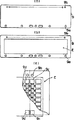
続いて、図1の半導体装置の製造方法の一実施形態について、図3〜図6を参照して説明する。本発明の半導体装置の製造方法は、リードレス表面実装型の半導体装置を可撓性平板状の金属基板上に形成し、金属基板を剥離して製造する製造方法である。 Next, an embodiment of a method for manufacturing the semiconductor device of FIG. 1 will be described with reference to FIGS. The semiconductor device manufacturing method of the present invention is a manufacturing method in which a leadless surface mounting type semiconductor device is formed on a flexible flat metal substrate and the metal substrate is peeled off.
先ず、リードレス表面実装型の半導体装置を製造するにあたり、図3(a)に示した可撓性平板状の金属基板9を用意する。金属基板9は、薄いステンレス鋼板であり、その厚さは、0.1mmである。金属基板9には、金属基板9の自動搬送用の孔9a,9b等が形成され、金属基板9を自動搬送させるための孔が形成され、かつ金属基板9を金型に固定するための孔が形成されている。
First, when manufacturing a leadless surface mounting type semiconductor device, a flexible
図3(b)は、金属基板9に金属層によるパターンが形成され、半導体素子が搭載されるパターンが形成される電着フレームを示している。電着フレームは、金属基板9の片面に搭載された半導体素子を樹脂封止することで、金属基板9の片面に樹脂封止体が形成される。
FIG. 3B shows an electrodeposition frame in which a pattern by a metal layer is formed on the
以下、図4,図5を参照して、半導体装置の製造方法を、第1から第8の工程に大別して説明する。 Hereinafter, with reference to FIG. 4 and FIG. 5, the method for manufacturing a semiconductor device will be roughly classified into first to eighth steps.
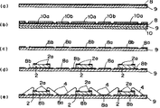
1)第1の製造工程は、図4(a)に示すように、ステンレス鋼板等による平板状の金属基板9の片面側全面に金属層8を電着して成膜する電着工程である。先ず、金属基板9の一面には、スピンコート法によって光感光性のレジストを塗布して、レジスト膜の全面に露光して硬化させる。続いて、マスクを施した金属基板9を電着槽に浸漬し、金属基板9の他面に金属層8を形成する。金属層8は、Ni又はNi・Co合金を電着したNi又はNi・Co合金薄膜層であり、その後、Ni・Co合金薄膜層上には、金をフラッシュ法等による真空蒸着或いはスパッタリング法等によって成膜される。電着工程は、金属基板9と電着槽内の電極間に通電することによって、金属基板9にNi又はNi・Co合金薄膜層の金属層8が形成される。Ni・Co合金薄膜は、例えば20〜35μmの厚さとし、金薄膜層を0.3μmの厚さとする。なお、金属基板9にNi又はNi・Co合金を電着する前に、金を含む合金をフラッシュ法等で真空蒸着することによって、後の電極金属層を形成する成膜工程を省略することができる。
1) The first manufacturing process is an electrodeposition process in which a metal layer 8 is electrodeposited on the entire surface of one side of a
2)第2の製造工程は、金属層8のエッチング工程である。このエッチング工程では、図4(b)に示すように、金属基板9の片側にレジスト膜10によるマスクを形成し、金属基板9の金属層8上には、レジスト膜10a,10bが選択的に形成される。
2) The second manufacturing process is an etching process of the metal layer 8. In this etching step, as shown in FIG. 4B, a mask made of a resist
その後、このエッチング工程では、金属層8を選択的にエッチングして除去する。図4(c)に示したように、金属基板9の片側に金属層8a,8bが形成された電着フレームが形成する。電着フレームには、図3(b)に示したように、半導体素子が搭載されて金線をワイヤーボンディングする領域Eが形成される。領域Eは、金属層8a,8bとがマトリック状に形成されている。図3(c)には、その詳細なパターンを示した。
Thereafter, in this etching step, the metal layer 8 is selectively etched and removed. As shown in FIG. 4C, an electrodeposition frame in which
図3(C)は樹脂封止体裏面の金属基板を剥離した場合におけるワイヤーボンディング領域E裏面のパターンを示す。このパターンには半導体素子が複数封止された樹脂封止体を個々の半導体装置に切断するための切断マーク9d,9cがマーキングされている。切断時には切断マーク9d,9cの間に切断部位が設定させる。
FIG. 3C shows a pattern on the back surface of the wire bonding region E when the metal substrate on the back surface of the resin sealing body is peeled off. This pattern is marked with cutting
3)第3の製造工程は、素子搭載工程である。この工程では、図4(d)に示したように、半導体素子2が、公知の手法によって金属層8bに搭載される。半導体素子2は、図1に示したように、その表面には、電極パッド2aが形成されている。
3) The third manufacturing process is an element mounting process. In this step, as shown in FIG. 4D, the
4)電着フレームに半導体素子2が搭載された後、第4の製造工程のワイヤボンディング工程に進む。第4の製造工程では、図4(e)に示したように、半導体素子2に金ワイヤ4をワイヤボンディングする工程であり、ワイヤ4は、半導体素子2の電極パッド2aと金属層8aとを超音波ボンディング等によって電気的に接続される。
4) After the
5)図4(e)のワイヤボンディング工程に続いて、図5(a)に示した第5の製造工程である樹脂モールド工程に進む。樹脂モールド工程は、図5(a)に示したように、金属基材9に半導体素子2が搭載されて、ワイヤボンディングされた後の電着フレームが、モールド金型(上型)に装着される。モールド金型内には、エポキシ樹脂がモールド金型(上型)に形成されたキャビティ(図示しなし)により圧入される。この樹脂モールドでは、金属基材9が樹脂モールドにおける下型としての機能を果たす。
5) Subsequent to the wire bonding step of FIG. 4E, the process proceeds to a resin molding step which is the fifth manufacturing step shown in FIG. In the resin molding step, as shown in FIG. 5A, the electrodeposition frame after the
なお、半導体素子2が搭載された金属基材9を並列に配置して、エポキシ樹脂がライナを通してそれぞれの金属基材9と上金型との間に圧入することで、半導体素子が搭載された電着フレームを多数樹脂封止することができる。
The
6)樹脂モールド工程の後、第6の製造工程に進む。第6の製造工程は、図5(b)に示した金属基材9の剥離工程である。図5(b)に示したように、樹脂封止体11から金属基材9を引き離す。金属基材9は可撓性のある平板状であるので、樹脂封止体11から容易に剥離することができる。樹脂封止体11の底面には、金属層8a,8bが露出している。金属層8a,8bの露呈面は、樹脂封止体11の底面と面一である。なお、Ni又はNi・Co合金薄膜層が露呈している場合は、剥離工程に続いて、第7の製造工程であるダイシング工程に進む。
6) After the resin molding step, the process proceeds to the sixth manufacturing step. The sixth manufacturing process is a peeling process of the
7)第7の製造工程は、図5(d)に示した樹脂封止体11を切断線Sに沿って切断することで、樹脂封止体を一半導体素子毎に切り出す。樹脂封止体11は、半導体素子2間の金属層8aが中央部から切断されて個々の半導体装置に切り出される。)
7) In the seventh manufacturing process, the
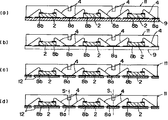
第7の製造工程であるダイシング工程について、図6を参照して説明する。なお、図6(a)は、多数の半導体装置が樹脂封止された樹脂封止体11の一部切欠部斜視図を示しており、同図(b)が樹脂封止体11の裏面を示している。
A dicing process which is a seventh manufacturing process will be described with reference to FIG. FIG. 6A shows a partially cutaway perspective view of the
同図において、S1 ,S2は、切断線(ダイシングライン)を示しており、それぞれ樹脂封止体11に形成されている溝7a,7bを、金属基材9の裏面より切断線S1 ,S2 に沿って切断することにより、各半導体装置に切り分けられる。
In the figure, S 1 and S 2 indicate cutting lines (dicing lines), and the
図6(b)に示した樹脂封止体11の裏面図から明らかなように、電極金属層8aは、切断マークM11とM12との間の切断線S2 に沿って切り出すことによって、隣接する半導体装置がそれぞれの外部導出用の金属層となる。
As is apparent from the rear view of the
更に、隣接する半導体装置の隣接間の金属層8bは、切断マークM21とM22との間の切断線S1 に沿って切り離されている。樹脂封止体11は、ダイシング工程で切断線S1 ,S2に沿って、切断することによって、個々の半導体装置に切り出される。
Furthermore, the
ダイシング工程に続いて電極を形成する第8の製造工程に進む。
8)この第8の製造工程は、図1,2に示すように、切り出された個々の半導体装置の樹脂封止体2の底面の金属層8a,8bに金薄膜層8cをフラッシュ法または電解メッキあるいは無電解メッキは等によって蒸着する。
After the dicing process, the process proceeds to an eighth manufacturing process for forming electrodes.
8) In the eighth manufacturing step, as shown in FIGS. 1 and 2, the gold
なお、電着フレームの形成は、上記の実施形態による製造方法に限定されることなく、金属基板の金または金と他の金属とを混合した薄膜層を形成した後、パターニングして、その後、NiまたはNi・Coの薄膜金属層を電着して形成してもよい。 In addition, the formation of the electrodeposition frame is not limited to the manufacturing method according to the above-described embodiment, and after forming a thin film layer in which gold or gold and another metal are mixed on a metal substrate, patterning is performed, and then A thin film metal layer of Ni or Ni · Co may be formed by electrodeposition.
金属基板の金または金と他の金属を混合した薄膜層は、金属基板の一方の面にレジスト膜を全面に形成して、他方の面にレジスト膜をパターンニングして、半導体素子の搭載部と外部導出用の金属層とを形成する金属基板面を露呈させて、他はレジスト膜で覆って選択的に金薄膜層に電着して形成する。 A thin film layer of gold or a mixture of gold and other metal on a metal substrate is formed by forming a resist film on one surface of the metal substrate and patterning the resist film on the other surface, thereby mounting a semiconductor element mounting portion. And the metal substrate surface on which the metal layer for leading out is exposed, and the others are covered with a resist film and selectively deposited on the gold thin film layer.
その後、パターンニングしたレジスト膜を除去して、金薄膜層が選択的に形成された面、全面にNiまたはNi・Coの薄膜金属層を形成し、続いて、NiまたはNi・Co薄膜金属層を選択的に除去する。 Thereafter, the patterned resist film is removed, and a Ni or Ni · Co thin film metal layer is formed on the entire surface where the gold thin film layer is selectively formed, followed by the Ni or Ni · Co thin film metal layer. Is selectively removed.
このような製造工程を経て、先の実施形態で説明したように、金属基板9に金属層8aと金属層8bとを形成する。その後の製造工程は、先に説明した製造工程と同様であるので説明を省略する。
Through such a manufacturing process, the
無論、本発明の半導体装置では、金属基板として、厚さが0.1mmのステンレス鋼板が用いられているが、この厚さに限定するものではない。しかし、半導体が封止された樹脂封止体から金属基板を剥離するのに好ましい。また、従来、金属基板として、銅板を用いて製造した半導体装置では、銅板をエッチングで除去しなければならいが、ステンレス鋼板を用いることによって、樹脂封止体からステンレス鋼板を容易に剥離することができる。例えば、ステンレス鋼板としては、JIS記号分類によるSUSの何れかが用いられている。 Of course, in the semiconductor device of the present invention, a stainless steel plate having a thickness of 0.1 mm is used as the metal substrate, but the thickness is not limited to this. However, it is preferable for peeling the metal substrate from the resin sealing body in which the semiconductor is sealed. Conventionally, in a semiconductor device manufactured using a copper plate as a metal substrate, the copper plate must be removed by etching, but by using a stainless steel plate, the stainless steel plate can be easily peeled from the resin sealing body. it can. For example, as the stainless steel plate, any of SUS by JIS symbol classification is used.
また、図2に示した半導体装置を製造する場合は、半導体素子2が搭載される金属層8bの厚さを約20μmとするために、金属層8aを金属基板に形成した後、金属層8bを形成するためのレジストマスクを形成して、金属層8aを成膜する時間より長い時間電着槽に浸漬して電着して形成すればよい。その後の製造工程は、先に説明した通りである。
When the semiconductor device shown in FIG. 2 is manufactured, after the
なお、図7の半導体装置の裏面図で示したように、半導体装置は、樹脂パッケージ7から露出する金属層13は、その露呈面は平面形状を有し、樹脂パッケージ7に収納された半導体素子2の電極パッド2aと金属層13とがワイヤ4で電気的に接続されている。
As shown in the rear view of the semiconductor device in FIG. 7, in the semiconductor device, the
上記のように、本発明の半導体装置では、樹脂パッケージに半導体素子が封止されて、樹脂パッケージの底面から外部導出用の金属層が露出しており、樹脂パッケージの底面と外部導出用の金属層の底面とが面一であり、この金属層の面に更に、Ni又はNi・Co合金による薄膜層とAu薄膜層を形成して、外部電極とする。この外部電極は、樹脂パッケージの底面から僅かに突出するのみで、この半導体装置を基板に実装した場合、半導体装置の底面を基板に接触させて実装することができる。 As described above, in the semiconductor device of the present invention, the semiconductor element is sealed in the resin package, and the metal layer for external derivation is exposed from the bottom surface of the resin package. The bottom surface of the layer is flush with the metal layer, and a thin film layer and an Au thin film layer made of Ni or Ni / Co alloy are further formed on the surface of the metal layer to form an external electrode. The external electrode protrudes slightly from the bottom surface of the resin package. When the semiconductor device is mounted on the substrate, the external electrode can be mounted by contacting the bottom surface of the semiconductor device with the substrate.
2 半導体素子
2a 電極パッド
4 ワイヤ
7 樹脂パッケージ
7a,7b 溝
8,8a,8b 金属層
8c 金属層
9 金属基板
10,10a,10b レジスト膜
11 樹脂封止体
12 金薄膜層
13,14 金属層
S,S1 ,S2切断線
E 半導体素子が搭載される領域
Claims (1)
前記金属層は、金属基板の一面にレジスト膜をパターンニングして、金属層を形成する金属基板面を露呈させて、薄膜層を電着して形成した後に薄膜金属層が形成されたものであり、
また、半導体素子が搭載される金属層と外部導出用の金属層の形成領域の外周において、前記金属層の切断マーク間毎に切断部位を設定したことを特徴とする半導体装置の製造方法。 A flexible flat metal substrate, patterned and forming a electrodeposition frame forming a metal layer, a step of mounting adjacent a plurality of semiconductor elements to said metal layer patterned in the electrodeposition frame In addition, the electrode pads of the adjacent semiconductor elements are electrically connected to the metal layer for external derivation formed between the semiconductor elements mounted on the patterned metal layer by providing a predetermined interval with a wire. A wire bonding step, a resin sealing step of resin-sealing a semiconductor element mounted on the electrodeposition frame, a peeling step of peeling the metal substrate to obtain a resin sealing body, and the semiconductor A resin sealing body in which a plurality of elements are sealed has a cutting part set between the cut marks of the patterned metal layer. A method of manufacturing a semiconductor device including a cut-out process of disconnection,
The metal layer is formed by patterning a resist film on one surface of a metal substrate, exposing the metal substrate surface on which the metal layer is to be formed, and electrodepositing the thin film layer, and then forming the thin film metal layer. Yes,
In addition, a method for manufacturing a semiconductor device, characterized in that cutting sites are set between the cutting marks of the metal layer on the outer periphery of the formation region of the metal layer on which the semiconductor element is mounted and the metal layer for leading out.
Priority Applications (1)
| Application Number | Priority Date | Filing Date | Title |
|---|---|---|---|
| JP2006072498A JP3869849B2 (en) | 2000-04-25 | 2006-03-16 | Manufacturing method of semiconductor device |
Applications Claiming Priority (2)
| Application Number | Priority Date | Filing Date | Title |
|---|---|---|---|
| JP2000124102 | 2000-04-25 | ||
| JP2006072498A JP3869849B2 (en) | 2000-04-25 | 2006-03-16 | Manufacturing method of semiconductor device |
Related Parent Applications (1)
| Application Number | Title | Priority Date | Filing Date |
|---|---|---|---|
| JP2001078791A Division JP2002016181A (en) | 2000-04-25 | 2001-03-19 | Semiconductor device, manufacturing method thereof, and electrodeposition frame |
Publications (3)
| Publication Number | Publication Date |
|---|---|
| JP2006196922A JP2006196922A (en) | 2006-07-27 |
| JP2006196922A5 JP2006196922A5 (en) | 2006-09-21 |
| JP3869849B2 true JP3869849B2 (en) | 2007-01-17 |
Family
ID=36802682
Family Applications (1)
| Application Number | Title | Priority Date | Filing Date |
|---|---|---|---|
| JP2006072498A Expired - Lifetime JP3869849B2 (en) | 2000-04-25 | 2006-03-16 | Manufacturing method of semiconductor device |
Country Status (1)
| Country | Link |
|---|---|
| JP (1) | JP3869849B2 (en) |
Families Citing this family (7)
| Publication number | Priority date | Publication date | Assignee | Title |
|---|---|---|---|---|
| JP5098452B2 (en) * | 2007-06-11 | 2012-12-12 | 住友金属鉱山株式会社 | Manufacturing method of semiconductor device |
| JP5151438B2 (en) * | 2007-12-10 | 2013-02-27 | 大日本印刷株式会社 | Semiconductor device and manufacturing method thereof, and substrate for semiconductor device and manufacturing method thereof |
| JP5497030B2 (en) | 2009-06-24 | 2014-05-21 | アオイ電子株式会社 | Semiconductor device and manufacturing method of semiconductor device |
| EP2337068A1 (en) | 2009-12-18 | 2011-06-22 | Nxp B.V. | Pre-soldered leadless package |
| JP5779748B2 (en) | 2010-11-02 | 2015-09-16 | リコー電子デバイス株式会社 | Semiconductor package and electronic component mounting body |
| TWI533380B (en) * | 2011-05-03 | 2016-05-11 | 旭德科技股份有限公司 | Package structure and manufacturing method thereof |
| JP2012084938A (en) * | 2012-02-03 | 2012-04-26 | Sumitomo Metal Mining Co Ltd | Substrate for manufacturing semiconductor device |
-
2006
- 2006-03-16 JP JP2006072498A patent/JP3869849B2/en not_active Expired - Lifetime
Also Published As
| Publication number | Publication date |
|---|---|
| JP2006196922A (en) | 2006-07-27 |
Similar Documents
| Publication | Publication Date | Title |
|---|---|---|
| US6800508B2 (en) | Semiconductor device, its manufacturing method and electrodeposition frame | |
| US5081562A (en) | Circuit board with high heat dissipations characteristic | |
| KR101037997B1 (en) | A semiconductor die package, a substrate for semiconductor die pachage, and a forming method thereof, and a manufacturing method and a processing method of a lead fram structure | |
| US5756377A (en) | Lead frame and manufacturing method thereof | |
| JP3626075B2 (en) | Manufacturing method of semiconductor device | |
| KR100407595B1 (en) | Semiconductor device and method of manufacturing the same | |
| US5859471A (en) | Semiconductor device having tab tape lead frame with reinforced outer leads | |
| KR100400629B1 (en) | Circuit device and method of manufacturing the same | |
| JP3869849B2 (en) | Manufacturing method of semiconductor device | |
| US20050212107A1 (en) | Circuit device and manufacturing method thereof | |
| JP2003017518A (en) | Method for manufacturing hybrid integrated circuit device | |
| US6271057B1 (en) | Method of making semiconductor chip package | |
| JP2005244033A (en) | Electrode package and semiconductor device | |
| JP2004207275A (en) | Circuit device and its manufacturing method | |
| JP3574026B2 (en) | Circuit device and method of manufacturing the same | |
| JP2001217372A (en) | Circuit device and method of manufacturing the same | |
| JP3643743B2 (en) | Mounting board | |
| JP3574025B2 (en) | Circuit device and method of manufacturing the same | |
| JP3668090B2 (en) | Mounting board and circuit module using the same | |
| JP3634709B2 (en) | Semiconductor module | |
| JP2003174121A (en) | Semiconductor device | |
| JP3778783B2 (en) | Circuit device and manufacturing method thereof | |
| JP4036603B2 (en) | Semiconductor device and manufacturing method thereof | |
| JP3691328B2 (en) | Circuit device and circuit module | |
| JP2002237545A (en) | Manufacturing for circuit device |
Legal Events
| Date | Code | Title | Description |
|---|---|---|---|
| A521 | Written amendment |
Free format text: JAPANESE INTERMEDIATE CODE: A523 Effective date: 20060413 |
|
| A621 | Written request for application examination |
Free format text: JAPANESE INTERMEDIATE CODE: A621 Effective date: 20060413 |
|
| A871 | Explanation of circumstances concerning accelerated examination |
Free format text: JAPANESE INTERMEDIATE CODE: A871 Effective date: 20060413 |
|
| RD03 | Notification of appointment of power of attorney |
Free format text: JAPANESE INTERMEDIATE CODE: A681 Effective date: 20060418 |
|
| A521 | Written amendment |
Free format text: JAPANESE INTERMEDIATE CODE: A523 Effective date: 20060509 |
|
| A521 | Written amendment |
Free format text: JAPANESE INTERMEDIATE CODE: A523 Effective date: 20060510 |
|
| A975 | Report on accelerated examination |
Free format text: JAPANESE INTERMEDIATE CODE: A971005 Effective date: 20060629 |
|
| A131 | Notification of reasons for refusal |
Free format text: JAPANESE INTERMEDIATE CODE: A131 Effective date: 20060711 |
|
| A521 | Written amendment |
Free format text: JAPANESE INTERMEDIATE CODE: A523 Effective date: 20060908 |
|
| TRDD | Decision of grant or rejection written | ||
| A01 | Written decision to grant a patent or to grant a registration (utility model) |
Free format text: JAPANESE INTERMEDIATE CODE: A01 Effective date: 20061010 |
|
| A61 | First payment of annual fees (during grant procedure) |
Free format text: JAPANESE INTERMEDIATE CODE: A61 Effective date: 20061013 |
|
| R150 | Certificate of patent or registration of utility model |
Ref document number: 3869849 Country of ref document: JP Free format text: JAPANESE INTERMEDIATE CODE: R150 Free format text: JAPANESE INTERMEDIATE CODE: R150 |
|
| FPAY | Renewal fee payment (event date is renewal date of database) |
Free format text: PAYMENT UNTIL: 20101020 Year of fee payment: 4 |
|
| R250 | Receipt of annual fees |
Free format text: JAPANESE INTERMEDIATE CODE: R250 |
|
| FPAY | Renewal fee payment (event date is renewal date of database) |
Free format text: PAYMENT UNTIL: 20101020 Year of fee payment: 4 |
|
| FPAY | Renewal fee payment (event date is renewal date of database) |
Free format text: PAYMENT UNTIL: 20111020 Year of fee payment: 5 |
|
| R250 | Receipt of annual fees |
Free format text: JAPANESE INTERMEDIATE CODE: R250 |
|
| FPAY | Renewal fee payment (event date is renewal date of database) |
Free format text: PAYMENT UNTIL: 20111020 Year of fee payment: 5 |
|
| FPAY | Renewal fee payment (event date is renewal date of database) |
Free format text: PAYMENT UNTIL: 20121020 Year of fee payment: 6 |
|
| R250 | Receipt of annual fees |
Free format text: JAPANESE INTERMEDIATE CODE: R250 |
|
| FPAY | Renewal fee payment (event date is renewal date of database) |
Free format text: PAYMENT UNTIL: 20121020 Year of fee payment: 6 |
|
| S111 | Request for change of ownership or part of ownership |
Free format text: JAPANESE INTERMEDIATE CODE: R313115 |
|
| FPAY | Renewal fee payment (event date is renewal date of database) |
Free format text: PAYMENT UNTIL: 20121020 Year of fee payment: 6 |
|
| R350 | Written notification of registration of transfer |
Free format text: JAPANESE INTERMEDIATE CODE: R350 |
|
| FPAY | Renewal fee payment (event date is renewal date of database) |
Free format text: PAYMENT UNTIL: 20121020 Year of fee payment: 6 |
|
| FPAY | Renewal fee payment (event date is renewal date of database) |
Free format text: PAYMENT UNTIL: 20131020 Year of fee payment: 7 |
|
| R250 | Receipt of annual fees |
Free format text: JAPANESE INTERMEDIATE CODE: R250 |
|
| R250 | Receipt of annual fees |
Free format text: JAPANESE INTERMEDIATE CODE: R250 |
|
| R250 | Receipt of annual fees |
Free format text: JAPANESE INTERMEDIATE CODE: R250 |
|
| R250 | Receipt of annual fees |
Free format text: JAPANESE INTERMEDIATE CODE: R250 |
|
| R250 | Receipt of annual fees |
Free format text: JAPANESE INTERMEDIATE CODE: R250 |
|
| R250 | Receipt of annual fees |
Free format text: JAPANESE INTERMEDIATE CODE: R250 |
|
| S531 | Written request for registration of change of domicile |
Free format text: JAPANESE INTERMEDIATE CODE: R313531 |
|
| S533 | Written request for registration of change of name |
Free format text: JAPANESE INTERMEDIATE CODE: R313533 |
|
| R350 | Written notification of registration of transfer |
Free format text: JAPANESE INTERMEDIATE CODE: R350 |
|
| R250 | Receipt of annual fees |
Free format text: JAPANESE INTERMEDIATE CODE: R250 |
|
| R250 | Receipt of annual fees |
Free format text: JAPANESE INTERMEDIATE CODE: R250 |
|
| R250 | Receipt of annual fees |
Free format text: JAPANESE INTERMEDIATE CODE: R250 |
|
| EXPY | Cancellation because of completion of term |