JP3854905B2 - Liquid crystal display - Google Patents
Liquid crystal display Download PDFInfo
- Publication number
- JP3854905B2 JP3854905B2 JP2002220606A JP2002220606A JP3854905B2 JP 3854905 B2 JP3854905 B2 JP 3854905B2 JP 2002220606 A JP2002220606 A JP 2002220606A JP 2002220606 A JP2002220606 A JP 2002220606A JP 3854905 B2 JP3854905 B2 JP 3854905B2
- Authority
- JP
- Japan
- Prior art keywords
- liquid crystal
- crystal display
- signal line
- display panel
- voltage
- Prior art date
- Legal status (The legal status is an assumption and is not a legal conclusion. Google has not performed a legal analysis and makes no representation as to the accuracy of the status listed.)
- Expired - Fee Related
Links
Images


Classifications
-
- H—ELECTRICITY
- H04—ELECTRIC COMMUNICATION TECHNIQUE
- H04M—TELEPHONIC COMMUNICATION
- H04M1/00—Substation equipment, e.g. for use by subscribers
- H04M1/02—Constructional features of telephone sets
- H04M1/0202—Portable telephone sets, e.g. cordless phones, mobile phones or bar type handsets
- H04M1/026—Details of the structure or mounting of specific components
- H04M1/0266—Details of the structure or mounting of specific components for a display module assembly
-
- G—PHYSICS
- G02—OPTICS
- G02F—OPTICAL DEVICES OR ARRANGEMENTS FOR THE CONTROL OF LIGHT BY MODIFICATION OF THE OPTICAL PROPERTIES OF THE MEDIA OF THE ELEMENTS INVOLVED THEREIN; NON-LINEAR OPTICS; FREQUENCY-CHANGING OF LIGHT; OPTICAL LOGIC ELEMENTS; OPTICAL ANALOGUE/DIGITAL CONVERTERS
- G02F1/00—Devices or arrangements for the control of the intensity, colour, phase, polarisation or direction of light arriving from an independent light source, e.g. switching, gating or modulating; Non-linear optics
- G02F1/01—Devices or arrangements for the control of the intensity, colour, phase, polarisation or direction of light arriving from an independent light source, e.g. switching, gating or modulating; Non-linear optics for the control of the intensity, phase, polarisation or colour
- G02F1/13—Devices or arrangements for the control of the intensity, colour, phase, polarisation or direction of light arriving from an independent light source, e.g. switching, gating or modulating; Non-linear optics for the control of the intensity, phase, polarisation or colour based on liquid crystals, e.g. single liquid crystal display cells
- G02F1/133—Constructional arrangements; Operation of liquid crystal cells; Circuit arrangements
-
- G—PHYSICS
- G09—EDUCATION; CRYPTOGRAPHY; DISPLAY; ADVERTISING; SEALS
- G09G—ARRANGEMENTS OR CIRCUITS FOR CONTROL OF INDICATING DEVICES USING STATIC MEANS TO PRESENT VARIABLE INFORMATION
- G09G3/00—Control arrangements or circuits, of interest only in connection with visual indicators other than cathode-ray tubes
- G09G3/20—Control arrangements or circuits, of interest only in connection with visual indicators other than cathode-ray tubes for presentation of an assembly of a number of characters, e.g. a page, by composing the assembly by combination of individual elements arranged in a matrix no fixed position being assigned to or needed to be assigned to the individual characters or partial characters
- G09G3/34—Control arrangements or circuits, of interest only in connection with visual indicators other than cathode-ray tubes for presentation of an assembly of a number of characters, e.g. a page, by composing the assembly by combination of individual elements arranged in a matrix no fixed position being assigned to or needed to be assigned to the individual characters or partial characters by control of light from an independent source
- G09G3/36—Control arrangements or circuits, of interest only in connection with visual indicators other than cathode-ray tubes for presentation of an assembly of a number of characters, e.g. a page, by composing the assembly by combination of individual elements arranged in a matrix no fixed position being assigned to or needed to be assigned to the individual characters or partial characters by control of light from an independent source using liquid crystals
- G09G3/3611—Control of matrices with row and column drivers
- G09G3/3622—Control of matrices with row and column drivers using a passive matrix
- G09G3/3644—Control of matrices with row and column drivers using a passive matrix with the matrix divided into sections
-
- G—PHYSICS
- G09—EDUCATION; CRYPTOGRAPHY; DISPLAY; ADVERTISING; SEALS
- G09G—ARRANGEMENTS OR CIRCUITS FOR CONTROL OF INDICATING DEVICES USING STATIC MEANS TO PRESENT VARIABLE INFORMATION
- G09G3/00—Control arrangements or circuits, of interest only in connection with visual indicators other than cathode-ray tubes
- G09G3/20—Control arrangements or circuits, of interest only in connection with visual indicators other than cathode-ray tubes for presentation of an assembly of a number of characters, e.g. a page, by composing the assembly by combination of individual elements arranged in a matrix no fixed position being assigned to or needed to be assigned to the individual characters or partial characters
- G09G3/34—Control arrangements or circuits, of interest only in connection with visual indicators other than cathode-ray tubes for presentation of an assembly of a number of characters, e.g. a page, by composing the assembly by combination of individual elements arranged in a matrix no fixed position being assigned to or needed to be assigned to the individual characters or partial characters by control of light from an independent source
- G09G3/36—Control arrangements or circuits, of interest only in connection with visual indicators other than cathode-ray tubes for presentation of an assembly of a number of characters, e.g. a page, by composing the assembly by combination of individual elements arranged in a matrix no fixed position being assigned to or needed to be assigned to the individual characters or partial characters by control of light from an independent source using liquid crystals
- G09G3/3611—Control of matrices with row and column drivers
- G09G3/3648—Control of matrices with row and column drivers using an active matrix
- G09G3/3666—Control of matrices with row and column drivers using an active matrix with the matrix divided into sections
-
- G—PHYSICS
- G09—EDUCATION; CRYPTOGRAPHY; DISPLAY; ADVERTISING; SEALS
- G09G—ARRANGEMENTS OR CIRCUITS FOR CONTROL OF INDICATING DEVICES USING STATIC MEANS TO PRESENT VARIABLE INFORMATION
- G09G3/00—Control arrangements or circuits, of interest only in connection with visual indicators other than cathode-ray tubes
- G09G3/20—Control arrangements or circuits, of interest only in connection with visual indicators other than cathode-ray tubes for presentation of an assembly of a number of characters, e.g. a page, by composing the assembly by combination of individual elements arranged in a matrix no fixed position being assigned to or needed to be assigned to the individual characters or partial characters
- G09G3/34—Control arrangements or circuits, of interest only in connection with visual indicators other than cathode-ray tubes for presentation of an assembly of a number of characters, e.g. a page, by composing the assembly by combination of individual elements arranged in a matrix no fixed position being assigned to or needed to be assigned to the individual characters or partial characters by control of light from an independent source
- G09G3/36—Control arrangements or circuits, of interest only in connection with visual indicators other than cathode-ray tubes for presentation of an assembly of a number of characters, e.g. a page, by composing the assembly by combination of individual elements arranged in a matrix no fixed position being assigned to or needed to be assigned to the individual characters or partial characters by control of light from an independent source using liquid crystals
- G09G3/3611—Control of matrices with row and column drivers
- G09G3/3696—Generation of voltages supplied to electrode drivers
-
- G—PHYSICS
- G02—OPTICS
- G02F—OPTICAL DEVICES OR ARRANGEMENTS FOR THE CONTROL OF LIGHT BY MODIFICATION OF THE OPTICAL PROPERTIES OF THE MEDIA OF THE ELEMENTS INVOLVED THEREIN; NON-LINEAR OPTICS; FREQUENCY-CHANGING OF LIGHT; OPTICAL LOGIC ELEMENTS; OPTICAL ANALOGUE/DIGITAL CONVERTERS
- G02F1/00—Devices or arrangements for the control of the intensity, colour, phase, polarisation or direction of light arriving from an independent light source, e.g. switching, gating or modulating; Non-linear optics
- G02F1/01—Devices or arrangements for the control of the intensity, colour, phase, polarisation or direction of light arriving from an independent light source, e.g. switching, gating or modulating; Non-linear optics for the control of the intensity, phase, polarisation or colour
- G02F1/13—Devices or arrangements for the control of the intensity, colour, phase, polarisation or direction of light arriving from an independent light source, e.g. switching, gating or modulating; Non-linear optics for the control of the intensity, phase, polarisation or colour based on liquid crystals, e.g. single liquid crystal display cells
- G02F1/133—Constructional arrangements; Operation of liquid crystal cells; Circuit arrangements
- G02F1/1333—Constructional arrangements; Manufacturing methods
- G02F1/1345—Conductors connecting electrodes to cell terminals
- G02F1/13456—Cell terminals located on one side of the display only
-
- H—ELECTRICITY
- H04—ELECTRIC COMMUNICATION TECHNIQUE
- H04M—TELEPHONIC COMMUNICATION
- H04M1/00—Substation equipment, e.g. for use by subscribers
- H04M1/02—Constructional features of telephone sets
- H04M1/0202—Portable telephone sets, e.g. cordless phones, mobile phones or bar type handsets
-
- H—ELECTRICITY
- H04—ELECTRIC COMMUNICATION TECHNIQUE
- H04M—TELEPHONIC COMMUNICATION
- H04M2250/00—Details of telephonic subscriber devices
- H04M2250/16—Details of telephonic subscriber devices including more than one display unit
Landscapes
- Engineering & Computer Science (AREA)
- Physics & Mathematics (AREA)
- General Physics & Mathematics (AREA)
- Chemical & Material Sciences (AREA)
- Crystallography & Structural Chemistry (AREA)
- Theoretical Computer Science (AREA)
- Computer Hardware Design (AREA)
- Nonlinear Science (AREA)
- Signal Processing (AREA)
- Optics & Photonics (AREA)
- Mathematical Physics (AREA)
- Liquid Crystal (AREA)
- Control Of Indicators Other Than Cathode Ray Tubes (AREA)
- Liquid Crystal Display Device Control (AREA)
- Devices For Indicating Variable Information By Combining Individual Elements (AREA)
Description
【0001】
【発明の属する技術分野】
本発明は、液晶表示装置に係わり、特に、携帯型表示装置に用いられる液晶表示装置の駆動回路に適用して有効な技術に関する。
【0002】
【従来の技術】
STN(Super Twisted Nematic)方式の液晶表示装置、あるいはTFT(Thin Film Transistor)方式の液晶表示装置は、ノート型パソコン等の表示装置として広く使用されている。これらの液晶表示装置は、液晶表示パネルと、液晶表示パネルを駆動する駆動回路を備えている。
【0003】
そして、このような液晶表示装置は、携帯電話機等の携帯用端末装置の表示装置としての使用が急速に増加している。液晶表示装置を携帯用端末装置の表示装置として用いる場合には、従来の液晶表示装置に比べて、さらに低コスト化、小型化、高画質化、低消費電力化が望まれる。さらに、液晶表示装置を携帯電話機等の表示装置として利用する場合に、1台の携帯電話機に2枚の液晶表示パネルを搭載したものが実用化されている。
【0004】
【発明が解決しようとする課題】
携帯電話機等の携帯用端末装置の表示装置は、画像付きメール等の普及に伴い、画像表示機能のさらなる向上が望まれている。また、1台の携帯電話機に2枚の液晶表示パネルを搭載した場合にも、2枚の液晶表示パネル両方共に、高画質、高精細化等、高い画像表示機能が求められている。また、携帯端末であることから低消費電力化が求められており、さらには、コスト競争力の強化も重要な課題である。
【0005】
携帯端末装置の小型化に伴う問題点として、液晶表示装置の駆動回路を実装するスペースが減少することがあげられる。さらに、実装方法に関して、携帯端末装置では、装置の中心線と表示画面の中心とが重なる配置方法である所謂画面センター化の要望があり、駆動回路を実装する位置が制限され、配置に考慮が必要である。さらには、従来の液晶表示装置では、表示画面の隣合う2辺に駆動回路が設けられていたが、1辺にのみ駆動回路を実装する所謂3辺フリー化の強い要望もある。また、実装面積の縮小及び、低コスト化のために、実装部品の削減の必要もある。
【0006】
特に、1台の携帯電話機に2枚の液晶表示パネルを搭載した場合に、それぞれの液晶表示パネルに、駆動回路や各種部品を設ける必要があり、実装面積が増加するといった問題が生じていた。
【0007】
さらに、携帯電話機のように不特定多数の利用者による使用が想定される機器では、通常とは異なる使用方法がとられた場合にも安定した動作が望まれている。そのため、携帯電話機の電源である電池が抜け落ちた場合等の不測の事態にも、画面に残像が表示されず、通常に電源をオフとした場合に近い動作が要求されている。
【0008】
本発明は、前記従来技術の問題点を解決するためになされたものであり、本発明の目的は、小型の液晶表示装置を用いる機器において、2枚の液晶表示パネルを搭載した場合に、最適な駆動回路を実現する技術を提供することにある。
【0009】
本発明の前記ならびにその他の目的と新規な特徴は、本明細書の記述及び添付図面によって明らかにする。
【0010】
【課題を解決するための手段】
本願において開示される発明のうち、代表的なものの概要を簡単に説明すれば、下記の通りである。
【0011】
2枚の液晶表示パネルと、駆動回路とを備える液晶表示装置であって、駆動回路を一方の液晶表示パネルに搭載し、該駆動回路が搭載された液晶表示パネルの1辺に出力端子を設け、前記出力端子と他方の液晶表示パネルとを配線で接続することで、前記駆動回路により2枚の液晶表示パネルを駆動するとともに、前記駆動回路から2枚の液晶表示パネルそれぞれに適した共通電圧が出力され、前記他方の液晶表示パネルには前記配線を介して共通電圧が供給される。
【0012】
さらに、駆動回路は、2つの液晶表示パネルに最適な共通電圧を供給するために、2つの共通電圧を出力可能な電源回路を有する。
【0013】
【発明の実施の形態】
以下、図面を参照して本発明の実施の形態を詳細に説明する。なお、実施の形態を説明するための全図において、同一機能を有するものは同一符号を付け、その繰り返しの説明は省略する。
【0014】
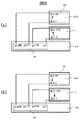
図1は、本発明の実施の形態の液晶表示装置の基本構成を示すブロック図である。同図に示すように、本実施の形態の液晶表示装置は、第1の液晶表示パネル1と、第2の液晶表示パネル200と、駆動回路50とから構成される。これらの液晶表示パネルを携帯電話機に用いる場合には、第1の液晶表示パネル1はメインパネルとして用いられ、第2の液晶表示パネル200は機器の背面に設けられるサブパネルとして用いられる。
【0015】
第1の液晶表示パネル1及び第2の液晶表示パネル200には複数の走査信号線(またはゲート信号線)GLと映像信号線(またはドレイン信号線)DLとが、各々並列して設けられている。走査信号線GLと映像信号線DLとの交差する部分に対応して画素部11が設けられる。複数の画素部11はマトリックス状に配置され(図示せず)表示領域8及び、表示領域9を形成している。各画素部11には、画素電極12と薄膜トランジスタ10が設けられている。この画素電極12、薄膜トランジスタ10等が設けられたTFT基板2と、カラーフィルタ等が形成されるフィルタ基板(図示せず)とを、所定の間隙を隔てて重ね合わせて液晶表示パネルが形成される。両基板間の周縁部には枠状にシール材が設けられており、両基板を貼り合わせると共に、シール材の一部に設けた液晶封入口から両基板間のシール材の内側に液晶が封入、封止される。
【0016】
従来、サブパネルの主な使用目的は文字を表示することであった。そのため、サブパネルには画質の劣る液晶表示パネルが用いられていた。しかしながら、サブパネルがカメラ付携帯電話機においてファインダーとして使用されるなど、サブパネルにもメインパネル同様の画質が要求されている。そのため、本発明では第2の液晶表示パネル200もTFT方式の液晶表示パネルを用いることとした。
【0017】
従って、第1の液晶表示パネル1および、第2の液晶表示パネル200共に画素部に薄膜トランジスタ10が設けられている。各画素の薄膜トランジスタ10は、ソースが画素電極12に接続され、ドレインが映像信号線DLに接続され、ゲートが走査信号線GLに接続される。この薄膜トランジスタ10は、画素電極12に表示電圧(階調電圧)を供給するためのスイッチとして機能する。画素電極12と対向電極15との間に電圧を印加することにより、液晶分子の配向方向等が変化し、それに伴い液晶層の光に対する性質が変化することを利用して表示が行われる。TFT方式の液晶表示パネルは、薄膜トランジスタ10がスイッチとして働き、画素電極12に電圧を保持する方式であることから、コントラストが高い等、高画質の液晶表示パネルが実現できる。
【0018】
なお、ソース、ドレインの呼び方は、バイアスの関係で逆になることもあるが、ここでは、映像信号線DLに接続される方をドレインと称する。また、本実施の形態は、対向電極15がTFT基板2に設けられる所謂横電界方式の液晶表示パネルにも、対向電極15がフィルタ基板に設けられる所謂縦電界方式の液晶表示パネルにも同様に適用される。
【0019】
液晶表示パネル1および、液晶表示パネル200を駆動、表示するように、走査信号線GL、映像信号線DLと、対向電極15には、駆動回路50から信号が供給される。駆動回路50は、液晶表示パネル1のTFT基板2を構成する透明性の絶縁基板(ガラス基板、樹脂基板等)に搭載(または形成)される。また、駆動回路50は、TFT基板2に設けられた映像信号線DL、走査信号線GL、第1の液晶表示パネル用の対向電極配線16、第2の液晶表示パネル用の対向電極配線17とに電気的に接続されている。なお、駆動回路50は、半導体集積回路(LSI)であるが、TFT基板2とは別の基板に形成される場合は、TFT基板2に直接搭載されるか、TCP(Tape Carrier Package)により搭載される。また、TFT基板2と同じ基板に直接形成された半導体回路により構成されることも可能である。
【0020】
駆動回路50は、映像信号線DLに階調電圧を供給し、走査信号により薄膜トランジスタ10のオン・オフを制御して、画素電極12に階調電圧を書き込むように働き、さらに対向電極15に共通電圧を供給する。また、駆動回路50はコントローラの機能を有しており、外部のCPU等(図示せず)から信号が供給されている。そのため、入力端子34が設けられ、外部からの信号が入力端子34を介して入力し駆動回路50に供給される。外部から入力したクロック信号、ディスプレイタイミング信号、水平同期信号、垂直同期信号等の各表示制御信号および表示用デ−タ(R・G・B)を基に、駆動回路50は液晶表示パネルを制御・駆動する信号を作成する。
【0021】
以下簡単に駆動回路50の動作を説明すると、駆動回路50は、外部信号からフレーム開始指示信号(FLM、以下スタート信号とも呼ぶ)およびシフトクロック(CL1)を形成し、1水平走査時間(以下1Hとも呼ぶ)毎に、順次液晶表示パネル1及び液晶表示パネル200の各走査信号線GLにHighレベルの選択走査電圧(走査信号)を供給する。これにより、液晶表示パネル1及び液晶表示パネル200の各走査信号線GLに接続された複数の薄膜トランジスタ10が、1水平走査時間1Hの間導通する。
【0022】
また、駆動回路50は画素が表示すべき階調に対応する階調電圧を映像信号線DLに出力する。薄膜トランジスタ10がオン状態になると、映像信号線DLから階調電圧(映像信号)が画素電極12に供給される。その後、薄膜トランジスタ10がオフ状態となることで画素が表示すべき映像に基づく階調電圧が画素電極12に保持される。
【0023】
駆動回路50は液晶表示パネル1だけではなく、液晶表示パネル200も駆動している。そのため、駆動回路50が設けられた液晶表示パネル1から液晶表示パネル200へも信号が供給される。符号21は走査信号の出力端子で配線25により液晶表示パネル200側の入力端子27に接続されている。そのため、液晶表示パネル1には、液晶表示パネル200の走査信号を供給するために配線35が形成されている。また、符号22は映像信号用の出力端子であり、液晶表示パネル200に供給される階調電圧が、この出力端子22から出力する。そのため、駆動回路50に接続された映像信号線DLは表示領域8内の薄膜トランジスタ10に接続されるだけではなく、さらに、表示領域8外にまで延在して出力端子22にも接続されている。
【0024】
なお、液晶表示パネル200に設けられた映像信号線DLの数に比べて、液晶表示パネル1の映像信号線DLの数が多い場合には、液晶表示パネル200に接続されない映像信号線DLが存在する。図1では、映像信号線DLn+1以降が液晶表示パネル200に接続されないが、それらの映像信号線は、配線容量が液晶表示パネル200に接続される映像信号線DLn等と異なる。そのため、液晶表示パネル200に接続されない映像信号線には、配線容量調整素子24が設けられている。
【0025】
液晶表示パネル1と液晶表示パネル200とを駆動する方法は、例えば、液晶表示パネル1の走査信号線GL1−1から始まり、順に走査信号線GL1−mまで走査して、さらに続けて液晶表示パネル200の走査信号線GL2−1から走査信号線GL2−kまで走査するといった、あたかも1枚の液晶表示パネルを駆動するかのような方法が可能である。このとき、映像信号線DLには階調電圧が出力されるが、走査信号線GL2−1からGL2−kまでが走査されている間には、液晶表示パネル1に設けられた映像信号線DLにも、液晶表示パネル200に供給される階調電圧が出力される。
【0026】
また、駆動回路50には、対向電極15に第1の液晶表示パネル用の対向電極配線16と、第2の液晶表示パネル用の対向電極配線17とが電気的に接続されている。液晶表示パネル1には対向電極配線16に接続された出力端子23が設けられ、出力端子23と液晶表示パネル200に設けられた入力端子29とが配線25で接続される。
【0027】
本願発明が適用される液晶表示装置においては、液晶層に印加する電圧の極性を周期的に反転させる交流化駆動が行われている。交流化駆動を行う目的は直流電圧が液晶に印加されることによる劣化を防止するためである。ただし、交流化駆動を行っても微小な直流成分が液晶層に印加される場合が生じる。そのような場合に、対向電極に印加される共通電圧を調整して直流成分を解消する。そのため、各液晶表示パネル毎に最適な共通電圧値が設定されることとなる。
【0028】
前述したように、液晶表示パネル1と液晶表示パネル200とは、同じ駆動回路50によって駆動されているが、直流成分が生じる原因は画素電極12と対向電極15とに印加される電圧の差だけではないため、同じ駆動回路50により駆動されても液晶表示パネル1と液晶表示パネル200とに生じる直流成分は微妙に異なる。そのため、液晶表示パネル1と液晶表示パネル200には個別に最適な共通電圧が供給される。
【0029】
最適な共通電圧が設定されていないと、表示にはフリッカという現象が発生し、著しく表示品質を低下させる。駆動回路50からは液晶表示パネル1用と液晶表示パネル200用の2つの共通電圧が出力可能となっており、また2つの共通電圧の微調整が可能である。そのため、各液晶表示パネルのフリッカが減少するようにそれぞれの共通電圧を個別に微調整することで、液晶表示パネル1用と液晶表示パネル200用の2つの最適な共通電圧が供給可能となり、フリッカ等の表示品質の低下を防ぐことができる。
【0030】
図1に示す液晶表示装置では、液晶表示パネル1と液晶表示パネル200とを、共通の駆動回路50によって駆動可能とすることで、駆動回路を実装する面積の削減による小型化や、部品の共通化による低コスト化が可能となっている。また、液晶表示パネル1と液晶表示パネル200とに、共通の信号を出力するだけではなく、2つの液晶表示パネルに特有な共通電圧を出力することで、2つの液晶表示パネルを同じ駆動回路で駆動しても良好な表示が可能である。
【0031】
次に、図2に液晶表示パネル1と液晶表示パネル200とをフレキシブル基板26を用いて接続した概略平面図を示す。フレキシブル基板26には接続端子が設けられており、液晶表示パネル1に設けられた出力端子21、22、23および、液晶表示パネル200に設けられた入力端子27、28、29とに異方性導電膜等を用いて電気的に接続されている。このフレキシブル基板26により各出力端子、入力端子との間が電気的に接続され、液晶表示パネル1と液晶表示パネル200との間で信号が伝達可能になっている。
【0032】
なお、各端子は狭ピッチで多数並設されており、図示することが困難なため、図中、各端子は両端の端子を示し、各端子の記載は省略している。また、携帯電話機ではフレキシブル基板を折り曲げて、液晶表示パネル1と液晶表示パネル200とを導光板の表裏に設ける利用形態がとられるが、図をわかり易くするために、液晶表示パネル1と液晶表示パネル200とを同一平面に記載した。
【0033】
図2において、液晶表示パネル1に搭載された駆動回路50は、走査信号線駆動回路58と映像信号線駆動回路57とに分割された場合を示している。液晶表示パネル1にはサブパネル走査信号用配線35が設けられており、走査信号線駆動回路58から出力したサブパネル走査信号用配線35は、走査信号用出力端子21に接続している。さらに走査信号用出力端子21からは液晶表示パネル200に供給される走査信号が出力し、フレキシブル基板26を介して液晶表示パネル200の入力端子27に走査信号が伝達される。液晶表示パネル200には走査信号用配線36が設けられており、入力端子27から各走査信号線GLに接続している。なお、液晶表示パネル1用にも同様に走査信号用配線36が設けられており、液晶表示パネル1の下辺に設けられた走査信号線駆動回路58から各走査信号線GLとの間を接続している。
【0034】
また、走査信号線駆動回路58からは、液晶表示パネル1用の対向電極配線16と、液晶表示パネル200用の対向電極配線17とが出力し、映像信号線駆動回路57とTFT基板2との間を通るように配線されている。対向電極配線16は液晶表示パネル1の対向電極に接続され、対向電極配線17はTFT基板2の走査信号用配線36が設けられた辺と対向する辺(図中右側の辺)に沿って配線され、出力端子23に接続されている。さらに、液晶表示パネル200用の対向電極配線17は、フレキシブル基板26を介して液晶表示パネル200の対向電極に接続されている。
【0035】
図2では、液晶表示パネル200の表示領域9と駆動回路50との間には、液晶表示パネル1の表示領域8が存在するため、液晶表示パネル200を駆動する配線は、サブパネル走査信号用配線35のように、表示領域8の周囲に設けられることとなる。ただし、映像信号線DLは液晶表示パネル1と液晶表示パネル200とで共通に利用されることで、表示領域8内に配線され、さらに表示領域8外まで延在させて液晶表示パネル200まで配線可能となっている。なお、表示装置としては、表示領域以外の部分の面積は小さい方が良いため、表示領域周囲のサブパネル走査信号用配線35等が設けられる領域もできる限り小さくなるように考慮されている。
【0036】
符号30はフレキシブル基板で、駆動回路50に入力する信号、電源電圧等が供給されている。また、符号51はコンデンサで駆動回路50の昇圧回路等で用いられる。また、符号56は可変抵抗器で共通電圧の微調整に用いられる。
【0037】
なお、映像信号線駆動回路57からは、液晶表示パネル200に階調電圧が出力されており、映像信号線DL(2)により液晶表示パネル1に階調電圧を供給すると共に、液晶表示パネル200にも階調電圧を供給している。液晶表示パネル200の中心線43と、液晶表示パネル1との中心線44とがなるべく重なるように、液晶表示パネル200にも階調電圧を供給する映像信号線DL(2)は液晶表示パネル1の中央部の映像信号線が用いられている。そのため、映像信号線DL(2)が設けられる領域の両端に、液晶表示パネル200に接続されない映像信号線DL(1)が設けられている。
【0038】
フレキシブル基板25は柔軟な素材からなり、折り曲げることが可能である。そのため、フレキシブル基板25を折り曲げ、液晶表示パネル1と液晶表示パネル200とは、1枚の導光板を挟んで、該導光板の2つの面にそれぞれ設けられることが可能である。また、フレキシブル基板25には折り曲げ易いように、スリット39が設けられている。
【0039】
図3に、液晶表示パネル1用の走査信号線駆動回路58と液晶表示パネル200用走査信号線駆動回路59とが映像信号線駆動回路57を挟んで設けられる実施例を示す。図中左側の液晶表示パネル1の辺には、走査信号用配線36が設けられ走査信号線駆動回路58と各走査信号線GLとの間を接続している。また、液晶表示パネル1の右側の辺にはサブパネル走査信号用配線35が設けられており、走査信号線駆動回路59から出力したサブパネル走査信号用配線35は、走査信号用出力端子21に接続している。さらに走査信号用出力端子21からは液晶表示パネル200に供給される走査信号が出力し、フレキシブル基板26を介して液晶表示パネル200の入力端子27に走査信号が伝達される。
【0040】
図3に示すように、走査信号線駆動回路58と走査信号線駆動回路59とを映像信号線駆動回路57を挟んで設けると、表示領域8の左右両端部に走査信号用配線36とサブパネル走査信号用配線35とを別々に設けることができる。また、走査信号線駆動回路58と走査信号線駆動回路59と映像信号線駆動回路57とは、1つの駆動回路50として一体に形成することも可能である。
【0041】
なお、図示していないが、走査信号線駆動回路58からは液晶表示パネル1用の共通電圧と、走査信号線駆動回路59からは液晶表示パネル200用の共通電圧が出力しており、それぞれの液晶表示パネルに最適な共通電圧が供給されている。
【0042】
図4に、フレキシブル基板26に駆動回路50を搭載し、液晶表示パネル1と液晶表示パネル200との間に設ける実施例を示す。駆動回路50からは、図中下側へ液晶表示パネル1用の信号と、図中上側へ液晶表示パネル200用の信号が出力する。
【0043】
駆動回路50が、液晶表示パネル1の表示領域8と液晶表示パネル200の表示領域9との間に設けられているため、液晶表示パネル1に設けられる液晶表示パネル200用の信号配線が省略可能で、液晶表示パネル1にはサブパネル走査信号用配線35が設けられていない。そのため、配線領域が減少し小型化が可能である。また、フレキシブル基板26にはコンデンサ51、可変抵抗器56等の部品も搭載されている。符号38は外部接続用配線部で、外部機器に接続されるように外部に伸びている。このため、入力用のフレキシブル基板が兼用となり、部品点数も減少している。
【0044】
図4に示す駆動回路50においては、1つの出力から、図中下側へ配線され液晶表示パネル1に接続されると共に、同じ出力から図中上側へ配線され液晶表示パネル200に接続することで、1つの出力を共通に利用することが可能である。ただし、液晶表示パネル1用と液晶表示パネル200用とに別々の出力を形成しても良い。さらに、フレキシブル基板26上に液晶表示パネル1用の駆動回路と、液晶表示パネル200用の駆動回路として、複数の駆動回路を搭載することも可能である。
【0045】
なお、図示していないが、駆動回路50からは液晶表示パネル1用の共通電圧と、液晶表示パネル200用の共通電圧が出力しており、それぞれの液晶表示パネルに最適な共通電圧が供給されている。
【0046】
図5に、液晶表示パネル1の液晶表示パネル200側の辺に駆動回路50を搭載する実施例を示す。図4と同様に駆動回路50は液晶表示パネル1の表示領域8と液晶表示パネル200との間に設けられており、駆動回路50からは、図中下側へ液晶表示パネル1用の信号と、図中上側へ液晶表示パネル200用の信号とが出力する。また、図4と同様に液晶表示パネル1に設けられる液晶表示パネル200用の信号配線が省略可能で、液晶表示パネル1にはサブパネル走査信号用配線35が設けられていない。
【0047】
図5に示す駆動回路50においても、1つの出力から、図中下側へ配線され液晶表示パネル1に接続されると共に、同じ出力から図中上側へ配線され液晶表示パネル200に接続することで、1つの出力を共通に利用することが可能である。また、液晶表示パネル1用と液晶表示パネル200用とに別々の出力を形成することも可能である。
【0048】
なお、図示していないが、駆動回路50からは液晶表示パネル1用の共通電圧と、液晶表示パネル200用の共通電圧が出力しており、それぞれの液晶表示パネルに最適な共通電圧が供給されている。
【0049】
次に図6、図7を用いて、走査信号線駆動回路58の出力の順番と、走査信号線GLとの関係を示す。まず、図6(a)に示すように、液晶表示パネル1の走査信号線の数が176本で、液晶表示パネル200の走査線数が64本の場合、走査信号線駆動回路58は、出力数が240で出力go1から出力開始して、順番に走査信号線GL1−1からGL1−176を走査し、さらに、GL1−176の次にGL2−1を走査して、最後に出力go240により走査信号線GL2−64を走査する駆動方法を用いることができる。
【0050】
なお、液晶表示パネル1と液晶表示パネル200のどちらか一方のみを表示する場合や、両パネルの一部のみ表示する場合などでは、走査信号線駆動回路58及び、映像信号線駆動回路57が共通のため、非表示部も電圧を印加することになる。そのため、非表示部も交流化駆動する必要があり表示部同様に、極性の異なる信号が供給される。
【0051】
例えば、液晶表示パネル1が非表示の場合でも、走査信号線GLの数が240本のため、1画面(1フレーム)を50Hzで表示している場合では、1走査信号線(1ライン)あたり50×240=12kHzのライン周波数となる。しかし、実際に表示しているのは64ラインだけであり50×64=3.2kHzで充分である。非表示にもかかわらず高い駆動周波数でデータの書き換えを行うことになり、低消費電力の妨げになってしまう。
【0052】
そこで、非表示部の走査信号線の走査を一括して行うこととした。例えば、液晶表示パネル1が非表示の場合、走査信号線GL1−1からGL1−176を1水平走査期間1H(または、数Hでも可)同時に走査し、その後、走査信号線GL2−1から走査信号線GL2−64を通常に走査することとした。同様に液晶表示パネル200が非表示の場合や、両パネルの一部のみ表示する場合にも一括走査することで、低消費電力化が図れる。
【0053】
次に、図6(b)のように、液晶表示パネルの配置によっては、液晶表示パネル200を先に走査する必要も生じる。このような場合には、出力go240から出力開始し、最初に走査信号線GL2−64を走査し、最後に出力go1から走査信号線GL1−1を走査することとになる。
【0054】
走査信号線駆動回路58は図6(a)に示す走査順と、図6(b)に示す走査順とを区別するために、インストラクション信号等を設け、順方向と逆方向とに走査方向を設定する。このとき、出力数が240以上の場合では、インストラクション信号等により出力開始位置の設定や有効出力数の設定を行う。
【0055】
次に、図7に示すように液晶表示パネル1と液晶表示パネル200との走査方向が異なる場合を示す。この場合には、走査信号線駆動回路58を走査信号線駆動部58−aと58−bとに分けて、それぞれ、順方向と逆方向に走査方向を設定する。また、先に走査開始する側を設定し、一方の走査終了を待って他方が走査開始するようにする。
【0056】
また、符号ga177に示すように、走査信号線に接続されないで余る出力がある場合には、走査信号線駆動部58−aの有効走査数を176に設定し、走査信号線駆動部58−bはカウンタ等で176回走査されるのをカウントして、走査信号線駆動部58−aの走査終了を知ることとする。なお、出力数に対して走査信号線の数が不一致である理由は、駆動回路50が複数の形式の液晶表示パネルに対応可能であるようにするためである。すなわち、走査信号線の数が異なる複数の液晶表示パネルにも汎用的に対応可能とするためである。
【0057】
図7(b)では、走査信号線駆動部58−aは出力開始が2で、有効走査数を176で、走査方向が逆方向に設定されている。走査信号線駆動部58−aは走査信号線駆動部58−bによる走査数をカウントしており、走査信号線駆動部58−bの有効走査数64がカウントされるのを待って、出力ga176(逆方向で2番目の出力)から出力を開始する。
【0058】
このように、2枚の液晶表示パネルを駆動する場合には、その配置により走査方向や順番が複数選択可能であり、それぞれの場合に対応するために、インストラクション信号等により走査方向や順番等が設定可能になっている。
【0059】
次に、昇圧回路について説明する。携帯電話機等の小型携帯機器では、電源として電池の利用が一般的である。また、流通量の多さから電池は出力電圧が1.5V程度から4V程度のものが利用される。
【0060】
そのため、昇圧回路を用いて液晶表示装置用に電源電圧を作成している。図8に薄膜トランジスタ方式の液晶表示装置に必要な電源電圧を示す。なお、図8では液晶表示パネル1及び、200の対向電極15に供給する共通電圧VCOMを一定周期で反転させる、所謂共通電圧反転駆動方式を用いている場合の各駆動電圧を示している。
【0061】
図8においてVGONは画素部の薄膜トランジスタ10(TFT)をオンするための走査信号VGのハイ電圧で、約7.5V程度が必要となる。また、VGOFFは薄膜トランジスタをオフするための電圧であり、走査信号VGのロウ電圧で、約−5.5V程度必要となる。VGHは走査信号VGを出力する走査信号線駆動回路58(ゲートドライバ)用ハイ電源で、VGLは走査信号線駆動回路58用ロウ電源である。走査信号のハイ電圧VGONが約7.5Vなので、VGHは8V、走査信号のロウ電圧VGOFFが約−5.5Vなので、VGLは−6V程度必要となる。
【0062】
次に、VDHは階調基準電圧である。階調基準電圧VDHを基準に映像信号線駆動回路(ソースドライバ)57で階調電圧を生成する。液晶材の特性から5.0V程度が必要である。DDVDHは駆動回路50用の電源電圧である。映像信号線駆動回路57が出力する階調電圧の基準電圧VDHが5.0Vで、映像信号線駆動回路57の最大定格が6.0Vであるため、5.5V程度が必要となる。
【0063】
VCOMHは対向電極用ハイ電圧で、VCOMLは対向電極用ロウ電圧である。VCOMHは5.0V以下が必要となり、VCOMLは−2.5V程度の電圧が必要となる。VCLは対向電極用電圧生成電源で、対向電極用ロウ電圧VCOMLを生成するための電源電圧である。VCOML生成回路の動作マージンを考慮し−3V程度が必要となる。
【0064】
以上液晶表示装置に必要な電源の中で、駆動回路50用の電源電圧DDVDHと、走査信号線駆動回路58用ハイ電源VGHと、走査信号線駆動回路58用ロウ電源VGLと、対向電極用電圧生成電源VCLとをチャージポンプ方式の昇圧回路を用いて作成することとし、他の電圧は昇圧回路で形成した電圧を分圧等して形成することとした。
【0065】
チャージポンプ方式の昇圧回路の動作原理について図9を用いて、2倍昇圧を例に取り簡単に説明する。昇圧回路は入力電源Vin、昇圧容量C11、保持容量Cout1、切り替えスイッチSW−1、SW−2で構成され、切り替えスイッチにより図9(a)の充電状態と、図9(b)の放電状態を実現している。
【0066】
まず図9(a)の充電状態では切り替えスイッチSW−1により、昇圧容量C11の一方の電極をGND電位に接続し、スイッチSW−2により昇圧容量C11の他方の電極を入力電源Vinに接続して、昇圧容量C11を入力電源Vinに対し並列に接続する。これにより入力電源Vin分の電荷が昇圧容量C11に充電される。
【0067】
次に図9(b)では、切り替えスイッチSW−3により、図9(a)において昇圧容量C11のGND電位に接続された電極に、入力電源Vinを印加するよう直列に接続する。この時、昇圧容量C11の他方の電極は、入力電源Vinの2倍の電圧である2×Vinとなる。スイッチSW−4により昇圧容量C11、入力電源Vinに対し並列にCout1を接続する。これにより保持容量Cout1には2×Vinの電圧が保持される。
【0068】
次に、図9に示す昇圧回路で、前述の映像信号線駆動回路57用の電源電圧DDVDH(約5.5V)と、走査信号線駆動回路58用ハイ電源VGH(約7.5V)と、走査信号線駆動回路58用ロウ電源VGL(約−6V)と、対向電極用電圧生成電源VCL(約−3V)とを作成する場合を検討する。なお、携帯電話機では入力電源Vinは電源電池の出力電圧である場合が多いが、本明細書では電源電池の出力電圧も含めて昇圧回路に供給される電圧を意味するものとする。
【0069】
入力電源Vinを3Vとすると、映像信号線駆動回路57用の電源電圧DDVDH(約5.5V)は約2倍なので、入力電源Vinを2倍とする昇圧回路が必要である。走査信号線駆動回路58用ハイ電源VGH(約7.5V)は2倍では不足なので、入力電源Vinを3倍とする昇圧回路が必要である。走査信号線駆動回路58用ロウ電源VGLは約−6Vなので、入力電源Vinを−2倍とする昇圧回路が必要で、対向電極用電圧生成電源VCLは約−3Vなので、入力電源Vinを−1倍とする昇圧回路が必要となる。
【0070】
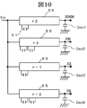
図10に入力電源Vinを2倍、3倍、−2倍、−1倍とする昇圧回路55の構成を示す。なお、−2倍、−1倍とする場合では、厳密には昇圧ではないが、ここでは、昇圧回路を入力電圧から異なる電圧を形成する回路の意味で用いる。コンデンサ51の数は、入力電源Vinを2倍にする回路で1個、3倍にする回路で2個、−2倍にする回路で2個、−1倍にする回路で1個の合計6個必要である。このように、図10に示す回路では、回路の外付部品としてコンデンサ51を多数使用しており、実装部品点数が多くなり、実装面積が広くなってしまうといった問題がある。なお、図中の符号Cout1からCout4は出力電圧を保持する保持容量である。
【0071】
次に、図11に昇圧回路55の出力を入力電源として利用し、一部の外付けコンデンサ51を共用とすることで、外付けコンデンサ51の数を減らす回路の概念ブロック図を示す。図11に示す回路では、外付けコンデンサとして、昇圧回路52に接続している外付けコンデンサC11と、昇圧回路53に接続している外付けコンデンサC12、C21の3個が必要であり、図10に示す回路に対して外付けコンデンサの数を6個から3個に減少することができる。なお、外付けコンデンサC11は2倍用で、外付けコンデンサC12は3倍用と−1倍用との共用で、外付けコンデンサC21は−2倍用である。
【0072】
図12を用いて図11に示す昇圧回路53において、入力電源Vinを3倍に昇圧する動作を説明する。図12(a)では、入力電源電圧Vinを用い、昇圧容量(外付けコンデンサ)C12を充電している。また、図12(b)は昇圧回路52を示しており、図9で説明したように入力電源電圧Vinの2倍である電圧DDVDHが作成されている。図12に示す回路では、入力電源電圧Vinを2倍に昇圧した電圧DDVDHを利用することで、外付けコンデンサの数を省略している。図12(c)に示すように、保持容量Cout1の出力である電圧DDVDHを用い、保持容量Cout1と昇圧容量C12とを直列につなぐことで、入力電源Vinの3倍の電圧が作成される。
【0073】
次に、図13を用いて入力電源Vinを−1倍にする動作を説明する。図13(a)では、入力電源Vinを用いて、昇圧容量C12を電圧Vinに充電する。その後、図13(b)では、昇圧容量C12の正極性側の電極をGND電位に接続することで、入力電源Vinと極性が反転した電圧VCLを作成している。そして昇圧容量C12と保持容量Cout4を並列につなぐことで、保持容量Cout3に入力電源Vinを−1倍した電圧VCLが保持される。図13に示す回路では、図12の3倍に昇圧する回路で用いた外付けコンデンサC12を共用することで数を減らしている。
【0074】
次に、図14を用いて入力電源Vinを−2倍にする動作を説明する。図14(a)では、昇圧回路52の保持容量Cout1の出力である電圧DDVDHを用いて、昇圧容量C21を電圧DDVDHに充電する。その後、図14(b)では、昇圧容量C21の正極性側の電極をGND電位に接続することで、電圧DDVDHと極性が反転した電圧VGLを作成している。そして昇圧容量C21と保持容量Cout4を並列につなぐことで、保持容量Cout4に入力電源Vinを−2倍した電圧VGLが保持される。
【0075】
このように、図11に示す昇圧回路では、保持容量Cout1に保持されている昇圧した電圧を利用することで、コンデンサを省略し部品数を減少させている。さらに、図13、図14に示す回路では、負極性側の電圧をコンデンサの接続を逆転することと、保持容量の昇圧された電圧に加えて入力電源Vinを利用することで、コンデンサを兼用可能として部品数を減少させている。このコンデンサの数を省略可能としたり、兼用可能としているのは、液晶表示装置特有の電源が映像信号線駆動回路57用の電源電圧DDVDHと走査信号線駆動回路58用ハイ電源VGHと、走査信号線駆動回路58用ロウ電源VGLと、対向電極用電圧生成電源VCLのように複数あり、また、負極性側の電圧があるためである。そのため昇圧容量C12、C21、C22を時分割で、複数の昇圧回路の間で兼用することや、昇圧した電圧を利用することが可能となっている。
【0076】
図15に図11に示す昇圧回路53のより具体的な構成を示し、以下図16に示すタイミングチャートを用いて動作を説明する。まず、電圧VGHを作成するために、図12に示した動作を実現する方法について説明する。図12(a)に示す回路とするには、図15のスイッチSW1とスイッチSW3をオンにする。スイッチSW1とスイッチSW3をオンにすると、昇圧容量C12には入力電源Vinの電圧が充電される。この時、図12(b)に示す回路のように、昇圧回路52からは電圧DDVDHが出力している。次に、図12(c)に示す回路となるように、図15のスイッチSW1、スイッチSW3をオフとし、スイッチSW4をオンにして、昇圧容量C12に電圧DDVDHを印加すると同時に、スイッチSW8をオンにして、保持容量Cout2を充電する。このようにして、保持容量Cout2には入力電源Vinの3倍の電圧が保持される。
【0077】
次に、図13に示した回路の動作について説明する。図13(a)に示す回路となるように、図15のスイッチSW1、スイッチSW3をオンにして、昇圧容量C12を入力電源Vinで充電する。次に、スイッチSW1、スイッチSW3をオフにし、スイッチSW2をオンにして極性を反転させ、さらにスイッチSW9をオンにして保持容量Cout4を充電する。このようにして、保持容量Cout3には入力電源Vinの−1倍の電圧が保持される。
【0078】
次に、図14に示した回路の動作について説明する。図14(a)に示す回路となるように、図15のスイッチSW5、スイッチSW7をオンにして、昇圧容量C21を電圧DDVDHで充電する。次に、スイッチSW5、スイッチSW7をオフにし、スイッチ6をオンにして極性を反転させ、さらにスイッチSW10をオンにして保持容量Cout4を充電する。
【0079】
以上述べたように、図15に示す回路は、昇圧容量C12、C21を時分割で兼用している。また、図16に示すように、昇圧容量C12、C21は、スイッチSW1、SW3、SW5、SW7により繰り返し充電され、スイッチSW4、SW8により昇圧動作に使用されると共に、スイッチSW2、SW9、SW6、SW10により反転(昇圧)動作にも使用される。このように昇圧容量C12、C21を時分割で兼用することで、外付けコンデンサの数が減少し、液晶表示装置の部品点数が削減される。
【0080】
図15に示す昇圧回路で、設定した電圧を出力するには充分であるが、出力する電圧を変更することが困難である。携帯電話機が広く普及することに伴い、用いられる液晶表示パネルは多種多様となり、求められる電圧も多様な値となっている。また、コストダウンの要求も強く昇圧回路も汎用品であることが望まれている。
【0081】
そこで、図17に示す回路のようにスイッチの切換により、昇圧回路の倍率を変更可能とした。倍率の変更はインストラクション信号等により設定可能である。
【0082】
以下、図18から図21により図17に示す回路の動作を説明する。図18は走査信号線駆動回路58用ハイ電源VGHを入力電源Vinの4倍の電圧とする場合の動作を説明する概略回路図である。なお、電圧DDVDHは入力電源Vinの2倍の電圧が昇圧回路52により準備されているものとする。
【0083】
図17に示す回路のスイッチSW5をオンとして、コンデンサC21の一方の電極に電圧DDVDHを印加し、スイッチSW7をオンとしてコンデンサC21の他方の電極を接地電位に接続すると、図18(a)に示す回路となる。その後、スイッチSW5とSW7をオフとし、スイッチSW11とSW17とをオンとすることで、図18(b)の回路となり、コンデンサCout2には入力電源Vinの4倍の電圧が保持される。
【0084】
次に図19に、走査信号線駆動回路58用ハイ電源VGHを入力電源Vinの5倍の電圧とする場合の動作を説明する概略回路図を示す。図19(a)でコンデンサC12に入力電源Vinの電圧を保持し、図19(b)ではコンデンサC21に電圧DDVDHを保持し、図19(c)ではコンデンサC12とコンデンサC21と電圧DDVDHとを直列に接続して、入力電源Vinの5倍の電圧を得ている。なお、スイッチSW16によりコンデンサC12とコンデンサC21とが直列に接続されている。
【0085】
次に図20に、走査信号線駆動回路58用ハイ電源VGHを入力電源Vinの6倍の電圧とする場合の動作を説明する概略回路図を示す。ただし、図20に示す回路では、図20(b)に示すように、コンデンサC22が追加されることで、昇圧可能な電圧値が増加している。図20(c)ではコンデンサC21とコンデンサC22とをスイッチSW19で直列に接続し、さらにコンデンサ22と電圧DDVDHとをスイッチSW15により直列に接続して、入力電源Vinの6倍の電圧を得ている。
【0086】
次に図21に、走査信号線駆動回路58用ロウ電源VGLを入力電源Vinの−5倍の電圧とする場合の動作を説明する概略回路図を示す。ただし、図21(a)ではコンデンサC12に電源Vinの電圧が保持され、図21(b)ではコンデンサC21に電圧DDVDHが保持され、図21(c)ではコンデンサC22に電圧DDVDHが保持される様子を示す。図21(d)では各電圧を保持したコンデンサを逆極性に直列に接続することで、入力電源Vinの−5倍の電圧を得ている。このように、外付けコンデンサを直列に接続することで、何倍もの電圧を得ることが可能である。
【0087】
ただし、図21に示す回路では、全ての外付けコンデンサを同時に直列につないでいるため、一度に一つの電圧しか得ることができないという問題が生じる。そのため、複数の電圧を得るために時分割で使用することになるが、時分割で使用する場合には、供給可能な電流値が減少するという問題も生じる。
【0088】
また、本願発明者は対向電極用電圧生成電源VCLの駆動能力が不足する不具合が生じることを見出した。そこで、図17で示す昇圧回路から対向電極用電圧生成電源VCLが出力可能なままで、さらに対向電極用電圧生成電源VCL専用の昇圧回路を追加することとした。すなわち、対向電極用電圧生成電源VCLに大きな駆動能力が必要な場合には、専用昇圧回路を用い。対して対向電極用電圧生成電源VCLに大きな駆動能力が不要な場合は、外付けコンデンサの少ない昇圧回路が選択可能な構成とした。
【0089】
図22に対向電極用電圧生成電源VCL専用の昇圧回路を示す。図22に示す回路では外付けコンデンサは、C3−1とC3−2の2つが接続可能とした。スイッチSW3−1とSW3−3をオンとしてコンデンサC3−1に入力電源Vinの電圧を保持し、その後、極性を逆転するようにスイッチSW3−2をオンとし、さらにスイッチSW3−7を介してコンデンサCout5に接続することで、入力電源Vinの−1倍の電圧を得ることができる。
【0090】
さらに、外付けコンデンサC3−2を備えることで、スイッチC3−4とC3−5によりコンデンサC3−2にも入力電源Vinの電圧を保持し、その後、コンデンサC3−1とC3−2とをスイッチSW3−6を介して直列に接続し、スイッチSW3−8によりコンデンサCout5に接続することで、入力電源Vinの−2倍の電圧を得ることができる。以上、図15、17、22で説明した回路では、液晶表示パネルに必要な電圧に応じて、昇圧回路の倍率を選択することが可能であり、適宜必要なコンデンサ、スイッチを設けることで、必要な電圧を得ることが可能である。
【0091】
次に、図23を用いて駆動回路50の電源回路部4について説明する。図23は電源回路部4の概略ブロック図である。符号81はメインパネル用対向電極電圧出力回路で、82はレベル調整回路で、83はサブパネル用対向電極電圧出力回路で、84はレギュレータで、86は内部基準電圧生成回路で、87は基準電圧出力回路で、Mは交流化信号入力端子である。電源VCCは駆動回路50の電源電圧で入力電源Vin同様に電池からの出力電圧が入力している。
【0092】
前述したように交流化駆動が行われ、交流化駆動を行う一つの方法として、いわゆるコモン反転駆動方法を行う。図23に示す回路では、コモン反転駆動が可能なように、メインパネル用対向電極電圧出力回路81とサブパネル用対向電極電圧出力回路83とは、一定周期で反転する電圧が出力可能に構成されている。メインパネル用対向電極電圧出力回路81とサブパネル用対向電極電圧出力回路83とには交流化信号線42により交流化信号が伝えられており、交流化信号により対向電極高レベル電圧VCOMHと対向電極低レベル電圧VCOMLが出力する。図24にメインパネル用対向電極高レベル電圧VCOMH−1とメインパネル用対向電極低レベル電圧VCOML−1と、サブパネル用対向電極高レベル電圧VCOMH−2とサブパネル用対向電極低レベル電圧VCOML−2とを有する対向電極電圧の出力波形を示す。
【0093】
なお、振幅調整回路82で基準電圧幅を定め、半固定抵抗88によりメインパネル用対向電極電圧出力回路81とサブパネル用対向電極電圧出力回路83とのそれぞれの電圧を微調整することが可能である。
【0094】
図23に示す回路では、レギュレータ84から、対向電極高レベル電圧VCOMHとしてレベル調整回路82に基準電圧が供給されている。レベル調整回路82では半固定抵抗88により微調整された基準電圧を、対向電極電圧としてメインパネル用対向電極電圧出力回路81の高レベル出力部81aと、サブパネル用対向電極電圧出力回路83の高レベル出力部83aとに出力している。また、レベル調整回路82では、最適な振幅となるように、振幅基準電圧を作成し、対向電極高レベル電圧VCOMHから振幅基準電圧を減算することで、対向電極低レベル電圧VCOMLを作成し、メインパネル用対向電極電圧出力回路81の低レベル出力部81bと、サブパネル用対向電極電圧出力回路83の低レベル出力部83bとに出力している。メインパネル用対向電極電圧出力回路81は交流化信号に従い、高レベル出力部81aと低レベル出力部81bとの接続を切換て、対向電極高レベル電圧VCOMH−1と対向電極低レベル電圧VCOML−1とを出力している。また、サブパネル用対向電極電圧出力回路83は交流化信号に従い、高レベル出力部83aと低レベル出力部83bとの接続を切換て、対向電極高レベル電圧VCOMH−2と対向電極低レベル電圧VCOML−2とを出力する。
【0095】
なお、メインパネル用対向電極電圧出力回路81とサブパネル用対向電極電圧出力回路83とレベル調整回路82では、コントローラからの制御により、対向電極の基準電圧と振幅基準電圧の電圧値を変更可能になっている。図23に示す回路では、昇圧回路54は対向電極用電圧生成電源VCL専用の昇圧回路である。また、昇圧回路52は外付けコンデンサをC1−1とC1−2の2つ備えており、電圧DDVDHとして、入力電源Vinの電圧の2倍と3倍の電圧が出力可能となっている。また、走査信号線GLを保持容量の一方の電極として使用する場合には、対向電極電圧出力回路81、82と同様に走査信号オフ用回路89を設けて、走査信号のロウ側の電圧VGOFFについても高レベル側VGOFFHと低レベル側VGOFFLとが出力可能とする。
【0096】
図23に示す回路では、対向電極用電圧生成電源VCL専用の昇圧回路54を設けるとともに、昇圧回路53は対向電極用電圧生成電源VCLの出力を停止可能としている。昇圧回路53による電源VCLの駆動能力が不足した場合には、対向電極用電圧生成電源VCL専用の昇圧回路54を動作させることが可能である。さらに、画質が低くても充分な場合には、昇圧回路53及び54から電源VCLの出力を停止して、対向電極電圧出力回路81、82からは対向電極高レベル電圧VCOMHを出力し、対向電極低レベル電圧VCOMLは出力しないことで、省電力化が可能である。
【0097】
なお、図23に示す昇圧回路54では、外付けコンデンサC3−2(図中点線で示した)を設けずに、外付けコンデンサC3−1を用いた−1倍の昇圧用のみの出力となっている。このように、液晶表示パネルによっては不要な昇圧電圧もあるため、設ける必要の無いコンデンサは部品点数を削減するために省略される。また、図22に示したスイッチSW3−4、SW3−5等についても駆動回路50として不要な場合は、設けられない場合もある。すなわち、小型化、省電力のために実装部品数や回路規模は、駆動する液晶表示パネルに対して最適なものが選択される。駆動回路50はインストラクション信号等により各液晶表示パネルに対応した設定が行われ、各々の液晶表示パネルに最適な駆動を行うことが可能である。
【0098】
次に、昇圧回路を用いて電源電圧を作成する際の問題点について説明する。昇圧回路を用いて電源電圧を作成する場合には、携帯電話機の電源投入時には電源電圧が所定の電圧となってない。そのため、駆動回路50の内部では図25に示すような電源電圧の状態となる。81は寄生PNPバイポーラであり、82は寄生NPNバイポーラである。これら寄生バイポーラによりNPNPサイリスタとPNPNサイリスタが構成されており、Vin−DDVDH間電圧と、GND−VGL間電圧が、サイリスタの閾値VFを超え、Vin<DDVDH、VGL>GNDのような電位の逆転現象が発生するとサイリスタをオフすることができなくなる。しかしながら、電源投入時では電源VGLはGND電位以上の電位となり、駆動回路5の電源電圧VDHも入力電源Vin以下の電位となってしまう。そのため、Vin−GND間で大電流が流れサイリスタをオフできない、ラッチアップの現象が発生する。
【0099】
そこで、図25に示すようにラッチアップすることを阻止するため、ショートスイッチ76と77を設ける。図26(a)に各電源間にショートスイッチを設けた構成と図26(b)にショートスイッチをオンした場合の等価回路を示す。図26(b)に示すようにショートスイッチは抵抗成分を持つため、電位逆転現象を引き起こす可能性を有している。そのため、外付けダイオード78を用いて、GND−VGL間電圧をサイリスタの閾値VFを超えないように固定した。ただし、液晶表示パネルに設けられた配線では、配線抵抗値が大きく寄生バイポーラを流れる電流を外付けダイオードでは吸収できない不具合も生じる。このため、さらに電位逆転現象を起こさないよう電源オンシーケンスを考慮することとした。
【0100】
図27(a)に電源オンシーケンスを示す。なお、図26(b)に示すように電源DDVDHと電源VGHとの間は、低抵抗スイッチ81と高抵抗スイッチ85の2つからなっている。まず、期間Aにおいて電源DDVDHと電源Vinとのショートスイッチ82をオフとし、電源DDVDHと電源VGH間のショートスイッチ81をオンとして、図23に示した昇圧回路52を動作させ、電源DDVDHを起動する。この時、電源DDVDHと電源VGH間のショートスイッチ81がオンしているため、電源VGHのレベルは電源DDVDHのレベルとなる。なお、上記期間Aにおける動作は、後述するインストラクション信号のAPビットにより設定される。
【0101】
次に、期間Bにおいて昇圧回路53を動作させ電源VGHと電源VGLとを起動する。なお、電源VCLは電源VGLとの電位逆転を防ぐために、遅延させる。または、この時点でVGH>DDVDHとなっているので、電源VGLとVCLとを同時に動作させることも可能である。以上の電源オンシーケンスにより、それぞれの電位が逆転せずに電源を起動でき電源回路の起動マージンを増やすことが可能となる。期間Bにおける動作はインストラクション信号のPONビットにより設定される。
【0102】
次に電源オフシーケンスについて説明する。携帯電話機等では電池抜け等による突然の元電源の遮断により、画面上に残像が発生する不具合があった。そのため、前記残像を回避するために、電源オフシーケンスが必要となった。図27(b)に電源オフシーケンスを示す。まず時点Dにおいて、何らかの理由で入力電源Vinから電圧の供給が止まったとする。期間Cにおいて、電源DDVDH、VCL、VGLは電源起動時前の状態に放電する。また、対向電極電圧VCOM出力および、映像信号線出力もGNDレベルとする。ここで、画素に充電された電荷が放電されるためには、薄膜トランジスタ10をオン状態にしておく必要がある。したがって、薄膜トランジスタ10をオン状態にしておくため、電源VGHは他の電源にたいして放電を遅らせることとする。なお、図28で説明するリセット信号により駆動回路50にリセットがかかると、駆動回路50は後述するインストラクション信号のGONビットの値を設定して走査信号線への全出力をハイレベルとする。
【0103】
電源オンシーケンスでは電源DDVDHと電源VGH間は低抵抗であることが望ましく、対して電源オフシーケンスでは電源VGHは放電を遅らせるために、高抵抗であることが望ましい。そこで、電源オン時と電源オフ時とを駆動回路50に認識させるために、パワーオンリセット信号を利用する。パワーオンリセット信号の波形を図28(a)に示す。パワーオンリセット信号は、オン時には電源投入後、数ms後に立ち上がる仕様とし、数msのロウ期間で駆動回路50をリセットし、その後信号が立ち上がり駆動回路50のリセットを解除する。このとき、駆動回路50としてはリセットは解除されるが、駆動回路内部の状態は確定され、一義的に状態が決まる。
【0104】
対して電源オフ時には各電源端子に接続している容量によって、各電源の放電の状態を異ならせてリセットを行う。図28(b)に示す回路のコンデンサCA1の容量をコンデンサCA2の容量よりも小さくして、RESET信号が電源電圧VCCよりも先に立ち下がる仕様とする。上記構成とすると、電源遮断時に電源VCCに電荷が残った状態で、RESET信号がたち下がることで、駆動回路50にリセットをかけることが可能となる。なお、電源電圧VCCは駆動回路50に外部から供給されている電源電圧である。
【0105】
このように、RESET信号を利用して電源のオンとオフを認識することが可能であるが、RESET状態では駆動回路50はリセット動作に入り、内部の状態は一義的に固定されてしまう。そのため、RESET信号を利用してオンとオフとを認識するために、電源電圧DDVDHとVGHとの間にレベルセンス回路を設けた。
【0106】
図29にレベルセンス回路79を含めた回路で、低抵抗スイッチ81と高抵抗スイッチ85のオン・オフを制御する回路を示す。なお、低抵抗スイッチ81と高抵抗スイッチ85とは、図26で示した電源電圧DDVDHとVGHとの間をショートするスイッチである。また、符号RESETはリセット信号で、符号APは図27(a)の期間Aであることを示す信号で、符号SLPはスリープモード信号で、電源回路の動作を停止して表示を非表示とする信号であり、符号PONは電源VGH、VGL、VCLの出力・停止を示す信号で、図27(a)の期間Bであることを示す信号である。
【0107】
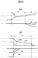
図29に示すレベルセンス回路79はVGH>DDVDHである場合に電圧VGHを出力し、VGH<DDVDHの場合には電圧VGLを出力する。図27に示すように、電源オン時にはVGH<DDVDHで電源オフ時にはVGH>DDVDHであることから、低抵抗スイッチ81は電源オン時にオンで、オフ時にオフとなり、高抵抗スイッチ85は電源オフ時にオンとなる。なお、図29の回路では、高抵抗スイッチ85は電源オン時にもオンとなるが、電源オン時は低抵抗スイッチ81がオンとなっているため、電源VGHと電源DDVDH間の抵抗は、低抵抗スイッチ81が支配的である。そのため、必ずしも高抵抗スイッチ85がオフである必要はなく、図29に示すレベルセンス回路79を用いることができる。
【0108】
図30にパワーオンリセット信号の立ち上がりの波形について示す。パワーオンリセット信号が発振器の始動期間に立ち上がる場合に、波形は図30(a)に示すように安定しないことがある。このため、駆動回路50が誤動作することがあった。そこで、誤動作を防止するため、ローパスフィルタを駆動回路内に設けることとした。図30(b)に示すように駆動回路50内部にローパスフィルタを設けリセット信号にのるノイズを低減する。図30ではローパスフィルタは走査信号線駆動回路58に設けられており、出力端子RESEToutから映像信号線駆動回路57に伝えられる。
【0109】
次に図31を用いて、ミラー用液晶について説明する。図31において符号1は液晶表示パネルで、表示に用いられる。液晶表示パネル1を観察する側には、ミラー用液晶パネル400が設けられている。ミラー用液晶パネル400は、透過偏光軸可変部410と、反射型偏光部420と、吸収型偏光部415とを有している。
【0110】
透過偏光軸可変部410は、入射した直線偏光の光が透過する際にその偏光軸を変化させる状態と、変化させない状態に制御が可能である。図31(a)のように、1対の基板411と基板412に形成した電極間に、電源416から電圧を印加していない場合では、入射した直線偏光の光はその偏光軸が変化し、反射型偏光部420を透過して液晶表示パネル1に到達する。逆に液晶表示パネル1から出射する光が、反射型偏光部420を透過する直線偏光であれば、液晶表示パネル1から出射する光は、ミラー用液晶パネル400を透過して観察者まで到達する。
【0111】
対して、図31(b)の基板411と基板412に形成した電極間に、電圧を印加した場合では、透過偏光軸可変部410に入射した直線偏光の光はその偏光軸が変化しないため、反射型偏光部420で反射する。また、液晶表示パネル1から出射した光は、反射型偏光部420を透過する直線偏光であれば、吸収型偏光部415で吸収され、観察者まで到達しない。
【0112】
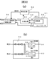
なお、ミラー用液晶パネル400に印加する電圧は、液晶表示パネル1と同様に交流化駆動する。そのために、駆動回路50にはミラー用液晶パネル駆動回路94が設けられる。図32(a)にミラー液晶用回路の全体構成図を示す。ミラー液晶用回路からはミラー用液晶パネル駆動信号MCLKが出力している。ミラー用液晶パネルは液晶に問題が発生しない程度に遅い周波数で駆動することが可能で、ミラー用液晶パネル駆動回路93は省電力のために、低周波駆動される。ただし、コントローラ等から送られてくる信号OSCは高周波のためミラー用液晶パネル駆動回路93は分周回路を備えている。
【0113】
図32(a)において、ミラー液晶用回路は発振器92とそのクロックを分周する分周回路93と昇圧回路52とミラー液晶用駆動回路94を有する。分周回路93ではコントローラからの信号S1によって、昇圧回路52の動作用クロックのS2とミラー液晶用駆動回路用のクロックS3とを生成する。昇圧回路52はミラー液晶用駆動回路94に電源DDVDHを供給する。また、コントローラからの信号S4によって、ミラー液晶駆動用のクロックMCLK+と、クロックMCLK−の出力を制御する。
【0114】
次に図32(b)にミラー液晶用駆動回路94を示す。クロックMCLK+とクロックMCLK−はクロックS3の周期で出力し、クロックMCLK+に対してクロックMCLK−は出力レベルが反転している。
【0115】
ミラー液晶パネルは対向電極間にある電圧が印加されることで、光を反射する状態となる。クロックMCLK+をミラー液晶パネルの一方の電極に印加し、クロックMCLK−をミラー液晶パネルの一方の電極に印加する。DC電圧を印加すると液晶の焼き付き現象が生じるため、交流化する必要がある。振幅はHigh側が電源DDVDH、Low側がGNDとなるようにする。なぜならば、この構成が昇圧回路の使用を最小とすることが出来るので、もっとも消費電力が小さいことが検討の結果わかったからである。なお、ミラー液晶パネルを駆動する電圧のレベルは使用する液晶のしきい値によって異なるため、しきい値の低い液晶にも対応するために、電源DDVDHのレベル(約5V)に加えて、入力電源電圧Vinのレベル(約3V)も使用可能な構成とした。
【0116】
次に、ミラー液晶の表示状態と、クロックMCLK+とクロックMCLK−との出力のレベルと各電源のレベルを説明する。まず、ミラー液晶不使用時(光を透過する時)はクロックMCLK+とクロックMCLK−とのどちらもGNDレベルとする。これは液晶にDC電圧がかからないようにするためである。制御は図32(a)の信号S4で行い、信号S4がHighレベルの時にクロックMCLK+とクロックMCLK−の出力はGNDとなる。これは図32(b)の回路で実現できる。ミラー液晶使用時(光を反射する時)は、クロックMCLK+とクロックMCLK−とのHigh側レベルがDDVDHレベルとVinレベルとの両方の電圧が出力可能とした。
【0117】
High側レベルは図32(b)の回路の電源電圧と同じことから、コントローラから信号S5で昇圧回路52を制御し、図32(b)の回路に入力する電源DDVDHの電圧値を制御する。Vinレベルの時は、図26(a)に示すショートスイッチ81、82、83、84をショートし、さらに昇圧回路はすべて昇圧動作を停止する。これにより図26(a)に示す回路で、ショートスイッチ82がオンしているため、電源DDVDHの電圧は電源Vinと同じ電圧値となり、図32に示す回路の電源DDVDHは電源Vinと同じ電圧値となる。そのため電源電圧はミラー液晶駆動に必要なVinレベルのみ存在し、低消費電力化がはかれ、かつショートスイッチにより各レベルの逆転等はなく安定した動作が出来る。
【0118】
次にDDVDHレベルの時は、図26(a)の81、83、84をショートし、昇圧回路52を動作させる。これによりミラー液晶駆動に必要なDDVDHレベルを生成し、その他の昇圧回路を停止させることで、低消費電力化が図れ、かつショートスイッチにより各電源レベルの逆転等はなく安定した動作が出来る。
【0119】
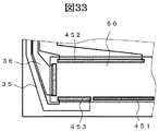
次に、図33に駆動回路50の端子配置を示す。符号451は入力端子領域で、452は液晶表示パネル(メインパネル)1用の走査信号線端子領域で、453は液晶表示パネル(サブパネル)200用の走査信号線端子領域である。走査信号線端子領域452と453とは、駆動回路50のサブパネル走査信号用配線35と走査信号用配線36とが設けられる側の2辺に集中させて設けられている。対して、入力端子領域451はフレキシブル基板30が接続される側に集中して設けられている。また、フレキシブル基板30には外付けコンデンサが搭載されるため、同じ入力端子領域451には外付けコンデンサと接続される端子も設けられている。
【0120】
本願発明の液晶表示装置では、2枚の液晶表示パネルの配置によりその走査方法を変更したり、昇圧回路の倍率を変更するために、インストラクション信号を用いる。図34にインストラクション信号の例を示す。図34に示すインストラクション信号は16ビットからなるシリアルデータを示している。図中横方向に並んだ16ビットの信号がインストラクション信号として外部から駆動回路50に伝えられる。図中縦方向に6つインストラクション信号を並べて示しているが、図34のインストラクション信号では、D15からD13までの3ビットがインデックスコードとなっており、インストラクション信号の内容を区別している。
【0121】
インデックスコード(000)のインストラクション信号では、D0がスリープモード設定用のSLPビットとなっており、D11が表示オン/オフ設定用のGONビットとなっている。D1からD3までは、APビットで内蔵オペアンプの定電流源の定電流量を調整する。AP0からAP2までが全て0の場合に、図27(a)の期間Aとなり、オペアンプの動作を停止した状態で、昇圧回路出力DDVDHが動作する。D4からD6までは、DCビットで昇圧回路の昇圧周期を設定する。昇圧周期を速くすると昇圧回路の駆動能力は高くなるが、消費電流も増加する。D7からD9はBTビットで、図23に示す電源回路4の昇圧回路53の昇圧倍率を変更する。
【0122】
インデックスコード(001)のインストラクション信号では、D11が機能割付けビットとなっており、D11が1と0で各ビットの機能が異なる。まずD11ビットが0の場合を示す。D7はPONビットで、電源VGH、VGL、VCLの動作と停止とを設定する。PONビット=1で電源VGH、VGL、VCLの動作が開始して図27(a)の期間Bの動作が設定となる。D9とD10とはメイン液晶表示パネル用共通電圧VCOM1とサブ液晶表示パネル用共通電圧VCOM2の出力と停止とを設定する。D11ビットが1の場合では、D3とD4はMIビットで、ミラー液晶駆動用クロックMCLK+とクロックMCLK−との出力と停止とを設定しする。D1からD3はMFLビットで、入力クロックを分周してミラー液晶駆動用クロックMCLK+とクロックMCLK−との交流周期を調整する。
【0123】
インデックスコード(010)のインストラクション信号では、D0からD4までがVCMビットで、サブ液晶表示パネル用共通電圧VCOM2の設定を行う。なお、D0からD4に(11111)を設定した場合は内蔵ボリュームによる調整を停止し、外付け抵抗による調整を可能とする。D5からD9はVDVビットでメイン液晶表示パネル用共通電圧VCOM1とサブ液晶表示パネル用共通電圧VCOM2との交流振幅の設定を行う。
【0124】
インデックスコード(110)のインストラクション信号では、D0からD4までの5ビットが走査信号線の出力開始位置を設定するSC0からSC4ビットとなっており、D5からD9までの5ビットが走査信号線の有効ライン数を設定するNL0ビットからNL4ビットとなっており、D10が出力方向について順方向か逆方向かを設定するGSビットとなっている。インデックスコード(111)のインストラクション信号では、D0とD1の2ビットがインタレースモードのフィールド数を設定するFLビットとなっている。
【0125】
なお、インストラクション信号で指定する出力開始位置と有効ライン数では、走査信号線数を指定することも、110ライン出力モード、100ライン出力モード等のようにモードにより出力ライン数を指定することも可能である。
【0126】
【発明の効果】
本願において開示される発明のうち代表的なものによって得られる効果を簡単に説明すれば、下記の通りである。
(1)本発明の液晶表示装置によれば、メインパネルとサブパネルが搭載される携帯機器において、駆動回路の実装面積を小さくし、駆動回路の配置を自由に選ぶことが可能となる。
(2)本発明の液晶表示装置によれば、外付け部品点数を少なくし、携帯に便利な電池を用いて駆動される液晶表示装置が実現可能となる。
【図面の簡単な説明】
【図1】本発明の実施の形態の液晶表示装置を示す概略ブロック図である。
【図2】本発明の実施の形態の液晶表示装置を示す概略平面図である。
【図3】本発明の実施の形態の液晶表示装置を示す概略平面図である。
【図4】本発明の実施の形態の液晶表示装置を示す概略平面図である。
【図5】本発明の実施の形態の液晶表示装置を示す概略平面図である。
【図6】本発明の実施の形態の液晶表示装置に用いられる走査信号の駆動方法を示す概略ブロック図である。
【図7】本発明の実施の形態の液晶表示装置に用いられる走査信号の駆動方法を示す概略ブロック図である。
【図8】本発明の実施の形態の液晶表示装置に用いられる信号の電圧レベルを示す概略タイミング図である。
【図9】本発明の実施の形態の液晶表示装置に用いられる昇圧回路を説明する概略回路図である。
【図10】本発明の実施の形態の液晶表示装置に用いられる昇圧回路を説明する概略回路図である。
【図11】本発明の実施の形態の液晶表示装置に用いられる昇圧回路を説明する概略回路図である。
【図12】本発明の実施の形態の液晶表示装置に用いられる昇圧回路を説明する概略回路図である。
【図13】本発明の実施の形態の液晶表示装置に用いられる昇圧回路を説明する概略回路図である。
【図14】本発明の実施の形態の液晶表示装置に用いられる昇圧回路を説明する概略回路図である。
【図15】本発明の実施の形態の液晶表示装置に用いられる昇圧回路を説明する概略回路図である。
【図16】本発明の実施の形態の液晶表示装置に用いられる昇圧回路の動作を説明するタイミング図である。
【図17】本発明の実施の形態の液晶表示装置に用いられる昇圧回路を説明する概略回路図である。
【図18】本発明の実施の形態の液晶表示装置に用いられる昇圧回路を説明する概略回路図である。
【図19】本発明の実施の形態の液晶表示装置に用いられる昇圧回路を説明する概略回路図である。
【図20】本発明の実施の形態の液晶表示装置に用いられる昇圧回路を説明する概略回路図である。
【図21】本発明の実施の形態の液晶表示装置に用いられる昇圧回路を説明する概略回路図である。
【図22】本発明の実施の形態の液晶表示装置に用いられる昇圧回路を説明する概略回路図である。
【図23】本発明の実施の形態の液晶表示装置に用いられる電源回路を説明する概略ブロック図である。
【図24】本発明の実施の形態の液晶表示装置に用いられる共通電圧の電圧レベルを示す概略タイミング図である。
【図25】本発明の実施の形態の液晶表示装置に用いられる駆動回路の電源オン時の電源電圧のレベルを説明する回路図である。
【図26】本発明の実施の形態の液晶表示装置に用いられる駆動回路の電源オン時のショートスイッチを説明する概略回路図である。
【図27】本発明の実施の形態の液晶表示装置に用いられる駆動回路の電源オン時と電源オフ時の電源電圧のレベルを説明する回路図である。
【図28】本発明の実施の形態の液晶表示装置に用いられる駆動回路のリセット信号を説明する出力波形図と、概略回路図である。
【図29】本発明の実施の形態の液晶表示装置に用いられる駆動回路のレベルセンス回路を説明する概略回路図である。
【図30】本発明の実施の形態の液晶表示装置に用いられる駆動回路のリセット信号を説明する出力波形図と、ローパスフィルタの概略回路図である。
【図31】本発明の実施の形態の液晶表示装置に用いられるミラー用液晶パネルを説明する概略ブロック図である。
【図32】本発明の実施の形態の液晶表示装置に用いられるミラー用液晶パネル駆動回路を説明する概略回路図である。
【図33】本発明の実施の形態の液晶表示装置に用いられる駆動回路の端子配置を説明する概略ブロック図である。
【図34】本発明の実施の形態の液晶表示装置に用いられるインストラクション信号の機能とビット配置を説明する概略図である。
【符号の説明】
1…メイン液晶表示パネル、2…TFT基板、3…コントローラ、4…電源回路、8、9…表示領域、10…スイッチング素子(薄膜トランジスタ)、11…画素部、12…画素電極、15…対向電極、16、17…対向電極配線、20…出力端子、21…ゲート用出力端子、22…ドレイン用出力端子、23…対向電極用出力端子、25…接続配線、26…液晶表示パネル間接続用フレキシブル基板、27…ゲート用入力端子、28…ドレイン用入力端子、29…対向電極用入力端子、30…フレキシブル基板、31…入力配線、32、33…配線、34…入力端子、35…サブパネル走査信号用配線、36…走査信号用配線、38…外部接続部、39…スリット、43…メインパネル中心線、44…サブパネル中心線、50…駆動回路、51…外付けコンデンサ、52、53、54、55…昇圧回路、56…可変抵抗器、57…映像信号線駆動回路、58、59…走査信号線駆動回路、81…対向電極電圧出力回路、82…レベル調整回路、83…サブパネル用対向電極電圧出力回路、84…レギュレータ、86…内部基準電圧生成回路、87…基準電圧出力回路、200…サブ液晶表示パネル、400…ミラー用液晶パネル、410…透過偏光軸可変部、411、412…基板、415…吸収型偏光部、416…電源、420…反射型偏光部。[0001]
BACKGROUND OF THE INVENTION
The present invention relates to a liquid crystal display device, and more particularly to a technique effective when applied to a driving circuit of a liquid crystal display device used in a portable display device.
[0002]
[Prior art]
STN ( S uper T wisted N ematic) type liquid crystal display device or TFT ( T hin F ilm T A ransistor) type liquid crystal display device is widely used as a display device of a notebook personal computer or the like. These liquid crystal display devices include a liquid crystal display panel and a drive circuit that drives the liquid crystal display panel.
[0003]
Such a liquid crystal display device is rapidly used as a display device for a portable terminal device such as a mobile phone. When a liquid crystal display device is used as a display device for a portable terminal device, further cost reduction, downsizing, high image quality, and low power consumption are desired as compared with a conventional liquid crystal display device. Further, when a liquid crystal display device is used as a display device such as a mobile phone, a device in which two liquid crystal display panels are mounted on one mobile phone has been put into practical use.
[0004]
[Problems to be solved by the invention]
The display device of a portable terminal device such as a cellular phone is desired to further improve the image display function with the spread of e-mail with images. Even when two liquid crystal display panels are mounted on one mobile phone, both the two liquid crystal display panels are required to have high image display functions such as high image quality and high definition. Moreover, since it is a portable terminal, low power consumption is required, and further, enhancement of cost competitiveness is an important issue.
[0005]
A problem associated with the miniaturization of the portable terminal device is that the space for mounting the driving circuit of the liquid crystal display device is reduced. Furthermore, with regard to the mounting method, there is a demand for so-called screen centering, which is a placement method in which the center line of the device and the center of the display screen overlap, and the position where the drive circuit is mounted is limited, and the placement is considered. is necessary. Furthermore, in the conventional liquid crystal display device, the drive circuits are provided on the two adjacent sides of the display screen. However, there is a strong demand for so-called three-side free implementation in which the drive circuit is mounted on only one side. In addition, it is necessary to reduce the number of mounted parts in order to reduce the mounting area and reduce the cost.
[0006]
In particular, when two liquid crystal display panels are mounted on one mobile phone, it is necessary to provide a driving circuit and various components on each liquid crystal display panel, resulting in an increase in mounting area.
[0007]
Furthermore, in a device that is assumed to be used by an unspecified number of users, such as a mobile phone, stable operation is desired even when a different usage method is used. For this reason, even in an unforeseen situation such as when the battery that is the power source of the mobile phone is dropped, an afterimage is not displayed on the screen, and an operation close to that when the power is normally turned off is required.
[0008]
The present invention has been made to solve the above-described problems of the prior art, and the object of the present invention is optimal when two liquid crystal display panels are mounted in a device using a small liquid crystal display device. Is to provide a technique for realizing a simple driving circuit.
[0009]
The above and other objects and novel features of the present invention will become apparent from the description of the present specification and the accompanying drawings.
[0010]
[Means for Solving the Problems]
Of the inventions disclosed in this application, the outline of typical ones will be briefly described as follows.
[0011]
A liquid crystal display device comprising two liquid crystal display panels and a drive circuit, wherein the drive circuit is mounted on one liquid crystal display panel, and an output terminal is provided on one side of the liquid crystal display panel on which the drive circuit is mounted. By connecting the output terminal and the other liquid crystal display panel with wiring, the drive circuit drives the two liquid crystal display panels, and the drive circuit uses the common voltage suitable for each of the two liquid crystal display panels. Is output, and a common voltage is supplied to the other liquid crystal display panel via the wiring.
[0012]
Further, the drive circuit has a power supply circuit that can output two common voltages in order to supply an optimum common voltage to the two liquid crystal display panels.
[0013]
DETAILED DESCRIPTION OF THE INVENTION
Hereinafter, embodiments of the present invention will be described in detail with reference to the drawings. Note that components having the same function are denoted by the same reference symbols throughout the drawings for describing the embodiment, and the repetitive description thereof will be omitted.
[0014]
FIG. 1 is a block diagram showing a basic configuration of a liquid crystal display device according to an embodiment of the present invention. As shown in the figure, the liquid crystal display device according to the present embodiment includes a first liquid
[0015]
The first liquid
[0016]
Conventionally, the main use purpose of the sub-panel has been to display characters. Therefore, a liquid crystal display panel with poor image quality has been used for the sub-panel. However, the sub panel is required to have the same image quality as the main panel, such as being used as a finder in a camera-equipped mobile phone. Therefore, in the present invention, the second liquid
[0017]
Accordingly, the
[0018]
Note that although the names of the source and the drain may be reversed due to the bias, the one connected to the video signal line DL is referred to as the drain here. In addition, the present embodiment is similarly applied to a so-called horizontal electric field type liquid crystal display panel in which the
[0019]
Signals are supplied from the
[0020]
The
[0021]
The operation of the
[0022]
Further, the
[0023]
The
[0024]
When the number of video signal lines DL of the liquid
[0025]
The method of driving the liquid
[0026]
Further, in the
[0027]
In the liquid crystal display device to which the invention of the present application is applied, AC driving is performed to periodically invert the polarity of the voltage applied to the liquid crystal layer. The purpose of AC driving is to prevent deterioration due to application of a DC voltage to the liquid crystal. However, even when AC driving is performed, a minute DC component may be applied to the liquid crystal layer. In such a case, the DC voltage is eliminated by adjusting the common voltage applied to the counter electrode. Therefore, an optimal common voltage value is set for each liquid crystal display panel.
[0028]
As described above, the liquid
[0029]
If the optimum common voltage is not set, a phenomenon called flicker occurs in the display, and the display quality deteriorates remarkably. The
[0030]
In the liquid crystal display device shown in FIG. 1, the liquid
[0031]
Next, FIG. 2 shows a schematic plan view in which the liquid
[0032]
In addition, since many terminals are arranged in parallel at a narrow pitch and are difficult to illustrate, in the figure, each terminal indicates a terminal at both ends, and the description of each terminal is omitted. In addition, the mobile phone may be used in such a manner that the flexible substrate is bent and the liquid
[0033]
2 shows a case where the
[0034]
Further, the scanning signal
[0035]
In FIG. 2, since the
[0036]
[0037]
The gradation voltage is output from the video signal
[0038]
The
[0039]
FIG. 3 shows an embodiment in which a scanning signal
[0040]
As shown in FIG. 3, when the scanning signal
[0041]
Although not shown, a common voltage for the liquid
[0042]
FIG. 4 shows an embodiment in which the
[0043]
Since the
[0044]
In the
[0045]
Although not shown, a common voltage for the liquid
[0046]
FIG. 5 shows an embodiment in which the
[0047]
In the
[0048]
Although not shown, a common voltage for the liquid
[0049]
Next, the relationship between the output order of the scanning signal
[0050]
Note that the scanning signal
[0051]
For example, even when the liquid
[0052]
Therefore, scanning of the scanning signal lines in the non-display portion is performed collectively. For example, when the liquid
[0053]
Next, as shown in FIG. 6B, depending on the arrangement of the liquid crystal display panel, the liquid
[0054]
The scanning signal
[0055]
Next, a case where the scanning directions of the liquid
[0056]
Further, as shown by reference numeral ga177, when there is a surplus output without being connected to the scanning signal line, the effective scanning number of the scanning signal line driving unit 58-a is set to 176, and the scanning signal line driving unit 58-b. Is counted 176 times by a counter or the like to know the end of scanning of the scanning signal line driver 58-a. The reason why the number of scanning signal lines does not match the number of outputs is to allow the
[0057]
In FIG. 7B, the scanning signal line driving unit 58-a has an output start of 2, the effective scanning number is 176, and the scanning direction is set in the reverse direction. The scanning signal line driving unit 58-a counts the number of scans by the scanning signal line driving unit 58-b, and waits for the effective scanning number 64 of the scanning signal line driving unit 58-b to be counted before outputting the output ga176. The output is started from (second output in the reverse direction).
[0058]
Thus, when driving two liquid crystal display panels, a plurality of scanning directions and orders can be selected depending on the arrangement, and in order to correspond to each case, the scanning direction and order are determined by an instruction signal or the like. It can be set.
[0059]
Next, the booster circuit will be described. In a small portable device such as a mobile phone, a battery is generally used as a power source. In addition, a battery having an output voltage of about 1.5V to about 4V is used because of the large amount of circulation.
[0060]
Therefore, a power supply voltage is created for a liquid crystal display device using a booster circuit. FIG. 8 shows a power supply voltage necessary for a thin film transistor liquid crystal display device. FIG. 8 shows driving voltages in the case of using a so-called common voltage inversion driving method in which the common voltage VCOM supplied to the liquid
[0061]
In FIG. 8, VGON is a high voltage of the scanning signal VG for turning on the thin film transistor 10 (TFT) of the pixel portion, and about 7.5V is required. VGOFF is a voltage for turning off the thin film transistor, and is a low voltage of the scanning signal VG, and needs to be about −5.5V. VGH is a high power source for the scanning signal line driving circuit 58 (gate driver) that outputs the scanning signal VG, and VGL is a low power source for the scanning signal
[0062]
Next, VDH is a gradation reference voltage. A video signal line drive circuit (source driver) 57 generates a gray scale voltage based on the gray scale reference voltage VDH. About 5.0 V is necessary due to the characteristics of the liquid crystal material. DDVDH is a power supply voltage for the
[0063]
VCOMH is a high voltage for the counter electrode, and VCOML is a low voltage for the counter electrode. VCOMH requires 5.0V or less, and VCOML requires a voltage of about -2.5V. VCL is a counter electrode voltage generating power source, which is a power source voltage for generating the counter electrode low voltage VCOML. Considering the operation margin of the VCOML generation circuit, about -3V is required.
[0064]
Among the power supplies necessary for the liquid crystal display device, the power supply voltage DDVDH for the
[0065]
The operation principle of the charge pump type booster circuit will be briefly described with reference to FIG. The booster circuit is composed of an input power source Vin, a booster capacitor C11, a holding capacitor Cout1, and changeover switches SW-1 and SW-2. The changeover switch changes the charging state of FIG. 9A and the discharging state of FIG. 9B. Realized.
[0066]
First, in the charged state of FIG. 9A, the selector switch SW-1 connects one electrode of the boost capacitor C11 to the GND potential, and the switch SW-2 connects the other electrode of the boost capacitor C11 to the input power source Vin. Thus, the boost capacitor C11 is connected in parallel to the input power source Vin. As a result, the charge for the input power source Vin is charged in the boost capacitor C11.
[0067]
Next, in FIG. 9B, the selector switch SW-3 is connected in series so as to apply the input power source Vin to the electrode connected to the GND potential of the boost capacitor C11 in FIG. 9A. At this time, the other electrode of the boost capacitor C11 becomes 2 × Vin, which is twice the voltage of the input power source Vin. The switch SW-4 connects Cout1 in parallel to the boost capacitor C11 and the input power supply Vin. As a result, a voltage of 2 × Vin is held in the holding capacitor Cout1.
[0068]
Next, in the booster circuit shown in FIG. 9, the power supply voltage DDVDH (about 5.5V) for the video signal
[0069]
When the input power source Vin is 3V, the power source voltage DDVDH (about 5.5V) for the video signal
[0070]
FIG. 10 shows a configuration of the
[0071]
Next, FIG. 11 shows a conceptual block diagram of a circuit that reduces the number of
[0072]
The operation of boosting the input power supply Vin three times in the
[0073]
Next, the operation of increasing the input power source Vin by −1 will be described with reference to FIG. In FIG. 13A, the booster capacitor C12 is charged to the voltage Vin using the input power source Vin. Thereafter, in FIG. 13B, the voltage VCL whose polarity is inverted from that of the input power source Vin is created by connecting the positive electrode of the boost capacitor C12 to the GND potential. By connecting the boosting capacitor C12 and the holding capacitor Cout4 in parallel, the holding capacitor Cout3 holds the voltage VCL obtained by multiplying the input power source Vin by -1. In the circuit shown in FIG. 13, the number is reduced by sharing the external capacitor C12 used in the circuit that boosts the voltage three times that of FIG.
[0074]
Next, the operation of increasing the input power source Vin by -2 will be described with reference to FIG. In FIG. 14A, the voltage DDVDH that is the output of the holding capacitor Cout1 of the
[0075]
As described above, in the booster circuit shown in FIG. 11, the boosted voltage held in the holding capacitor Cout1 is used, so that the capacitor is omitted and the number of components is reduced. Furthermore, in the circuits shown in FIG. 13 and FIG. 14, the capacitor on the negative polarity side can be shared by reversing the connection of the capacitor and using the input power source Vin in addition to the boosted voltage of the holding capacitor. The number of parts is reduced. The number of capacitors can be omitted or shared because the power supply specific to the liquid crystal display device is a power supply voltage DDVDH for the video signal
[0076]
FIG. 15 shows a more specific configuration of the
[0077]
Next, the operation of the circuit shown in FIG. 13 will be described. The switch SW1 and the switch SW3 in FIG. 15 are turned on to charge the booster capacitor C12 with the input power source Vin so that the circuit shown in FIG. Next, the switches SW1 and SW3 are turned off, the switch SW2 is turned on to reverse the polarity, and the switch SW9 is turned on to charge the holding capacitor Cout4. In this way, the holding capacitor Cout3 holds a voltage that is −1 times the input power source Vin.
[0078]
Next, the operation of the circuit shown in FIG. 14 will be described. As shown in FIG. 14A, the switches SW5 and SW7 in FIG. 15 are turned on to charge the booster capacitor C21 with the voltage DDVDH. Next, the switch SW5 and the switch SW7 are turned off, the switch 6 is turned on to reverse the polarity, and the switch SW10 is turned on to charge the holding capacitor Cout4.
[0079]
As described above, the circuit shown in FIG. 15 uses the boost capacitors C12 and C21 in a time-sharing manner. Further, as shown in FIG. 16, the boost capacitors C12 and C21 are repeatedly charged by the switches SW1, SW3, SW5, and SW7, used for the boost operation by the switches SW4 and SW8, and the switches SW2, SW9, SW6, and SW10. Therefore, it is also used for the inversion (boost) operation. Thus, by using the boost capacitors C12 and C21 in a time-sharing manner, the number of external capacitors is reduced and the number of parts of the liquid crystal display device is reduced.
[0080]
The booster circuit shown in FIG. 15 is sufficient to output the set voltage, but it is difficult to change the output voltage. Along with the widespread use of mobile phones, the liquid crystal display panels used have become diverse and the required voltages have various values. In addition, there is a strong demand for cost reduction, and the booster circuit is desired to be a general-purpose product.
[0081]
Therefore, the magnification of the booster circuit can be changed by switching the switch as in the circuit shown in FIG. The change of the magnification can be set by an instruction signal or the like.
[0082]
The operation of the circuit shown in FIG. 17 will be described below with reference to FIGS. FIG. 18 is a schematic circuit diagram for explaining the operation when the high power supply VGH for the scanning signal
[0083]
When the switch SW5 of the circuit shown in FIG. 17 is turned on, the voltage DDVDH is applied to one electrode of the capacitor C21, the switch SW7 is turned on, and the other electrode of the capacitor C21 is connected to the ground potential, as shown in FIG. It becomes a circuit. Thereafter, the switches SW5 and SW7 are turned off and the switches SW11 and SW17 are turned on, whereby the circuit of FIG. 18B is obtained, and the capacitor Cout2 holds a voltage four times the input power source Vin.
[0084]
Next, FIG. 19 is a schematic circuit diagram for explaining the operation when the high power supply VGH for the scanning signal
[0085]
Next, FIG. 20 shows a schematic circuit diagram for explaining the operation when the high power supply VGH for the scanning signal
[0086]
Next, FIG. 21 shows a schematic circuit diagram for explaining the operation in the case where the row power source VGL for the scanning signal
[0087]
However, in the circuit shown in FIG. 21, since all the external capacitors are connected in series at the same time, there arises a problem that only one voltage can be obtained at a time. Therefore, in order to obtain a plurality of voltages, it is used in a time division manner. However, when used in a time division manner, there arises a problem that the current value that can be supplied decreases.
[0088]
Further, the inventor of the present application has found that a problem occurs in that the driving capability of the counter electrode voltage generation power supply VCL is insufficient. Accordingly, the booster circuit dedicated to the counter electrode voltage generation power supply VCL is further added while the counter electrode voltage generation power supply VCL can be output from the booster circuit shown in FIG. In other words, when a large drive capability is required for the counter electrode voltage generation power supply VCL, a dedicated booster circuit is used. On the other hand, when a large drive capability is not required for the counter electrode voltage generation power supply VCL, a booster circuit with a small number of external capacitors can be selected.
[0089]
FIG. 22 shows a booster circuit dedicated to the counter electrode voltage generation power supply VCL. In the circuit shown in FIG. 22, two external capacitors, C3-1 and C3-2, can be connected. The switches SW3-1 and SW3-3 are turned on to hold the voltage of the input power source Vin in the capacitor C3-1. Thereafter, the switch SW3-2 is turned on so as to reverse the polarity, and the capacitor is further connected via the switch SW3-7. By connecting to Cout5, a voltage that is -1 times the input power source Vin can be obtained.
[0090]
Further, by providing the external capacitor C3-2, the voltage of the input power source Vin is also held in the capacitor C3-2 by the switches C3-4 and C3-5, and then the capacitors C3-1 and C3-2 are switched. By connecting in series via SW3-6 and connecting to capacitor Cout5 by switch SW3-8, a voltage that is -2 times the input power supply Vin can be obtained. As described above, in the circuits described with reference to FIGS. 15, 17, and 22, the magnification of the booster circuit can be selected according to the voltage required for the liquid crystal display panel, and it is necessary by appropriately providing necessary capacitors and switches. A large voltage can be obtained.
[0091]
Next, the power
[0092]
As described above, alternating drive is performed, and a so-called common inversion drive method is performed as one method for performing alternating drive. In the circuit shown in FIG. 23, the main panel counter electrode
[0093]
The reference voltage width is determined by the
[0094]
In the circuit shown in FIG. 23, the reference voltage is supplied from the
[0095]
The counter
[0096]
In the circuit shown in FIG. 23, a
[0097]
In the
[0098]
Next, problems in creating a power supply voltage using a booster circuit will be described. When a power supply voltage is created using a booster circuit, the power supply voltage does not become a predetermined voltage when the mobile phone is turned on. Therefore, the power supply voltage state as shown in FIG. 81 is a parasitic PNP bipolar and 82 is a parasitic NPN bipolar. These parasitic bipolars constitute an NPNP thyristor and a PNPN thyristor. The voltage between Vin and DDVDH and the voltage between GND and VGL exceed the threshold value VF of the thyristor, and a potential inversion phenomenon such as Vin <DDVDH, VGL> GND. When this occurs, the thyristor cannot be turned off. However, when the power is turned on, the power supply VGL becomes a potential higher than the GND potential, and the power supply voltage VDH of the
[0099]
Therefore,
[0100]
FIG. 27A shows a power-on sequence. As shown in FIG. 26 (b), the low-
[0101]
Next, in period B, the
[0102]
Next, the power-off sequence will be described. A mobile phone or the like has a problem that an afterimage is generated on the screen due to a sudden interruption of the original power supply due to a battery disconnection or the like. Therefore, a power-off sequence is necessary to avoid the afterimage. FIG. 27B shows a power-off sequence. First, at time D, it is assumed that the supply of voltage from the input power source Vin has stopped for some reason. In the period C, the power supplies DDVDH, VCL, and VGL are discharged to the state before the power supply is activated. Further, the counter electrode voltage VCOM output and the video signal line output are also set to the GND level. Here, the
[0103]
In the power-on sequence, it is desirable that the resistance between the power supply DDVDH and the power supply VGH is low, whereas in the power-off sequence, the power supply VGH is desirably high resistance in order to delay discharge. Therefore, a power-on reset signal is used in order for the
[0104]
On the other hand, when the power is off, reset is performed by changing the discharge state of each power supply depending on the capacitance connected to each power supply terminal. The capacitance of the capacitor CA1 in the circuit shown in FIG. 28B is made smaller than the capacitance of the capacitor CA2, so that the RESET signal falls before the power supply voltage VCC. With the above-described configuration, the
[0105]
As described above, it is possible to recognize whether the power is on or off by using the RESET signal. However, in the RESET state, the
[0106]
FIG. 29 shows a circuit including a
[0107]
The
[0108]
FIG. 30 shows the rising waveform of the power-on reset signal. When the power-on reset signal rises during the start-up period of the oscillator, the waveform may not be stable as shown in FIG. For this reason, the
[0109]
Next, the mirror liquid crystal will be described with reference to FIG. In FIG. 31,
[0110]
The transmission polarization
[0111]
On the other hand, when a voltage is applied between the electrodes formed on the
[0112]
The voltage applied to the mirror
[0113]
In FIG. 32A, the mirror liquid crystal circuit has an
[0114]
Next, FIG. 32B shows a mirror liquid
[0115]
The mirror liquid crystal panel is in a state of reflecting light when a voltage between the counter electrodes is applied. The clock MCLK + is applied to one electrode of the mirror liquid crystal panel, and the clock MCLK− is applied to one electrode of the mirror liquid crystal panel. When a DC voltage is applied, a liquid crystal burn-in phenomenon occurs, and it is necessary to make an alternating current. The amplitude is set such that the high side is the power supply DDVDH and the low side is GND. This is because this configuration can minimize the use of the booster circuit, and it has been found from examination that the power consumption is the smallest. Since the level of the voltage for driving the mirror liquid crystal panel varies depending on the threshold value of the liquid crystal used, in order to cope with the liquid crystal having a low threshold value, in addition to the level of the power source DDVDH (about 5 V), the input power source The voltage Vin level (about 3V) can be used.
[0116]
Next, the display state of the mirror liquid crystal, the output level of the clock MCLK + and the clock MCLK−, and the level of each power source will be described. First, when the mirror liquid crystal is not used (when light is transmitted), both the clock MCLK + and the clock MCLK− are set to the GND level. This is to prevent a DC voltage from being applied to the liquid crystal. The control is performed by the signal S4 in FIG. 32A, and the output of the clock MCLK + and the clock MCLK− becomes GND when the signal S4 is at the high level. This can be realized by the circuit of FIG. When the mirror liquid crystal is used (when light is reflected), the High side level of the clock MCLK + and the clock MCLK− can output both voltages of the DDVDH level and the Vin level.
[0117]
Since the High side level is the same as the power supply voltage of the circuit of FIG. 32B, the
[0118]
Next, at the DDVDH level, 81, 83, and 84 in FIG. 26A are short-circuited, and the
[0119]
Next, FIG. 33 shows the terminal arrangement of the
[0120]
In the liquid crystal display device of the present invention, an instruction signal is used to change the scanning method depending on the arrangement of two liquid crystal display panels or to change the magnification of the booster circuit. FIG. 34 shows an example of the instruction signal. The instruction signal shown in FIG. 34 indicates 16-bit serial data. 16-bit signals arranged in the horizontal direction in the figure are transmitted to the
[0121]
In the instruction signal of the index code (000), D0 is the SLP bit for setting the sleep mode, and D11 is the GON bit for setting the display on / off. From D1 to D3, the constant current amount of the constant current source of the built-in operational amplifier is adjusted by the AP bit. When all of AP0 to AP2 are 0, the period A in FIG. 27A is reached, and the booster circuit output DDVDH operates in a state where the operation of the operational amplifier is stopped. From D4 to D6, the boosting cycle of the booster circuit is set by the DC bit. Increasing the boosting cycle increases the driving capability of the booster circuit, but also increases the current consumption. D7 to D9 are BT bits, and change the boosting magnification of the
[0122]
In the instruction signal of the index code (001), D11 is a function assignment bit, and the function of each bit is different when D11 is 1 and 0. First, the case where the D11 bit is 0 is shown. D7 is a PON bit, and sets the operation and stop of the power supplies VGH, VGL, and VCL. When the PON bit = 1, the operations of the power supplies VGH, VGL, and VCL are started, and the operation in the period B in FIG. 27A is set. D9 and D10 set the output and stop of the main liquid crystal display panel common voltage VCOM1 and the sub liquid crystal display panel common voltage VCOM2. When the D11 bit is 1, D3 and D4 are MI bits and set the output and stop of the mirror liquid crystal driving clock MCLK + and the clock MCLK−. D1 to D3 are MFL bits, which divide the input clock to adjust the AC cycle of the mirror liquid crystal drive clock MCLK + and the clock MCLK−.
[0123]
In the instruction signal of the index code (010), D0 to D4 are VCM bits, and the sub liquid crystal display panel common voltage VCOM2 is set. When (11111) is set from D0 to D4, the adjustment by the built-in volume is stopped and the adjustment by the external resistor is enabled. D5 to D9 are VDV bits for setting the AC amplitude of the main liquid crystal display panel common voltage VCOM1 and the sub liquid crystal display panel common voltage VCOM2.
[0124]
In the instruction signal of the index code (110), 5 bits from D0 to D4 are SC0 to SC4 bits for setting the output start position of the scanning signal line, and 5 bits from D5 to D9 are valid for the scanning signal line. From NL0 bit to NL4 bit for setting the number of lines, D10 is a GS bit for setting whether the output direction is forward or reverse. In the instruction signal of the index code (111), 2 bits D0 and D1 are FL bits for setting the number of fields in the interlace mode.
[0125]
The output start position and the number of effective lines specified by the instruction signal can specify the number of scanning signal lines or the number of output lines depending on the mode such as 110 line output mode, 100 line output mode, etc. It is.
[0126]
【The invention's effect】
The effects obtained by the representative ones of the inventions disclosed in the present application will be briefly described as follows.
(1) According to the liquid crystal display device of the present invention, in a portable device on which a main panel and a sub panel are mounted, the mounting area of the driving circuit can be reduced and the arrangement of the driving circuit can be freely selected.
(2) According to the liquid crystal display device of the present invention, it is possible to realize a liquid crystal display device driven by using a battery that is convenient to carry with a reduced number of external parts.
[Brief description of the drawings]
FIG. 1 is a schematic block diagram showing a liquid crystal display device according to an embodiment of the present invention.
FIG. 2 is a schematic plan view showing a liquid crystal display device according to an embodiment of the present invention.
FIG. 3 is a schematic plan view showing a liquid crystal display device according to an embodiment of the present invention.
FIG. 4 is a schematic plan view showing a liquid crystal display device according to an embodiment of the present invention.
FIG. 5 is a schematic plan view showing a liquid crystal display device according to an embodiment of the present invention.
FIG. 6 is a schematic block diagram illustrating a scanning signal driving method used in the liquid crystal display device according to the embodiment of the present invention.
FIG. 7 is a schematic block diagram illustrating a scanning signal driving method used in the liquid crystal display device according to the embodiment of the present invention.
FIG. 8 is a schematic timing chart showing voltage levels of signals used in the liquid crystal display device according to the embodiment of the present invention.
FIG. 9 is a schematic circuit diagram illustrating a booster circuit used in the liquid crystal display device according to the embodiment of the present invention.
FIG. 10 is a schematic circuit diagram illustrating a booster circuit used in the liquid crystal display device according to the embodiment of the present invention.
FIG. 11 is a schematic circuit diagram illustrating a booster circuit used in the liquid crystal display device according to the embodiment of the present invention.
FIG. 12 is a schematic circuit diagram illustrating a booster circuit used in the liquid crystal display device according to the embodiment of the present invention.
FIG. 13 is a schematic circuit diagram illustrating a booster circuit used in the liquid crystal display device according to the embodiment of the present invention.
FIG. 14 is a schematic circuit diagram illustrating a booster circuit used in the liquid crystal display device according to the embodiment of the present invention.
FIG. 15 is a schematic circuit diagram illustrating a booster circuit used in the liquid crystal display device according to the embodiment of the present invention.
FIG. 16 is a timing chart for explaining the operation of the booster circuit used in the liquid crystal display device according to the embodiment of the present invention.
FIG. 17 is a schematic circuit diagram illustrating a booster circuit used in the liquid crystal display device according to the embodiment of the present invention.
FIG. 18 is a schematic circuit diagram illustrating a booster circuit used in the liquid crystal display device according to the embodiment of the present invention.
FIG. 19 is a schematic circuit diagram illustrating a booster circuit used in the liquid crystal display device according to the embodiment of the present invention.
FIG. 20 is a schematic circuit diagram illustrating a booster circuit used in the liquid crystal display device according to the embodiment of the present invention.
FIG. 21 is a schematic circuit diagram illustrating a booster circuit used in the liquid crystal display device according to the embodiment of the present invention.
FIG. 22 is a schematic circuit diagram illustrating a booster circuit used in the liquid crystal display device according to the embodiment of the present invention.
FIG. 23 is a schematic block diagram illustrating a power supply circuit used in the liquid crystal display device according to the embodiment of the present invention.
FIG. 24 is a schematic timing chart showing a voltage level of a common voltage used in the liquid crystal display device according to the embodiment of the present invention.
FIG. 25 is a circuit diagram illustrating a level of a power supply voltage when a power supply of a drive circuit used in the liquid crystal display device according to the embodiment of the present invention is turned on.
FIG. 26 is a schematic circuit diagram illustrating a short switch when a power supply of a drive circuit used in the liquid crystal display device according to the embodiment of the present invention is turned on.
FIG. 27 is a circuit diagram illustrating the level of the power supply voltage when the power supply of the drive circuit used in the liquid crystal display device according to the embodiment of the present invention is turned on and off.
28A and 28B are an output waveform diagram and a schematic circuit diagram for explaining a reset signal of a driving circuit used in the liquid crystal display device according to the embodiment of the present invention.
FIG. 29 is a schematic circuit diagram illustrating a level sense circuit of a drive circuit used in the liquid crystal display device according to the embodiment of the present invention.
30 is an output waveform diagram for explaining a reset signal of a drive circuit used in the liquid crystal display device according to the embodiment of the present invention, and a schematic circuit diagram of a low-pass filter. FIG.
FIG. 31 is a schematic block diagram illustrating a mirror liquid crystal panel used in a liquid crystal display device according to an embodiment of the present invention.
FIG. 32 is a schematic circuit diagram illustrating a mirror liquid crystal panel drive circuit used in the liquid crystal display device according to the embodiment of the present invention.
FIG. 33 is a schematic block diagram illustrating a terminal arrangement of a drive circuit used in the liquid crystal display device according to the embodiment of the present invention.
FIG. 34 is a schematic diagram illustrating the function and bit arrangement of instruction signals used in the liquid crystal display device according to the embodiment of the present invention.
[Explanation of symbols]
DESCRIPTION OF
Claims (5)
第2の走査信号線と、第3の映像信号線と、複数の薄膜トランジスタとを有する第2の液晶表示パネルと、
前記第1の液晶表示パネルの前記第1の映像信号線と、前記第2の液晶表示パネルの第3の映像信号線とを接続する配線を有するフレキシブル基板と、
前記第1の液晶表示パネルの前記第1の走査信号線と前記第1の映像信号線と前記第2の映像信号線と接続され、前記フレキシブル基板が有する配線を介して前記第2の液晶パネルの前記第2の走査信号線に接続される駆動回路とを有する液晶表示装置であって、
前記駆動回路は前記第2の映像信号線の一方の端部接続されており、前記第2の映像信号線の他方の端部には容量調整素子が設けられており、
前記フレキシブル基板には、スリットが設けられていることを特徴とする液晶表示装置。A first liquid crystal display panel having a first scanning signal line, a first video signal line, a second video signal line, and a plurality of thin film transistors;
A second liquid crystal display panel having a second scanning signal line, a third video signal line, and a plurality of thin film transistors;
A flexible substrate having wiring connecting the first video signal line of the first liquid crystal display panel and the third video signal line of the second liquid crystal display panel;
The second liquid crystal panel is connected to the first scanning signal line, the first video signal line, and the second video signal line of the first liquid crystal display panel through a wiring of the flexible substrate. A liquid crystal display device having a drive circuit connected to the second scanning signal line,
The drive circuit is connected to one end of the second video signal line, and a capacitance adjusting element is provided at the other end of the second video signal line,
A liquid crystal display device, wherein the flexible substrate is provided with a slit.
第2の走査信号線と、第3の映像信号線と、複数の薄膜トランジスタとを有する第2の液晶表示パネルと、
前記第1の液晶表示パネルの前記第1の映像信号線と、前記第2の液晶表示パネルの第3の映像信号線とを接続する配線を有するフレキシブル基板と、
前記第1の液晶表示パネルの前記第1の走査信号線と前記第1の映像信号線と前記第2の映像信号線と接続され、前記フレキシブル基板が有する配線を介して前記第2の液晶パネルの前記第2の走査信号線に接続される駆動回路とを有する液晶表示装置であって、
前記駆動回路は前記第2の映像信号線の一方の端部接続されており、前記第2の映像信号線の他方の端部には容量調整素子が設けられていることを特徴とする液晶表示装置。A first liquid crystal display panel having a first scanning signal line, a first video signal line, a second video signal line, and a plurality of thin film transistors;
A second liquid crystal display panel having a second scanning signal line, a third video signal line, and a plurality of thin film transistors;
A flexible substrate having wiring connecting the first video signal line of the first liquid crystal display panel and the third video signal line of the second liquid crystal display panel;
The second liquid crystal panel is connected to the first scanning signal line, the first video signal line, and the second video signal line of the first liquid crystal display panel through a wiring of the flexible substrate. A liquid crystal display device having a drive circuit connected to the second scanning signal line,
The drive circuit is connected to one end of the second video signal line, and a capacitance adjusting element is provided at the other end of the second video signal line. apparatus.
第2の走査信号線と、第3の映像信号線と、複数の薄膜トランジスタとを有する第2の液晶表示パネルと、
前記第1の液晶表示パネルの前記第1の映像信号線と、前記第2の液晶表示パネルの第3の映像信号線とを接続する配線を有するフレキシブル基板と、
前記第1の液晶表示パネルの前記第1の走査信号線と前記第1の映像信号線と前記第2の映像信号線と接続され、前記フレキシブル基板が有する配線を介して前記第2の液晶パネルの前記第2の走査信号線に接続される駆動回路とを有する液晶表示装置であって、
前記駆動回路は前記第2の映像信号線の一方の端部接続されており、前記第2の映像信号線の他方の端部には容量調整素子が設けられており、
前記第1の走査信号線は前記第1の液晶表示パネルの第1の辺に沿って設けられており、
前記第2の走査信号線は、前記第1の液晶表示パネルの前記第1の辺と対向する第2の辺に沿って設けられた配線を介して前記駆動回路に接続されていることを特徴とする液晶表示装置。A first liquid crystal display panel having a first scanning signal line, a first video signal line, a second video signal line, and a plurality of thin film transistors;
A second liquid crystal display panel having a second scanning signal line, a third video signal line, and a plurality of thin film transistors;
A flexible substrate having wiring connecting the first video signal line of the first liquid crystal display panel and the third video signal line of the second liquid crystal display panel;
The second liquid crystal panel is connected to the first scanning signal line, the first video signal line, and the second video signal line of the first liquid crystal display panel through a wiring of the flexible substrate. A liquid crystal display device having a drive circuit connected to the second scanning signal line,
The driving circuit is connected to one end of the second video signal line, and a capacitance adjusting element is provided at the other end of the second video signal line,
The first scanning signal line is provided along a first side of the first liquid crystal display panel;
The second scanning signal line is connected to the drive circuit via a wiring provided along a second side opposite to the first side of the first liquid crystal display panel. A liquid crystal display device.
前記昇圧回路は外部信号により昇圧する倍率を変更可能なことを特徴とする請求項1乃至3の何れかに記載の液晶表示装置。 The drive circuit includes a booster circuit, and the booster circuit outputs a first common voltage for the first liquid crystal display panel and a second common voltage for the second liquid crystal display panel;
4. The liquid crystal display device according to claim 1, wherein the boosting circuit is capable of changing a magnification for boosting by an external signal.
Priority Applications (6)
| Application Number | Priority Date | Filing Date | Title |
|---|---|---|---|
| JP2002220606A JP3854905B2 (en) | 2002-07-30 | 2002-07-30 | Liquid crystal display |
| KR1020030052208A KR100557359B1 (en) | 2002-07-30 | 2003-07-29 | Liquid crystal display device |
| US10/628,362 US7167141B2 (en) | 2002-07-30 | 2003-07-29 | Liquid crystal display device |
| CNB031498973A CN1323317C (en) | 2002-07-30 | 2003-07-30 | Liquid crystal display device |
| TW092120860A TWI287654B (en) | 2002-07-30 | 2003-07-30 | Liquid crystal display |
| US11/651,020 US20070109215A1 (en) | 2002-07-30 | 2007-01-09 | Liquid crystal display device |
Applications Claiming Priority (1)
| Application Number | Priority Date | Filing Date | Title |
|---|---|---|---|
| JP2002220606A JP3854905B2 (en) | 2002-07-30 | 2002-07-30 | Liquid crystal display |
Publications (3)
| Publication Number | Publication Date |
|---|---|
| JP2004061892A JP2004061892A (en) | 2004-02-26 |
| JP2004061892A5 JP2004061892A5 (en) | 2005-02-03 |
| JP3854905B2 true JP3854905B2 (en) | 2006-12-06 |
Family
ID=31184812
Family Applications (1)
| Application Number | Title | Priority Date | Filing Date |
|---|---|---|---|
| JP2002220606A Expired - Fee Related JP3854905B2 (en) | 2002-07-30 | 2002-07-30 | Liquid crystal display |
Country Status (5)
| Country | Link |
|---|---|
| US (2) | US7167141B2 (en) |
| JP (1) | JP3854905B2 (en) |
| KR (1) | KR100557359B1 (en) |
| CN (1) | CN1323317C (en) |
| TW (1) | TWI287654B (en) |
Families Citing this family (92)
| Publication number | Priority date | Publication date | Assignee | Title |
|---|---|---|---|---|
| JP3541891B2 (en) * | 2002-03-15 | 2004-07-14 | 日本電気株式会社 | Connector with dustproof mechanism |
| JP4794801B2 (en) | 2002-10-03 | 2011-10-19 | ルネサスエレクトロニクス株式会社 | Display device for portable electronic device |
| JP4145637B2 (en) * | 2002-11-25 | 2008-09-03 | シャープ株式会社 | Active matrix substrate and display device |
| JP4385621B2 (en) * | 2003-02-28 | 2009-12-16 | セイコーエプソン株式会社 | Electro-optical device and electronic apparatus |
| JP4552437B2 (en) * | 2003-03-20 | 2010-09-29 | マグナチップセミコンダクター有限会社 | Display device |
| JP4283575B2 (en) | 2003-03-24 | 2009-06-24 | シャープ株式会社 | LCD module |
| US7385598B2 (en) * | 2003-06-27 | 2008-06-10 | Samsung Electronics, Co., Ltd. | Driver for operating multiple display devices |
| KR100957574B1 (en) * | 2003-09-17 | 2010-05-11 | 삼성전자주식회사 | Display apparatus |
| JP4515068B2 (en) * | 2003-10-02 | 2010-07-28 | セイコーインスツル株式会社 | Display device |
| JP2005156766A (en) * | 2003-11-25 | 2005-06-16 | Nec Corp | Display system and electronic apparatus using same |
| JP4516307B2 (en) * | 2003-12-08 | 2010-08-04 | 株式会社 日立ディスプレイズ | Liquid crystal display |
| KR101001966B1 (en) * | 2004-01-07 | 2010-12-20 | 삼성전자주식회사 | Display apparatus and method of manufacturing the same |
| KR101041057B1 (en) * | 2004-01-09 | 2011-06-13 | 삼성전자주식회사 | Display apparatus |
| US7188017B2 (en) * | 2004-02-09 | 2007-03-06 | Ford Global Technologies, Llc | Method and apparatus for controlling a transfer case clutch to improve vehicle handling |
| JP4139786B2 (en) * | 2004-02-17 | 2008-08-27 | シャープ株式会社 | Display device and driving method thereof |
| TWI244057B (en) * | 2004-03-01 | 2005-11-21 | Au Optronics Corp | Dual display module |
| JP4543964B2 (en) * | 2004-03-04 | 2010-09-15 | セイコーエプソン株式会社 | Common voltage generation circuit, power supply circuit, display driver, and display device |
| JP4858250B2 (en) * | 2004-03-04 | 2012-01-18 | セイコーエプソン株式会社 | Common voltage generation circuit, power supply circuit, display driver, and common voltage generation method |
| JP4554961B2 (en) * | 2004-03-05 | 2010-09-29 | Nec液晶テクノロジー株式会社 | Liquid crystal display device and driving method thereof |
| US7385581B2 (en) * | 2004-03-11 | 2008-06-10 | Matsushita Electric Industrial Co., Ltd. | Driving voltage control device, display device and driving voltage control method |
| JP2005283865A (en) * | 2004-03-29 | 2005-10-13 | Sanyo Electric Co Ltd | Liquid crystal display device |
| JP4290661B2 (en) | 2004-04-19 | 2009-07-08 | シャープ株式会社 | Display device and driving method thereof |
| JP4501525B2 (en) * | 2004-05-12 | 2010-07-14 | カシオ計算機株式会社 | Display device and drive control method thereof |
| JP4731836B2 (en) * | 2004-06-08 | 2011-07-27 | 株式会社 日立ディスプレイズ | Display device |
| TWI282076B (en) * | 2004-06-10 | 2007-06-01 | Au Optronics Corp | A liquid crystal display with multiple panels |
| JP2006011441A (en) * | 2004-06-23 | 2006-01-12 | Samsung Electronics Co Ltd | Display device |
| JP4767554B2 (en) * | 2004-07-13 | 2011-09-07 | セイコーインスツル株式会社 | Display device |
| JP4744824B2 (en) * | 2004-08-06 | 2011-08-10 | 東芝モバイルディスプレイ株式会社 | Display device, display device inspection method, and display device inspection device |
| KR100570771B1 (en) * | 2004-08-20 | 2006-04-12 | 삼성에스디아이 주식회사 | A driver for driving a display panel of a light emitting device, and a method thereof |
| KR100570772B1 (en) * | 2004-08-20 | 2006-04-12 | 삼성에스디아이 주식회사 | A driver for driving a display panel of a light emitting device, and a method thereof |
| US20060044241A1 (en) * | 2004-08-31 | 2006-03-02 | Vast View Technology Inc. | Driving device for quickly changing the gray level of the liquid crystal display and its driving method |
| KR20060020075A (en) * | 2004-08-31 | 2006-03-06 | 삼성전자주식회사 | Driving unit and display apparatus having the same |
| JP4622398B2 (en) * | 2004-09-06 | 2011-02-02 | カシオ計算機株式会社 | Liquid crystal display device and driving method of liquid crystal display device |
| JP4899300B2 (en) * | 2004-09-09 | 2012-03-21 | カシオ計算機株式会社 | Liquid crystal display device and drive control method for liquid crystal display device |
| CN100403396C (en) * | 2004-10-08 | 2008-07-16 | 统宝光电股份有限公司 | Driving circuit and multi-display apparatus and electronic device using the same |
| KR20060034025A (en) * | 2004-10-18 | 2006-04-21 | 삼성전자주식회사 | Voltage generator and method of generating and display device having the same and driving apparatus |
| KR100551486B1 (en) * | 2004-10-21 | 2006-02-13 | 삼성전자주식회사 | Multi display apparatus with display control circuit for preventing an interference in non-active display and multi display control method for the same |
| KR100584641B1 (en) * | 2004-12-01 | 2006-06-01 | 삼성전자주식회사 | Apparatus and method for control power of liquid crystal display in mobile communication terminal |
| JP4761761B2 (en) * | 2004-12-02 | 2011-08-31 | 東芝モバイルディスプレイ株式会社 | Liquid crystal display |
| KR20060070346A (en) * | 2004-12-20 | 2006-06-23 | 삼성전자주식회사 | Display device |
| KR101122233B1 (en) | 2004-12-23 | 2012-03-19 | 삼성전자주식회사 | Display device including sensing element |
| KR20060085289A (en) * | 2005-01-21 | 2006-07-26 | 삼성전자주식회사 | Dual display device |
| KR100666603B1 (en) * | 2005-03-24 | 2007-01-09 | 삼성전자주식회사 | A multi display driving circuit and method of operating the same |
| KR20060104088A (en) | 2005-03-29 | 2006-10-09 | 삼성전자주식회사 | Circuit board for display device and display device including the same |
| EP1717782B1 (en) * | 2005-04-27 | 2008-10-22 | LG Display Co., Ltd. | Dual panel apparatus and method of driving the same |
| JP4876437B2 (en) * | 2005-05-26 | 2012-02-15 | カシオ計算機株式会社 | Driving method of display device |
| KR100708686B1 (en) * | 2005-05-27 | 2007-04-17 | 삼성에스디아이 주식회사 | Flat panel display device |
| KR20060134373A (en) * | 2005-06-22 | 2006-12-28 | 엘지전자 주식회사 | Dual panel apparatus |
| JP4817740B2 (en) * | 2005-07-19 | 2011-11-16 | 東芝モバイルディスプレイ株式会社 | Display device |
| KR100726579B1 (en) * | 2005-08-11 | 2007-06-11 | 엘지이노텍 주식회사 | Display device and manufacturing method thereof |
| JP4926426B2 (en) | 2005-08-12 | 2012-05-09 | 株式会社半導体エネルギー研究所 | Electronics |
| JP4817754B2 (en) * | 2005-08-22 | 2011-11-16 | 東芝モバイルディスプレイ株式会社 | Flat panel display |
| KR100693863B1 (en) | 2005-09-12 | 2007-03-12 | 삼성전자주식회사 | Display driving circuit |
| CN100592148C (en) * | 2005-11-10 | 2010-02-24 | 鸿富锦精密工业(深圳)有限公司 | Display apparatus with double screen and display method thereof |
| KR100754123B1 (en) * | 2005-11-17 | 2007-08-31 | 삼성에스디아이 주식회사 | Liquid crystal display device |
| KR100728788B1 (en) * | 2005-11-22 | 2007-06-19 | 삼성에스디아이 주식회사 | One chip drive type dual display device |
| WO2007063787A1 (en) * | 2005-12-02 | 2007-06-07 | Semiconductor Energy Laboratory Co., Ltd. | Display module and electronic device using the same |
| US20070152955A1 (en) * | 2005-12-29 | 2007-07-05 | Nokia Corporation | Reduced power consumption display panel |
| JP2007219155A (en) * | 2006-02-16 | 2007-08-30 | Seiko Epson Corp | Semiconductor integrated circuit |
| KR101205543B1 (en) * | 2006-02-20 | 2012-11-27 | 삼성디스플레이 주식회사 | Display device and method of driving the same |
| TW200737096A (en) * | 2006-03-29 | 2007-10-01 | Novatek Microelectronics Corp | Method and apparatus of transmitting data signals and control signals via LVDS interfaces |
| WO2007110948A1 (en) * | 2006-03-29 | 2007-10-04 | Fujitsu Limited | Display element, its driving method, and electronic paper having the same |
| JP2008009170A (en) * | 2006-06-29 | 2008-01-17 | Toshiba Matsushita Display Technology Co Ltd | Liquid crystal display device and driving method of liquid crystal display device |
| JP4915418B2 (en) * | 2006-09-29 | 2012-04-11 | 富士通株式会社 | Display element, electronic paper including the same, electronic terminal device including the display element, display system including the display element, and image processing method for the display element |
| KR100741471B1 (en) | 2006-09-29 | 2007-07-20 | 삼성전자주식회사 | Latch-free boosting scheme |
| JP4781962B2 (en) * | 2006-10-06 | 2011-09-28 | 株式会社 日立ディスプレイズ | Display device |
| JP4837519B2 (en) * | 2006-10-16 | 2011-12-14 | 株式会社 日立ディスプレイズ | Display device drive circuit |
| JP4837522B2 (en) * | 2006-10-19 | 2011-12-14 | 株式会社 日立ディスプレイズ | Display device drive circuit |
| TWI408628B (en) | 2006-11-09 | 2013-09-11 | Creator Technology Bv | Secondary display integration in flexible display devices |
| JP5273333B2 (en) * | 2006-12-28 | 2013-08-28 | 株式会社ジャパンディスプレイ | Display device |
| KR20080077495A (en) * | 2007-02-20 | 2008-08-25 | 삼성전자주식회사 | Circuit board and liquid crystal display comprising the same |
| JP2008225413A (en) * | 2007-03-16 | 2008-09-25 | Hitachi Displays Ltd | Liquid crystal display device |
| KR100871829B1 (en) * | 2007-06-22 | 2008-12-03 | 삼성전자주식회사 | Common voltage driver having small area and high efficiency |
| KR100879706B1 (en) * | 2007-06-29 | 2009-01-22 | 매그나칩 반도체 유한회사 | Operating circuit of Display |
| JP5353123B2 (en) * | 2007-08-29 | 2013-11-27 | カシオ計算機株式会社 | Display device |
| JP5193628B2 (en) * | 2008-03-05 | 2013-05-08 | 株式会社ジャパンディスプレイイースト | Display device |
| KR101527971B1 (en) * | 2008-07-21 | 2015-06-10 | 삼성디스플레이 주식회사 | Organic light emitting display device |
| KR101356294B1 (en) * | 2009-11-05 | 2014-02-05 | 엘지디스플레이 주식회사 | Liquid Crystal Display |
| JP2011128440A (en) * | 2009-12-18 | 2011-06-30 | Fujitsu Ltd | Voltage supply circuit and display device |
| KR101111529B1 (en) | 2010-01-29 | 2012-02-15 | 주식회사 실리콘웍스 | Source driver circuit for lcd |
| JP5026550B2 (en) * | 2010-04-16 | 2012-09-12 | 株式会社ジャパンディスプレイイースト | Liquid crystal display |
| KR101197463B1 (en) * | 2010-08-18 | 2012-11-09 | 주식회사 실리콘웍스 | Power supply circuit for liquid crystal display |
| JP2014032314A (en) * | 2012-08-03 | 2014-02-20 | Sharp Corp | Multi-display device |
| KR102012022B1 (en) * | 2013-05-22 | 2019-08-20 | 삼성디스플레이 주식회사 | Apparatus for supply power in display device |
| KR20150025177A (en) * | 2013-08-28 | 2015-03-10 | 삼성디스플레이 주식회사 | Display device |
| KR102334243B1 (en) * | 2015-01-27 | 2021-12-01 | 엘지디스플레이 주식회사 | Liquid crystal display device |
| JP6830765B2 (en) * | 2015-06-08 | 2021-02-17 | 株式会社半導体エネルギー研究所 | Semiconductor device |
| CN106504714B (en) * | 2016-12-12 | 2019-05-03 | 武汉华星光电技术有限公司 | A kind of display device and its multi-screen display method |
| KR20180079550A (en) * | 2016-12-30 | 2018-07-11 | 엘지디스플레이 주식회사 | Display panel |
| US20180335879A1 (en) * | 2017-05-17 | 2018-11-22 | Himax Technologies Limited | In-cell touch and display apparatus, common voltage provider, and providing method thereof |
| CN110264893B (en) * | 2019-06-18 | 2021-07-30 | 上海天马微电子有限公司 | Display panel and display device |
| CN115424571B (en) * | 2022-09-20 | 2023-09-19 | 惠科股份有限公司 | Power supply circuit, display panel and display device |
Family Cites Families (18)
| Publication number | Priority date | Publication date | Assignee | Title |
|---|---|---|---|---|
| FR2668064B1 (en) * | 1990-10-23 | 1994-12-16 | Transgene Sa | PHARMACEUTICAL COMPOSITION FOR THE TREATMENT OR PREVENTION OF MALIGNANT TUMOR. |
| JPH06289817A (en) * | 1993-04-01 | 1994-10-18 | Sharp Corp | Method and circuit for driving display device |
| JP3011255B2 (en) * | 1993-04-14 | 2000-02-21 | アルプス電気株式会社 | Liquid crystal display |
| JPH0736053A (en) * | 1993-07-16 | 1995-02-07 | Rohm Co Ltd | Liquid crystal display device and its production |
| JP3231530B2 (en) * | 1993-12-17 | 2001-11-26 | キヤノン株式会社 | Liquid crystal display |
| JP3106078B2 (en) * | 1994-12-28 | 2000-11-06 | シャープ株式会社 | LCD drive power supply |
| JPH0990325A (en) * | 1995-09-26 | 1997-04-04 | Toshiba Corp | Liquid crystal display device |
| KR0163938B1 (en) * | 1996-01-13 | 1999-03-20 | 김광호 | Driving circuit of thin film transistor liquid crystal device |
| JP3693464B2 (en) * | 1997-05-22 | 2005-09-07 | ローム株式会社 | Display panel drive device |
| JP2000305063A (en) * | 1999-04-21 | 2000-11-02 | Hitachi Ltd | Liquid crystal display device |
| KR100444694B1 (en) * | 1999-08-04 | 2004-08-18 | 엘지전자 주식회사 | Apparatus For Liquid Crystal Display in A Folder Form Mobile Telecommunication Terminal |
| JP3583356B2 (en) * | 1999-09-06 | 2004-11-04 | シャープ株式会社 | Active matrix type liquid crystal display device, data signal line driving circuit, and driving method of liquid crystal display device |
| US6693684B2 (en) * | 1999-09-15 | 2004-02-17 | Rainbow Displays, Inc. | Construction of large, robust, monolithic and monolithic-like, AMLCD displays with wide view angle |
| JP3558934B2 (en) | 1999-10-14 | 2004-08-25 | アルプス電気株式会社 | Active matrix type liquid crystal display |
| JP2001265295A (en) * | 2000-03-23 | 2001-09-28 | Matsushita Electric Ind Co Ltd | Liquid crystal display device and information portable equipment |
| JP2001282145A (en) * | 2000-03-30 | 2001-10-12 | Sanyo Electric Co Ltd | Display device |
| US7088323B2 (en) * | 2000-12-21 | 2006-08-08 | Lg.Philips Lcd Co., Ltd. | Liquid crystal display device and method for fabricating the same |
| JP2003177684A (en) * | 2001-09-21 | 2003-06-27 | Seiko Epson Corp | Electro-optical panel, electro-optical device and electronic apparatus |
-
2002
- 2002-07-30 JP JP2002220606A patent/JP3854905B2/en not_active Expired - Fee Related
-
2003
- 2003-07-29 US US10/628,362 patent/US7167141B2/en active Active
- 2003-07-29 KR KR1020030052208A patent/KR100557359B1/en not_active IP Right Cessation
- 2003-07-30 CN CNB031498973A patent/CN1323317C/en not_active Expired - Fee Related
- 2003-07-30 TW TW092120860A patent/TWI287654B/en not_active IP Right Cessation
-
2007
- 2007-01-09 US US11/651,020 patent/US20070109215A1/en not_active Abandoned
Also Published As
| Publication number | Publication date |
|---|---|
| KR20040011378A (en) | 2004-02-05 |
| KR100557359B1 (en) | 2006-03-10 |
| US20040021616A1 (en) | 2004-02-05 |
| TWI287654B (en) | 2007-10-01 |
| CN1323317C (en) | 2007-06-27 |
| US7167141B2 (en) | 2007-01-23 |
| TW200500699A (en) | 2005-01-01 |
| US20070109215A1 (en) | 2007-05-17 |
| CN1475838A (en) | 2004-02-18 |
| JP2004061892A (en) | 2004-02-26 |
Similar Documents
| Publication | Publication Date | Title |
|---|---|---|
| JP3854905B2 (en) | Liquid crystal display | |
| JP3959253B2 (en) | Liquid crystal display device and portable display device | |
| US7999803B2 (en) | Liquid crystal display device having drive circuit | |
| KR100941557B1 (en) | Display device and electronic apparatus | |
| KR100391945B1 (en) | Liquid crystal display device | |
| US8248357B2 (en) | Pixel driving circuit and a display device having the same | |
| US20050200588A1 (en) | Liquid crystal display device | |
| JP5464180B2 (en) | Electro-optical device drive circuit, electro-optical device, and electronic apparatus | |
| US7696960B2 (en) | Display device | |
| US9093038B2 (en) | Share-capacitor voltage stabilizer circuit and method of time-sharing a capacitor in a voltage stabilizer | |
| US20080238843A1 (en) | Liquid crystal device, driving circuit for liquid crystal device, method of driving liquid crystal device, and electronic apparatus | |
| US20080013007A1 (en) | Liquid crystal display device, method of driving the same, and method of manufacturing the same | |
| JPH11133926A (en) | Semi-conductor integrated circuit device and liquid crystal display device | |
| US20080036934A1 (en) | Liquid crystal display and method of driving the same | |
| US20060262063A1 (en) | Display device | |
| JP4837519B2 (en) | Display device drive circuit | |
| JPH11194320A (en) | Display device | |
| JP2006287198A (en) | Semiconductor circuit, circuit of driving electrooptical device, and electronic apparatus | |
| KR20050025204A (en) | Liquid crystal display and driving apparatus thereof | |
| KR101074411B1 (en) | Liquid Crystal Display | |
| JP5026550B2 (en) | Liquid crystal display | |
| KR20090058054A (en) | Driving method for liquid crystal display device | |
| JP2005292341A (en) | Display device and driver ic for display panel | |
| KR20060013149A (en) | Liquid crystal display | |
| KR20150078250A (en) | Cholesteric liquid crystal display device and driving method for the same |
Legal Events
| Date | Code | Title | Description |
|---|---|---|---|
| A521 | Request for written amendment filed |
Free format text: JAPANESE INTERMEDIATE CODE: A523 Effective date: 20040219 |
|
| A621 | Written request for application examination |
Free format text: JAPANESE INTERMEDIATE CODE: A621 Effective date: 20040219 |
|
| A521 | Request for written amendment filed |
Free format text: JAPANESE INTERMEDIATE CODE: A523 Effective date: 20040223 |
|
| A977 | Report on retrieval |
Free format text: JAPANESE INTERMEDIATE CODE: A971007 Effective date: 20060210 |
|
| A131 | Notification of reasons for refusal |
Free format text: JAPANESE INTERMEDIATE CODE: A131 Effective date: 20060307 |
|
| A711 | Notification of change in applicant |
Free format text: JAPANESE INTERMEDIATE CODE: A712 Effective date: 20060331 |
|
| A521 | Request for written amendment filed |
Free format text: JAPANESE INTERMEDIATE CODE: A523 Effective date: 20060426 |
|
| RD02 | Notification of acceptance of power of attorney |
Free format text: JAPANESE INTERMEDIATE CODE: A7422 Effective date: 20060426 |
|
| RD04 | Notification of resignation of power of attorney |
Free format text: JAPANESE INTERMEDIATE CODE: A7424 Effective date: 20060426 |
|
| A02 | Decision of refusal |
Free format text: JAPANESE INTERMEDIATE CODE: A02 Effective date: 20060606 |
|
| A521 | Request for written amendment filed |
Free format text: JAPANESE INTERMEDIATE CODE: A523 Effective date: 20060731 |
|
| A521 | Request for written amendment filed |
Free format text: JAPANESE INTERMEDIATE CODE: A523 Effective date: 20060705 |
|
| A911 | Transfer to examiner for re-examination before appeal (zenchi) |
Free format text: JAPANESE INTERMEDIATE CODE: A911 Effective date: 20060814 |
|
| TRDD | Decision of grant or rejection written | ||
| A01 | Written decision to grant a patent or to grant a registration (utility model) |
Free format text: JAPANESE INTERMEDIATE CODE: A01 Effective date: 20060905 |
|
| A61 | First payment of annual fees (during grant procedure) |
Free format text: JAPANESE INTERMEDIATE CODE: A61 Effective date: 20060911 |
|
| R150 | Certificate of patent or registration of utility model |
Ref document number: 3854905 Country of ref document: JP Free format text: JAPANESE INTERMEDIATE CODE: R150 Free format text: JAPANESE INTERMEDIATE CODE: R150 |
|
| FPAY | Renewal fee payment (event date is renewal date of database) |
Free format text: PAYMENT UNTIL: 20090915 Year of fee payment: 3 |
|
| FPAY | Renewal fee payment (event date is renewal date of database) |
Free format text: PAYMENT UNTIL: 20100915 Year of fee payment: 4 |
|
| FPAY | Renewal fee payment (event date is renewal date of database) |
Free format text: PAYMENT UNTIL: 20100915 Year of fee payment: 4 |
|
| FPAY | Renewal fee payment (event date is renewal date of database) |
Free format text: PAYMENT UNTIL: 20110915 Year of fee payment: 5 |
|
| S111 | Request for change of ownership or part of ownership |
Free format text: JAPANESE INTERMEDIATE CODE: R313115 Free format text: JAPANESE INTERMEDIATE CODE: R313121 |
|
| FPAY | Renewal fee payment (event date is renewal date of database) |
Free format text: PAYMENT UNTIL: 20110915 Year of fee payment: 5 |
|
| R350 | Written notification of registration of transfer |
Free format text: JAPANESE INTERMEDIATE CODE: R350 |
|
| FPAY | Renewal fee payment (event date is renewal date of database) |
Free format text: PAYMENT UNTIL: 20120915 Year of fee payment: 6 |
|
| R250 | Receipt of annual fees |
Free format text: JAPANESE INTERMEDIATE CODE: R250 |
|
| FPAY | Renewal fee payment (event date is renewal date of database) |
Free format text: PAYMENT UNTIL: 20130915 Year of fee payment: 7 |
|
| R250 | Receipt of annual fees |
Free format text: JAPANESE INTERMEDIATE CODE: R250 |
|
| R250 | Receipt of annual fees |
Free format text: JAPANESE INTERMEDIATE CODE: R250 |
|
| R250 | Receipt of annual fees |
Free format text: JAPANESE INTERMEDIATE CODE: R250 |
|
| R250 | Receipt of annual fees |
Free format text: JAPANESE INTERMEDIATE CODE: R250 |
|
| R250 | Receipt of annual fees |
Free format text: JAPANESE INTERMEDIATE CODE: R250 |
|
| R250 | Receipt of annual fees |
Free format text: JAPANESE INTERMEDIATE CODE: R250 |
|
| R250 | Receipt of annual fees |
Free format text: JAPANESE INTERMEDIATE CODE: R250 |
|
| LAPS | Cancellation because of no payment of annual fees |