JP2005292341A - Display device and driver ic for display panel - Google Patents
Display device and driver ic for display panel Download PDFInfo
- Publication number
- JP2005292341A JP2005292341A JP2004105354A JP2004105354A JP2005292341A JP 2005292341 A JP2005292341 A JP 2005292341A JP 2004105354 A JP2004105354 A JP 2004105354A JP 2004105354 A JP2004105354 A JP 2004105354A JP 2005292341 A JP2005292341 A JP 2005292341A
- Authority
- JP
- Japan
- Prior art keywords
- panel
- display panel
- signal
- display
- driver
- Prior art date
- Legal status (The legal status is an assumption and is not a legal conclusion. Google has not performed a legal analysis and makes no representation as to the accuracy of the status listed.)
- Pending
Links
- 239000004973 liquid crystal related substance Substances 0.000 claims description 20
- 239000000463 material Substances 0.000 claims description 10
- 230000000630 rising effect Effects 0.000 claims description 2
- 238000010586 diagram Methods 0.000 description 4
- 239000000758 substrate Substances 0.000 description 4
- 239000011159 matrix material Substances 0.000 description 3
- 239000003990 capacitor Substances 0.000 description 1
- 230000001413 cellular effect Effects 0.000 description 1
- 239000013078 crystal Substances 0.000 description 1
- 230000005496 eutectics Effects 0.000 description 1
- 239000011521 glass Substances 0.000 description 1
- PCHJSUWPFVWCPO-UHFFFAOYSA-N gold Chemical compound [Au] PCHJSUWPFVWCPO-UHFFFAOYSA-N 0.000 description 1
- 239000010931 gold Substances 0.000 description 1
- 229910052737 gold Inorganic materials 0.000 description 1
- 239000012528 membrane Substances 0.000 description 1
- 238000000034 method Methods 0.000 description 1
- 230000003287 optical effect Effects 0.000 description 1
- 230000001737 promoting effect Effects 0.000 description 1
Images
Landscapes
- Liquid Crystal (AREA)
- Liquid Crystal Display Device Control (AREA)
- Control Of Indicators Other Than Cathode Ray Tubes (AREA)
Abstract
Description
本発明は、アクティブマトリクス型液晶パネルなどの表示パネルが両面に配置した両面パネルを用いた携帯電話やPDA(Personal−Digital−Assistant)などの表示装置に関する。 The present invention relates to a display device such as a mobile phone or a PDA (Personal-Digital-Assistant) using a double-sided panel in which display panels such as an active matrix liquid crystal panel are arranged on both sides.
従来のアクティブマトリックス型表示装置は、表示画面を構成するおのおのの画素にTFT素子を形成している。このTFT素子にはゲート信号でスキャンをして、ソース信号で画像データー信号を供給する。また、ソース信号の電荷を保持するための負荷容量が形成してあり、対向基板に形成したVCOM信号との電位差で液晶を駆動する。表示画面の画素数に対応するために、一方の透明基板は縦方向をゲート信号で、横方向はソース信号でマトリックス上に電極が形成してある。対向する透明基板は共通のVCOM信号1種類である。そのため、画面の画素数が多くなるにつれ、それに対応したゲート信号とソース信号を備えた駆動用ドライバを用意する必要がある。 In the conventional active matrix display device, a TFT element is formed in each pixel constituting the display screen. The TFT element is scanned with a gate signal, and an image data signal is supplied with a source signal. In addition, a load capacitor for holding the charge of the source signal is formed, and the liquid crystal is driven by a potential difference from the VCOM signal formed on the counter substrate. In order to correspond to the number of pixels of the display screen, one transparent substrate has a gate signal in the vertical direction and a source signal in the horizontal direction, and electrodes are formed on the matrix. The opposing transparent substrate is one type of common VCOM signal. For this reason, as the number of pixels on the screen increases, it is necessary to prepare a driver for driving having a corresponding gate signal and source signal.
近年の携帯電話に用いられるTFT液晶パネルでは、携帯電話のクラムシェル型によりメインパネルとサブパネルを搭載した機種が多く発売されている。メインパネルとサブパネルを一体化した表示装置を両面パネルと称している。両面パネルは、部品の兼用化を進めて小型化している。この両面パネルでは、ドライバICはメインパネル用およびサブパネル用とそれぞれのパネルに専用のドライバを用いることが多い。 Many TFT liquid crystal panels used in mobile phones in recent years are equipped with a main panel and a sub panel due to the clamshell type of mobile phones. A display device in which a main panel and a sub panel are integrated is referred to as a double-sided panel. Double-sided panels have been miniaturized by promoting the sharing of parts. In this double-sided panel, driver ICs often use dedicated drivers for the main panel and sub-panels.
この両面パネル用専用ドライバは、このメインパネルとサブパネルの画素を足した分の出力信号数をもつ。例えば、メインパネル132(RGB)×176ドットとサブパネル96(RGB)×96ドットに対応した1チップのドライバが知られている。このとき、メインパネルとサブパネルは132×3(RGB)本のソース信号を共有化し、ゲート信号はメインパネル用とサブパネル用を独立している。また、VCOM信号も独立してメインパネル用とサブパネル用がある。 The dedicated driver for the double-sided panel has the number of output signals corresponding to the sum of the pixels of the main panel and sub panel. For example, a one-chip driver corresponding to the main panel 132 (RGB) × 176 dots and the sub panel 96 (RGB) × 96 dots is known. At this time, the main panel and the sub panel share 132 × 3 (RGB) source signals, and the gate signal is independent for the main panel and the sub panel. In addition, the VCOM signal is independently provided for the main panel and the sub panel.
メインパネルを表示する場合は、132×3(RGB)のソース信号とメインパネル用の176本のゲート信号を駆動して対向するメインパネル用VCOM信号を印加することで表示する。このときサブ用のゲート信号とサブ用VCOMは印加しない。そのため、サブパネルは表示しない。 When displaying the main panel, the display is performed by driving the source signal of 132 × 3 (RGB) and 176 gate signals for the main panel and applying the opposing VCOM signal for the main panel. At this time, the sub gate signal and the sub VCOM are not applied. Therefore, the sub panel is not displayed.
サブパネルを表示するときには、132×3(RGB)分の信号のうち96×3(RGB)分のソース信号とサブパネル用の96本のゲート信号を駆動して、サブパネル用VCOM信号を駆動する。サブパネルが表示して、メインパネルは表示しない。携帯電話の使用方法では、メインパネルとサブパネルを同時に表示することはない。 When displaying the sub-panel, the sub-panel VCOM signal is driven by driving 96 × 3 (RGB) source signals and sub-panel 96 gate signals out of 132 × 3 (RGB) signals. The sub panel is displayed and the main panel is not displayed. When using a mobile phone, the main panel and the sub panel are not displayed at the same time.
また、ドライバICは、メインパネル上のガラス基板上に異方性導電膜で接続するか、FPC上にドライバICの金バンプとFPCのスズメッキリードを共晶接続し、更にFPCを異方性導電膜でメインパネルに接続していた。
しかしながら、この両面パネルでは、下記の問題があった。
(1)メインパネルとサブパネルを同時に表示する使用方法ではないにもかかわらず、それぞれの画素に対応する駆動信号数が必要になり駆動用ドライバICのチップ面積が大きくなり高価なICであった。
(2)駆動用ドライバICのサイズが大きくドライバICの接続の平行度を安定するのが難しくなり、不良が多発した。
However, this double-sided panel has the following problems.
(1) Although it is not a usage method for displaying the main panel and the sub panel at the same time, the number of drive signals corresponding to each pixel is required, and the chip area of the driver IC for driving is increased, resulting in an expensive IC.
(2) The size of the driver IC for driving is large, and it becomes difficult to stabilize the parallelism of the connection of the driver IC, resulting in frequent failures.
そこで、本発明の目的は、駆動用ドライバICのチップ面積の小さくできる構成の表示装置を提供することにある。 Accordingly, an object of the present invention is to provide a display device having a configuration capable of reducing the chip area of a driver IC for driving.
少なくとも2枚のアクティブ型の表示パネルと駆動用ドライバICを有する表示装置であって、駆動用信号はゲート信号とソース信号とVCOM信号からなり、各表示パネルはゲート信号とソース信号を共用し、それぞれのパネルに専用の独立したVCOM信号を供給して表示する。また、該VCOM信号は、それぞれ振幅と電圧を独立して制御する構成とした。これにより、一方の表示パネルを表示すると同時に他の表示パネルには白状態か黒状態の表示になるようにVCOM信号をそれぞれ印加して、表示させる。さらに、複数の表示パネルにそれぞれ異なる液晶材料を使用することで、表示状態の適正化ができる。 A display device having at least two active display panels and a driver IC for driving, wherein a driving signal includes a gate signal, a source signal, and a VCOM signal, and each display panel shares the gate signal and the source signal. Each panel is supplied with a dedicated independent VCOM signal for display. Further, the VCOM signal is configured to independently control the amplitude and voltage. As a result, one of the display panels is displayed, and at the same time, the VCOM signal is applied to the other display panel so that the white or black state is displayed. Further, the display state can be optimized by using different liquid crystal materials for the plurality of display panels.
トランジスタ素子を用いたアクティブ型表示パネルを駆動するためのドライバICに関し、複数の画素に独立して配置したトランジスタ素子を駆動するためのゲート信号とソース信号と独立して振幅と電圧を制御できる複数のVCOM信号からなるドライバICすることで、メインパネル用ドライバとほぼ同じサイズでメインパネル用にも両面パネル用にも使用できる。 A driver IC for driving an active display panel using transistor elements, and a plurality of transistors capable of controlling amplitude and voltage independently of gate signals and source signals for driving transistor elements arranged independently in a plurality of pixels By using the driver IC composed of the VCOM signal, the main panel driver can be used for both the main panel and the double-sided panel with almost the same size as the driver for the main panel.
ゲート信号とソース信号は共通でパネル毎に専用のVCOM信号を印加することで、両面パネルは、メインパネルとサブパネルを切り替えて表示ができる。また、ICが小型化できIC実装でのボンディング平行度が安定した。 Since the gate signal and the source signal are common and a dedicated VCOM signal is applied to each panel, the double-sided panel can display by switching between the main panel and the sub panel. Further, the IC can be miniaturized, and the bonding parallelism in the IC mounting is stabilized.
本発明の表示装置は、アクティブ素子を備える第一の表示パネル及び第二の表示パネルと、これらの表示パネルを駆動するドライバICを備えており、第一の表示パネルと第二の表示パネルには同一のゲート信号とソース信号が供給され、第一の表示パネルと第二の表示パネルにはそれぞれ独立してVCOM信号が供給される構成とした。 The display device of the present invention includes a first display panel and a second display panel each including an active element, and a driver IC that drives these display panels. The first display panel and the second display panel include The same gate signal and source signal are supplied, and the VCOM signal is supplied to the first display panel and the second display panel independently.
さらに、ドライバICは、第一のVCOM信号と第二のVCOM信号を出力し、それぞれのVCOM信号の振幅と電圧を独立して制御できることとした。また、第一の表示パネルと第二の表示パネルのうち、一方の表示パネルを表示すると同時に他方の表示パネルには白状態か黒状態の表示になるようにVCOM信号を印加することとした。 Further, the driver IC outputs the first VCOM signal and the second VCOM signal, and can control the amplitude and voltage of each VCOM signal independently. In addition, one of the first display panel and the second display panel is displayed, and at the same time, the VCOM signal is applied to the other display panel so as to display white or black.
また、第二の表示パネルに用いられる液晶材料は、第二の表示パネルに用いられる液晶材料よりも低い電圧で立ち上がる特性を備えることとした。さらに、第二の表示パネルに用いられる液晶材料は、第二の表示パネルに用いられる液晶材料よりも高い急峻性を備えることとした。 In addition, the liquid crystal material used for the second display panel has characteristics of rising at a lower voltage than the liquid crystal material used for the second display panel. Furthermore, the liquid crystal material used for the second display panel has higher steepness than the liquid crystal material used for the second display panel.
そして、本発明の表示装置では、第一の表示パネルに駆動用ドライバICが実装されたFPCを接続する。接続した電極と隣接してサブパネルに接続するための信号を供給する電極が設けられ、この電極とサブパネルを第二のFPCに接続する。ここで、接続には異方性導電幕が用いられる。また、第一の表示パネルと第二の表示パネルはゲート信号とソース信号を共用化している。VCOM信号にはメインパネル用とサブパネル用がある。 In the display device of the present invention, the FPC on which the driving driver IC is mounted is connected to the first display panel. An electrode for supplying a signal for connecting to the sub-panel is provided adjacent to the connected electrode, and the electrode and the sub-panel are connected to the second FPC. Here, an anisotropic conductive curtain is used for connection. The first display panel and the second display panel share the gate signal and the source signal. There are VCOM signals for main panel and sub panel.
また、本発明のドライバICは、アクティブ素子を備える第一の表示パネルと第二の表示パネルを駆動するドライバであって、第一の表示パネルと第二の表示パネルを駆動するゲート信号及びソース信号を出力し、第一の表示パネルには第一のVCOM信号を、前記第二の表示パネルには第二のVCOM信号をそれぞれ独立して供給する。 The driver IC of the present invention is a driver for driving the first display panel and the second display panel having active elements, and a gate signal and a source for driving the first display panel and the second display panel. A signal is output, and a first VCOM signal is supplied to the first display panel and a second VCOM signal is supplied to the second display panel independently.
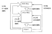
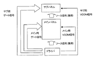
以下に本発明の実施例を図面に基づいて説明する。図1は本発明の表示装置のドライバと表示パネルの接続構成を示す概念図である。図2はメインパネルとサブパネルに印加する信号波形を示す図である。図3はモジュール構成を示す側面図である。 Embodiments of the present invention will be described below with reference to the drawings. FIG. 1 is a conceptual diagram showing a connection configuration between a driver and a display panel of a display device of the present invention. FIG. 2 is a diagram showing signal waveforms applied to the main panel and the sub panel. FIG. 3 is a side view showing the module configuration.
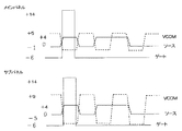
メインパネル1は128(RGB)×160ドットの画素構成である。表示のモードは透過型でポジ表示ある。サブパネル2は96(RGB)×64ドットの画素構成である。表示のモードは半透過型液晶でポジ表示である。ドライバIC4からは、ソース信号とゲート信号とメイン用VCOM信号とサブ用VCOM信号が出力されている。ソース信号とゲート信号はメインパネル1とサブパネル2で兼用している。メインパネル1とサブパネル2は画面サイズが違うため、サブパネル2には一部分の信号を接続している。ゲート信号で選択し、ソース信号の電圧レベルを素子の容量に保持する。このときゲート信号は14Vである。メインパネル1のVCOM信号は、+5Vと−1Vの矩形波である。ゲート信号のタイミングのVCOM信号に対して、ソース信号には電圧レベルが表示ONレベルと表示OFFレベルが変る。例えば、VCOM信号が+5Vの場合、ソース信号が0Vで電位差が5Vとなり表示はONに、+4Vでは電位差が1Vとなり表示はOFFとなる。また、VCOM信号が−1Vの場合、ソース信号が+4Vでは電位差5Vとなり、表示はONに、ソース信号が0Vでは電位差+1Vとなり表示はOFFとなる。このとき、サブパネル2側ではVCOM信号が+9Vと−5Vの矩形波である。
The main panel 1 has a pixel configuration of 128 (RGB) × 160 dots. The display mode is transmissive and positive display. The
サブパネル2に印加されるゲート信号とソース信号はメインパネル1と同一である。サブパネル2のVCOM信号が+9Vの場合、ソース信号が+4Vで電位差+5Vで、ソース信号が0Vで+9Vとなり、表示ONとなる。サブパネル2のVCOM信号が−5Vの場合ソース信号が+4Vで電位差+9Vで表示ON、ソース信号が0Vで電位差が+5Vで表示ONとなり、サブパネル2は全ての画素でON表示となり実質表示として黒画面となる。
The gate signal and source signal applied to the
サブパネル2を表示する場合は、サブのVCOM信号が+5Vと−1Vの電圧の矩形波とすることで、通常の表示ができる。このとき、携帯電話では閉じた状態であるため、メインパネル1は表示が見えない。VCOM信号を+2Vとすることで、液晶にかかる電位差が+2Vとなり低消費電力にすることができる。モジュールの構造としては、メインパネル1にドライバIC4を接続したFPC5を接続する。サブパネル2に必要な信号をFPC3によりメインパネル1と接続した構造である。
When the
上述の各構成では、ゲート信号とソース信号を兼用してメインパネル1を表示したままサブパネル2を全黒表示にすることができる。あるいは、偏光板の設定による光学設計により、ネガ表示とし、全白表示にすることもできる。また、サブパネル2のVCOM信号は液晶が全てのソース信号に対してON状態になるように設定したが、全てのソース信号に対してOFF状態になるようにしてもよい。
In each of the above-described configurations, the
また、メインパネル1とサブパネル2で異なる液晶材料を使用することにより、サブパネルのON表示の黒レベルを更に安定することができる。具体的にはメインパネル1よりサブパネル2に液晶急峻性の高い液晶を使用する。サブパネル2に使用する液晶は低電圧液晶がより望ましい。
Further, by using different liquid crystal materials for the main panel 1 and the
ドライバICは、従来のメインパネル用ドライバICにサブパネル用VCOM信号端子のみを追加するだけで両面表示用ドライバICにすることができる。そのため、チップサイズはほぼ従来のメインパネル用ドライバICと同サイズとなる。 The driver IC can be a double-sided display driver IC by adding only the sub-panel VCOM signal terminal to the conventional main panel driver IC. Therefore, the chip size is almost the same as that of a conventional main panel driver IC.
1 メインパネル
2 サブパネル
3 FPC
4 ドライバIC
5 FPC
1
4 Driver IC
5 FPC
Claims (6)
前記第一の表示パネルと前記第二の表示パネルを駆動する信号は、ゲート信号とソース信号とVCOM信号を含み、
前記第一の表示パネルと前記第二の表示パネルには同一のゲート信号とソース信号が供給され、
前記第一の表示パネルと前記第二の表示パネルにはそれぞれ独立してVCOM信号が供給されることを特徴とする表示装置。 A first display panel and a second display panel including active elements, and a driver IC for driving the first display panel and the second display panel,
The signals for driving the first display panel and the second display panel include a gate signal, a source signal, and a VCOM signal.
The same gate signal and source signal are supplied to the first display panel and the second display panel,
A display device, wherein a VCOM signal is independently supplied to each of the first display panel and the second display panel.
前記第一の表示パネルと前記第二の表示パネルを駆動するゲート信号及びソース信号を出力し、
前記第一の表示パネルには第一のVCOM信号を、前記第二の表示パネルには第二のVCOM信号をそれぞれ独立して供給することを特徴とする表示パネルのドライバIC。 A driver IC for driving the first display panel and the second display panel including active elements,
Outputting a gate signal and a source signal for driving the first display panel and the second display panel;
A display panel driver IC, wherein a first VCOM signal is supplied to the first display panel and a second VCOM signal is supplied to the second display panel independently.
Priority Applications (1)
| Application Number | Priority Date | Filing Date | Title |
|---|---|---|---|
| JP2004105354A JP2005292341A (en) | 2004-03-31 | 2004-03-31 | Display device and driver ic for display panel |
Applications Claiming Priority (1)
| Application Number | Priority Date | Filing Date | Title |
|---|---|---|---|
| JP2004105354A JP2005292341A (en) | 2004-03-31 | 2004-03-31 | Display device and driver ic for display panel |
Publications (1)
| Publication Number | Publication Date |
|---|---|
| JP2005292341A true JP2005292341A (en) | 2005-10-20 |
Family
ID=35325353
Family Applications (1)
| Application Number | Title | Priority Date | Filing Date |
|---|---|---|---|
| JP2004105354A Pending JP2005292341A (en) | 2004-03-31 | 2004-03-31 | Display device and driver ic for display panel |
Country Status (1)
| Country | Link |
|---|---|
| JP (1) | JP2005292341A (en) |
-
2004
- 2004-03-31 JP JP2004105354A patent/JP2005292341A/en active Pending
Similar Documents
| Publication | Publication Date | Title |
|---|---|---|
| US7167141B2 (en) | Liquid crystal display device | |
| US10741139B2 (en) | Goa circuit | |
| CN102967974B (en) | A kind of array base palte, display device and refreshing frequency control method | |
| US8242997B2 (en) | Liquid crystal display panel and liquid crystal display device having the same | |
| US20080252577A1 (en) | Liquid crystal display device having drive circuit | |
| CN101441377B (en) | Liquid crystal display device | |
| TWI286238B (en) | Driving method for liquid crystal display, liquid crystal display, and portable electronic machine | |
| CN1501345A (en) | display device | |
| US8054393B2 (en) | Liquid crystal display device | |
| JP2005222015A (en) | Flat display device | |
| US7646369B2 (en) | Method of driving liquid crystal display device, liquid crystal display device,and electronic apparatus | |
| JP2010102266A (en) | Liquid crystal display device and driving method therefor | |
| US8587506B2 (en) | Display device | |
| US10176779B2 (en) | Display apparatus | |
| US8264440B2 (en) | Display device, electronic apparatus and electronic system | |
| CN101471023A (en) | Driving system, electro-optic device, and electronic device | |
| JP4630410B2 (en) | Liquid crystal display device | |
| JP2008102242A (en) | Electro-optical device, drive circuit, and electronic device | |
| US20080122775A1 (en) | Display apparatus | |
| US20070171178A1 (en) | Active matrix display device | |
| US20060262063A1 (en) | Display device | |
| JP2005292341A (en) | Display device and driver ic for display panel | |
| JP4779165B2 (en) | Gate driver | |
| JP2005024979A (en) | Display device and driving method thereof | |
| JP2002072981A (en) | Liquid crystal display device |