JP3853473B2 - Thermal head drive device - Google Patents
Thermal head drive device Download PDFInfo
- Publication number
- JP3853473B2 JP3853473B2 JP19027297A JP19027297A JP3853473B2 JP 3853473 B2 JP3853473 B2 JP 3853473B2 JP 19027297 A JP19027297 A JP 19027297A JP 19027297 A JP19027297 A JP 19027297A JP 3853473 B2 JP3853473 B2 JP 3853473B2
- Authority
- JP
- Japan
- Prior art keywords
- resistance
- thermal head
- resistance value
- voltage
- heating
- Prior art date
- Legal status (The legal status is an assumption and is not a legal conclusion. Google has not performed a legal analysis and makes no representation as to the accuracy of the status listed.)
- Expired - Lifetime
Links
Images


Description
【0001】
【発明の属する技術分野】
本発明は、サーマルヘッド駆動装置に関し、詳細には、熱転写記録方式若しくは感熱記録方式を用いたプリンタ、ファクシミリ、複写機等に使用し得るサーマルヘッド駆動装置に関する。
【0002】
【従来の技術】
サーマルヘッドは、発熱抵抗素子を等間隔でライン上に形成し、発熱抵抗素子により発生するジュール熱を用いて記録を行うものである。サーマルヘッドによる記録は、感熱記録方式と熱転写方式に大別されるが、構造が簡単で、保守性・操作性に優れ、騒音がなく、また、安価で信頼性が高いといった多くの特長をもっている。そして、記録もモノクロからカラーまでできるため、用途が拡大してきており、このため、ファクシミリ、券売機、パソコン、ビデオ、電子黒板、OA関連機器の記録、各種のプリンタなどに広く使用されている。
【0003】
例えば、このサーマルヘッドを使用して、昇華プリンタ等の階調記録が可能なプリンタでは、サーマルヘッドの発熱抵抗素子のサーマルヘッド内での抵抗値のばらつきは印字エネルギーの差となって現れ、印字画像に濃度ムラが発生してしまう。このため、各発熱抵抗素子の抵抗値を基に印字データを演算し、均一なエネルギーで印字するためには抵抗値の補正が必要である。また、発熱抵抗素子は、経時的に抵抗値が変化する事が知られており、プリンタ電源投入時などに全発熱抵抗素子の抵抗値を測定し、この測定した抵抗値を用いて抵抗値の補正演算などを行うことが望ましい。
【0004】
つぎに、従来提案されている発熱抵抗素子の抵抗値のばらつきの補正方法を、具体例を挙げて説明する。例えば、特開昭60−244564号公報に記載されたサーマルプリンタが公知である。図10は、上記特開昭60−244564号公報に記載されたサーマルプリンタの構成を示すブロック図である。
【0005】
かかるサーマルプリンタは、図10に示す如く、サーマルヘッド200と、非印字用抵抗体201の抵抗値を測定する抵抗測定回路204と、印字用発熱抵抗体202に印加する電圧を発生する電圧発生回路205と、抵抗値測定回路204の抵抗値に基づいて、電圧発生回路205の出力電圧を制御する電圧制御回路206と、印字用発熱抵抗体202を選択的に駆動するための駆動パルス発生回路207と、サーマルヘッド200の印字用発熱抵抗体202および非印字用抵抗体201と外部回路とを着脱自在に接続するコネクタ203と、を備えている。
【0006】
上記の如く構成されるサーマルプリンタでは、サーマルヘッド200をサーマルプリンタに取り付けることにより、非印字用抵抗体201の両端には、コネクタ203を介して、抵抗測定回路204が接続され、印字用発熱抵抗体202の共通電極にはコネクタ203を介して電圧発生回路205の出力端子が接続され、印字用発熱抵抗体202の個別電極には、コネクタ203を介して駆動回路が接続されることになる。
【0007】
そして、非印字用抵抗体201の抵抗値が抵抗測定回路204で自動的に測定され、該抵抗測定回路204の測定値に基づいて、電圧制御回路206は電圧発生回路205の出力電圧を印字濃度に応じて予め設定されている最適値になるように制御している。すなわち、上記サーマルプリンタは、非印字用抵抗体201をサーマルヘッド200に付加し、この非印字用抵抗体201の抵抗値を測定し、印字用発熱抵抗体202の平均抵抗を推定するものである。
【0008】
しかるに、上記特開昭60−244564号公報に開示されたサーマルプリンタは、サーマルヘッドに非印字用抵抗体を設け、この非印字用抵抗体の抵抗値を測定して、印字用発熱素子の平均抵抗値を推定する構成であるので、専用のサーマルヘッドが必要となるとともに、抵抗値の測定精度が悪いという問題がある。
【0009】
また、特開昭60−244565号公報に記載れたサーマルプリンタが公知である。図11は、上記特開昭60−244565号公報に記載されたサーマルプリンタの構成を示すブロック図である。
【0010】
かかるサーマルプリンタは、図11に示す如く、サーマルヘッド301と、発熱抵抗体302の発熱抵抗を測定する抵抗測定回路304と、発熱抵抗体302に印加する電圧を発生する電圧発生回路305と、抵抗値測定回路304の抵抗値に基づいて、電圧発生回路305の出力電圧を制御する電圧制御回路306と、発熱抵抗体302を選択的に駆動するための駆動パルス発生回路307と、サーマルヘッド301の発熱抵抗体302と外部回路とを着脱自在に接続するコネクタ303と、検出用抵抗308とを備えている。
【0011】
上記の如く構成されるサーマルプリンタでは、サーマルヘッド301をサーマルサプリンタに取り付けることにより、発熱抵抗体302の共通電極にはコネクタ303および検出用抵抗308を介して電圧発生回路305の出力端子が接続されるとと共に、抵抗測定回路304および電圧制御回路306が接続され、発熱抵抗体302の個別電極にはコネクタ303を介して駆動回路が接続されることとなる。
【0012】
そして、電源投時に駆動パルス発生回路307から全ての発熱抵抗体302を同時に駆動するための駆動パルスを送出すると共に、検出用抵抗308の両端の電圧を抵抗測定回路304で測定することによって発熱抵抗体302群の抵抗値を求め、該抵抗測定回路304の測定値に基づいて、電圧制御回路306が電圧発生回路305の出力電圧を印字濃度に応じて予め定めた最適値になるように設定する。すなわち、上記サーマルプリンタは、サーマルヘッド電源経路に検出用抵抗308を挿入し、この検出用抵抗308の両端の電圧をA/D変換してサーマルヘッド301の発熱抵抗素子の抵抗を測定するものである。
【0013】
しかるに、特開昭60−244565は、サーマルヘッドを全素子がONとなるように駆動し、サーマルヘッドの印字電源ラインに挿入した抵抗の両端の電圧を検出して平均抵抗値を求める構成であるので、個々の発熱素子の抵抗値が解からないため、2値画像程度用にしか使えないという問題がある。
【0014】
これを解決する方法として、例えば、特開昭61−228970公報で開示されたサーマルヘッド駆動装置が公知である。図12は、上記特開昭60−244565号公報に記載されたサーマルプリンタの構成を示すブロック図である。
【0015】
かかるサーマルヘッド駆動装置は、図12に示す如く、サーマルヘッド上に形成された発熱抵抗体401と、発熱抵抗体401の各単位発熱抵抗体の電気抵抗値を測定する電気抵抗測定部(付図示)と、この電気抵抗に応じた印字パルスの印加時間を求めてこれに対応する印字制御データをメモリ404に格納するデータ処理部(不図示)と、各単位発熱体に対して印字制御データに対応する制御パルスを供給する印字制御部(不図示)と、を備えている。
【0016】
すなわち、かかるサーマルヘッド駆動装置は、サーマルヘッドに1画素のみがONとなるデータを転送し、印字を順次行うことで、印字用電源ラインに挿入した抵抗の両端に発生する電圧をA/D変換し、メモリに記憶していく事で、全発熱素子の抵抗値を各々測定するものである。
【0017】
【発明が解決しようとする課題】
しかしながら、特開昭61−228970公報で開示されたサーマルヘッド駆動装置では、以下の如き問題がある。この問題を、図13および図14を参照しつつ説明する。
【0018】
図13は、特開昭61−228970の1素子測定時の等価回路を示している。図13において、電源電圧をVH 、被測定素子(発熱抵抗体401)の抵抗値をRX 、抵抗測定用抵抗の抵抗値をR、A/D変換器の入力電圧をVR とすると、A/D変換器の入力電圧VR は、下式(1)により導出される。
【0019】
VR =(VH ・R)/(R+RX )・・・(1)
【0020】
図14は、図13の被測定素子の抵抗値RX とA/D変換器の入力電圧VR との関係を示す特性図である。図14に示す如く、被測定素子の抵抗値RX に対するA/D変換器の入力電圧VR は、抵抗測定用抵抗の抵抗値Rの影響により線形とはならず、被測定素子の抵抗値の測定に誤差が生じ、測定精度が悪いという問題がある。
【0021】
上記課題に鑑み、本発明の目的は、サーマルヘッドを構成する複数の発熱抵抗素子の各抵抗値を精度良く測定可能なサーマルヘッド駆動装置を提供することにある。
【0022】
また、本発明の目的は、サーマルヘッドを構成する複数の発熱抵抗素子の各々の抵抗値を精度良く測定可能で、かつ、印字モードと抵抗値測定モードとを実行可能なサーマルヘッド駆動装置を提供することにある。
【0023】
また、本発明の目的は、サーマルヘッドを構成する複数の発熱抵抗素子の各抵抗値を精度良く測定可能で、かつ、印字モードと抵抗値測定モードとで電源供給源を容易に切り替え可能なサーマルヘッド駆動装置を提供することにある。
【0024】
また、本発明の目的は、サーマルヘッドを構成する複数の発熱抵抗素子の各抵抗値を精度良く測定可能で、かつ、印字モードと抵抗値測定モードとで電源供給源を切り替える場合に、抵抗測定回路を破損させないサーマルヘッド駆動装置を提供することにある。
【0025】
また、本発明の目的は、サーマルヘッドを構成する複数の発熱抵抗素子の各抵抗値を精度良く測定可能で、かつ、簡単な構成で、抵抗測定回路を実現可能なサーマルヘッド駆動装置を提供することにある。
【0026】
また、本発明の目的は、サーマルヘッドを構成する複数の発熱抵抗素子の各抵抗値を精度良く測定可能で、かつ、抵抗値測定回路を構成するA/D変換器に適正レベルの電圧を入力可能なサーマルヘッド駆動装置を提供することにある。
【0027】
また、本発明の目的は、サーマルヘッドを構成する複数の発熱抵抗素子の各抵抗値を精度良く測定可能で、かつ、抵抗値測定回路を構成する増幅回路のゲインとオフセットを容易に調整可能なサーマルヘッド駆動装置を提供することにある。
【0028】
また、本発明の目的は、サーマルヘッドを構成する複数の発熱抵抗素子の各抵抗値を精度良く測定可能で、かつ、高速な抵抗値測定が可能なサーマルヘッド駆動装置を提供することにある。
【0029】
また、本発明の目的は、サーマルヘッドを構成する複数の発熱抵抗素子の各抵抗値を精度良く測定可能で、かつ、発熱抵抗素子の抵抗値がばらついても濃度ムラのない高画質の印字が可能なサーマルヘッド駆動装置を提供することにある。
【0030】
【課題を解決するための手段】
上記課題を解決するために、本発明に係るサーマルヘッド駆動装置は、サーマルヘッドを構成する複数の発熱抵抗素子を駆動して印字を行うサーマルヘッド駆動装置において、前記複数の発熱抵抗素子の抵抗値を測定するために、当該複数の発熱抵抗素子が接続される電源ラインに定電流を供給する定電流発生手段と、前記複数の発熱抵抗素子の各抵抗値を測定する抵抗値測定手段と、を備えたものである。
【0031】
すなわち、本発明に係るサーマルヘッド駆動装置によれば、複数の発熱抵抗素子の抵抗値を測定するために、複数の発熱抵抗素子が接続される電源ラインに定電流発生手段により定電流を供給して、複数の発熱抵抗素子の各抵抗値を測定することとしたので、抵抗測定用抵抗が不要となるため、この抵抗測定用抵抗による誤差がなくなり、精度良く複数の発熱抵抗素子の各抵抗値を測定することが可能となる。
【0032】
また、本発明に係るサーマルヘッド駆動装置は、サーマルヘッドを構成する複数の発熱抵抗素子を駆動して印字を行うサーマルヘッド駆動装置において、通常の印字を行う印字モードと、前記複数の発熱抵抗素子の抵抗値を測定する抵抗値測定モードとを有し、前記複数の発熱抵抗素子の抵抗値を測定するために、当該複数の発熱抵抗素子が接続される電源ラインに定電流を供給する定電流発生手段と、前記複数の発熱抵抗素子の各抵抗値を測定する抵抗値測定手段と、を備えたものである。
【0033】
すなわち、本発明に係るサーマルヘッド駆動装置によれば、印字モードと印刷モードを有し、複数の発熱抵抗素子の抵抗値を測定するために、複数の発熱抵抗素子が接続される電源ラインに定電流発生手段により定電流を供給して、複数の発熱抵抗素子の各抵抗値を測定することとしたので、印字モードと抵抗値測定モードとを実行可能となり、また、抵抗測定用抵抗が不要となるため、この抵抗測定用抵抗による誤差がなくなり、精度良く複数の発熱抵抗素子の各抵抗値を測定することが可能となる。
【0034】
また、本発明に係るサーマルヘッド駆動装置は、前記印字モードの場合には、印字用電圧供給手段の出力を前記電源ラインに接続する一方、前記抵抗値測定モードの場合には、前記定電流発生手段の出力を当該電源ラインに接続する電源切換手段を備えたものである。
【0035】
すなわち、本発明に係るサーマルヘッド駆動装置によれば、電源切換手段により、印字モードの場合には、印字用電圧供給手段の出力を電源ラインに接続する一方、抵抗値測定モードの場合には、定電流発生手段の出力を電源ラインに接続する構成であるので、請求項2に係るサーマルヘッド駆動装置の発明の効果に加えて、印字モードと抵抗値測定モードにおいて、電源ラインに接続する電源を容易に切換ることが可能となる。
【0036】
また、本発明に係るサーマルヘッド駆動装置は、前記電源切換手段は、前記電源ラインに前記印字用電圧供給手段が接続されている場合には、前記抵抗測定手段を、当該印字用電圧供給手段から電気的に切断する機構を備えたものである。
【0037】
すなわち、本発明に係るサーマルヘッド駆動装置によれば、電源切換手段は、抵抗値測定手段を、印字用電圧供給手段から電気的に切断することとしたので、抵抗値測定手段に高電圧が印加されて、抵抗値測定手段が破壊されるのを防止することが可能となる。
【0038】
また、本発明に係るサーマルヘッド駆動装置は、前記電源切換手段は、抵抗値測定モードが設定された場合には、前記電源ラインの電荷の放電を行った後に、当該電源ラインに定電流発生手段の出力を接続するものである。
【0039】
すなわち、本発明に係るサーマルヘッド駆動装置によれば、電源切換手段は、抵抗値測定モードが設定された場合には、電源ラインの電荷の放電を行った後に、電源ラインに定電流発生手段の出力を接続することとしたので、電源ラインの電荷により抵抗値測定手段が破壊されるのを防止することが可能となる。
【0040】
また、本発明に係るサーマルヘッド駆動装置は、前記抵抗値測定手段は、前記定電流発生手段の出力が供給される前記電源ラインに接続された複数の発熱抵抗素子を1素子毎に、順次ONさせることにより各発熱抵抗素子の両端にそれぞれ生じる電圧を夫々増幅して出力する増幅手段と、前記増幅手段の各出力をA/D変換して得られる各電圧データを出力するA/D変換手段と、前記A/D変換手段から出力される各電圧データに基づいて、前記複数の発熱抵抗素子の各抵抗値を算出する抵抗値算出手段と、を備えたものである。
【0041】
すなわち、本発明に係るサーマルヘッド駆動装置によれば、抵抗値測定手段を、定電流発生手段の出力が供給される電源ラインに接続された複数の発熱抵抗素子を1素子毎に、順次ONさせることにより各発熱抵抗素子にそれぞれ生じる電圧を夫々増幅して出力する増幅手段と、増幅手段の各出力をA/D変換して得られる各電圧データを出力するA/D変換手段と、A/D変換手段から出力される各電圧データに基づいて、複数の発熱抵抗素子の各抵抗値を算出する抵抗値算出手段と、電圧データに基づいて、複数の発熱抵抗素子の各々の抵抗値を算出する抵抗値算出手段と、を備えた構成としたので、簡単な回路構成で抵抗値測定手段を実現することが可能となる。
【0042】
また、本発明に係るサーマルヘッド駆動装置は、前記増幅手段は、入力される前記被測定電圧を、前記A/D変換手段の適正入力範囲内のレベルに増幅するために、DCオフセットを可変に設定できるDCオフセットレベル可変手段と、ゲインを可変に設定できるゲイン可変手段とを備えたものである。
【0043】
すなわち、本発明に係るサーマルヘッド駆動装置によれば、増幅手段に入力される被測定電圧をA/D変換手段の適正入力範囲内のレベルに増幅するために、増幅手段を、DCオフセットを可変に設定できるDCオフセットレベル可変手段と、ゲインを可変に設定できるゲイン可変手段とで構成したので、A/D変換手段に適正レベルの電圧を入力可能となり、A/D変換誤差を低減することが可能となる。
【0044】
また、本発明に係るサーマルヘッド駆動装置は、前記DCオフセットレベル可変手段は、前記発熱抵抗素子の下限抵抗値に略等しい基準抵抗を前記増幅手段の入力端子と接地間に接続した場合に、出力が前記A/D変換手段の略入力下限電圧になるようにDCオフセット値を調整するDCオフセット調整手段を備え、前記ゲイン可変手段は、前記発熱抵抗素子の上限抵抗値に略等しい基準抵抗を前記増幅手段の入力端子と接地間に接続した場合に、出力が前記A/D変換手段の略入力上限電圧になるようにゲインを調整するゲイン調整手段を備えたものである。
【0045】
すなわち、本発明に係るサーマルヘッド駆動装置によれば、DCオフセットレベル調整手段が、発熱抵抗素子の下限抵抗値に略等しい基準抵抗を前記増幅手段の入力端子と接地間に接続した場合に、出力がA/D変換手段の略入力下限電圧になるようにDCオフセット値を調整する一方、ゲイン調整手段が、発熱抵抗素子の上限抵抗値に略等しい基準抵抗を増幅手段の入力端子と接地間に接続した場合に、出力がA/D変換手段の略入力上限電圧になるようにゲインを調整することとしたので、増幅手段のゲインとDCオフセット電圧を簡単に精度良く調整することが可能となる。
【0046】
また、本発明に係るサーマルヘッド駆動装置は、前記定電流発生手段の出力は、抵抗素子の一端に接続され、抵抗値測定時以外のときには、前記抵抗素子の他端をグランドに接続させるスイッチ機構を有するスイッチ手段を備えたものである。
【0047】
すなわち、本発明に係るサーマルヘッド駆動装置は、定電流発生手段の出力を抵抗素子の一端に接続し、抵抗値測定時以外のときには、抵抗素子の他端をグランドに接続させるスイッチ機構を有するスイッチ手段を備えているので、本発明に係るサーマルヘッド駆動装置の効果に加えて、抵抗測定時以外のときには、定電流発生手段の出力は抵抗素子を介してグランドに落ちることになり、抵抗値測定手段に規定範囲外の電圧が入力されるのを防止することができると共に、抵抗の非測定状態から測定状態への電圧変化量を少なくし、高速な抵抗値測定が可能となる。
【0048】
また、本発明に係るサーマルヘッド駆動装置は、前記抵抗素子は、前記複数の発熱抵抗素子の略平均抵抗値を有するものである。
【0049】
すなわち、本発明に係るサーマルヘッド駆動装置によれば、抵抗素子の抵抗値を複数の発熱抵抗素子の略平均抵抗値としたので、より高速な抵抗測定が可能となる。
【0050】
また、本発明に係るサーマルヘッド駆動装置は、前記抵抗値測定手段により測定された前記複数の発熱抵抗素子の各抵抗値に基づいて、前記サーマルヘッドの印字制御を行う印字制御手段を備えたものである。
【0051】
すなわち、本発明に係るサーマルヘッド駆動装置によれば、測定された複数の発熱抵抗素子の各抵抗値に基づいて、サーマルヘッドの印字制御を行うこととしたので、発熱抵抗素子の抵抗値がばらついても濃度ムラのない高画質の印字が可能となる。
【0052】
【発明の実施の形態】
以下に添付図面を参照して、本発明に係るサーマルヘッド駆動装置の好適な実施の形態を詳細に説明する。
【0053】
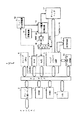
図1は、本発明に係るサーマルヘッド駆動装置を適用した熱記録装置の回路構成を示すブロック図である。
【0054】
図1において、1は熱記録装置を示しており、この熱記録装置1は、ホストコンピュータから送出される印字データを格納するスレーブ共有メモリ2と、スレーブCPU6が実行する制御プログラム(例えば、印字モード実行プログラムや抵抗測定モード実行プログラム等)を格納したROM3と、スレーブCPU6のワークメモリとして使用され各種データを格納するRAM4と、I/O5と、ROM3に格納された制御プログラムに基づいて装置内の各部の制御を司るスレーブCPU6と、D/A変換器7と、アンプAMP15からの出力をA/D変換するA/D変換器8と、を備えている。
【0055】
さらに、サーマルヘッド17を駆動するヘッドドライブ回路9と、スレーブ共有メモリ2から1ライン毎に転送される印字データを一時的に格納するデュアルポートRAM10と、ヘッドドライブ回路9(2値化部96)でレベル変換された印字データを格納する出力RAM11と、印字モードにおいてサーマルヘッド17に駆動電圧を供給するヘッド印字用電源12と、抵抗値測定モードにおいてサーマルヘッド17の発熱抵抗素子RX1〜RXnの抵抗値を測定するための定電流ICONSTをサーマルヘッド17の電源ライン(VHライン)に供給する定電流源13と、を備えている。
【0056】
さらに、動作モードに応じてヘッド印字用電源12と定電流源13との出力を択一的に切り替えてサーマルヘッド9に出力するヘッド電源切換回路14と、A/D変換器8に入力される電圧のレベルを調整するアンプAMP15と、A/D変換器8への入力を切り替えるアナログセレクタ16と、記録紙に熱定着を行うサーマルヘッド17とを備えている。
【0057】
上記構成の熱記録装置は、通常の印字を行う印字モードとサーマルヘッド17の発熱抵抗素子RX1〜RXnの抵抗値を測定する抵抗値測定モードとを備えており、上記スレーブCPU6は、これら印字モードおよび抵抗値測定モードを実行し、各動作モードの設定は、スレーブCPU6がヘッドドライブ回路9のモード設定レジスタ91にアクセスすることにより行われる。
【0058】
また、スレーブCPU6、A/D変換器8、およびアンプAMP15等は、抵抗測定回路を構成する。この抵抗測定回路は、抵抗値測定モードにおいて、サーマルヘッド17の発熱抵抗素子Rxの抵抗値を測定する。
【0059】
図2は、図1に示した定電流源13の具体的回路構成を示す図である。定電流源13は、図2に示す如く、ツェナーダイオードD1と、分圧抵抗RA、分圧抵抗RBと、アンプOP1と、およびトランジスタT1等を備えている。図2に示す如く、分圧抵抗RAと分圧抵抗RBは互いに直列接続されており、この直列回路には、ツェナーダイオードD1が並列接続されている。そして、この並列回路の一端は定電源(+VDD)に接続され、他端は抵抗R2を介して接地されている。
【0060】
また、アンプOP1の正相入力端子(+)は、分圧抵抗RAと分圧抵抗RBの分圧点に接続され、逆相入力端子(−)は、抵抗R1を介して定電源(+VDD)に接続されるとともに、トランジスタT1のドレインに接続され、アンプOP1の出力は、トランジスタT1のゲートに接続されている。そして、トランジスタT1のゲートは、アンプOP1の出力に接続され、そのドレインは、アンプの逆相入力端子(−)に接続されるとともに、抵抗R1を介して、定電源(+VDD)に接続され、そのソースはヘッド電源切換回路14に接続されている。
【0061】
上記構成の定電流源13においては、定電源から供給される電圧+VDDが、分圧抵抗RAと分圧抵抗RBとにより分圧されて、アンプOP1の正相入力端子(+)に供給され、また、電圧+VDDは、抵抗R1を介して、アンプOP1の逆相入力端子(−)に供給される。アンプOP1は、入力電圧を作動増幅した出力をトランジスタT1のゲートに供給して、トランジスタT1をスイッチングする。トランジスタT1は、アンプOP1の出力でスイッチングされて、定電源から抵抗R1を介して入力される電圧+VDDを増幅して得られる定電流ICONST を、ソースからヘッド電源切換回路14に出力する。
【0062】
すなわち、定電流源13においては、定電流ICONSTの大きさは、分圧抵抗RA と分圧抵抗RBにより決定される。従って、分圧抵抗RAと分圧抵抗RBの抵抗値を設定することにより、定電流ICONST の大きさを任意に設定することができる。
【0063】
図3は、図1のアンプAMP15の具体的回路構成を示す図である。アンプAMP15は、図3に示す如く、アンプAMP15のDCオフセット量を設定するDCオフセット可変部151と、定電流源13から供給される定電流ICONSTにより生じるサーマルヘッド17の発熱抵抗体VXの両端間の電圧を増幅してアナログセレクタ16に出力する増幅部152とから成る。アンプAMP15は、DCオフセット可変部151と増幅部152とにより、A/D変換器8に入力される発熱抵抗体VXの両端間の電圧VXのレベルをA/D変換器8の適正入力電圧範囲となるように調整している。
【0064】
上記DCオフセット可変部151は、アンプOP2や可変抵抗(DCオフセット調整ボリューム)VR1等からなり、可変抵抗VR1,分圧抵抗R4、および分圧抵抗R5からなる直列回路の一端は、抵抗R3を介して定電源+VCCに接続され、その他端は接地されている。この直列回路と抵抗R3間には、一端が接地されたツェナーダイオードD2が接続されている。
【0065】
そして、アンプOP2の正相入力端子(+)には、可変抵抗VR1が接続され、アンプOP2の出力はその逆相入力端子(−)に帰還されるとともに、抵抗R6を介して、増幅部152のアンプOP3の逆相入力端子(−)に接続されている。また、可変抵抗VR1とアンプOP2間には一端が接地されたコンデンサC1が接続され、アンプOP2と抵抗R6間には一端が接地されたコンデンサC2が接続されている。
【0066】
増幅部152は、アンプOP3や可変抵抗(ゲイン調整用ボリューム)VR2等からなり、アンプOP3の正相入力端子(+)には定電流源13からの出力が入力され、その逆相入力端子(−)は、DCオフセット可変部151のアンプOP2の出力に抵抗R6を介して接続される。アンプOP3の出力は、抵抗R8および可変抵抗VR2を介してアンプOP3の逆相入力端子(−)に帰還される一方、アナログセレクタ14を経てA/D変換器8に接続される。
【0067】
上記構成のアンプAMP15においては、先ず、DCオフセット可変部151において、定電源から供給される電圧+VCCが、可変抵抗VR1,分圧抵抗R4、および分圧抵抗R5からなる直列回路により分圧されて、アンプOP2の正相入力端子(+)に供給され、増幅された後、抵抗R6を介して、DCオフセット電圧としてアンプOP3の逆相入力端子(−)に出力される。増幅部152では、アンプOP3の正相入力端子(+)に入力される定電流源13から入力される電圧と逆相入力端子(−)に入力される電圧とを、抵抗R2と可変抵抗VR2で決定されるゲインで作動増幅して、アナログセレクタ16を介してA/D変換器8に出力する。
【0068】
すなわち、アンプAMP15では、DCオフセット電圧は、可変抵抗VR1により調整され、ゲインはVR2で調整される。従って、可変抵抗VR1を調整することによりDCオフセット電圧を所望値に設定し、可変抵抗VR2を調整することによりゲインを設定できる。
【0069】
つぎに、上記アンプAMP15のゲインとDCオフセット電圧の調整方法について説明する。前述のように、アンプAMP15を具備することにより、A/D変換器8のA/D変換誤差を小さくできるが、より好ましくは、ゲインとDCオフセット電圧を正確に調整する必要がある。
【0070】
ここで、サーマルヘッド17の発熱抵抗素子Rxの製造バラツキの下限値をRLow,上限値をRHigh、A/D変換器8の適正下限入力電圧をVLOW,上限入力電圧をVHIGHとする。
【0071】
先ず、増幅部152の入力INとグランド間に、RLowと略等しい基準抵抗を接続し、DCオフセット調整ボリューム(可変抵抗)VR1を、出力電圧OUTがVLOWとなるように調整する。つぎに、入力INとグランド間にRHighを接続し、ゲイン調整ボリューム(可変抵抗)VR2を、出力電圧OUTがVHIGHとなるように調整する。以上の操作を数回繰り返すことにより、ゲインとDCオフセット電圧は完全に調整され、入力INにRLowを接続した場合には出力電圧OUTがVLOW、入力INにRHighを接続した場合には出力電圧OUTがVHIGHとなる。これにより、サーマルヘッド17の発熱抵抗素子Rxで生じる電圧VXは、理想的な電圧範囲でA/D変換器8に入力され、高精度な抵抗値測定が可能となる。
【0072】
図4は、図1のサーマルヘッド17の詳細な回路構成例を示している。サーマルヘッド17は、図4に示す如く、ライン状に配置され、一端がVH ライン(電源ライン)に並列に接続され他端がスイッチング回路TR1〜TRnにそれぞれ接続された複数の発熱抵抗素子RX1〜RXnと、ヘッドドライブ回路9から入力されるシリアルの印字データDATAをパラレルのデータに変換するシフトレジスタ171と、シフトレジスタ171から出力されるパラレルのデータをヘッドドライブ回路9のタイミングコントローラ93(図5参照)から供給されるラッチパルス*LATCH(*はLOWアクティブを示す。以下、同様である)に基づいてラッチするラッチ回路172と、前記ラッチ回路172の出力線とストローブジェネレータ92(図5参照)から供給される発熱抵抗素子RX1〜RXnを駆動するためのストローブパルス*STB(*はLOWアクティブを示す。以下、同様である)の供給線とに接続され、ラッチ回路172のラッチ信号*LATCHとストローブパルス*STBとの論理積信号を出力するアンドゲートAND1〜ANDnと、アンドゲートAND1〜ANDnからの出力により開閉制御されて発熱抵抗素子RX1〜RXnに記録電流を流すスイッチング回路TR1〜TR2と、を備えている。
【0073】
また、上記VHラインには、一端が接地されたノイズ防止用コンデンサC(パスコン)が接続されている。なお、これらスイッチング回路TR1〜TRn、シフトレジスタ171、ラッチ回路172、およびアンドゲート173は、IC化されている。
【0074】
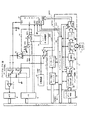
図5は、図1に示した熱記録装置の一部構成を示しており、特に、ヘッドドライブ回路9,ヘッド電圧切換回路14,およびアナログセレクタ16の詳細な構成並びにその周辺の構成を示すものである。
【0075】
上記ヘッドドライブ回路9は、図5に示す如く、動作モード(印刷モード、抵抗測定モード)やストローブ幅(DUTY)等の設定レジスタを備えたモード設定レジスタ91と、モード設定レジスタで設定されたストローブ幅(DUTY)のストローブパルス*STB(*はLOWアクティブを示す。以下、同様である)を発生してサーマルヘッド17に供給するストローブジェネレータ92と、内部システムクロック,ヘッドドライブ回路9内の各種タイミング信号,およびサーマルヘッド17を駆動するタイミング信号(クロックCKやラッチパルス*LATCH)を生成するタイミングコントローラ93と、デュアルポートRAM10のリード制御を行うデュアルポートRAMI/F94と、デュアルポートRAMI/F94の出力先を動作モードに応じて切り替えるSW95と、デュアルポートRAMI/F94から出力される階調データ(例えば、8bitのデータ)をサーマルヘッド17で印字可能な2値データに変換する2値化回路96と、2値化された印字データを出力RAM11にライトする出力RAMI/F97と、奇数画素と偶数画素を交互に印字するための印字データを出力するO−E(ODD−EVEN)フィルタ98と、動作モードに応じてサーマルヘッド17への印字データの出力を択一的に切り替えるSW99とから構成されている。
【0076】
ヘッド電圧切換回路14は、図5に示す如く、例えば、リレーRY1とリレーRY2とからなり、リレーRY1は、スレーブCPU6の制御により、ヘッド印字用電源14の+端子側に接続されたメーク接点(a1接点)側とリレーRY2を介して抵抗値測定回路に接続されるブレーク接点(b1接点)側との接続を切り替える。また、リレーRY2は、スレーブCPU6の制御により、抵抗値測定回路に接続されたメーク接点(a2接点)側と一端が接地された抵抗RSに接続されたブレーク接点(b2接点)側との接続を切り替える。この抵抗RSは、サーマルヘッド17のVH ラインに実装されているノイズ防止用コンデンサCに蓄積された電荷を放電するために設けられている。
【0077】
上記構成のヘッド電圧切換回路14においては、印字時には、リレーRY1をON(a1側に接続)とし、ヘッド印字用電源10の出力がサーマルヘッド17のVHライン(電源ライン)に印加される。リレーRY1がONしている場合は、抵抗値測定回路が接続されることはなく、ヘッド印字用電源12の高電圧が微少電圧用の抵抗値測定回路に入力されないため、抵抗値測定回路が破壊されるのを防止できる。
【0078】
非印字時のスタンバイ状態には、リレーRY1とリレーRY2が共にOFF(b1,b2側に接続)となっており、サーマルヘッド17のVHライン(電源ライン)と接地間に接続されたノイズ防止用コンデンサCの電荷は、抵抗RSから放電されるため、サーマルヘッド17の発熱抵抗素子RXに付着したナトリウムイオン等によるグランドへの不要放電による素子破壊を防止することができる。
【0079】
また、抵抗値測定時には、スレーブCPU6は、I/Oポート5を介して、先ずリレーRY1をOFFし、所定時間経過後、リレーRY2をONとする。これにより、定電流源13から定電流ICONSTがサーマルヘッド17のVH ラインに供給される。リレーRY1をOFFし、所定時間経過後、リレーRY2をONしているため、サーマルヘッド17のVHラインに実装されているノイズ防止用コンデンサC(図7参照)に蓄積された電荷を抵抗RSにより放電し、このコンデンサCに蓄積された電荷により抵抗値測定回路が破壊されるのを防止できる。また、抵抗値測定を行う場合は、リレーRY2をONしているため、抵抗RSはVHラインから切り離されることになり、抵抗RSは抵抗値測定には影響を与えない。
【0080】
アナログセレクタ16は、図5に示す如く、例えば、アナログスイッチSW1とアナログスイッチSW2からなり、アナログスイッチSW1は、スレーブCPU6の制御により、AMP15に接続されたX1側と、サーマルヘッド17のTHRに接続されたY1側との接続を切り替える。また、アナログスイッチSW2は、スレーブCPU6の制御により、無接続のX2側と、オープンコレクタTTL18を介してストローブジェネレータ92のストローブパルス*STB供給線に接続されるY2側との接続を切り替える。
【0081】
このY2側にはオープンコレクタTTL18がワイアードORで接続されている。このオープンコレクタTTL18は、ストローブジェネレータ92から出力されるストローブパルス*STBがアクティブでない時にONされる。また、このY2側とヘッド電圧切換回路14のリレーRY2のa2側間には、抵抗素子RTYPが接続されている。また、このa2側と抵抗素子RTYPの接続は、定電流源13とAMP15間の接続に交差している。かかる抵抗素子RTYPは、定電流源13の出力がアンプAMP15に入力されるのを防止するためのものである。
【0082】
上記構成のアナログセレクタ16においては、抵抗値測定時には、スレーブCPU6は、I/Oポート5を介して、アナログスイッチSW1をX1側に切り替えると共に、アナログスイッチSW2をX2側に切り替える。これにより、アンプAMP15の出力がSW1を経てA/D変換器8に入力され、抵抗値測定が行われる。また、アナログスイッチSW2は、X2側に接続されているため、抵抗素子RTYPは抵抗値測定には何ら影響を与えない。
【0083】
一方、サーマルヘッド17に搭載されたサーミスタと抵抗RTとで発生した電圧でサーマルヘッド17の温度を測定する場合には、スレーブCPU6は、I/Oポート5を介して、アナログスイッチSW1をY1側に切り替え、また、アナログスイッチSW2をY2側に切り替える。これにより、サーマルヘッド17のTHR出力は、アナログスイッチSW1とアンプを経てA/D変換器8に入力されることになる。また、アナログスイッチSW2は、Y2側へ接続されているため、定電流源13の出力は、抵抗素子RTYPを通じてGNDに落ちることになり、アンプAMP15には、定電流源13の出力を開放した高電圧が印加されることはない。
【0084】
上記図1〜図5の構成において、定電流源13は定電流発生手段を、抵抗測定回路は抵抗値測定手段を、ヘッド印字用電源12は印字用電源供給手段を、ヘッド電源切換回路14は電源切換手段を、アンプAMP15は増幅手段を、A/D変換器8はA/D変換手段を、スレーブCPU6は抵抗値算出手段および印字制御手段を、DCオフセット可変部151はDCオフセットレベル可変手段を、増幅部152はゲイン可変手段を、DCオフセット調整ボリュームVR1はDCオフセット調整手段を、ゲイン調整用ボリュームVR2はゲイン調整手段を、アナログセレクタ16はスイッチ手段を、それぞれ実現している。
【0085】
つぎに、上記熱記録装置の動作を説明する。上記図1〜図5の如く構成される熱記録装置1は、前述の如く、印刷モードと抵抗測定モードを有しており、以下、抵抗測定モード、印字モードの順に説明する。
【0086】
(抵抗測定モードの動作)
この抵抗測定モードは、サーマルヘッド17の全発熱抵抗素子RX1〜RXnの各抵抗値を測定するモードであり、定電流源13に接続されたサーマルヘッド17の発熱抵抗素子RX1〜RXnを1画素(1素子)ずつ順次ONし、発熱抵抗素子RXに生じる電圧VX(VH ラインとグランド間の電圧)をスレーブCPU6がA/D変換器8にA/D変換させ、このA/D変換された電圧データに基づいて発熱抵抗素子RXの抵抗値を算出する。この抵抗測定モードは、スレーブCPU6によりシステムの電源投入時等に実行される。
【0087】
図6は、抵抗値測定モードにおいて、発熱抵抗素子RX1(1素子)のみをONさせる場合のサーマルヘッド17およびその関連部(定電流源13,A/D変換器8)を模式的に示した図である。
【0088】
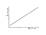
図7は、発熱抵抗素子RXの両端間に生じる電圧VXと、発熱抵抗素子RXとの関係を示す特性図である。
【0089】
図8は、抵抗値測定モードの動作を示すタイミングチャートであり、特に、オープンコレクタTTL18(図5参照)を作動させた場合のタイミングチャートを示している。
【0090】
図9は、抵抗値測定モードの動作を示すタイミングチャートであり、特に、オープンプンコレクタTTL18(図5参照)を作動させない場合のタイミングチャートを示している。
【0091】
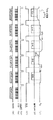
図8および図9において、(A)は、ヘッドドライブ回路9から出力されるデータDATAの波形を示しており、(B)は、タイミングコントローラ93から出力されるクロックCLKの波形を示しており、(C)は、タイミングコントローラ93から出力されるラッチパルス*LATCHの波形を示しており、(D)は、ストローブジェネレータ92から出力されるストローブパルス*STBの波形を示しており、(E)は、A/D変換器8の動作を示す波形を示しており、(F)は、VH ラインとグランド間の電圧VXの波形を示している。
【0092】
以下、上記図6〜図9を参照して、抵抗値測定モードの動作を説明する。スレーブCPU6は、電源投入後、所定の初期化終了後、ROM3に格納された抵抗値測定プログラムを実行する。先ず、スレーブCPU6は、ヘッドドライブ回路9のモード設定レジスタ91に対して、抵抗値測定モードの設定を行う。つぎに、スレーブCPU6は、I/Oポート5を介して、ヘッド電源切換回路14のリレーRY1をOFFしてb1側に接続するとともに、リレーRY2をONしてa2側に接続するとともに、アナログセレクタ16のアナログスイッチSW1およびSW2をX1、X2側にそれぞれ接続する。これにより、定電流源13の定電流ICONSTが、リレーRY1およびリレーRY2を経てサーマルヘッド17のVHラインに供給されることになる。
【0093】
つぎに、スレーブCPU6は、デュアルポートバッファRAM10にサーマルヘッド9の発熱抵抗素子Rxのうち最初の1素子Rx 1のみをONさせる1ライン分のデータDATA"100・・・00"を書き込み、タイミングコントローラ93に対してスタート指示を出す。
【0094】
これに応じて、ヘッドドライブ回路9では、デュアルポートRAMI/F94によりデュアルポートバッファRAM10から発熱抵抗素子RX1〜RXnの最初の1素子(RX1)のみをONさせる1ライン分の図8(A)の如きデータDATAを読み出すとともに、データスイッチSW95およびデータスイッチSW99をX側に接続して、印字モードで使用される2値化部96,出力RAMI/F97,およびO−Eフィルタ98をスルーして、サーマルヘッド17のシフトレジスタ171へ転送する。これと同時に、タイミングコントローラ19は、1ライン分の図8(B)の如きクロックCLKをサーマルヘッド17のシフトレジスタ171に転送する。
【0095】
続いて、タイミングコントローラ93は、図8(C)の如きラッチパルス*LATCHを、サーマルヘッド17のラッチ回路172に出力してラッチ回路172に転送データをラッチさせる。その後、ストローブジェネレータ92は、図7(D)に示す如く、ストローブパルス*STBを「LOW」にしてアクティブにするとともに、タイミングコントローラ93は、スレーブCPU6に対して割込信号LSYNCをアサートする。これに応じて、スレーブCPU6は、A/Dコンバータ8を起動する。
【0096】
かくして、図6に示す構成のサーマルヘッド171では、先ず、シフトレジスタ92が、転送される図8(B)の如きクロックCLKのタイミングで、転送される1ライン分の図8(A)の如きデータDATAを取り込んで、ラッチ回路172に順次出力する。
【0097】
この場合、図6に示す如く、シフトレジスタ92には、発熱抵抗素子RX1〜RXnの最初の1素子(Rx1)のみをONさせるデータ"100・・・000"が取り込まれることになる。ラッチ回路172は、図8(C)の如きラッチパルス*LATCHにより起動され、シフトレジスタから供給されるデータを取り込んで、アンドゲートAND1〜ANDnに順次出力する。この場合、図6に示す如く、発熱抵抗素子RX1〜RXnの最初の1素子(RX1)のみをONさせるデータがラッチされることになる。
【0098】
アンドゲートAND1〜ANDnでは、ラッチ回路172から供給されるデータと図8(D)の如きストローブ信号*STBがインバータにより反転された信号との論理積が演算され、得られる論理積信号が、スイッチング回路TR1〜TRnのベースに出力される。これにより、スイッチング回路TR1のみが動作して、トランジスタのコレクタに接続された発熱抵抗素子Tx1がONする。
【0099】
続いて、定電流源13から出力される定電流ICONST により、発熱抵抗素子TX1に生じる電圧VX1、すなわち、サーマルヘッド17のVHラインとGND間に生じる図8(F)の如き電圧VX1が、アンプAMP15、アナログスイッチSW16およびバッファを介してA/D変換器8に入力し、A/D変換器8は入力する電圧VX1を図8(E)に示すタイミングで、A/D変換して得られる電圧データをスレーブCPU6に出力する。スレーブCPU6は、入力される電圧データからR−Iの抵抗値を算出する。
【0100】
なお、スレーブCPU6は、抵抗値測定時でないときには、SW2をY2側に接続するとともに、ストローブパルス*STBがアクティブでない場合にオープンコレクタTTL18をONすることにより、高速な抵抗値測定を実現している。これについては、詳細は後述する。
【0101】
最初の1素子のA/D変換が終了したら、スレーブCPU6は、A/Dコンバータ8から入力される電圧データをRAM4に格納し、最初の素子の抵抗値測定を終了する。この動作をONさせる発熱抵抗素子を1素子ずつ順次移動して測定を全発熱抵抗素子の回数nだけ繰り返すことにより、サーマルヘッド17の全発熱抵抗素子RX1〜RXnの個々の電圧データをRAM4に格納する。
【0102】
ところで、アナログスイッチSW1がX2側に接続されている場合、すなわち、抵抗値測定時には、抵抗素子RTYPは開放状態であるが、サーマルヘッド17へのデータ転送時など、ストローブパルスSTBがアクティブでない時には、定電流源13の出力は、開放状態となり、開放電圧まで上昇してしまう。
【0103】
さらに、図6に示すように、サーマルヘッド17の電源ラインVHにはノイズ防止用コンデンサC(パスコン)が通常実装されているため、何も対策しないで抵抗測定を行うと、図9(F)に示す如く、一度定電流源の開放電圧まで跳ね上がった電圧はノイズ防止用コンデンサCに蓄積された電荷の放電により、ストローブパルス*STBをアクティブにしてもすぐにVX とはならず、だらだらと下降した後、VXに落ち着く。
【0104】
従って、スレーブCPU6は、ストローブパルス*STBをアクティブしてから一定時間ウエイトした後、A/D変換器8を起動しなければないため、高速な抵抗値測定が行えず、サーマルヘッド17の全発熱抵抗素子の抵抗値測定を行うのに非常に時間がかかってしまう。
【0105】
そこで、本実施の形態では、前述の抵抗値測定時以外の時、定電流源13の出力を抵抗素子RTYPを通じてGNDに落とすアナログスイッチSW2にワイアッドORでオープンコレクタTTL18を接続し、このオープンコレクタTTL18をストローブパルス*STBがアクティブでない時にはONするように構成することにより、図8(F)に示すように、ストローブパルス*STBがアクティブでない時も定電流源13の開放電圧まで跳ね上がる事がなくなり、これによってVx に安定するまでの時間が短くて済むため、高速な測定が可能となる。
【0106】
前述の抵抗素子RTYPの抵抗値をサーマルヘッド17の発熱抵抗素子RXの製造ばらつきの平均値とする事により、前述の効果をより大きくすることができ、より高速な抵抗値測定が可能となる。
【0107】
つぎに、上記抵抗値測定モードにおける抵抗測定方法を具体的に説明する。上記図7において、例えば、発熱抵抗素子RXの抵抗値RXVは、ドライブトランジスタT1のコレクタ−エミッタ間の飽和電圧をVCEとした場合、下式(2)の如く表すことができる。
【0108】
RXV=(VX −VCE)/(ICONST ) ・・(2)
【0109】
上記式(2)においては、ICONSTとVCEは一定となるため、抵抗値の測定精度は高くなる。また、スレーブCPU6は、電圧データの代わりに、上記式(2)で算出した抵抗値RXVを、RAM4に格納することにしても良い。
【0110】
つぎに、上記測定した抵抗値に基づいて、印字モードでの印字条件を決定する方法を具体的に説明する。
【0111】
実際の印字時の印字エネルギーEは、ヘッド印字電圧をVH、階調画像データをD、1階調当たりのストローブパルス幅をτとすると、データDを8ビット(0〜255)とした場合、下式(3)の如く表すことができる。
【0112】
E=(VH 2/RXV)・(D・255)・τ ・・・(3)
【0113】
スレーブCPU6は、上記式(3)の条件で、印字モードでサーマルヘッドを印字制御する事により、発熱抵抗素子RXの抵抗値RXVがばらついても、均一でムラのない画像を印字することができる。
【0114】
(印字モードの動作)
スレーブCPU6は、ROM6に格納された印字モード実行プログラムに基づいて、印字モードを実行する。先ず、スレーブCPU6は、ヘッドドライブ回路9に、印刷モードでスタート指示を出す。これにより、サーマルヘッドドライブ回路9は、フリーラン動作を開始する。続いて、スレーブCPU6は、デュアルポートRAM10に1ライン分の例えば8bitの階調データを書き込む。
【0115】
そして、デュアルポートRAMI/F94は、デュアルポートRAM10に書き込まれた1ライン分の階調データを読み出す。読み出された1ライン分の階調データは、SW95を介して、2値化回路96に出力される。2値化回路96は、階調データをサーマルヘッド17で印字可能な2値の256レベルデータに変換し、出力RAMI/F97は、この2値の256レベルデータを出力RAM11に書き込む。
【0116】
続いて、O−Eフィルタ98は、出力RAMI/F97により出力RAM11から読み出された第1レベルの2値データを、先ず、奇数画素有効、偶数画素を非印字データとして、サーマルヘッド17に転送する。この場合、タイミングコントローラ93は、転送クロックCLKを、同時にサーマルヘッド17のシフトレジスタ172に転送する。
【0117】
タイミングコントローラ93は、データ転送と転送クロックCLKの転送が完了すると、ラッチパルス*LATCHをサーマルヘッド17に転送し、続いて、タイミングコントローラ92が、サーマルヘッド17にラッチパルス*LATCHを送信する。これにより、サーマルヘッド17では奇数画素の印字が行われる。
【0118】
つぎに、出力RAMI/F97は、出力RAM11から同じ2値データを読み出し、奇数画素を非印字データ、偶数画素を有効としてサーマルヘッド17のシフトレジスタ173に転送する。タイミングコントローラ93は、同様に、転送クロックCLKを、同時にサーマルヘッド17のシフトレジスタ171に転送する。そして、タイミングコントローラ93は、データ転送と転送クロックCLKの転送が完了すると、続いて、サーマルヘッド17のラッチ回路172にラッチパルス*LATCHを送信する。これにより、サーマルヘッド17では偶数画素の印字が行われる。
【0119】
以上の処理を、第1レベルから第256レベルまで行い、1ラインの印字を終了すると、タイミングコントローラ93は、スレーブCPU6に対して、割り込み信号/LSYNCをアサートし、次ラインのデータ転送を要求する。
【0120】
以上説明したように、本実施の形態においては、サーマルヘッド17を構成する複数の発熱抵抗素子RX1〜RXnの抵抗値を測定するために、これら発熱抵抗素子RX1〜RXnが接続される電源ライン(VH ライン)に、定電流源13により定電流ICONSTを供給して、発熱抵抗素子RX1〜RXnの各抵抗値を測定することとしたので、抵抗測定用抵抗が不要となるため、この抵抗測定用抵抗による誤差がなくなり、精度良く複数の発熱抵抗素子の各抵抗値を測定することが可能となる。
【0121】
また、本実施の形態では、熱記録装置1は、印字モードと抵抗測定モードとを有しており、印字モードにおいては、スレーブCPU6は、1ライン周期の間に1ライン分の多値データをデュアルポートRAM10に書き込み、2値化部96でサーマルヘッド17で印字可能な2値データに変換し、出力RAM11,出力RAMI/F97、およびO−Eフィルタ98を介して、この2値化データをサーマルヘッド17に転送する構成である。
【0122】
他方、抵抗測定モードにおいては、スレーブCPU6は、1ライン周期の間に1ライン分の多値データをデュアルポートRAM10に書き込み、ヘッドドライブ回路9では、出力RAM11,出力RAMI/F97、およびO−Eフィルタ98をスルーしてこの多値データをサーマルヘッド17に転送する構成である。
【0123】
従って、印字モードと抵抗モードとでサーマルヘッド回路9の一部を共有して使用することができ、モード毎に、別々の回路を使用する場合に比して、回路規模を小さくできる。また、上記した如く、印字モードにおいては、スレーブCPU6が、デュアルポートRAM10に1ライン分の多値データを書き込むと、ヘッドドライブ回路9が、この多値データを2値レベルデータに変換して、階調数回、この2値レベルデータをサーマルヘッド17に転送する構成であるので、高速かつ高品質な階調印字を行う事が可能となる。
【0124】
また、本実施の形態においては、ヘッド電源切換回路15が、印字モードの場合には、ヘッド印字用電源14の出力をサーマルヘッド17の電源ライン(VHライン)に接続する一方、抵抗値測定モードの場合には、定電流源13の出力をサーマルヘッド17の電源ラインに接続する構成であるので、モードに応じて、電源ラインに接続する電源を容易に切換ることが可能となる。
【0125】
また、上記ヘッド電源切換回路15では、リレーRY1のメーク接点(a1接点)側にヘッド印刷用電源12が接続され、ブレーク接点(b1接点)側に抵抗値測定回路(アンプAMP15,A/D変換器8等)が接続される構成であるので、リレーRY1がON(a1側に接続)している場合には、抵抗値測定回路が接続されないため、ヘッド印字用電源12の高電圧が微少電圧用の抵抗値測定回路に入力されず抵抗値測定回路が破壊されるのを防止できる。
【0126】
また、上記ヘッド電源切換回路15は、抵抗値測定を行う場合に、スレーブCPU6の指示により、先ず、リレーRY1をOFF(b1側に接続)し、所定時間経過後、リレーRY2をON(a2側に接続)する構成であるので、サーマルヘッド17の電源ライン(VHライン)に実装されているノイズ防止用コンデンサCに蓄積された電荷を抵抗RSを介してグランドに放電でき、このノイズ防止用コンデンサCに蓄積された電荷により抵抗値測定回路が破壊されるのを防止できる。
【0127】
また、本実施の形態では、抵抗測定回路を、アンプAMP15、A/D変換器8、およびスレーブCPU6等で構築しているので、簡単な回路構成で抵抗値測定回路を実現することが可能となる。
【0128】
また、上記アンプAMP15を、DCオフセット電圧を可変に設定できるDCオフセット可変部151と、ゲインを可変に設定できる増幅部152とで構成したので、A/D変換器8に入力される電圧を、A/D変換器8の適正入力範囲内のレベルに増幅することができ、A/D変換器8に適正レベルの電圧が入力されA/D変換誤差を低減することが可能となる。
【0129】
付言すると、抵抗値測定時の発熱抵抗素子RX1〜RXnのストレスを少なくするため、できるだけ微少電流で抵抗を測定するのが望ましいが、微少電流では、発熱抵抗素子RX1〜RXnで発生する電圧が小さくなり、一般に、A/D変換誤差が大きくなる。本実施の形態では、アンプAMP15を上記構成としたので、微少電流で抵抗を測定する場合にも、A/D変換誤差を低減することが可能である。
【0130】
また、上記アンプAMP15のDCオフセット値を調整する場合に、発熱抵抗素子Rーの下限抵抗値に略等しい基準抵抗を、増幅部152の入力INと接地間に接続し、DCオフセット調整ボリュームVR1を調整して、出力がA/D変換器8の略入力下限電圧になるようにDCオフセット値を調整する構成である。
【0131】
また、上記AMP15のゲインを調整する場合に、発熱抵抗素子Rーの上限抵抗値に略等しい基準抵抗を増幅部152の入力端子INと接地間に接続し、ゲイン調整用ボリュームVR2を調整して、出力がA/D変換器8の略入力上限電圧になるようにゲインを調整する構成である。従って、AMP15のゲインとDCオフセット電圧を簡単に精度良く調整することが可能となる。
【0132】
また、本実施の形態では、定電流源13の出力を抵抗素子TTYPの一端に接続し、この抵抗素子TTYPの他端を、アナログセレクタ16のアナログSW2のY2側に接続し、また、このY2側に、ストローブジェネレータ92のストローブパルス*STB供給線に接続されたオープンコレクタTTL18をワイアードORで接続した構成において、抵抗値測定時以外の時、このアナログSW2をY2側に接続して、定電流源13の出力を抵抗素子RTYP を通じてGNDに落とすと共に、ストローブパルス*STBがアクティブでない場合には、オープンコレクタTTL16をONすることとした。
【0133】
これにより、抵抗値測定時以外のときには、定電流源13の出力は抵抗素子RTYPを介してグランドに落ちることになり、抵抗値測定回路に規定範囲外の電圧が入力されるのを防止することができると共に、抵抗の非測定状態から測定状態への電圧変化量を少なくすることができ、高速な抵抗値測定が可能となる。
【0134】
また、上記抵抗素子RTYP の抵抗値を発熱抵抗素子RX1〜RXnの略平均抵抗値としたので、より高速な抵抗測定が可能となる。
【0135】
また、本実施の形態においては、スレーブCPU6は、測定された複数の発熱抵抗素子RX1〜RXnの各抵抗値に基づいて、サーマルヘッドの印字制御を行うこととしたので、発熱抵抗素子RX1〜RXnの抵抗値がばらついても濃度ムラのない高画質の印字が可能となる。
【0136】
なお、上記した実施の形態では、本発明に係るサーマルヘッド駆動装置を熱記録装置に適用した場合を説明したが、本発明はこれに限られるものではなく、感熱記録装置等にも適用可能であることは勿論である。
【0137】
また、上記したタイミングチャートは、本発明に係るサーマルヘッド駆動装置を実現するための一例にすぎず、本発明に係るサーマルヘッド駆動装置を実現可能なタイミングであれば如何なるタイミングとしても良い。
【0138】
また、本発明は、上記実施の形態のみに限定されるものではなく、発明の要旨を変更しない範囲で適宜変形して実施可能である。
【0139】
【発明の効果】
以上説明したように、本発明によれば、複数の発熱抵抗素子の抵抗値を測定するために、複数の発熱抵抗素子が接続される電源ラインに定電流発生手段により定電流を供給して、複数の発熱抵抗素子の各抵抗値を測定することとしたので、抵抗測定用抵抗が不要となるため、この抵抗測定用抵抗による誤差がなくなり、精度良く複数の発熱抵抗素子の各抵抗値を測定することが可能となる。その結果、サーマルヘッドを構成する複数の発熱抵抗素子の各抵抗値を精度良く測定可能なサーマルヘッド駆動装置を提供することが可能となる。
【0140】
また、本発明によれば、印字モードと印刷モードを有し、複数の発熱抵抗素子の抵抗値を測定するために、複数の発熱抵抗素子が接続される電源ラインに定電流発生手段により定電流を供給して、複数の発熱抵抗素子の各抵抗値を測定することとしたので、印字モードと抵抗値測定モードとを実行可能となり、また、抵抗測定用抵抗が不要となるため、この抵抗測定用抵抗による誤差がなくなり、精度良く複数の発熱抵抗素子の各抵抗値を測定することが可能となる。この結果、サーマルヘッドを構成する複数の発熱抵抗素子の各々の抵抗値を精度良く測定可能で、かつ、印字モードと抵抗値測定モードとを実行可能なサーマルヘッド駆動装置を提供することが可能となる。
【0141】
また、本発明によれば、電源切換手段により、印字モードの場合には、印字用電圧供給手段の出力を電源ラインに接続する一方、抵抗値測定モードの場合には、定電流発生手段の出力を電源ラインに接続する構成であるので、印字モードと抵抗値測定モードにおいて、電源ラインに接続する電源を容易に切換ることが可能となる。その結果、サーマルヘッドを構成する複数の発熱抵抗素子の各抵抗値を精度良く測定可能で、かつ、印字モードと抵抗値測定モードとで電源供給源を容易に切り替え可能なサーマルヘッド駆動装置を提供することが可能となる。
【0142】
また、本発明によれば、電源切換手段は、印字モードにおいては、抵抗値測定手段を、印字用電圧供給手段から電気的に切断することとしたので、抵抗値測定手段に高電圧が印加されて、抵抗値測定手段が破壊されるのを防止することが可能となる。その結果、サーマルヘッドを構成する複数の発熱抵抗素子の各抵抗値を精度良く測定可能で、かつ、印字モードと抵抗値測定モードとで電源供給源を切り替えた場合に抵抗値測定精度を悪化させないサーマルヘッド駆動装置を提供することが可能となる。
【0143】
また、本発明によれば、電源切換手段は、抵抗値測定モードが設定された場合には、電源ラインの電荷の放電を行った後に、電源ラインに定電流発生手段の出力を接続することとしたので、電源ラインの電荷による抵抗値測定精度の悪化を防止することが可能となる。その結果、サーマルヘッドを構成する複数の発熱抵抗素子の各抵抗値を精度良く測定可能で、かつ、印字モードと抵抗値測定モードとで電源供給源を切り替えた場合に抵抗値測定精度を悪化させないサーマルヘッド駆動装置を提供することが可能となる。
【0144】
また、本発明によれば、抵抗値測定手段を、定電流発生手段の出力が供給される電源ラインに接続された複数の発熱抵抗素子を1素子毎に、順次ONさせることにより各発熱抵抗素子にそれぞれ生じる電圧を夫々増幅して出力する増幅手段と、増幅手段の各出力をA/D変換して得られる各電圧データを出力するA/D変換手段と、A/D変換手段から出力される各電圧データに基づいて、複数の発熱抵抗素子の各抵抗値を算出する抵抗値算出手段と、電圧データに基づいて、複数の発熱抵抗素子の各々の抵抗値を算出する抵抗値算出手段と、を備えた構成としたので、簡単な回路構成で抵抗値測定手段を実現することが可能となる。その結果、サーマルヘッドを構成する複数の発熱抵抗素子の各抵抗値を精度良く測定可能で、かつ、簡単な構成で、抵抗測定回路を実現可能なサーマルヘッド駆動装置を提供することが可能となる。
【0145】
また、本発明によれば、増幅手段に入力される被測定電圧をA/D変換手段の適正入力範囲内のレベルに増幅するために、増幅手段を、DCオフセットを可変に設定できるDCオフセットレベル可変手段と、ゲインを可変に設定できるゲイン可変手段とで構成したので、請求項6に係るサーマルヘッド駆動装置の効果に加えて、A/D変換手段に適正レベルの電圧を入力可能となり、A/D変換誤差を低減することが可能となる。その結果、サーマルヘッドを構成する複数の発熱抵抗素子の各抵抗値を精度良く測定可能で、かつ、抵抗値測定手段を構成するA/D変換手段に適正レベルの電圧を入力可能なサーマルヘッド駆動装置を提供することが可能となる。その結果、サーマルヘッドを構成する複数の発熱抵抗素子の各抵抗値を精度良く測定可能で、かつ、抵抗値測定回路を構成するA/D変換器に適正レベルの電圧を入力可能なサーマルヘッド駆動装置を提供することにある。
【0146】
また、本発明によれば、DCオフセットレベル調整手段が、発熱抵抗素子の下限抵抗値に略等しい基準抵抗を前記増幅手段の入力端子と接地間に接続した場合に、出力がA/D変換手段の略入力下限電圧になるようにDCオフセット値を調整する一方、ゲイン調整手段が、発熱抵抗素子の上限抵抗値に略等しい基準抵抗を増幅手段の入力端子と接地間に接続した場合に、出力がA/D変換手段の略入力上限電圧になるようにゲインを調整することとしたので、請求項7に係るサーマルヘッド駆動装置の効果に加えて、増幅手段のゲインとDCオフセット電圧を簡単に精度良く調整することが可能となる。その結果、サーマルヘッドを構成する複数の発熱抵抗素子の各抵抗値を精度良く測定可能で、かつ、抵抗値測定回路を構成する増幅回路のゲインとオフセットを容易に調整可能なサーマルヘッド駆動装置を提供することが可能となる。
【0147】
また、本発明によれば、定電流発生手段の出力を抵抗素子の一端に接続し、抵抗値測定時以外のときには、抵抗素子の他端をグランドに接続させるスイッチ機構を有するスイッチ手段を備えているので、抵抗測定時以外のときには、定電流発生手段の出力は抵抗素子を介してグランドに落ちることになり、抵抗値測定手段に規定範囲外の電圧が入力されるのを防止することができると共に、抵抗の非測定状態から測定状態への電圧変化量を少なくし、高速な抵抗値測定が可能となる。その結果、サーマルヘッドを構成する複数の発熱抵抗素子の各抵抗値を精度良く測定可能で、かつ、高速な抵抗値測定が可能なサーマルヘッド駆動装置を提供することが可能となる。
【0148】
また、本発明によれば、抵抗素子の抵抗値を複数の発熱抵抗素子の略平均抵抗値としたので、より高速な抵抗測定が可能となる。その結果、サーマルヘッドを構成する複数の発熱抵抗素子の各抵抗値を精度良く測定可能で、かつ、高速な抵抗値測定が可能なサーマルヘッド駆動装置を提供することが可能となる。
【0149】
また、本発明によれば、測定された複数の発熱抵抗素子の各抵抗値に基づいて、サーマルヘッドの印字制御を行うこととしたので、発熱抵抗素子の抵抗値がばらついても濃度ムラのない高画質の印字が可能となる。
【図面の簡単な説明】
【図1】 本発明に係るサーマルヘッド駆動装置を適用した熱記録装置の回路構成を示すブロック図である。
【図2】 図1に示した定電流源の具体的回路構成を示すブロック図である。
【図3】 図1に示したアンプの具体的回路構成を示すブロック図である。
【図4】 図1に示したサーマルヘッドの具体的な構成を示すブロック図である。
【図5】 図1に示した熱記録装置の一部構成を示す図である。
【図6】 抵抗値測定モードにおいて、発熱抵抗素子RX 1(1素子)のみをONさせる場合のサーマルヘッドおよびその関連部を模式的に示した図である。
【図7】 発熱抵抗素子RX の両端間に生じる電圧VX と、発熱抵抗素子RX との関係を示す特性図である。
【図8】 抵抗値測定モードの動作を示すタイミングチャートであり、特に、オープンコレクタTTL18を作動させた場合のタイミングチャートである。
【図9】 抵抗値測定モードの動作を示すタイミングチャートであり、特に、オープンプンコレクタTTL18を作動させない場合のタイミングチャートである。
【図10】 従来におけるサーマルプリンタの構成を示すブロック図である。
【図11】 従来におけるサーマルプリンタの構成を示すブロック図である。
【図12】 従来におけるサーマルヘッド駆動装置の構成を示すブロック図である。
【図13】 図12に示したサーマルヘッド駆動装置の1素子測定時の等価回路を示す説明図である。
【図14】 図13に示した被測定素子の抵抗値RXとA/D変換器の入力電圧VRとの関係を示す特性図である。
【符号の簡単な説明】
1 熱記録装置
2 スレーブ共有メモリ
3 ROM
4 RAM
5 I/O
6 スレーブCPU
7 D/A変換器
8 アナログ変換器
9 ヘッドドライブ回路
10 デュアルポートRAM
11 出力RAM
12 ヘッド印字用電源
13 定電流源
14 ヘッド電源切換回路
15 アンプAMP
16 アナログセレクタ
17 サーマルヘッド
18 オープンコレクタTTL
91 モード設定レジスタ
92 ストローブジェネレータ
93 タイミングコントローラ
94 デュアルポートRAMI/F
95 SW
96 2値化部
97 出力RAMI/F
98 O−Eフィルタ
99 SW
171 シフトレジスタ
172 ラッチ回路[0001]
BACKGROUND OF THE INVENTION
The present invention relates to a thermal head driving device, and more particularly to a thermal head driving device that can be used in a printer, a facsimile, a copying machine, or the like using a thermal transfer recording system or a thermal recording system.
[0002]
[Prior art]
In the thermal head, heating resistance elements are formed on a line at equal intervals, and recording is performed using Joule heat generated by the heating resistance elements. Thermal head recording is roughly divided into thermal recording and thermal transfer, but it has many features such as simple structure, excellent maintainability and operability, no noise, low cost and high reliability. . Since the recording can be performed from monochrome to color, the application has been expanded. For this reason, it is widely used for facsimiles, ticket vending machines, personal computers, videos, electronic blackboards, OA-related device recordings, various printers, and the like.
[0003]
For example, in a printer capable of gradation recording, such as a sublimation printer, using this thermal head, variations in the resistance value of the thermal head's heating resistance element within the thermal head appear as a difference in printing energy. Density unevenness occurs in the image. For this reason, it is necessary to correct the resistance value in order to calculate print data based on the resistance value of each heating resistance element and to print with uniform energy. In addition, it is known that the resistance value of the heating resistor element changes with time. The resistance value of all the heating resistor elements is measured when the printer power is turned on, and the resistance value is calculated using the measured resistance value. It is desirable to perform correction calculation.
[0004]
Next, a conventionally proposed method for correcting variation in resistance value of the heating resistor element will be described with a specific example. For example, a thermal printer described in JP-A-60-244564 is known. FIG. 10 is a block diagram showing the configuration of the thermal printer described in Japanese Patent Laid-Open No. 60-244564.
[0005]
As shown in FIG. 10, the thermal printer includes a
[0006]
In the thermal printer configured as described above, the
[0007]
Then, the resistance value of the
[0008]
However, the thermal printer disclosed in JP-A-60-244564 is provided with a non-printing resistor on the thermal head, and the resistance value of the non-printing resistor is measured to determine the average of the heating elements for printing. Since the resistance value is estimated, there is a problem that a dedicated thermal head is required and the measurement accuracy of the resistance value is poor.
[0009]
Also, a thermal printer described in JP-A-60-244565 is known. FIG. 11 is a block diagram showing the configuration of the thermal printer described in Japanese Patent Laid-Open No. 60-244565.
[0010]
As shown in FIG. 11, the thermal printer includes a
[0011]
In the thermal printer configured as described above, the output terminal of the
[0012]
Then, when the power is turned on, a driving pulse for driving all the
[0013]
However, Japanese Patent Laid-Open No. 60-244565 is a configuration in which the thermal head is driven so that all elements are turned on, and the voltage across the resistor inserted into the print power line of the thermal head is detected to obtain the average resistance value. Therefore, since the resistance value of each heating element is not known, there is a problem that it can be used only for binary images.
[0014]
As a method for solving this, for example, a thermal head driving device disclosed in Japanese Patent Laid-Open No. 61-228970 is known. FIG. 12 is a block diagram showing the configuration of the thermal printer described in Japanese Patent Laid-Open No. 60-244565.
[0015]
As shown in FIG. 12, the thermal head driving apparatus includes a
[0016]
That is, such a thermal head drive device A / D converts the voltage generated at both ends of the resistor inserted in the printing power supply line by transferring data in which only one pixel is turned on to the thermal head and performing printing sequentially. The resistance values of all the heating elements are measured by storing them in the memory.
[0017]
[Problems to be solved by the invention]
However, the thermal head driving device disclosed in Japanese Patent Laid-Open No. 61-228970 has the following problems. This problem will be described with reference to FIG. 13 and FIG.
[0018]
FIG. 13 shows an equivalent circuit at the time of measuring one element in Japanese Patent Laid-Open No. 61-228970. In FIG. 13, the power supply voltage is VHThe resistance value of the element to be measured (heating resistor 401) is RX, Resistance value of resistance for resistance measurement is R, input voltage of A / D converter is VRThen, the input voltage V of the A / D converterRIs derived by the following equation (1).
[0019]
VR= (VH・ R) / (R + RX) ... (1)
[0020]
FIG. 14 shows the resistance value R of the device under measurement of FIG.XAnd A / D converter input voltage VRIt is a characteristic view which shows the relationship. As shown in FIG. 14, the resistance value R of the element to be measuredXInput voltage V of A / D converter with respect toRIs not linear due to the influence of the resistance value R of the resistance measurement resistor, and there is a problem that an error occurs in the measurement of the resistance value of the element under measurement and the measurement accuracy is poor.
[0021]
In view of the above problems, an object of the present invention is to provide a thermal head driving device capable of accurately measuring each resistance value of a plurality of heating resistance elements constituting a thermal head.
[0022]
Another object of the present invention is to provide a thermal head driving device capable of measuring each resistance value of a plurality of heating resistance elements constituting a thermal head with high accuracy and capable of executing a print mode and a resistance value measurement mode. There is to do.
[0023]
Another object of the present invention is to provide a thermal head capable of measuring each resistance value of a plurality of heating resistance elements constituting a thermal head with high accuracy and easily switching a power supply source between a print mode and a resistance value measurement mode. It is to provide a head driving device.
[0024]
Another object of the present invention is to measure resistance when each resistance value of a plurality of heating resistance elements constituting a thermal head can be measured with high accuracy and when the power supply source is switched between the print mode and the resistance value measurement mode. It is an object of the present invention to provide a thermal head driving device that does not damage a circuit.
[0025]
Another object of the present invention is to provide a thermal head driving device capable of measuring each resistance value of a plurality of heating resistance elements constituting a thermal head with high accuracy and realizing a resistance measuring circuit with a simple configuration. There is.
[0026]
Another object of the present invention is to accurately measure each resistance value of a plurality of heating resistance elements constituting a thermal head and to input an appropriate level voltage to an A / D converter constituting the resistance value measurement circuit. It is an object of the present invention to provide a possible thermal head driving device.
[0027]
Another object of the present invention is to accurately measure the resistance values of a plurality of heating resistance elements constituting a thermal head and to easily adjust the gain and offset of an amplifier circuit constituting the resistance value measurement circuit. An object is to provide a thermal head driving device.
[0028]
Another object of the present invention is to provide a thermal head driving apparatus that can measure each resistance value of a plurality of heating resistance elements constituting a thermal head with high accuracy and can measure the resistance value at high speed.
[0029]
Another object of the present invention is to accurately measure each resistance value of a plurality of heating resistance elements constituting a thermal head, and to perform high-quality printing without density unevenness even if the resistance values of the heating resistance elements vary. It is an object of the present invention to provide a possible thermal head driving device.
[0030]
[Means for Solving the Problems]
In order to solve the above-described problems, a thermal head driving device according to the present invention is a thermal head driving device that performs printing by driving a plurality of heating resistance elements constituting a thermal head, and the resistance values of the plurality of heating resistance elements. A constant current generating means for supplying a constant current to a power supply line connected to the plurality of heating resistance elements, and a resistance value measuring means for measuring each resistance value of the plurality of heating resistance elements. It is provided.
[0031]
That is, according to the thermal head driving device of the present invention, in order to measure the resistance values of the plurality of heating resistance elements, a constant current is supplied to the power supply line to which the plurality of heating resistance elements are connected by the constant current generating means. Since each resistance value of a plurality of heating resistance elements is measured, resistance for resistance measurement is not required, so there is no error due to this resistance for resistance measurement, and each resistance value of the plurality of heating resistance elements is accurate. Can be measured.
[0032]
The thermal head driving device according to the present invention is a thermal head driving device that performs printing by driving a plurality of heating resistance elements constituting the thermal head, and a printing mode for performing normal printing, and the plurality of heating resistance elements. A resistance value measurement mode for measuring the resistance value of the plurality of heating resistance elements, and for measuring the resistance values of the plurality of heating resistance elements, a constant current for supplying a constant current to a power supply line to which the plurality of heating resistance elements are connected A generating means; and a resistance value measuring means for measuring each resistance value of the plurality of heating resistance elements.
[0033]
That is, according to the thermal head driving device of the present invention, the print mode and the print mode are provided. In order to measure the resistance values of the plurality of heating resistance elements, the power supply line connected to the plurality of heating resistance elements is fixed. Since a constant current is supplied by the current generating means and each resistance value of the plurality of heating resistance elements is measured, the print mode and the resistance value measurement mode can be executed, and a resistance measurement resistor is not required. Therefore, the error due to the resistance measurement resistor is eliminated, and each resistance value of the plurality of heating resistance elements can be measured with high accuracy.
[0034]
The thermal head driving device according to the present invention connects the output of the printing voltage supply means to the power line in the printing mode, while generating the constant current in the resistance measurement mode. Power supply switching means for connecting the output of the means to the power supply line.
[0035]
That is, according to the thermal head driving device of the present invention, the power switching means connects the output of the printing voltage supply means to the power line in the case of the printing mode, while in the resistance value measuring mode, Since the output of the constant current generating means is connected to the power supply line, in addition to the effect of the invention of the thermal head driving device according to
[0036]
Further, in the thermal head driving device according to the present invention, the power supply switching means is configured such that, when the printing voltage supply means is connected to the power supply line, the resistance measurement means is connected to the printing voltage supply means. A mechanism for electrically cutting is provided.
[0037]
That is, according to the thermal head driving device of the present invention, the power source switching means electrically disconnects the resistance value measuring means from the printing voltage supply means, so that a high voltage is applied to the resistance value measuring means. As a result, it is possible to prevent the resistance value measuring means from being destroyed.
[0038]
Further, in the thermal head driving device according to the present invention, the power source switching means, when the resistance value measurement mode is set, discharges the charge of the power source line, and then generates a constant current generating means for the power source line. Is connected to the output.
[0039]
That is, according to the thermal head driving device of the present invention, the power supply switching means, when the resistance value measurement mode is set, discharges the charge of the power supply line and then supplies the constant current generating means to the power supply line. Since the output is connected, it is possible to prevent the resistance value measuring means from being destroyed by the charge of the power supply line.
[0040]
In the thermal head driving device according to the present invention, the resistance value measuring means sequentially turns on a plurality of heating resistance elements connected to the power supply line to which the output of the constant current generating means is supplied, one by one. Amplifying means for amplifying and outputting the voltages generated at both ends of each heating resistor element, and A / D converting means for outputting each voltage data obtained by A / D converting each output of the amplifying means And resistance value calculating means for calculating the resistance values of the plurality of heating resistance elements based on the voltage data output from the A / D conversion means.
[0041]
That is, according to the thermal head driving device of the present invention, the resistance value measuring means sequentially turns on the plurality of heating resistance elements connected to the power supply line to which the output of the constant current generating means is supplied for each element. Amplifying means for amplifying and outputting the voltage generated in each heating resistor element, A / D conversion means for outputting each voltage data obtained by A / D converting each output of the amplifying means, A / Based on each voltage data output from the D conversion means, a resistance value calculating means for calculating each resistance value of the plurality of heating resistance elements, and calculating each resistance value of the plurality of heating resistance elements based on the voltage data Therefore, the resistance value measuring means can be realized with a simple circuit configuration.
[0042]
Further, in the thermal head driving apparatus according to the present invention, the amplifying means variably changes a DC offset in order to amplify the input voltage to be measured to a level within an appropriate input range of the A / D converting means. DC offset level variable means that can be set, and gain variable means that can variably set the gain.
[0043]
That is, according to the thermal head driving device of the present invention, the amplifying means is variable in DC offset in order to amplify the voltage to be measured input to the amplifying means to a level within the appropriate input range of the A / D converting means. Since the DC offset level variable means that can be set to the value and the gain variable means that can set the gain to be variable, a voltage of an appropriate level can be input to the A / D conversion means, and the A / D conversion error can be reduced. It becomes possible.
[0044]
In the thermal head driving device according to the present invention, the DC offset level varying means outputs an output when a reference resistance substantially equal to the lower limit resistance value of the heating resistance element is connected between the input terminal of the amplifying means and the ground. DC offset adjustment means for adjusting the DC offset value so that the value becomes substantially the input lower limit voltage of the A / D conversion means, and the gain variable means has a reference resistance substantially equal to the upper limit resistance value of the heating resistor element. When connected between the input terminal of the amplifying means and the ground, a gain adjusting means is provided for adjusting the gain so that the output becomes a substantially input upper limit voltage of the A / D converting means.
[0045]
That is, according to the thermal head driving device of the present invention, when the DC offset level adjusting means connects a reference resistance substantially equal to the lower limit resistance value of the heating resistance element between the input terminal of the amplifying means and the ground, the output While the DC offset value is adjusted so that becomes the approximate input lower limit voltage of the A / D conversion means, the gain adjustment means applies a reference resistance substantially equal to the upper limit resistance value of the heating resistance element between the input terminal of the amplification means and the ground. When the connection is made, the gain is adjusted so that the output becomes a substantially input upper limit voltage of the A / D conversion means. Therefore, the gain of the amplification means and the DC offset voltage can be easily and accurately adjusted. .
[0046]
In the thermal head driving device according to the present invention, the output of the constant current generating means is connected to one end of the resistance element, and the other end of the resistance element is connected to the ground when the resistance value is not measured. It is provided with the switch means which has.
[0047]
That is, the thermal head driving device according to the present invention has a switch mechanism that connects the output of the constant current generating means to one end of the resistance element, and connects the other end of the resistance element to the ground when the resistance value is not measured. In addition to the effects of the thermal head drive device according to the present invention, the output of the constant current generating means falls to the ground via the resistance element in addition to the effect of resistance measurement. The voltage outside the specified range can be prevented from being input to the means, and the amount of voltage change from the non-measurement state to the measurement state can be reduced, and high-speed resistance measurement can be performed.
[0048]
In the thermal head driving apparatus according to the present invention, the resistance element has a substantially average resistance value of the plurality of heating resistance elements.
[0049]
That is, according to the thermal head driving device of the present invention, the resistance value of the resistance element is set to the substantially average resistance value of the plurality of heating resistance elements, so that the resistance measurement can be performed at a higher speed.
[0050]
The thermal head driving device according to the present invention further comprises a print control means for performing print control of the thermal head based on the resistance values of the plurality of heating resistance elements measured by the resistance value measuring means. It is.
[0051]
That is, according to the thermal head driving device according to the present invention, since the thermal head printing control is performed based on the measured resistance values of the plurality of heating resistance elements, the resistance values of the heating resistance elements vary. However, high-quality printing without density unevenness is possible.
[0052]
DETAILED DESCRIPTION OF THE INVENTION
Exemplary embodiments of a thermal head driving apparatus according to the present invention will be explained below in detail with reference to the accompanying drawings.
[0053]
FIG. 1 is a block diagram showing a circuit configuration of a thermal recording apparatus to which a thermal head driving apparatus according to the present invention is applied.
[0054]
In FIG. 1,
[0055]
Further, a
[0056]
Further, the head power
[0057]
The thermal recording apparatus having the above configuration has a printing mode in which normal printing is performed and a heating resistance element R of the thermal head 17.X1-RXa resistance value measurement mode for measuring the resistance value of n, and the
[0058]
The
[0059]
FIG. 2 is a diagram showing a specific circuit configuration of the constant
[0060]
The positive phase input terminal (+) of the amplifier OP1 is connected to the voltage dividing resistor R.AAnd voltage dividing resistance RBThe negative phase input terminal (−) is connected to a constant power source (+ V) via a resistor R1.DD) And the drain of the transistor T1, and the output of the amplifier OP1 is connected to the gate of the transistor T1. The gate of the transistor T1 is connected to the output of the amplifier OP1, the drain thereof is connected to the negative phase input terminal (−) of the amplifier, and the constant power source (+ V) is connected via the resistor R1.DD) And its source is connected to the head power
[0061]
In the constant
[0062]
That is, in the constant
[0063]
FIG. 3 is a diagram showing a specific circuit configuration of the amplifier AMP15 of FIG. The amplifier AMP15 includes a DC offset variable unit 151 that sets a DC offset amount of the amplifier AMP15 and a constant current I supplied from the constant
[0064]
The DC offset variable unit 151 includes an amplifier OP2, a variable resistor (DC offset adjustment volume) VR1, and the like, and one end of a series circuit including the variable resistor VR1, the voltage dividing resistor R4, and the voltage dividing resistor R5 is connected via the resistor R3. Constant power supply + VCCThe other end is grounded. A Zener diode D2 having one end grounded is connected between the series circuit and the resistor R3.
[0065]
The variable resistor VR1 is connected to the positive phase input terminal (+) of the amplifier OP2, the output of the amplifier OP2 is fed back to the negative phase input terminal (−), and the amplifying unit 152 is connected via the resistor R6. Connected to the negative phase input terminal (−) of the amplifier OP3. Further, a capacitor C1 having one end grounded is connected between the variable resistor VR1 and the amplifier OP2, and a capacitor C2 having one end grounded is connected between the amplifier OP2 and the resistor R6.
[0066]
The amplification unit 152 includes an amplifier OP3, a variable resistor (gain adjustment volume) VR2, and the like. The output from the constant
[0067]
In the amplifier AMP15 having the above configuration, first, in the DC offset variable unit 151, the voltage + V supplied from the constant power source is set.CCIs divided by a series circuit including a variable resistor VR1, a voltage dividing resistor R4, and a voltage dividing resistor R5, supplied to the positive phase input terminal (+) of the amplifier OP2, amplified, and then passed through the resistor R6. , And output as a DC offset voltage to the negative phase input terminal (−) of the amplifier OP3. In the amplifying unit 152, the voltage inputted from the constant
[0068]
That is, in the amplifier AMP15, the DC offset voltage is adjusted by the variable resistor VR1, and the gain is adjusted by VR2. Therefore, the DC offset voltage can be set to a desired value by adjusting the variable resistor VR1, and the gain can be set by adjusting the variable resistor VR2.
[0069]
Next, a method for adjusting the gain and DC offset voltage of the amplifier AMP15 will be described. As described above, by providing the amplifier AMP15, the A / D conversion error of the A /
[0070]
Here, the heating resistance element R of the
[0071]
First, between the input IN of the amplifying unit 152 and the ground, RLowIs connected to a reference resistor substantially equal to the DC offset adjustment volume (variable resistor) VR1, and the output voltage OUT is VLOWAdjust so that Next, R between input IN and groundHighIs connected, gain adjustment volume (variable resistor) VR2, output voltage OUT is VHIGHAdjust so that By repeating the above operation several times, the gain and the DC offset voltage are completely adjusted, and the input IN has RLowOutput voltage OUT is VLOW, Input IN RHighOutput voltage OUT is VHIGHIt becomes. Thereby, the heating resistance element R of the
[0072]
FIG. 4 shows a detailed circuit configuration example of the
[0073]
In addition, the above VHA noise prevention capacitor C (pass capacitor) having one end grounded is connected to the line. These switching circuits TR1~ TRnThe
[0074]
FIG. 5 shows a partial configuration of the thermal recording apparatus shown in FIG. 1, and particularly shows the detailed configuration of the
[0075]
As shown in FIG. 5, the
[0076]
As shown in FIG. 5, the head
[0077]
In the head
[0078]
In the standby state during non-printing, both the relay RY1 and the relay RY2 are OFF (connected to the b1 and b2 sides), and the thermal head 17 VHThe charge of the noise prevention capacitor C connected between the line (power line) and the ground is the resistance RSThe heat generating resistive element R of the
[0079]
When measuring the resistance value, the
[0080]
As shown in FIG. 5, the
[0081]
An open collector TTL 18 is connected to the Y2 side by a wired OR. The open collector TTL 18 is turned on when the strobe pulse * STB output from the strobe generator 92 is not active. Further, there is a resistance element R between the Y2 side and the a2 side of the relay RY2 of the head voltage switching circuit 14.TYPIs connected. The a2 side and the resistance element RTYPIs crossing the connection between the constant
[0082]
In the
[0083]
On the other hand, the thermistor mounted on the
[0084]
1 to 5, the constant
[0085]
Next, the operation of the thermal recording apparatus will be described. The
[0086]
(Operation in resistance measurement mode)
In this resistance measurement mode, all the heating resistance elements R of the
[0087]
FIG. 6 shows the heating resistance element R in the resistance value measurement mode.XIt is the figure which showed typically the
[0088]
FIG. 7 shows a heating resistor element RXThe voltage V generated acrossXAnd heating resistance element RXIt is a characteristic view which shows the relationship.
[0089]
FIG. 8 is a timing chart showing an operation in the resistance value measurement mode, and particularly shows a timing chart when the open collector TTL 18 (see FIG. 5) is operated.
[0090]
FIG. 9 is a timing chart showing the operation in the resistance value measurement mode, and particularly shows a timing chart when the open-pump collector TTL 18 (see FIG. 5) is not operated.
[0091]
8 and 9, (A) shows the waveform of the data DATA output from the
[0092]
Hereinafter, the operation in the resistance value measurement mode will be described with reference to FIGS. The
[0093]
Next, the
[0094]
In response to this, in the
[0095]
Subsequently, the
[0096]
Thus, in the
[0097]
In this case, as shown in FIG.X1-RXn first one element (Rx1) Only data “100... 000” for turning ON is fetched. The
[0098]
In the AND gates AND1 to ANDn, the logical product of the data supplied from the
[0099]
Subsequently, the constant current I output from the constant
[0100]
Note that the
[0101]
When the A / D conversion of the first element is completed, the
[0102]
By the way, when the analog switch SW1 is connected to the X2 side, that is, when measuring the resistance value, the resistance element RTYPIs in an open state, but when the strobe pulse STB is not active, such as when data is transferred to the
[0103]
Further, as shown in FIG. 6, the power line V of the
[0104]
Therefore, the
[0105]
Therefore, in the present embodiment, the output of the constant
[0106]
The aforementioned resistance element RTYPThe resistance value of the heating resistor element R of the
[0107]
Next, the resistance measurement method in the resistance value measurement mode will be specifically described. In FIG. 7, for example, the heating resistor element RXResistance value RXVIs the saturation voltage between the collector and emitter of the drive transistor T1CEIn this case, it can be expressed as the following formula (2).
[0108]
RXV= (VX-VCE) / (ICONST(2)
[0109]
In the above formula (2), ICONSTAnd VCEIs constant, and the measurement accuracy of the resistance value is high. The
[0110]
Next, a method for determining the printing condition in the printing mode based on the measured resistance value will be specifically described.
[0111]
The printing energy E during actual printing is the head printing voltage VHAssuming that the gradation image data is D and the strobe pulse width per gradation is τ, when the data D is 8 bits (0 to 255), it can be expressed as the following expression (3).
[0112]
E = (VH 2/ RXV) ・ (D ・ 255) ・ τ (3)
[0113]
The
[0114]
(Print mode operation)
The
[0115]
Then, the dual port RAM I / F 94 reads the gradation data for one line written in the
[0116]
Subsequently, the
[0117]
When the data transfer and the transfer clock CLK transfer are completed, the
[0118]
Next, the output RAM I /
[0119]
The above processing is performed from the first level to the 256th level, and when the printing of one line is completed, the
[0120]
As described above, in the present embodiment, the plurality of heating resistance elements R constituting the
[0121]
In the present embodiment, the
[0122]
On the other hand, in the resistance measurement mode, the
[0123]
Therefore, a part of the
[0124]
In the present embodiment, when the head power
[0125]
In the head power
[0126]
The head power
[0127]
In this embodiment, since the resistance measurement circuit is constructed by the amplifier AMP15, the A /
[0128]
Further, since the amplifier AMP15 includes the DC offset variable unit 151 that can set the DC offset voltage variably and the amplifier unit 152 that can set the gain variably, the voltage input to the A /
[0129]
In addition, heating resistance element R at the time of resistance measurementX1-RXIn order to reduce the stress of n, it is desirable to measure the resistance with as little current as possible.X1-RXThe voltage generated at n decreases, and generally the A / D conversion error increases. In this embodiment, since the amplifier AMP15 has the above-described configuration, it is possible to reduce the A / D conversion error even when the resistance is measured with a minute current.
[0130]
When adjusting the DC offset value of the amplifier AMP15, a reference resistance substantially equal to the lower limit resistance value of the heating resistor element R- is connected between the input IN of the amplifying unit 152 and the ground, and the DC offset adjustment volume VR1 is set. In this configuration, the DC offset value is adjusted so that the output becomes substantially the input lower limit voltage of the A /
[0131]
Further, when adjusting the gain of the
[0132]
In the present embodiment, the output of the constant
[0133]
Thereby, when the resistance value is not measured, the output of the constant
[0134]
The resistance element RTYPResistance value of the heating element RX1-RXSince the approximate average resistance value of n is set, higher-speed resistance measurement can be performed.
[0135]
In the present embodiment, the
[0136]
In the above-described embodiment, the case where the thermal head driving device according to the present invention is applied to a thermal recording apparatus has been described. However, the present invention is not limited to this and can be applied to a thermal recording apparatus or the like. Of course there is.
[0137]
The timing chart described above is merely an example for realizing the thermal head driving apparatus according to the present invention, and any timing may be used as long as the thermal head driving apparatus according to the present invention can be realized.
[0138]
Further, the present invention is not limited to the above embodiment, and can be appropriately modified and implemented without changing the gist of the invention.
[0139]
【The invention's effect】
As described above, according to the present invention, in order to measure the resistance values of the plurality of heating resistance elements, a constant current is supplied to the power supply line to which the plurality of heating resistance elements are connected by the constant current generating means, Since each resistance value of multiple heating resistance elements is measured, resistance for resistance measurement is not required, so there is no error due to resistance for resistance measurement, and each resistance value of multiple heating resistance elements is accurately measured. It becomes possible to do. As a result, it is possible to provide a thermal head driving device capable of measuring each resistance value of a plurality of heating resistance elements constituting the thermal head with high accuracy.
[0140]
In addition, according to the present invention, the constant current generating means has a constant current generating means connected to a power line connected to a plurality of heating resistance elements in order to measure the resistance values of the plurality of heating resistance elements. Since each resistance value of a plurality of heating resistance elements is measured by supplying the resistance value measurement mode, it is possible to execute the printing mode and the resistance value measurement mode. There is no error due to the use resistance, and each resistance value of the plurality of heating resistance elements can be measured with high accuracy. As a result, it is possible to provide a thermal head driving device that can accurately measure the resistance values of each of the plurality of heating resistance elements constituting the thermal head and that can execute the print mode and the resistance value measurement mode. Become.
[0141]
Further, according to the present invention, the output of the voltage supply means for printing is connected to the power line in the printing mode by the power supply switching means, while the output of the constant current generating means is in the resistance value measurement mode. Since the power supply line is connected to the power supply line, the power supply connected to the power supply line can be easily switched in the print mode and the resistance value measurement mode. As a result, there is provided a thermal head drive device that can accurately measure the resistance values of the multiple heating resistors that make up the thermal head, and that can easily switch the power supply source between the print mode and the resistance value measurement mode. It becomes possible to do.
[0142]
Further, according to the present invention, the power supply switching means electrically disconnects the resistance value measuring means from the printing voltage supply means in the printing mode, so that a high voltage is applied to the resistance value measuring means. Thus, the resistance value measuring means can be prevented from being destroyed. As a result, it is possible to accurately measure the resistance values of the plurality of heating resistance elements constituting the thermal head, and the resistance value measurement accuracy is not deteriorated when the power supply source is switched between the print mode and the resistance value measurement mode. A thermal head driving device can be provided.
[0143]
According to the present invention, the power supply switching means connects the output of the constant current generating means to the power supply line after discharging the power supply line when the resistance value measurement mode is set. Therefore, it is possible to prevent the deterioration of the resistance measurement accuracy due to the charge of the power supply line. As a result, it is possible to accurately measure the resistance values of the plurality of heating resistance elements constituting the thermal head, and the resistance value measurement accuracy is not deteriorated when the power supply source is switched between the print mode and the resistance value measurement mode. A thermal head driving device can be provided.
[0144]
Further, according to the present invention, each of the heating resistance elements is sequentially turned on for each of the plurality of heating resistance elements connected to the power supply line to which the output of the constant current generating means is supplied. Amplifying means for amplifying and outputting the voltages respectively generated in the A, D, A / D converting means for outputting voltage data obtained by A / D converting each output of the amplifying means, and A / D converting means. Resistance value calculating means for calculating the resistance values of the plurality of heating resistance elements based on the voltage data, and resistance value calculation means for calculating the resistance values of the plurality of heating resistance elements based on the voltage data. Therefore, the resistance value measuring means can be realized with a simple circuit configuration. As a result, it is possible to provide a thermal head driving device capable of measuring each resistance value of a plurality of heating resistance elements constituting the thermal head with high accuracy and realizing a resistance measuring circuit with a simple configuration. .
[0145]
In addition, according to the present invention, in order to amplify the voltage to be measured input to the amplifying means to a level within the appropriate input range of the A / D converting means, the amplifying means can be set to a DC offset level that can variably set the DC offset Since the variable means and the gain variable means capable of variably setting the gain are used, in addition to the effect of the thermal head driving device according to the sixth aspect, a voltage of an appropriate level can be input to the A / D conversion means. / D conversion error can be reduced. As a result, a thermal head drive capable of measuring each resistance value of a plurality of heating resistance elements constituting the thermal head with high accuracy and inputting an appropriate level voltage to the A / D conversion means constituting the resistance value measuring means. An apparatus can be provided. As a result, it is possible to accurately measure the resistance values of a plurality of heating resistance elements that make up the thermal head, and to drive an appropriate level of voltage to the A / D converter that makes up the resistance value measurement circuit. To provide an apparatus.
[0146]
Further, according to the present invention, when the DC offset level adjusting means connects a reference resistance substantially equal to the lower limit resistance value of the heating resistor element between the input terminal of the amplifying means and the ground, the output is A / D converting means. The DC offset value is adjusted so as to be approximately the input lower limit voltage, while the gain adjusting means outputs an output when a reference resistance substantially equal to the upper limit resistance value of the heating resistor element is connected between the input terminal of the amplifying means and the ground. Since the gain is adjusted so as to be approximately the upper limit input voltage of the A / D conversion means, in addition to the effect of the thermal head driving device according to
[0147]
In addition, according to the present invention, there is provided switch means having a switch mechanism for connecting the output of the constant current generating means to one end of the resistance element and connecting the other end of the resistance element to the ground when the resistance value is not measured. Therefore, when the resistance is not measured, the output of the constant current generating means falls to the ground via the resistance element, and it is possible to prevent the voltage outside the specified range from being input to the resistance value measuring means. At the same time, the amount of voltage change from the non-measurement state to the measurement state is reduced, and high-speed resistance measurement is possible. As a result, it is possible to provide a thermal head driving device capable of measuring each resistance value of a plurality of heating resistance elements constituting the thermal head with high accuracy and capable of measuring a resistance value at high speed.
[0148]
Further, according to the present invention, since the resistance value of the resistance element is set to the substantially average resistance value of the plurality of heating resistance elements, it is possible to perform resistance measurement at higher speed. As a result, it is possible to provide a thermal head driving device capable of measuring each resistance value of a plurality of heating resistance elements constituting the thermal head with high accuracy and capable of measuring a resistance value at high speed.
[0149]
In addition, according to the present invention, since the print control of the thermal head is performed based on the measured resistance values of the plurality of heating resistance elements, there is no density unevenness even if the resistance values of the heating resistance elements vary. High-quality printing is possible.
[Brief description of the drawings]
FIG. 1 is a block diagram showing a circuit configuration of a thermal recording apparatus to which a thermal head driving apparatus according to the present invention is applied.
FIG. 2 is a block diagram showing a specific circuit configuration of the constant current source shown in FIG. 1;
3 is a block diagram showing a specific circuit configuration of the amplifier shown in FIG. 1; FIG.
4 is a block diagram showing a specific configuration of the thermal head shown in FIG. 1. FIG.
FIG. 5 is a diagram showing a partial configuration of the thermal recording apparatus shown in FIG. 1;
FIG. 6 shows a heating resistance element R in the resistance value measurement mode.XIt is the figure which showed typically the thermal head in the case of turning ON only 1 (1 element) and its related part.
FIG. 7 Heating resistance element RXThe voltage V generated acrossXAnd heating resistance element RXIt is a characteristic view which shows the relationship.
FIG. 8 is a timing chart showing an operation in a resistance value measurement mode, and particularly a timing chart when an open collector TTL 18 is operated.
FIG. 9 is a timing chart showing an operation in a resistance value measurement mode, and in particular, is a timing chart when the open collector TTL 18 is not operated.
FIG. 10 is a block diagram illustrating a configuration of a conventional thermal printer.
FIG. 11 is a block diagram illustrating a configuration of a conventional thermal printer.
FIG. 12 is a block diagram showing a configuration of a conventional thermal head driving device.
13 is an explanatory diagram showing an equivalent circuit when one element of the thermal head driving device shown in FIG. 12 is measured.
14 is a resistance value R of the element under measurement shown in FIG.XAnd A / D converter input voltage VRIt is a characteristic view which shows the relationship.
[Brief description of symbols]
1 Thermal recording device
2 Slave shared memory
3 ROM
4 RAM
5 I / O
6 Slave CPU
7 D / A converter
8 Analog converter
9 Head drive circuit
10 Dual port RAM
11 Output RAM
12 Head printing power supply
13 Constant current source
14 Head power supply switching circuit
15 Amplifier AMP
16 Analog selector
17 Thermal head
18 Open collector TTL
91 Mode setting register
92 Strobe Generator
93 Timing controller
94 Dual port RAM I / F
95 SW
96 Binarization part
97 Output RAM I / F
98 OE filter
99 SW
171 Shift register
172 Latch circuit
Claims (4)
通常の印字を行う印字モードと、前記複数の発熱抵抗素子の抵抗値を測定する抵抗値測定モードとを有し、
前記複数の発熱抵抗素子の抵抗値を測定するために、当該複数の発熱抵抗素子が接続される電源ラインに定電流を供給する定電流発生手段と、
前記複数の発熱抵抗素子の各抵抗値を測定する抵抗値測定手段と、
前記印字モードの場合には、印字用電圧供給手段の出力を前記電源ラインに接続する一方、前記抵抗値測定モードの場合には、前記定電流発生手段の出力を当該電源ラインに接続する電源切換手段と、
を備え、
前記電源切換手段は、前記抵抗値測定モードが設定された場合には、前記電源ラインの電荷の放電を行った後に、当該電源ラインに前記定電流発生手段の出力を接続することを特徴とするサーマルヘッド駆動装置。In a thermal head drive device that performs printing by driving a plurality of heating resistance elements constituting the thermal head,
A printing mode for performing normal printing, and a resistance value measurement mode for measuring the resistance values of the plurality of heating resistance elements,
Constant current generating means for supplying a constant current to a power supply line to which the plurality of heating resistance elements are connected in order to measure the resistance values of the plurality of heating resistance elements;
Resistance value measuring means for measuring each resistance value of the plurality of heating resistance elements;
In the case of the printing mode, the output of the voltage supply means for printing is connected to the power supply line, while in the case of the resistance value measurement mode, the power supply switching for connecting the output of the constant current generating means to the power supply line. Means,
With
The power supply switching means connects the output of the constant current generating means to the power supply line after discharging the charge of the power supply line when the resistance value measurement mode is set. Thermal head drive device.
前記抵抗値測定手段は、
抵抗値測定時以外のときには、前記抵抗素子の他端をグランドに接続させるスイッチ機構を有するスイッチ手段を備えたことを特徴とする請求項1に記載のサーマルヘッド駆動装置。The output of the constant current generating means is connected to one end of a resistance element,
The resistance value measuring means includes:
2. The thermal head driving apparatus according to claim 1, further comprising a switch unit having a switch mechanism for connecting the other end of the resistance element to a ground when the resistance value is not measured.
Priority Applications (1)
| Application Number | Priority Date | Filing Date | Title |
|---|---|---|---|
| JP19027297A JP3853473B2 (en) | 1997-07-15 | 1997-07-15 | Thermal head drive device |
Applications Claiming Priority (1)
| Application Number | Priority Date | Filing Date | Title |
|---|---|---|---|
| JP19027297A JP3853473B2 (en) | 1997-07-15 | 1997-07-15 | Thermal head drive device |
Publications (2)
| Publication Number | Publication Date |
|---|---|
| JPH1134380A JPH1134380A (en) | 1999-02-09 |
| JP3853473B2 true JP3853473B2 (en) | 2006-12-06 |
Family
ID=16255401
Family Applications (1)
| Application Number | Title | Priority Date | Filing Date |
|---|---|---|---|
| JP19027297A Expired - Lifetime JP3853473B2 (en) | 1997-07-15 | 1997-07-15 | Thermal head drive device |
Country Status (1)
| Country | Link |
|---|---|
| JP (1) | JP3853473B2 (en) |
Families Citing this family (5)
| Publication number | Priority date | Publication date | Assignee | Title |
|---|---|---|---|---|
| JP2002137429A (en) * | 2000-11-02 | 2002-05-14 | Canon Ntc Inc | Apparatus for measuring value of resistance of heating element of thermal head, and apparatus for judging breakage |
| JP4183226B2 (en) * | 2001-11-15 | 2008-11-19 | キヤノン株式会社 | RECORDING HEAD SUBSTRATE, RECORDING HEAD, RECORDING DEVICE, AND RECORDING HEAD SUBSTRATE INSPECTION METHOD |
| CN100427957C (en) * | 2006-11-28 | 2008-10-22 | 南京师范大学 | Device and method for measuring internal impedance of noise source of switch power supply EMI |
| JP2012000954A (en) * | 2010-06-21 | 2012-01-05 | Canon Inc | Device |
| CN113815315B (en) * | 2020-11-26 | 2022-10-04 | 山东华菱电子股份有限公司 | Constant-current heating control method of thermal printing head and thermal printing head |
-
1997
- 1997-07-15 JP JP19027297A patent/JP3853473B2/en not_active Expired - Lifetime
Also Published As
| Publication number | Publication date |
|---|---|
| JPH1134380A (en) | 1999-02-09 |
Similar Documents
| Publication | Publication Date | Title |
|---|---|---|
| JP3590702B2 (en) | Method and apparatus for measuring resistance data of thermal head and thermal printer having the same | |
| US6469725B1 (en) | Thermal printhead | |
| JPH08169133A (en) | Thermal head device | |
| JPH05502633A (en) | Parasitic resistance correction device for thermal printers | |
| JP3520090B2 (en) | Heating control for thermal printer | |
| JP3853473B2 (en) | Thermal head drive device | |
| JPS63317359A (en) | Multi-gradation thermal transfer recorder | |
| US9186905B2 (en) | Thick film print head structure and control circuit | |
| JP6204718B2 (en) | Element substrate, recording head, and recording apparatus | |
| JP3439445B2 (en) | Thermal head temperature measuring voltage detecting circuit and printer having thermal head temperature measuring voltage detecting circuit | |
| JPH06198944A (en) | Improved thermal printer system to compensate fluctuation ofoperation parameter, and method thereof | |
| JP4046816B2 (en) | Thermal head drive device | |
| JPH10129026A (en) | Integrated circuit for driving element | |
| JP2001180030A (en) | Thermal head and thermal printer | |
| JP3202331B2 (en) | Halftone recording device | |
| JP2662123B2 (en) | Recording head drive | |
| JPH07266599A (en) | Thermal transfer print device and method of compensating voltage drop of thermal transfer print device | |
| JP4385459B2 (en) | Thermal head control device and control method thereof | |
| JP3673264B2 (en) | Thermal head control device | |
| JP2522726Y2 (en) | Thermal recording device | |
| JP3876683B2 (en) | Printer and printer preheating control method | |
| JPH08112927A (en) | Thermal printer | |
| KR100212322B1 (en) | Head temperature adjusting apparatus of inkjet printer | |
| JP2681004B2 (en) | Thermal head control circuit | |
| JP2003154697A (en) | Printer and preheat controlling method therefor |
Legal Events
| Date | Code | Title | Description |
|---|---|---|---|
| A621 | Written request for application examination |
Free format text: JAPANESE INTERMEDIATE CODE: A621 Effective date: 20040713 |
|
| A977 | Report on retrieval |
Free format text: JAPANESE INTERMEDIATE CODE: A971007 Effective date: 20060511 |
|
| A131 | Notification of reasons for refusal |
Free format text: JAPANESE INTERMEDIATE CODE: A131 Effective date: 20060516 |
|
| A521 | Written amendment |
Free format text: JAPANESE INTERMEDIATE CODE: A523 Effective date: 20060714 |
|
| TRDD | Decision of grant or rejection written | ||
| A01 | Written decision to grant a patent or to grant a registration (utility model) |
Free format text: JAPANESE INTERMEDIATE CODE: A01 Effective date: 20060808 |
|
| A61 | First payment of annual fees (during grant procedure) |
Free format text: JAPANESE INTERMEDIATE CODE: A61 Effective date: 20060906 |
|
| R150 | Certificate of patent or registration of utility model |
Free format text: JAPANESE INTERMEDIATE CODE: R150 |
|
| FPAY | Renewal fee payment (event date is renewal date of database) |
Free format text: PAYMENT UNTIL: 20100915 Year of fee payment: 4 |
|
| FPAY | Renewal fee payment (event date is renewal date of database) |
Free format text: PAYMENT UNTIL: 20100915 Year of fee payment: 4 |
|
| FPAY | Renewal fee payment (event date is renewal date of database) |
Free format text: PAYMENT UNTIL: 20110915 Year of fee payment: 5 |
|
| FPAY | Renewal fee payment (event date is renewal date of database) |
Free format text: PAYMENT UNTIL: 20120915 Year of fee payment: 6 |