JP4046816B2 - Thermal head drive device - Google Patents
Thermal head drive device Download PDFInfo
- Publication number
- JP4046816B2 JP4046816B2 JP28212497A JP28212497A JP4046816B2 JP 4046816 B2 JP4046816 B2 JP 4046816B2 JP 28212497 A JP28212497 A JP 28212497A JP 28212497 A JP28212497 A JP 28212497A JP 4046816 B2 JP4046816 B2 JP 4046816B2
- Authority
- JP
- Japan
- Prior art keywords
- data
- thermal head
- output
- gradation
- voltage
- Prior art date
- Legal status (The legal status is an assumption and is not a legal conclusion. Google has not performed a legal analysis and makes no representation as to the accuracy of the status listed.)
- Expired - Fee Related
Links
- 238000006243 chemical reaction Methods 0.000 claims description 32
- 238000012937 correction Methods 0.000 claims description 17
- 238000010438 heat treatment Methods 0.000 claims description 9
- 238000013500 data storage Methods 0.000 claims description 8
- 238000012544 monitoring process Methods 0.000 claims description 5
- 238000000859 sublimation Methods 0.000 description 8
- 230000008022 sublimation Effects 0.000 description 8
- 238000001454 recorded image Methods 0.000 description 7
- 238000012546 transfer Methods 0.000 description 7
- 238000010586 diagram Methods 0.000 description 6
- 230000000694 effects Effects 0.000 description 2
- 230000015572 biosynthetic process Effects 0.000 description 1
- 238000007796 conventional method Methods 0.000 description 1
- 230000003247 decreasing effect Effects 0.000 description 1
- 229920006395 saturated elastomer Polymers 0.000 description 1
- 230000006641 stabilisation Effects 0.000 description 1
- 238000011105 stabilization Methods 0.000 description 1
Images

Landscapes
- Electronic Switches (AREA)
Description
【0001】
【発明が属する技術分野】
本発明は、サーマルヘッドを用いて階調画像を形成する各種のプリンタに利用されるサーマルヘッド駆動装置およびサーマルプリンタに関し、より詳細には、印字データによるガンマ変換補正に代わり、サーマルヘッドに印加する1階調印字あたりのエネルギー量を補正し、入力データが有する階調数を減らさずに、かつ滑らかなガンマ変換を行うサーマルヘッド駆動装置に関する。
【0002】
【従来の技術】
たとえば、サーマルヘッドは、発熱抵抗体を等間隔でライン状に形成し、発熱抵抗体により発生するジュール熱を用いて記録を行うものである。サーマルヘッドによる記録は、感熱記録方式と熱転写方式に大別され、構造が簡単で、かつ保守性・操作性・静粛性に優れ、しかも経済的で信頼性が高いという特長を有している。さらに、モノクロ画像からカラー画像までの記録が可能であるため、用途が拡大してきており、このため、ファクシミリ、券売機、パーソナルコンピュータやビデオ装置の出力装置、電子黒板、OA関連機器の記録装置、といった各種の装置に広く使用されている。
【0003】
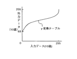
さて、昇華型カラープリンタなどの階調記録を行うプリンタでは、昇華リボンに塗布された昇華染料をサーマルヘッドにより加熱し、昇華染料の昇華作用により、被印字用紙(受容紙)に階調画像を形成する。この形成された階調画像の入力データに対する出力画像濃度の特性は図5に示す如くとなる。この図5において、たとえば、入力画像データを1画素8bit(256階調)とした場合、入力データの0〜68階調程度ではサーマルヘッドの発熱量が微小であるため、昇華リボンの染料を十分に昇華させることができず、この結果、画像がほとんど記録されないことになる。また、入力データの200〜255階調程度では、サーマルヘッドをさらに加熱しても、それ以上に出力画像濃度が高くならず、飽和状態となってしまうことになる。
【0004】
さらに、中間調部分では、図5に示すように、入力データに対する出力画像濃度は非常に立った状態の特性となるため、中間調部分において滑らかな画像を得ることができないといった不具合もあった。
【0005】
そこで、上記不具合を解消するために、従来は図6に示す如く、入力データに対してあらかじめ用意したγ変換テーブルを参照し、出力データを補正する、いわゆるガンマ変換補正を行っている。なお、通常、このガンマ変換は、入力データに対して記録された出力画像の明度特性あるいは濃度特性がリニアな状態となるように、入力データをROMにルックアップテーブルとして用意し、これを非線形変換して出力データを作成し、該出力データに基づいて画像形成を行っている。
【0006】
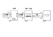
この従来におけるガンマ変換を用いた装置の概略構成を図7のブロック図に示す。図7において、701はγ変換テーブルデータを書き込んだROM、702はROM701を用いてガンマ変換し、出力されたデータを2値の256レベルのデータとして出力するサーマルヘッド駆動回路、703はサーマルヘッド駆動回路702からのデータに基づいて複数の発熱抵抗素子が駆動されるサーマルヘッドである。
【0007】
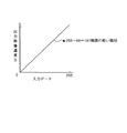
図7の構成において、γ変換テーブルデータを書き込んだROM701のアドレスに入力画像データを入力し、ガンマ変換を行う。ガンマ変換後の出力データを、サーマルヘッド駆動回路702によって、サーマルヘッドが印字可能な2値の256レベルのデータに変換し、1ライン周期間にサーマルヘッド703に256回レベルデータを転送し、印字する。このようにガンマ変換を行った場合における階調画像の入力データに対する出力画像濃度の特性は、概略的に見れば図8に示すように、リニアな特性となる。
【0008】
【発明が解決しようとする課題】
しかしながら、上記に示されるような従来の技術にあっては、256階調の入力データに対する出力データは、255−68=187階調程度しか使用することができないため、結果的に入力データの256階調をすべて表現することができず、図8に示す如く、粗い階段状の階調表現しか得ることができないという問題点があった。換言すれば、出力画像においては滑らかな階調変化部分に、疑似輪郭を生じさせるという画質低下を招来させていた。
【0009】
本発明は、上記に鑑みてなされたものであって、サーマルヘッドに印加する1階調印字あたりのエネルギー量を補正することにより、入力データが有する階調数を減らすことなく、かつ滑らかなガンマ変換を行い、出力画像の階調数を入力データの階調数のままの状態で表現し、画像品質の向上を図るサーマルヘッド駆動装置を提供することを第1の目的とする。
【0011】
【課題を解決するための手段】
上記の目的を達成するために、請求項1に係るサーマルヘッド駆動装置にあっては、サーマルヘッドを構成する複数の発熱抵抗素子を、多値の印字データに基づいて駆動するサーマルヘッド駆動装置において、入力される印字データに対し、前記サーマルヘッドにより印字・形成される画像の濃度特性がリニア特性となる1階調印字のストローブパルス幅データを格納した補正データ格納手段と、前記補正データ格納手段の前記ストローブパルス幅データを電圧変化を示すアナログのデータに変換するデータ変換手段と、前記データ変換手段が出力する前記電圧変化が予め定めた電圧レベルに達したか否かを監視する電圧レベル監視手段と、前記電圧レベル監視手段の電圧レベルが所定値以上の場合に制御信号を出力し、アナログのデータに変換された前記1階調印字のストローブパルス幅データを用い、印字する階調レベルに応じてヘッド駆動電圧を変化させるヘッド駆動手段と、を備えたものである。
【0012】
すなわち、請求項1のサーマルヘッド駆動装置によれば、補正データ格納手段に、入力される印字データに対し、サーマルヘッドが印字・形成する記録画像の明度特性あるいは濃度特性がリニアとなるような階調レベルに対応した印字エネルギー補正データを格納しておき、さらに、この印字エネルギー補正データを電圧変化データに変換し、該電圧変化データに基づいてサーマルヘッドが印字する階調レベルに応じて印字エネルギーを変化させ、サーマルヘッドを駆動することにより、入力画像データが有する階調数を減らすことのないガンマ変換が実現する。
【0021】
【発明の実施の形態】
以下、本発明に係るサーマルヘッド駆動装置について添付図面を参照し、詳細に説明する。
【0022】
(実施の形態1)
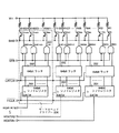
図1は、本発明のサーマルヘッド駆動装置が適用されるに好適なサーマルプリンタの電気的な概略構成を示すブロック図である。図において、101は制御プログラムに基づいて装置内の各部の制御を司るCPU、102はCPU101により1ライン分の多値データが書き込まれるバッファRAM(入力データ格納手段に該当する)、103はバッファRAM102に書き込んだ多値データを64バイトおきに16バイト読み出し、読み出した8bit/1画素の階調データを2値の256レベルデータに変換し、出力RAM104に書き込み、かつROM105に対してレベルカウント値を出力する2値化部(2値化手段に該当する)、104は階調データを2値の256レベルデータに変換する2値化部103でレベル変換された印字データを格納する出力RAM(出力データ格納手段に該当する)である。
【0023】
また、105はCPU101がバッファRAM102に書き込んだ印字データに対し、サーマルヘッド108により印字・形成される記録画像の明度特性あるいは濃度特性がリニアとなるような階調レベルに対応した ̄STBパルス幅テーブルが格納されているROM(補正データ格納手段に該当する)、106はストローブパスル ̄STB( ̄はLOWアクティブを示す)を発生してサーマルヘッド108に供給するストローブジェネレータ(エネルギー可変手段に該当する)である。
【0024】
また、107は内部システムクロック、ヘッドドライブ回路内の各種タイミング信号、およびサーマルヘッド108を駆動するタイミング信号(HCLK、ラッチパルス ̄LATCH( ̄はLOWアクティブを示す))を生成するタイミングコントローラ、108は昇華リボン(図示せず)を介して被印字用紙に熱定着を行うサーマルヘッド、109は印字モードにおいてサーマルヘッド108に対して駆動電圧を供給するヘッド駆動電源である。また、バス100にはCPU101およびバッファRAM102が接続されている。
【0025】
図2は、図1におけるサーマルヘッド108の詳細な回路構成例を示すものである。サーマルヘッドドライバー200が図2に示すように、1チップ64画素構成となっている。サーマルヘッド108へのデータ転送はHDATA1〜16のシリアルデータを16本パラレルで転送するように構成されている。
【0026】
詳述すれば、サーマルヘッド108は、ライン状に配置され、一端がVH ライン(電源ライン)に並列に接続され、他端がスイッチング回路TR1 〜TR1024に接続された複数の発熱抵抗素子R1〜R1024と、ヘッドドライブ回路(図示せず)から入力されるシリアルの印字データをパラレルのデータに変換する64bitシフトレジスタ201と、タイミングコントローラ107から供給されるラッチパルス ̄LATCH( ̄はLOWアクティブを示す)に基づいてラッチする64bitラッチ回路202とを備えている。
【0027】
さらに、64bitラッチ回路202の出力線とストローブジェネレータ106から供給される発熱抵抗素子R1〜R1024を駆動するためのストローブパルス ̄STBの供給線とに接続され、64bitラッチ回路202のラッチ信号 ̄LATCHとストローブパルス ̄STBとの論理積信号を出力するアンドゲートAND1 〜AND1024と、アンドゲートAND1 〜AND1024からの出力により開閉制御され、発熱抵抗素子R1〜R1024に記録電流を流すスイッチング回路TR1 〜TR1024と、を備えている。
【0028】
なお、スイッチング回路TR、アンドゲートAND、64bitシフトレジスタ201、64bitラッチ回路202は、図示の如く64bitごとにドライブICとして構成される。
【0029】
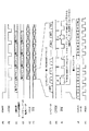
つぎに、以上のように構成されたサーマルプリンタの動作について、図1、図2と共に、図3に示すタイミングチャートを参照しながら説明する。図3において、(A)はCPU101から出力されるスタート信号 ̄STRT( ̄はLOWアクティブを示す)の波形、(B)はタイミングコントローラ107がCPU101に対して出力するライン同期割込信号 ̄LSYNCの波形、(C)は2値化部103のレベル変換動作を示す波形、(D)はサーマルヘッド108に対する転送データ、(E)はタイミングコントローラ107と2値化部103間によるHCLK、(F)はストローブジェネレータ106がサーマルヘッド108に対して出力するストローブパルス ̄STBである。
【0030】
また、(G)は2値化部103がROM105に出力するレベルデータ(レベルカウント値:ROM105のアドレス)、(H)はタイミングコントローラ107から出力されるラッチパルス ̄LATCHの波形、(I)は上記(F)の詳細な波形であり、ROM105のデータによりストローブジェネレータ106によって生成された可変デューティの印字ストローブパルス、(J)は1レベルデータを示すHDATA1〜16、(K)は上記(E)の1ラインあたりのHCLKの波形である。
【0031】
印字動作を行う場合、まず、CPU101はバッファRAM102に1ライン(この実施の形態では8bit/1画素の1024画素のデータ)分の多値の印字データを書き込み、タイミングコントローラ107に対し、図3(A)に示す如くスタート信号 ̄STRTをアクティブにし、印字動作のスタート指示を出力する。
【0032】
タイミングコントローラ107は、2値化部103を制御してバッファRAM102からCPU101が書き込んだデータを64バイトおきに16バイト読み出す。読み出された8bit/1画素の階調データは、2値化部103で16個のマグニチュードコンパレータで内部カウンタで発生した重みと比較し、2値の256レベルデータに変換して出力RAM104へ16bitで書き込む。以上の動作を64回行い、印字データを出力RAM104に準備する。
【0033】
つぎに、2値化部103は、出力RAM104から前ラインの第1レベルの16bitデータを64回順次読み出し、図3(J)に示す如くHDATA1〜HDATA16としてサーマルヘッド108へ転送する。
【0034】
サーマルヘッド108では、まず、64bitシフトレジスタ201が、供給されるクロック ̄HCLKのタイミングで、供給される1ライン分のデータを取り込み、64bitラッチ回路202に順次出力する。
【0035】
アンドゲートANDでは、64bitラッチ回路202から供給されるデータとストローブパルス ̄STBとの論理積が演算され、そこで得られる論理積信号が、スイッチング回路TRのトランジスタベースに出力される。これにより、トランジスタが動作し、トランジスタのコレクタに接続された発熱抵抗体Rが発熱し、1ラインごとの印字が行われる。
【0036】
この結果、昇華リボン(図示せず)の表面に塗布された昇華性インクが昇華し、記録紙に転写される。あるいは、感熱紙を用いた記録の場合には、サーマルヘッド108の発熱部分に該当する部分が発色し、記録紙に転写される。
【0037】
ところで、ここで本発明では、ストローブジェネレータ106により生成される1階調レベルのストローブパルス ̄STBのパルス幅(図3(I)参照)は、2値化部103が出力するレベルカウントの値をアドレスとしたROM105の出力データに基づいて決定される。
【0038】
ROM105には、CPU101がバッファRAM102に書き込んだ印字データに対し、サーマルヘッド108が印字して形成される記録画像の明度特性あるいは濃度特性がリニアとなるような階調レベルに対応した ̄STBパルス幅テーブルが格納されており、サーマルヘッド108が印字する階調レベルに応じてストローブパルス ̄STBのパルス幅を変化させる。つまり、サーマルヘッド108に加えるエネルギーを、印字される階調レベルに応じて変化させることによってガンマ変換を行う。
【0039】
また、この実施の形態では階調レベルに対応した ̄STBパルス幅テーブルをあらかじめ格納したROM105を用いているが、このROM105はRAMなどの記憶手段を用いて格納テーブルデータをCPU101がプリンタの初期化などに、プログラムが格納されたROM(図示せず)などから転送するように構成してもよい。
【0040】
以上説明したような、サーマルヘッド108に対するデータ転送動作および印字動作を第1階調レベルから第256階調レベルまで実行し、1ライン目の印字を終了すると共に、タイミングコントローラ107は、CPU101に対してライン同期割込信号 ̄LSYNC(図3(B)参照)をアサートし、次ラインの印字データの転送を要求する。
【0041】
この動作は、CPU101がスタート信号 ̄STRTをデアクティブにするまで継続され、被印字用紙および昇華リボン(いずれも図示せず)をライン同期割込信号 ̄LSYNCに同期させて搬送することにより、被印字用紙に階調画像が形成される。
【0042】
(実施の形態2)
この実施の形態2では、前述した実施の形態1に対し、1階調印字中のサーマルヘッドの駆動電圧を変化させることにより、ガンマ特性の変換を行う例について述べる。
【0043】
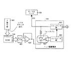
図4は、実施の形態2に係るサーマルプリンタの主要構成を示すブロック図である。図において、401はROM105が出力するデジタルデータをアナログデータ(電圧値を示すデータ)に変換するD/A変換器(データ変換手段に該当する)、402はD/A変換器401が出力する電圧を入力・保持するバッファである。
【0044】
また、ヘッド駆動電源109(ヘッド駆動手段に該当する)は、バッファ402を介してD/A変換器401が出力する電圧を入力し、その電圧が予め定めた設定電圧レベルに達したか否かを監視し、入力電圧レベルが設定電圧レベル以上の場合に光点灯することでトランジスタがONし、そのトランジスタによる信号をコントロール部404に供給するフォトカプラ403と、フォトカプラ403の出力に基づいてスイッチング部405を制御するコントロール部404と、コントロール部404の出力信号に基づいて供給する電源入力をスイッチングするスイッチング部405と、を備えている。なお、他の構成要素は前述した図1の構成と同一であるため、ここでは省略している。
【0045】
つぎに、以上のように構成されたサーマルプリンタの動作について説明する。図4において、まず、ROM105に格納してある1階調印字のストローブパルス幅テーブルからデータを出力する。この出力データはデジタルデータであるので、これをD/A変換器401によりアナログ変換(電圧変化を示すデータ)する。さらに、この電圧変化のデータを電圧安定化のためにバッファ402を介してヘッド駆動電源109のフォトカプラ403に供給する。
【0046】
すなわち、上記電圧変化をバッファ402を介してヘッド駆動電源109にフィードバックする。そして、その電圧が予め定めた設定電圧レベルに達したか否かを監視し、入力電圧レベルが設定電圧レベル以上の場合に光点灯することでトランジスタがONし、そのトランジスタによる信号をコントロール部404に供給する。コントロール部404は、フォトカプラ403の出力レベルに応じて制御信号を出力し、印字する階調レベルに応じたヘッド駆動電圧VH を変化させることにより、サーマルヘッド108に加える印字エネルギーを階調ごとに変化させて、ガンマ変換を行う。
【0047】
つぎに、この実施の形態1、2が奏する効果について述べる。まず、従来のガンマ変換は、入力画像データをγ変換テーブルに基づいて変換し、これを出力画像データとしていたため、出力画像の階調性が減少し、その結果、滑らかな階調表現を行うことが困難である旨については先に述べた通りである。
【0048】
これに対し、この実施の形態では、ROM105に、入力画像データに対し、サーマルヘッド108が印字・形成する記録画像の明度特性あるいは濃度特性がリニアとなるような階調レベルに対応した印字エネルギー補正データ(ストローブパルス幅データ、ヘッド電源電圧データ)を格納しておき、この格納された印字エネルギー補正データを用い、サーマルヘッド108に印加する印字エネルギーを印字される階調レベルに応じて変化させることにより、入力画像データが有する階調数を減らすことのないガンマ変換が実現する。
【0049】
したがって、入力画像データのもつ階調数をそのままの状態で画像出力することになり、滑らかな階調変化をそのまま表現することが可能となり、非常に高品位の記録画像を提供することができる。
【0050】
【発明の効果】
以上説明したように、本発明に係るサーマルヘッド駆動装置(請求項1)によれば、正データ格納手段に、入力される印字データに対し、サーマルヘッドが印字・形成する記録画像の明度特性あるいは濃度特性がリニアとなるような階調レベルに対応した印字エネルギー補正データを格納しておき、さらに、この印字エネルギー補正データを電圧変化データに変換し、該電圧変化データに基づいてサーマルヘッドが印字する階調レベルに応じて印字エネルギーを変化させ、サーマルヘッドを駆動するため、入力画像データが有する階調数を減らすことのないガンマ変換が実現し、入力画像データのもつ階調数をそのままの状態で画像出力することになり、滑らかな階調変化をそのまま表現することが可能となり、非常に高品位の記録画像が得られるサーマルヘッド駆動装置を提供することができる。
【図面の簡単な説明】
【図1】本発明のサーマルヘッド駆動装置が適用されるに好適なサーマルプリンタの電気的な概略構成を示すブロック図である。
【図2】図1におけるサーマルヘッドの詳細な回路構成例を示すものである。
【図3】本発明による実施の形態に係るサーマルヘッドの駆動タイミングを示すフローチャートである。
【図4】本発明による実施の形態2に係るサーマルプリンタの主要構成を示すブロック図である。
【図5】従来における階調画像の入力データに対する出力画像濃度の特性(ガンマ補正前)を示すグラフである。
【図6】従来におけるガンマ変換補正例を示すグラフである。
【図7】従来におけるガンマ変換によるサーマルヘッド駆動装置の構成を示すブロック図である。
【図8】従来におけるガンマ変換補正を行った場合の階調画像の入力データに対する出力画像濃度の特性を示すグラフである。
【符号の説明】
101 CPU
102 バッファRAM
103 2値化部
104 出力RAM
105 ROM
106 ストローブジェネレータ
107 タイミングコントローラ
108 サーマルヘッド
109 ヘッド駆動電源
200 サーマルヘッドドライバ
201 64bitシフトレジスタ
202 64bitラッチ回路
401 D/A変換器
402 バッファ
403 フォトカプラ
404 コントロール部
405 スイッチング部[0001]
[Technical field to which the invention belongs]
The present invention relates to a thermal head driving device and a thermal printer that are used in various printers that form a gradation image using a thermal head, and more specifically, to a thermal head instead of gamma conversion correction by print data. the amount of energy per one gradation printing is corrected, without decreasing the number of gradations included in the input data, and relates to a thermal head drive equipment to perform a smooth gamma conversion.
[0002]
[Prior art]
For example, in a thermal head, heating resistors are formed in a line at regular intervals, and recording is performed using Joule heat generated by the heating resistors. Recording with a thermal head is roughly divided into a thermal recording system and a thermal transfer system, and has the features of simple structure, excellent maintainability, operability and quietness, and economical and high reliability. Furthermore, since the recording from monochrome images to color images is possible, the applications have been expanded. For this reason, facsimiles, ticket vending machines, output devices for personal computers and video devices, electronic blackboards, recording devices for OA related equipment, Are widely used in various devices.
[0003]
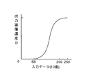
In a printer that performs gradation recording such as a sublimation type color printer, the sublimation dye applied to the sublimation ribbon is heated by a thermal head, and the sublimation action of the sublimation dye causes a gradation image to be printed on the printing paper (receiving paper). Form. The characteristic of the output image density with respect to the input data of the formed gradation image is as shown in FIG. In FIG. 5, for example, when the input image data is 8 bits (256 gradations) per pixel, the thermal head generates a small amount of heat when the input data is about 0 to 68 gradations. As a result, almost no image is recorded. In addition, when the input data is about 200 to 255 gradations, even if the thermal head is further heated, the output image density is not further increased, and the saturated state is reached.
[0004]
Further, in the halftone portion, as shown in FIG. 5, since the output image density with respect to the input data has a very standing characteristic, there is a problem that a smooth image cannot be obtained in the halftone portion.
[0005]
Therefore, in order to solve the above problems, conventionally, as shown in FIG. 6, a so-called gamma conversion correction is performed in which output data is corrected by referring to a γ conversion table prepared for input data in advance. Normally, this gamma conversion is performed by preparing input data as a look-up table in ROM so that the brightness characteristic or density characteristic of the output image recorded with respect to the input data is in a linear state, which is converted into a non-linear conversion. Thus, output data is created, and image formation is performed based on the output data.
[0006]
A schematic configuration of this conventional apparatus using gamma conversion is shown in a block diagram of FIG. In FIG. 7,
[0007]
In the configuration of FIG. 7, input image data is input to the address of the
[0008]
[Problems to be solved by the invention]
However, in the conventional technique as described above, output data corresponding to 256-gradation input data can only use about 255-68 = 187 gradations. There is a problem that not all gradations can be expressed, and only a rough stepped gradation expression can be obtained as shown in FIG. In other words, in the output image, the image quality is reduced such that a pseudo contour is generated in a smooth gradation changing portion.
[0009]
The present invention has been made in view of the above, and by correcting the amount of energy per gradation printing applied to the thermal head, smooth gamma can be achieved without reducing the number of gradations of the input data. It is a first object of the present invention to provide a thermal head driving device that performs conversion and expresses the number of gradations of an output image as it is in the number of gradations of input data to improve the image quality.
[0011]
[Means for Solving the Problems]
In order to achieve the above object, in the thermal head driving device according to
[0012]
In other words, according to the thermal head drive device of the first aspect, the correction data storage means is such that the brightness characteristic or density characteristic of the recorded image printed and formed by the thermal head is linear with respect to the print data input. The printing energy correction data corresponding to the tone level is stored , the printing energy correction data is converted into voltage change data, and the printing energy is changed according to the gradation level printed by the thermal head based on the voltage change data. By changing the above and driving the thermal head, gamma conversion without reducing the number of gradations of the input image data is realized.
[0021]
DETAILED DESCRIPTION OF THE INVENTION
Hereinafter, with reference to the accompanying drawings with the thermal head driving equipment according to the present invention will be described in detail.
[0022]
(Embodiment 1)
FIG. 1 is a block diagram showing an electrical schematic configuration of a thermal printer suitable for application of the thermal head driving apparatus of the present invention. In the figure, 101 is a CPU that controls each part in the apparatus based on a control program, 102 is a buffer RAM (corresponding to input data storage means) in which multi-value data for one line is written by the
[0023]
[0024]
A timing controller 107 generates an internal system clock, various timing signals in the head drive circuit, and a timing signal for driving the thermal head 108 (HCLK, latch pulse を LATCH ( ̄ indicates LOW active)), 108 A
[0025]
FIG. 2 shows a detailed circuit configuration example of the
[0026]
More specifically, the
[0027]
Further, the output line of the 64-
[0028]
Note that the switching circuit TR, the AND gate AND, the 64-
[0029]
Next, the operation of the thermal printer configured as described above will be described with reference to the timing chart shown in FIG. 3 together with FIGS. 3, (A) shows the waveform of the start signal  ̄STRT ( ̄ indicates LOW active) output from the
[0030]
(G) is level data (level count value: address of ROM 105) output from the
[0031]
When performing the printing operation, first, the
[0032]
The timing controller 107 controls the
[0033]
Next, the
[0034]
In the
[0035]
In the AND gate AND, the logical product of the data supplied from the 64-
[0036]
As a result, the sublimable ink applied to the surface of the sublimation ribbon (not shown) sublimates and is transferred to the recording paper. Alternatively, in the case of recording using thermal paper, the portion corresponding to the heat generating portion of the
[0037]
By the way, in the present invention, the pulse width (see FIG. 3I) of the strobe pulse  ̄STB of one gradation level generated by the
[0038]
The
[0039]
In this embodiment, the
[0040]
As described above, the data transfer operation and the printing operation for the
[0041]
This operation is continued until the
[0042]
(Embodiment 2)
In the second embodiment, an example in which the gamma characteristic is converted by changing the driving voltage of the thermal head during one gradation printing will be described with respect to the first embodiment.
[0043]
FIG. 4 is a block diagram showing the main configuration of the thermal printer according to the second embodiment. In the figure, 401 is a D / A converter (corresponding to data conversion means) that converts digital data output from the
[0044]
The head drive power supply 109 (corresponding to the head drive means) receives a voltage output from the D /
[0045]
Next, the operation of the thermal printer configured as described above will be described. In FIG. 4, first, data is output from the strobe pulse width table for one gradation printing stored in the
[0046]
That is, feeding back the voltage change to the head
[0047]
Next, effects obtained by the first and second embodiments will be described. First, in the conventional gamma conversion, input image data is converted based on a γ conversion table and used as output image data. As a result, the gradation of the output image is reduced, resulting in smooth gradation expression. This is difficult as described above.
[0048]
On the other hand, in this embodiment, the printing energy correction corresponding to the gradation level in which the brightness characteristic or density characteristic of the recorded image printed and formed by the
[0049]
Therefore, the image is output with the number of gradations of the input image data as it is, so that a smooth gradation change can be expressed as it is, and a very high-quality recorded image can be provided.
[0050]
【The invention's effect】
As described above, according to the thermal head driving device (claim 1) of the present invention, the brightness characteristics of the recorded image printed or formed by the thermal head on the print data input to the positive data storage means or be stored the printing energy correction data density characteristic corresponding to the grayscale level such that a linear, is La, converts the printing energy correction data voltage variation data, a thermal head on the basis of the voltage change data Since the print energy is changed according to the gradation level printed by the printer and the thermal head is driven, gamma conversion without reducing the number of gradations of the input image data is realized, and the number of gradations of the input image data is reduced. The image is output as it is, and it is possible to express smooth gradation changes as they are, and a very high-quality recorded image can be obtained. It is possible to provide a thermal head driving device.
[Brief description of the drawings]
FIG. 1 is a block diagram showing an electrical schematic configuration of a thermal printer suitable for application of a thermal head driving device of the present invention.
FIG. 2 shows a detailed circuit configuration example of the thermal head in FIG. 1;
FIG. 3 is a flowchart showing drive timing of a thermal head according to an embodiment of the present invention.
FIG. 4 is a block diagram showing a main configuration of a thermal printer according to a second embodiment of the present invention.
FIG. 5 is a graph showing characteristics of output image density (before gamma correction) with respect to input data of a conventional gradation image.
FIG. 6 is a graph showing a conventional gamma conversion correction example.
FIG. 7 is a block diagram illustrating a configuration of a conventional thermal head driving apparatus using gamma conversion.
FIG. 8 is a graph showing characteristics of output image density with respect to input data of a gradation image when conventional gamma conversion correction is performed.
[Explanation of symbols]
101 CPU
102 Buffer RAM
103
105 ROM
106 Strobe Generator 107
Claims (1)
入力される印字データに対し、前記サーマルヘッドにより印字・形成される画像の濃度特性がリニア特性となる1階調印字のストローブパルス幅データを格納した補正データ格納手段と、
前記補正データ格納手段の前記ストローブパルス幅データを電圧変化を示すアナログのデータに変換するデータ変換手段と、
前記データ変換手段が出力する前記電圧変化が予め定めた電圧レベルに達したか否かを監視する電圧レベル監視手段と、
前記電圧レベル監視手段の電圧レベルが所定値以上の場合に制御信号を出力し、アナログのデータに変換された前記1階調印字のストローブパルス幅データを用い、印字する階調レベルに応じてヘッド駆動電圧を変化させるヘッド駆動手段と、
を備えたことを特徴とするサーマルヘッド駆動装置。In a thermal head drive device that drives a plurality of heating resistance elements constituting a thermal head based on multi-value print data,
Correction data storage means for storing strobe pulse width data for one-gradation printing in which density characteristics of an image printed and formed by the thermal head are linear characteristics with respect to input print data;
Data conversion means for converting the strobe pulse width data of the correction data storage means into analog data indicating a voltage change;
Voltage level monitoring means for monitoring whether the voltage change output by the data conversion means has reached a predetermined voltage level;
A control signal is output when the voltage level of the voltage level monitoring means is greater than or equal to a predetermined value, and the head is used in accordance with the gradation level to be printed using the strobe pulse width data of the one gradation printing converted to analog data Head drive means for changing the drive voltage;
A thermal head driving device comprising:
Priority Applications (1)
| Application Number | Priority Date | Filing Date | Title |
|---|---|---|---|
| JP28212497A JP4046816B2 (en) | 1997-10-15 | 1997-10-15 | Thermal head drive device |
Applications Claiming Priority (1)
| Application Number | Priority Date | Filing Date | Title |
|---|---|---|---|
| JP28212497A JP4046816B2 (en) | 1997-10-15 | 1997-10-15 | Thermal head drive device |
Publications (2)
| Publication Number | Publication Date |
|---|---|
| JPH11115234A JPH11115234A (en) | 1999-04-27 |
| JP4046816B2 true JP4046816B2 (en) | 2008-02-13 |
Family
ID=17648441
Family Applications (1)
| Application Number | Title | Priority Date | Filing Date |
|---|---|---|---|
| JP28212497A Expired - Fee Related JP4046816B2 (en) | 1997-10-15 | 1997-10-15 | Thermal head drive device |
Country Status (1)
| Country | Link |
|---|---|
| JP (1) | JP4046816B2 (en) |
Families Citing this family (2)
| Publication number | Priority date | Publication date | Assignee | Title |
|---|---|---|---|---|
| JP4726313B2 (en) * | 2001-03-21 | 2011-07-20 | 日本信号株式会社 | Card processing system with display function |
| JP3803644B2 (en) | 2003-02-27 | 2006-08-02 | Necインフロンティア株式会社 | Gradation control method and gradation control method |
-
1997
- 1997-10-15 JP JP28212497A patent/JP4046816B2/en not_active Expired - Fee Related
Also Published As
| Publication number | Publication date |
|---|---|
| JPH11115234A (en) | 1999-04-27 |
Similar Documents
| Publication | Publication Date | Title |
|---|---|---|
| US4819008A (en) | Thermal head driver circuit | |
| JP2619890B2 (en) | Head drive for thermal transfer printer | |
| JP2896249B2 (en) | Printer recording head drive | |
| JP4046816B2 (en) | Thermal head drive device | |
| JPH1134383A (en) | Thermal head driving device and thermal head driving method | |
| JPH06340105A (en) | Driving of thermal head | |
| JPS61220563A (en) | Multigradation recording device | |
| JP2001130042A (en) | Method and apparatus for controlling driving thermal head | |
| JPH0236958A (en) | Power conduction control method in multi-gradation thermal recording | |
| JP4385459B2 (en) | Thermal head control device and control method thereof | |
| JP2008279684A (en) | Printer, printer control method, printer control program | |
| JP2001180030A (en) | Thermal head and thermal printer | |
| JP5830759B2 (en) | Apparatus for supplying a signal for generating a multi-tone image | |
| JPH058427A (en) | Printer device | |
| KR0132893B1 (en) | Video printer device | |
| JP5574347B2 (en) | Device having a unit for controlling a thermal head | |
| JPH04104452U (en) | thermal line printer | |
| JPH03224754A (en) | Density gradation control-type thermal printer and current value detection device | |
| JP2006321191A (en) | Thermal printer | |
| JPH04345861A (en) | Thermal transfer recorder | |
| JPS62224166A (en) | Thermosensitive recorder | |
| JP2008279683A (en) | Printer, printer control method, printer control program | |
| JPS63256464A (en) | Thermal recorder | |
| JPH01196366A (en) | Printing head control device | |
| JPH07156434A (en) | Printing equipment |
Legal Events
| Date | Code | Title | Description |
|---|---|---|---|
| A621 | Written request for application examination |
Effective date: 20040930 Free format text: JAPANESE INTERMEDIATE CODE: A621 |
|
| A977 | Report on retrieval |
Effective date: 20060922 Free format text: JAPANESE INTERMEDIATE CODE: A971007 |
|
| A131 | Notification of reasons for refusal |
Free format text: JAPANESE INTERMEDIATE CODE: A131 Effective date: 20060926 |
|
| A521 | Written amendment |
Free format text: JAPANESE INTERMEDIATE CODE: A523 Effective date: 20061124 |
|
| A131 | Notification of reasons for refusal |
Effective date: 20070508 Free format text: JAPANESE INTERMEDIATE CODE: A131 |
|
| A521 | Written amendment |
Effective date: 20070618 Free format text: JAPANESE INTERMEDIATE CODE: A523 |
|
| TRDD | Decision of grant or rejection written | ||
| A01 | Written decision to grant a patent or to grant a registration (utility model) |
Free format text: JAPANESE INTERMEDIATE CODE: A01 Effective date: 20071120 |
|
| A61 | First payment of annual fees (during grant procedure) |
Free format text: JAPANESE INTERMEDIATE CODE: A61 Effective date: 20071121 |
|
| FPAY | Renewal fee payment (prs date is renewal date of database) |
Year of fee payment: 3 Free format text: PAYMENT UNTIL: 20101130 |
|
| R150 | Certificate of patent (=grant) or registration of utility model |
Free format text: JAPANESE INTERMEDIATE CODE: R150 |
|
| FPAY | Renewal fee payment (prs date is renewal date of database) |
Free format text: PAYMENT UNTIL: 20101130 Year of fee payment: 3 |
|
| FPAY | Renewal fee payment (prs date is renewal date of database) |
Free format text: PAYMENT UNTIL: 20111130 Year of fee payment: 4 |
|
| LAPS | Cancellation because of no payment of annual fees |