JP3849842B2 - Flux for soldering, solder paste, electronic component device, electronic circuit module, electronic circuit device, and soldering method - Google Patents
Flux for soldering, solder paste, electronic component device, electronic circuit module, electronic circuit device, and soldering method Download PDFInfo
- Publication number
- JP3849842B2 JP3849842B2 JP2000218046A JP2000218046A JP3849842B2 JP 3849842 B2 JP3849842 B2 JP 3849842B2 JP 2000218046 A JP2000218046 A JP 2000218046A JP 2000218046 A JP2000218046 A JP 2000218046A JP 3849842 B2 JP3849842 B2 JP 3849842B2
- Authority
- JP
- Japan
- Prior art keywords
- flux
- soldering
- electronic circuit
- solder
- solder paste
- Prior art date
- Legal status (The legal status is an assumption and is not a legal conclusion. Google has not performed a legal analysis and makes no representation as to the accuracy of the status listed.)
- Expired - Lifetime
Links
Images


Classifications
-
- H—ELECTRICITY
- H01—ELECTRIC ELEMENTS
- H01L—SEMICONDUCTOR DEVICES NOT COVERED BY CLASS H10
- H01L2224/00—Indexing scheme for arrangements for connecting or disconnecting semiconductor or solid-state bodies and methods related thereto as covered by H01L24/00
- H01L2224/01—Means for bonding being attached to, or being formed on, the surface to be connected, e.g. chip-to-package, die-attach, "first-level" interconnects; Manufacturing methods related thereto
- H01L2224/10—Bump connectors; Manufacturing methods related thereto
- H01L2224/15—Structure, shape, material or disposition of the bump connectors after the connecting process
- H01L2224/16—Structure, shape, material or disposition of the bump connectors after the connecting process of an individual bump connector
- H01L2224/161—Disposition
- H01L2224/16151—Disposition the bump connector connecting between a semiconductor or solid-state body and an item not being a semiconductor or solid-state body, e.g. chip-to-substrate, chip-to-passive
- H01L2224/16221—Disposition the bump connector connecting between a semiconductor or solid-state body and an item not being a semiconductor or solid-state body, e.g. chip-to-substrate, chip-to-passive the body and the item being stacked
- H01L2224/16225—Disposition the bump connector connecting between a semiconductor or solid-state body and an item not being a semiconductor or solid-state body, e.g. chip-to-substrate, chip-to-passive the body and the item being stacked the item being non-metallic, e.g. insulating substrate with or without metallisation
-
- H—ELECTRICITY
- H01—ELECTRIC ELEMENTS
- H01L—SEMICONDUCTOR DEVICES NOT COVERED BY CLASS H10
- H01L2224/00—Indexing scheme for arrangements for connecting or disconnecting semiconductor or solid-state bodies and methods related thereto as covered by H01L24/00
- H01L2224/01—Means for bonding being attached to, or being formed on, the surface to be connected, e.g. chip-to-package, die-attach, "first-level" interconnects; Manufacturing methods related thereto
- H01L2224/26—Layer connectors, e.g. plate connectors, solder or adhesive layers; Manufacturing methods related thereto
- H01L2224/31—Structure, shape, material or disposition of the layer connectors after the connecting process
- H01L2224/32—Structure, shape, material or disposition of the layer connectors after the connecting process of an individual layer connector
- H01L2224/321—Disposition
- H01L2224/32151—Disposition the layer connector connecting between a semiconductor or solid-state body and an item not being a semiconductor or solid-state body, e.g. chip-to-substrate, chip-to-passive
- H01L2224/32221—Disposition the layer connector connecting between a semiconductor or solid-state body and an item not being a semiconductor or solid-state body, e.g. chip-to-substrate, chip-to-passive the body and the item being stacked
- H01L2224/32225—Disposition the layer connector connecting between a semiconductor or solid-state body and an item not being a semiconductor or solid-state body, e.g. chip-to-substrate, chip-to-passive the body and the item being stacked the item being non-metallic, e.g. insulating substrate with or without metallisation
-
- H—ELECTRICITY
- H01—ELECTRIC ELEMENTS
- H01L—SEMICONDUCTOR DEVICES NOT COVERED BY CLASS H10
- H01L2224/00—Indexing scheme for arrangements for connecting or disconnecting semiconductor or solid-state bodies and methods related thereto as covered by H01L24/00
- H01L2224/73—Means for bonding being of different types provided for in two or more of groups H01L2224/10, H01L2224/18, H01L2224/26, H01L2224/34, H01L2224/42, H01L2224/50, H01L2224/63, H01L2224/71
- H01L2224/732—Location after the connecting process
- H01L2224/73201—Location after the connecting process on the same surface
- H01L2224/73203—Bump and layer connectors
- H01L2224/73204—Bump and layer connectors the bump connector being embedded into the layer connector
Description
【0001】
【発明の属する技術分野】
本発明は、はんだ付け用フラックス、はんだぺ一スト、電子部品装置、電子回路モジュール、電子回路装置、及び、はんだ付け方法に関する。
【0002】
【従来の技術】
例えば、部品搭載基板に対する部品のはんだ付けに当たっては、周知のように、フラックスが用いられる。フラックスの主な機能は、部品搭載基板に設けられた金属導体及び部品のはんだ付け用金属の表面の酸化皮膜を除去し、はんだの濡れ性を向上させることにある。フラックスとしては、ロジンを主成分とするものが最もよく知られている。ロジンには、アビエチン酸、レボビマル酸等のカルボン酸が含まれており、カルボキシル基の働きにより、はんだ付けされる金属表面の酸化膜を除去する。
【0003】
フラックスには、通常、上述したロジンの外、印刷性の向上及び仮止め強度を得る目的で、溶剤、可塑剤またはチキソ剤等の各種の添加物が配合される。例えば、特開平11−121915号公報は、粘性を、アルコール添加によって調整するタイプのフラックスを開示している。
【0004】
更に、別のフラックスとして、ミル規格で規定されているRMA(ハロゲンフリー)系フラックスも知られている。このフラックスの場合、リフロー後、フラックス等の洗浄工程が省略される。
【0005】
上述したフラックスは、はんだ付け後は、はんだ付けされた部品の接着に関与せず、はんだ接合は、はんだ金属の溶融接合によって達成される。従って、はんだ付けされる金属間の接合強度は、はんだ接合面積に依存する。
【0006】
ところが、各種電子機器において、高密度実装が進むにつれ、部品が小型化され、部品の配置間隔が狭ピッチ化され、これに伴い、はんだ接合面積の狭小化が急速に進展しつつあり、現段階でも、既に、十分なはんだ付け強度を確保することが困難になっている。しかも、実装の高密度化、部品の小型化及び部品の配置間隔の狭ピッチ化は、更に進展する傾向にあり、はんだ接合面積のみによってはんだ接合強度を確保する従来手段では、この技術動向に対応することが、ますます困難になる傾向にある。
【0007】
一般に、はんだ接合強度を確保する手段として、はんだのフィレット部を形成し、部品の端子と部品搭載基板上の導体(ランドまたははんだバンプ)とのはんだ接合面積を拡大する手段が採られている。ところが、高密度実装においては、フィレット部の接合面積も小さくなってしまうため、フィレット部による接合強度の増大手段も採りにくい。
【0008】
また、例えば、各種の電子回路モジュールでは、両面実装タイプの部品搭載基板を用い、部品搭載基板の一面上に高温はんだを用いて部品をはんだ付け(通炉)した後、他面に部品を搭載し、再び通炉する。従って、部品搭載基板の他面側における部品のはんだ付けに当たっては、一面側の高温はんだよりも低い融点を持つ低温はんだを用いてはんだ付けする必要がある。従来、はんだの融点はPbの含有量によって調整するのが一般的であった。
【0009】
ところが、地球環境保全の立場から、Pbを含有しないはんだ(Pbフリーはんだ)が要求され、そのようなはんだ組成の開発が盛んに行われている。しかし、Pbフリーはんだで、従来の高温はんだに匹敵する高温融点のはんだ組成は、現在のところ、実用化されていない。理由として、Pbフリーはんだ自体の融点が220℃前後と、共晶はんだに比較し、約40℃も上昇するため、Pb以外の代替組成が見つからないからである。このため、両面実装タイプの部品搭載基板において、両面側で用いられるはんだの融点差を十分にとることができず、部品を部品搭載基板上に実装する際、部品が浮動し、または脱落する等の不具合が生じる。
【0010】
更に、半導体チップを用いた電子回路モジュールにおいては、半導体チップをチップ搭載基板にはんだ付けした後、封止剤を接合界面に流し込み、半導体チップと、チップ搭載基板とを封止剤で接着固定する作業が付加される。
【0011】
ところが、封止剤注入時にフラックスの残渣が残っていると、フラックスのために、封止剤が半導体チップと基板との間の界面に十分に到達せず、接着力が発揮できない。そこで、封止剤を注入する前、フラックスを洗浄する工程が付加される。フラックスの洗浄は、通常、揮発性有機溶剤を用い、数回に分けて行なわれる。ところが、環境保全等の目的から、揮発性有機溶剤の使用が規制されており、フラックスの洗浄工程は、コストおよび環境保全の両面から、負担の大きい工程となっている。
【0012】
更に、上述のようにして得られた電子回路モジュールをマザー基板に搭載して、電子回路装置を構成する場合、チップ搭載基板にセラミックを用い、マザー基板に有機樹脂基板を用いた組み合わせにおいては、搭載後の熱衝撃試験などにおいて、セラミック基板及び有機樹脂基板の熱膨張率の違いから、はんだ接合部に収縮応力が集中し、クラックが入り易く、接合寿命が短いとされている。よってはんだ接合強度向上を図るため、封止剤の注入を行ないたいが、マザー基板全体を、フラックス洗浄工程及び封止剤注入工程に付することは、かなりのコストアップを招くため、実際には行われていない。
【0013】
【発明が解決しようとする課題】
本発明の課題は、実装の高密度化、部品の小型化及び部品の配置間隔の狭ピッチ化等に対しても、十分な接合強度をもって対応し得るはんだ付け用フラックス及びはんだペースト及びはんだ付け方法を提供することである。
【0014】
本発明のもう一つの課題は、両面実装タイプの部品搭載基板において、両面側で用いられるはんだの融点差を十分にとらなくとも、部品の浮動または脱落等の不具合を確実に阻止し得るはんだ付け用フラックス及びはんだペースト及びはんだ付け方法を提供することである。
【0015】
本発明の更にもう一つの課題は、フラックス洗浄工程を必要とせず、製造コストの安価な電子部品装置、電子回路モジュール及び電子回路装置を提供することである。
【0016】
本発明の更にもう一つの課題は、はんだ接合寿命を、従来よりも著しく長期化させた高信頼度の電子部品装置、電子回路モジュール及び電子回路装置を提供することである。
【0017】
【課題を解決するための手段】
上述した課題を解決するため、本発明に係るはんだ付け用フラックスは、接着性樹脂と硬化剤とを含有する。
【0018】
本発明に係るフラックスは、接着性樹脂と、硬化剤とを含有するから、はんだ付け後に、接着性樹脂を、部品搭載基板と部品を固定する接着剤として機能させることができる。このため、衝撃や熱ストレスに対し、部品の剥離、脱落を防ぎ、はんだ接合の信頼性を向上させることができる。この点、はんだ付け後に、接着機能を持たない従来のロジン系フラックスと著しく異なる。
【0019】
しかも、本発明に係るフラックスを使用することにより、フィレット部がなくても、十分な固着強度を確保できる。このため、部品搭載基板上に形成される部品接続用導体(ランド)に、フィレット部を生じさせるための領域を設ける必要がなくなるので、実装密度を向上させることが可能となる。
【0020】
本発明に係るフラックスにおいて、接着性樹脂としては、多数の樹脂材料から、温度に応じて、高い接着力を示す樹脂を選択し、これを接着性樹脂として用いることができる。従って、両面実装タイプの部品搭載基板の1面目に本発明に係るフラックスを用いて、部品をはんだ付けした後、部品搭載基板の2面目に通常の共晶はんだを用い、リフロー炉を通炉した場合でも、1面目に搭載された部品がシフティング、マンハッタン現象(部品立ち現象)または脱落等の不具合を起こすことはない。勿論、1面目及び2面目の両はんだ付け処理において、本発明に係るフラックスを用いることができる。
【0021】
本発明に係るフラックスは液状またはペーストの形態を採ることができる。このようなフラックスは、印刷、ディスペンサー塗布、スプレー、はけ塗り等の手段によって、部品搭載基板等に容易に塗布できる。
【0022】
本発明に係るフラックスにおいて、好ましい接着性樹脂は、熱硬化性樹脂である。熱硬化性樹脂の具体例としては、エポキシ樹脂、フェノール樹脂、ポリイミド樹脂、シリコン樹脂または変性樹脂またはアクリル樹脂から選択された少なくとも1種を挙げることができる。例示された樹脂材料の種類及び配合量は、接着温度帯及び目標とする皮膜硬度等に応じて選択することができる。
【0023】
硬化剤は、接着性樹脂を硬化させるものであればよい。好ましくは、カルボン酸を含む。カルボン酸を含む硬化剤は、熱硬化性樹脂に対する硬化作用のみならず、はんだ付けされる金属表面の酸化膜を除去するフラックス作用も兼ね備える。
【0024】
本発明に係るフラックスは、溶剤、可塑剤及びチキソ剤等を含んでいてもよい。溶剤は、接着性樹脂の硬化温度及び硬化速度を調整すると共に、塗布形態に応じて粘度を調整するために加えられる。可塑剤及びチキソ剤も、塗布形態に応じて、粘度を調整するために加えられる。溶剤、可塑剤及びチキソ剤等は、その使用目的に合うように、配合量が選択される。
【0025】
本発明に係るフラックスは、接着性樹脂、還元作用をもたらす有機酸、カルボン酸、溶剤または硬化剤を封入したマイクロカプセルの形態であってもよい。
【0026】
更に、本発明に係るフラックスは、はんだ粉末と混合して、はんだペーストを構成するために用いることもできる。はんだ粉末は、Sn、Cu、Ag、Sb、Pb、In、Zn及びBiから選択することができる。Pbフリーのはんだペーストを得る場合には、はんだ粉末はPb以外のはんだ粉末で構成する。
【0027】
本発明は、更に、上述したフラックスを用いた電子部品装置、電子回路モジュール及び電子回路装置を開示する。まず、本発明に係る電子部品装置は、少なくとも1つの電子部品と、部品搭載基板と、はんだ付け用フラックスとを含む。前記電子部品は、部品搭載基板の上にはんだ付けされている。前記はんだ付け用フラックスは、接着性樹脂と、硬化剤とを含有し、前記電子部品と前記部品搭載基板との間に介在し、両者を接着している。
【0028】
前記電子部品と前記部品搭載基板との間に介在するはんだ付け用フラックスは、接着性樹脂と、硬化剤とを含有しており、接着剤として機能する。このはんだ付け用フラックスは洗浄する必要がなく、そのまま接着はんだ付け用フラックスとして用いることができる。従って、フラックス洗浄工程を必要とせず、製造コストの安価な電子部品装置を得ることができる。しかも、はんだ付け用フラックスは、接着性樹脂と、硬化剤とを含有しており、接着剤として機能するから、はんだ接合寿命を、従来よりも著しく長期化させた高信頼度の電子部品装置を得ることができる。
【0029】
次に、本発明に係る電子回路モジュールは、半導体チップと、チップ搭載基板と、はんだ付け用フラックスとを含む。前記半導体チップは、少なくとも1つの半導体素子を含み、チップ搭載基板の上にはんだ付けされている。前記はんだ付け用フラックスは、接着性樹脂と、硬化剤とを含有し、前記半導体チップと前記チップ搭載基板との間に介在し、両者を接着している。
【0030】
前記半導体チップと前記チップ搭載基板との間に介在するはんだ付け用フラックスは、接着性樹脂と、硬化剤とを含有しており、接着剤として機能する。このはんだ付け用フラックスは洗浄する必要がなく、そのまま接着はんだ付け用フラックスとして用いることができる。従って、フラックス洗浄工程を必要とせず、製造コストの安価な電子回路モジュールを得ることができる。しかも、はんだ付け用フラックスは、接着性樹脂と、硬化剤とを含有しており、接着剤として機能するから、はんだ接合寿命を、従来よりも著しく長期化させた高信頼度の電子回路モジュールを得ることができる。
【0031】
更に、本発明に係る電子回路装置は、電子回路モジュールと、マザー基板と、はんだ付け用フラックスとを含む。前記電子回路装置は、前記マザー基板上にはんだ付けされている。前記はんだ付け用フラックスは、接着性樹脂と、硬化剤とを含有し、前記半導体チップと前記マザー基板との間に介在し、両者を接着している。このはんだ付け用フラックスは洗浄する必要がなく、そのまま接着はんだ付け用フラックスとして用いることができる。従って、フラックス洗浄工程を必要としないから、製造コストの安価な電子回路装置を得ることができる。しかも、はんだ付け用フラックスは、接着性樹脂と、硬化剤とを含有しており、接着剤として機能するから、はんだ接合寿命を、従来よりも著しく長期化させた高信頼度の電子回路装置を得ることができる。
【0032】
本発明は、更に、上述したフラックス及びはんだペーストを用いたはんだ付け方法についても開示する。
【0033】
【発明の実施の形態】
<フラックス、電子部品装置>
実施例1
熱硬化性樹脂としてビスフェノールAを用い、硬化剤にはカルボン酸の無水物を使用した。熱硬化性樹脂及び硬化剤の配合比は重量比で1:1とした。また、粘性を確保するために、少量の溶剤及びチクソ剤を配合した。
【0034】
上記組成にて調製したフラックス3を、予め、はんだバンプ21、22を施した部品搭載基板1(図1(a)参照)の上に塗布(図1(b)参照)した。次に、図1(c)に示すように、長さ1mm、幅0.5mmのチップ状の電子部品4を搭載した。電子部品4は、基体40の相対する両端に端部電極41、42を有し、端部電極41、42がはんだバンプ21、22上に位置するようにして、部品搭載基板1上に配置した。電子部品4を搭載した部品搭載基板1を、リフロー炉に通炉し、電子部品4の基体40の両端に設けられた端部電極41、42をはんだバンプ21、22にはんだ接合した。これにより、本発明に係る電子部品装置が得られる。フラックス3は、電子部品4と部品搭載基板1との間に生じる間隔に充填され、接着性はんだ付け用フラックスとして機能する。得られた電子部品装置について、図2に示すように、電子部品4を横方向F1に押し、部品横押し強度を測定した。
【0035】
比較例1
比較のために、従来のロジン系フラックスを用い、図1に従って部品を搭載し、はんだ付け処理を行い、次に、図2に示した試験方法に従い、部品横押し強度を測定した。
【0036】
図3は横押し強度試験結果を示している。図3に示すように、従来のロジンフラックスを用いた比較例1の横押し強度平均値は800g程度であったが、本発明に係るフラックスを使用した実施例1では、平均値1600g程度の横押し強度を得ることができた。
【0037】
電子部品4と部品搭載基板1との間に生じる間隔に充填されているフラックスは、接着性樹脂と、硬化剤とを含有しており、接着性接着剤として機能する。このフラックス(はんだ付け用フラックス)3は洗浄する必要がなく、そのまま接着はんだ付け用フラックスとして用いることができる。従って、フラックス洗浄工程を必要としない製造コストの安価な電子部品装置を得ることができる。しかも、フラックス3で構成されるはんだ付け用フラックスは、接着性樹脂と、硬化剤とを含有しており、接着性はんだ付け用フラックスとして機能するから、はんだ接合寿命を、従来よりも著しく長期化させた高信頼度の電子部品装置を得ることができる。
【0038】
実施例2
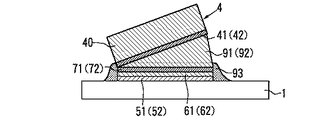
実施例1で調製したフラックスと、はんだ粉末とを混合し、はんだぺーストを調製した。はんだ粉末に対するフラックスの配合量は10wt%とした。このはんだペーストを用いて、チップ部品を部品搭載基板上にはんだ付けした。図4(a)〜(c)は部品搭載基板の詳細と、部品搭載基板に対するチップ部品のはんだ付け工程を示す部分断面図である。部品搭載基板1は、Cu膜51(52)、Ni膜61(62)及びAu膜71(72)を順次に積層して形成した2つのランドを有する。
【0039】
上述した部品搭載基板1のランドの上に、本発明に係るはんだペースト81(82)を塗布した(図4(a)参照)。はんだペースト81(82)の塗布に当たっては、厚み100μmのメタルマスクを用いて印刷した。メタルマスクの開口寸法は0.5mm×0.3mmとし、電子部品4の搭載されるランド寸法と同寸法とした。
【0040】
そして、はんだペースト81(82)の上に、長さ1mm、幅0.5mmの電子部品4を搭載(図4(b)参照)し、リフロー炉に通炉することにより、電子部品4を部品搭載基板1上にはんだ付けした(図4(c)参照)。これにより、本発明に係る電子部品装置が得られる。
【0041】
この後、図2に示した方法に従って横押し強度を測定した。図4(c)において、参照符号3は、はんだペースト81(82)に含まれていた本発明に係るフラックスを示し、端部電極41、42の外側でフィレット状になる。
【0042】
比較例2
比較のため、従来のロジン系フラックスを含むはんだペーストを用い、チップ部品を部品搭載基板にはんだ付けした。はんだ粉末に対するロジン系フラックスの配合量は10wt%とした。
【0043】
図5(a)〜(c)は部品搭載基板の詳細と、部品搭載基板に対するチップ部品のはんだ付け工程を示す部分断面図である。図示するように、部品搭載基板1は、Cu膜51(52)、Ni膜61(62)及びAu膜71(72)を順次に積層した2つのランドを有する。この部品搭載基板1のランドの上に、ロジン系フラックスを含有するはんだペースト91(92)を塗布した(図5(a)参照)。
【0044】
そして、ロジン系フラックスを含有するはんだペースト91(92)の上に、長さ1mm、幅0.5mmの電子部品4を搭載(図5(b)参照)し、リフロー炉に通炉することにより、電子部品4を部品搭載基板1上にはんだ付けした(図5(c)参照)。この後、図2に示した方法に従って、部品横押し強度を測定した。
【0045】
図6は実施例2及び比較例2の部品横押し強度試験の結果を示す図である。図示するように、比較例2の横押し強度の平均値は600g程度であったが、実施例2では平均値1500g程度の強度を得ることができた。
【0046】
実施例3
実施例1で調製したフラックスと、はんだ粉末とを混合し、はんだぺ一ストを調製した。はんだ粉末に対するフラックスの配合量は、20〜45wt%まで増やした。
【0047】
このはんだぺ一ストを用い、図7に従って、電子部品4を部品搭載基板1に搭載し、はんだ付けした。図7を参照して具体的に述べると、部品搭載基板1は、Cu膜51(52)、Ni膜61(62)及びAu膜71(72)を順次に積層して形成した2つのランドを有する(図7(a)参照)。
【0048】
上述した部品搭載基板1のランドの上に、本発明に係るはんだペースト81(82)を塗布した(図7(a)参照)。はんだペースト81(82)の塗布に当たっては、厚み100μmのメタルマスクを用いて印刷した。メタルマスクの開口寸法は0.5mm×0.3mmとし、電子部品4の搭載されるランド寸法と同寸法とした。
【0049】
そして、はんだペースト81(82)の上に、長さ1mm、幅0.5mmの電子部品4を搭載(図7(b)参照)し、リフロー炉に通炉することにより、電子部品4を部品搭載基板1上にはんだ付けした(図7(c)参照)。これにより、本発明に係る電子部品装置が得られる。
【0050】
はんだ付け後の外観は、図8に示す通りである。図8は図7(c)の8ー8線に沿った断面図である。実施例3では、意図的にフラックス含有量を増やしたはんだぺ一ストを用いたものであるが、実質、はんだ量が少なくて済み、電子部品4は、図8に示すように、傾斜することなく、正常な状態ではんだ付けされた。図7(c)及び図10において、参照符号3は、はんだペースト81(82)に含まれていた本発明に係るフラックスを示し、端部電極41、42の外側でフィレット状になる。
【0051】
また、本発明に係るフラックスを含有するはんだペーストを用いたことにより、はんだ付け後の電子部品4の周辺を、フラックスが覆い、部品横押し強度の向上も認められた。このように、はんだぺ一スト中のフラックス含有率を故意に向上させることにより、はんだ厚みを、はんだぺ一ストによって制御も可能となる。特に、フラックスの含有量が35wt%以上の領域で、斜めはんだ付けを回避し、かつ、従来品と同等以上の接合強度を得ることができた。
【0052】
比較例3
比較のために、従来のロジン系フラックス含有のはんだペーストを用い、図9に従って、電子部品4を部品搭載基板1に搭載し、はんだ付けした。図9を参照して具体的に述べると、部品搭載基板1は、Cu膜51(52)、Ni膜61(62)及びAu膜71(72)を順次に積層して形成した2つのランドを有する(図9(a)参照)。
【0053】
上述した部品搭載基板1のランドの上に、ロジン系フラックス含有のはんだペースト91(92)を塗布した(図9(a)参照)。はんだペースト91(92)の塗布に当たっては、厚み100μmのメタルマスクを用いて印刷した。メタルマスクの開口寸法は0.5mm×0.3mmとし、電子部品4の搭載されるランド寸法と同寸法とした。
【0054】
そして、はんだペースト91(92)の上に、長さ1mm、幅0.5mmの電子部品4を搭載(図9(b)参照)し、リフロー炉に通炉することにより、電子部品4を部品搭載基板1上にはんだ付けした(図9(c)参照)。
【0055】
リフローはんだ付け後の外観は、図10に示す通りである。図10は図9(c)の10ー10線に沿った部分断面図である。図10に示すように、従来のロジン系フラックス含有はんだぺ一ストではんだ付けしたものは、はんだ量が多すぎ、電子部品4が斜めにはんだ付けされた。図9(c)及び図10において、参照符号93は、はんだペースト91(92)に含まれていたロジン系フラックスを示す。
【0056】
実施例4
フラックスの配合組成について検討した。接着性樹脂として、液状エポキシ樹脂を用い、硬化剤としてアビエチン酸(カルボン酸)を用いた。液状エポキシ樹脂に対し、アビエチン酸を、表1に示す重量比で配合した。このフラックスを基板上に塗布し、230℃のリフロー炉に通炉し、樹脂硬化膜について検証した。

表1に示すように、液状エポキシ樹脂1wt%に対し、アビエチン酸1wt%の配合比のとき、硬い硬化膜となり、最も良好な結果が得られる。その他の配合比では、硬化しなかったり、ゲル状になったり、あるいは弾性硬化膜になったりするので、適当でない。リフロー温度に対しては、エポキシ樹脂の配合比、或いは、エポキシ樹脂の分子量、官能基数を変え、硬化剤(カルボン酸)の種類を検討すれば、任意の温度で、所望の硬化膜(接着性)を得ることができる。
【0058】
実施例5
実施例4で調製したフラックスと、はんだ粉末とを混合し、はんだペーストを調製した。はんだ粉末としては、Sn(96.5)Ag(3.5)を用いた。フラックスの含有量は25wt%とした。これを実施例5とする。
【0059】
図11は実施例5のはんだペーストを用いてチップ部品をはんだ付けした場合、及び、従来のロジン系はんだペーストを用いてチップ部品をはんだ付けした場合について、リフロー温度と部品横押し強度との関係を示す図である。図において、曲線L1は実施例5のはんだペーストを用いた場合の特性、曲線L2は従来のロジン系はんだペーストを用いた場合の特性である。
【0060】
図11に示すように、フラックスを含有するはんだぺ一ストは、220〜260℃のリフロー温度範囲において、従来のロジン系はんだペーストよりも高い接合強度を示す。特に、リフロー温度230℃以上で高い接合強度を確保することができた。
【0061】
実施例6
実施例5に示したはんだペーストを用いて、チップ部品を部品搭載基板にはんだ付けし、本発明に係る電子部品装置を得た。この後、部品搭載基板とチップ部品の端子極の接合性について観察したところ、フラックスを含有するはんだペーストは、ロジン系はんだペーストと同様の接合性を有していた。因に、従来の導電性接着剤や異方性導電ぺ一ストを上記フラックスと同様に評価した場合、部品搭載基板と部品の端子との接合は得られなかった。
【0062】
上記実施例では、部品搭載基板1の一面に電子部品4を搭載する例を示したが、部品搭載基板1の両面に電子部品4を搭載することができる。この場合、部品搭載基板1の一面上に、本発明に係るはんだペーストによるはんだ付け処理を実行した後、部品搭載基板1の他面上で、本発明に係るはんだペーストとは異なるはんだ、例えば、従来のロジン系はんだペーストを用いて、電子部品4をはんだ付けすることができる。これとは異なって、部品搭載基板1の両面側において、本発明に係るはんだペーストを用いて、電子部品4をはんだ付けすることもできる。何れの場合も、電子部品4がシフティング、マンハッタン現象(部品立ち現象)または脱落等の不具合を起こすことはない。
【0063】
<電子回路モジュール>
本発明に係る電子回路モジュールは、既に述べた電子部品装置との対比において、電子部品が、半導体チップに置き換わる点、及び、部品搭載基板がチップ搭載基板に置き換わる点を除けば、本質的に異なる点はない。換言すれば、本発明に係る電子回路モジュールの基本構成は、実質的に、電子部品装置に開示されている。用いられる半導体チップには、特に限定はない。半導体チップには、一般には、半導体素子(図示しない)または受動回路素子が含まれる。チップサイズパッケージ(CSP)と称される電子回路モジュールも、当然用いることができる。
【0064】
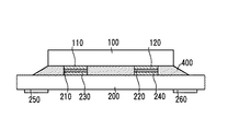
図12は本発明に係る電子回路モジュールの正面部分断面図である。図示された電子回路モジュールは、半導体チップ100と、チップ搭載基板200と、はんだ付け用フラックス400とを含む。図示された半導体チップ100は、下面等の適当な位置に、適当数の端子電極110、120が形成してあって、この端子電極110、120を、はんだ210、220によって、チップ搭載基板200の上のランド230、240に接合してある。
【0065】
チップ搭載基板200は、セラミック基板、有機樹脂基板またはそれらの組み合わせによって構成することができる。チップ搭載基板200の内部には、一般に、単層または複数層の導体パターン、及び、厚み方向に設けられたビヤホール等が形成されている。導体パターンは、単に、回路引き回しのために備えられる他、キャパシタまたはインダクタ等を構成するために備えられることもある。
【0066】
はんだ付け用フラックス400は、接着性樹脂と、硬化剤とを含有し、半導体チップ100と、チップ搭載基板200との間に介在し、両者を接着している。はんだ付け用フラックス400は接着剤として機能する。
【0067】
図示実施例において、はんだ付け用フラックス400は、半導体チップ100とチップ搭載基板200との間の隙間を、ほぼ埋めるように充填されている。
【0068】
既に述べたように、はんだ付け用フラックス400は洗浄する必要がなく、そのまま接着剤として用いることができる。従って、フラックス洗浄工程を必要とせず、製造コストの安価な電子回路モジュールを得ることができる。しかも、はんだ付け用フラックスは、接着性樹脂と、硬化剤とを含有しており、接着剤として機能するから、はんだ接合寿命を、従来よりも著しく長期化させた高信頼度の電子回路モジュールを得ることができる。
【0069】
図13は図12に示したCSP(チップサイズパッケ−ジ)等の電子回路モジュールのはんだ付け方法を説明する図である。このはんだ付け方法は、図1に示したはんだ付け方法を、電子回路モジュールのはんだ付けに適用したものに相当する。既に述べたように、接着性樹脂と、硬化剤とを含有するフラックス400を、予め、はんだバンプ210、220を形成したチップ搭載基板200の上に塗布する。はんだバンプ210、220はチップ搭載基板200の表面に設けられたランド230、240の上に形成されている。フラックス400の詳細は、既に述べた通りである。
【0070】
そして、このチップ搭載基板200の上に半導体チップ100を搭載する。半導体チップ100は、端子電極110、120がはんだバンプ210、220上に位置するようにして、チップ搭載基板200上に配置する。その後、半導体チップ100を搭載したチップ搭載基板200を、リフロー炉に通炉し、半導体チップ100の基体40の両端に設けられた端子電極110、120をはんだバンプ210、220にはんだ接合する。これにより、図12に示した電子回路モジュールが得られる。
【0071】
図14は本発明に係る電子回路モジュールの別の例を示す正面部分断面図である。図において、図12に図示された構成部分と同一の構成部分には、同一の参照符号を付してある。図示実施例において、はんだ付け用フラックス400は、半導体チップ100とチップ搭載基板200との間に介在し、はんだバンプ210、220の周りで、両者を接着している。
【0072】
この場合も、はんだ付け用フラックス400は洗浄する必要がなく、そのまま接着剤として用いることができる。従って、フラックス洗浄工程を必要とせず、製造コストの安価な電子回路モジュールを得ることができる。しかも、はんだ付け用フラックスは、接着性樹脂と、硬化剤とを含有しており、接着剤として機能するから、はんだ接合寿命を、従来よりも著しく長期化させた高信頼度の電子回路モジュールを得ることができる。
【0073】
図15は図14に示した電子回路モジュールのはんだ付け方法を説明する図である。このはんだ付け方法は、図4〜8に示したはんだ付け方法を、電子回路モジュールのはんだ付けに適用したものに相当する。既に述べた組成のはんだ粉末含有フラックス410、420を、予め、チップ搭載基板200の表面に設けられたランド230、240の上に塗布する。
【0074】
そして、このチップ搭載基板200の上に半導体チップ100を搭載する。半導体チップ100は、端子電極110、120がはんだ粉末含有フラックス410、420上に位置するようにして、チップ搭載基板200上に配置する。半導体チップ100を搭載したチップ搭載基板200を、リフロー炉に通炉し、半導体チップ100の両端に設けられた端子電極110、120をはんだ粉末含有フラックス410、420に含まれるはんだ成分によりはんだ接合する。
【0075】
接合状態では、はんだ粉末含有フラックス410、420に含まれる接着性樹脂及び硬化剤が、半導体チップ100とチップ搭載基板200との間に介在し、はんだバンプ210、220の周りで、両者を接着する。これにより、図14に示した電子回路モジュールが得られる。図15において、はんだ粉末含有フラックス410、420の量を増加させることにより、図12に図示したように、はんだ付け用フラックス400が、半導体チップ100とチップ搭載基板200との間の隙間を、ほぼ埋めるように充填した構造を実現することもできる。
【0076】
次に具体的な実施例及び比較例を挙げて説明する。
【0077】
実施例7
まず、次の組成になる熱硬化性フラックス入りのはんだぺ一ストを調製した。
【0078】
フラックス:ビスフエノールA樹脂/無水フタル酸を質量比1対1で混合し、溶剤を10質量%添加したもの
はんだ粉末:Sn−3.5Ag
上記はんだ粉末に対し、上記フラックスを、10質量%の割合で添加した。はんだ粉末の組成はリフロー温度に応じて選択できるもので、他の組成系でもよい。また、フラックスの配合量も任意に選択できる。
【0079】
上述した熱硬化性フラックス入りのはんだぺ一ストを、スクリーン印刷法により、有機系チップ搭載基板上に塗布した。スクリーン印刷に当たっては、メタルマスタ厚み100μmのスクリーンを用いた。
【0080】
次に、予め、はんだバンプが形成されている半導体チップを有機系チップ搭載基板上に載せ、リフロー炉に通炉した。リフロー温度は、最高温度240℃とし、220℃以上の通炉時間を30秒とした。
【0081】
比較例7
比較のため、封止剤を用いた従来品、および、封止剤を用いない従来品を用意した。
【0082】
<試験>
実施例7に係る電子回路モジュール、及び、2種の従来電子回路モジュールを熱衝撃試験に付した。熱衝撃試験は、(一55℃)を0.5時間保持し、次に(+125℃)を0.5時間保持し、これを1サイクルとし、2000サイクルまで行った。その後に、はんだ接続部分における直流抵抗(RDC)を測定した。
【0083】
図16はRDC測定結果を示すグラフである。図16において、横軸に熱衝撃サイクル(サイクル)を採り、縦軸にRDC(Ω)を採ってある。特性L11は封止剤を用いない従来品の特性、特性L12は封止剤を用いた従来品の特性、特性L13は本発明に係る実施例7の特性である。
【0084】
図16において、封止剤を用いなかった従来品は、特性L11で示されているように、1500サイクルを越えると、RDCが急激に増大しており、RDCが劣化している。これに対して、本発明に係る実施例7は、特性L13で示されるように、2000サイクルを経過してもRDCの劣化は見られなかった。これは、封止剤を用いた従来品の特性L12と同等の特性である。
【0085】
<電子回路装置>
本発明係る電子回路装置は、既に述べた電子部品装置との対比において、電子部品が、電子回路モジュールに置き換わる点、及び、部品搭載基板がマザー基板に置き換わる点を除けば、本質的に異なる点はない。換言すれば、本発明に係る電子回路装置の基本構成は、実質的に、電子部品装置に開示されている。
【0086】
図17は本発明に係る電子回路装置の正面部分断面図である。図示された電子回路装置は、電子回路モジュール300と、マザー基板500と、はんだ付け用フラックス600とを含む。
【0087】
電子回路モジュール300は、従来タイプの電子回路モジュールを用いることもできるが、好ましくは、図12、14に示した構造のものを用いる。電子回路モジュール300は、下面等の適当な位置に、適当数の端子電極250、260が形成してあって、この端子電極250、260を、はんだバンプ510、520によって、マザー基板500の上のランド530、540に接合してある。
【0088】
マザー基板200は、セラミック基板、有機樹脂基板またはそれらの組み合わせによって構成することができる。マザー基板500の内部には、単層または複数層の導体パターン、及び、厚み方向に設けられたビヤホール等が形成されることがある。導体パターンは、単に、回路引き回しのために備えられる他、キャパシタまたはインダクタ等を構成するために備えられることもある。
【0089】
はんだ付け用フラックス600は、接着性樹脂と、硬化剤とを含有し、電子回路モジュール300と、マザー基板500との間に介在し、両者を接着している。はんだ付け用フラックス600は、接着剤として機能する。図示実施例において、はんだ付け用フラックス600は、電子回路モジュール300とマザー基板500との間の隙間を、ほぼ埋めるように充填されている。
【0090】
はんだ付け用フラックス600は洗浄する必要がなく、そのまま接着剤として用いることができる。従って、フラックス洗浄工程を必要とせず、製造コストの安価な電子回路装置を得ることができる。しかも、はんだ付け用フラックスは、接着性樹脂と、硬化剤とを含有しており、接着剤として機能するから、はんだ接合寿命を、従来よりも著しく長期化させた高信頼度の電子回路装置を得ることができる。
【0091】
図18は図17に示した電子回路装置のはんだ付け方法を説明する図である。このはんだ付け方法は、図1に示したはんだ付け方法を、電子回路装置のはんだ付けに適用したものに相当する。既に述べたように、接着性樹脂と、硬化剤とを含有するフラックス600を、予め、はんだバンプ510、520を形成したマザー基板500の上に塗布する。フラックス600ははんだ粉末を含有しない。
【0092】
はんだバンプ510、520はマザー基板500の表面に設けられたランド530、540の上に形成されている。そして、このマザー基板500の上に電子回路モジュール300を搭載する。電子回路モジュール300は、端子電極250、260がはんだバンプ510、520上に位置するようにして、マザー基板500上に配置する。電子回路モジュール300を搭載したマザー基板500を、リフロー炉に通炉し、電子回路モジュール300の端子電極250、260をはんだバンプ510、520にはんだ接合する。これにより、図17に示した電子回路装置が得られる。
【0093】
図19は本発明に係る電子回路装置の別の例を示す正面部分断面図である。図において、図17に図示された構成部分と同一の構成部分には、同一の参照符号を付してある。図示実施例において、はんだ付け用フラックス600は、電子回路モジュール300とマザー基板500との間に介在し、はんだバンプ510、520の周りで、両者を接着している。
【0094】
この場合も、はんだ付け用フラックス600は洗浄する必要がなく、そのまま接着剤として用いることができる。従って、フラックス洗浄工程を必要とせず、製造コストの安価な電子回路装置を得ることができる。しかも、はんだ付け用フラックス600は、はんだ粉末を含む他、接着性樹脂と、硬化剤とを含有しており、接着剤として機能するから、はんだ接合寿命を、従来よりも著しく長期化させた高信頼度の電子回路装置を得ることができる。
【0095】
図20は図19に示した電子回路装置のはんだ付け方法を説明する図である。このはんだ付け方法は、図4〜8に示したはんだ付け方法を、電子回路装置のはんだ付けに適用したものに相当する。既に述べた組成にて調製したはんだ粉末含有フラックス610、620を、予め、マザー基板500の表面に設けられたランド530、540の上に塗布する。そして、このマザー基板500の上に電子回路モジュール300を搭載する。電子回路モジュール300は、端子電極250、260がはんだ粉末含有フラックス610、620上に位置するようにして、マザー基板500上に配置する。
【0096】
次に、電子回路モジュール300を搭載したマザー基板500を、リフロー炉に通炉し、電子回路モジュール300に設けられた端子電極250、260をはんだ粉末含有フラックス610、620に含まれるはんだ成分によりはんだ接合する。はんだ粉末含有フラックス610、620に含まれる接着性樹脂及び硬化剤が、電子回路モジュール300とマザー基板500との間に介在し、はんだバンプ510、520の周りで、両者を接着する。これにより、図19に示した電子回路装置が得られる。図20において、はんだ粉末含有フラックス610、620の量を増加させることにより、図17に図示したように、はんだ付け用フラックス600が、電子回路モジュール300とマザー基板500との間の隙間を、ほぼ埋めるように充填した構造を実現することもできる。
【0097】
次に具体的な実施例を挙げて説明する。
【0098】
実施例8
まず、次の組成になる熱硬化性フラックス入りのはんだぺ一ストを調製した。
【0099】
フラックス:ビスフエノールA樹脂/無水フタル酸を質量比1対1で混合し、溶剤を10質量%添加したもの
はんだ粉末:Sn−3.5Ag
上記はんだ粉末に対し、上記フラックスを、10質量%の割合で添加した。はんだ粉末の組成はリフロー温度に応じて選択できるもので、他の組成系でもよい。また、フラックスの配合量も任意に選択できる。
【0100】
マザー基板としては、有機系マザー基板を用いた。電子回路モジュールは、有機系のチップ搭載基板を用い、その上に半導体チップを搭載したものを用いた。有機系チップ搭載基板の下面に備えられた端子電極の表面には、有機系マザー基板とはんだ付けが可能なように、Auめっき処理を施した。
【0101】
上述した熱硬化性フラックス入りのはんだぺ一ストを、スクリーン印刷法により、有機系チップ搭載基板上に塗布した。スクリーン印刷に当たっては、メタルマスタ厚み100μmのスクリーンを用いた。
【0102】
次に、電子回路モジュールを、有機系マザー基板上に載せ、リフロー炉に通炉した。リフロー温度は、最高温度240℃とし、220℃以上の通炉時間を30秒とした。
【0103】
実施例9
電子回路モジュールのチップ搭載基板を、セラミック基板とした他は、実施例8と同様にして、電子回路装置を製造した。
【0104】
比較例8
電子回路モジュールのチップ搭載基板を有機系材料によって構成し、この電子回路モジュールを、従来のフラックスを用いて、有機系マザー基板にはんだ付けした。有機系チップ搭載基板の下面に備えられた端子電極の表面には、有機系マザー基板とはんだ付けが可能なように、Auめっき処理を施した。
【0105】
比較例9
電子回路モジュールのチップ搭載基板をセラミック材料によって構成し、この電子回路モジュールを、従来のフラックスを用いて、有機系マザー基板にはんだ付けした。セラミック系チップ搭載基板の下面に備えられた端子電極の表面には、有機系マザー基板とはんだ付けが可能なように、Auめっき処理を施した。
【0106】
<試験>
実施例8、9に係る電子回路モジュール、及び、比較例8、9に係る従来電子回路モジュールを熱衝撃試験に付した。熱衝撃試験は、(一55℃)を0.5時間保持し、次に(+125℃)を0.5時間保持し、これを1サイクルとし、2000サイクルまで行った。その後に、はんだ接続部分における直流抵抗(RDC)を測定した。
【0107】
図21はRDC測定結果を示すグラフである。図21において、横軸に熱衝撃サイクル(サイクル)を採り、縦軸にRDC(Ω)を採ってある。特性L21は比較例9の特性、特性L22は実施例8、9及び比較例8の特性である。
【0108】
図21において、電子回路モジュールのチップ搭載基板がセラミック材料でなり、マザー基板が有機材料でなる比較例9は、特性L21で示されているように、1000サイクルを越えると、RDCが急激に増大し、RDCが劣化する。これに対して、本発明に係る実施例8、9は、特性L22で示されるように、2000サイクルを経過してもRDCの劣化は見られなかった。特に、実施例9の特性L22と、比較例9の特性L21との対比から明らかなように、電子回路モジュールのチップ搭載基板を、セラミック基板とし、マザー基板を有機樹脂基板とした場合、従来は著しいRDCの劣化を招いていた(特性L21参照)が、本発明によれば、このような基板の組み合わせにおいても、RDCの劣化を阻止できる(特性L22参照)という優れた効果が得られる。
【0109】
上述したように、本発明では、フラックスに含まれる接着性樹脂を利用して、電子部品を部品搭載基板に接着する。この後、電子部品と部品搭載基板とが接着された状態で、はんだ付けの状態を検査する検査工程に付される。はんだ付け不良の場合、部品搭載基板から電子部品を取り外し、その電子部品を、再度、部品搭載基板にはんだ付けしたい。もし、部品搭載基板から電子部品を取り外すことができないならば、電子部品及び部品搭載基板は、廃棄することになり、コストの増大または歩留まりの低下を招く。そこで、本発明のフラックス及びはんだペーストは、はんだ付けの後で部品搭載基板から電子部品を取り外すことのできるものであることが好ましい。
【0110】
また、最近、地球環境保全の立場から、Pbを含有しないはんだ(Pbフリーはんだ)が導入されつつあり、様々な組成のはんだ成分が利用されるようになっている。はんだ成分は、その組成により、融点が異なるので、利用するはんだ成分の組成に応じて、様々な値のリフロー温度を設定しなければならない。このため、設定される任意のリフロー温度に応じて接着性樹脂を硬化できる技術が必要である。
【0111】
ここでは、電子部品を、部品搭載基板にはんだ付けする場合を例にとって説明したが、半導体チップをチップ搭載基板にはんだ付けする場合、及び、電子回路モジュールをマザー基板にはんだ付けする場合も同様である。
【0112】
次に、上述した問題点を解決するフラックス及びはんだペーストの構成を開示する。まず、フラックスにおいて、硬化剤は、少なくとも2種のカルボン酸を含み、これらのカルボン酸は、互いに異なる融点を有する。融点の低いカルボン酸は、リフロー温度で硬化剤として機能する。また、融点の高いカルボン酸は、リフロー温度より高いリペア温度で接着性樹脂の粘度を低下させる。
【0113】
フラックスの温度を、リペア温度前後に上昇させると、融点の高いカルボン酸も溶融し、接着性樹脂の粘度が低下するので、部品搭載基板から電子部品を取り外すことができる。従って、接着機能を保持しながら、従来のロジンフラックスと同様に電子部品をリペアすることができる。このような組成の接着性フラックスは、電子回路モジュール等の高価な大型パッケージ品をはんだ付けする場合、特に有益である。
【0114】
しかも、互いに融点の異なるカルボン酸を混合することにより、接着性樹脂の熱硬化温度を変えることができる。従って、任意のリフロー温度で接着性樹脂を硬化できるようになり、利用するはんだ成分の融点に合わせてリフロー温度を変更できるようになる。
【0115】
更に、混合するカルボン酸の組み合わせまたは混合比を変更することによっても、接着性樹脂の熱硬化温度を変えることができ、同様な作用及び効果が得られる。
【0116】
次に、はんだペーストは、上述の構成のフラックスと、はんだ粉末とを含む。従って、このはんだペーストも、上述の構成のフラックスと同様な作用及び効果を得られる。
【0117】
上述した作用及び効果を、実験を参照して具体的に説明する。まず、リペア性に優れたフラックス及びはんだペーストを得るため、次のような実験1を行った。
【0118】
実験1:複数種のカルボン酸の組み合わせによるリペア性の獲得
熱硬化性樹脂としてビスフェノールAを用いた。硬化剤としては、2種類のカルボン酸、具体的には、アジピン酸とピメリット酸とを用いた。アジピン酸及びピメリット酸はカルボン酸の範疇に含まれる。アジピン酸とピメリット酸とは、融点が互いに異なる。具体的には、アジピン酸の融点は153℃、ピメリット酸の融点は279℃である。ビスフェノールAとアジピン酸とピメリット酸とを、下記の表2に示す配合比(質量%)で配合し、サンプル1〜4のフラックスを調製した。サンプル1〜4のフラックスは、アジピン酸の含有率をa(質量%)とし、ピメリット酸の含有率をb(質量%)としたとき、
a:b=(50:50)〜(95:5)(但しa+b=100)
の範囲で変化させてある。また、ビスフェノールAとアジピン酸とを、下記の表2に示す配合比(質量%)で配合し、サンプル5のフラックスを調製した。
次に、調製した各サンプル1〜5のフラックスに、はんだ粉末を混合し、はんだペーストを調製した。はんだ粉末としてはSn−3.5Agを用いた。はんだ粉末の組成はリフロー温度に応じて選択できるもので、他の組成系でもよい。また、はんだ粉末に対するフラックスの配合量は25質量%とした。フラックスの配合量も任意に選択できる。
【0120】
上記組成において製作したはんだぺ一ストを用いて、マザー基板上に電子回路モジュールをはんだ付けした。図22〜図25は、マザー基板に対する電子回路モジュールのはんだ付け工程を示す正面部分断面図である。図において、図19に図示された構成部分と同一の構成部分には、同一の参照符号を付してある。
【0121】
図22に示すように、マザー基板500の表面には、ランド530、540が設けられている。マザー基板500は、セラミック基板、有機樹脂基板またはそれらの組み合わせによって構成することができる。図示のマザー基板500は、有機樹脂基板でなる。
【0122】
図23に示すように、マザー基板500のランド530、540の上に、実施例10のはんだペースト610、620を塗布した。はんだペースト610、620の塗布に当たっては、メタルマスクを用いて印刷した。
【0123】
そして、図24に示すように、マザー基板500の上に電子回路モジュール300を搭載した。図示の電子回路モジュール300は、図12に図示された電子回路モジュールと同様な構成である。電子回路モジュール300は、LGA構造品と称されるCSP(チップサイズパッケージ)の電子回路モジュールである。電子回路モジュール300のチップ搭載基板200はセラミック基板でなる。図24に示すように、電子回路モジュール300は、端子電極250、260がはんだペースト610、620上に位置するようにして、マザー基板500上に配置した。
【0124】
次に、電子回路モジュール300を搭載したマザー基板500を、リフロー炉に通炉し、電子回路モジュール300に設けられた端子電極250、260をはんだペースト610、620に含まれるはんだ成分によりはんだ接合した。はんだペースト610、620に含まれる接着性樹脂及び硬化剤が、電子回路モジュール300とマザー基板500との間に介在し、はんだバンプ510、520の周りで、両者を接着する。これにより、図25に示すように、本発明に係る電子回路装置が得られる。図25において、参照符号600は、はんだペースト610(620)に含まれていた実施例10のフラックスを示し、端子電極250、260の外側でフィレット状になる。
【0125】
上述したように、フラックス600は、接着性樹脂と、硬化剤とを含んでいる。硬化剤は、アジピン酸と、ピメリット酸とを含み、アジピン酸と、ピメリット酸は、互いに異なる融点を有する。融点の低いアジピン酸は、リフロー温度で硬化剤として機能する。融点の高いピメリット酸は、リフロー温度より高いリペア温度で接着性樹脂の粘度を低下させる。
【0126】
以下、具体的に、サンプル1〜5のフラックスについて述べる。サンプル5のフラックスを用いた場合、リフロー炉に通炉することにより、フラックスに含まれるアジピン酸が溶融し、はんだが溶融した。この結果、マザー基板のランドと、電子回路モジュールの端子電極とが接合された。
【0127】
サンプル1、2のフラックスを用いた場合、リフロー炉に通炉しても、フラックスに含まれるピメリット酸の硬化が進行し、はんだが溶融しなかった。このため、マザー基板のランドと電子回路モジュールの端子電極とが接合されなかった。
【0128】
サンプル3、4のフラックスを用いた場合、リフロー炉に通炉することにより、フラックス600に含まれるアジピン酸が溶融し、はんだが溶融した。この結果、マザー基板500のランド530、540と、電子回路モジュール300の端子電極250、260とが接合された。
【0129】
図26、図27は、マザー基板から電子回路モジュールを取り外す工程を示す正面部分断面図である。図26に示すようにフラックス600に熱風を吹き込み、フラックス600の温度を、リペア温度前後に上昇させると、融点の高いピメリット酸が溶融し、接着性樹脂の粘度が低下する。このため、図27に示すように、マザー基板500から電子回路モジュール300を取り外すことができる。
【0130】
従って、接着機能を保持しながら、従来のロジンフラックスと同様に電子回路モジュール300をリペアすることができる。かような組成の接着性フラックスは、大型パッケージ等の高価な電子回路モジュール300をはんだ付けする場合、特に有効である。また、この接着性フラックスのリペア工法は、従来はんだ付けのリペア工法と同じ作業レベルで実行できる。
【0131】
以下、具体的に述べる。サンプル1〜5のフラックスのうち、リフロー実装できたサンプル3〜5のフラックスに対してリペア実験を行った。リペア実験では、電子回路モジュール300のチップ搭載基板200と、マザー基板500との接合部に300℃前後の熱風を吹き込んだ。
【0132】
サンプル5のフラックスは、電子回路モジュールのチップ搭載基板と、マザー基板とを接着しており、一度軟化したが、熱風により再び硬化した。このため、マザー基板から電子回路モジュールを引き剥がすことはできなかった。
【0133】
サンプル3、4のフラックス600を用いた場合、電子回路モジュール300のチップ搭載基板200と、マザー基板500との接合部に熱風を吹き込むと、フラックス600に含まれるピメリット酸が再溶融し、マザー基板500から電子回路モジュール300を引き剥がすことができた。
【0134】
よって、はんだ付けされた電子回路モジュール300をリペアするためには、接着性樹脂硬化用のアジピン酸の他に、リペア温度付近に融点を有するピメリット酸を混合しておけばよい。リペア温度で、そのピメリット酸を溶融させると、接着性樹脂の粘度が低下する。このため、マザー基板500上にはんだ付けされた電子回路モジュール300を、マザー基板500から取り外し、リペアすることができる。
【0135】
上述した実験1の結果によれば、好ましくは、接着性樹脂硬化用のアジピン酸に、リペア用のピメリット酸を15質量%〜5質量%添加すればよい。言い換えれば、アジピン酸の含有率a(質量%)と、ピメリット酸の含有率b(質量%)とについて、
a:b=(85:15)〜(95:5)(但しa+b=100)
を満たせばよい。
【0136】
実験1で調製したフラックスは、はんだ粉末と混合され、混合により得られたはんだペーストを用いてはんだ付けを行っている。これと異なり、はんだバンプを施した基板上に実験1のフラックスを塗布してはんだ付けを行っても、同様な作用及び効果が得られる。
【0137】
本発明に係る電子部品装置は、既に述べた電子回路装置との対比において、電子回路モジュールが、電子部品に置き換わる点、及び、マザー基板が部品搭載基板に置き換わる点を除けば、本質的に異なる点はない。換言すれば、本発明に係る電子部品装置の基本構成は、実質的に、電子回路装置に開示されている。
【0138】
同様に、本発明に係る電子回路モジュールは、既に述べた電子回路装置との対比において、電子回路モジュールが、半導体チップに置き換わる点、及び、マザー基板がチップ搭載基板に置き換わる点を除けば、本質的に異なる点はない。換言すれば、本発明に係る電子回路モジュールの基本構成は、実質的に、電子回路装置に開示されている。
【0139】
次に、リフロー温度を変更するため、次のような実験2〜5を行った。まず、実験2では、硬化剤として一種のカルボン酸のみを配合してフラックスを調製し、フラックスの熱硬化物性を調べた。
【0140】
実験2:一種のカルボン酸のみを配合したフラックスの熱硬化物性
熱硬化性樹脂としてビスフェノールAを用いた。硬化剤としては、下記の表3に示すように、アジピン酸、マレイン酸、コハク酸またはピメリット酸の1つを用いた。熱硬化性樹脂と、上述の硬化剤とを質量比1:1の割合で配合し、フラックスを調製した。そして、調製したフラックスを2g、Cu板上に塗布し、240℃のリフロー炉に通炉し、皮膜の挙動を比較した。
表3に示すように、サンプル11、12のフラックスでは、皮膜が、ゲル化したり、常温で硬化したりするので適当でない。これらに対し、サンプル13、14のフラックスでは、皮膜がリフロー通炉により硬化し、良好な結果が得られた。
【0142】
サンプル11〜14のフラックスにおいて、硬化の進み具合を比較する。硬化剤の融点が高いと熱硬化が進み、アジピン酸を硬化剤としたフラックス(サンプル11)の硬化が最も遅い。硬化剤としてアジピン酸とコハク酸を混合した場合、コハク酸の配合比を増やすにつれ、より硬い硬化皮膜が得られる。
【0143】
上述の実験2を踏まえ、アジピン酸とコハク酸とを混合してリフロー温度の変更を試みた。
【0144】
実験3:複数種のカルボン酸の混合によるリフロー温度の変更
熱硬化性樹脂としてビスフェノールAを用いた。硬化剤としては、2種類のカルボン酸、具体的には、アジピン酸とコハク酸とを用いた。アジピン酸及びコハク酸はカルボン酸の範疇に含まれる。アジピン酸とコハク酸とは、融点が互いに異なる。具体的には、アジピン酸の融点は153℃、コハク酸の融点は188℃である。ビスフェノールAとアジピン酸とコハク酸とを、質量比1:0.5:0.5の割合で配合し、フラックスを調製した。
【0145】
次に、調製したフラックスと、はんだ粉末とを混合し、はんだペーストを調製した。はんだ粉末としてはSn−3.5Agを用い、はんだ粉末に対するフラックスの配合量は15質量%とした。以下、このはんだペーストを、サンプル22のはんだペーストと呼ぶ。はんだ粉末の組成はリフロー温度に応じて選択できるもので、他の組成系でもよい。フラックスの配合量も任意に選択できる。
【0146】
また、ビスフェノールAとアジピン酸とを、質量比1:1の割合で配合し、フラックスを調製した。そして、調製したフラックスと、はんだ粉末とを混合し、はんだペーストを調製した。サンプル22のはんだペーストと同様に、はんだ粉末としてはSn−3.5Agを用い、はんだ粉末に対するフラックスの配合量は15質量%とした。以下、このはんだペーストを、サンプル21のはんだペーストと呼ぶ。
【0147】
図28は、サンプル21、22のはんだペーストを用いてコンデンサをはんだ付けした場合について、リフロー温度と部品横押し強度との関係を示す図である。試験用のコンデンサとして、1005サイズのSTD端子コンデンサと、1005サイズのCSB端子コンデンサとの2種類を用いた。STD端子コンデンサとは、コンデンサ素体の両側面に端子を形成したコンデンサである。CSB端子コンデンサとは、コンデンサ素体の底面の両端に端子を形成したコンデンサである。
【0148】
図28において、特性L31はSTD端子コンデンサにサンプル21のはんだペーストを用いた場合の特性、特性L32はSTD端子コンデンサにサンプル22のはんだペーストを用いた場合の特性、特性L41はCSB端子コンデンサにサンプル21のはんだペーストを用いた場合の特性、特性L42はCSB端子コンデンサにサンプル22のはんだペーストを用いた場合の特性である。部品横押し強度は、前述の図2に示した方法に従って測定した。
【0149】
図28に示すように、STD端子コンデンサをはんだ付けする場合、サンプル22のはんだペースト(特性L32参照)は、サンプル21のはんだペースト(特性L31参照)よりも低いリフロ−温度で同程度の部品横押し強度を得られた。
【0150】
また、CSB端子コンデンサをはんだ付けする場合、サンプル22のはんだペースト(特性L42参照)は、サンプル21のはんだペースト(特性L41参照)よりも低いリフロ−温度で同程度の部品横押し強度を得られた。例えば、部品横押し強度として0.9kg必要であると仮定すると、サンプル21のはんだペースト(特性L41参照)の場合、224〜230℃のリフロ−温度を必要とするが、サンプル22のはんだペースト(特性L42参照)の場合、217〜221℃のリフロ−温度で済む。
【0151】
以上述べたように、互いに融点の異なるカルボン酸(アジピン酸とコハク酸)を混合することにより、接着性樹脂(ビスフェノールA)の熱硬化温度を変えることができる。従って、任意のリフロー温度で接着性樹脂(ビスフェノールA)を硬化できるようになり、利用するはんだ成分の融点に合わせてリフロー温度を変更できるようになる。リフロ−温度は一定の値に固定せずに済むようになる。
【0152】
更に、混合するカルボン酸の組み合わせ(アジピン酸及びコハク酸)を変更することによっても、接着性樹脂(ビスフェノールA)の熱硬化温度を変えることができ、同様な作用及び効果が得られる。例えば、アジピン酸とコハク酸との組み合わせを、アジピン酸とピメリット酸との組み合わせに変更すると、接着性樹脂(ビスフェノールA)の熱硬化温度が変わる。
【0153】
次に、混合するカルボン酸(アジピン酸とコハク酸)の混合比を調整して、リフロー温度の変更を試みた。
【0154】
実験4:カルボン酸の混合比の調整によるリフロー温度の変更
熱硬化性樹脂としてビスフェノールAを用いた。硬化剤としては、アジピン酸とコハク酸とを用いた。ビスフェノールAとアジピン酸とコハク酸とを、下記の表4に示す配合比(質量%)で配合し、フラックスを調製した。これらのフラックスは、アジピン酸の含有率をa(質量%)とし、コハク酸の含有率をc(質量%)としたとき、
a:c=(100:0)〜(0:100)(但しa+c=100)
の範囲で変化させてある。
【0155】
次に、調製した各フラックスにはんだ粉末を混合し、サンプル50〜55のはんだペーストを調製した。はんだ粉末としては、共晶はんだ(Sn63−Pb37)の粉末を用いた。はんだ粉末に対するフラックスの配合量は15質量%とした。はんだ粉末の組成はリフロー温度に応じて選択できるもので、他の組成系でもよい。フラックスの配合量も任意に選択できる。
表4に示すように、サンプル50のはんだペーストは、はんだ付けにおいて端子を良好に接続できた。しかし、サンプル50のはんだペーストは、硬化剤としてアジピン酸しか含んでいないので、接着性樹脂(ビスフェノールA)の熱硬化温度を変えることができず、リフロー温度を変更できない。
【0157】
また、サンプル55のはんだペーストは、はんだが溶融する前にフラックスが硬化してしまい、端子を接合できなかった。
【0158】
これに対し、サンプル51〜54のはんだペーストは、それぞれ、はんだ付けにおいて端子を良好に接続できた。
【0159】
図32は、サンプル50〜54のはんだペーストを用いてコンデンサをはんだ付けした場合について、リフロー温度と部品横押し強度との関係を示す図である。試験用のコンデンサとしては、1005サイズのSTD端子コンデンサを用いた。図29において、特性L50〜L54は、それぞれ、サンプル50〜54のはんだペーストを用いた場合の特性である。
【0160】
コハク酸の配合率を増大させることにより、低いリフロー温度でも、必要な部品横押し強度を確保することができる。例えば、部品横押し強度として1.4kg必要であると仮定すると、サンプル52のはんだペースト(特性L52参照)は、230℃のリフロ−温度を必要とする。これに対し、サンプル53のはんだペースト(特性L53参照)は、上述のサンプル52よりもコハク酸の配合率を増大させてあるので、210℃のリフロ−温度で済む。
【0161】
以上述べたように、混合するカルボン酸(アジピン酸とコハク酸)の混合比を変更することにより、接着性樹脂(ビスフェノールA)の熱硬化温度を変えることができる。従って、任意のリフロー温度で接着性樹脂(ビスフェノールA)を硬化できるようになり、利用するはんだ成分の融点に合わせてリフロー温度を変更できるようになる。リフロ−温度は一定の値に固定せずに済むようになる。
【0162】
上述した実験4の結果によれば、はんだ成分として共晶はんだ(Sn63−Pb37)を用いる場合、硬化剤としてアジピン酸及びコハク酸を配合するとき、アジピン酸の含有率a(質量%)と、コハク酸の含有率c(質量%)とについて、
a:c=(95:5)〜(25:75)(但しa+c=100)
を満たすのが好ましい。
【0163】
実験4では、はんだ成分として共晶はんだ(Sn63−Pb37)を用いている。共晶はんだ(Sn63−Pb37)の融点は183℃である。
【0164】
かような実験4と異なり、はんだ成分としてSn−3.5Agはんだを用いた実験(以下実験5と称する)を説明する。Sn−3.5Agはんだの融点は217℃であり、共晶はんだ(Sn63−Pb37)の融点183℃よりもかなり高い。
【0165】
実験5:フラックスと組み合わせられるはんだ成分の変更
ビスフェノールAとアジピン酸とコハク酸とを、下記の表5に示す配合比(質量%)で配合し、フラックスを調製した。これらのフラックスは、アジピン酸の含有率をa(質量%)とし、コハク酸の含有率をc(質量%)としたとき、
a:c=(100:0)〜(0:100)(但しa+c=100)
の範囲で変化させてある。
【0166】
次に、調製した各フラックスにはんだ粉末を混合し、サンプル70〜75のはんだペーストを調製した。はんだ粉末としては、Sn−3.5Agはんだ粉末を用いた。はんだ粉末に対するフラックスの配合量は15質量%とした。
表5に示すように、サンプル72〜75のはんだペーストは、それぞれ、はんだが溶融する前にフラックスが硬化してしまい、端子を接合できなかった。
【0168】
また、サンプル70、71のはんだペーストは、それぞれ、はんだ付けにおいて端子を良好に接続できた。
【0169】
上述した実験5の結果によれば、はんだ成分としてSn−3.5Agはんだを用いる場合、硬化剤としてアジピン酸及びコハク酸を配合するとき、アジピン酸の含有率a(質量%)と、コハク酸の含有率c(質量%)とについて、
a:c=(100:0)〜(95:5)(但しa+c=100)
を満たすのが好ましい。
【0170】
上述した実験3〜5では、フラックスを、はんだ粉末に混合し、混合により得られたはんだペーストを用いてはんだ付けを行っている。これと異なり、はんだバンプを施した基板上にフラックスを塗布してはんだ付けを行っても、同様な作用及び効果が得られる。
【0171】
実験3〜5で調製したはんだペーストを利用しても、図25に図示された電子回路装置と同様な電子回路装置を構成できることは自明である。勿論、実験3〜5のはんだペーストを利用して電子部品装置及び電子回路モジュールを構成することもできる。
【0172】
また、硬化剤として、互いに熱硬化速度の異なるカルボン酸を混合すると、接着性樹脂の熱硬化速度を変えることができる。従って、利用するはんだ成分に合わせてリフロー時間またはリフロー温度を変更できるようになる。例えば、アジピン酸とコハク酸の場合、コハク酸の熱硬化に必要な熱量は、アジピン酸の熱硬化に必要な熱量よりも少ないので、コハク酸の熱硬化速度は、アジピン酸の熱硬化速度よりも速い。従って、硬化剤としてアジピン酸とコハク酸とを混合すると、接着性樹脂(ビスフェノールA)の熱硬化速度を変更でき、リフロー時間またはリフロー温度を変更できる。他のカルボン酸の組み合わせ、例えば、アジピン酸とピメリット酸の場合も同様である。
【0173】
更に、混合するカルボン酸の組み合わせまたは混合比を変更することによっても、接着性樹脂の熱硬化速度を変えることができ、同様な作用及び効果が得られる。
【0174】
図示は省略するが、本発明に係るはんだペーストを用いる場合、本発明に係るフラックスを封止剤として用い、電子部品と部品搭載基板、半導体チップとチップ搭載基板及び電子回路モジュールとマザー基板とを、フラックスでなる封止剤によって接合することもできる。また、本発明に係るフラックスを用いた部品搭載基板において、本フラックスの上層部に一般的な封止剤を形成することもできる。
【0175】
【発明の効果】
以上述べたように、本発明によれば、次のような効果が得られる。
(a)実装の高密度化、部品の小型化及び部品の配置間隔の狭ピッチ化等に対しても、十分な接合強度をもって対応し得るはんだ付け用フラックス及びはんだペースト及びはんだ付け方法を提供することができる。
(b)両面実装タイプの部品搭載基板において、部品の浮動または脱落等の不具合を確実に阻止し得るはんだ付け用フラックス及びはんだペースト及びはんだ付け方法を提供することができる。
(c)フラックス洗浄工程を必要とせず、製造コストの安価な電子部品装置、電子回路モジュール及び電子回路装置を提供することができる。
(d)はんだ接合寿命を、従来よりも著しく長期化させた高信頼度の電子部品装置、電子回路モジュール及び電子回路装置を提供することができる。
【図面の簡単な説明】
【図1】本発明に係るフラックスを用いたチップ部品のはんだ付け方法を示す部分断面図である。
【図2】部品搭載基板にはんだ付けされたチップ部品の横押し強度試験方法を示す部分断面図である。
【図3】図2に示した部品横押し強度試験による結果を示す図である。
【図4】本発明に係るフラックスを含有するはんだペーストを用いた場合について、部品搭載基板の詳細と、部品搭載基板に対するチップ部品のはんだ付け工程を示す部分断面図である。
【図5】従来のロジン系フラックスを含有するはんだペーストを用いた場合について、部品搭載基板の詳細と、部品搭載基板に対するチップ部品のはんだ付け工程を示す部分断面図である。
【図6】図4に示す本発明に係るはんだ付け方法と、図5に示す従来のはんだ付け方法とについて、部品横押し強度試験の結果を示す図である。
【図7】本発明に係るフラックスを含有するはんだペーストを用いたはんだ付け方法を示す部分断面図である。
【図8】図7に示した本発明に係るはんだ付け方法によって、チップ部品を部品搭載基板上にはんだ付けした場合の外観を示す図であって、図7の8ー8線に沿った部分断面図である。
【図9】従来のロジン系フラックス含有のはんだペーストを用いたはんだ付け方法を示す部分断面図である。
【図10】図9に示した従来のはんだ付け方法によって、チップ部品を部品搭載基板上にはんだ付けした場合の外観を示す図であって、図9の10ー10線に沿った部分断面図である。
【図11】本発明に係るはんだペーストを用いてチップ部品をはんだ付けした場合と、従来のロジン系フラックス含有はんだペーストを用いてチップ部品をはんだ付けした場合のリフロー温度と部品横押し強度との関係を示す図である。
【図12】本発明に係る電子回路モジュールの正面部分断面図である。
【図13】図12に示した電子回路モジュールのはんだ付け方法を説明する図である。
【図14】本発明に係る電子回路モジュールの別の例を示す正面部分断面図である。
【図15】図14に示した電子回路モジュールのはんだ付け方法を説明する図である。
【図16】RDC測定結果を示すグラフである。
【図17】本発明に係る電子回路装置の正面部分断面図である。
【図18】図17に示した電子回路装置のはんだ付け方法を説明する図である。
【図19】本発明に係る電子回路装置の別の例を示す正面部分断面図である。
【図20】図19に示した電子回路装置のはんだ付け方法を説明する図である。
【図21】RDC測定結果を示すグラフである。
【図22】マザー基板に対する電子回路モジュールのはんだ付け工程を示す正面部分断面図である。
【図23】図22に示した工程の次の工程を示す正面部分断面図である。
【図24】図23に示した工程の次の工程を示す正面部分断面図である。
【図25】図24に示した工程の次の工程を示す正面部分断面図である。
【図26】マザー基板から電子回路モジュールを取り外す工程を示す正面部分断面図である。
【図27】図26に示した工程の次の工程を示す正面部分断面図である。
【図28】サンプル21、22のはんだペーストを用いてコンデンサをはんだ付けした場合について、リフロー温度と部品横押し強度との関係を示す図である。
【図29】サンプル50〜54のはんだペーストを用いてコンデンサをはんだ付けした場合について、リフロー温度と部品横押し強度との関係を示す図である。
【符号の説明】
1 部品搭載基板
21、22 はんだバンプ
3 フラックス
4 チップ部品
81、82 はんだペースト[0001]
BACKGROUND OF THE INVENTION
The present invention relates to a soldering flux, a solder paste, an electronic component device, an electronic circuit module, an electronic circuit device, and a soldering method.
[0002]
[Prior art]
For example, when soldering a component to a component mounting board, a flux is used as is well known. The main function of the flux is to improve the wettability of the solder by removing the metal conductor provided on the component mounting board and the oxide film on the surface of the soldering metal of the component. As the flux, one having rosin as a main component is best known. The rosin contains carboxylic acids such as abietic acid and levobimalic acid, and the oxide film on the metal surface to be soldered is removed by the action of the carboxyl group.
[0003]
In addition to the above-mentioned rosin, the flux is usually mixed with various additives such as a solvent, a plasticizer or a thixotropic agent for the purpose of improving printability and obtaining a temporary fixing strength. For example, Japanese Patent Application Laid-Open No. 11-121915 discloses a type of flux whose viscosity is adjusted by adding an alcohol.
[0004]
Further, as another flux, an RMA (halogen free) flux defined by the mill standard is also known. In the case of this flux, a cleaning process such as flux is omitted after reflow.
[0005]
The above-mentioned flux does not participate in the bonding of the soldered parts after soldering, and the solder joint is achieved by the solder joint of the solder metal. Therefore, the joint strength between the soldered metals depends on the solder joint area.
[0006]
However, as high-density mounting progresses in various electronic devices, the size of components has been reduced, and the spacing between components has been narrowed, and as a result, the solder joint area has been rapidly narrowing. However, it is already difficult to ensure sufficient soldering strength. In addition, mounting density, component miniaturization, and component placement interval narrowing tend to progress further, and conventional means of ensuring solder joint strength only by solder joint area responds to this technological trend. It tends to become increasingly difficult to do.
[0007]
In general, as means for securing solder joint strength, means for forming a solder fillet portion and expanding a solder joint area between a component terminal and a conductor (land or solder bump) on a component mounting board is employed. However, in high-density mounting, since the joint area of the fillet portion is also reduced, it is difficult to adopt means for increasing the joint strength by the fillet portion.
[0008]
In addition, for example, in various electronic circuit modules, a double-sided mounting type component mounting board is used. After soldering (furnace) the component on one side of the component mounting board using high-temperature solder, the component is mounted on the other side. Then pass the furnace again. Therefore, when soldering a component on the other surface side of the component mounting board, it is necessary to solder using a low temperature solder having a melting point lower than that of the high temperature solder on the one surface side. Conventionally, the melting point of solder has been generally adjusted by the content of Pb.
[0009]
However, from the standpoint of global environmental protection, solder containing no Pb (Pb-free solder) is required, and development of such a solder composition is actively performed. However, a Pb-free solder having a high-melting-point melting point comparable to conventional high-temperature solder has not been put into practical use at present. This is because the melting point of the Pb-free solder itself is about 220 ° C., which is about 40 ° C. higher than that of the eutectic solder, and no alternative composition other than Pb can be found. For this reason, in a component mounting board of a double-sided mounting type, the difference in melting point of the solder used on both sides cannot be taken sufficiently, and when the component is mounted on the component mounting board, the component floats or falls off, etc. The problem occurs.
[0010]
Furthermore, in an electronic circuit module using a semiconductor chip, after the semiconductor chip is soldered to the chip mounting substrate, a sealing agent is poured into the bonding interface, and the semiconductor chip and the chip mounting substrate are bonded and fixed with the sealing agent. Work is added.
[0011]
However, if a flux residue remains at the time of injection of the sealing agent, the sealing agent does not sufficiently reach the interface between the semiconductor chip and the substrate due to the flux, and the adhesive force cannot be exhibited. Therefore, a step of washing the flux is added before injecting the sealant. The cleaning of the flux is usually performed in several times using a volatile organic solvent. However, the use of a volatile organic solvent is restricted for the purpose of environmental protection and the like, and the flux cleaning process is a burdensome process in terms of both cost and environmental protection.
[0012]
Furthermore, when the electronic circuit module obtained as described above is mounted on a mother substrate to constitute an electronic circuit device, in a combination using ceramic for the chip mounting substrate and using an organic resin substrate for the mother substrate, In a thermal shock test after mounting, due to the difference in thermal expansion coefficient between the ceramic substrate and the organic resin substrate, shrinkage stress concentrates on the solder joint, cracks easily occur, and the joint life is short. Therefore, in order to improve the solder joint strength, we want to inject the sealant, but subjecting the entire mother board to the flux cleaning process and the sealant injection process incurs a considerable increase in cost. Not done.
[0013]
[Problems to be solved by the invention]
An object of the present invention is to provide a soldering flux, a solder paste, and a soldering method that can cope with a high density of mounting, miniaturization of parts, a narrow pitch of arrangement intervals of parts, etc. with sufficient joint strength. Is to provide.
[0014]
Another problem of the present invention is that in a double-sided mounting type component mounting board, soldering that can reliably prevent problems such as floating or falling off of a component without taking a sufficient difference in melting point of solder used on both sides. And providing soldering paste and soldering method.
[0015]
Still another object of the present invention is to provide an electronic component device, an electronic circuit module, and an electronic circuit device that do not require a flux cleaning step and are inexpensive to manufacture.
[0016]
Still another object of the present invention is to provide a highly reliable electronic component device, electronic circuit module, and electronic circuit device having a solder joint life significantly longer than that of the prior art.
[0017]
[Means for Solving the Problems]
In order to solve the above-described problems, the soldering flux according to the present invention contains an adhesive resin and a curing agent.
[0018]
Since the flux according to the present invention contains an adhesive resin and a curing agent, the adhesive resin can function as an adhesive for fixing the component mounting board and the component after soldering. For this reason, it is possible to prevent the parts from being peeled off or dropped off against an impact or thermal stress, and to improve the reliability of the solder joint. In this respect, after soldering, it is significantly different from the conventional rosin flux that does not have an adhesive function.
[0019]
In addition, by using the flux according to the present invention, sufficient fixing strength can be ensured without a fillet portion. For this reason, it is not necessary to provide a region for generating the fillet portion in the component connecting conductor (land) formed on the component mounting board, and thus the mounting density can be improved.
[0020]
In the flux according to the present invention, as the adhesive resin, a resin exhibiting high adhesive force can be selected from a large number of resin materials according to the temperature, and this can be used as the adhesive resin. Therefore, after soldering the components on the first surface of the component mounting board of the double-sided mounting type using the flux according to the present invention, the reflow oven was passed through the second surface of the component mounting board using normal eutectic solder. Even in this case, the component mounted on the first surface does not cause a problem such as shifting, Manhattan phenomenon (part standing phenomenon), or dropout. Of course, the flux according to the present invention can be used in both the first and second soldering processes.
[0021]
The flux according to the present invention can take the form of liquid or paste. Such a flux can be easily applied to a component mounting board or the like by means of printing, dispenser application, spraying, brushing or the like.
[0022]
In the flux according to the present invention, a preferable adhesive resin is a thermosetting resin. Specific examples of the thermosetting resin include at least one selected from an epoxy resin, a phenol resin, a polyimide resin, a silicon resin, a modified resin, or an acrylic resin. The types and blending amounts of the exemplified resin materials can be selected according to the bonding temperature zone, the target film hardness, and the like.
[0023]
The curing agent only needs to cure the adhesive resin. Preferably, a carboxylic acid is included. The curing agent containing carboxylic acid has not only a curing action for the thermosetting resin but also a flux action for removing the oxide film on the metal surface to be soldered.
[0024]
The flux according to the present invention may contain a solvent, a plasticizer, a thixotropic agent, and the like. The solvent is added to adjust the curing temperature and curing speed of the adhesive resin and to adjust the viscosity according to the application form. Plasticizers and thixotropic agents are also added to adjust the viscosity depending on the application form. Solvents, plasticizers, thixotropic agents, and the like are selected in amounts so as to suit their intended use.
[0025]
The flux according to the present invention may be in the form of a microcapsule encapsulating an adhesive resin, an organic acid that brings about a reducing action, a carboxylic acid, a solvent, or a curing agent.
[0026]
Furthermore, the flux according to the present invention can be mixed with solder powder and used to constitute a solder paste. The solder powder can be selected from Sn, Cu, Ag, Sb, Pb, In, Zn, and Bi. When obtaining a Pb-free solder paste, the solder powder is composed of a solder powder other than Pb.
[0027]
The present invention further discloses an electronic component device, an electronic circuit module, and an electronic circuit device using the above-described flux. First, an electronic component device according to the present invention includes at least one electronic component, a component mounting board, and a soldering flux. The electronic component is soldered on a component mounting board. The soldering flux contains an adhesive resin and a curing agent, and is interposed between the electronic component and the component mounting board to bond them together.
[0028]
The soldering flux interposed between the electronic component and the component mounting board contains an adhesive resin and a curing agent, and functions as an adhesive. This soldering flux does not need to be washed and can be used as it is as an adhesive soldering flux. Therefore, a flux cleaning process is not required, and an inexpensive electronic component device can be obtained. Moreover, since the soldering flux contains an adhesive resin and a curing agent and functions as an adhesive, a highly reliable electronic component device with a significantly longer solder joint life than before is provided. Obtainable.
[0029]
Next, an electronic circuit module according to the present invention includes a semiconductor chip, a chip mounting board, and a soldering flux. The semiconductor chip includes at least one semiconductor element and is soldered onto a chip mounting substrate. The soldering flux contains an adhesive resin and a curing agent, and is interposed between the semiconductor chip and the chip mounting substrate to bond them together.
[0030]
The soldering flux interposed between the semiconductor chip and the chip mounting substrate contains an adhesive resin and a curing agent, and functions as an adhesive. This soldering flux does not need to be washed and can be used as it is as an adhesive soldering flux. Therefore, a flux cleaning process is not required, and an inexpensive electronic circuit module can be obtained. Moreover, since the soldering flux contains an adhesive resin and a curing agent and functions as an adhesive, a highly reliable electronic circuit module with a significantly longer solder joint life than before can be obtained. Obtainable.
[0031]
Furthermore, the electronic circuit device according to the present invention includes an electronic circuit module, a mother substrate, and a soldering flux. The electronic circuit device is soldered on the mother board. The soldering flux contains an adhesive resin and a curing agent, and is interposed between the semiconductor chip and the mother substrate to bond them together. This soldering flux does not need to be washed and can be used as it is as an adhesive soldering flux. Therefore, since a flux cleaning process is not required, an electronic circuit device with a low manufacturing cost can be obtained. Moreover, since the soldering flux contains an adhesive resin and a curing agent and functions as an adhesive, a highly reliable electronic circuit device with a significantly longer solder joint life than before can be obtained. Obtainable.
[0032]
The present invention further discloses a soldering method using the above-described flux and solder paste.
[0033]
DETAILED DESCRIPTION OF THE INVENTION
<Flux, electronic component equipment>
Example 1
Bisphenol A was used as the thermosetting resin, and carboxylic acid anhydride was used as the curing agent. The mixing ratio of the thermosetting resin and the curing agent was 1: 1 by weight. Moreover, in order to ensure viscosity, a small amount of solvent and a thixotropic agent were blended.
[0034]
The
[0035]
Comparative Example 1
For comparison, a conventional rosin-based flux was used, the component was mounted according to FIG. 1, soldered, and then the component lateral pressing strength was measured according to the test method shown in FIG.
[0036]
FIG. 3 shows the lateral pressing strength test results. As shown in FIG. 3, the average lateral pressing strength value of Comparative Example 1 using the conventional rosin flux was about 800 g, but in Example 1 using the flux according to the present invention, the average value was about 1600 g. The pressing strength could be obtained.
[0037]
The flux filled in the gap generated between the
[0038]
Example 2
The flux prepared in Example 1 and the solder powder were mixed to prepare a solder paste. The amount of flux mixed with the solder powder was 10 wt%. Using this solder paste, the chip component was soldered onto the component mounting board. 4A to 4C are partial sectional views showing details of the component mounting board and a soldering process of the chip component to the component mounting board. The
[0039]
The solder paste 81 (82) according to the present invention was applied on the lands of the
[0040]
Then, the
[0041]
Thereafter, the lateral pressing strength was measured according to the method shown in FIG. In FIG. 4C,
[0042]
Comparative Example 2
For comparison, a chip component was soldered to a component mounting board using a conventional solder paste containing a rosin flux. The blending amount of the rosin flux with respect to the solder powder was 10 wt%.
[0043]
5A to 5C are partial sectional views showing details of the component mounting board and a soldering process of the chip component to the component mounting board. As shown in the figure, the
[0044]
Then, the
[0045]
FIG. 6 is a diagram showing the results of the part lateral pressing strength test of Example 2 and Comparative Example 2. As shown in the drawing, the average value of the lateral pressing strength in Comparative Example 2 was about 600 g, but in Example 2, a strength of about 1500 g on average could be obtained.
[0046]
Example 3
The flux prepared in Example 1 and solder powder were mixed to prepare a solder paste. The blending amount of the flux with respect to the solder powder was increased to 20 to 45 wt%.
[0047]
Using this solder paste, the
[0048]
The solder paste 81 (82) according to the present invention was applied on the lands of the
[0049]
Then, an
[0050]
The appearance after soldering is as shown in FIG. FIG. 8 is a cross-sectional view taken along line 8-8 in FIG. In Example 3, a solder paste with an intentionally increased flux content was used. However, the amount of solder is substantially small, and the
[0051]
Moreover, by using the solder paste containing the flux according to the present invention, the flux covered the periphery of the
[0052]
Comparative Example 3
For comparison, the
[0053]
A solder paste 91 (92) containing a rosin flux was applied on the lands of the
[0054]
Then, the
[0055]
The appearance after reflow soldering is as shown in FIG. FIG. 10 is a partial cross-sectional view taken along line 10-10 in FIG. As shown in FIG. 10, what was soldered with the conventional solder paste containing a rosin flux had too much solder, and the
[0056]
Example 4
The composition of the flux was studied. A liquid epoxy resin was used as the adhesive resin, and abietic acid (carboxylic acid) was used as the curing agent. Abietic acid was blended in a weight ratio shown in Table 1 with respect to the liquid epoxy resin. This flux was applied onto the substrate, passed through a 230 ° C. reflow furnace, and the cured resin film was verified.
As shown in Table 1, when the mixing ratio of abietic acid is 1 wt% with respect to 1 wt% of the liquid epoxy resin, a hard cured film is obtained, and the best result is obtained. Other blending ratios are not suitable because they do not cure, become a gel, or become an elastic cured film. For the reflow temperature, changing the compounding ratio of the epoxy resin, the molecular weight of the epoxy resin, the number of functional groups, and examining the type of curing agent (carboxylic acid), the desired cured film (adhesiveness) at any temperature ) Can be obtained.
[0058]
Example 5
The flux prepared in Example 4 and the solder powder were mixed to prepare a solder paste. As the solder powder, Sn (96.5) Ag (3.5) was used. The flux content was 25 wt%. This is Example 5.
[0059]
FIG. 11 shows the relationship between the reflow temperature and the component lateral pressing strength when the chip component is soldered using the solder paste of Example 5 and when the chip component is soldered using the conventional rosin solder paste. FIG. In the figure, a curve L1 is a characteristic when the solder paste of Example 5 is used, and a curve L2 is a characteristic when a conventional rosin solder paste is used.
[0060]
As shown in FIG. 11, the solder paste containing the flux exhibits a higher bonding strength than the conventional rosin solder paste in the reflow temperature range of 220 to 260 ° C. In particular, high bonding strength could be secured at a reflow temperature of 230 ° C. or higher.
[0061]
Example 6
Using the solder paste shown in Example 5, the chip component was soldered to the component mounting board to obtain the electronic component device according to the present invention. Thereafter, when the bonding property between the component mounting substrate and the terminal electrode of the chip component was observed, the solder paste containing the flux had the same bonding property as the rosin solder paste. Incidentally, when a conventional conductive adhesive or anisotropic conductive paste was evaluated in the same manner as the above-mentioned flux, it was not possible to obtain a connection between the component mounting board and the component terminals.
[0062]
In the above-described embodiment, the example in which the
[0063]
<Electronic circuit module>
The electronic circuit module according to the present invention is essentially different from the electronic component device described above, except that the electronic component is replaced with a semiconductor chip and the component mounting substrate is replaced with a chip mounting substrate. There is no point. In other words, the basic configuration of the electronic circuit module according to the present invention is substantially disclosed in the electronic component device. There is no particular limitation on the semiconductor chip used. The semiconductor chip generally includes a semiconductor element (not shown) or a passive circuit element. Of course, an electronic circuit module called a chip size package (CSP) can also be used.
[0064]
FIG. 12 is a front partial sectional view of an electronic circuit module according to the present invention. The illustrated electronic circuit module includes a
[0065]
The
[0066]
The
[0067]
In the illustrated embodiment, the
[0068]
As already described, the
[0069]
FIG. 13 is a diagram for explaining a method of soldering an electronic circuit module such as the CSP (chip size package) shown in FIG. This soldering method corresponds to the soldering method shown in FIG. 1 applied to the soldering of the electronic circuit module. As described above, the
[0070]
Then, the
[0071]
FIG. 14 is a partial front sectional view showing another example of the electronic circuit module according to the present invention. In the figure, the same components as those shown in FIG. 12 are denoted by the same reference numerals. In the illustrated embodiment, the
[0072]
In this case, the
[0073]
FIG. 15 is a view for explaining a soldering method of the electronic circuit module shown in FIG. This soldering method corresponds to the soldering method shown in FIGS. 4 to 8 applied to the soldering of the electronic circuit module. The solder powder-containing
[0074]
Then, the
[0075]
In the joined state, the adhesive resin and the curing agent contained in the solder powder-containing
[0076]
Next, specific examples and comparative examples will be described.
[0077]
Example 7
First, a solder paste containing a thermosetting flux having the following composition was prepared.
[0078]
Flux: Bisphenol A resin / phthalic anhydride mixed at a mass ratio of 1: 1 and 10% by weight of solvent added
Solder powder: Sn-3.5Ag
The said flux was added in the ratio of 10 mass% with respect to the said solder powder. The composition of the solder powder can be selected according to the reflow temperature, and other composition systems may be used. Moreover, the blending amount of the flux can be arbitrarily selected.
[0079]
The solder paste containing the thermosetting flux described above was applied on the organic chip mounting substrate by a screen printing method. In screen printing, a screen with a metal master thickness of 100 μm was used.
[0080]
Next, a semiconductor chip on which solder bumps were formed in advance was placed on an organic chip mounting substrate and passed through a reflow furnace. The reflow temperature was a maximum temperature of 240 ° C., and a furnace passing time of 220 ° C. or more was 30 seconds.
[0081]
Comparative Example 7
For comparison, a conventional product using a sealant and a conventional product using no sealant were prepared.
[0082]
<Test>
The electronic circuit module according to Example 7 and two types of conventional electronic circuit modules were subjected to a thermal shock test. In the thermal shock test, (155 ° C.) was held for 0.5 hours, and then (+ 125 ° C.) was held for 0.5 hours. Thereafter, the direct current resistance (RDC) at the solder connection portion was measured.
[0083]
FIG. 16 is a graph showing RDC measurement results. In FIG. 16, the horizontal axis represents the thermal shock cycle (cycle), and the vertical axis represents RDC (Ω). A characteristic L11 is a characteristic of a conventional product that does not use a sealant, a characteristic L12 is a characteristic of a conventional product that uses a sealant, and a characteristic L13 is a characteristic of Example 7 according to the present invention.
[0084]
In FIG. 16, in the conventional product that does not use the sealant, as indicated by the characteristic L11, when the number of cycles exceeds 1500, the RDC increases rapidly and the RDC deteriorates. In contrast, in Example 7 according to the present invention, as indicated by the characteristic L13, no deterioration of RDC was observed even after 2000 cycles. This is a characteristic equivalent to the characteristic L12 of the conventional product using a sealant.
[0085]
<Electronic circuit device>
The electronic circuit device according to the present invention is essentially different from the electronic component device described above, except that the electronic component is replaced with an electronic circuit module and the component mounting board is replaced with a mother board. There is no. In other words, the basic configuration of the electronic circuit device according to the present invention is substantially disclosed in the electronic component device.
[0086]
FIG. 17 is a front partial sectional view of an electronic circuit device according to the present invention. The illustrated electronic circuit device includes an
[0087]
As the
[0088]
The
[0089]
The
[0090]
The
[0091]
FIG. 18 is a view for explaining a soldering method of the electronic circuit device shown in FIG. This soldering method corresponds to the soldering method shown in FIG. 1 applied to the soldering of an electronic circuit device. As described above, the
[0092]
The solder bumps 510 and 520 are formed on
[0093]
FIG. 19 is a partial front sectional view showing another example of the electronic circuit device according to the present invention. In the figure, the same reference numerals are given to the same components as those shown in FIG. In the illustrated embodiment, the
[0094]
Also in this case, the
[0095]
FIG. 20 is a view for explaining a soldering method of the electronic circuit device shown in FIG. This soldering method corresponds to the soldering method shown in FIGS. 4 to 8 applied to the soldering of the electronic circuit device. Solder powder-containing
[0096]
Next, the
[0097]
Next, specific examples will be described.
[0098]
Example 8
First, a solder paste containing a thermosetting flux having the following composition was prepared.
[0099]
Flux: Bisphenol A resin / phthalic anhydride mixed at a mass ratio of 1: 1 and 10% by weight of solvent added
Solder powder: Sn-3.5Ag
The said flux was added in the ratio of 10 mass% with respect to the said solder powder. The composition of the solder powder can be selected according to the reflow temperature, and other composition systems may be used. Moreover, the blending amount of the flux can be arbitrarily selected.
[0100]
An organic mother substrate was used as the mother substrate. As the electronic circuit module, an organic chip mounting substrate and a semiconductor chip mounted thereon were used. The surface of the terminal electrode provided on the lower surface of the organic chip mounting substrate was subjected to Au plating so that it could be soldered to the organic mother substrate.
[0101]
The solder paste containing the thermosetting flux described above was applied on the organic chip mounting substrate by a screen printing method. In screen printing, a screen with a metal master thickness of 100 μm was used.
[0102]
Next, the electronic circuit module was placed on an organic mother substrate and passed through a reflow furnace. The reflow temperature was a maximum temperature of 240 ° C., and a furnace passing time of 220 ° C. or more was 30 seconds.
[0103]
Example 9
An electronic circuit device was manufactured in the same manner as in Example 8 except that the chip mounting substrate of the electronic circuit module was a ceramic substrate.
[0104]
Comparative Example 8
The chip mounting substrate of the electronic circuit module was made of an organic material, and this electronic circuit module was soldered to the organic mother substrate using a conventional flux. The surface of the terminal electrode provided on the lower surface of the organic chip mounting substrate was subjected to Au plating so that it could be soldered to the organic mother substrate.
[0105]
Comparative Example 9
The chip mounting substrate of the electronic circuit module was made of a ceramic material, and this electronic circuit module was soldered to an organic mother substrate using a conventional flux. The surface of the terminal electrode provided on the lower surface of the ceramic chip mounting substrate was subjected to Au plating so that it could be soldered to the organic mother substrate.
[0106]
<Test>
The electronic circuit modules according to Examples 8 and 9 and the conventional electronic circuit modules according to Comparative Examples 8 and 9 were subjected to a thermal shock test. In the thermal shock test, (155 ° C.) was held for 0.5 hours, and then (+ 125 ° C.) was held for 0.5 hours. Thereafter, the direct current resistance (RDC) at the solder connection portion was measured.
[0107]
FIG. 21 is a graph showing RDC measurement results. In FIG. 21, the horizontal axis represents the thermal shock cycle (cycle), and the vertical axis represents RDC (Ω). A characteristic L21 is a characteristic of Comparative Example 9, and a characteristic L22 is a characteristic of Examples 8, 9 and Comparative Example 8.
[0108]
In FIG. 21, in Comparative Example 9 in which the chip mounting substrate of the electronic circuit module is made of a ceramic material and the mother substrate is made of an organic material, as shown by the characteristic L21, the RDC increases rapidly after exceeding 1000 cycles. RDC deteriorates. On the other hand, in Examples 8 and 9 according to the present invention, as indicated by the characteristic L22, no deterioration of RDC was observed even after 2000 cycles. In particular, as is clear from the comparison between the characteristic L22 of Example 9 and the characteristic L21 of Comparative Example 9, when the chip mounting substrate of the electronic circuit module is a ceramic substrate and the mother substrate is an organic resin substrate, Although significant RDC degradation has been caused (see characteristic L21), according to the present invention, even in such a combination of substrates, an excellent effect can be obtained that RDC degradation can be prevented (see characteristic L22).
[0109]
As described above, in the present invention, the electronic component is bonded to the component mounting board using the adhesive resin contained in the flux. Thereafter, the electronic component and the component mounting board are bonded to each other in an inspection process for inspecting the soldering state. In the case of poor soldering, an electronic component is removed from the component mounting board, and the electronic component is to be soldered to the component mounting board again. If the electronic component cannot be removed from the component mounting board, the electronic component and the component mounting board are discarded, resulting in an increase in cost or a decrease in yield. Therefore, it is preferable that the flux and the solder paste of the present invention can remove the electronic component from the component mounting board after soldering.
[0110]
Recently, from the standpoint of global environmental conservation, solder containing no Pb (Pb-free solder) is being introduced, and solder components having various compositions are being used. Since the solder component has a different melting point depending on its composition, various values of reflow temperature must be set according to the composition of the solder component to be used. For this reason, the technique which can harden adhesive resin according to the arbitrary reflow temperature set is required.
[0111]
Here, the case where the electronic component is soldered to the component mounting board has been described as an example, but the same applies to the case where the semiconductor chip is soldered to the chip mounting board and the case where the electronic circuit module is soldered to the mother board. is there.
[0112]
Next, the structure of the flux and solder paste which solve the problem mentioned above is disclosed. First, in the flux, the curing agent contains at least two carboxylic acids, and these carboxylic acids have different melting points. A carboxylic acid having a low melting point functions as a curing agent at the reflow temperature. In addition, a carboxylic acid having a high melting point reduces the viscosity of the adhesive resin at a repair temperature higher than the reflow temperature.
[0113]
When the temperature of the flux is raised before and after the repair temperature, the carboxylic acid having a high melting point is also melted and the viscosity of the adhesive resin is lowered, so that the electronic component can be removed from the component mounting substrate. Therefore, the electronic component can be repaired in the same manner as the conventional rosin flux while maintaining the adhesive function. The adhesive flux having such a composition is particularly useful when an expensive large package product such as an electronic circuit module is soldered.
[0114]
Moreover, the thermosetting temperature of the adhesive resin can be changed by mixing carboxylic acids having different melting points. Therefore, the adhesive resin can be cured at an arbitrary reflow temperature, and the reflow temperature can be changed in accordance with the melting point of the solder component to be used.
[0115]
Furthermore, the thermosetting temperature of the adhesive resin can also be changed by changing the combination or mixing ratio of the carboxylic acids to be mixed, and similar actions and effects can be obtained.
[0116]
Next, the solder paste contains the above-described flux and solder powder. Therefore, this solder paste can also obtain the same operations and effects as the above-described flux.
[0117]
The actions and effects described above will be specifically described with reference to experiments. First, in order to obtain a flux and a solder paste excellent in repairability, the following
[0118]
Experiment 1: Acquisition of repairability by combining multiple carboxylic acids
Bisphenol A was used as the thermosetting resin. As the curing agent, two kinds of carboxylic acids, specifically, adipic acid and pimelic acid were used. Adipic acid and pimellitic acid are included in the category of carboxylic acids. Adipic acid and pimellitic acid have different melting points. Specifically, a melting point of adipic acid is 153 ° C., and that of pimelic acid is 279 ° C. Bisphenol A, adipic acid, and pimellitic acid were blended at a blending ratio (mass%) shown in Table 2 below to prepare
a: b = (50:50) to (95: 5) (however, a + b = 100)
It is changed in the range. Further, bisphenol A and adipic acid were blended at a blending ratio (mass%) shown in Table 2 below to prepare a sample 5 flux.
Next, solder powder was mixed with the prepared fluxes of
[0120]
The electronic circuit module was soldered on the mother board using the solder paste manufactured in the above composition. 22 to 25 are front partial cross-sectional views showing a soldering process of the electronic circuit module to the mother board. In the figure, the same reference numerals are given to the same components as those shown in FIG.
[0121]
As shown in FIG. 22, lands 530 and 540 are provided on the surface of the
[0122]
As shown in FIG. 23, the solder pastes 610 and 620 of Example 10 were applied on the
[0123]
Then, as shown in FIG. 24, the
[0124]
Next, the
[0125]
As described above, the
[0126]
Hereinafter, the flux of
[0127]
When the fluxes of
[0128]
When the fluxes of
[0129]
26 and 27 are front partial cross-sectional views illustrating a process of removing the electronic circuit module from the mother board. As shown in FIG. 26, when hot air is blown into the
[0130]
Therefore, the
[0131]
The details will be described below. Of the fluxes of
[0132]
The flux of sample 5 adhered the chip mounting substrate of the electronic circuit module and the mother substrate, and once softened, it was hardened again by hot air. For this reason, the electronic circuit module could not be peeled off from the mother board.
[0133]
When the
[0134]
Therefore, in order to repair the soldered
[0135]
According to the results of
a: b = (85:15) to (95: 5) (however, a + b = 100)
Should be satisfied.
[0136]
The flux prepared in
[0137]
The electronic component device according to the present invention is essentially different from the above-described electronic circuit device except that the electronic circuit module is replaced with an electronic component and the mother substrate is replaced with a component mounting substrate. There is no point. In other words, the basic configuration of the electronic component device according to the present invention is substantially disclosed in the electronic circuit device.
[0138]
Similarly, the electronic circuit module according to the present invention is essentially the same as the electronic circuit device described above, except that the electronic circuit module is replaced with a semiconductor chip and the mother board is replaced with a chip mounting board. There are no differences. In other words, the basic configuration of the electronic circuit module according to the present invention is substantially disclosed in the electronic circuit device.
[0139]
Next, in order to change the reflow temperature, the following experiments 2 to 5 were performed. First, in Experiment 2, a flux was prepared by blending only one kind of carboxylic acid as a curing agent, and the thermosetting properties of the flux were examined.
[0140]
Experiment 2: Thermosetting properties of flux containing only one carboxylic acid
Bisphenol A was used as the thermosetting resin. As the curing agent, as shown in Table 3 below, one of adipic acid, maleic acid, succinic acid, or pimelic acid was used. A thermosetting resin and the above-described curing agent were blended at a mass ratio of 1: 1 to prepare a flux. Then, 2 g of the prepared flux was applied onto a Cu plate, passed through a reflow furnace at 240 ° C., and the behavior of the film was compared.
As shown in Table 3, the fluxes of Samples 11 and 12 are not suitable because the film is gelled or cured at room temperature. On the other hand, with the fluxes of Samples 13 and 14, the coating was cured by a reflow oven, and good results were obtained.
[0142]
In the fluxes of Samples 11 to 14, the progress of curing is compared. When the melting point of the curing agent is high, thermal curing proceeds, and the curing of the flux (sample 11) using adipic acid as the curing agent is the slowest. When adipic acid and succinic acid are mixed as a curing agent, a harder cured film can be obtained as the blending ratio of succinic acid is increased.
[0143]
Based on Experiment 2 above, adipic acid and succinic acid were mixed to try to change the reflow temperature.
[0144]
Experiment 3: Changing the reflow temperature by mixing multiple carboxylic acids
Bisphenol A was used as the thermosetting resin. As the curing agent, two kinds of carboxylic acids, specifically, adipic acid and succinic acid were used. Adipic acid and succinic acid are included in the category of carboxylic acids. Adipic acid and succinic acid have different melting points. Specifically, the melting point of adipic acid is 153 ° C., and the melting point of succinic acid is 188 ° C. Bisphenol A, adipic acid, and succinic acid were blended at a mass ratio of 1: 0.5: 0.5 to prepare a flux.
[0145]
Next, the prepared flux and solder powder were mixed to prepare a solder paste. Sn-3.5Ag was used as the solder powder, and the blending amount of the flux with respect to the solder powder was 15% by mass. Hereinafter, this solder paste is referred to as
[0146]
Also, bisphenol A and adipic acid were blended at a mass ratio of 1: 1 to prepare a flux. And the prepared flux and solder powder were mixed and the solder paste was prepared. Similar to the solder paste of
[0147]
FIG. 28 is a diagram illustrating the relationship between the reflow temperature and the component lateral pressing strength when a capacitor is soldered using the solder paste of
[0148]
In FIG. 28, characteristic L31 is a characteristic when the solder paste of
[0149]
As shown in FIG. 28, when the STD terminal capacitor is soldered, the solder paste of sample 22 (see characteristic L32) has the same level of parts at a reflow temperature lower than the solder paste of sample 21 (see characteristic L31). The pressing strength was obtained.
[0150]
In addition, when soldering a CSB terminal capacitor, the solder paste of sample 22 (see characteristic L42) can obtain the same level of side-pressing strength at a lower reflow temperature than the solder paste of sample 21 (see characteristic L41). It was. For example, if it is assumed that 0.9 kg is required as the lateral lateral strength, the solder paste of sample 21 (see characteristic L41) requires a reflow temperature of 224 to 230 ° C., but the solder paste of sample 22 ( In the case of the characteristic L42), a reflow temperature of 217 to 221 ° C. is sufficient.
[0151]
As described above, the thermosetting temperature of the adhesive resin (bisphenol A) can be changed by mixing carboxylic acids having different melting points (adipic acid and succinic acid). Accordingly, the adhesive resin (bisphenol A) can be cured at an arbitrary reflow temperature, and the reflow temperature can be changed according to the melting point of the solder component to be used. The reflow temperature does not have to be fixed at a constant value.
[0152]
Furthermore, by changing the combination of carboxylic acids to be mixed (adipic acid and succinic acid), the thermosetting temperature of the adhesive resin (bisphenol A) can be changed, and similar actions and effects can be obtained. For example, when the combination of adipic acid and succinic acid is changed to a combination of adipic acid and pimelic acid, the thermosetting temperature of the adhesive resin (bisphenol A) changes.
[0153]
Next, the reflow temperature was changed by adjusting the mixing ratio of the carboxylic acids to be mixed (adipic acid and succinic acid).
[0154]
Experiment 4: Changing the reflow temperature by adjusting the mixing ratio of carboxylic acids
Bisphenol A was used as the thermosetting resin. As the curing agent, adipic acid and succinic acid were used. Bisphenol A, adipic acid, and succinic acid were blended at a blending ratio (mass%) shown in Table 4 below to prepare a flux. These fluxes, when the content of adipic acid is a (mass%) and the content of succinic acid is c (mass%),
a: c = (100: 0) to (0: 100) (however, a + c = 100)
It is changed in the range.
[0155]
Next, solder powder was mixed with each prepared flux, and the solder paste of samples 50-55 was prepared. As the solder powder, eutectic solder (Sn63-Pb37) powder was used. The blending amount of the flux with respect to the solder powder was 15% by mass. The composition of the solder powder can be selected according to the reflow temperature, and other composition systems may be used. The blending amount of the flux can also be arbitrarily selected.
As shown in Table 4, the solder paste of Sample 50 was able to connect the terminals satisfactorily during soldering. However, since the solder paste of sample 50 contains only adipic acid as a curing agent, the thermosetting temperature of the adhesive resin (bisphenol A) cannot be changed, and the reflow temperature cannot be changed.
[0157]
Further, in the solder paste of sample 55, the flux was cured before the solder melted, and the terminals could not be joined.
[0158]
On the other hand, each of the solder pastes of
[0159]
FIG. 32 is a diagram illustrating the relationship between the reflow temperature and the component lateral pressing strength when the capacitor is soldered using the solder paste of samples 50 to 54. A 1005 size STD terminal capacitor was used as a test capacitor. In FIG. 29, characteristics L50 to L54 are characteristics when the solder pastes of samples 50 to 54 are used, respectively.
[0160]
By increasing the blending ratio of succinic acid, it is possible to ensure the necessary part lateral pressing strength even at a low reflow temperature. For example, if it is assumed that 1.4 kg is required as the lateral pressing strength, the solder paste of the sample 52 (see characteristic L52) requires a reflow temperature of 230 ° C. On the other hand, the solder paste of sample 53 (see characteristic L53) has a higher succinic acid blending ratio than
[0161]
As described above, the thermosetting temperature of the adhesive resin (bisphenol A) can be changed by changing the mixing ratio of the carboxylic acids (adipic acid and succinic acid) to be mixed. Accordingly, the adhesive resin (bisphenol A) can be cured at an arbitrary reflow temperature, and the reflow temperature can be changed according to the melting point of the solder component to be used. The reflow temperature does not have to be fixed at a constant value.
[0162]
According to the result of
a: c = (95: 5) to (25:75) (however, a + c = 100)
It is preferable to satisfy.
[0163]
In
[0164]
Unlike
[0165]
Experiment 5: Change of solder components combined with flux
Bisphenol A, adipic acid, and succinic acid were blended at a blending ratio (mass%) shown in Table 5 below to prepare a flux. These fluxes, when the content of adipic acid is a (mass%) and the content of succinic acid is c (mass%),
a: c = (100: 0) to (0: 100) (however, a + c = 100)
It is changed in the range.
[0166]
Next, solder powder was mixed with each prepared flux, and the solder paste of samples 70-75 was prepared. As the solder powder, Sn-3.5Ag solder powder was used. The blending amount of the flux with respect to the solder powder was 15% by mass.
As shown in Table 5, in each of the solder pastes of
[0168]
In addition, the solder pastes of
[0169]
According to the result of Experiment 5 described above, when Sn-3.5Ag solder is used as the solder component, when adipic acid and succinic acid are blended as the curing agent, the content a (mass%) of adipic acid and succinic acid About the content rate c (mass%) of
a: c = (100: 0) to (95: 5) (however, a + c = 100)
It is preferable to satisfy.
[0170]
In
[0171]
It is obvious that an electronic circuit device similar to the electronic circuit device shown in FIG. 25 can be configured even if the solder paste prepared in
[0172]
Further, when carboxylic acids having different thermosetting rates are mixed as a curing agent, the thermosetting rate of the adhesive resin can be changed. Therefore, the reflow time or the reflow temperature can be changed according to the solder component to be used. For example, in the case of adipic acid and succinic acid, the amount of heat required to heat cure succinic acid is less than the amount of heat required to heat cure adipic acid, so the heat setting rate of succinic acid is higher than the heat setting rate of adipic acid. Is also fast. Therefore, when adipic acid and succinic acid are mixed as a curing agent, the thermal curing rate of the adhesive resin (bisphenol A) can be changed, and the reflow time or reflow temperature can be changed. The same applies to other carboxylic acid combinations such as adipic acid and pimellitic acid.
[0173]
Further, by changing the combination or mixing ratio of the carboxylic acids to be mixed, the thermosetting speed of the adhesive resin can be changed, and similar actions and effects can be obtained.
[0174]
Although not shown, when the solder paste according to the present invention is used, the flux according to the present invention is used as a sealant, and an electronic component and a component mounting substrate, a semiconductor chip and a chip mounting substrate, an electronic circuit module and a mother substrate are combined. It can also be joined by a sealant made of flux. Further, in the component mounting board using the flux according to the present invention, a general sealant can be formed on the upper layer portion of the flux.
[0175]
【The invention's effect】
As described above, according to the present invention, the following effects can be obtained.
(A) To provide a soldering flux, a solder paste, and a soldering method capable of dealing with a high density of mounting, miniaturization of parts, and a narrow pitch of arrangement intervals of parts with sufficient joint strength. be able to.
(B) It is possible to provide a soldering flux, a solder paste, and a soldering method that can reliably prevent problems such as floating or falling off of components in a double-sided mounting type component mounting board.
(C) It is possible to provide an electronic component device, an electronic circuit module, and an electronic circuit device that do not require a flux cleaning step and are inexpensive to manufacture.
(D) It is possible to provide a highly reliable electronic component device, electronic circuit module, and electronic circuit device in which the solder joint life is significantly longer than that in the past.
[Brief description of the drawings]
FIG. 1 is a partial cross-sectional view showing a method of soldering a chip component using a flux according to the present invention.
FIG. 2 is a partial cross-sectional view showing a lateral pressing strength test method for a chip component soldered to a component mounting board.
FIG. 3 is a diagram showing a result of a part lateral pressing strength test shown in FIG. 2;
FIG. 4 is a partial cross-sectional view showing details of a component mounting board and a soldering process of a chip component to the component mounting board when a solder paste containing a flux according to the present invention is used.
FIG. 5 is a partial sectional view showing details of a component mounting board and a soldering process of a chip component to the component mounting board in the case of using a conventional solder paste containing a rosin flux.
6 is a diagram showing the results of a component lateral pressing strength test for the soldering method according to the present invention shown in FIG. 4 and the conventional soldering method shown in FIG. 5;
FIG. 7 is a partial sectional view showing a soldering method using a solder paste containing a flux according to the present invention.
8 is a view showing an external appearance when a chip component is soldered onto a component mounting board by the soldering method according to the present invention shown in FIG. 7, and is a portion along line 8-8 in FIG. It is sectional drawing.
FIG. 9 is a partial cross-sectional view showing a conventional soldering method using a rosin flux-containing solder paste.
10 is a diagram showing an external appearance when a chip component is soldered onto a component mounting board by the conventional soldering method shown in FIG. 9, and is a partial sectional view taken along line 10-10 in FIG. It is.
FIG. 11 shows the relationship between reflow temperature and component lateral pressing strength when a chip component is soldered using the solder paste according to the present invention and when a chip component is soldered using a conventional rosin flux-containing solder paste. It is a figure which shows a relationship.
FIG. 12 is a front partial sectional view of an electronic circuit module according to the present invention.
13 is a diagram for explaining a soldering method for the electronic circuit module shown in FIG. 12; FIG.
FIG. 14 is a partial front sectional view showing another example of the electronic circuit module according to the present invention.
15 is a diagram for explaining a soldering method for the electronic circuit module shown in FIG. 14;
FIG. 16 is a graph showing RDC measurement results.
FIG. 17 is a front partial sectional view of an electronic circuit device according to the present invention.
18 is a view for explaining a soldering method for the electronic circuit device shown in FIG. 17; FIG.
FIG. 19 is a partial front sectional view showing another example of the electronic circuit device according to the present invention.
20 is a diagram for explaining a soldering method for the electronic circuit device shown in FIG. 19;
FIG. 21 is a graph showing RDC measurement results.
FIG. 22 is a partial front sectional view showing a soldering process of the electronic circuit module to the mother board.
23 is a partial front sectional view showing a step subsequent to the step shown in FIG.
24 is a partial front sectional view showing a step subsequent to the step shown in FIG. 23. FIG.
25 is a partial front sectional view showing a step subsequent to the step shown in FIG. 24. FIG.
FIG. 26 is a partial front sectional view showing a step of removing the electronic circuit module from the mother board.
FIG. 27 is a partial front sectional view showing a step subsequent to the step shown in FIG. 26;
FIG. 28 is a diagram showing the relationship between the reflow temperature and the component lateral pressing strength when a capacitor is soldered using the solder paste of
FIG. 29 is a diagram showing the relationship between the reflow temperature and the component lateral pressing strength when a capacitor is soldered using the solder paste of samples 50 to 54.
[Explanation of symbols]
1 Component mounting board
21, 22 Solder bump
3 Flux
4 Chip parts
81, 82 Solder paste
Claims (25)
前記接着性樹脂は、熱硬化性樹脂を含み、
前記硬化剤は、少なくとも2種のカルボン酸を含み、
前記少なくとも2種のカルボン酸のうち、1種はアジピン酸であり、
前記少なくとも2種のカルボン酸は、互いに異なる融点を有する、
はんだ付け用フラックス。A soldering flux containing an adhesive resin and a curing agent,
The adhesive resin includes a thermosetting resin,
The curing agent includes at least two carboxylic acids,
Of the at least two carboxylic acids, one is adipic acid,
The at least two carboxylic acids have different melting points;
Soldering flux.
前記少なくとも2種のカルボン酸のうち、1種はアジピン酸であり、
他の1種はコハク酸又は、ピメリット酸から選択される、
はんだ付け用フラックス。The soldering flux according to claim 1,
Of the at least two carboxylic acids, one is adipic acid,
The other one is selected from succinic acid or pimelic acid,
Soldering flux.
前記硬化剤は、少なくとも2種のカルボン酸を含み、
前記少なくとも2種のカルボン酸は、互いに異なる融点を有し、
前記少なくとも2種のカルボン酸のうち、1種はアジピン酸であり、他の1種はコハク酸又は、ピメリット酸から選択される、
はんだ付け用フラックス。A soldering flux containing an adhesive resin and a curing agent,
The curing agent includes at least two carboxylic acids,
The at least two carboxylic acids have different melting points;
Of the at least two carboxylic acids, one is adipic acid and the other is selected from succinic acid or pimellitic acid.
Soldering flux.
前記硬化剤は、少なくとも2種のカルボン酸を含み、
前記少なくとも2種のカルボン酸は、互いに異なる融点を有し、
前記2種のカルボン酸の少なくとも1種は、リフロー温度より低い融点をもち、他の1種は、前記リフロー温度より高い融点をもつ、
はんだ付け用フラックス。A soldering flux containing an adhesive resin and a curing agent,
The curing agent includes at least two carboxylic acids,
The at least two carboxylic acids have different melting points;
At least one of the two carboxylic acids has a melting point lower than the reflow temperature, and the other one has a melting point higher than the reflow temperature.
Soldering flux.
前記硬化剤は、少なくとも2種のカルボン酸を含み、
前記少なくとも2種のカルボン酸は、互いに異なる融点を有し、
前記2種のカルボン酸の少なくとも1種は、リフロー温度で前記接着性樹脂を硬化させ、他の1種のカルボン酸は、前記リフロー温度より高い温度で前記接着性樹脂の粘度を低下させる、
はんだ付け用フラックス。A soldering flux containing an adhesive resin and a curing agent,
The curing agent includes at least two carboxylic acids,
The at least two carboxylic acids have different melting points;
At least one of the two carboxylic acids cures the adhesive resin at a reflow temperature, and the other one carboxylic acid reduces the viscosity of the adhesive resin at a temperature higher than the reflow temperature.
Soldering flux.
フラックス。The flux according to any one of claims 3 to 6, wherein the adhesive resin includes a thermosetting resin.
前記熱硬化性樹脂はリフロー温度において硬化を始め、リフロー温度より高い温度において粘度が低下する、
フラックス。The flux according to any one of claims 1, 2, and 7,
The thermosetting resin begins to cure at the reflow temperature and the viscosity decreases at a temperature higher than the reflow temperature.
flux.
前記熱硬化性樹脂は、エポキシ樹脂、フェノール樹脂、ポリイミド樹脂、シリコン樹脂、変性樹脂またはアクリル樹脂から選択された少なくとも1種を含む、
フラックス。The flux according to claim 1, 2, 7, and 8,
The thermosetting resin includes at least one selected from an epoxy resin, a phenol resin, a polyimide resin, a silicon resin, a modified resin, or an acrylic resin.
flux.
前記アジピン酸の含有率をa(質量%)とし、前記ピメリット酸の含有率をb(質量%)としたとき、
a:b=(85:15)〜(95:5)
を満たす、
フラックス。The flux according to claim 2, wherein
When the content of the adipic acid is a (mass%) and the content of the pyromellitic acid is b (mass%),
a: b = (85:15) to (95: 5)
Meet,
flux.
前記アジピン酸の含有率をa(質量%)とし、前記コハク酸の含有率をc(質量%)としたとき、
a:c=(95:5)〜(25:75)
を満たす、
フラックス。The flux according to claim 2, wherein
When the adipic acid content is a (mass%) and the succinic acid content is c (mass%),
a: c = (95: 5) to (25:75)
Meet,
flux.
前記フラックスは、請求項1乃至11の何れかに記載されたものでなり、
前記はんだ粉末は、前記フラックスと混合されている、
はんだペースト。A solder paste containing solder powder and flux,
The flux is described in any one of claims 1 to 11,
The solder powder is mixed with the flux;
Solder paste.
前記はんだ粉末は、Sn、Cu、Ag、Sb、Pb、In、ZnまたはBiから選択された少なくとも1種を含む、
はんだペースト。The solder paste according to claim 12,
The solder powder includes at least one selected from Sn, Cu, Ag, Sb, Pb, In, Zn, or Bi.
Solder paste.
前記電子部品は、前記部品搭載基板の上にはんだ付けされており、
前記はんだ付け用フラックスは、請求項1乃至11の何れかに記載されたフラックスでなり、前記電子部品と前記部品搭載基板との間に介在し、両者を接着している、
電子部品装置。An electronic component device including at least one electronic component, a component mounting board, and a soldering flux,
The electronic component is soldered on the component mounting board,
The soldering flux is a flux according to any one of claims 1 to 11, and is interposed between the electronic component and the component mounting board, and bonds the two together.
Electronic component device.
前記半導体チップは、少なくとも1つの半導体素子を含み、前記チップ搭載基板の上にはんだ付けされており、
前記はんだ付け用フラックスは、請求項1乃至11の何れかに記載されたものでなり、前記半導体チップと前記チップ搭載基板との間に介在し、両者を接着している、
電子回路モジュール。An electronic circuit module including a semiconductor chip, a chip mounting substrate, and a soldering flux,
The semiconductor chip includes at least one semiconductor element, and is soldered onto the chip mounting substrate.
The soldering flux is as described in any one of claims 1 to 11, and is interposed between the semiconductor chip and the chip mounting substrate, and bonds the two together.
Electronic circuit module.
少なくとも一面上にはんだ付けされ、
前記はんだ付けは、はんだ付け用フラックス、又ははんだペーストから選択されるものを用い、
前記はんだ付け用フラックスは請求項1乃至11に記載のものであり、
前記はんだペーストは請求項12又は13に記載のものである、
両面実装電子回路モジュール。An electronic circuit module according to claim 15, comprising:
Soldered on at least one side,
For the soldering, a soldering flux or a solder paste is used,
The soldering flux is according to claims 1 to 11,
The solder paste is one according to claim 12 or 13,
Double-sided mounting electronic circuit module.
前記電子回路モジュールは、前記マザー基板上にはんだ付けされており、
前記はんだ付け用フラックスは、請求項1乃至11の何れかに記載されたものでなり、前記電子回路モジュールと前記マザー基板との間に介在し、両者を接着している、
電子回路装置。An electronic circuit device including an electronic circuit module, a mother board, and a soldering flux,
The electronic circuit module is soldered on the mother board,
The soldering flux is the one described in any one of claims 1 to 11, and is interposed between the electronic circuit module and the mother board, and bonds the two together.
Electronic circuit device.
電子回路装置。The electronic circuit device according to claim 17, wherein the electronic circuit module is the one described in claim 15 or 16.
Electronic circuit device.
前記フラックスは請求項1、3、4、5で記載されたものより選択されるものであり、
前記フラックスの温度をリペア温度に上昇させ、
次に、前記電子部品を取り外す、
工程を含むリペア方法。A repair method for removing an electronic component bonded to a component mounting board by a flux from the component mounting board,
The flux is selected from those described in claims 1, 3, 4, and 5,
Increasing the temperature of the flux to the repair temperature,
Next, remove the electronic component,
A repair method including steps.
前記はんだペーストは請求項12又は13で記載されたものより選択されるものであり、
はんだペーストの温度をリペア温度に上昇させ、
次に、前記電子部品を取り外す、
工程を含むリペア方法。A repair method for removing an electronic component joined to a component mounting board by a solder paste from the component mounting board,
The solder paste is selected from those described in claim 12 or 13,
Raise the solder paste temperature to the repair temperature,
Next, remove the electronic component,
A repair method including steps.
基板の上に電子部品、電子回路モジュールまたは半導体チップをはんだ付けする、
はんだ付け方法。A method as claimed in claim 19 or 20, comprising
Soldering electronic components, electronic circuit modules or semiconductor chips on the board,
Soldering method.
前記基板の一面上に、前記はんだペーストによるはんだ付け処理を実行し、
次に、前記基板の他面上で、前記はんだペーストとは異なるはんだを用いて、電子部品をはんだ付けする工程を含む、
はんだ付け方法。24. A method as claimed in claim 23, comprising:
On one surface of the substrate, perform a soldering process with the solder paste,
Next, including a step of soldering an electronic component on the other surface of the substrate using a solder different from the solder paste,
Soldering method.
基板の一面に請求項12または13に記載されたはんだペーストを用いてはんだ付けし、前記はんだペーストに含まれる前記接着性樹脂によって部品搭載基板と部品を固定し、
更に、前記基板の他面上で、前記はんだペーストとは異なるはんだを用いてはんだ付けする方法。A soldering method,
Soldering to one surface of the substrate using the solder paste according to claim 12 or 13, and fixing the component mounting substrate and the component by the adhesive resin contained in the solder paste,
Furthermore, the method of soldering using the solder different from the said solder paste on the other surface of the said board | substrate.
Priority Applications (10)
| Application Number | Priority Date | Filing Date | Title |
|---|---|---|---|
| JP2000218046A JP3849842B2 (en) | 1999-10-05 | 2000-07-18 | Flux for soldering, solder paste, electronic component device, electronic circuit module, electronic circuit device, and soldering method |
| TW089120637A TW527253B (en) | 1999-10-05 | 2000-10-04 | Soldering flux, soldering paste and soldering process |
| EP06076345A EP1762329B1 (en) | 1999-10-05 | 2000-10-05 | Soldering flux, soldering paste and method of soldering |
| AT06076345T ATE408475T1 (en) | 1999-10-05 | 2000-10-05 | SOLDER, SOLDER PASTE AND SOLDERING PROCESSES |
| EP00964695A EP1231016B1 (en) | 1999-10-05 | 2000-10-05 | Soldering flux, solder paste and method of soldering |
| PCT/JP2000/006957 WO2001024968A1 (en) | 1999-10-05 | 2000-10-05 | Soldering flux, solder paste and method of soldering |
| AT00964695T ATE354451T1 (en) | 1999-10-05 | 2000-10-05 | SOLDER, SOLDER PASTE AND SOLDERING PROCESSES |
| DE60033552T DE60033552T2 (en) | 1999-10-05 | 2000-10-05 | SOLDERANT, SOLDER PASTE AND SOLDERING PROCESS |
| US10/089,067 US6915944B1 (en) | 1999-10-05 | 2000-10-05 | Soldering flux, solder paste and method of soldering |
| DE60040311T DE60040311D1 (en) | 1999-10-05 | 2000-10-05 | Solder, solder paste and soldering process |
Applications Claiming Priority (3)
| Application Number | Priority Date | Filing Date | Title |
|---|---|---|---|
| JP11-284859 | 1999-10-05 | ||
| JP28485999 | 1999-10-05 | ||
| JP2000218046A JP3849842B2 (en) | 1999-10-05 | 2000-07-18 | Flux for soldering, solder paste, electronic component device, electronic circuit module, electronic circuit device, and soldering method |
Publications (3)
| Publication Number | Publication Date |
|---|---|
| JP2001170797A JP2001170797A (en) | 2001-06-26 |
| JP2001170797A5 JP2001170797A5 (en) | 2005-12-15 |
| JP3849842B2 true JP3849842B2 (en) | 2006-11-22 |
Family
ID=26555632
Family Applications (1)
| Application Number | Title | Priority Date | Filing Date |
|---|---|---|---|
| JP2000218046A Expired - Lifetime JP3849842B2 (en) | 1999-10-05 | 2000-07-18 | Flux for soldering, solder paste, electronic component device, electronic circuit module, electronic circuit device, and soldering method |
Country Status (1)
| Country | Link |
|---|---|
| JP (1) | JP3849842B2 (en) |
Families Citing this family (16)
| Publication number | Priority date | Publication date | Assignee | Title |
|---|---|---|---|---|
| DE10319888A1 (en) | 2003-04-25 | 2004-11-25 | Siemens Ag | Solder material based on SnAgCu |
| JP2005072173A (en) * | 2003-08-22 | 2005-03-17 | Senju Metal Ind Co Ltd | Electronic component and solder paste |
| TW200730288A (en) | 2005-08-11 | 2007-08-16 | Senju Metal Industry Co | Lead free solder paste and application thereof |
| JP4535050B2 (en) * | 2005-09-27 | 2010-09-01 | パナソニック電工株式会社 | Thermosetting resin composition and method for producing the same |
| US8293370B2 (en) | 2006-08-04 | 2012-10-23 | Panasonic Corporation | Bonding material, bonded portion and circuit board |
| WO2008026588A1 (en) | 2006-08-28 | 2008-03-06 | Panasonic Electric Works Co., Ltd. | Thermosetting resin composition, method for producing the same and circuit board |
| JP5052857B2 (en) * | 2006-10-13 | 2012-10-17 | 株式会社フジクラ | Conductive composition, conductor using the same, and method for forming conductive circuit |
| JP5468199B2 (en) * | 2006-11-22 | 2014-04-09 | 日立化成株式会社 | Conductive adhesive composition, electronic component mounting substrate, and semiconductor device |
| JP5195760B2 (en) | 2007-10-03 | 2013-05-15 | 日立化成株式会社 | Adhesive composition, electronic component mounting substrate using the same, and semiconductor device |
| JP5373464B2 (en) * | 2008-04-23 | 2013-12-18 | パナソニック株式会社 | Conductive paste and mounting structure using the same |
| JP5464463B2 (en) * | 2008-09-25 | 2014-04-09 | パナソニック株式会社 | Thermosetting resin composition and circuit board |
| TWI523127B (en) * | 2008-10-27 | 2016-02-21 | 松下知識產權經營股份有限公司 | Manufacturing method for electronic device |
| EP2490265A1 (en) * | 2009-10-15 | 2012-08-22 | Hitachi Chemical Company, Ltd. | Conductive adhesive, solar cell, method for manufacturing solar cell, and solar cell module |
| TWI445019B (en) * | 2011-01-27 | 2014-07-11 | Hitachi Chemical Co Ltd | Conductive adhesive composition,connecting body and solar battery module and fabricating method thereof |
| JP5952849B2 (en) * | 2014-03-25 | 2016-07-13 | 岡村製油株式会社 | Flux and solder paste |
| US10813228B2 (en) * | 2018-06-22 | 2020-10-20 | Indium Corporation | Preventing post reflow interconnect failures in VIPPO solder joints via utilization of adhesive material |
-
2000
- 2000-07-18 JP JP2000218046A patent/JP3849842B2/en not_active Expired - Lifetime
Also Published As
| Publication number | Publication date |
|---|---|
| JP2001170797A (en) | 2001-06-26 |
Similar Documents
| Publication | Publication Date | Title |
|---|---|---|
| JP3849842B2 (en) | Flux for soldering, solder paste, electronic component device, electronic circuit module, electronic circuit device, and soldering method | |
| US6574859B2 (en) | Interconnection process for module assembly and rework | |
| US7145236B2 (en) | Semiconductor device having solder bumps reliably reflow solderable | |
| JP2008510620A (en) | Solder composition, solder joint method, and solder joint structure | |
| JP3454509B2 (en) | How to use conductive materials | |
| US6915944B1 (en) | Soldering flux, solder paste and method of soldering | |
| JP2008510621A (en) | Solder composition, solder joint method, and solder joint structure | |
| JP5093766B2 (en) | Manufacturing method of semiconductor package substrate mounted with conductive balls, etc. | |
| WO2010050185A1 (en) | Semiconductor mounting structure and method for manufacturing same | |
| KR20060126677A (en) | Soldering flux and soldering method | |
| JP4356581B2 (en) | Electronic component mounting method | |
| KR20120102803A (en) | Lead-free solder joint structure and solder ball | |
| US10756039B2 (en) | Fluxes effective in suppressing non-wet-open at BGA assembly | |
| JP2001170798A (en) | Flux for soldering, solder paste, electronic part device, electronic circuit module, electronic circuit device and soldering method | |
| JP2015220396A (en) | Method for forming solder bumps and solder paste for solder ball fixing | |
| JP4134976B2 (en) | Solder bonding method | |
| KR20150111403A (en) | A Pb FREE SOLDERING FLUX AND PASTE FOR ELECTRONIC COMPONENT, AND A SOLDERING METHOD USING THE SAME MATERIALS | |
| JP5579996B2 (en) | Solder joining method | |
| JP2006152312A (en) | Sealing material, flux for soldering, solder paste, electronic part device, electronic circuit module and electronic circuit device | |
| JP3812800B2 (en) | Sealing material, soldering flux, solder paste, electronic component device, electronic circuit module, and electronic circuit device | |
| JPH11320176A (en) | Solder paste | |
| JP4312996B2 (en) | Solder paste and method for manufacturing semiconductor device | |
| JP4259431B2 (en) | Solder paste and solder joining method | |
| KR20100067702A (en) | Fabricating method for solder ball having adhesion coating layer and the same | |
| JP2001313459A (en) | Device with electronic components, electronic circuit module, electronic circuit device and manufacturing method of the same |
Legal Events
| Date | Code | Title | Description |
|---|---|---|---|
| A521 | Written amendment |
Free format text: JAPANESE INTERMEDIATE CODE: A523 Effective date: 20051031 |
|
| A621 | Written request for application examination |
Free format text: JAPANESE INTERMEDIATE CODE: A621 Effective date: 20051031 |
|
| A871 | Explanation of circumstances concerning accelerated examination |
Free format text: JAPANESE INTERMEDIATE CODE: A871 Effective date: 20051031 |
|
| A975 | Report on accelerated examination |
Free format text: JAPANESE INTERMEDIATE CODE: A971005 Effective date: 20051208 |
|
| A131 | Notification of reasons for refusal |
Free format text: JAPANESE INTERMEDIATE CODE: A131 Effective date: 20051214 |
|
| A521 | Written amendment |
Free format text: JAPANESE INTERMEDIATE CODE: A523 Effective date: 20060210 |
|
| A131 | Notification of reasons for refusal |
Free format text: JAPANESE INTERMEDIATE CODE: A131 Effective date: 20060329 |
|
| A521 | Written amendment |
Free format text: JAPANESE INTERMEDIATE CODE: A523 Effective date: 20060404 |
|
| TRDD | Decision of grant or rejection written | ||
| A01 | Written decision to grant a patent or to grant a registration (utility model) |
Free format text: JAPANESE INTERMEDIATE CODE: A01 Effective date: 20060823 |
|
| A61 | First payment of annual fees (during grant procedure) |
Free format text: JAPANESE INTERMEDIATE CODE: A61 Effective date: 20060823 |
|
| R150 | Certificate of patent or registration of utility model |
Ref document number: 3849842 Country of ref document: JP Free format text: JAPANESE INTERMEDIATE CODE: R150 Free format text: JAPANESE INTERMEDIATE CODE: R150 |
|
| FPAY | Renewal fee payment (event date is renewal date of database) |
Free format text: PAYMENT UNTIL: 20100908 Year of fee payment: 4 |
|
| FPAY | Renewal fee payment (event date is renewal date of database) |
Free format text: PAYMENT UNTIL: 20110908 Year of fee payment: 5 |
|
| FPAY | Renewal fee payment (event date is renewal date of database) |
Free format text: PAYMENT UNTIL: 20120908 Year of fee payment: 6 |
|
| FPAY | Renewal fee payment (event date is renewal date of database) |
Free format text: PAYMENT UNTIL: 20130908 Year of fee payment: 7 |
|
| EXPY | Cancellation because of completion of term |