JP3801931B2 - Structure and manufacturing method of light emitting device using LED chip - Google Patents
Structure and manufacturing method of light emitting device using LED chip Download PDFInfo
- Publication number
- JP3801931B2 JP3801931B2 JP2002059122A JP2002059122A JP3801931B2 JP 3801931 B2 JP3801931 B2 JP 3801931B2 JP 2002059122 A JP2002059122 A JP 2002059122A JP 2002059122 A JP2002059122 A JP 2002059122A JP 3801931 B2 JP3801931 B2 JP 3801931B2
- Authority
- JP
- Japan
- Prior art keywords
- electrode pattern
- led chip
- electrode
- pattern
- wiring board
- Prior art date
- Legal status (The legal status is an assumption and is not a legal conclusion. Google has not performed a legal analysis and makes no representation as to the accuracy of the status listed.)
- Expired - Fee Related
Links
Images


Classifications
-
- H—ELECTRICITY
- H01—ELECTRIC ELEMENTS
- H01L—SEMICONDUCTOR DEVICES NOT COVERED BY CLASS H10
- H01L33/00—Semiconductor devices with at least one potential-jump barrier or surface barrier specially adapted for light emission; Processes or apparatus specially adapted for the manufacture or treatment thereof or of parts thereof; Details thereof
- H01L33/48—Semiconductor devices with at least one potential-jump barrier or surface barrier specially adapted for light emission; Processes or apparatus specially adapted for the manufacture or treatment thereof or of parts thereof; Details thereof characterised by the semiconductor body packages
- H01L33/483—Containers
- H01L33/486—Containers adapted for surface mounting
-
- H—ELECTRICITY
- H01—ELECTRIC ELEMENTS
- H01L—SEMICONDUCTOR DEVICES NOT COVERED BY CLASS H10
- H01L33/00—Semiconductor devices with at least one potential-jump barrier or surface barrier specially adapted for light emission; Processes or apparatus specially adapted for the manufacture or treatment thereof or of parts thereof; Details thereof
- H01L33/48—Semiconductor devices with at least one potential-jump barrier or surface barrier specially adapted for light emission; Processes or apparatus specially adapted for the manufacture or treatment thereof or of parts thereof; Details thereof characterised by the semiconductor body packages
- H01L33/62—Arrangements for conducting electric current to or from the semiconductor body, e.g. lead-frames, wire-bonds or solder balls
-
- H—ELECTRICITY
- H01—ELECTRIC ELEMENTS
- H01L—SEMICONDUCTOR DEVICES NOT COVERED BY CLASS H10
- H01L2224/00—Indexing scheme for arrangements for connecting or disconnecting semiconductor or solid-state bodies and methods related thereto as covered by H01L24/00
- H01L2224/01—Means for bonding being attached to, or being formed on, the surface to be connected, e.g. chip-to-package, die-attach, "first-level" interconnects; Manufacturing methods related thereto
- H01L2224/42—Wire connectors; Manufacturing methods related thereto
- H01L2224/47—Structure, shape, material or disposition of the wire connectors after the connecting process
- H01L2224/48—Structure, shape, material or disposition of the wire connectors after the connecting process of an individual wire connector
- H01L2224/4805—Shape
- H01L2224/4809—Loop shape
- H01L2224/48091—Arched
-
- H—ELECTRICITY
- H01—ELECTRIC ELEMENTS
- H01L—SEMICONDUCTOR DEVICES NOT COVERED BY CLASS H10
- H01L2224/00—Indexing scheme for arrangements for connecting or disconnecting semiconductor or solid-state bodies and methods related thereto as covered by H01L24/00
- H01L2224/01—Means for bonding being attached to, or being formed on, the surface to be connected, e.g. chip-to-package, die-attach, "first-level" interconnects; Manufacturing methods related thereto
- H01L2224/42—Wire connectors; Manufacturing methods related thereto
- H01L2224/47—Structure, shape, material or disposition of the wire connectors after the connecting process
- H01L2224/48—Structure, shape, material or disposition of the wire connectors after the connecting process of an individual wire connector
- H01L2224/481—Disposition
- H01L2224/48151—Connecting between a semiconductor or solid-state body and an item not being a semiconductor or solid-state body, e.g. chip-to-substrate, chip-to-passive
- H01L2224/48221—Connecting between a semiconductor or solid-state body and an item not being a semiconductor or solid-state body, e.g. chip-to-substrate, chip-to-passive the body and the item being stacked
- H01L2224/48225—Connecting between a semiconductor or solid-state body and an item not being a semiconductor or solid-state body, e.g. chip-to-substrate, chip-to-passive the body and the item being stacked the item being non-metallic, e.g. insulating substrate with or without metallisation
- H01L2224/48227—Connecting between a semiconductor or solid-state body and an item not being a semiconductor or solid-state body, e.g. chip-to-substrate, chip-to-passive the body and the item being stacked the item being non-metallic, e.g. insulating substrate with or without metallisation connecting the wire to a bond pad of the item
-
- H—ELECTRICITY
- H01—ELECTRIC ELEMENTS
- H01L—SEMICONDUCTOR DEVICES NOT COVERED BY CLASS H10
- H01L25/00—Assemblies consisting of a plurality of individual semiconductor or other solid state devices ; Multistep manufacturing processes thereof
- H01L25/03—Assemblies consisting of a plurality of individual semiconductor or other solid state devices ; Multistep manufacturing processes thereof all the devices being of a type provided for in the same subgroup of groups H01L27/00 - H01L33/00, or in a single subclass of H10K, H10N, e.g. assemblies of rectifier diodes
- H01L25/04—Assemblies consisting of a plurality of individual semiconductor or other solid state devices ; Multistep manufacturing processes thereof all the devices being of a type provided for in the same subgroup of groups H01L27/00 - H01L33/00, or in a single subclass of H10K, H10N, e.g. assemblies of rectifier diodes the devices not having separate containers
- H01L25/075—Assemblies consisting of a plurality of individual semiconductor or other solid state devices ; Multistep manufacturing processes thereof all the devices being of a type provided for in the same subgroup of groups H01L27/00 - H01L33/00, or in a single subclass of H10K, H10N, e.g. assemblies of rectifier diodes the devices not having separate containers the devices being of a type provided for in group H01L33/00
- H01L25/0753—Assemblies consisting of a plurality of individual semiconductor or other solid state devices ; Multistep manufacturing processes thereof all the devices being of a type provided for in the same subgroup of groups H01L27/00 - H01L33/00, or in a single subclass of H10K, H10N, e.g. assemblies of rectifier diodes the devices not having separate containers the devices being of a type provided for in group H01L33/00 the devices being arranged next to each other
-
- H—ELECTRICITY
- H01—ELECTRIC ELEMENTS
- H01L—SEMICONDUCTOR DEVICES NOT COVERED BY CLASS H10
- H01L2924/00—Indexing scheme for arrangements or methods for connecting or disconnecting semiconductor or solid-state bodies as covered by H01L24/00
- H01L2924/10—Details of semiconductor or other solid state devices to be connected
- H01L2924/11—Device type
- H01L2924/12—Passive devices, e.g. 2 terminal devices
- H01L2924/1204—Optical Diode
- H01L2924/12041—LED
-
- H—ELECTRICITY
- H01—ELECTRIC ELEMENTS
- H01L—SEMICONDUCTOR DEVICES NOT COVERED BY CLASS H10
- H01L33/00—Semiconductor devices with at least one potential-jump barrier or surface barrier specially adapted for light emission; Processes or apparatus specially adapted for the manufacture or treatment thereof or of parts thereof; Details thereof
- H01L33/48—Semiconductor devices with at least one potential-jump barrier or surface barrier specially adapted for light emission; Processes or apparatus specially adapted for the manufacture or treatment thereof or of parts thereof; Details thereof characterised by the semiconductor body packages
- H01L33/52—Encapsulations
Landscapes
- Engineering & Computer Science (AREA)
- Microelectronics & Electronic Packaging (AREA)
- Manufacturing & Machinery (AREA)
- Computer Hardware Design (AREA)
- Power Engineering (AREA)
- Led Device Packages (AREA)
- Internal Circuitry In Semiconductor Integrated Circuit Devices (AREA)
- Formation Of Insulating Films (AREA)
Description
【0001】
【発明の属する技術分野】
本発明は、配線基板等に搭載したLEDチップを、透明な合成樹脂製のレンズ体にてパッケージして成る発光装置の構造と、その製造方法とに関するものである。
【0002】
【従来の技術】
この種の発光装置は、一般的にいって、配線基板の上面に、一対をなす第1電極パターン及び第2電極パターンを形成し、第2電極パターンの上面に、LEDチップを搭載し、このLEDチップと、前記第1電極パターンとの間を、細い金属線によるワイヤボンディングにて電気的に接続する一方、前記配線基板の上面のうち前記LEDチップの部分に、透明合成樹脂によるレンズ体を、当該レンズ体にて前記LEDチップ及び金属線をパッケージするように形成するという構成である。
【0003】
先行技術としての特開平4−28269号公報は、図10及び図11に示すように、配線基板1の上面に、第2電極パターン2を、金属膜にて平面視で円形にして形成し、その円形の中心にLEDチップ3を搭載する一方、前記円形の第2電極パターン2に、その外周から前記LEDチップ3に向かって内向きに延びる切り込み溝4を設けて、前記配線基板1の上面のうち前記切り込み溝4内の部分に、金属膜による第1電極パターン5を、半径方向の外向きに延びるように形成して、この第1電極パターン5の先端と前記LEDチップ3との間を、細い金属線6によるワイヤボンディングにて電気的に接続したのち、前記円形の第2電極パターン2の上面に、透明合成樹脂を液体の状態で適宜量を滴下して略半球形状に盛り上げ、この状態で硬化することによってレンズ体7を形成することを提案している。
【0004】
【発明が解決しようとする課題】
この先行技術は、第2電極パターン2を、金属膜にて円形にして形成し、その上面にレンズ体7を設けるという構成であることにより、前記円形の第2電極パターン2が、LEDチップ3が発する光の反射膜になるから、発光した光の輝度を向上できる利点を有する。
【0005】
しかし、その反面、前記円形の第2電極パターン2に、その外周から前記LEDチップ3に向かって延びる切り込み溝4を設け、この切り込み溝4内に金属膜による第1電極パターン5を、半径方向外向きに延びるように形成した構成であることにより、以下に述べるような問題がある。
【0006】
すなわち、前記円形の第2電極パターン2の上面に、前記レンズ体7を形成するための透明合成樹脂を液体の状態で滴下したとき、この液体の透明合成樹脂は、円形の第2電極パターン2の上面を伝って半径方向外向きに広がったのち、当該第2電極パターン2の外周円の縁に至り、その表面張力で第2電極パターンの上面に略半球状に盛り上がり、この状態で硬化してレンズ体7になるのであるが、この場合、前記第2電極パターン2の外周円の縁は、前記第1電極パターン5を形成する切り込み溝4の部分において部分的に分断されていることに加えて、この切り込み溝4の部分には、前記第1電極パターン5が外側に延びるように配設されていることにより、前記第2電極パターン2に対して滴下した液体の透明合成樹脂の一部は、前記切り込み溝4の部分、つまり、前記第1電極パターン5の部分において、当該第1電極パターン5の上面を伝って前記第2電極パターン2における外周円の縁より更に外側に広がるようにはみ出すことになる。
【0007】
その結果、硬化した後のレンズ体7は、平面視において、前記第2電極パターン2の形状通りの真円にならずに、前記第1電極パターン5の箇所において部分的に膨らむというようにいびつな形状になるとともに、レンズ体7の形状を、多数個について略同じ形状に揃えることができず、レンズ形状のバラ付きが大きいのである。
【0008】
そこで、前記先行技術においては、この問題を避けるために、前記円形の第2電極パターン2の上面に、図12に示すように、LEDチップ3及び金属線6の囲うように円形リング状にしたダムリング8を形成して、このダムリング8内に液体の透明合成樹脂を滴下することにより、レンズ体7を所定通りの形状にするとともに、レンズ形状のバラ付きを小さくするようにしている。
【0009】
しかし、円形の第2電極パターン2の上面にダムリング8を形成することは、これだけ製造コストがアップし、価格の上昇を招来するばかりか、LEDチップ3からの光の放射がこのダムリング8にて遮れて光量が低下することになるという問題がある。
【0010】
本発明は、これらの問題を解消した発光装置の構造と、その製造方法とを提供することを技術的課題とするものである。
【0011】
【課題を解決するための手段】
この技術的課題を達成するため本発明の請求項1における構造は、
「配線基板の表面に金属膜にて形成した第1電極パターン及び第2電極パターンと、前記第2電極パターンに搭載したLEDチップと、このLEDチップ及び前記第1電極パターンの相互間を電気的に接続する金属線と、前記配線基板の表面において前記LEDチップ及び金属線をパッケージする透明合成樹脂によるレンズ体とから成る発光装置において、
前記第1電極パターンを、円形にして、その中心部分に、電極なしの抜き孔部を設けて、この抜き孔部内に、前記第2電極パターンを配設した。」
ことを特徴としている。
【0012】
本発明の請求項2における構造は、
「配線基板の表面に金属膜にて形成した第1電極パターン及び第2電極パターンと、前記第2電極パターンに搭載したLEDチップと、このLEDチップ及び前記第1電極パターンの相互間を電気的に接続する金属線と、前記配線基板の表面において前記LEDチップ及び金属線をパッケージする透明合成樹脂によるレンズ体とから成る発光装置において、
前記第1電極パターンを、円形にして、その中心部分に、電極なしの抜き孔部を設ける一方、前記第2電極パターンを複数個にし、この各第2電極パターンを、前記第1電極パターンにおける抜き孔部内に、前記円形の第1電極パターンとと略同心円の円周方向に沿って略等しい間隔にして設け、更に、前記各第2電極パターンに搭載したLEDチップと前記第1電極パターンとを電気的に接続する金属線を、半径方向外向きの放射状に延びるように配設した。」
ことを特徴としている。
【0013】
本発明の請求項3における構造は、
「前記請求項1又は2の記載において、前記配線基板に裏面に、前記第1電極パターン及び第2電極パターンに配線基板におけるスルーホールを介して電気的に接続する通電用配線パターンを形成した。」
ことを特徴としている。
【0014】
本発明の請求項4における構造は、
「前記請求項2の記載において、前記第1電極パターンのうち前記抜き孔の内周縁の部分に、前記各第2電極パターン間への入り込み部を設けた。」
ことを特徴としている。
【0015】
次に、本発明の請求項5における製造方法は、
「配線基板に、金属膜による第1電極パターンを円形にし且つその中心部分に電極なしの抜け孔部を設けて形成するとともに、前記抜け孔部内に金属膜による第2電極パターンを形成する工程と、前記第2電極パターンにLEDチップを搭載する工程と、前記LEDチップと前記第1電極パターンとの間を金属線にて電気的に接続する工程と、前記第1電極パターンに対して液体の透明合成樹脂を当該透明合成樹脂が前記LEDチップ及び金属線を覆って盛り上がるように滴下したのち硬化してレンズ体にする工程とから成る。」
ことを特徴としている。
【0016】
【発明の作用・効果】
前記したように、第1電極パターンを、円形にして、その中心部分に、電極なしの抜け孔部を設けて、この抜け孔部内に、前記第2電極パターンを配設するという構成にすると、前記円形の第1電極パターンは、LEDチップを搭載する第2電極パターンの周囲の全体を完全に囲うとともに、当該第1電極パターンの外周円の縁は、円の途中に分断箇所のない完全に閉じるように連続した円になることにより、透明合成樹脂によるレンズ体を形成するに際して、前記第1電極パターンに対して液体の透明合成樹脂の適宜量を滴下したとき、この液体の透明合成樹脂は、円形の第1電極パターンの上面を伝って半径方法外向きに広がったのち、当該第1電極パターンの外周円の縁に至り、その表面張力で第1電極パターンの上面に、前記外周円の縁の総てからはみ出すことがない状態で略半球状に盛り上がることになるから、前記先行技術の場合のように、盛り上がった液体の透明合成樹脂が前記外周円の縁の一部から外側にはみ出して、レンズ体がいびつな形状になることを確実に回避できる。
【0017】
また、前記円形の第1電極パターン、及び、この第1電極パターンにおける抜き孔内における第2電極パターンは、いずれも金属膜であることにより、LEDチップが発する光を配線基板から離れる方向に反射するという反射になるのである。
【0018】
従って、本発明によると、LEDチップからの光を各電極パターンにてレンズ体の方向に確実に反射することができる一方、前記レンズ体を、所定形状にすることができるとともに、レンズ形状のバラ付きを小さくすることができ、しかも、前記先行技術のようにレンズ体を囲うダムリングを必要としないから、光の輝度をアップできる効果を有する。
【0019】
そして、請求項2によると、一つのレンズ体に複数個のLEDチップを設けた場合において、各LEDチップに対する金属線が、半径方向外向きの放射状に延びていることで、前記第1電極パターンに対して滴下した液体の透明合成樹脂における半径方向外向きへの流れは、前記各金属線の箇所において略同じようになり、前記液体の透明合成樹脂は確実に真円に広がるから、複数個のLEDチップを備えた発光装置において同様の効果を得ることができる。
【0020】
請求項3によると、前記第1電極パターン及び第2電極パターンに対する通電を配線基板における裏面側の通電用配線パターンにて行うことができて通電用配線パターンの形成が容易にできる。
【0021】
請求項4によると、第1電極パターンにおける光の反射面を、各第2電極パターンの間の部分まで拡大できるので、光の輝度の更なるアップを図ることができる。
【0022】
更に、請求項5の製造方法によると、前記の効果を有する発光装置を、前記先行技術のようにレンズ体を囲うダムリングを使用することなく、低コストで製造できる効果を有する。
【0023】
【発明の実施の形態】
以下、本発明の実施の形態を図面について説明する。
【0024】
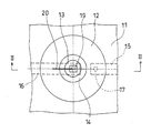
図1〜図2は、第1の実施の形態を示す。この第1の実施の形態は、一つのLEDチップを使用した場合である。
【0025】
この図において、符号11は、例えばガラスエポキシ樹脂(ガラス繊維をエポキシ樹脂で固めたもの)等の絶縁体製の配線基板を示し、この配線基板11の上面に、銅箔の表面にニッケルメッキ層を下地として金メッキ層を形成して成る金属膜による第1電極パターン12及び第2電極パターン13を形成する。
【0026】
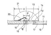
この場合において、前記第1電極パターン12は、直径Dの円形であり、この第1電極パターン12における中心部分に、電極なしの抜き孔14を設ける一方、前記第2電極パターン13を、小径dにして、この第2電極パターン13を、前記第1電極パターン12における抜き孔14内に、島状に独立して配設するようにする。
【0027】
また、前記配線基板11における下面に、前記第1電極パターン12に対する通電用配線パターン15と、前記第2電極パターン13に対する通電用配線パターン16とを形成して、これら各通電用配線パターン15,16と、前記両電極パターン12,13とを配線基板11を貫通するスルーホール17,18にて電気的に接続する。
【0028】
そして、前記第2電極パターン13における上面のうち前記第1電極パターン12における円の中心の部位に、LEDチップ19をダイボンディングにて搭載したのち、このLEDチップ19と、前記第1電極パターン12との間を、細い金属線20によるワイヤボンディングにて電気的に接続する。
【0029】
次いで、前記配線基板11の上面のうち前記第1電極パターン12の部分(好ましくは、第1電極パターン12における略中心部分)に、従来から良く知られているポッティング方法により、エポキシ樹脂等の透明合成樹脂を液体の状態で適宜量滴下する。
【0030】
この場合において、前記円形の第1電極パターン12は、LEDチップ19を搭載する第2電極パターン13の周囲の全体を完全に囲うとともに、当該第1電極パターン12の外周円の縁は、円の途中に分断箇所のない完全に閉じるように連続した円になっていることにより、これに滴下した液体の透明合成樹脂は、円形の第1電極パターン12の上面を伝って半径方法外向きに広がったのち、当該第1電極パターン12の外周円の縁に至り、その表面張力で第1電極パターン12の上面に、前記外周円の縁の総てからはみ出すことがない状態で略半球状に盛り上がることになる。
【0031】
そこで、前記のように盛り上げた液体の透明合成樹脂を、加熱等にて硬化することにより、略半球状のレンズ体21を、当該レンズ体21にて前記LEDチップ19及び金属線20をパッケージするようにして形成することができる。
【0032】
次に、図1〜図2は、第2の実施の形態を示す。この第2の実施の形態は、同じ色か、又は異なった色を発光する二つのLEDチップを使用した場合である。
【0033】
この図において、符号11aは、絶縁体製の配線基板を示し、この配線基板11aの上面には、前記第1の実施の形態と同様に金属膜による第1電極パターン12a及び二つの第2電極パターン13a,13a′を形成する。
【0034】
この場合において、前記第1電極パターン12aは、直径Dの円形であり、この第1電極パターン12aにおける中心部分に、電極なしの抜き孔14aを設ける一方、前記二つの第2電極パターン13a,13a′を、小径dにして、この両第2電極パターン13a,13a′を、前記第1電極パターン12aにおける抜き孔14a内に、平面視(図3)において、前記第1電極パターン12aにおける円の中心、又は、その近傍を中心とする半径rの円s、つまり、前記円形の第1電極パターン12aと略同心円sの円周方向に沿って等しい間隔にして、島状に独立して配設する。
【0035】
また、前記配線基板11aの下面に、前記第1電極パターン12aにスルーホール17aを介して電気的に接続する通電用配線パターン15a、前記両第2電極パターン13a,13a′のうち一方の第2電極パターン13aにスルーホール18aを介して電気的に接続する通電用配線パターン16a、及び、他方の第2電極パターン13a′にスルーホール18a′を介して電気的に接続する通電用配線パターン16a′を各々形成する。
【0036】
そして、前記両第2電極パターン13a,13a′における上面のうちその略中心の各々に、LEDチップ19a,19a′をダイボンディングにて搭載したのち、この両LEDチップ19a,19a′と、前記第1電極パターン12aとの間の各々を、細い金属線20a,20a′によるワイヤボンディングにて電気的に接続する。
【0037】
この場合において、前記両金属線20a,20a′は、平面視(図3)において、その各々におけるLEDチップ19a,19a′から互いに反対の方向に延びるように、つまり、半径方向外向きの放射状に延びるように配設する。
【0038】
次いで、前記第1の実施の形態の場合と同様に、前記配線基板11aの上面のうち前記第1電極パターン12aの部分(好ましくは、第1電極パターン12aにおける略中心部分)に、透明合成樹脂を液体の状態で適宜量滴下して、この液体の透明合成樹脂を、略半球状に盛り上げ、この状態で硬化することにより、略半球形のレンズ体21aを、当該レンズ体21aにて前記両LEDチップ19a,19a′及び金属線20a,20a′をパッケージするようにして形成することができる。
【0039】
この場合において、前記両LEDチップ19a,19a′に対する金属線20a,20a′は、互いに反対の方向に延びるように、つまり、半径方向外向きの放射状に延びていることにより、前記第1電極パターン12aに対して滴下した液体の透明合成樹脂における半径方向外向きへの流れは、前記両金属線20a,20a′の箇所において略同じようになるから、前記液体の透明合成樹脂は、平面視(図3)において、確実に真円に広がるのである。
【0040】
また、前記第1電極パターン12aのうちその抜き孔14aの内周縁の部分には、前記各第2電極パターン13a,13a′間への入り込み部12a′,12a″を備えている。この入り込み部12a′,12a″を備えていることにより、第1電極パターン12aにおける光の反射面を、各第2電極パターン13a,13a′の間の部分まで拡大することができる。
【0041】
次に、図5及び図6は、第3の実施の形態を示す。
【0042】
この第3の実施の形態は、赤色発光LEDチップ、緑色発光LEDチップ及び青色発光LEDチップの三つのLEDチップを使用した場合である。
【0043】
この図において、符号11bは、絶縁体製の配線基板を示し、この配線基板11bの上面には、前記第1及び第2の実施の形態と同様に金属膜による第1電極パターン12b及び三つの第2電極パターン13b,13b′,13b″を形成する。
【0044】
この場合において、前記第1電極パターン12bは、直径Dの円形であり、この第1電極パターン12bにおける中心部分に、電極なしの抜き孔14bを設ける一方、前記三つの第2電極パターン13b,13b′,13b″を、小径dにして、この各第2電極パターン13b,13b′,13b″を、前記第1電極パターン12bにおける抜き孔14b内に、平面視(図5)において、前記第1電極パターン12bにおける円の中心、又は、その近傍を中心とする半径rの円s、つまり、前記円形の第1電極パターン12bと略同心円sの円周方向に沿って120度の略等しい間隔にして、島状に独立して配設する。
【0045】
また、前記配線基板11bの下面に、前記第1電極パターン12bにスルーホール17bを介して電気的に接続する通電用配線パターン15b、前記各第2電極パターン13b,13b′,13b″のうち一つの第2電極パターン13bにスルーホール18bを介して電気的に接続する通電用配線パターン16b、別の一つの第2電極パターン13b′にスルーホール18b′を介して電気的に接続する通電用配線パターン16b′、及び、更に別の一つの第2電極パターン13b″にスルーホール18b″を介して電気的に接続する通電用配線パターン16b″を各々形成する。
【0046】
そして、前記各第2電極パターン13b,13b′,13b″のうち一つの一つの第2電極パターン13bには、赤色発光LEDチップ19bを、別の一つの第2電極パターン13b′には、緑色発光LEDチップ19b′を、そして、更に別の一つの第2電極パターン13b″には、青色発光LEDチップ19b″ダイボンディングにて搭載したのち、この各LEDチップ19b,19b′,19b″と、前記第1電極パターン12bとの間の各々を、細い金属線20b,20b′,20b″によるワイヤボンディングにて電気的に接続する。
【0047】
この場合において、前記各金属線20b,20b′,20b″は、平面視(図5)において、半径方向外向きの放射状に延びるように配設する。
【0048】
次いで、前記第1及び第2の実施の形態の場合と同様に、前記配線基板11bの上面のうち前記第1電極パターン12bの部分(好ましくは、第1電極パターン12bにおける略中心部分)に、透明合成樹脂を液体の状態で適宜量滴下して、この液体の透明合成樹脂を、略半球状に盛り上げ、この状態で硬化することにより、略半球形のレンズ体21bを、当該レンズ体21bにて前記各LEDチップ19b,19b′,19b″及び金属線20b,20b′,20b″をパッケージするようにして形成することができる。
【0049】
この場合において、前記各LEDチップ19b,19b′,19b″に対する金属線20b,20b′,20b″は、半径方向外向きの放射状に延びていることにより、前記第1電極パターン12bに対して滴下した液体の透明合成樹脂における半径方向外向きへの流れは、前記各金属線20b,20b′,20b″の箇所において略同じようになるから、前記液体の透明合成樹脂は、平面視(図5)において、確実に真円に広がるのである。
【0050】
また、この第3の実施の形態においても、前記第1電極パターン12bのうちその抜き孔14bの内周縁の部分には、前記各第2電極パターン13b,13b′,13b″間への入り込み部12b′を備えている。この入り込み部12b′を備えていることにより、第1電極パターン12bにおける光の反射面を、各第2電極パターン13b,13b′,13b″の間の部分まで拡大することができる。
【0051】
そして、図7,図8及び図9は、第4の実施形態を示す。
【0052】
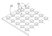
この第4の実施の形態は、前記第3の実施の形態による発光装置22の多数個を、一つの共通配線基板23に、縦及び横方向に並べて設けることにより、全体として、文字又は画像を光の三原色によるフルカラーにて表示するパネルに構成した場合である。
【0053】
この第4の実施の形態においては、前記共通配線基板23の表面のうち各発光装置22における円形の第1電極パターン12bを除く部分の全体に導体パターン24を、第1電極パターン12bとの間にリング状隙間25をあけて形成し、この導体パターン24に対して、前記各発光装置22における円形の第1電極パターン12bを、共通配線基板23の裏面側に形成した通電用配線パターン26及びスルーホール27,28,29を介して電気的に接続するという構成にしたものである。
【0054】
なお、前記導体パターン24の表面は、二点鎖線で示すように、絶縁膜30にて被覆されている。
【0055】
この構成によると、各発光装置22における第1電極パターン12bと、導体パターン24との間には、リング状隙間25をあけられ、前記第1電極パターン12bは、完全な円形になっているので、前記した効果を有し、しかも、前記各発光装置22における第1電極パターン12bに対する通電を、共通配線基板23の表面に形成した導体パターン24に行うことができることにより、各発光装置22に対する通電用配線パターンの構造を簡単化できる利点がある。
【図面の簡単な説明】
【図1】本発明における第1の実施の形態を示す平面図である。
【図2】図1のII−II視断面図である。
【図3】本発明における第2の実施の形態を示す平面図である。
【図4】図3のIV−IV視断面図である。
【図5】本発明における第3の実施の形態を示す平面図である。
【図6】図5のVI−VI視断面図である。
【図7】本発明における第4の実施の形態を示す斜視図である。
【図8】前記第4の実施の形態の要部を示す平面図である。
【図9】図8のIX−IX視断面図である。
【図10】先行技術の例を示す平面図である。
【図11】図10のXII −XII 視断面図である。
【図12】別の先行技術の例を示す視断面図である。
【符号の説明】
11,11a,11b 配線基板
12,12a,12b 第1電極パターン
13,13a,13b 第3電極パターン
14,14a,14b 抜き孔部
15,15a,15b 配線パターン
16,16a,16b 配線パターン
17,17a,17b スルーホール
18,18a,18b スルーホール
19,19a,19b LEDチップ
20,20a,20b 金属線
21,21a,21b レンズ体[0001]
BACKGROUND OF THE INVENTION
The present invention relates to a structure of a light emitting device in which an LED chip mounted on a wiring board or the like is packaged by a transparent synthetic resin lens body, and a manufacturing method thereof.
[0002]
[Prior art]
Generally speaking, this type of light emitting device has a pair of first electrode pattern and second electrode pattern formed on the upper surface of the wiring board, and an LED chip is mounted on the upper surface of the second electrode pattern. While the LED chip and the first electrode pattern are electrically connected by wire bonding using a thin metal wire, a lens body made of a transparent synthetic resin is formed on the LED chip portion of the upper surface of the wiring board. The LED chip and the metal wire are packaged with the lens body.
[0003]
JP-A-4-28269 as a prior art, as shown in FIG. 10 and FIG. 11, on the upper surface of the
[0004]
[Problems to be solved by the invention]
This prior art has a configuration in which the
[0005]
However, on the other hand, the circular
[0006]
That is, when a transparent synthetic resin for forming the
[0007]
As a result, the cured
[0008]
Therefore, in the prior art, in order to avoid this problem, a circular ring shape is formed on the upper surface of the circular
[0009]
However, forming the
[0010]
An object of the present invention is to provide a structure of a light emitting device that solves these problems and a manufacturing method thereof.
[0011]
[Means for Solving the Problems]
In order to achieve this technical problem, the structure of
“The first electrode pattern and the second electrode pattern formed of a metal film on the surface of the wiring board, the LED chip mounted on the second electrode pattern, and the LED chip and the first electrode pattern are electrically connected to each other. In a light emitting device comprising a metal wire connected to a lens body made of a transparent synthetic resin that packages the LED chip and the metal wire on the surface of the wiring board,
The first electrode pattern was made circular, and a hole without an electrode was provided at the center thereof, and the second electrode pattern was disposed in the hole. "
It is characterized by that.
[0012]
The structure of
“The first electrode pattern and the second electrode pattern formed of a metal film on the surface of the wiring board, the LED chip mounted on the second electrode pattern, and the LED chip and the first electrode pattern are electrically connected to each other. In a light emitting device comprising a metal wire connected to a lens body made of a transparent synthetic resin that packages the LED chip and the metal wire on the surface of the wiring board,
The first electrode pattern is circular, and a hole without an electrode is provided at the center thereof, while a plurality of the second electrode patterns are formed, and each of the second electrode patterns is formed in the first electrode pattern. In the punched hole portion, the circular first electrode pattern and the first electrode pattern mounted on each second electrode pattern are provided at substantially equal intervals along a circumferential direction substantially concentric with the circular first electrode pattern. The metal wires that electrically connect the two are arranged so as to extend radially outward in the radial direction. "
It is characterized by that.
[0013]
The structure of
“In the first or second aspect of the present invention, a current-carrying wiring pattern that is electrically connected to the first electrode pattern and the second electrode pattern through a through-hole in the wiring board is formed on the back surface of the wiring board. "
It is characterized by that.
[0014]
The structure of claim 4 of the present invention is:
“In the description of
It is characterized by that.
[0015]
Next, the manufacturing method according to
“A step of forming a first electrode pattern made of a metal film in a circular shape on a wiring board and providing a hole without an electrode at the center thereof, and forming a second electrode pattern made of a metal film in the hole. A step of mounting an LED chip on the second electrode pattern, a step of electrically connecting the LED chip and the first electrode pattern with a metal wire, and a liquid to the first electrode pattern The transparent synthetic resin includes a step of dripping the transparent synthetic resin so that the transparent synthetic resin covers the LED chip and the metal wire, and then curing to form a lens body. "
It is characterized by that.
[0016]
[Operation and effect of the invention]
As described above, when the first electrode pattern is made circular, a hole portion without an electrode is provided in the central portion, and the second electrode pattern is disposed in the hole portion. The circular first electrode pattern completely surrounds the entire periphery of the second electrode pattern on which the LED chip is mounted, and the edge of the outer peripheral circle of the first electrode pattern is completely free from any part of the circle. When forming a lens body made of a transparent synthetic resin by forming a continuous circle so as to close, when an appropriate amount of a liquid transparent synthetic resin is dropped onto the first electrode pattern, the liquid transparent synthetic resin is Then, after spreading outward in the radial direction along the upper surface of the circular first electrode pattern, it reaches the edge of the outer circumference circle of the first electrode pattern, and the outer circumference circles on the upper surface of the first electrode pattern by its surface tension. Since it swells in a substantially hemispherical shape without protruding from all edges, the liquid transparent synthetic resin that swells protrudes outward from a part of the edge of the outer circumference circle as in the case of the prior art. Thus, it is possible to reliably avoid the lens body from becoming an irregular shape.
[0017]
The circular first electrode pattern and the second electrode pattern in the hole in the first electrode pattern are both metal films, so that the light emitted from the LED chip is reflected in the direction away from the wiring board. It becomes a reflection of doing.
[0018]
Therefore, according to the present invention, the light from the LED chip can be reliably reflected in the direction of the lens body by each electrode pattern, while the lens body can be formed into a predetermined shape and the lens shape can vary. It is possible to reduce the sticking, and it is not necessary to use a dam ring that surrounds the lens body as in the prior art, so that the brightness of light can be increased.
[0019]
According to
[0020]
According to the third aspect, energization of the first electrode pattern and the second electrode pattern can be performed by the energization wiring pattern on the back surface side of the wiring substrate, so that the energization wiring pattern can be easily formed.
[0021]
According to the fourth aspect, since the light reflection surface of the first electrode pattern can be expanded to the portion between the second electrode patterns, the luminance of the light can be further increased.
[0022]
Furthermore, according to the manufacturing method of
[0023]
DETAILED DESCRIPTION OF THE INVENTION
Hereinafter, embodiments of the present invention will be described with reference to the drawings.
[0024]
1 to 2 show a first embodiment. In the first embodiment, one LED chip is used.
[0025]
In this figure,
[0026]
In this case, the
[0027]
Further, a current-carrying
[0028]
And after mounting
[0029]
Next, a transparent portion such as an epoxy resin is applied to the portion of the first electrode pattern 12 (preferably, the substantially central portion of the first electrode pattern 12) of the upper surface of the
[0030]
In this case, the circular
[0031]
Therefore, the liquid transparent synthetic resin raised as described above is cured by heating or the like, so that the substantially
[0032]
Next, FIGS. 1 to 2 show a second embodiment. In the second embodiment, two LED chips that emit the same color or different colors are used.
[0033]
In this figure,
[0034]
In this case, the
[0035]
In addition, a
[0036]
Then, after
[0037]
In this case, both the
[0038]
Next, as in the case of the first embodiment, a transparent synthetic resin is formed on the portion of the
[0039]
In this case, the
[0040]
Further, in the
[0041]
Next, FIGS. 5 and 6 show a third embodiment.
[0042]
The third embodiment is a case where three LED chips, a red light emitting LED chip, a green light emitting LED chip, and a blue light emitting LED chip are used.
[0043]
In this figure, reference numeral 11b denotes an insulating wiring board. On the upper surface of the wiring board 11b, as in the first and second embodiments, a
[0044]
In this case, the
[0045]
Further, one of the energizing
[0046]
Of the
[0047]
In this case, the
[0048]
Next, as in the case of the first and second embodiments, the portion of the
[0049]
In this case, the
[0050]
Also in the third embodiment, a portion of the
[0051]
FIG. 7, FIG. 8, and FIG. 9 show a fourth embodiment.
[0052]
In the fourth embodiment, a large number of light emitting
[0053]
In the fourth embodiment, the
[0054]
The surface of the
[0055]
According to this configuration, the ring-shaped
[Brief description of the drawings]
FIG. 1 is a plan view showing a first embodiment of the present invention.
2 is a cross-sectional view taken along the line II-II of FIG.
FIG. 3 is a plan view showing a second embodiment of the present invention.
4 is a cross-sectional view taken along the line IV-IV in FIG. 3;
FIG. 5 is a plan view showing a third embodiment of the present invention.
6 is a cross-sectional view taken along the line VI-VI in FIG. 5;
FIG. 7 is a perspective view showing a fourth embodiment of the present invention.
FIG. 8 is a plan view showing a main part of the fourth embodiment.
9 is a cross-sectional view taken along the line IX-IX of FIG.
FIG. 10 is a plan view showing an example of the prior art.
11 is a cross-sectional view taken along line XII-XII in FIG.
FIG. 12 is a cross-sectional view showing another prior art example.
[Explanation of symbols]
11, 11a,
Claims (5)
前記第1電極パターンを、円形にして、その中心部分に、電極なしの抜き孔部を設けて、この抜き孔部内に、前記第2電極パターンを配設したことを特徴とするLEDチップを使用した発光装置の構造。A first electrode pattern and a second electrode pattern formed of a metal film on the surface of the wiring board, an LED chip mounted on the second electrode pattern, and the LED chip and the first electrode pattern are electrically connected to each other. In a light emitting device comprising a metal wire to be connected and a lens body made of a transparent synthetic resin for packaging the LED chip and the metal wire on the surface of the wiring board,
An LED chip is used, wherein the first electrode pattern is circular, and a hole portion without an electrode is provided at a central portion thereof, and the second electrode pattern is disposed in the hole portion. Structure of the light emitting device.
前記第1電極パターンを、円形にして、その中心部分に、電極なしの抜き孔部を設ける一方、前記第2電極パターンを複数個にし、この各第2電極パターンを、前記第1電極パターンにおける抜き孔部内に、前記円形の第1電極パターンとと略同心円の円周方向に沿って略等しい間隔にして配設し、更に、前記各第2電極パターンに搭載したLEDチップと前記第1電極パターンとを電気的に接続する金属線を、半径方向外向きの放射状に延びるように配設したことを特徴とするLEDチップを使用した発光装置の構造。A first electrode pattern and a second electrode pattern formed of a metal film on the surface of the wiring board, an LED chip mounted on the second electrode pattern, and the LED chip and the first electrode pattern are electrically connected to each other. In a light emitting device comprising a metal wire to be connected and a lens body made of a transparent synthetic resin for packaging the LED chip and the metal wire on the surface of the wiring board,
The first electrode pattern is circular, and a hole without an electrode is provided at the center thereof, while a plurality of the second electrode patterns are formed, and each of the second electrode patterns is formed in the first electrode pattern. The LED chip and the first electrode mounted in each of the second electrode patterns are disposed in the punched holes at substantially equal intervals along a circumferential direction substantially concentric with the circular first electrode pattern. A structure of a light-emitting device using an LED chip, wherein metal wires that electrically connect a pattern are arranged to extend radially outward in a radial direction.
Priority Applications (5)
| Application Number | Priority Date | Filing Date | Title |
|---|---|---|---|
| JP2002059122A JP3801931B2 (en) | 2002-03-05 | 2002-03-05 | Structure and manufacturing method of light emitting device using LED chip |
| US10/505,845 US7126159B2 (en) | 2002-03-05 | 2003-03-03 | Plural leds mounted within a central cutout of a surrounding circular reflective electrode |
| KR1020037016751A KR100862985B1 (en) | 2002-03-05 | 2003-03-03 | Light emitting device utilizing led chip and method of making the same |
| EP03743566A EP1482567A4 (en) | 2002-03-05 | 2003-03-03 | Light-emitting device comprising led chip and method for manufacturing this device |
| PCT/JP2003/002448 WO2003075367A1 (en) | 2002-03-05 | 2003-03-03 | Light-emitting device comprising led chip and method for manufacturing this device |
Applications Claiming Priority (1)
| Application Number | Priority Date | Filing Date | Title |
|---|---|---|---|
| JP2002059122A JP3801931B2 (en) | 2002-03-05 | 2002-03-05 | Structure and manufacturing method of light emitting device using LED chip |
Publications (2)
| Publication Number | Publication Date |
|---|---|
| JP2003258313A JP2003258313A (en) | 2003-09-12 |
| JP3801931B2 true JP3801931B2 (en) | 2006-07-26 |
Family
ID=27784730
Family Applications (1)
| Application Number | Title | Priority Date | Filing Date |
|---|---|---|---|
| JP2002059122A Expired - Fee Related JP3801931B2 (en) | 2002-03-05 | 2002-03-05 | Structure and manufacturing method of light emitting device using LED chip |
Country Status (5)
| Country | Link |
|---|---|
| US (1) | US7126159B2 (en) |
| EP (1) | EP1482567A4 (en) |
| JP (1) | JP3801931B2 (en) |
| KR (1) | KR100862985B1 (en) |
| WO (1) | WO2003075367A1 (en) |
Cited By (1)
| Publication number | Priority date | Publication date | Assignee | Title |
|---|---|---|---|---|
| KR101488451B1 (en) * | 2008-03-31 | 2015-02-02 | 서울반도체 주식회사 | Multi chip led package |
Families Citing this family (83)
| Publication number | Priority date | Publication date | Assignee | Title |
|---|---|---|---|---|
| JPS6359360A (en) * | 1986-08-29 | 1988-03-15 | Koito Mfg Co Ltd | Super-wide-angle nozzle for head lamp cleaner |
| US7675075B2 (en) * | 2003-08-28 | 2010-03-09 | Panasonic Corporation | Semiconductor light emitting device, light emitting module, lighting apparatus, display element and manufacturing method of semiconductor light emitting device |
| US7915085B2 (en) | 2003-09-18 | 2011-03-29 | Cree, Inc. | Molded chip fabrication method |
| US7781789B2 (en) * | 2006-11-15 | 2010-08-24 | The Regents Of The University Of California | Transparent mirrorless light emitting diode |
| JP2005353802A (en) * | 2004-06-10 | 2005-12-22 | Citizen Electronics Co Ltd | Light emitting diode |
| US7534633B2 (en) | 2004-07-02 | 2009-05-19 | Cree, Inc. | LED with substrate modifications for enhanced light extraction and method of making same |
| JP2006114737A (en) * | 2004-10-15 | 2006-04-27 | Akita Denshi Systems:Kk | Optical semiconductor equipment and manufacturing method thereof |
| US9793247B2 (en) * | 2005-01-10 | 2017-10-17 | Cree, Inc. | Solid state lighting component |
| US9070850B2 (en) | 2007-10-31 | 2015-06-30 | Cree, Inc. | Light emitting diode package and method for fabricating same |
| JP4727314B2 (en) * | 2005-06-21 | 2011-07-20 | ローム株式会社 | Display panel device using light emitting diode |
| US8835952B2 (en) | 2005-08-04 | 2014-09-16 | Cree, Inc. | Submounts for semiconductor light emitting devices and methods of forming packaged light emitting devices including dispensed encapsulants |
| US7365371B2 (en) | 2005-08-04 | 2008-04-29 | Cree, Inc. | Packages for semiconductor light emitting devices utilizing dispensed encapsulants |
| JP2007053318A (en) * | 2005-08-19 | 2007-03-01 | Matsushita Electric Ind Co Ltd | Solid-state imaging device and method of manufacturing same |
| DE102005048498B4 (en) * | 2005-10-07 | 2007-06-21 | Schefenacker Vision Systems Germany Gmbh | Multicolored vehicle exterior light |
| JP4954664B2 (en) * | 2005-10-20 | 2012-06-20 | 昭和電工株式会社 | Light emitting element mounting substrate, light emitting element mounting package, and surface light source device |
| US20090225541A1 (en) * | 2005-10-20 | 2009-09-10 | Showa Denko K.K. | Luminous device mounting substrate, luminous device mounting package, and planar light source device |
| US20070096139A1 (en) * | 2005-11-02 | 2007-05-03 | 3M Innovative Properties Company | Light emitting diode encapsulation shape control |
| JP4724618B2 (en) * | 2005-11-11 | 2011-07-13 | 株式会社 日立ディスプレイズ | LIGHTING DEVICE AND LIQUID CRYSTAL DISPLAY DEVICE USING THE SAME |
| US20090001388A1 (en) * | 2006-01-19 | 2009-01-01 | Rohm Co., Ltd. | Semiconductor Display Device and Method for Manufacturing The Same |
| KR100828891B1 (en) | 2006-02-23 | 2008-05-09 | 엘지이노텍 주식회사 | LED Package |
| KR100782771B1 (en) * | 2006-03-14 | 2007-12-05 | 삼성전기주식회사 | Manufacturing process for LED package |
| JP4823729B2 (en) * | 2006-03-20 | 2011-11-24 | ローム株式会社 | Optical communication module |
| US8969908B2 (en) * | 2006-04-04 | 2015-03-03 | Cree, Inc. | Uniform emission LED package |
| KR100755615B1 (en) * | 2006-04-14 | 2007-09-06 | 삼성전기주식회사 | Backlight for liquid crystal display comprising light emitting diode |
| US9335006B2 (en) | 2006-04-18 | 2016-05-10 | Cree, Inc. | Saturated yellow phosphor converted LED and blue converted red LED |
| US7547115B2 (en) * | 2006-05-23 | 2009-06-16 | Au Optronics Corporation | Package structure for light emitting diode and applications of the same |
| KR100804021B1 (en) * | 2006-07-11 | 2008-02-18 | 우리이티아이 주식회사 | Differential thickness encap type led package and methode the same |
| US7545461B2 (en) * | 2006-07-25 | 2009-06-09 | Kyocera Corporation | Liquid crystal display device |
| US7804147B2 (en) * | 2006-07-31 | 2010-09-28 | Cree, Inc. | Light emitting diode package element with internal meniscus for bubble free lens placement |
| US7808013B2 (en) * | 2006-10-31 | 2010-10-05 | Cree, Inc. | Integrated heat spreaders for light emitting devices (LEDs) and related assemblies |
| US10295147B2 (en) | 2006-11-09 | 2019-05-21 | Cree, Inc. | LED array and method for fabricating same |
| US7897980B2 (en) * | 2006-11-09 | 2011-03-01 | Cree, Inc. | Expandable LED array interconnect |
| US7769066B2 (en) | 2006-11-15 | 2010-08-03 | Cree, Inc. | Laser diode and method for fabricating same |
| WO2008060586A2 (en) * | 2006-11-15 | 2008-05-22 | The Regents Of The University Of California | Textured phosphor conversion layer light emitting diode |
| JP2010512662A (en) | 2006-12-11 | 2010-04-22 | ザ リージェンツ オブ ザ ユニバーシティ オブ カリフォルニア | Transparent light emitting diode |
| US7834367B2 (en) | 2007-01-19 | 2010-11-16 | Cree, Inc. | Low voltage diode with reduced parasitic resistance and method for fabricating |
| US8232564B2 (en) | 2007-01-22 | 2012-07-31 | Cree, Inc. | Wafer level phosphor coating technique for warm light emitting diodes |
| US9024349B2 (en) * | 2007-01-22 | 2015-05-05 | Cree, Inc. | Wafer level phosphor coating method and devices fabricated utilizing method |
| US9159888B2 (en) | 2007-01-22 | 2015-10-13 | Cree, Inc. | Wafer level phosphor coating method and devices fabricated utilizing method |
| JP4869165B2 (en) * | 2007-06-28 | 2012-02-08 | 昭和電工株式会社 | Method for manufacturing light emitting device |
| US9401461B2 (en) * | 2007-07-11 | 2016-07-26 | Cree, Inc. | LED chip design for white conversion |
| US10505083B2 (en) * | 2007-07-11 | 2019-12-10 | Cree, Inc. | Coating method utilizing phosphor containment structure and devices fabricated using same |
| JP5290543B2 (en) * | 2007-07-20 | 2013-09-18 | スタンレー電気株式会社 | Light emitting device |
| US8519437B2 (en) | 2007-09-14 | 2013-08-27 | Cree, Inc. | Polarization doping in nitride based diodes |
| US9012937B2 (en) | 2007-10-10 | 2015-04-21 | Cree, Inc. | Multiple conversion material light emitting diode package and method of fabricating same |
| KR20090058878A (en) * | 2007-12-05 | 2009-06-10 | 삼성전자주식회사 | Light emiting device, method of manufacturing the same and liquid crystal display having the same |
| US8167674B2 (en) | 2007-12-14 | 2012-05-01 | Cree, Inc. | Phosphor distribution in LED lamps using centrifugal force |
| US9041285B2 (en) | 2007-12-14 | 2015-05-26 | Cree, Inc. | Phosphor distribution in LED lamps using centrifugal force |
| US8878219B2 (en) * | 2008-01-11 | 2014-11-04 | Cree, Inc. | Flip-chip phosphor coating method and devices fabricated utilizing method |
| US8637883B2 (en) | 2008-03-19 | 2014-01-28 | Cree, Inc. | Low index spacer layer in LED devices |
| US8877524B2 (en) * | 2008-03-31 | 2014-11-04 | Cree, Inc. | Emission tuning methods and devices fabricated utilizing methods |
| US9425172B2 (en) | 2008-10-24 | 2016-08-23 | Cree, Inc. | Light emitter array |
| KR101077264B1 (en) * | 2009-02-17 | 2011-10-27 | (주)포인트엔지니어링 | Substrate for optical device, optical device package having the same and menufacturing method thereof |
| DE102009031008A1 (en) * | 2009-06-29 | 2010-12-30 | Osram Opto Semiconductors Gmbh | Optoelectronic component |
| JP2011077084A (en) * | 2009-09-29 | 2011-04-14 | Rohm Co Ltd | Led lighting system and liquid crystal display device |
| US8511851B2 (en) | 2009-12-21 | 2013-08-20 | Cree, Inc. | High CRI adjustable color temperature lighting devices |
| JP4951090B2 (en) * | 2010-01-29 | 2012-06-13 | 株式会社東芝 | LED package |
| JP2012004596A (en) * | 2010-01-29 | 2012-01-05 | Toshiba Corp | Led package and method of manufacturing the same |
| US10546846B2 (en) | 2010-07-23 | 2020-01-28 | Cree, Inc. | Light transmission control for masking appearance of solid state light sources |
| JP5297472B2 (en) * | 2011-01-18 | 2013-09-25 | ローム株式会社 | Display panel device using light emitting diode |
| US9786811B2 (en) | 2011-02-04 | 2017-10-10 | Cree, Inc. | Tilted emission LED array |
| JP5748496B2 (en) | 2011-02-10 | 2015-07-15 | ローム株式会社 | LED module |
| US8888331B2 (en) * | 2011-05-09 | 2014-11-18 | Microsoft Corporation | Low inductance light source module |
| JP2013004815A (en) * | 2011-06-17 | 2013-01-07 | Sony Corp | Light source circuit unit, lighting device, and display device |
| USD700584S1 (en) | 2011-07-06 | 2014-03-04 | Cree, Inc. | LED component |
| US10842016B2 (en) | 2011-07-06 | 2020-11-17 | Cree, Inc. | Compact optically efficient solid state light source with integrated thermal management |
| US8558252B2 (en) | 2011-08-26 | 2013-10-15 | Cree, Inc. | White LEDs with emission wavelength correction |
| JP5737083B2 (en) * | 2011-09-02 | 2015-06-17 | ウシオ電機株式会社 | LED light source device |
| WO2013136758A1 (en) * | 2012-03-15 | 2013-09-19 | パナソニック株式会社 | Substrate for led, led module, and led bulb |
| JP6021457B2 (en) * | 2012-06-18 | 2016-11-09 | 三菱電機株式会社 | Light emitting device |
| WO2014196833A1 (en) * | 2013-06-07 | 2014-12-11 | 서울반도체 주식회사 | Light-emitting device |
| JP6165537B2 (en) * | 2013-07-22 | 2017-07-19 | ローム株式会社 | LED lighting device |
| US9532464B2 (en) | 2013-07-22 | 2016-12-27 | Rohm Co., Ltd. | LED lighting apparatus |
| US10529897B2 (en) * | 2015-03-06 | 2020-01-07 | Koninklijke Philips N.V. | LED-based lighting device with asymmetrically distributed LED chips |
| JP6842234B2 (en) | 2015-10-13 | 2021-03-17 | ローム株式会社 | Manufacturing method of optical semiconductor device and optical semiconductor device |
| KR101987196B1 (en) | 2016-06-14 | 2019-06-11 | 삼성디스플레이 주식회사 | Pixel structure, display apparatus including the pixel structure and method of manufacturing the same |
| CN106486498B (en) * | 2016-10-14 | 2019-09-10 | 武汉华星光电技术有限公司 | A kind of display panel |
| JP2018206708A (en) * | 2017-06-08 | 2018-12-27 | シチズン電子株式会社 | Light emitting device |
| JP2019135512A (en) * | 2018-02-05 | 2019-08-15 | シャープ株式会社 | Stereoscopic display device, and aerial stereoscopic display device |
| JP7299768B2 (en) * | 2019-06-21 | 2023-06-28 | スタンレー電気株式会社 | Semiconductor device, substrate for mounting semiconductor element, and manufacturing method thereof |
| JP7222827B2 (en) | 2019-06-21 | 2023-02-15 | スタンレー電気株式会社 | Semiconductor device and manufacturing method thereof |
| US11592166B2 (en) | 2020-05-12 | 2023-02-28 | Feit Electric Company, Inc. | Light emitting device having improved illumination and manufacturing flexibility |
| US11876042B2 (en) | 2020-08-03 | 2024-01-16 | Feit Electric Company, Inc. | Omnidirectional flexible light emitting device |
Family Cites Families (24)
| Publication number | Priority date | Publication date | Assignee | Title |
|---|---|---|---|---|
| US3999280A (en) * | 1973-06-25 | 1976-12-28 | Amp Incorporated | Narrow lead contact for automatic face down bonding of electronic chips |
| JPS5511356A (en) * | 1978-07-11 | 1980-01-26 | Toshiba Corp | Light-emitting semiconductor display system |
| JPS611067A (en) * | 1984-06-13 | 1986-01-07 | Stanley Electric Co Ltd | Molding method of led chip mounted on printed board |
| FR2574616B1 (en) * | 1984-12-07 | 1987-01-23 | Radiotechnique Compelec | MATRIX OF ELECTRO-LUMINESCENT ELEMENT AND MANUFACTURING METHOD THEREOF |
| JPH0428269A (en) * | 1990-05-23 | 1992-01-30 | Fujikura Ltd | Mounting structure of led bare chip |
| US5557115A (en) * | 1994-08-11 | 1996-09-17 | Rohm Co. Ltd. | Light emitting semiconductor device with sub-mount |
| JPH10242523A (en) * | 1997-02-28 | 1998-09-11 | Kouha:Kk | Light emitting diode display device and picture display device utilizing the same |
| JPH10319871A (en) * | 1997-05-19 | 1998-12-04 | Kouha:Kk | Led display device |
| JP4056598B2 (en) * | 1997-10-09 | 2008-03-05 | シチズン電子株式会社 | Infrared data communication module |
| US6335548B1 (en) * | 1999-03-15 | 2002-01-01 | Gentex Corporation | Semiconductor radiation emitter package |
| JP2000353826A (en) * | 1999-06-09 | 2000-12-19 | Sanyo Electric Co Ltd | Hybrid integrated circuit device and light irradiating device |
| JP4190095B2 (en) * | 1999-07-29 | 2008-12-03 | 三洋電機株式会社 | Hybrid integrated circuit device |
| JP2001044579A (en) * | 1999-07-29 | 2001-02-16 | Sanyo Electric Co Ltd | Hybrid integrated circuit device |
| JP4342046B2 (en) * | 1999-07-29 | 2009-10-14 | 三洋電機株式会社 | Metal substrate type light emitting device |
| EP1059668A3 (en) | 1999-06-09 | 2007-07-18 | Sanyo Electric Co., Ltd. | Hybrid integrated circuit device |
| JP4412787B2 (en) * | 1999-06-09 | 2010-02-10 | 三洋電機株式会社 | Irradiation device and irradiation module using metal substrate |
| JP2001068742A (en) * | 1999-08-25 | 2001-03-16 | Sanyo Electric Co Ltd | Hybrid integrated circuit device |
| GB0000511D0 (en) * | 2000-01-12 | 2000-03-01 | Oxley Dev Co Ltd | Led package |
| JP2001351404A (en) * | 2000-04-06 | 2001-12-21 | Kansai Tlo Kk | Surface emitting device using light-emitting diode |
| DE10033502A1 (en) * | 2000-07-10 | 2002-01-31 | Osram Opto Semiconductors Gmbh | Optoelectronic module, process for its production and its use |
| US6611000B2 (en) * | 2001-03-14 | 2003-08-26 | Matsushita Electric Industrial Co., Ltd. | Lighting device |
| JP2002319711A (en) * | 2001-04-20 | 2002-10-31 | Citizen Electronics Co Ltd | Surface mounting type light-emitting diode and method for manufacturing the same |
| US6531328B1 (en) * | 2001-10-11 | 2003-03-11 | Solidlite Corporation | Packaging of light-emitting diode |
| TW578280B (en) * | 2002-11-21 | 2004-03-01 | United Epitaxy Co Ltd | Light emitting diode and package scheme and method thereof |
-
2002
- 2002-03-05 JP JP2002059122A patent/JP3801931B2/en not_active Expired - Fee Related
-
2003
- 2003-03-03 EP EP03743566A patent/EP1482567A4/en not_active Withdrawn
- 2003-03-03 KR KR1020037016751A patent/KR100862985B1/en active IP Right Grant
- 2003-03-03 US US10/505,845 patent/US7126159B2/en not_active Expired - Lifetime
- 2003-03-03 WO PCT/JP2003/002448 patent/WO2003075367A1/en active Application Filing
Cited By (1)
| Publication number | Priority date | Publication date | Assignee | Title |
|---|---|---|---|---|
| KR101488451B1 (en) * | 2008-03-31 | 2015-02-02 | 서울반도체 주식회사 | Multi chip led package |
Also Published As
| Publication number | Publication date |
|---|---|
| KR20040093383A (en) | 2004-11-05 |
| EP1482567A1 (en) | 2004-12-01 |
| EP1482567A4 (en) | 2010-03-31 |
| KR100862985B1 (en) | 2008-10-13 |
| JP2003258313A (en) | 2003-09-12 |
| US7126159B2 (en) | 2006-10-24 |
| WO2003075367A1 (en) | 2003-09-12 |
| EP1482567A9 (en) | 2005-11-02 |
| US20050122031A1 (en) | 2005-06-09 |
Similar Documents
| Publication | Publication Date | Title |
|---|---|---|
| JP3801931B2 (en) | Structure and manufacturing method of light emitting device using LED chip | |
| JP3956965B2 (en) | Chip component type light emitting device and wiring board therefor | |
| JP6541963B2 (en) | Light emitting device and method of manufacturing the same | |
| JP2008053718A (en) | Light emitting device, manufacturing method thereof, and light unit | |
| JP2009033088A (en) | Semiconductor light-emitting device, method for producing the same, and led illuminating apparatus using the same | |
| JP2005327786A (en) | Method of manufacturing light emitting diode element | |
| JP4593201B2 (en) | Chip component type light emitting device and wiring board therefor | |
| JP2004087935A (en) | Semiconductor light-emitting device | |
| JP2012099572A (en) | Light emitting device | |
| JPH096259A (en) | Led display | |
| EP1482540A1 (en) | Method for forming thin film | |
| JP2009283988A (en) | Light emitting diode | |
| KR20090016217A (en) | Light emitting diode package and method thereof | |
| JPH02132489A (en) | Resin sealing structure of light emitting element to printed board | |
| JP3989518B2 (en) | LED display substrate and LED display | |
| JP3459487B2 (en) | LED display board and LED display | |
| JP3889725B2 (en) | LED indicator | |
| KR20110110608A (en) | Light emitting device packag and method for fabricating thereof | |
| JPS5926609Y2 (en) | Optical semiconductor display device | |
| CN103928597A (en) | Light-emitting diode element substrate provided with thick film reflecting layer, element and manufacturing method | |
| JP5841325B2 (en) | Bare chip mounting surface light emitter | |
| JPH04120984U (en) | dot matrix light emitting display | |
| CN103928598A (en) | Light-emitting diode element substrate provided with thick film surrounding wall, element and manufacturing method | |
| KR101324697B1 (en) | Board for light emitting device package, method for fabricating light emitting device package and light emitting device package by the same method | |
| JP4453004B2 (en) | Wiring board for mounting light-emitting elements |
Legal Events
| Date | Code | Title | Description |
|---|---|---|---|
| TRDD | Decision of grant or rejection written | ||
| A01 | Written decision to grant a patent or to grant a registration (utility model) |
Free format text: JAPANESE INTERMEDIATE CODE: A01 Effective date: 20060411 |
|
| A61 | First payment of annual fees (during grant procedure) |
Free format text: JAPANESE INTERMEDIATE CODE: A61 Effective date: 20060426 |
|
| R150 | Certificate of patent or registration of utility model |
Free format text: JAPANESE INTERMEDIATE CODE: R150 Ref document number: 3801931 Country of ref document: JP Free format text: JAPANESE INTERMEDIATE CODE: R150 |
|
| FPAY | Renewal fee payment (event date is renewal date of database) |
Free format text: PAYMENT UNTIL: 20090512 Year of fee payment: 3 |
|
| FPAY | Renewal fee payment (event date is renewal date of database) |
Free format text: PAYMENT UNTIL: 20120512 Year of fee payment: 6 |
|
| FPAY | Renewal fee payment (event date is renewal date of database) |
Free format text: PAYMENT UNTIL: 20130512 Year of fee payment: 7 |
|
| FPAY | Renewal fee payment (event date is renewal date of database) |
Free format text: PAYMENT UNTIL: 20140512 Year of fee payment: 8 |
|
| R250 | Receipt of annual fees |
Free format text: JAPANESE INTERMEDIATE CODE: R250 |
|
| LAPS | Cancellation because of no payment of annual fees |