JP3732362B2 - Game machine - Google Patents
Game machine Download PDFInfo
- Publication number
- JP3732362B2 JP3732362B2 JP22894399A JP22894399A JP3732362B2 JP 3732362 B2 JP3732362 B2 JP 3732362B2 JP 22894399 A JP22894399 A JP 22894399A JP 22894399 A JP22894399 A JP 22894399A JP 3732362 B2 JP3732362 B2 JP 3732362B2
- Authority
- JP
- Japan
- Prior art keywords
- prize ball
- game
- display
- control microcomputer
- payout
- Prior art date
- Legal status (The legal status is an assumption and is not a legal conclusion. Google has not performed a legal analysis and makes no representation as to the accuracy of the status listed.)
- Expired - Fee Related
Links
Images


Landscapes
- Pinball Game Machines (AREA)
Description
【0001】
【発明の属する技術分野】
本発明は、パチンコ遊技機等の遊技機に関し、特に、遊技者の操作によって遊技領域に遊技媒体が発射され、遊技媒体が遊技領域に設けられた入賞領域に入賞すると所定の価値が遊技者に付与されるとともに、特定入賞部への遊技媒体の進入により特別遊技を行い、特別遊技の結果が所定の態様になったことにもとづいて遊技者に所定の遊技価値が付与可能となる遊技機に関する。
【0002】
【従来の技術】
遊技機として、遊技球などの遊技媒体を発射装置によって遊技領域に発射し、遊技領域に設けられている入賞口などの入賞領域に遊技媒体が入賞すると、所定個の賞球が遊技者に払い出されるものがある。さらに、表示状態が変化可能な可変表示部が設けられ、可変表示部の表示結果があらかじめ定められた特定の表示態様となった場合に所定の遊技価値を遊技者に与えるように構成されたものがある。
【0003】
特別図柄を表示する可変表示部の表示結果があらかじめ定められた特定の表示態様の組合せとなることを、通常、「大当り」という。なお、遊技価値とは、遊技機の遊技領域に設けられた可変入賞球装置の状態が打球が入賞しやすい遊技者にとって有利な状態になることや、遊技者にとって有利な状態となるための権利を発生させたりすることである。
【0004】
大当りが発生すると、例えば、大入賞口が所定回数開放して打球が入賞しやすい大当り遊技状態に移行する。そして、各開放期間において、所定個(例えば10個)の大入賞口への入賞があると大入賞口は閉成する。そして、大入賞口の開放回数は、所定回数(例えば16ラウンド)に固定されている。なお、各開放について開放時間(例えば29.5秒)が決められ、入賞数が所定個に達しなくても開放時間が経過すると大入賞口は閉成する。また、大入賞口が閉成した時点で所定の条件(例えば、大入賞口内に設けられているVゾーンへの入賞)が成立していない場合には、大当り遊技状態は終了する。
【0005】
また、「大当り」の組合せ以外の表示態様の組合せのうち、複数の可変表示部の表示結果のうちの一部が未だに導出表示されていない段階において、既に表示結果が導出表示されている可変表示部の表示態様が特定の表示態様の組合せとなる表示条件を満たしている状態を「リーチ」という。そして、可変表示部に可変表示される識別情報の表示結果が「リーチ」となる条件を満たさない場合には「はずれ」となり、可変表示状態は終了する。遊技者は、大当りをいかにして発生させるかを楽しみつつ遊技を行う。
【0006】
遊技機における遊技進行はマイクロコンピュータ等による遊技制御手段によって制御される。可変表示装置に表示される識別情報、キャラクタ画像および背景画像は、遊技制御手段からの表示制御コマンドデータに従って動作する表示制御手段によって制御される。可変表示装置に表示される識別情報、キャラクタ画像および背景画像は、一般に、表示制御用のマイクロコンピュータとマイクロコンピュータの指示に応じて画像データを生成して可変表示装置側に転送するビデオディスプレイプロセッサ(VDP)とによって制御されるが、表示制御用のマイクロコンピュータのプログラム容量は大きい。
【0007】
従って、プログラム容量に制限のある遊技制御手段のマイクロコンピュータで可変表示装置に表示される識別情報等を制御することはできず、遊技制御手段のマイクロコンピュータとは別の表示制御用のマイクロコンピュータ(表示制御手段)が用いられる。よって、遊技の進行を制御する遊技制御手段は、表示制御手段に対して表示制御のためのコマンドを送信する必要がある。
【0008】
また、遊技者は、一般に、遊技媒体を遊技機を介して借り出す。その場合、遊技媒体貸出機構が遊技機に設けられる。遊技媒体貸出機構は、賞球払出を行う払出機構と共通化されることも多い。遊技媒体貸出機構と賞球払出機構とが共通化されている場合でも別個に設けられている場合でも、ともに遊技媒体を払い出す動作を行うのであるから、それらは、一般に、一つの賞球制御基板に搭載された賞球制御手段によって制御される。
【0009】
遊技の進行は主基板に搭載された遊技制御手段によって制御されるので、入賞にもとづく賞球個数は、遊技制御手段によって決定され、賞球制御基板に送信される。一方、遊技媒体の貸し出しは、遊技の進行とは無関係であるから、一般に、遊技制御手段を介さず賞球制御手段によって制御される。
【0010】
【発明が解決しようとする課題】
以上のように、遊技機には、遊技制御手段の他に種々の制御手段が搭載されている。一般に、各制御手段はマイクロコンピュータで構成される。すなわち、ROM等にプログラムが格納され、制御上一時的に発生するデータや制御進行に伴って変化するデータがRAMに格納される。すると、遊技機に停電等による電源断状態が発生すると、RAM内のデータは失われてしまう。よって、停電等からの復旧時には、最初の状態(例えば、遊技店においてその日最初に遊技機に電源投入されたときの状態)に戻さざるを得ないので、遊技者に不利益がもたらされる可能性がある。例えば、大当たり遊技中において電源断が発生し遊技機が最初の状態に戻ってしまうのでは、遊技者は大当たりの発生にもとづく利益を享受することができなくなってしまう。
【0011】
そのような事態を回避するには、停電等の不測の電源断が生じたときに、必要なデータを電源バックアップRAMに保存し、電源が復旧したときに保存されていたデータを復元して遊技を再開させればよい。しかし、電源断時に必要なデータを保存する際に保存の仕方および復元の仕方が不適切であると、復元されたデータが電源断時のデータと一致しない可能性がある。そのような場合には、やはり遊技者に不測の不利益を与えかねない。
【0012】
そこで、本発明は、停電等の不測の電源断が発生したときに必要なデータを保存して電源復旧時に電源断時の状態から遊技を再開できるように構成された場合に、必要なデータを確実に保存することができるとともに、保存されていたデータを電源復帰後に確実に活用することができる遊技機を提供することを目的とする。
【0013】
【課題を解決するための手段】
本発明による遊技機は、遊技領域に設けられている入賞領域に遊技球が入賞したことに応じて遊技者に遊技球を払い出し、表示状態が変化可能な表示領域を有する可変表示装置を含み、入賞領域のうち始動入賞領域への遊技媒体の入賞にもとづいて表示領域に表示される識別情報の変動を開始し、識別情報の表示結果があらかじめ定められた特定表示態様となったときに大当り遊技状態に制御可能である遊技機であって、遊技球を払い出す球払出装置と、揮発性記憶手段を内蔵し、プログラムに従って遊技用装置を制御するための遊技制御処理を行う遊技用装置制御マイクロコンピュータと、球払出装置から払い出す遊技球の払出予定数を示すデータを記憶する払出側揮発性記憶手段を内蔵し、遊技用装置制御マイクロコンピュータが入賞に応じて送信するコマンドで指示された払出予定数を示すデータを払出側揮発性記憶手段に記憶するとともに球払出装置に遊技球を払い出させる処理を実行する賞球制御マイクロコンピュータと、賞球制御マイクロコンピュータが球払出装置の遊技球の払い出しを検出するための信号を出力する払出検出手段と、遊技球が入賞領域に入賞したことを検出し、遊技用装置制御マイクロコンピュータに検出信号を出力する遊技球検出手段と、遊技機で使用される電源電圧の電圧低下を監視して、該電源電圧が遊技球検出手段に供給される直流電圧よりも高い電圧である検出電圧に低下したことを検出したときに遊技用装置制御マイクロコンピュータに検出信号を出力する電源電圧監視手段と、遊技用装置制御マイクロコンピュータから受信したコマンドに応じて可変表示装置の表示制御を行う表示制御用マイクロコンピュータとを備え、賞球制御マイクロコンピュータは、払出検出手段が出力した信号にもとづいて払出予定数を示すデータを減算する減算処理を行い、遊技用装置制御マイクロコンピュータに内蔵されている揮発性記憶手段の少なくとも一部は、バックアップ電源によって、遊技機の電源断時でも、遊技機の電源が復旧したときに遊技状態を復元するために必要な遊技状態記憶を保持することが可能であり、賞球制御マイクロコンピュータに内蔵されれている払出側揮発性記憶手段の少なくとも一部は、バックアップ電源によって、遊技機の電源断時でも、払出予定数を示すデータを保持することが可能であり、電源電圧監視手段からの検出信号は、遊技用装置制御マイクロコンピュータの割込端子に入力され、遊技用装置制御マイクロコンピュータが、電源電圧監視手段からの検出信号が割込端子に入力されたことに応じて、遊技制御処理を実行する状態から割込処理を実行する状態に移行し、該割込処理において遊技状態記憶を保持することが可能な揮発性記憶手段にスタックポインタを退避するデータ退避処理を行うとともにデータ退避処理を行ったことを示すデータ退避フラグを該揮発性記憶手段にセットし、遊技状態記憶は、スタックポインタが指すスタックエリアに保存されている復帰アドレスと、遊技状態に応じて所定の順序で選択的に実行される複数の処理のうちいずれの処理を実行するのかを示すプロセスフラグとを含み、複数の処理は、プロセスフラグに従って実行される処理であって入賞領域のうちの始動領域に遊技球が入賞したことに応じて実行される図柄の可変表示を開始させる処理を含み、遊技用装置制御マイクロコンピュータが、遊技機に電源が投入されたときに、データ退避フラグがセットされていることを条件に、表示制御用マイクロコンピュータに復帰時に表示されるあらかじめ決められている画面の表示要求コマンドを送信するデータ復帰処理を行うとともに、プログラムの実行アドレスをスタックエリアに保存されている復帰アドレスに復帰させて、電源監視手段が検出信号を出力したときに識別情報の変動中であれば識別情報の変動中の状態に戻り、遊技機に電源が投入されたときに、データ退避フラグがセットされていないときには、あらかじめ定められている値をレジスタに設定し、表示制御用マイクロコンピュータに初期化時に表示されるあらかじめ決められている画面の表示要求コマンドを送信する初期設定処理を行い、識別情報の変動が終了したときに、大当り遊技状態に制御するときには大当り表示を示すコマンドを表示制御用マイクロコンピュータに送信し、賞球制御マイクロコンピュータは、遊技機に電源が投入されたときに、賞球制御マイクロコンピュータに内蔵されている揮発性記憶手段に払出予定数を示すデータが保存されていると判定したときには球払出装置に遊技球を払い出させる処理を継続して実行し、表示制御用マイクロコンピュータは、初期化時に表示されるあらかじめ決められている画面の表示要求コマンドを受信したことに応じて可変表示装置に当該画面を表示する制御を行い、復帰時に表示されるあらかじめ決められている画面の表示要求コマンドを受信したことに応じて可変表示装置に当該画面を表示する制御を行い、可変表示装置に復帰時に表示されるあらかじめ決められている画面を表示しているときに、遊技用装置制御マイクロコンピュータから大当り表示を示すコマンドを受信したときに当該画面の表示を終了させることを特徴とする。
【0014】
割込端子は、例えばマスク可能割込端子である。
【0015】
遊技用装置制御マイクロコンピュータは、データ復帰処理にて、少なくとも、データ退避フラグのリセット処理と、遊技状態の復元を行うための遊技状態記憶の読み出し処理とを行うように構成されていてもよい。
【0021】
電源電圧監視手段からの検出信号は、遊技用装置制御マイクロコンピュータの入力ポートにも入力され、遊技用装置制御マイクロコンピュータが、入力ポートに入力された検出信号が正常状態を示すレベルに復帰したらデータ退避フラグをリセットして、遊技制御処理を実行する状態に戻るように構成されていてもよい。なお、入力ポートは、マイクロコンピュータの内蔵ポートであってもよいし、外付けのポートであってもよい。
【0022】
遊技機は、遊技用装置制御マイクロコンピュータが搭載された遊技用装置制御基板および賞球制御マイクロコンピュータが搭載された賞球制御基板とは別個に設けられ遊技用装置制御基板および賞球制御基板で使用される各電圧を生成する電源基板を備え、電源基板は、遊技用装置制御マイクロコンピュータにおける揮発性記憶手段および賞球制御マイクロコンピュータにおける払出側揮発性記憶手段の電源バックアップを行うためのバックアップ電源を備えた構成であってもよい。
【0023】
【発明の実施の形態】
以下、本発明の一実施形態を図面を参照して説明する。
まず、遊技機の一例であるパチンコ遊技機の全体の構成について説明する。図1はパチンコ遊技機1を正面からみた正面図、図2はパチンコ遊技機1の内部構造を示す全体背面図、図3はパチンコ遊技機1の遊技盤を背面からみた背面図である。なお、ここでは、遊技機の一例としてパチンコ遊技機を示すが、本発明はパチンコ遊技機に限られず、例えばコイン遊技機等であってもよい。また、画像式の遊技機やスロット機に適用することもできる。
【0024】
図1に示すように、パチンコ遊技機1は、額縁状に形成されたガラス扉枠2を有する。ガラス扉枠2の下部表面には打球供給皿3がある。打球供給皿3の下部には、打球供給皿3からあふれた景品玉を貯留する余剰玉受皿4と打球を発射する打球操作ハンドル(操作ノブ)5が設けられている。ガラス扉枠2の後方には、遊技盤6が着脱可能に取り付けられている。また、遊技盤6の前面には遊技領域7が設けられている。
【0025】
遊技領域7の中央付近には、複数種類の図柄を可変表示するための可変表示部9と7セグメントLEDによる可変表示器10とを含む可変表示装置8が設けられている。この実施の形態では、可変表示部9には、「左」、「中」、「右」の3つの図柄表示エリアがある。可変表示装置8の側部には、打球を導く通過ゲート11が設けられている。通過ゲート11を通過した打球は、玉出口13を経て始動入賞口14の方に導かれる。通過ゲート11と玉出口13との間の通路には、通過ゲート11を通過した打球を検出するゲートスイッチ12がある。また、始動入賞口14に入った入賞球は、遊技盤6の背面に導かれ、始動口スイッチ17によって検出される。また、始動入賞口14の下部には開閉動作を行う可変入賞球装置15が設けられている。可変入賞球装置15は、ソレノイド16によって開状態とされる。
【0026】
可変入賞球装置15の下部には、特定遊技状態(大当り状態)においてソレノイド21によって開状態とされる開閉板20が設けられている。この実施の形態では、開閉板20が大入賞口を開閉する手段となる。開閉板20から遊技盤6の背面に導かれた入賞球のうち一方(Vゾーン)に入った入賞球はVカウントスイッチ22で検出される。また、開閉板20からの入賞球はカウントスイッチ23で検出される。可変表示装置8の下部には、始動入賞口14に入った入賞球数を表示する4個の表示部を有する始動入賞記憶表示器18が設けられている。この例では、4個を上限として、始動入賞がある毎に、始動入賞記憶表示器18は点灯している表示部を1つずつ増やす。そして、可変表示部9の可変表示が開始される毎に、点灯している表示部を1つ減らす。
【0027】
遊技盤6には、複数の入賞口19,24が設けられている。遊技領域7の左右周辺には、遊技中に点滅表示される装飾ランプ25が設けられ、下部には、入賞しなかった打球を吸収するアウト口26がある。また、遊技領域7の外側の左右上部には、効果音を発する2つのスピーカ27が設けられている。遊技領域7の外周には、遊技効果LED28aおよび遊技効果ランプ28b,28cが設けられている。
【0028】
そして、この例では、一方のスピーカ27の近傍に、景品玉払出時に点灯する賞球ランプ51が設けられ、他方のスピーカ27の近傍に、補給玉が切れたときに点灯する球切れランプ52が設けられている。さらに、図1には、パチンコ遊技台1に隣接して設置され、プリペイドカードが挿入されることによって玉貸しを可能にするカードユニット50も示されている。
【0029】
カードユニット50には、使用可能状態であるか否かを示す使用可表示ランプ151、カード内に記録された残額情報に端数(100円未満の数)が存在する場合にその端数を打球供給皿3の近傍に設けられる度数表示LEDに表示させるための端数表示スイッチ152、カードユニット50がいずれの側のパチンコ遊技機1に対応しているのかを示す連結台方向表示器153、カードユニット50内にカードが投入されていることを示すカード投入表示ランプ154、記録媒体としてのカードが挿入されるカード挿入口155、およびカード挿入口155の裏面に設けられているカードリーダライタの機構を点検する場合にカードユニット50を解放するためのカードユニット錠156が設けられている。
【0030】
打球発射装置から発射された打球は、打球レールを通って遊技領域7に入り、その後、遊技領域7を下りてくる。打球が通過ゲート11を通ってゲートスイッチ12で検出されると、可変表示器10の表示数字が連続的に変化する状態になる。また、打球が始動入賞口14に入り始動口スイッチ17で検出されると、図柄の変動を開始できる状態であれば、可変表示部9内の図柄が回転を始める。図柄の変動を開始できる状態でなければ、始動入賞記憶を1増やす。
【0031】
可変表示部9内の画像の回転は、一定時間が経過したときに停止する。停止時の画像の組み合わせが大当り図柄の組み合わせであると、大当り遊技状態に移行する。すなわち、開閉板20が、一定時間経過するまで、または、所定個数(例えば10個)の打球が入賞するまで開放する。そして、開閉板20の開放中に打球が特定入賞領域に入賞しVカウントスイッチ22で検出されると、継続権が発生し開閉板20の開放が再度行われる。継続権の発生は、所定回数(例えば15ラウンド)許容される。
【0032】
停止時の可変表示部9内の画像の組み合わせが確率変動を伴う大当り図柄の組み合わせである場合には、次に大当りとなる確率が高くなる。すなわち、高確率状態という遊技者にとってさらに有利な状態となる。また、可変表示器10における停止図柄が所定の図柄(当り図柄)である場合に、可変入賞球装置15が所定時間だけ開状態になる。さらに、高確率状態では、可変表示器10における停止図柄が当り図柄になる確率が高められるとともに、可変入賞球装置15の開放時間と開放回数が高められる。
【0033】
次に、パチンコ遊技機1の裏面の構造について図2を参照して説明する。
可変表示装置8の背面では、図2に示すように、機構板36の上部に景品玉タンク38が設けられ、パチンコ遊技機1が遊技機設置島に設置された状態でその上方から景品玉が景品玉タンク38に供給される。景品玉タンク38内の景品玉は、誘導樋39を通って玉払出装置に至る。
【0034】
機構板36には、中継基板30を介して可変表示部9を制御する可変表示制御ユニット29、基板ケース32に覆われ遊技制御用マイクロコンピュータ等が搭載された遊技制御基板(主基板)31、可変表示制御ユニット29と遊技制御基板31との間の信号を中継するための中継基板33、および景品玉の払出制御を行う賞球制御用マイクロコンピュータ等が搭載された賞球制御基板37が設置されている。さらに、機構板36の下部には、モータの回転力を利用して打球を遊技領域7に発射する打球発射装置34と、遊技効果ランプ・LED28a,28b,28c、賞球ランプ51および球切れランプ52に信号を送るためのランプ制御基板35が設置されている。
【0035】
また、図3はパチンコ遊技機1の遊技盤を背面からみた背面図である。誘導樋39を通った玉は、図3に示されるように、球切れ検出器187a,187bを通過して玉供給樋186a,186bを経て玉払出装置97に至る。玉払出装置97から払い出された景品玉は、連絡口45を通ってパチンコ遊技機1の前面に設けられている打球供給皿3に供給される。連絡口45の側方には、パチンコ遊技機1の前面に設けられている余剰玉受皿4に連通する余剰玉通路46が形成されている。入賞にもとづく景品玉が多数払い出されて打球供給皿3が満杯になり、ついには景品玉が連絡口45に到達した後さらに景品玉が払い出されると景品玉は、余剰玉通路46を経て余剰玉受皿4に導かれる。さらに景品玉が払い出されると、感知レバー47が満タンスイッチ48を押圧して満タンスイッチ48がオンする。その状態では、玉払出装置97内のステッピングモータの回転が停止して玉払出装置97の動作が停止するとともに、必要に応じて打球発射装置34の駆動も停止する。
【0036】
賞球払出制御を行うために、入賞球検出スイッチ(図示せず)、始動口スイッチ17およびVカウントスイッチ22からの信号が、主基板31に送られる。入賞があったことは入賞球検出スイッチで検出される。主基板31に入賞球検出スイッチのオン信号が送られると、主基板31から賞球制御基板37に賞球制御コマンドが送られる。例えば、始動口スイッチ17のオンに対応して入賞球検出スイッチがオンすると、賞球個数「6」を示す賞球制御コマンドが出力され、カウントスイッチ23またはVカウントスイッチ22のオンに対応して入賞球検出スイッチがオンすると、賞球個数「15」を示す賞球制御コマンドが出力される。そして、それらのスイッチがオンしない場合に入賞球検出スイッチがオンすると、賞球個数「10」を示す賞球制御コマンドが出力される。
【0037】
図4は、主基板31における回路構成の一例を示すブロック図である。なお、図4には、賞球制御基板37、ランプ制御基板35、音声制御基板70、発射制御基板91および表示制御基板80も示されている。主基板31には、プログラムに従ってパチンコ遊技機1を制御する基本回路53と、ゲートスイッチ12、始動口スイッチ17、Vカウントスイッチ22、カウントスイッチ23および入賞球検出スイッチ99からの信号を基本回路53に与えるスイッチ回路58と、可変入賞球装置15を開閉するソレノイド16および開閉板20を開閉するソレノイド21を基本回路53からの指令に従って駆動するソレノイド回路59と、始動記憶表示器18の点灯および滅灯を行うとともに7セグメントLEDによる可変表示器10と装飾ランプ25とを駆動するランプ・LED回路60とを含む。
【0038】
また、基本回路53から与えられるデータに従って、大当りの発生を示す大当り情報、可変表示部9の画像表示開始に利用された始動入賞球の個数を示す有効始動情報、確率変動が生じたことを示す確変情報等をホール管理コンピュータ等のホストコンピュータに対して出力する情報出力回路64を含む。
【0039】
基本回路53は、ゲーム制御用のプログラム等を記憶するROM54、ワークメモリとして使用されるRAM55、制御用のプログラムに従って制御動作を行うCPU56およびI/Oポート部57を含む。この実施の形態では、ROM54,RAM55はCPU56に内蔵されている。すなわち、CPU56は、1チップマイクロコンピュータである。なお、1チップマイクロコンピュータは、少なくともRAM55が内蔵されていればよく、ROM54およびI/Oポート部57は外付けであってもよい。
【0040】
さらに、主基板31には、電源投入時に基本回路53をリセットするための初期リセット回路65と、基本回路53から与えられるアドレス信号をデコードしてI/Oポート部57のうちのいずれかのI/Oポートを選択するための信号を出力するアドレスデコード回路67とが設けられている。
なお、玉払出装置97から主基板31に入力されるスイッチ情報もあるが、図4ではそれらは省略されている。
【0041】
遊技球を打撃して発射する打球発射装置は発射制御基板91上の回路によって制御される駆動モータ94で駆動される。そして、駆動モータ94の駆動力は、操作ノブ5の操作量に従って調整される。すなわち、発射制御基板91上の回路によって、操作ノブ5の操作量に応じた速度で打球が発射されるように制御される。
【0042】
図5は、表示制御基板80内の回路構成を、可変表示部9の一実現例であるCRT82および主基板31の出力ポート(ポートA,B)571,572および出力バッファ回路63とともに示すブロック図である。出力ポート571からは8ビットのデータが出力され、出力ポート572からは1ビットのストローブ信号(INT信号)が出力される。
【0043】
表示制御用CPU101は、制御データROM102に格納されたプログラムに従って動作し、主基板31からノイズフィルタ107および入力バッファ回路105を介してストローブ信号が入力されると、入力バッファ回路105を介して表示制御コマンドを受信する。入力バッファ回路105として、例えば汎用ICである74HC244を使用することができる。なお、表示制御用CPU101がI/Oポートを内蔵していない場合には、入力バッファ回路105と表示制御用CPU101との間に、I/Oポートが設けられる。
【0044】
そして、表示制御用CPU101は、受信した表示制御コマンドに従って、CRT82に表示される画面の表示制御を行う。具体的には、表示制御コマンドに応じた指令をVDP103に与える。VDP103は、キャラクタROM86から必要なデータを読み出す。VDP103は、入力したデータに従ってCRT82に表示するための画像データを生成し、その画像データをVRAM87に格納する。そして、VRAM87内の画像データは、R,G,B信号に変換され、D−A変換回路104でアナログ信号に変換されてCRT82に出力される。
【0045】
なお、図5には、VDP103をリセットするためのリセット回路83、VDP103に動作クロックを与えるための発振回路85、および使用頻度の高い画像データを格納するキャラクタROM86も示されている。キャラクタROM86に格納される使用頻度の高い画像データとは、例えば、CRT82に表示される人物、動物、または、文字、図形もしくは記号等からなる画像などである。この実施の形態では、表示制御用CPU101は、1チップマイクロコンピュータであり、少なくともRAMが内蔵されている。
【0046】
入力バッファ回路105は、主基板31から表示制御基板80へ向かう方向にのみ信号を通過させることができる。従って、表示制御基板80側から主基板31側に信号が伝わる余地はない。表示制御基板80内の回路に不正改造が加えられても、不正改造によって出力される信号が主基板31側に伝わることはない。なお、出力ポート571,572の出力をそのまま表示制御基板80に出力してもよいが、単方向にのみ信号伝達可能な出力バッファ回路63を設けることによって、主基板31から表示制御基板80への一方向性の信号伝達をより確実にすることができる。また、高周波信号を遮断するノイズフィルタ107として、例えば3端子コンデンサやフェライトビーズが使用されるが、ノイズフィルタ107の存在によって、表示制御コマンドに基板間でノイズが乗ったとしても、その影響は除去される。
【0047】
図6は、賞球制御基板37および玉払出装置97の構成要素などの賞球に関連する構成要素を示すブロック図である。図6に示すように、入賞球検出スイッチ99および満タンスイッチ48からの検出信号は、中継基板71を介して主基板31のI/Oポート57に入力される。入賞球排出ソレノイド127は、遊技盤裏面の入賞球流下路の途中に設けられている玉止め部材を駆動するものであって、玉止め部材に入賞球が停止している状態で入賞球検出スイッチ99によって入賞球が検出される。また、満タンスイッチ48は、余剰玉受皿4の満タンを検出するスイッチである。
【0048】
球切れ検出スイッチ167および球切れスイッチ187(187a,187b)からの検出信号は、中継基板72および中継基板71を介して主基板31のI/Oポート57に入力される。球切れ検出スイッチ167は景品玉タンク38内の補給玉の不足を検出するスイッチであり、球切れスイッチ187は、景品玉通路内の景品玉の有無を検出するスイッチである。
【0049】
主基板31のCPU56は、球切れ検出スイッチ167または球切れスイッチ187からの検出信号が球切れ状態を示しているか、または、満タンスイッチ48からの検出信号が満タン状態を示していると、玉貸し禁止を指示する賞球制御コマンドを送出する。玉貸し禁止を指示する賞球制御コマンドを受信すると、賞球制御基板37の賞球制御用CPU371は、玉貸し処理を停止する。
【0050】
さらに、賞球カウントスイッチ301Aからの検出信号も、中継基板72および中継基板71を介して主基板31のI/Oポート57に入力される。また、主基板31のI/Oポート57から入賞球排出ソレノイド127への駆動信号は、中継基板71を介して入賞球排出ソレノイド127に供給される。なお、賞球カウントスイッチ301Aは、玉払出装置97の賞球機構部分に設けられ、実際に払い出された賞球を検出する。
【0051】
入賞があると、賞球制御基板37には、主基板31の出力ポート(ポートG,H)577,578から賞球個数を示す賞球制御コマンドが入力される。出力ポート577は8ビットのデータを出力し、出力ポート578は1ビットのストローブ信号(INT信号)を出力する。賞球個数を示す賞球制御コマンドは、入力バッファ回路373を介してI/Oポート372aに入力される。賞球制御用CPU371は、I/Oポート372aを介して賞球制御コマンドを入力し、賞球制御コマンドに応じて玉払出装置97を駆動して賞球払出を行う。なお、この実施の形態では、賞球制御用CPU371は、1チップマイクロコンピュータであり、少なくともRAMが内蔵されている。
【0052】
入力バッファ回路373における各バッファは、主基板31から賞球制御基板37へ向かう方向にのみ信号を通過させることができる。従って、賞球制御基板37側から主基板31側に信号が伝わる余地はない。賞球制御基板37内の回路に不正改造が加えられても、不正改造によって出力される信号が主基板31側に伝わることはない。なお、入力バッファ回路373の入力側にノイズフィルタを設けてもよい。
【0053】
また、主基板31において、賞球制御コマンドを出力する出力ポート577,578の外側にバッファ回路68が設けられている。このような構成によれば、外部から主基板31の内部に入力される信号が阻止されるので、賞球制御基板37から主基板31に信号が与えらる可能性がある信号ラインをより確実になくすことができる。
【0054】
また、賞球制御用CPU371は、出力ポート372gを介して、貸し玉数を示す玉貸し個数信号をターミナル基板160に出力し、ブザー駆動信号をブザー基板75に出力する。ブザー基板75にはブザーが搭載されている。さらに、出力ポート372eを介して、エラー表示用LED374にエラー信号を出力する。
【0055】
さらに、賞球制御基板37の入力ポート372bには、中継基板72を介して、賞球カウントスイッチ301Aの検出信号および玉貸しカウントスイッチ301Bの検出信号が入力される。玉貸しカウントスイッチ301Bは、実際に貸し出された遊技球を検出する。賞球制御基板37からの払出モータ289への駆動信号は、出力ポート372cおよび中継基板72を介して玉払出装置97の賞球機構部分における払出モータ289に伝えられる。
【0056】
カードユニット50には、カードユニット制御用マイクロコンピュータが搭載されている。また、カードユニット50には、端数表示スイッチ152、連結台方向表示器153、カード投入表示ランプ154およびカード挿入口155が設けられている(図1参照)。残高表示基板74には、打球供給皿3の近傍に設けられている度数表示LED、玉貸しスイッチおよび返却スイッチが接続される。
【0057】
残高表示基板74からカードユニット50には、遊技者の操作に応じて、玉貸しスイッチ信号および返却スイッチ信号が賞球制御基板37を介して与えられる。また、カードユニット50から残高表示基板74には、プリペイドカードの残高を示すカード残高表示信号および玉貸し可表示信号が賞球制御基板37を介して与えられる。カードユニット50と賞球制御基板37の間では、ユニット操作信号(BRDY信号)、玉貸し要求信号(BRQ信号)、玉貸し完了信号(EXS信号)およびパチンコ機動作信号(PRDY信号)がI/Oポート372fを介してやりとりされる。
【0058】
パチンコ遊技機1の電源が投入されると、賞球制御基板37の賞球制御用CPU371は、カードユニット50にPRDY信号を出力する。カードユニット50においてカードが受け付けられ、玉貸しスイッチが操作され玉貸しスイッチ信号が入力されると、カードユニット制御用マイクロコンピュータは、賞球制御基板37にBRDY信号を出力する。この時点から所定の遅延時間が経過すると、カードユニット制御用マイクロコンピュータは、賞球制御基板37にBRQ信号を出力する。そして、賞球制御基板37の賞球制御用CPU371は、払出モータ289を駆動し、所定個の貸し玉を遊技者に払い出す。そして、払出が完了したら、賞球制御用CPU371は、カードユニット50にEXS信号を出力する。
【0059】
以上のように、カードユニット50からの信号は全て賞球制御基板37に入力される構成になっている。従って、玉貸し制御に関して、カードユニット50から主基板31に信号が入力されることはなく、主基板31の基本回路53にカードユニット50の側から不正に信号が入力される余地はない。なお、主基板31および賞球制御基板37には、ソレノイドおよびモータやランプを駆動するためのドライバ回路が搭載されているが、図6では、それらの回路は省略されている。
【0060】
この実施の形態では、少なくとも主基板31のCPU56および賞球制御用CPU371が有するRAMの一部は、バックアップ電源でバックアップされている。すなわち、遊技機に対する電力供給が停止しても、バックアップ電源によってバックアップRAMは記憶内容を保持することができる。そして、各CPUは、電源電圧の低下を検出すると、所定の処理を行った後に電源復旧待ちの状態になる。
【0061】
図7は、電源監視および電源バックアップのためのCPU56周りの一構成例を示すブロック図である。図7に示すように、電源監視用IC902は、+30V電圧を導入し、+30V電圧を監視することによって電源断の発生を検出する。具体的には、+30V電圧が所定値(例えば+30Vの80%)以下になったら、電源断が生ずるとして、CPU56に割り込み信号を与える。CPU56において、この割り込みは、マスク可能割込端子(外部割込端子:INT端子)に入力されている。また、INT端子に入力される信号は、入力ポート570にも入力されている。従って、CPU56は、INT端子に入力された信号にもとづく割込処理(INT処理)において、入力ポートのレベルを確認することによって電源断の状況を確認することができる。
【0062】
なお、入力ポートは、遊技機に設けられている各種スイッチの出力信号を入力する入力ポートの空きビットに入力されている。また、外部割込端子に他の割込要因も入力される場合には、入力ポートに入力される信号によって、電源断時の割込であることが認識される。
【0063】
また、使用するCPUの種類によっては外部割込端子に異なる名称(例えば、IRQ1,IRQ2)が付されているが、外部からの信号によって割込がかかる信号端子は、どのような名称であっても、ここでいうINT端子に相当する。
【0064】
電源監視用IC902が電源断を検知するための所定値は、通常時の電圧より低いが、CPU56が暫くの間動作しうる程度の電圧である。また、電源監視用IC902が、CPU56が必要とする電圧(この例では+5V)よりも高く、かつ、交流から直流に変換された直後の電圧を監視するように構成されているので、CPU56が必要とする電圧に対して監視範囲を広げることができる。従って、より精密な監視を行うことができる。さらに、監視電圧として+30Vを用いる場合には、遊技機の各種スイッチに供給される電圧が+12Vであることから、電源瞬断時のスイッチオン誤検出の防止も期待できる。すなわち、+30V電源の電圧を監視すると、+30V作成の以降に作られる+12Vが落ち始める以前の段階でそれの低下を検出できる。よって、+12V電源の電圧が低下するとスイッチ出力がオン状態を呈するようになるが、+12Vより早く低下する+30V電源電圧を監視して電源断を認識すれば、スイッチ出力がオン状態を呈する前に電源復旧待ちの状態に入ってスイッチ出力を検出しない状態となることができる。
【0065】
+5V電源から電力が供給されていない間、RAMの少なくとも一部は、電源基板から供給されるバックアップ電源によってバックアップされ、遊技機に対する電源が断しても内容は保存される。そして、+5V電源が復旧すると、初期リセット回路65からリセット信号が発せられるので、CPU56は、通常の動作状態に復帰する。そのとき、必要なデータがバックアップされているので、停電等からの復旧時には停電発生時の遊技状態に復帰することができる。
【0066】
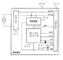
図8は、電源基板910の一構成例を示すブロック図である。電源基板910は、主基板31、表示制御基板80、音声制御基板70、ランプ制御基板35および賞球制御基板37等の制御基板と独立して設置され、遊技機内の各制御基板および機構部品が使用する電圧を生成する。この例では、AC24V、DC+30V、DC+21V、DC+12VおよびDC+5Vを生成する。また、バックアップ電源となるコンデンサ916は、DC+5Vすなわち各基板上のIC等を駆動する電源のラインから充電される。
【0067】
トランス911は、交流電源からの交流電圧を24Vに変換する。AC24V電圧は、コネクタ915に出力される。また、整流回路912は、AC24Vから+30Vの直流電圧を生成し、DC−DCコンバータ913およびコネクタ915に出力する。DC−DCコンバータ913は、+21V、+12Vおよび+5Vを生成してコネクタ915に出力する。コネクタ915は例えば中継基板に接続され、中継基板から各制御基板および機構部品に必要な電圧の電力が供給される。
【0068】
DC−DCコンバータ913からの+5Vラインは分岐してバックアップ+5Vラインを形成する。バックアップ+5Vラインとグラウンドレベルとの間には大容量のコンデンサ916が接続されている。コンデンサ916は、遊技機に対する電力供給が遮断されたときの各制御基板のバックアップRAMに対するバックアップ電源となる。また、+5Vラインとバックアップ+5Vラインとの間に、逆流防止用のダイオード917が挿入される。
【0069】
なお、バックアップ電源として、+5V電源から充電可能な電池を用いてもよい。電池を用いる場合には、+5V電源から電力供給されない状態が所定時間継続すると容量がなくなるような充電池が用いられる。
【0070】
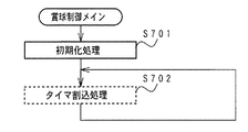
次に遊技機の動作について説明する。
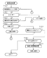
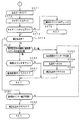
図9は、主基板31におけるCPU56の遊技制御処理を示すフローチャートである。図9(A)はCPU56が実行するメイン処理を示し、図9(B)は割込処理を示す。電源オン時のリセットが解けると、CPU56は、まず、クロックモニタ制御を動作可能状態にするために、内蔵されているクロックモニタレジスタをクロックモニタイネーブル状態に設定する(ステップS1)。クロックモニタ制御とは、入力されるクロック信号の低下または停止を検出すると、CPU56の内部で自動的にリセットを発生する制御である。次いで、CPU56は、初期化処理を行う(ステップS2)。なお、初期化処理では、所定期間後(例えば2ms後)にタイマ割込がかかるようにタイマの設定処理を行う。その後、停止図柄の種類を決定する乱数等の表示用乱数を更新する処理を繰り返し実行する(ステップS17)。
【0071】
図9(B)に示された処理は、CPU56内部のタイマ割込によって起動される。割込処理において、CPU56は、まず、所定期間後(例えば2ms後)に再度タイマ割込がかかるようにタイマの設定処理を行う(ステップS20)。
【0072】
次に、表示制御基板80に送出される表示制御コマンドをRAM55の所定の領域に設定する処理を行った後に(表示制御データ設定処理:ステップS4)、表示制御コマンドを出力する処理を行う(表示制御データ出力処理:ステップS5)。
【0073】
次いで、各種出力データの格納領域の内容を各出力ポートに出力する処理を行う(データ出力処理:ステップS6)。また、ホール管理用コンピュータに出力される大当り情報、始動情報、確率変動情報などの出力データを格納領域に設定する出力データ設定処理を行う(ステップS8)。さらに、パチンコ遊技機1の内部に備えられている自己診断機能によって種々の異常診断処理が行われ、その結果に応じて必要ならば警報が発せられる(エラー処理:ステップS9)。
【0074】
次に、遊技制御に用いられる大当り判定用の乱数等の各判定用乱数を示す各カウンタを更新する処理を行う(ステップS10)。
【0075】
次に、CPU56は、特別図柄プロセス処理を行う(ステップS11)。特別図柄プロセス制御では、遊技状態に応じてパチンコ遊技機1を所定の順序で制御するための特別図柄プロセスフラグに従って該当する処理が選び出されて実行される。そして、特別図柄プロセスフラグの値は、遊技状態に応じて各処理中に更新される。また、普通図柄プロセス処理を行う(ステップS12)。普通図柄プロセス処理では、7セグメントLEDによる可変表示器10を所定の順序で制御するための普通図柄プロセスフラグに従って該当する処理が選び出されて実行される。そして、普通図柄プロセスフラグの値は、遊技状態に応じて各処理中に更新される。
【0076】
さらに、CPU56は、スイッチ回路58を介して、ゲートセンサ12、始動口センサ17およびカウントセンサ23の状態を入力し、各入賞口や入賞装置に対する入賞があったか否か判定する(スイッチ処理:ステップS13)。CPU56は、さらに、停止図柄の種類を決定する乱数等の表示用乱数を更新する処理を行う(ステップS15)。
【0077】
また、CPU56は、賞球制御基板37との間の信号処理を行う(ステップS16)。すなわち、所定の条件が成立すると賞球制御基板37に賞球制御コマンドを出力する。賞球制御基板37に搭載されている賞球制御用CPUは、賞球制御コマンドに応じて玉払出装置97を駆動する。
【0078】
図10は、CPU56のINT処理を示すフローチャートである。上述したように、電源監視用IC902が電源電圧の低下を検出すると、CPU56に外部割込がかかる。また、図7に示されているように入力ポートに電源監視用IC902の出力が導入されている。
【0079】
電源電圧の低下にもとづくINT処理では、CPU56は、まず、レジスタの内容をバックアップRAMに転送する(ステップS31)。次いで、INTフラグをセットする(ステップS32)。INTフラグとは、電源電圧低下にもとづく割込が生じたことを示す内部フラグである。また、INTフラグは、バックアップRAM領域に設定される。CPU56は、さらに、RAMアクセスを禁止状態にして(ステップS33)、電源監視用IC902の出力が導入されている入力ポートのレベルを監視し続ける(ステップS34)。この状態で、電源電圧はさらに低下していき、遂には、CPU56の動作が停止する。
【0080】
しかし、入力ポートのレベルが通常時のレベルに復帰した場合には、CPU56は、RAMアクセスを許可状態にして(ステップS35)、バックアップRAMに保存されていたレジスタ値を本来のレジスタに復帰させる(ステップS36)。そして、INTフラグをリセットし(ステップS37)、割込がかかったアドレスに復帰する。
【0081】
このように、CPU56は、電源電圧が正常に復帰したことを検出すると、レジスタの状態を元に戻して割込がかかったアドレスに復帰する。従って、外部割込ライン(INTライン)にノイズ等がのった場合でも、制御を正常状態に復帰させることができる。
【0082】
図11は、図9に示されたメイン処理における初期化処理(ステップS2)の一例を示すフローチャートである。遊技機への電力供給が再開されると、初期リセット回路65からCPU56に初期リセット信号が入力される。CPU56は、初期リセット信号に応じてメイン処理を開始するのであるが、システムチェック処理において、まず、INTフラグがセットされているか否か確認する(ステップS42)。
【0083】
このとき、RAMアクセス許可状態に設定する必要があれば、すなわち、リセットがかけられたときに自動的にRAMアクセス許可状態にならないのであれば、CPU56は、RAMアクセス許可状態に設定する。
【0084】
INTフラグがセットされていなければ、レジスタおよびRAM領域を全てクリアし(ステップS46)、必要な初期値を設定する(ステップS47)。そして、電源投入時画面表示コマンド送出要求をセットし(ステップS48)、スタックポインタを初期化して(ステップS49)、初期化処理を終了する。
【0085】
なお、電源投入時画面表示コマンド送出要求がセットされると、例えば、図9に示された表示制御データ出力処理(ステップS5)によって電源投入時画面表示コマンドが表示制御基板80に送出される。表示制御基板80における表示制御用CPU101は、電源投入時画面表示コマンドを受信すると、可変表示部9に、電源投入時に表示される画面としてあらかじめ決められている画面を表示する。
【0086】
ステップS42でINTフラグがセットされていることが確認されると、CPU56は、バックアップRAMに保存されていたレジスタ値を本来のレジスタに復帰させる(ステップS43)。そして、INTフラグをリセットし(ステップS44)、エラー画面表示コマンド送出要求をセットする(ステップS45)。
【0087】
なお、エラー画面表示コマンド送出要求がセットされると、例えば、表示制御データ出力処理(ステップS5)によってエラー画面表示コマンドが表示制御基板80に送出される。表示制御基板80における表示制御用CPU101は、エラー画面表示コマンドを受信すると、可変表示部9にあらかじめ決められているエラー画面を表示する。
【0088】
そして、CPU56は、スタックポインタが指すスタックエリアの値をジャンプ先としてそこにジャンプする。スタックポインタは、レジスタの一つであるから、ステップS43の処理によって、電源断したときの値に復元されている。また、この実施の形態では、スタックエリアはバックアップRAM領域に形成されている。すなわち、電源断中でも保存されている。従って、制御状態は、電源断時の状態に戻る。
【0089】
例えば、電源断時に、表示制御基板80における表示制御用CPU101が可変表示部9において図柄変動表示を行っていたとする。すると、電源復旧時に、表示制御用CPU101は、エラー画面表示コマンドを受信するので、可変表示部9にエラー画面を表示する。一方、主基板31のCPU56は、電源断時の状態すなわち特別図柄変動中の遊技状態に戻る。そして、特別図柄変動中の遊技状態が終了すると、図柄停止を示すコマンドや大当り表示を示すコマンドを送出する。表示制御用CPU101は、その段階で、エラー表示を停止して、続く表示制御を続行することができる。
【0090】
以上のように、CPU56は、復帰時にINTフラグがセットされていたらデータ復帰処理を行い、INTフラグがセットされていなければ通常の初期設定処理(ステップS46,S47)を行う。そして、データ復帰処理では、保存されていたレジスタの復帰処理とINTフラグのリセット処理とが行われる。また、電源バックアップされているRAM領域におけるスタックエリアに保存されていた復帰アドレスに戻るので、遊技制御手段は、電源断時の遊技状態に復帰することができる。
なお、この実施の形態では、電源監視用IC902からの信号が外部割込端子に入力されたが、マスク不能割込端子(NMI端子)にその信号を導入し、NMI割込処理で上記の電源断時の処理を行ってもよい。
【0091】
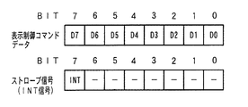
図12は、表示制御コマンドの構成例を示す説明図である。図12に示すように、表示制御コマンドは、8ビットのデータと、1ビットのストローブ信号(INT信号)とから構成されている。
【0092】
図13は、8ビットのデータによる表示制御コマンドデータの構成例を示す説明図である。図13に示すように、例えば、8ビットのうちの上位4ビットで制御の種類を指示し、下位4ビットで具体的制御内容を指示する。例えば、この例では、上位4ビットが[0,0,0,1]であれば、下位4ビットの数値でリーチ種類や全図柄停止等が指示される。また、上位4ビットが[1,0,0,0],[1,0,0,1]または[1,0,1,0]であれば、下位4ビットの数値で可変表示部9に可変表示される左図柄、中図柄または右図柄の停止図柄が指示される。
【0093】
また、上位4ビットが[1,1,0,1]であればエラー画面表示要求コマンドであることを示す。上位4ビットが[1,1,1,1]であれば電源投入時画面表示要求コマンドであることを示す。なお、それらのコマンドにおいて下位4ビットは例えば0に設定される。
【0094】
図14はCPU56が実行する特別図柄プロセス処理のプログラムの一例を示すフローチャートである。図14に示す特別図柄プロセス処理は、図9のフローチャートにおけるステップS11の具体的な処理である。CPU56は、特別図柄プロセス処理を行う際に、特別図柄プロセスフラグの値に応じて、図14に示すステップS300〜S309のうちのいずれかの処理を行う。各処理において、以下のような処理が実行される。
【0095】
特別図柄変動待ち処理(ステップS300):始動入賞口14(この実施の形態では可変入賞球装置15の入賞口)に打球入賞して始動口センサ17がオンするのを待つ。始動口センサ17がオンすると、始動入賞記憶数が満タンでなければ、始動入賞記憶数を+1するとともに大当り判定用乱数を抽出する。
【0096】
特別図柄判定処理(ステップS301):特別図柄の可変表示が開始できる状態になると、始動入賞記憶数を確認する。始動入賞記憶数が0でなければ、抽出されている大当り判定用乱数の値に応じて大当りとするかはずれとするか決定する。
停止図柄設定処理(ステップS302):左右中図柄の停止図柄を決定する。
【0097】
リーチ動作設定処理(ステップS303):リーチ判定用乱数の値に応じてリーチ動作するか否か決定するとともに、リーチ動作用乱数の値に応じてリーチ動作の変動態様を決定する。
【0098】
全図柄変動開始処理(ステップS304):可変表示部9において全図柄が変動開始されるように制御する。このとき、表示制御基板80に対して、左右中最終停止図柄と変動態様を指令する情報とが送信される。また、可変表示部9に背景やキャラクタも表示される場合には、それに応じた表示制御コマンドデータが表示制御基板80に送出されるように制御する。
【0099】
全図柄停止待ち処理(ステップS305):所定時間が経過すると、可変表示部9において表示される全図柄が停止されるように制御する。また、全図柄停止のタイミングまで、所定のタイミングで左右図柄が停止されるように制御する。
【0100】
大当り表示処理(ステップS306):停止図柄が大当り図柄の組み合わせである場合には、大当り表示の表示制御コマンドデータが表示制御基板80に送出されるように制御するとともに内部状態(プロセスフラグ)をステップS307に移行するように更新する。そうでない場合には、内部状態をステップS309に移行するように更新する。なお、大当り図柄の組み合わせは、左右中図柄が揃った組み合わせである。また、遊技制御基板80の表示制御用CPU101は表示制御コマンドデータに従って、可変表示部9に大当り表示を行う。大当り表示は遊技者に大当りの発生を報知するためになされるものである。
【0101】
大入賞口開放開始処理(ステップS307):大入賞口を開放する制御を開始する。具体的には、カウンタやフラグを初期化するとともに、ソレノイド21を駆動して大入賞口を開放する。
【0102】
大入賞口開放中処理(ステップS308):大入賞口ラウンド表示の表示制御コマンドデータが表示制御基板80に送出する制御や大入賞口の閉成条件の成立を確認する処理等を行う。大入賞口の閉成条件が成立したら、大当り遊技状態の終了条件が成立していなければ内部状態をステップS307に移行するように更新する。大当り遊技状態の終了条件が成立していれば、内部状態をステップS309に移行するように更新する。
【0103】
大当たり終了処理(ステップS309):大当たり遊技状態が終了したことを遊技者に報知するための表示を行う。その表示が終了したら、内部フラグ等を初期状態に戻し、内部状態をステップS300に移行するように更新する。
【0104】
上記の各ステップの処理に応じて、遊技制御プログラム中の表示制御コマンドを送出する処理を行うモジュール(図9におけるステップS5)は、対応する表示制御コマンドデータを出力ポートに出力するとともにストローブ信号をオン状態にする。
【0105】
上記の実施の形態では、電源断時にCPU56は、各レジスタの内容をバックアップRAMに保存したが、電源復旧時に所定の復帰制御を行えば、そのようなレジスタ保存制御を行わなくてもよい。図15および図16は、電源断時に各レジスタの内容をバックアップRAMに保存しない形態における制御を示すフローチャートである。
【0106】
図15は、INT処理を示すフローチャートである。この場合には、CPU56は、まず、INTフラグをセットする(ステップS32)。また、RAMアクセスを禁止状態にして(ステップS33)、電源監視用IC902の出力が導入されている入力ポートのレベルを監視し続ける(ステップS34)。
【0107】
入力ポートのレベルが通常時のレベルに復帰した場合には、CPU56は、RAMアクセスを許可状態にして(ステップS35)、INTフラグをリセットし(ステップS37)、割込がかかったアドレスに復帰する。
【0108】
図16は、メイン処理における初期化処理を示すフローチャートである。この場合には、CPU56は、まず、INTフラグがセットされているか否か確認する(ステップS42)。セットされていなければ、レジスタおよびRAM領域を全てクリアし(ステップS46)、必要な初期値を設定する(ステップS47)。そして、電源投入時画面表示コマンド送出要求をセットし(ステップS48)、スタックポインタを初期化して(ステップS49)、初期化処理を終了する。
【0109】
この実施の形態では、特別図柄プロセスフラグが、バックアップRAM領域に形成されている。ステップS42でINTフラグがセットされていることが確認されると、CPU56は、バックアップされている特別図柄プロセスフラグの値を読み出し、そのときの値(遊技状態を示す)から、そのときの遊技状態における各レジスタ状態を復元する(ステップS50)。そして、INTフラグをリセットし(ステップS44)、スタックポインタが指すスタックエリアの値をジャンプ先としてそこにジャンプする。なお、この実施の形態では、汎用の各レジスタの値を電源断時にバックアップRAMに保存する必要はないが、スタックポインタは保存される必要がある。なお、可変表示器10に可変表示される普通図柄の変動制御において用いられる普通図柄プロセスフラグも、バックアップRAM領域に形成されていることが好ましい。
【0110】
以上のように、この例では、遊技状態に応じて選択的に処理を行うためのフラグである特別図柄プロセスフラグが遊技機に対する電源断時にも保存され、データ復帰処理において、保存されていた特別図柄プロセスフラグの値に応じて遊技状態を復元する。
【0111】
例えば、電源断時に、表示制御基板80における表示制御用CPU101が可変表示部9において図柄変動表示を行っていたとする。すると、電源復旧時に、CPU56は、特別図柄プロセスフラグの値に応じて、電源断時に行っていた図柄変動開始時の遊技状態に復帰することができる。その段階で、図柄変動を開始させるための表示制御コマンドが表示制御基板80に対して送出されるので、表示制御用CPU101は、図柄の変動を図柄変動開始時の状態から再度実行することになる。
【0112】
図17は、主基板31から賞球制御基板37に送信される賞球制御コマンドのビット構成を示す説明図である。図17に示すように、1バイト中の上位4ビットが制御指定部として使用され、下位4ビットが賞球数を示す領域として用いられる。
【0113】
図18に示すように、制御指定部において、ビット7,6,5,4が「0,1,0,0」であれば払出個数指定コマンドであることを示し、「0,1,0,1」であれば払出指定コマンドであることを示す。払出個数指定コマンドは、主基板31のCPU56が入賞を検出すると直ちに賞球制御基板37に送出される。
【0114】
ビット7,6,5,4が「1,0,0,0」である球切れ指定コマンドは、玉切れ検出スイッチ167または玉切れスイッチ187がオンしたとき(玉切れ状態フラグがオンしたとき)に、主基板31から送信される。また、ビット7,6,5,4が「1,0,0,1」である発射停止指定コマンドは、余剰玉受皿4が満タンになって満タンスイッチ48がオンしたとき(満タン状態フラグがオンしたとき)に、主基板31から送信される。
【0115】
賞球制御コマンドは、主基板31から賞球制御基板37に、1バイト(8ビット:賞球制御コマンドD7〜D0)のデータとして出力される。賞球制御コマンドD7〜D0は正論理で出力される。また、賞球制御コマンドD7〜D0が出力されたときには、負論理の賞球制御INT信号が出力される。
【0116】
図6に示されたように、賞球制御コマンドは、出力ポート577を介して送信される。そして、この実施の形態では、図19に示すように、主基板31から賞球制御コマンドD7〜D0が出力されるときに、賞球制御INT信号が5μs以上ローレベルになる。賞球制御INT信号は、賞球制御基板37において、賞球制御用CPU371の割込端子に接続されている。よって、賞球制御用CPU371は、割り込みがあると、賞球制御コマンドD7〜D0が主基板31から送出されたことを認識でき、割込処理において賞球制御コマンド受信処理を行う。
【0117】
なお、図17に示されたコマンド構成は一例であって、他の構成にしてもよい。例えば、1バイト中の上位下位を、図17に示された構成とは逆にしてもよい。また、この実施の形態では、主基板31から賞球制御基板37に送出される全ての賞球制御コマンドは、同一の8本の信号線(D7〜D0)で転送される。よって、コマンド数が増えても配線数は増えない。そして、図17に示すように、1つの表示制御コマンドには、賞球数を示すデータ部と制御指定部とを含む。よって、賞球制御基板37の賞球制御用CPU371は、コマンドを受信したら直ちにどのような制御指令を受けたのか認識することができる。
【0118】
図20は、電源監視および電源バックアップのための賞球制御用CPU371周りの一構成例を示すブロック図である。図20に示すように、電源監視用IC932は、+30V電圧を導入し、+30V電圧を監視することによって電源断の発生を検出する。具体的には、+30V電圧が所定値(例えば+30Vの80%)以下になったら、電源断が生ずるとして、賞球制御用CPU371に割り込み信号を与える。賞球制御用CPU371において、この割り込みは、マスク不能割込(NMI)端子に入力されている。また、NMI端子に入力される信号は、入力ポートにも入力されている。従って、賞球制御用CPU371は、NMI処理において、入力ポートのレベルを確認することによって電源断の状況を確認することができる。
【0119】
電源監視用IC932が電源断を検知するための所定値は、通常時の電圧より低いが、賞球制御用CPU371が暫くの間動作しうる程度の電圧である。また、電源監視用IC932が、賞球制御用CPU371が必要とする電圧(この例では+5V)よりも高い電圧を監視するように構成されているので、賞球制御用CPU371が必要とする電圧に対して監視範囲を広げることができる。従って、より精密な監視を行うことができる。
【0120】
+5V電源から電力が供給されていない間、賞球制御用CPU371の内蔵RAMの少なくとも一部は、電源基板から供給されるバックアップ電源がバックアップ端子に接続されることによってバックアップされ、遊技機に対する電源が断しても内容は保存される。そして、+5V電源が復旧すると、初期リセット回路935からリセット信号が発せられるので、賞球制御用CPU371は、通常の動作状態に復帰する。そのとき、必要なデータがバックアップされているので、停電等からの復旧時には停電発生時の遊技状態に復帰することができる。
【0121】
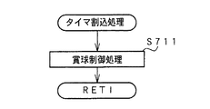
図21は、賞球制御用CPU371のメイン処理を示すフローチャートである。メイン処理では、賞球制御用CPU371は、まず、RAM領域をクリアする等の初期値設定処理を行う(ステップS701)。なお、内蔵RAMの電源バックアップされたRAM領域(バックアップ領域)にデータが設定されている場合には、それらの領域のクリア処理はなされない。その後、この実施の形態では、賞球制御用CPU371は、所定期間(例えば2ms)毎に発生するタイマ割込による割込処理で賞球払出制御を行う(ステップS702)。タイマ割込処理では、図22に示すように、賞球制御用CPU371は、賞球払出制御処理を実行する(ステップS711)。
【0122】
図23は、賞球制御基板37におけるバックアップRAMに形成される各カウンタを示す説明図である。図23に示すように、1個カウンタ〜15個カウンタが用意されている。各個数カウンタは、主基板31のCPU56すなわち遊技制御手段から受信した払出個数を示す各払出個数指示コマンドに対応している。例えば、15個の賞球払出を指示する払出個数指示コマンドを受信したら15個カウンタの値が+1される。また、この実施の形態では、6個カウンタ、10個カウンタおよび15個カウンタのみが使用されるが、このように他種類の個数に応じたカウンタを用意しておけば、入賞に応じた賞球数が異なる他の遊技にも容易に賞球制御手段を流用することができる。
【0123】
なお、賞球制御用CPU371が使用するワークエリアの全てが電源バックアップされている必要はない。少なくとも、図23に示された各カウンタと後述するフラグ類またはレジスタのデータ退避のアドレスがバックアップRAM領域に形成されていればよい。
【0124】
図24〜図30は、賞球制御用CPU371が実行する賞球払出制御処理を示すフローチャートである。なお、この実施の形態では、賞球払出制御処理はタイマ割込処理で実行されるように構成されているが、そのような構成ではなく、通常の処理(割込処理ではない)によって実行されるように構成してもよい。
【0125】
賞球払出制御処理において、賞球制御用CPU371は、賞球制御コマンドが受信されているか否か確認する(ステップS480)。受信されていれば、ステップS511に移行する。受信されていなければ、現在エラー状態中であるか否か確認する(ステップS481)。エラー状態中であればエラー処理を行う。エラー状態中でない場合には、賞球中(または補正払出中)であるか否か確認する(ステップS482)。賞球中でない場合には、玉貸し処理中であるか否か確認する(ステップS483)。玉貸し中であれば、玉貸し中の処理に移行する。
【0126】
玉貸し中でもなければ、全ての個数カウンタの値が0であるか否か確認する(ステップS484)。全て0であれば、すなわち、賞球払出を行う必要がない場合には、遊技機の外部機器としてのカードユニット50からの玉貸し要求信号であるBRQ信号がオンになっているかどうか確認する(ステップS491)。
【0127】
なお、ここでは、遊技制御手段から通知された賞球指示に対して、賞球対応に設けられた個数カウンタに賞球回数を記憶するようにしたが、1つのカウンタを用意し、遊技制御手段から通知された賞球数をそのカウンタに加算するようにしてもよい。
【0128】
BRQ信号がオンになっていれば、玉貸し開始のための処理を行って(ステップS492)、玉貸し中の処理に移行する。なお、玉貸し制御のためのカウンタも、バックアップRAM領域に形成されていることが好ましい。
【0129】
ステップS484において、個数カウンタの全てが0になっていなければ、ステップS500の処理を行う。
【0130】
ステップS500において、補正払出フラグがオンしていれば、すなわち、補正払出をすべきことに決定されていた場合には、ステップS507に移行する。補正払出フラグがオンしていなければ、賞球制御用CPU371は、全ての個数カウンタ(この例では15個カウンタ〜1個カウンタ)について、個数の多いものから順にカウンタ値をチェックする(ステップS501)。そして、値が0でない個数カウンタに対応した個数を払出個数カウンタに設定する(ステップS503)。さらに、賞球処理中フラグをオンし(ステップS503)、払出モータ289をオンする(ステップS507)。そして、賞球払出中処理に移行する。
【0131】
賞球制御コマンド(払出個数指示コマンド)を受信した場合には、ステップS511の処理が開始される。ステップS511において、賞球制御用CPU371は、払出個数指示コマンドで指示された個数に対応した個数カウンタの値を+1する(ステップS512)。
【0132】
以上のように、賞球制御基板37に搭載された賞球制御用CPU371は、主基板31のCPU56から送られた払出個数指示コマンドに含まれる賞球数をバックアップRAM領域に記憶する。
【0133】
なお、賞球制御コマンドには払出個数指示コマンド以外のコマンドもあるが、図26では、それらのコマンドの受信処理は省略されている。
【0134】
以上のように、賞球制御処理では、ステップS511以降の処理で、遊技制御手段から払出個数指示コマンドを受信していれば、対応する個数カウンタが+1される。すると、次回の賞球制御処理起動時に、ステップS484でそのことが検出され、ステップS500以降の処理で払出個数カウンタに所定値が設定されるとともに、賞球処理中とされる。そして、次回の賞球制御処理起動時に、賞球処理中であることが検出され、ステップS532以降の賞球払出中の処理が実行される。
【0135】
図24に示されているように、ここでは、コマンド受信順に関わらず賞球個数の多い払出指示を優先させたが、賞球個数の少ない順に処理してもよい。また、コマンドを受信した順に、対応する賞球処理を開始してもよい。なお、賞球数の多い順に払出処理を行う場合には、遊技者に対して遊技球が速く補給されることになるので、遊技者が不必要に玉借りを行う機会が減る。すなわち、遊技者にとって有利な遊技環境を提供することができる。
【0136】
ステップS532以降の処理は賞球払出中の処理である。賞球払出中の処理において、まず、状態チェックが行われる(ステップS532)。賞球制御用CPU371は、払出モータ位置センサおよび賞球カウントスイッチ301Aを監視することによって賞球払出が正常に行われているか否かチェックする。状態チェックとは、現在、払出モータ位置センサのオンを監視している状態にあるのか、払出モータ位置センサのオフを監視している状態にあるのかを判定する処理である。
【0137】
この実施の形態では、払出モータ位置センサおよび賞球カウントスイッチ301Aの監視のために、以下のタイマを用いる。
(1)タイマT11:払出モータ位置センサのオン監視用
(2)タイマT12:払出モータ位置センサのオフ監視用
(3)タイマT13:賞球カウントスイッチ301Aのオン監視用
(4)タイマT14:賞球カウントスイッチ301Aのオフ監視用
【0138】
また、払出モータ位置センサによって払出個数が確認されてから、賞球カウントスイッチ301Aが実際の払出球を検出するまでに遊技球数個分の流下に要する遅れ時間があり、その時間を待つために以下のタイマを用いる。
(5)タイマT15:最後の払出球が払出モータ位置センサによって確認されてから、その球が賞球カウントスイッチ301Aを通過するまでの時間待ち用
【0139】
ここでは、それらのタイマが動作中であることを確認することによって状態チェックを行う。ステップS532では、タイマT11が動作中であるときには、払出モータ位置センサのオン待ち処理(ステップS534)に移行し、タイマT12が動作中であるときには、払出モータ位置センサのオフ待ち処理(ステップS542)に移行する。タイマ15が動作中であるときには、タイマ15のタイムアウト待ち(ステップS573)に移行する。いずれのタイマも動作中でないときには、タイマT11をスタートさせる(ステップS533)。
【0140】
ステップS534において、賞球制御用CPU371は、払出モータ位置センサがオンするのを待つ。オンする前にタイマT11がタイムアウトするとエラー処理に移行する(ステップS535,S536)。払出モータ位置センサがオンすると、タイマT11を停止して(ステップS537)、タイマT12を起動する(ステップS541)。その後、賞球制御用CPU371は、払出モータ位置センサがオフするのを待つ(ステップS542)。オフする前にタイマT12がタイムアウトするとエラー処理に移行する(ステップS543,S545)。なお、タイマT11,T12がタイムアウトしていない間、賞球カウントスイッチチェックサブルーチンを実行する(ステップS547)。
【0141】
払出モータ位置センサがオフすると、タイマT12を停止して(ステップS546)、払出個数カウンタを−1する(ステップS551)。そして、賞球制御用CPU371は、払出個数カウンタの値が0になったか否か確認する(ステップS552)。0になったことは、所定個数について払出制御を行ったことを意味する。そこで、補正払出中でなければ(ステップS553)、今回の賞球払出個数に対応した個数カウンタ(15個カウンタ〜1個カウンタのいずれか)の値を−1する(ステップS554)。さらに、払出モータ289を停止するとともに(ステップS571)、タイマT15を起動する(ステップS572)。
【0142】
その後、タイマT15のタイムアウトを待つ(ステップS573)。タイムアウトしていない間、賞球カウントスイッチチェックサブルーチンを実行する(ステップS574)。
【0143】
タイマT15がタイムアウトすると、補正払出中でなければ(ステップS574)、今回の賞球払出の個数と賞球数カウンタの値を比較する(ステップS575)。
【0144】
なお、賞球数カウンタは、賞球カウントスイッチチェックサブルーチンで、払出モータ位置センサの下部に位置する賞球カウントスイッチ301Aの1回のオンが検出される度にカウントアップされる。タイマT15がタイムアウトしたとき、玉払出が正常に行われていれば、賞球数カウンタの値は、払出モータ位置センサのオン回数に一致する。例えば、15個賞球が行われていたときには、払出モータ位置センサのオン回数が15になると、ステップS552で払出個数カウンタの値が0になり、その後、T15の時間だけ経過すると賞球数カウンタの値が15になるはずである。
【0145】
ステップS575の判断結果が不一致の場合には、賞球不足数(賞球予定数−賞球数カウンタ値)を補正個数カウンタに設定し(ステップS583)、払出モータ289をオンし(ステップS584)、補正払出中フラグをオンする(ステップS585)。なお、賞球不足数は補正予定数として記憶される。
【0146】
補正払出が行われていた場合には、賞球数カウンタの値が補正予定数と一致しているか否か確認し(ステップS581)、一致していなければ、ステップS586に移行する。一致していれば、補正払出中フラグをリセットして(ステップS582)、この回の処理を終了する。
【0147】
ステップS575の判断結果が一致であった場合には、全ての個数カウンタが0になっているか確認し(ステップS586)、0になっていれば、賞球処理中フラグをリセットして(ステップS587)、この回の処理を終了する。
【0148】
以上のように、賞球制御用CPU371は、払出個数カウンタの値によって、所定個の賞球が完了したか否か認識し、完了したら対応する個数カウンタの値を−1する。そして、所定時間経過後に、賞球カウントスイッチ301Aによる検出回数を確認し、賞球カウントスイッチ301Aを通過した遊技球数が予定払出数に満たないことを検出した場合には補正払出処理を開始する。
【0149】
なお、各個数カウンタおよび払出個数カウンタはバックアップRAM領域に形成されているので、停電等による電源断が生じても保存される。また、賞球中を示すフラグもバックアップRAM領域に形成される。よって、停電等からの復旧時に、賞球制御用CPU371は、保存されているデータにもとづいて賞球払出制御を継続することができる。すなわち、停電からの復旧時に、賞球中を示すフラグが設定されていることを検知して、賞球制御用CPU371は、直ちに、賞球払出処理を再開することができる。
【0150】
さらに、補正個数カウンタ等もバックアップRAM領域に形成されている。また、補正払出中を示すフラグもバックアップRAM領域に形成される。よって、補正払出処理中に停電等が生じても、停電等からの復旧時に、賞球制御用CPU371は、保存されているデータにもとづいて補正払出制御を継続することができる。
【0151】
なお、フラグ類がバックアップRAM領域に設定されていなくても、個数カウンタがバックアップRAM領域に設定されていれば、賞球制御用CPU371は、電源復旧時に、各個数カウンタの設定値をチェックすることによって、未払出賞球があるか否かを検出することができる。そして、未払出賞球があることを検出した場合には、例えば、賞球払出中フラグをセットすることによって賞球払出処理を再開することができる。
【0152】
図30は、賞球カウントスイッチチェックサブルーチンを示すフローチャートである。賞球カウントスイッチチェックにおいて、まず、状態チェックが行われる(ステップS511)。ステップS511において、タイマT13が動作中であるときには、賞球カウントスイッチ301Aのオン待ち処理(ステップS513)に移行し、タイマT14が動作中であるときには、賞球カウントスイッチ301Aのオフ待ち処理(ステップS518)に移行する。いずれのタイマも動作中でないときには、タイマT13をスタートさせる(ステップS512)。
【0153】
そして、賞球カウントスイッチ301Aがオンするのを待つ(ステップS513)。賞球カウントスイッチ301Aの出力がオンする前にタイマT13がタイムアウトするとエラー処理に移行する(ステップS514,S515)。
【0154】
賞球カウントスイッチ301Aの出力がオン状態になると、タイマT13を停止して(ステップS516)、タイマT14を起動する(ステップS517)。そして、賞球カウントスイッチ301Aがオフするのを待つ(ステップS518)。賞球カウントスイッチ301Aがオフする前にタイマT14がタイムアウトするとエラー処理に移行する(ステップS519,S520)。タイマT14がタイムアウトする前に賞球カウントスイッチ301Aがオフした場合には、タイマT14を停止する(ステップS521)。そして、賞球数カウンタの値を+1する(ステップS522)。
【0155】
なお、この実施の形態では、遊技制御手段から通知された賞球指示に対して、賞球対応に設けられた個数カウンタに賞球回数が記憶されたが、1つのカウンタを有し、遊技制御手段から通知された賞球数をカウンタに加算するようにしてもよい。そのように構成されている場合には、カウンタ個数が減るとともに、バックアップすべきRAM領域を小さくすることができる。
【0156】
また、この実施の形態では、払出モータ289を駆動しているときに、所定時間内に払出モータ位置センサがオンしなかったりオフしなかった場合には、エラーと判定される。払出モータ位置センサがオンしなかったりオフしなかった場合には、玉詰まりが生じている場合等が考えられるからである。
【0157】
さらに、払出モータ位置センサの出力が正常であるにも関わらず、センサよりも下部に設けられている賞球カウントスイッチがオンしなかった場合には、賞球カウントスイッチ301Aの故障等が考えられるので、やはりエラーと判定される。そして、賞球カウントスイッチ301Aがオフしなかった場合には、賞球カウントスイッチ301Aの近傍の玉誘導路で玉詰まりが生じている等が考えられるので、やはりエラーと判定される。
【0158】
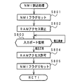
図31は、賞球制御用CPU371が実行するNMI割込処理を示すフローチャートである。この場合には、賞球制御用CPU371は、まず、NMIフラグをセットする(ステップS801)。また、RAMアクセスを禁止状態にして(ステップS802)、電源監視用IC932の出力が導入されている入力ポートのレベルを監視し続ける(ステップS803)。
【0159】
入力ポートのレベルが通常時のレベルに復帰した場合には、賞球制御用CPU371は、RAMアクセスを許可状態にして(ステップS804)、NMIフラグをリセットし(ステップS805)、NMI割込がかかったアドレスに復帰する。
【0160】
このように、賞球制御用CPU371は、電源電圧が正常に復帰したことを検出すると、レジスタの状態を元に戻してNMI割込がかかったアドレスに復帰する。従って、NMIラインにノイズ等がのった場合でも、制御を正常状態に復帰させることができる。
【0161】
図32は、賞球制御用CPU371が実行するメイン処理における初期化処理を示すフローチャートである。この場合には、賞球制御用CPU37は、まず、電源投入時か否か確認する(ステップS811)。電源投入時であるか否かは、例えば、電源バックアップされていないRAMの内容が破壊されているか否かによって判定される。つまり、電源バックアップされていないRAMの内容が破壊されていれば電源投入時であると判定できる。このとき、RAMアクセス許可状態に設定する必要があれば、すなわち、リセットがかけられたときに自動的にRAMアクセス許可状態にならないのであれば、賞球制御用CPU371は、RAMアクセス許可状態に設定する。
【0162】
電源投入時であれば、賞球制御用CPU37は、NMIフラグがセットされているか否か確認する(ステップS812)。セットされていなければ、レジスタおよびRAM領域を全てクリアし(ステップS814)、必要な初期値を設定する(ステップS815)。そして、スタックポインタを初期化して(ステップS816)、初期化処理を終了する。
【0163】
ステップS812でNMIフラグがセットされていることが確認されると、CPU56は、NMIフラグをリセットし(ステップS813)、スタックポインタが指すスタックエリアの値をジャンプ先としてそこにジャンプする。なお、この実施の形態では、汎用の各レジスタの値を電源断時にバックアップRAMに保存する必要はないが、スタックポインタは保存される必要がある。また、スタックエリアはバックアップRAM領域に形成されているので、賞球制御用CPU371は、電源投入時にNMIフラグがセットされていることを検出することによって、確実に電源断時の制御状態に戻ることができる。
【0164】
例えば、賞球中フラグがバックアップRAM領域に形成されていれば、賞球中を示すフラグが設定されていることを検知して、賞球制御用CPU371は、直ちに、バックアップRAM領域に保存されている各個数カウンタの値にもとづいて賞球払出処理を再開することができる。
【0165】
フラグ類がバックアップRAM領域に設定されていなくても、個数カウンタがバックアップRAM領域に設定されていれば、賞球制御用CPU371は、電源復旧時に、遊技状態記憶の読み出し処理を行って、すなわち、各個数カウンタの設定値を読み出して、未払出賞球があるか否かを検出することができる。そして、未払出賞球があることを検出した場合には、例えば、賞球払出中フラグをセットすることによって賞球払出処理を再開することができる。
【0166】
図33は、賞球制御用CPU371が実行するNMI割込処理の他の例を示すフローチャートである。この場合には、賞球制御用CPU371は、まず、未払出賞球個数または未払出玉貸し個数が記憶されているか否か確認する(ステップS821)。そのような記憶があれば、NMIフラグをセットする(ステップS822)。また、RAMアクセスを禁止状態にして(ステップS823)、電源監視用IC932の出力が導入されている入力ポートのレベルを監視し続ける(ステップS803)。
【0167】
入力ポートのレベルが通常時のレベルに復帰した場合には、賞球制御用CPU371は、RAMアクセスを許可状態にして(ステップS804)、NMIフラグをリセットし(ステップS805)、NMI割込がかかったアドレスに復帰する。
【0168】
未払出賞球個数または未払出玉貸し個数の記憶がない場合には、RAMアクセスを禁止状態にして(ステップS823)、ステップS803に移行する。このような制御によれば、未払出状態のときに電源断が生じた場合にのみ、すなわち、必要な場合にのみ、電源復旧時の制御状態復帰のための準備が行われる。
【0169】
なお、ここでは、賞球制御用CPU371のNMI端子に電源電圧が低下したことを示す信号を導入したが、外部割込端子にその信号を導入し、マスク可能な割込処理によって上記の電源断時の処理を行ってもよい。また、賞球制御用CPU371のみならず、他の制御基板に搭載されているCPUについても、賞球制御用CPU371と同様の電源断時処理を行わせるようにしてもよい。
【0170】
【発明の効果】
以上のように、本発明によれば、遊技機を、電源電圧監視手段からの検出信号が、遊技用装置制御マイクロコンピュータの割込端子に入力され、遊技用装置制御マイクロコンピュータが、電源電圧監視手段からの検出信号が割込端子に入力されたことに応じて、遊技制御処理を実行する状態から割込処理を実行する状態に移行し、該割込処理において遊技状態記憶を保持することが可能な揮発性記憶手段にスタックポインタを退避するデータ退避処理を行うとともにデータ退避処理を行ったことを示すデータ退避フラグを揮発性記憶手段にセットし、遊技状態記憶は、スタックポインタが指すスタックエリアに保存されている復帰アドレスと、遊技状態に応じて所定の順序で選択的に実行される複数の処理のうちいずれの処理を実行するのかを示すプロセスフラグとを含み、複数の処理は、プロセスフラグに従って実行される処理であって入賞領域のうちの始動領域に遊技球が入賞したことに応じて実行される図柄の可変表示を開始させる処理を含み、遊技機に電源が投入されたときに、データ退避フラグがセットされていることを条件に、遊技状態を復帰させ、表示制御用マイクロコンピュータに復帰時に表示されるあらかじめ決められている画面の表示要求コマンドを送信するデータ復帰処理を行うとともに、プログラムの実行アドレスをスタックエリアに保存されている復帰アドレスに復帰させて、電源監視手段が検出信号を出力したときに識別情報の変動中であれば識別情報の変動中の状態に戻り、遊技機に電源が投入されたときに、データ退避フラグがセットされていないときには、あらかじめ定められている値をレジスタに設定し、表示制御用マイクロコンピュータに初期化時に表示されるあらかじめ決められている画面の表示要求コマンドを送信する初期設定処理を行い、識別情報の変動が終了したときに、大当り遊技状態に制御するときには大当り表示を示すコマンドを表示制御用マイクロコンピュータに送信し、賞球制御マイクロコンピュータは、遊技機に電源が投入されたときに、該賞球制御マイクロコンピュータに内蔵されている揮発性記憶手段に払出予定数を示すデータが保存されていると判定したときには球払出装置に遊技球を払い出させる処理を継続して実行し、表示制御用マイクロコンピュータは、初期化時に表示されるあらかじめ決められている画面の表示要求コマンドを受信したことに応じて可変表示装置に当該画面を表示する制御を行い、復帰時に表示されるあらかじめ決められている画面の表示要求コマンドを受信したことに応じて可変表示装置に当該画面を表示する制御を行い、可変表示装置に復帰時に表示されるあらかじめ決められている画面を表示しているときに、遊技用装置制御マイクロコンピュータから大当り表示を示すコマンドを受信したときに当該画面の表示を終了させるように構成したので、データ退避処理を行ったことを示すフラグのオンオフに応じてデータ復帰処理を行うか否か判断することができ、保存されていたデータを電源復帰後に確実に活用することができる効果がある。また、電源復旧時に、正確に電源断時の状態に戻ることができる。
【0171】
データ退避のトリガとなる信号が入力する割込端子がマスク可能割込端子である場合には、優先度の高いマスク不能割込端子への信号にもとづくマスク不能割込を他の緊急処理で使用することができ、例えば、遊技制御において緊急性を要する制御のためにマスク不能割込を割り当てることができる。
【0172】
遊技用装置制御マイクロコンピュータが、データ復帰処理にて、少なくとも、データ退避フラグのリセット処理と、遊技状態の復元を行うための遊技状態記憶の読み出し処理とを行うように構成されていることから、遊技状態記憶の読み出し処理によって制御状態を電源断時の状態に確実に戻すことができ、遊技者に不利益を与えないようにすることができる。
【0178】
電源電圧監視手段からの検出信号は、遊技用装置制御マイクロコンピュータの入力ポートにも入力され、遊技用装置制御マイクロコンピュータが、入力ポートに入力された検出信号が正常状態を示すレベルに復帰したらデータ退避フラグをリセットして、遊技制御処理を実行する状態に戻るように構成されていることから、電源電圧が一時的電圧低下しても正常に復帰すると、レジスタの状態を元に戻して割込がかかったアドレスに復帰することができる。
【0179】
電源基板が、遊技用装置制御マイクロコンピュータにおける揮発性記憶手段および賞球制御マイクロコンピュータにおける払出側揮発性記憶手段の電源バックアップを行うためのバックアップ電源を備えていることから、各制御基板にバックアップ電源を備える必要はなく、遊技機コストを低減した上で、電源断からの復旧時に遊技状態を電源断時の状態に戻して遊技者への不利益をなくす等の効果を得ることができる。
【図面の簡単な説明】
【図1】 パチンコ遊技機を正面からみた正面図である。
【図2】 パチンコ遊技機の遊技盤を正面からみた正面図である。
【図3】 パチンコ遊技機を背面からみた背面図である。
【図4】 遊技制御基板(主基板)の回路構成例を示すブロック図である。
【図5】 表示制御基板の回路構成例を示すブロック図である。
【図6】 賞球制御基板の回路構成例を示すブロック図である。
【図7】 電源監視および電源バックアップのためのCPU周りの一構成例を示すブロック図である。
【図8】 電源基板の一構成例を示すブロック図である。
【図9】 主基板における基本回路の動作を示すフローチャートである。
【図10】 CPUのNMI割込処理を示すフローチャートである。
【図11】 初期化処理の一例を示すフローチャートである。
【図12】 表示制御コマンドの構成例を示す説明図である。
【図13】 表示制御コマンドデータの構成例を示す説明図である。
【図14】 特別図柄プロセス処理のプログラムの一例を示すフローチャートである。
【図15】 CPUのNMI割込処理の他の例を示すフローチャートである。
【図16】 初期化処理の他の例を示すフローチャートである。
【図17】 賞球制御コマンドの構成例を示す説明図である。
【図18】 賞球制御コマンドのビット構成を示す説明図である。
【図19】 賞球制御コマンドデータの出力の様子を示すタイミング図である。
【図20】 電源監視および電源バックアップのための賞球制御用CPU周りの一構成例を示すブロック図である。
【図21】 賞球制御用CPUが実行するメイン処理を示すフローチャートである。
【図22】 賞球制御用CPUの2msタイマ割込処理を示すフローチャートである。
【図23】 賞球制御手段における各カウンタを示す説明図である。
【図24】 賞球制御用CPUの賞球制御処理を示すフローチャートである。
【図25】 賞球制御用CPUの賞球制御処理を示すフローチャートである。
【図26】 賞球制御用CPUの賞球制御処理を示すフローチャートである。
【図27】 賞球制御用CPUの賞球制御処理を示すフローチャートである。
【図28】 賞球制御用CPUの賞球制御処理を示すフローチャートである。
【図29】 賞球制御用CPUの賞球制御処理を示すフローチャートである。
【図30】 賞球カウントスイッチチェックサブルーチンを示すフローチャートである。
【図31】 賞球制御用CPUのNMI割込処理を示すフローチャートである。
【図32】 賞球制御用CPUの初期化処理の一例を示すフローチャートである。
【図33】 賞球制御用CPUのNMI割込処理を示すフローチャートである。
【符号の説明】
1 パチンコ遊技機
31 主基板
37 賞球制御基板
53 基本回路
56 CPU
80 表示制御基板
101 表示制御用CPU
371 賞球制御用CPU
901 CPU
902,932 電源監視用IC
910 電源基板
916 コンデンサ[0001]
BACKGROUND OF THE INVENTION
The present invention relates to a gaming machine such as a pachinko gaming machine, and in particular, when a game medium is launched into a game area by a player's operation and the game medium wins a prize area provided in the game area, a predetermined value is given to the player. A gaming machine that can be given and a special game value can be given to a player based on the result of the special game being in a predetermined mode by entering the game medium into the specific winning portion. .
[0002]
[Prior art]
As a gaming machine, a game medium such as a game ball is launched into a game area by a launching device, and when a game medium wins a prize area such as a prize opening provided in the game area, a predetermined number of prize balls are paid out to the player. There is something to be done. Further, a variable display unit capable of changing the display state is provided, and is configured to give a predetermined game value to the player when the display result of the variable display unit becomes a predetermined specific display mode There is.
[0003]
The display result of the variable display unit that displays the special symbol is a combination of a specific display mode that is determined in advance. Note that the game value is the right that the state of the variable winning ball device provided in the gaming area of the gaming machine is advantageous for a player who is likely to win a ball, or the advantageous state for a player. It is to generate.
[0004]
When the big hit occurs, for example, the big winning opening is opened a predetermined number of times, and the game shifts to a big hit gaming state where the hit ball is easy to win. And in each open period, if there is a prize for a predetermined number (for example, 10) of the big prize opening, the big prize opening is closed. And the number of times the special winning opening is opened is fixed to a predetermined number (for example, 16 rounds). An opening time (for example, 29.5 seconds) is determined for each opening, and even if the number of winnings does not reach a predetermined number, the big winning opening is closed when the opening time elapses. If a predetermined condition (for example, winning in the V zone provided in the big prize opening) is not established at the time when the big prize opening is closed, the big hit gaming state is ended.
[0005]
In addition, among the combinations of display modes other than the “big hit” combination, the variable display in which the display result has already been derived and displayed at the stage where some of the display results of the plurality of variable display units have not yet been derived and displayed. A state in which the display mode of the part satisfies a display condition that is a combination of specific display modes is referred to as “reach”. Then, if the display result of the identification information variably displayed on the variable display portion does not satisfy the condition of “reach”, it becomes “missing”, and the variable display state ends. A player plays a game while enjoying how to generate a big hit.
[0006]
The game progress in the gaming machine is controlled by game control means such as a microcomputer. The identification information, character image, and background image displayed on the variable display device are controlled by display control means that operates in accordance with display control command data from the game control means. In general, the identification information, character image, and background image displayed on the variable display device are a display control microcomputer and a video display processor that generates image data in accordance with instructions from the microcomputer and transfers the image data to the variable display device side ( VDP), the program capacity of the display control microcomputer is large.
[0007]
Therefore, it is impossible to control identification information and the like displayed on the variable display device by the microcomputer of the game control means having a limited program capacity, and the display control microcomputer (separate from the microcomputer of the game control means) Display control means) is used. Therefore, the game control means for controlling the progress of the game needs to transmit a display control command to the display control means.
[0008]
Also, a player generally borrows game media through a gaming machine. In that case, a gaming medium lending mechanism is provided in the gaming machine. The game medium lending mechanism is often shared with a payout mechanism for paying out a prize ball. Even if the game medium lending mechanism and the prize ball payout mechanism are shared or separately provided, the game medium is paid out together. It is controlled by prize ball control means mounted on the substrate.
[0009]
Since the progress of the game is controlled by game control means mounted on the main board, the number of winning balls based on winning is determined by the game control means and transmitted to the winning ball control board. On the other hand, the rental of game media is irrelevant to the progress of the game, and is generally controlled by the prize ball control means without going through the game control means.
[0010]
[Problems to be solved by the invention]
As described above, various control means are mounted on the gaming machine in addition to the game control means. Generally, each control means is constituted by a microcomputer. That is, a program is stored in a ROM or the like, and data temporarily generated for control or data that changes as control proceeds is stored in the RAM. Then, when the power-off state due to a power failure or the like occurs in the gaming machine, the data in the RAM is lost. Therefore, when recovering from a power outage or the like, the player must return to the initial state (for example, the state when the game machine was first turned on at the game store for the first time in the day), which may cause a disadvantage to the player. There is. For example, if a power failure occurs during a jackpot game and the gaming machine returns to the initial state, the player cannot enjoy the benefits based on the jackpot.
[0011]
In order to avoid such a situation, when an unexpected power cut such as a power failure occurs, the necessary data is saved in the power backup RAM, and the data saved when the power is restored is restored. Can be resumed. However, if the saving method and the restoring method are inappropriate when saving necessary data when the power is turned off, the restored data may not match the data when the power is turned off. In such a case, it may still give the player an unexpected disadvantage.
[0012]
Therefore, the present invention saves necessary data when an unexpected power failure such as a power failure occurs, and when the power is restored, the game can be resumed from the state at the time of power failure. It is an object of the present invention to provide a gaming machine that can be reliably stored and that can use the stored data after the power is restored.
[0013]
[Means for Solving the Problems]
The gaming machine according to the present invention isIn response to the game ball winning in the winning area provided in the gaming area, the game ball is paid out to the player,Including a variable display device having a display area in which the display state can be changed;Based on the winning of game media in the starting winning area of the winning areasControl of the big hit gaming state is possible when the identification information displayed in the display area starts to fluctuate and the display result of the identification information becomes a predetermined specific display mode.RuA gaming machine, a ball dispensing device for dispensing gaming balls, a volatile storage means, a game device control microcomputer for controlling a gaming device according to a program, and a ball dispensing device The payout side volatile storage means for storing the data indicating the expected payout number of game balls to be paid out from the player is built in, and the data indicating the payout number instructed by the command transmitted by the gaming device control microcomputer according to the winning is obtained. A prize ball control microcomputer for executing processing for storing a game ball in the ball payout device while storing in the payout side volatile storage means, and for detecting a game ball payout of the ball payout device by the prize ball control microcomputer A payout detecting means for outputting a signal, and detecting that a game ball has won a winning area, and detecting a signal to a gaming device control microcomputer Monitoring the voltage drop of the game ball detection means to output and the power supply voltage used in the gaming machine, the power supply voltage has dropped to a detection voltage that is higher than the DC voltage supplied to the game ball detection means A power supply voltage monitoring means for outputting a detection signal to the gaming device control microcomputer when the game device is detected, a display control microcomputer for performing display control of the variable display device in accordance with a command received from the gaming device control microcomputer, and The prize ball control microcomputer performs subtraction processing for subtracting data indicating the number of payouts based on the signal output by the payout detection means, and the volatile storage means built in the gaming machine control microcomputer. At least a part of the game with a backup power supply even when the gaming machine is powered off, even when the gaming machine power is restored The game state memory necessary for restoring the state can be retained, and at least a part of the payout side volatile storage means built in the prize ball control microcomputer is stored in the gaming machine by the backup power source. Even when the power is cut off, it is possible to hold data indicating the number of payouts, and the detection signal from the power supply voltage monitoring means is input to the interrupt terminal of the gaming machine control microcomputer, and the gaming machine control microcomputer However, in response to the detection signal from the power supply voltage monitoring means being input to the interrupt terminal, the state shifts from the state in which the game control process is executed to the state in which the interrupt process is executed, and the game state is stored in the interrupt process. Data evacuation processing that saves the stack pointer to volatile storage means that can hold The avoidance flag is set in the volatile storage means, and the game state storage is selectively executed in a predetermined order according to the return address stored in the stack area pointed to by the stack pointer and the game state.pluralIncluding a process flag indicating which of the processes is to be executed,The plurality of processes are processes executed according to the process flag, and include a process of starting variable display of symbols executed in response to a game ball winning in the starting area of the winning area,The gaming device control microcomputer is conditioned on the fact that the data save flag is set when the gaming machine is powered on.,Performs a data recovery process that sends a display request command for a predetermined screen displayed at the time of return to the display control microcomputer, and returns the program execution address to the return address stored in the stack area.If the identification information is changing when the power monitoring means outputs the detection signal, the state returns to the state where the identification information is changing.When the game machine is turned on and the data save flag is not set, a predetermined value is set in the register, and the predetermined value displayed on the display control microcomputer is initialized. Initial display processing to send a display request command for the current screen, and when control of the jackpot gaming state is completed when the change of the identification information is completed, a command indicating the jackpot display is sent to the display control microcomputer to control the winning ball When the microcomputer turns on the game machine and determines that the data indicating the number of payouts is stored in the volatile storage means built in the prize ball control microcomputer, the game is sent to the ball payout device. The process of paying out the ball is continuously executed, and the display control microcomputer displays it at initialization. The display control command is controlled to display the screen on the variable display device in response to receiving the predetermined screen display request command, and the predetermined screen display request command displayed upon return is received. In response to the control, the variable display device performs control to display the screen, and when the predetermined screen to be displayed upon return is displayed on the variable display device, the game device control microcomputer displays a jackpot display. The display of the screen is terminated when a command is received.
[0014]
The interrupt terminal is, for example, a maskable interrupt terminal.
[0015]
The gaming device control microcomputer at least in the data restoration process,Data evacuationYou may comprise so that the reset process of a flag and the read-out process of the game state memory | storage for restoring a game state may be performed.
[0021]
The detection signal from the power supply voltage monitoring means is also input to the input port of the gaming apparatus control microcomputer, and when the gaming apparatus control microcomputer returns to a level indicating a normal state, the detection signal input to the input port.Data evacuationThe flag may be reset to return to a state in which the game control process is executed. The input port may be a built-in port of the microcomputer or an external port.
[0022]
The gaming machine is a gaming device control board on which a gaming device control microcomputer is mounted.And a prize ball control board equipped with a prize ball control microcomputerGame device control board provided separately fromAnd prize ball control boardA power supply board that generates each voltage used in the game machine control microcomputerVolatile memory means and payout side volatile memory means in a prize ball control microcomputerA configuration including a backup power source for performing power source backup of the above may be used.
[0023]
DETAILED DESCRIPTION OF THE INVENTION
Hereinafter, an embodiment of the present invention will be described with reference to the drawings.
First, the overall configuration of a pachinko gaming machine that is an example of a gaming machine will be described. 1 is a front view of the
[0024]
As shown in FIG. 1, the
[0025]
Near the center of the
[0026]
An open / close plate 20 that is opened by a
[0027]
The
[0028]
In this example, a
[0029]
The
[0030]
The hit ball fired from the hit ball launching device enters the
[0031]
The rotation of the image in the
[0032]
When the combination of images in the
[0033]
Next, the structure of the back surface of the
On the back surface of the
[0034]
The
[0035]
FIG. 3 is a rear view of the game board of the
[0036]
In order to perform prize ball payout control, signals from a winning ball detection switch (not shown), the start port switch 17 and the
[0037]
FIG. 4 is a block diagram illustrating an example of a circuit configuration in the
[0038]
Further, according to the data given from the basic circuit 53, the jackpot information indicating the occurrence of the jackpot, the effective starting information indicating the number of starting winning balls used for starting the image display of the
[0039]
The basic circuit 53 includes a ROM 54 that stores a game control program and the like, a
[0040]
Further, the
Note that there is also switch information input to the
[0041]
A ball hitting device for hitting and launching a game ball is driven by a drive motor 94 controlled by a circuit on the
[0042]
FIG. 5 is a block diagram showing a circuit configuration in the
[0043]
The display control CPU 101 operates in accordance with a program stored in the
[0044]
Then, the display control CPU 101 performs display control of the screen displayed on the
[0045]
5 also shows a reset circuit 83 for resetting the
[0046]
The
[0047]
FIG. 6 is a block diagram showing components related to the prize ball, such as the components of the prize
[0048]
Detection signals from the ball
[0049]
When the detection signal from the ball
[0050]
Further, a detection signal from the prize ball count switch 301 </ b> A is also input to the I /
[0051]
When there is a prize, a prize ball control command indicating the number of prize balls is input to the prize
[0052]
Each buffer in the input buffer circuit 373 can pass a signal only in the direction from the
[0053]
In addition, a
[0054]
The prize
[0055]
Further, the detection signal of the prize
[0056]
The
[0057]
A ball lending switch signal and a return switch signal are given from the balance display board 74 to the
[0058]
When the power of the
[0059]
As described above, all signals from the
[0060]
In this embodiment, at least a part of the RAM included in the CPU 56 and the prize
[0061]
FIG. 7 is a block diagram showing a configuration example around the CPU 56 for power supply monitoring and power supply backup. As shown in FIG. 7, the
[0062]
The input port is input to an empty bit of the input port for inputting output signals of various switches provided in the gaming machine. Further, when another interrupt factor is also input to the external interrupt terminal, it is recognized by the signal input to the input port that the interrupt is due to power interruption.
[0063]
Depending on the type of CPU used, different names (for example, IRQ1, IRQ2) are assigned to the external interrupt terminals. What are the names of signal terminals that are interrupted by external signals? Corresponds to the INT terminal referred to here.
[0064]
The predetermined value for the
[0065]
While power is not supplied from the + 5V power supply, at least a part of the RAM is backed up by a backup power supply supplied from the power supply board, and the contents are preserved even if the power supply to the gaming machine is cut off. When the + 5V power supply is restored, a reset signal is issued from the initial reset circuit 65, so that the CPU 56 returns to a normal operation state. At that time, since necessary data is backed up, it is possible to return to the gaming state at the time of the power failure when recovering from the power failure.
[0066]
FIG. 8 is a block diagram illustrating a configuration example of the power supply substrate 910. The power supply board 910 is installed independently of control boards such as the
[0067]
The transformer 911 converts AC voltage from the AC power source into 24V. The AC 24V voltage is output to the connector 915. The rectifier circuit 912 also generates a DC voltage of +30 V from AC 24 V and outputs it to the DC-DC converter 913 and the connector 915. The DC-DC converter 913 generates + 21V, + 12V, and + 5V and outputs them to the connector 915. The connector 915 is connected to, for example, a relay board, and power of a voltage necessary for each control board and mechanism component is supplied from the relay board.
[0068]
The + 5V line from the DC-DC converter 913 branches to form a backup + 5V line. A large-capacitance capacitor 916 is connected between the backup + 5V line and the ground level. The capacitor 916 serves as a backup power source for the backup RAM of each control board when power supply to the gaming machine is cut off. Further, a backflow preventing diode 917 is inserted between the + 5V line and the backup + 5V line.
[0069]
A battery that can be charged from a + 5V power supply may be used as the backup power supply. In the case of using a battery, a rechargeable battery is used in which the capacity disappears when a state in which no power is supplied from the +5 V power source continues for a predetermined time.
[0070]
Next, the operation of the gaming machine will be described.
FIG. 9 is a flowchart showing game control processing of the CPU 56 in the
[0071]
The process shown in FIG. 9B is started by a timer interrupt inside the CPU 56. In the interrupt process, the CPU 56 first performs a timer setting process so that a timer interrupt is again applied after a predetermined period (for example, after 2 ms) (step S20).
[0072]
Next, after performing a process of setting a display control command sent to the
[0073]
Next, a process of outputting the contents of the storage area for various output data to each output port is performed (data output process: step S6). Further, an output data setting process for setting output data such as jackpot information, start information, probability variation information, etc., output to the hall management computer in the storage area is performed (step S8). Further, various abnormality diagnosis processes are performed by the self-diagnosis function provided in the
[0074]
Next, a process of updating each counter indicating each determination random number such as a big hit determination random number used for game control is performed (step S10).
[0075]
Next, the CPU 56 performs special symbol process processing (step S11). In the special symbol process control, corresponding processing is selected and executed according to a special symbol process flag for controlling the
[0076]
Further, the CPU 56 inputs the states of the gate sensor 12, the start port sensor 17 and the
[0077]
Further, the CPU 56 performs signal processing with the prize ball control board 37 (step S16). That is, when a predetermined condition is satisfied, a prize ball control command is output to the prize
[0078]
FIG. 10 is a flowchart showing the INT process of the CPU 56. As described above, when the
[0079]
In the INT process based on the power supply voltage drop, the CPU 56 first transfers the contents of the register to the backup RAM (step S31). Next, the INT flag is set (step S32). The INT flag is an internal flag indicating that an interruption based on a power supply voltage drop has occurred. The INT flag is set in the backup RAM area. Further, the CPU 56 disables the RAM access (step S33), and continues to monitor the level of the input port where the output of the
[0080]
However, when the level of the input port returns to the normal level, the CPU 56 enables the RAM access (step S35) and restores the register value stored in the backup RAM to the original register ( Step S36). Then, the INT flag is reset (step S37), and the process returns to the interrupted address.
[0081]
As described above, when the CPU 56 detects that the power supply voltage has returned to normal, the CPU 56 returns the state of the register to the address at which the interrupt occurred. Therefore, the control can be returned to the normal state even when noise or the like is applied to the external interrupt line (INT line).
[0082]
FIG. 11 is a flowchart showing an example of the initialization process (step S2) in the main process shown in FIG. When power supply to the gaming machine is resumed, an initial reset signal is input from the initial reset circuit 65 to the CPU 56. The CPU 56 starts the main process in response to the initial reset signal. In the system check process, the CPU 56 first checks whether the INT flag is set (step S42).
[0083]
At this time, if it is necessary to set the RAM access permission state, that is, if the RAM access permission state is not automatically entered when the reset is applied, the CPU 56 sets the RAM access permission state.
[0084]
If the INT flag is not set, all the registers and the RAM area are cleared (step S46), and necessary initial values are set (step S47). Then, a power-on screen display command transmission request is set (step S48), the stack pointer is initialized (step S49), and the initialization process is terminated.
[0085]
When the power-on screen display command transmission request is set, for example, the power-on screen display command is transmitted to the
[0086]
When it is confirmed in step S42 that the INT flag is set, the CPU 56 restores the register value stored in the backup RAM to the original register (step S43). Then, the INT flag is reset (step S44), and an error screen display command transmission request is set (step S45).
[0087]
When an error screen display command transmission request is set, for example, an error screen display command is transmitted to the
[0088]
Then, the CPU 56 jumps to the stack area value pointed to by the stack pointer as a jump destination. Since the stack pointer is one of the registers, it is restored to the value when the power is turned off by the processing in step S43. In this embodiment, the stack area is formed in the backup RAM area. That is, it is preserved even when the power is turned off. Therefore, the control state returns to the state when the power is cut off.
[0089]
For example, it is assumed that the display control CPU 101 on the
[0090]
As described above, the CPU 56 performs data restoration processing if the INT flag is set at the time of restoration, and performs normal initial setting processing (steps S46 and S47) if the INT flag is not set. In the data restoration process, the saved register restoration process and the INT flag reset process are performed. In addition, since the return to the return address stored in the stack area in the RAM area where the power is backed up, the game control means can return to the game state when the power is cut off.
In this embodiment, the signal from the
[0091]
FIG. 12 is an explanatory diagram of a configuration example of the display control command. As shown in FIG. 12, the display control command is composed of 8-bit data and a 1-bit strobe signal (INT signal).
[0092]
FIG. 13 is an explanatory diagram showing a configuration example of display control command data using 8-bit data. As shown in FIG. 13, for example, the type of control is indicated by the upper 4 bits of the 8 bits, and the specific control content is indicated by the lower 4 bits. For example, in this example, if the upper 4 bits are [0, 0, 0, 1], the reach type, stop all symbols, etc. are instructed by the lower 4 bits. If the upper 4 bits are [1, 0, 0, 0], [1, 0, 0, 1] or [1, 0, 1, 0], the lower 4 bits are numerically displayed on the
[0093]
If the upper 4 bits are [1, 1, 0, 1], it indicates an error screen display request command. If the upper 4 bits are [1, 1, 1, 1], it indicates a screen display request command at power-on. In these commands, the lower 4 bits are set to 0, for example.
[0094]
FIG. 14 is a flowchart showing an example of a special symbol process processing program executed by the CPU 56. The special symbol process shown in FIG. 14 is a specific process of step S11 in the flowchart of FIG. When performing the special symbol process, the CPU 56 performs any one of steps S300 to S309 shown in FIG. 14 according to the value of the special symbol process flag. In each process, the following process is executed.
[0095]
Special symbol variation waiting process (step S300): Waiting for the start opening sensor 17 to be turned on after hitting the start winning opening 14 (in this embodiment, the winning opening of the variable winning ball apparatus 15). When the start opening sensor 17 is turned on, if the start winning memorized number is not full, the start winning memorized number is incremented by 1 and a big hit determination random number is extracted.
[0096]
Special symbol determination process (step S301): When variable symbol special display can be started, the number of start winning memories is confirmed. If the starting winning memorized number is not 0, it is determined whether to win or not depending on the value of the extracted jackpot determination random number.
Stop symbol setting process (step S302): The stop symbol of the middle left and right symbols is determined.
[0097]
Reach operation setting process (step S303): It is determined whether or not a reach operation is performed according to the value of the reach determination random number, and a variation mode of the reach operation is determined according to the value of the reach operation random number.
[0098]
All symbol variation start processing (step S304): Control is performed so that the
[0099]
All symbols stop waiting process (step S305): When a predetermined time has elapsed, control is performed so that all symbols displayed on the
[0100]
Big hit display process (step S306): When the stop symbol is a combination of big hit symbols, control is performed so that display control command data for the big hit display is sent to the
[0101]
Big winning opening opening process (step S307): Control for opening the big winning opening is started. Specifically, the counter and the flag are initialized, and the
[0102]
Processing for opening a special prize opening (step S308): Control for sending display control command data for the big prize opening round display to the
[0103]
Jackpot end process (step S309): A display for notifying the player that the jackpot gaming state has ended is performed. When the display is completed, the internal flag and the like are returned to the initial state, and the internal state is updated to shift to step S300.
[0104]
The module (step S5 in FIG. 9) that performs the process of sending the display control command in the game control program according to the process of each step described above outputs the corresponding display control command data to the output port and outputs the strobe signal. Turn on.
[0105]
In the above-described embodiment, the CPU 56 stores the contents of each register in the backup RAM when the power is turned off. However, if a predetermined return control is performed when the power is restored, such a register storage control may not be performed. FIGS. 15 and 16 are flowcharts showing the control in a form in which the contents of each register are not saved in the backup RAM when the power is turned off.
[0106]
FIG. 15 is a flowchart showing the INT process. In this case, the CPU 56 first sets an INT flag (step S32). Further, the RAM access is prohibited (step S33), and the level of the input port into which the output of the
[0107]
When the input port level returns to the normal level, the CPU 56 enables the RAM access (step S35), resets the INT flag (step S37), and returns to the interrupted address. .
[0108]
FIG. 16 is a flowchart showing the initialization process in the main process. In this case, the CPU 56 first checks whether the INT flag is set (step S42). If not set, all the registers and the RAM area are cleared (step S46), and necessary initial values are set (step S47). Then, a power-on screen display command transmission request is set (step S48), the stack pointer is initialized (step S49), and the initialization process is terminated.
[0109]
In this embodiment, a special symbol process flag is formed in the backup RAM area. When it is confirmed in step S42 that the INT flag has been set, the CPU 56 reads the value of the special symbol process flag that has been backed up, and from that value (indicating the gaming state), the gaming state at that time Each register state is restored (step S50). Then, the INT flag is reset (step S44), and the value of the stack area pointed to by the stack pointer is jumped to as a jump destination. In this embodiment, it is not necessary to save the general-purpose register values in the backup RAM when the power is turned off, but the stack pointer needs to be saved. Note that the normal symbol process flag used in the normal symbol variation control variably displayed on the
[0110]
As described above, in this example, the special symbol process flag, which is a flag for selectively performing processing according to the gaming state, is saved even when the power to the gaming machine is cut off, and the special symbol that was saved in the data restoration processing is saved. The gaming state is restored according to the value of the symbol process flag.
[0111]
For example, it is assumed that the display control CPU 101 on the
[0112]
FIG. 17 is an explanatory diagram showing a bit configuration of a prize ball control command transmitted from the
[0113]
As shown in FIG. 18, if
[0114]
A ball break designation command whose
[0115]
The prize ball control command is output as data of 1 byte (8 bits: prize ball control commands D7 to D0) from the
[0116]
As shown in FIG. 6, the prize ball control command is transmitted via the
[0117]
Note that the command configuration shown in FIG. 17 is an example, and other configurations may be used. For example, the upper and lower order in one byte may be reversed from the configuration shown in FIG. In this embodiment, all prize ball control commands sent from the
[0118]
FIG. 20 is a block diagram showing a configuration example around the prize
[0119]
The predetermined value for the
[0120]
While power is not supplied from the + 5V power supply, at least a part of the built-in RAM of the prize
[0121]
FIG. 21 is a flowchart showing main processing of the prize
[0122]
FIG. 23 is an explanatory diagram showing each counter formed in the backup RAM in the prize
[0123]
Note that not all work areas used by the prize
[0124]
24 to 30 are flowcharts showing a prize ball payout control process executed by the prize
[0125]
In the prize ball payout control process, the prize
[0126]
If the ball is not being loaned, it is confirmed whether or not the values of all the counters are 0 (step S484). If all are 0, that is, if it is not necessary to pay out the prize ball, it is confirmed whether or not the BRQ signal which is a ball lending request signal from the
[0127]
Here, the number of prize balls is stored in the number counter provided for the prize ball in response to the prize ball instruction notified from the game control means. However, one counter is prepared and the game control means. The number of prize balls notified from may be added to the counter.
[0128]
If the BRQ signal is on, a process for starting ball lending is performed (step S492), and the process shifts to a process during ball lending. It is preferable that the counter for ball lending control is also formed in the backup RAM area.
[0129]
If all the number counters are not 0 in step S484, the process of step S500 is performed.
[0130]
In step S500, if the corrected payout flag is on, that is, if it is determined that the corrected payout should be made, the process proceeds to step S507. If the corrected payout flag is not turned on, the prize
[0131]
When a prize ball control command (payout number instruction command) is received, the process of step S511 is started. In step S511, the prize
[0132]
As described above, the prize
[0133]
The prize ball control command includes commands other than the payout number instruction command. In FIG. 26, reception processing of these commands is omitted.
[0134]
As described above, in the prize ball control process, if the payout number instruction command is received from the game control means in the processes after step S511, the corresponding number counter is incremented by one. Then, when the next prize ball control process is activated, this is detected in step S484, and a predetermined value is set in the payout number counter in the processes after step S500, and the prize ball process is in progress. Then, when the next prize ball control process is activated, it is detected that the prize ball process is in progress, and the process during the prize ball payout from step S532 is executed.
[0135]
As shown in FIG. 24, priority is given to a payout instruction with a large number of prize balls regardless of the order of command reception. Also, corresponding prize ball processing may be started in the order in which the commands are received. Note that when the payout process is performed in the order of the number of prize balls, the game balls are replenished quickly to the player, so that the opportunity for the player to unnecessarily borrow balls is reduced. That is, it is possible to provide a gaming environment that is advantageous to the player.
[0136]
The process after step S532 is a process during payout of a prize ball. In the process of paying out a prize ball, first, a state check is performed (step S532). The winning
[0137]
In this embodiment, the following timers are used for monitoring the payout motor position sensor and the prize
(1) Timer T11: For on-monitoring of the dispensing motor position sensor
(2) Timer T12: For monitoring off of the dispensing motor position sensor
(3) Timer T13: For on-monitoring of the prize
(4) Timer T14: For monitoring off of the prize
[0138]
In addition, there is a delay time required for the flow of several game balls until the prize
(5) Timer T15: Waiting for the time from when the last payout ball is confirmed by the payout motor position sensor until the ball passes the prize
[0139]
Here, the status is checked by confirming that the timers are operating. In step S532, when the timer T11 is in operation, the process proceeds to an on-waiting process for the dispensing motor position sensor (step S534), and when the timer T12 is in operation, an off-waiting process for the dispensing motor position sensor (step S542). Migrate to When the timer 15 is operating, the process proceeds to the timer 15 timeout waiting (step S573). When no timer is in operation, the timer T11 is started (step S533).
[0140]
In step S534, the prize
[0141]
When the payout motor position sensor is turned off, the timer T12 is stopped (step S546), and the payout number counter is decremented by 1 (step S551). Then, the winning
[0142]
Thereafter, the timer T15 waits for timeout (step S573). While the timeout has not occurred, a prize ball count switch check subroutine is executed (step S574).
[0143]
When the timer T15 times out, if the corrected payout is not in progress (step S574), the current number of prize balls to be paid out is compared with the value of the prize ball number counter (step S575).
[0144]
The prize ball number counter is counted up each time the prize
[0145]
If the determination result in step S575 does not match, the number of shortage of winning balls (the number of winning balls-the number of winning balls counter value) is calculated.correctionThe number counter is set (step S583), the
[0146]
If the corrected payout has been performed, it is checked whether or not the value of the prize ball number counter matches the scheduled correction number (step S581), and if not, the process proceeds to step S586. If they match, the corrected payout flag is reset (step S582), and this process ends.
[0147]
If the determination result in step S575 is the same, it is confirmed whether all the number counters are 0 (step S586). If it is 0, the prize ball processing flag is reset (step S587). ), This process is terminated.
[0148]
As described above, the prize
[0149]
Each number counter and the number-of-payout counter are stored in the backup RAM area, so that they are saved even if the power is cut off due to a power failure or the like. In addition, a flag indicating the winning ball is also formed in the backup RAM area. Therefore, when recovering from a power failure or the like, the prize
[0150]
Further, a correction number counter and the like are also formed in the backup RAM area. In addition, a flag indicating that correction payout is in progress is also formed in the backup RAM area. Therefore, even if a power failure or the like occurs during the correction payout process, the prize
[0151]
Even if the flags are not set in the backup RAM area, if the number counter is set in the backup RAM area, the winning
[0152]
FIG. 30 is a flowchart showing a prize ball count switch check subroutine. In the prize ball count switch check, first, a state check is performed (step S511). In step S511, when the timer T13 is in operation, the process shifts to an on-wait process for the prize
[0153]
Then, it waits for the prize ball count switch 301A to be turned on (step S513). If the timer T13 times out before the output of the prize
[0154]
When the output of the winning
[0155]
In this embodiment, the number of prize balls is stored in the number counter provided for the prize ball in response to the prize ball instruction notified from the game control means. The number of prize balls notified from the means may be added to the counter. In the case of such a configuration, the number of counters can be reduced and the RAM area to be backed up can be reduced.
[0156]
In this embodiment, when the
[0157]
Further, if the prize ball count switch provided below the sensor does not turn on even though the output of the payout motor position sensor is normal, failure of the prize
[0158]
FIG. 31 is a flowchart showing an NMI interrupt process executed by the prize
[0159]
When the input port level returns to the normal level, the winning
[0160]
In this way, when the prize
[0161]
FIG. 32 is a flowchart showing an initialization process in the main process executed by the prize
[0162]
When the power is turned on, the winning
[0163]
If it is confirmed in step S812 that the NMI flag is set, the CPU 56 resets the NMI flag (step S813), and jumps to the value of the stack area pointed to by the stack pointer as a jump destination. In this embodiment, it is not necessary to save the general-purpose register values in the backup RAM when the power is turned off, but the stack pointer needs to be saved. Since the stack area is formed in the backup RAM area, the winning
[0164]
For example, if the winning ball flag is formed in the backup RAM area, it is detected that the flag indicating the winning ball is set, and the
[0165]
Even if the flags are not set in the backup RAM area, if the number counter is set in the backup RAM area, the winning
[0166]
FIG. 33 is a flowchart showing another example of the NMI interrupt process executed by the prize
[0167]
When the input port level returns to the normal level, the winning
[0168]
If there is no storage of the number of unpaid prize balls or the number of unpaid balls, the RAM access is prohibited (step S823), and the process proceeds to step S803. According to such control, preparation for returning to the control state at the time of power recovery is performed only when the power is cut off in the unpaid state, that is, only when necessary.
[0169]
In this example, a signal indicating that the power supply voltage has decreased is introduced to the NMI terminal of the prize
[0170]
【The invention's effect】
As described above, according to the present invention, the detection signal from the power supply voltage monitoring means is input to the interrupt terminal of the gaming apparatus control microcomputer, and the gaming apparatus control microcomputer monitors the power supply voltage. In response to the detection signal from the means being input to the interrupt terminal, a transition is made from the state in which the game control process is executed to the state in which the interrupt process is executed, and the game state memory is held in the interrupt process. The data save process for saving the stack pointer to the possible volatile storage means and the data save flag indicating that the data save process has been performed are set in the volatile storage means, and the game state storage is the stack area pointed to by the stack pointer. Is selectively executed in a predetermined order according to the return address stored in thepluralIncluding a process flag indicating which of the processes is to be executed,The plurality of processes are processes executed according to the process flag, and include a process of starting variable display of symbols executed in response to a game ball winning in the starting area of the winning area,On condition that the data evacuation flag is set when the gaming machine is powered on,Restores the game state, performs data restoration processing to send a display request command for a predetermined screen displayed at the time of restoration to the display control microcomputer, and restores the execution address of the program stored in the stack area Return to the addressIf the identification information is changing when the power monitoring means outputs the detection signal, the state returns to the state where the identification information is changing.When the game machine is turned on and the data save flag is not set, a predetermined value is set in the register, and the predetermined value displayed on the display control microcomputer is initialized. Initial display processing to send a display request command for the current screen, and when control of the jackpot gaming state is completed when the change of the identification information is completed, a command indicating the jackpot display is sent to the display control microcomputer to control the winning ball When the microcomputer determines that the data indicating the number of payouts is stored in the volatile storage means built in the prize ball control microcomputer when the gaming machine is powered on, The process of paying out game balls is continuously executed, and the display control microcomputer is displayed at initialization. In response to receiving a predetermined screen display request command, control is performed to display the screen on the variable display device, and a predetermined screen display request command displayed upon return is received. Depending on the situation, control is performed to display the screen on the variable display device, and when the predetermined screen to be displayed upon return is displayed on the variable display device, a big hit display is displayed from the gaming device control microcomputer. Since the display of the screen is terminated when the command shown is received, it is possible to determine whether or not to perform data restoration processing according to ON / OFF of the flag indicating that data saving processing has been performed, and save There is an effect that the stored data can be used reliably after the power is restored. In addition, when power is restored, it can return to the power-off state accurately..
[0171]
If the interrupt terminal that receives the signal that triggers data saving is a maskable interrupt terminal, use the non-maskable interrupt based on the signal to the high-priority non-maskable interrupt terminal for other emergency processing. For example, non-maskable interrupts can be assigned for urgent control in game control.
[0172]
The gaming device control microcomputer is at least in the data recovery process,Data evacuationSince it is configured to perform a flag reset process and a game state memory read process for restoring the game state, the game state memory read process ensures that the control state is in the state when the power is turned off. It can be returned, and it can be made not to give a disadvantage to a player.
[0178]
The detection signal from the power supply voltage monitoring means is also input to the input port of the gaming apparatus control microcomputer, and when the gaming apparatus control microcomputer returns to a level indicating a normal state, the detection signal input to the input port.Data evacuationSince it is configured to reset the flag and return to the state in which the game control process is executed, if the power supply voltage is restored to normal even if the power supply voltage drops temporarily, the register state is returned to the original state and an interrupt is generated. You can return to the address you took.
[0179]
The power supply board in the gaming machine control microcomputerVolatile memory means and payout side volatile memory means in a prize ball control microcomputerBecause it has a backup power supply for performing power backup ofControl boardThere is no need to provide a backup power source, and after reducing the cost of gaming machines, it is possible to return the gaming state to the state when the power was turned off when recovering from a power interruption and to obtain the effect of eliminating the disadvantage to the player. it can.
[Brief description of the drawings]
FIG. 1 is a front view of a pachinko gaming machine as viewed from the front.
FIG. 2 is a front view of a game board of a pachinko gaming machine as viewed from the front.
FIG. 3 is a rear view of the pachinko gaming machine as viewed from the back.
FIG. 4 is a block diagram showing a circuit configuration example of a game control board (main board).
FIG. 5 is a block diagram illustrating a circuit configuration example of a display control board.
FIG. 6 is a block diagram showing a circuit configuration example of a prize ball control board.
FIG. 7 is a block diagram showing an example of a configuration around a CPU for power monitoring and power backup.
FIG. 8 is a block diagram illustrating a configuration example of a power supply board.
FIG. 9 is a flowchart showing the operation of the basic circuit on the main board.
FIG. 10 is a flowchart showing NMI interrupt processing of a CPU.
FIG. 11 is a flowchart illustrating an example of initialization processing.
FIG. 12 is an explanatory diagram illustrating a configuration example of a display control command.
FIG. 13 is an explanatory diagram showing a configuration example of display control command data.
FIG. 14 is a flowchart showing an example of a special symbol process processing program.
FIG. 15 is a flowchart illustrating another example of NMI interrupt processing of a CPU.
FIG. 16 is a flowchart illustrating another example of the initialization process.
FIG. 17 is an explanatory diagram showing a configuration example of a prize ball control command.
FIG. 18 is an explanatory diagram showing a bit configuration of a prize ball control command.
FIG. 19 is a timing chart showing a state of outputting prize ball control command data.
FIG. 20 is a block diagram showing an example of the configuration around a prize ball control CPU for power monitoring and power backup.
FIG. 21 is a flowchart showing main processing executed by a prize ball control CPU;
FIG. 22 is a flowchart showing a 2 ms timer interrupt process of the winning ball control CPU.
FIG. 23 is an explanatory diagram showing each counter in the winning ball control means.
FIG. 24 is a flowchart showing a prize ball control process of a prize ball control CPU;
FIG. 25 is a flowchart showing a prize ball control process of a prize ball control CPU;
FIG. 26 is a flowchart showing a prize ball control process of a prize ball control CPU;
FIG. 27 is a flowchart showing a prize ball control process of a prize ball control CPU;
FIG. 28 is a flowchart showing a prize ball control process of a prize ball control CPU;
FIG. 29 is a flowchart showing a prize ball control process of a prize ball control CPU.
FIG. 30 is a flowchart showing a prize ball count switch check subroutine.
FIG. 31 is a flowchart showing NMI interrupt processing of a prize ball control CPU;
FIG. 32 is a flowchart illustrating an example of initialization processing of a prize ball control CPU.
FIG. 33 is a flowchart showing NMI interrupt processing of a prize ball control CPU;
[Explanation of symbols]
1 Pachinko machine
31 Main board
37 prize ball control board
53 Basic circuit
56 CPU
80 Display control board
101 CPU for display control
371 CPU for prize ball control
901 CPU
902,932 Power supply monitoring IC
910 Power supply board
916 capacitor
Claims (6)
遊技球を払い出す球払出装置と、
揮発性記憶手段を内蔵し、プログラムに従って遊技用装置を制御するための遊技制御処理を行う遊技用装置制御マイクロコンピュータと、
前記球払出装置から払い出す遊技球の払出予定数を示すデータを記憶する払出側揮発性記憶手段を内蔵し、前記遊技用装置制御マイクロコンピュータが入賞に応じて送信するコマンドで指示された払出予定数を示すデータを前記払出側揮発性記憶手段に記憶するとともに前記球払出装置に遊技球を払い出させる処理を実行する賞球制御マイクロコンピュータと、
前記賞球制御マイクロコンピュータが前記球払出装置の遊技球の払い出しを検出するための信号を出力する払出検出手段と、
遊技球が前記入賞領域に入賞したことを検出し、前記遊技用装置制御マイクロコンピュータに検出信号を出力する遊技球検出手段と、
遊技機で使用される電源電圧の電圧低下を監視して、該電源電圧が前記遊技球検出手段に供給される直流電圧よりも高い電圧である検出電圧に低下したことを検出したときに前記遊技用装置制御マイクロコンピュータに検出信号を出力する電源電圧監視手段と、
前記遊技用装置制御マイクロコンピュータから受信したコマンドに応じて前記可変表示装置の表示制御を行う表示制御用マイクロコンピュータとを備え、
前記賞球制御マイクロコンピュータは、前記払出検出手段が出力した信号にもとづいて払出予定数を示すデータを減算する減算処理を行い、
前記遊技用装置制御マイクロコンピュータに内蔵されている揮発性記憶手段の少なくとも一部は、バックアップ電源によって、遊技機の電源断時でも、遊技機の電源が復旧したときに遊技状態を復元するために必要な遊技状態記憶を保持することが可能であり、前記賞球制御マイクロコンピュータに内蔵されれている払出側揮発性記憶手段の少なくとも一部は、前記バックアップ電源によって、遊技機の電源断時でも、払出予定数を示すデータを保持することが可能であり、
前記電源電圧監視手段からの検出信号は、前記遊技用装置制御マイクロコンピュータの割込端子に入力され、
前記遊技用装置制御マイクロコンピュータは、前記電源電圧監視手段からの検出信号が前記割込端子に入力されたことに応じて、前記遊技制御処理を実行する状態から割込処理を実行する状態に移行し、該割込処理において前記遊技状態記憶を保持することが可能な揮発性記憶手段にスタックポインタを退避するデータ退避処理を行うとともにデータ退避処理を行ったことを示すデータ退避フラグを該揮発性記憶手段にセットし、
前記遊技状態記憶は、スタックポインタが指すスタックエリアに保存されている復帰アドレスと、遊技状態に応じて所定の順序で選択的に実行される複数の処理のうちいずれの処理を実行するのかを示すプロセスフラグとを含み、前記複数の処理は、前記プロセスフラグに従って実行される処理であって入賞領域のうちの始動領域に遊技球が入賞したことに応じて実行される図柄の可変表示を開始させる処理を含み、
前記遊技用装置制御マイクロコンピュータは、
遊技機に電源が投入されたときに、前記データ退避フラグがセットされていることを条件に、遊技状態を復帰させ、前記表示制御用マイクロコンピュータに復帰時に表示されるあらかじめ決められている画面の表示要求コマンドを送信するデータ復帰処理を行うとともに、プログラムの実行アドレスを前記スタックエリアに保存されている復帰アドレスに復帰させて、前記電源監視手段が検出信号を出力したときに識別情報の変動中であれば当該識別情報の変動中の状態に戻り、
遊技機に電源が投入されたときに、前記データ退避フラグがセットされていないときには、あらかじめ定められている値をレジスタに設定し、前記表示制御用マイクロコンピュータに初期化時に表示されるあらかじめ決められている画面の表示要求コマンドを送信する初期設定処理を行い、
識別情報の変動が終了したときに、前記大当り遊技状態に制御するときには大当り表示を示すコマンドを前記表示制御用マイクロコンピュータに送信し、
前記賞球制御マイクロコンピュータは、遊技機に電源が投入されたときに、前記賞球制御マイクロコンピュータに内蔵されている揮発性記憶手段に払出予定数を示すデータが保存されていると判定したときには前記球払出装置に遊技球を払い出させる処理を継続して実行し、
前記表示制御用マイクロコンピュータは、
前記初期化時に表示されるあらかじめ決められている画面の表示要求コマンドを受信したことに応じて前記可変表示装置に当該画面を表示する制御を行い、
前記復帰時に表示されるあらかじめ決められている画面の表示要求コマンドを受信したことに応じて前記可変表示装置に当該画面を表示する制御を行い、
前記可変表示装置に前記復帰時に表示されるあらかじめ決められている画面を表示しているときに、前記遊技用装置制御マイクロコンピュータから前記大当り表示を示すコマンドを受信したときに当該画面の表示を終了させる
ことを特徴とする遊技機。 Payout game balls to the player in response to the game ball is finished in the winning area provided in the game area includes a variable display device having a display area capable change the display state, start winning of the prize area The identification information displayed in the display area starts to fluctuate based on the winning of the game medium in the area, and can be controlled to the big hit gaming state when the display result of the identification information becomes a predetermined specific display mode. a Oh Ru game machine,
A ball payout device for paying out game balls;
A gaming device control microcomputer having a built-in volatile storage means and performing a gaming control process for controlling the gaming device according to a program;
Built-in payout side volatile storage means for storing data indicating the number of game balls to be paid out from the ball payout device, and the payout schedule instructed by a command transmitted by the game device control microcomputer in response to winning A prize ball control microcomputer for storing data indicating a number in the payout-side volatile storage means and executing a process for causing the ball payout device to pay out a game ball;
A payout detecting means for outputting a signal for the winning ball control microcomputer to detect a payout of a game ball of the ball payout device;
Game ball detecting means for detecting that a game ball has won the winning area and outputting a detection signal to the gaming apparatus control microcomputer;
When the voltage drop of the power supply voltage used in the gaming machine is monitored and it is detected that the power supply voltage has dropped to a detection voltage that is higher than the DC voltage supplied to the gaming ball detection means, the game A power supply voltage monitoring means for outputting a detection signal to the apparatus control microcomputer;
A display control microcomputer that performs display control of the variable display device in response to a command received from the gaming apparatus control microcomputer;
The prize ball control microcomputer performs a subtraction process for subtracting data indicating the number of payouts based on the signal output by the payout detection means,
At least a part of the volatile storage means built in the gaming machine control microcomputer is used to restore the gaming state when the gaming machine power is restored even when the gaming machine is powered off by the backup power source. Necessary gaming state memory can be held, and at least a part of the payout side volatile memory means built in the prize ball control microcomputer is provided by the backup power source even when the gaming machine is powered off. , It is possible to hold data indicating the number of withdrawals,
The detection signal from the power supply voltage monitoring means is input to an interrupt terminal of the gaming machine control microcomputer,
The gaming device control microcomputer shifts from a state in which the gaming control process is executed to a state in which the interruption process is executed in response to a detection signal from the power supply voltage monitoring means being input to the interrupt terminal. In the interrupt processing, the volatile storage means capable of holding the gaming state memory performs a data evacuation process for evacuating the stack pointer and sets a data evacuation flag indicating that the data evacuation process has been performed. Set in storage means,
The gaming state storage indicates a return address stored in the stack area pointed to by the stack pointer and which of a plurality of processes selectively executed in a predetermined order according to the gaming state is executed. And the plurality of processes are processes executed according to the process flag, and start variable display of symbols executed in response to a game ball winning in a starting area of the winning areas. Including processing,
The gaming device control microcomputer is:
When the game machine is powered on , the game state is restored on the condition that the data save flag is set , and a predetermined screen displayed on the display control microcomputer is displayed. While performing the data restoration process for sending the display request command, the program execution address is restored to the restoration address stored in the stack area, and the identification information is changing when the power monitoring means outputs the detection signal. If so, return to the state where the identification information is changing ,
When the game machine is turned on, if the data save flag is not set, a predetermined value is set in the register and displayed in advance on the display control microcomputer at the time of initialization. Initial setting process to send the display request command of the screen
When the control of the jackpot gaming state is completed when the change of the identification information is completed, a command indicating a jackpot display is sent to the display control microcomputer,
When the prize ball control microcomputer determines that data indicating the number of payouts is stored in the volatile storage means built in the prize ball control microcomputer when the gaming machine is powered on. Continue to execute the process of paying out the game ball to the ball payout device,
The display control microcomputer is:
In response to receiving a predetermined screen display request command displayed at the time of initialization, control is performed to display the screen on the variable display device,
In response to receiving a predetermined screen display request command displayed at the time of return, control is performed to display the screen on the variable display device,
When displaying a predetermined screen displayed at the time of return on the variable display device, when the command indicating the jackpot display is received from the gaming device control microcomputer, the display of the screen is terminated. A gaming machine that is characterized by
請求項1記載の遊技機。The gaming machine according to claim 1, wherein the interrupt terminal is a maskable interrupt terminal.
請求項1または請求項2記載の遊技機。The game device control microcomputer performs at least a data save flag reset process and a game state storage read process for restoring the game state in the data restoration process. Gaming machine.
前記遊技用装置制御マイクロコンピュータは、前記入力ポートに入力された前記検出信号が正常状態を示すレベルに復帰したらデータ退避フラグをリセットして、遊技制御処理を実行する状態に戻る
請求項1から請求項3のうちのいずれかに記載の遊技機。The detection signal from the power supply voltage monitoring means is also input to the input port of the gaming machine control microcomputer,
The game device control microcomputer resets the data save flag when the detection signal input to the input port returns to a level indicating a normal state, and returns to a state in which a game control process is executed. Item 4. A gaming machine according to any one of Items 3 to 3.
前記電源基板は、前記遊技用装置制御マイクロコンピュータにおける揮発性記憶手段および前記賞球制御マイクロコンピュータにおける払出側揮発性記憶手段の電源バックアップを行うためのバックアップ電源を備えた
請求項1から請求項4のうちのいずれかに記載の遊技機。The gaming machine is provided separately from the gaming apparatus control board on which the gaming apparatus control microcomputer is mounted and the prize ball control board on which the prize ball control microcomputer is mounted, and the gaming apparatus control board and the prize ball control are provided. It has a power supply board that generates each voltage used on the board,
The power supply board includes a backup power source for performing power backup of the volatile storage means in the gaming machine control microcomputer and the payout side volatile storage means in the prize ball control microcomputer. A gaming machine according to any one of the above.
球払出装置から実際に払い出された遊技球数が払出予定数に対して不足していることを検出したときに、不足分を補正払出数として払出側揮発性記憶手段に記憶させるとともに前記球払出装置に補正払出数の遊技球を払い出させる補正払出制御を行い、
遊技機に電源が投入されたときに、前記払出側揮発性記憶手段に補正払出数が保存されていると判定したときには補正払出制御を継続して実行する
請求項1から請求項5のうちのいずれかに記載の遊技機。The prize ball control microcomputer
When it is detected that the number of game balls actually paid out from the ball payout device is insufficient with respect to the planned payout number, the shortage is stored in the payout side volatile storage means as the corrected payout number and the ball Corrected payout control is performed to cause the payout device to pay out the corrected number of game balls,
The corrected payout control is continuously executed when it is determined that the corrected payout number is stored in the payout-side volatile storage means when the gaming machine is turned on. A gaming machine according to any one of the above.
Priority Applications (1)
| Application Number | Priority Date | Filing Date | Title |
|---|---|---|---|
| JP22894399A JP3732362B2 (en) | 1999-08-12 | 1999-08-12 | Game machine |
Applications Claiming Priority (1)
| Application Number | Priority Date | Filing Date | Title |
|---|---|---|---|
| JP22894399A JP3732362B2 (en) | 1999-08-12 | 1999-08-12 | Game machine |
Publications (3)
| Publication Number | Publication Date |
|---|---|
| JP2001046711A JP2001046711A (en) | 2001-02-20 |
| JP2001046711A5 JP2001046711A5 (en) | 2005-05-26 |
| JP3732362B2 true JP3732362B2 (en) | 2006-01-05 |
Family
ID=16884292
Family Applications (1)
| Application Number | Title | Priority Date | Filing Date |
|---|---|---|---|
| JP22894399A Expired - Fee Related JP3732362B2 (en) | 1999-08-12 | 1999-08-12 | Game machine |
Country Status (1)
| Country | Link |
|---|---|
| JP (1) | JP3732362B2 (en) |
-
1999
- 1999-08-12 JP JP22894399A patent/JP3732362B2/en not_active Expired - Fee Related
Also Published As
| Publication number | Publication date |
|---|---|
| JP2001046711A (en) | 2001-02-20 |
Similar Documents
| Publication | Publication Date | Title |
|---|---|---|
| JP4338833B2 (en) | Game machine | |
| JP3865976B2 (en) | Game machine | |
| JP4001697B2 (en) | Game machine | |
| JP3765370B2 (en) | Game machine | |
| JP3583335B2 (en) | Gaming machine | |
| JP3583336B2 (en) | Gaming machine | |
| JP3670171B2 (en) | Game machine | |
| JP3647680B2 (en) | Game machine | |
| JP3755637B2 (en) | Game machine | |
| JP3583327B2 (en) | Gaming machine | |
| JP3732363B2 (en) | Game machine | |
| JP3732362B2 (en) | Game machine | |
| JP3583330B2 (en) | Gaming machine | |
| JP4347379B2 (en) | Game machine | |
| JP4338832B2 (en) | Game machine | |
| JP3647697B2 (en) | Game machine | |
| JP3907897B2 (en) | Game machine | |
| JP4381525B2 (en) | Game machine | |
| JP4011612B2 (en) | Game machine | |
| JP4652458B2 (en) | Game machine | |
| JP3916815B2 (en) | Game machine | |
| JP3588022B2 (en) | Gaming machine | |
| JP4001902B2 (en) | Game machine | |
| JP4652455B2 (en) | Game machine | |
| JP4409597B2 (en) | Game machine |
Legal Events
| Date | Code | Title | Description |
|---|---|---|---|
| A521 | Written amendment |
Free format text: JAPANESE INTERMEDIATE CODE: A523 Effective date: 20040721 |
|
| A871 | Explanation of circumstances concerning accelerated examination |
Free format text: JAPANESE INTERMEDIATE CODE: A871 Effective date: 20040721 |
|
| A975 | Report on accelerated examination |
Free format text: JAPANESE INTERMEDIATE CODE: A971005 Effective date: 20040921 |
|
| A131 | Notification of reasons for refusal |
Free format text: JAPANESE INTERMEDIATE CODE: A131 Effective date: 20041005 |
|
| A521 | Written amendment |
Free format text: JAPANESE INTERMEDIATE CODE: A523 Effective date: 20041206 |
|
| A131 | Notification of reasons for refusal |
Free format text: JAPANESE INTERMEDIATE CODE: A131 Effective date: 20050208 |
|
| A521 | Written amendment |
Free format text: JAPANESE INTERMEDIATE CODE: A523 Effective date: 20050411 |
|
| TRDD | Decision of grant or rejection written | ||
| A01 | Written decision to grant a patent or to grant a registration (utility model) |
Free format text: JAPANESE INTERMEDIATE CODE: A01 Effective date: 20051004 |
|
| A61 | First payment of annual fees (during grant procedure) |
Free format text: JAPANESE INTERMEDIATE CODE: A61 Effective date: 20051012 |
|
| R150 | Certificate of patent or registration of utility model |
Free format text: JAPANESE INTERMEDIATE CODE: R150 |
|
| FPAY | Renewal fee payment (event date is renewal date of database) |
Free format text: PAYMENT UNTIL: 20111021 Year of fee payment: 6 |
|
| FPAY | Renewal fee payment (event date is renewal date of database) |
Free format text: PAYMENT UNTIL: 20111021 Year of fee payment: 6 |
|
| S531 | Written request for registration of change of domicile |
Free format text: JAPANESE INTERMEDIATE CODE: R313531 |
|
| FPAY | Renewal fee payment (event date is renewal date of database) |
Free format text: PAYMENT UNTIL: 20111021 Year of fee payment: 6 |
|
| R350 | Written notification of registration of transfer |
Free format text: JAPANESE INTERMEDIATE CODE: R350 |
|
| FPAY | Renewal fee payment (event date is renewal date of database) |
Free format text: PAYMENT UNTIL: 20111021 Year of fee payment: 6 |
|
| FPAY | Renewal fee payment (event date is renewal date of database) |
Free format text: PAYMENT UNTIL: 20111021 Year of fee payment: 6 |
|
| FPAY | Renewal fee payment (event date is renewal date of database) |
Free format text: PAYMENT UNTIL: 20121021 Year of fee payment: 7 |
|
| FPAY | Renewal fee payment (event date is renewal date of database) |
Free format text: PAYMENT UNTIL: 20121021 Year of fee payment: 7 |
|
| FPAY | Renewal fee payment (event date is renewal date of database) |
Free format text: PAYMENT UNTIL: 20131021 Year of fee payment: 8 |
|
| R250 | Receipt of annual fees |
Free format text: JAPANESE INTERMEDIATE CODE: R250 |
|
| R250 | Receipt of annual fees |
Free format text: JAPANESE INTERMEDIATE CODE: R250 |
|
| R250 | Receipt of annual fees |
Free format text: JAPANESE INTERMEDIATE CODE: R250 |
|
| R250 | Receipt of annual fees |
Free format text: JAPANESE INTERMEDIATE CODE: R250 |
|
| R250 | Receipt of annual fees |
Free format text: JAPANESE INTERMEDIATE CODE: R250 |
|
| LAPS | Cancellation because of no payment of annual fees |