JP4338832B2 - Game machine - Google Patents
Game machine Download PDFInfo
- Publication number
- JP4338832B2 JP4338832B2 JP22307499A JP22307499A JP4338832B2 JP 4338832 B2 JP4338832 B2 JP 4338832B2 JP 22307499 A JP22307499 A JP 22307499A JP 22307499 A JP22307499 A JP 22307499A JP 4338832 B2 JP4338832 B2 JP 4338832B2
- Authority
- JP
- Japan
- Prior art keywords
- game
- control
- cpu
- display
- power
- Prior art date
- Legal status (The legal status is an assumption and is not a legal conclusion. Google has not performed a legal analysis and makes no representation as to the accuracy of the status listed.)
- Expired - Fee Related
Links
Images


Description
【0001】
【発明の属する技術分野】
本発明は、パチンコ遊技機等の遊技機に関し、特に、遊技者の操作によって遊技領域に遊技媒体が発射され、遊技媒体が遊技領域に設けられた入賞領域に入賞すると所定の価値が遊技者に付与されるとともに、特定入賞部への遊技媒体の進入により特別遊技を行い、特別遊技の結果が所定の態様になったことにもとづいて遊技者に所定の遊技価値が付与可能となる遊技機に関する。
【0002】
【従来の技術】
遊技機として、遊技球などの遊技媒体を発射装置によって遊技領域に発射し、遊技領域に設けられている入賞口などの入賞領域に遊技媒体が入賞すると、所定個の賞球が遊技者に払い出されるものがある。さらに、表示状態が変化可能な可変表示部が設けられ、可変表示部の表示結果があらかじめ定められた特定の表示態様となった場合に所定の遊技価値を遊技者に与えるように構成されたものがある。
【0003】
特別図柄を表示する可変表示部の表示結果があらかじめ定められた特定の表示態様の組合せとなることを、通常、「大当り」という。なお、遊技価値とは、遊技機の遊技領域に設けられた可変入賞球装置の状態が打球が入賞しやすい遊技者にとって有利な状態になることや、遊技者にとって有利な状態となるための権利を発生させたりすることである。
【0004】
大当りが発生すると、例えば、大入賞口が所定回数開放して打球が入賞しやすい大当り遊技状態に移行する。そして、各開放期間において、所定個(例えば10個)の大入賞口への入賞があると大入賞口は閉成する。そして、大入賞口の開放回数は、所定回数(例えば16ラウンド)に固定されている。なお、各開放について開放時間(例えば29.5秒)が決められ、入賞数が所定個に達しなくても開放時間が経過すると大入賞口は閉成する。また、大入賞口が閉成した時点で所定の条件(例えば、大入賞口内に設けられているVゾーンへの入賞)が成立していない場合には、大当り遊技状態は終了する。
【0005】
また、「大当り」の組合せ以外の表示態様の組合せのうち、複数の可変表示部の表示結果のうちの一部が未だに導出表示されていない段階において、既に表示結果が導出表示されている可変表示部の表示態様が特定の表示態様の組合せとなる表示条件を満たしている状態を「リーチ」という。そして、可変表示部に可変表示される識別情報の表示結果が「リーチ」となる条件を満たさない場合には「はずれ」となり、可変表示状態は終了する。遊技者は、大当りをいかにして発生させるかを楽しみつつ遊技を行う。
【0006】
遊技機における遊技進行はマイクロコンピュータ等による遊技制御手段によって制御される。可変表示装置に表示される識別情報、キャラクタ画像および背景画像は、遊技制御手段からの表示制御コマンドデータに従って動作する表示制御手段によって制御される。可変表示装置に表示される識別情報、キャラクタ画像および背景画像は、一般に、表示制御用のマイクロコンピュータとマイクロコンピュータの指示に応じて画像データを生成して可変表示装置側に転送するビデオディスプレイプロセッサ(VDP)とによって制御されるが、表示制御用のマイクロコンピュータのプログラム容量は大きい。
【0007】
従って、プログラム容量に制限のある遊技制御手段のマイクロコンピュータで可変表示装置に表示される識別情報等を制御することはできず、遊技制御手段のマイクロコンピュータとは別の表示制御用のマイクロコンピュータ(表示制御手段)が用いられる。よって、遊技の進行を制御する遊技制御手段は、表示制御手段に対して表示制御のためのコマンドを送信する必要がある。
【0008】
また、そのような遊技機では、遊技盤にスピーカが設けられ、遊技効果を増進するために遊技の進行に伴ってスピーカから種々の効果音が発せられる。また、遊技盤にランプやLED等の発光体が設けられ、遊技効果を増進するために遊技の進行に伴ってそれらの発光体が点灯されたり消灯されたりする。一般に、効果音を発生する音声制御は、遊技の進行を制御する遊技制御手段によって行われる。また、発光体の点灯/消灯制御は、遊技の進行を制御する遊技制御手段によって行われる。すると、遊技機の機種が異なると、効果音の発生の仕方も異なり、また、ランプやLEDの点灯/消灯のパターン異なるので、それに応じて遊技制御手段の構成を変更しなければならない。従って、機種が異なると遊技制御手段を設計し直す必要があり、設計コストが増大するという問題がある。
【0009】
そのような問題を回避するには、音声制御手段を搭載した音声制御基板を遊技制御手段とは別に設けたり、発光体制御手段を搭載した発光体制御基板を遊技制御手段とは別に設けたりして、遊技の進行に応じて遊技制御手段から音声制御手段や発光体制御手段に制御コマンドを送る構成にすればよい。そのような構成によれば、音声制御手段や発光体制御手段が制御コマンドの解釈を変更することによって、異なる機種にも対応できる。音声制御基板および発光体制御基板以外の基板であって、制御用のマイクロプロセッサ(制御手段)を搭載した各制御基板に制御コマンドを送出する場合も、同様な構成をとることができる。なお、各制御手段における制御コマンドの解釈の変更は、ソフトウェア変更で容易に対応できる。
【0010】
また、遊技者は、一般に、遊技媒体を遊技機を介して借り出す。その場合、遊技媒体貸出機構が遊技機に設けられる。遊技媒体貸出機構は、賞球払出を行う払出機構と共通化されることも多い。遊技媒体貸出機構と賞球払出機構とが共通化されている場合でも別個に設けられている場合でも、ともに遊技媒体を払い出す動作を行うのであるから、それらは、一般に、一つの賞球制御基板に搭載された賞球制御手段によって制御される。
【0011】
遊技の進行は主基板に搭載された遊技制御手段によって制御されるので、入賞にもとづく賞球個数は、遊技制御手段によって決定され、賞球制御基板に送信される。一方、遊技媒体の貸し出しは、遊技の進行とは無関係であるから、一般に、遊技制御手段を介さず賞球制御手段によって制御される。
【0012】
【発明が解決しようとする課題】
以上のように、遊技機には、遊技制御手段の他に種々の制御手段が搭載されている。一般に、各制御手段はマイクロコンピュータで構成される。すなわち、ROM等にプログラムが格納され、制御上一時的に発生するデータや制御進行に伴って変化するデータがRAMに格納される。すると、遊技機に停電等による電源断状態が発生すると、RAM内のデータは失われてしまう。よって、停電等からの復旧時には、最初の状態(例えば、遊技店においてその日最初に遊技機に電源投入されたときの状態)に戻さざるを得ないので、遊技者に不利益がもたらされる可能性がある。例えば、大当たり遊技中において電源断が発生し遊技機が最初の状態に戻ってしまうのでは、遊技者は大当たりの発生にもとづく利益を享受することができなくなってしまう。
【0013】
そのような事態を回避するには、停電等の不測の電源断が生じたときに、必要なデータを電源バックアップRAMに保存し、電源が復旧したときに保存されていたデータを復元して遊技を再開させればよい。しかし、上述したように、遊技制御は主基板に搭載された遊技制御手段によって実行されるが、遊技機に設けられている種々の遊技制御用装置は、主基板とは異なる他の制御基板に搭載されている各制御手段によって制御されている。電源復旧時の各制御手段の立ち上がり方は一般にばらつくので、電源復旧時に、各制御基板における制御手段による制御に食い違いが生ずる可能性がある。
【0014】
そこで、本発明は、停電等の不測の電源断が発生したときに、必要なデータを保存して電源復旧時に電源断時の状態から遊技を再開できるとともに、遊技再開時に各制御基板における制御手段による制御タイミングにずれが生ずることのない遊技機を提供することを目的とする。
【0015】
【課題を解決するための手段】
本発明による遊技機は、特定入賞部への遊技媒体の入賞にもとづいて、可変表示部に表示される識別情報の表示結果をあらかじめ定められた特定表示態様とするか否かを事前決定し、識別情報の表示結果を特定表示態様とすることに事前決定されたことにもとづいて遊技者に有利な遊技状態に制御する遊技機であって、遊技の進行を制御し、識別情報の変動を開始するときに変動時間を特定可能なコマンドを送信し、変動時間が終了したときに識別情報の変動の停止時期を示すコマンドを送信する遊技制御用マイクロコンピュータが搭載された遊技制御基板と、遊技制御用マイクロコンピュータから変動時間を特定可能なコマンドを受信したときに可変表示部で識別情報の変動を開始し、遊技制御用マイクロコンピュータから識別情報の変動の停止時期を示すコマンドを受信したときに可変表示部での識別情報の変動を停止する制御を行う表示制御用マイクロコンピュータが搭載された表示制御基板と、払出条件が成立したことにもとづいて遊技媒体の払い出しを行う払出手段を制御する払出制御用マイクロコンピュータが搭載された払出制御基板と、遊技機の電源電圧低下を監視し所定量の電圧低下を検出したことに応じて信号を出力する1つの電源監視手段と、を備え、電源監視手段からの信号は、遊技制御基板と払出制御基板とに入力され、遊技制御用マイクロコンピュータは、電源監視手段からの信号に応じて、電力供給が停止しているときにも内容を所定期間保持可能な遊技制御用バックアップRAMにデータを保存する処理を含む遊技制御用電源断時処理を実行し、払出制御用マイクロコンピュータは、電源監視手段からの信号に応じて、電力供給が停止しているときにも内容を所定期間保持可能な払出制御用バックアップRAMにデータを保存する処理を含む払出制御用電源断時処理を実行し、遊技制御用マイクロコンピュータは、さらに、電力供給が開始されたときに、遊技制御用電源断時処理が実行されていることを条件に、遊技状態を遊技制御用電源断時処理を開始したときの状態に復帰させるとともに、表示制御用マイクロコンピュータに対して、復帰コマンドを送出する復帰処理を実行し、表示制御用マイクロコンピュータは、復帰コマンドを受信したことに応じて可変表示部に遊技者が識別しうる復帰表示画面を表示することを特徴とする。
【0023】
【発明の実施の形態】
以下、本発明の一実施形態を図面を参照して説明する。
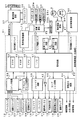
まず、遊技機の一例であるパチンコ遊技機の全体の構成について説明する。図1はパチンコ遊技機1を正面からみた正面図、図2はパチンコ遊技機1の内部構造を示す全体背面図、図3はパチンコ遊技機1の遊技盤を背面からみた背面図である。なお、ここでは、遊技機の一例としてパチンコ遊技機を示すが、本発明はパチンコ遊技機に限られず、例えばコイン遊技機等であってもよい。
【0024】
図1に示すように、パチンコ遊技機1は、額縁状に形成されたガラス扉枠2を有する。ガラス扉枠2の下部表面には打球供給皿3がある。打球供給皿3の下部には、打球供給皿3からあふれた景品玉を貯留する余剰玉受皿4と打球を発射する打球操作ハンドル(操作ノブ)5が設けられている。ガラス扉枠2の後方には、遊技盤6が着脱可能に取り付けられている。また、遊技盤6の前面には遊技領域7が設けられている。
【0025】
遊技領域7の中央付近には、複数種類の図柄を可変表示するための可変表示部9と7セグメントLEDによる可変表示器10とを含む可変表示装置8が設けられている。この実施の形態では、可変表示部9には、「左」、「中」、「右」の3つの図柄表示エリアがある。可変表示装置8の側部には、打球を導く通過ゲート11が設けられている。通過ゲート11を通過した打球は、玉出口13を経て始動入賞口14の方に導かれる。通過ゲート11と玉出口13との間の通路には、通過ゲート11を通過した打球を検出するゲートスイッチ12がある。また、始動入賞口14に入った入賞球は、遊技盤6の背面に導かれ、始動口スイッチ17によって検出される。また、始動入賞口14の下部には開閉動作を行う可変入賞球装置15が設けられている。可変入賞球装置15は、ソレノイド16によって開状態とされる。
【0026】
可変入賞球装置15の下部には、特定遊技状態(大当り状態)においてソレノイド21によって開状態とされる開閉板20が設けられている。この実施の形態では、開閉板20が大入賞口を開閉する手段となる。開閉板20から遊技盤6の背面に導かれた入賞球のうち一方(Vゾーン)に入った入賞球はVカウントスイッチ22で検出される。また、開閉板20からの入賞球はカウントスイッチ23で検出される。可変表示装置8の下部には、始動入賞口14に入った入賞球数を表示する4個の表示部を有する始動入賞記憶表示器18が設けられている。この例では、4個を上限として、始動入賞がある毎に、始動入賞記憶表示器18は点灯している表示部を1つずつ増やす。そして、可変表示部9の可変表示が開始される毎に、点灯している表示部を1つ減らす。
【0027】
遊技盤6には、複数の入賞口19,24が設けられている。遊技領域7の左右周辺には、遊技中に点滅表示される装飾ランプ25が設けられ、下部には、入賞しなかった打球を吸収するアウト口26がある。また、遊技領域7の外側の左右上部には、効果音を発する2つのスピーカ27が設けられている。遊技領域7の外周には、遊技効果LED28aおよび遊技効果ランプ28b,28cが設けられている。
【0028】
そして、この例では、一方のスピーカ27の近傍に、景品玉払出時に点灯する賞球ランプ51が設けられ、他方のスピーカ27の近傍に、補給玉が切れたときに点灯する球切れランプ52が設けられている。さらに、図1には、パチンコ遊技台1に隣接して設置され、プリペイドカードが挿入されることによって球貸しを可能にするカードユニット50も示されている。
【0029】
また、遊技盤6の前面には、報知用LED41が設けられている。報知用LED41は、遊技機1の遊技制御基板に搭載されている1チップマイクロコンピュータ等がバックアップ電源でバックアップされていることを遊技者等に報知するためのものである。
【0030】
カードユニット50には、使用可能状態であるか否かを示す使用可表示ランプ151、カード内に記録された残額情報に端数(100円未満の数)が存在する場合にその端数を打球供給皿3の近傍に設けられる度数表示LEDに表示させるための端数表示スイッチ152、カードユニット50がいずれの側のパチンコ遊技機1に対応しているのかを示す連結台方向表示器153、カードユニット50内にカードが投入されていることを示すカード投入表示ランプ154、記録媒体としてのカードが挿入されるカード挿入口155、およびカード挿入口155の裏面に設けられているカードリーダライタの機構を点検する場合にカードユニット50を解放するためのカードユニット錠156が設けられている。
【0031】
打球発射装置から発射された打球は、打球レールを通って遊技領域7に入り、その後、遊技領域7を下りてくる。打球が通過ゲート11を通ってゲートスイッチ12で検出されると、可変表示器10の表示数字が連続的に変化する状態になる。また、打球が始動入賞口14に入り始動口スイッチ17で検出されると、図柄の変動を開始できる状態であれば、可変表示部9内の図柄が回転を始める。図柄の変動を開始できる状態でなければ、始動入賞記憶を1増やす。
【0032】
可変表示部9内の画像の回転は、一定時間が経過したときに停止する。停止時の画像の組み合わせが大当り図柄の組み合わせであると、大当り遊技状態に移行する。すなわち、開閉板20が、一定時間経過するまで、または、所定個数(例えば10個)の打球が入賞するまで開放する。そして、開閉板20の開放中に打球が特定入賞領域に入賞しVカウントスイッチ22で検出されると、継続権が発生し開閉板20の開放が再度行われる。継続権の発生は、所定回数(例えば15ラウンド)許容される。
【0033】
停止時の可変表示部9内の画像の組み合わせが確率変動を伴う大当り図柄の組み合わせである場合には、次に大当りとなる確率が高くなる。すなわち、高確率状態という遊技者にとってさらに有利な状態となる。また、可変表示器10における停止図柄が所定の図柄(当り図柄)である場合に、可変入賞球装置15が所定時間だけ開状態になる。さらに、高確率状態では、可変表示器10における停止図柄が当り図柄になる確率が高められるとともに、可変入賞球装置15の開放時間と開放回数が高められる。
【0034】
次に、パチンコ遊技機1の裏面の構造について図2を参照して説明する。
可変表示装置8の背面では、図2に示すように、機構板36の上部に景品玉タンク38が設けられ、パチンコ遊技機1が遊技機設置島に設置された状態でその上方から景品玉が景品玉タンク38に供給される。景品玉タンク38内の景品玉は、誘導樋39を通って玉払出装置に至る。
【0035】
機構板36には、中継基板30を介して可変表示部9を制御する可変表示制御ユニット29、基板ケース32に覆われ遊技制御用マイクロコンピュータ等が搭載された遊技制御基板(主基板)31、可変表示制御ユニット29と遊技制御基板31との間の信号を中継するための中継基板33、および景品玉の払出制御を行う賞球制御用マイクロコンピュータ等が搭載された賞球制御基板37が設置されている。さらに、機構板36の下部には、モータの回転力を利用して打球を遊技領域7に発射する打球発射装置34と、遊技効果ランプ・LED28a,28b,28c、賞球ランプ51および球切れランプ52に信号を送るためのランプ制御基板35が設置されている。
【0036】
また、図3はパチンコ遊技機1の遊技盤を背面からみた背面図である。誘導樋39を通った玉は、図3に示されるように、球切れ検出器187a,187bを通過して玉供給樋186a,186bを経て玉払出装置97に至る。玉払出装置97から払い出された景品玉は、連絡口45を通ってパチンコ遊技機1の前面に設けられている打球供給皿3に供給される。連絡口45の側方には、パチンコ遊技機1の前面に設けられている余剰玉受皿4に連通する余剰玉通路46が形成されている。入賞にもとづく景品玉が多数払い出されて打球供給皿3が満杯になり、ついには景品玉が連絡口45に到達した後さらに景品玉が払い出されると景品玉は、余剰玉通路46を経て余剰玉受皿4に導かれる。さらに景品玉が払い出されると、感知レバー47が満タンスイッチ48を押圧して満タンスイッチ48がオンする。その状態では、玉払出装置97内のステッピングモータの回転が停止して玉払出装置97の動作が停止するとともに、必要に応じて打球発射装置34の駆動も停止する。
【0037】
賞球払出制御を行うために、入賞球検出スイッチ(図示せず)、始動口スイッチ17およびVカウントスイッチ22からの信号が、主基板31に送られる。入賞があったことは入賞球検出スイッチで検出される。主基板31に入賞球検出スイッチのオン信号が送られると、主基板31から賞球制御基板37に賞球制御コマンドが送られる。例えば、始動口スイッチ17のオンに対応して入賞球検出スイッチがオンすると、賞球個数「6」を示す賞球制御コマンドが出力され、カウントスイッチ23またはVカウントスイッチ22のオンに対応して入賞球検出スイッチがオンすると、賞球個数「15」を示す賞球制御コマンドが出力される。そして、それらのスイッチがオンしない場合に入賞球検出スイッチがオンすると、賞球個数「10」を示す賞球制御コマンドが出力される。
【0038】
図4は、主基板31における回路構成の一例を示すブロック図である。なお、図4には、賞球制御基板37、ランプ制御基板35、音声制御基板70、発射制御基板91および表示制御基板80も示されている。主基板31には、プログラムに従ってパチンコ遊技機1を制御する基本回路53と、ゲートスイッチ12、始動口スイッチ17、Vカウントスイッチ22、カウントスイッチ23および入賞球検出スイッチ99からの信号を基本回路53に与えるスイッチ回路58と、可変入賞球装置15を開閉するソレノイド16および開閉板20を開閉するソレノイド21を基本回路53からの指令に従って駆動するソレノイド回路59と、始動記憶表示器18の点灯および滅灯を行うとともに7セグメントLEDによる可変表示器10と装飾ランプ25とを駆動するランプ・LED回路60とを含む。
【0039】
さらに、バッファ回路42を介して報知用LED41が接続されている。報知用LED41は、CPU56が内蔵する出力ポートに接続される。また、報知用LED41は、バックアップ電源から給電される。
【0040】
また、基本回路53から与えられるデータに従って、大当りの発生を示す大当り情報、可変表示部9の画像表示開始に利用された始動入賞球の個数を示す有効始動情報、確率変動が生じたことを示す確変情報等をホール管理コンピュータ等のホストコンピュータに対して出力する情報出力回路64を含む。
【0041】
基本回路53は、ゲーム制御用のプログラム等を記憶するROM54、ワークメモリとして使用されるRAM55、制御用のプログラムに従って制御動作を行うCPU56およびI/Oポート部57を含む。この実施の形態では、ROM54,RAM55はCPU56に内蔵されている。すなわち、CPU56は、1チップマイクロコンピュータである。なお、1チップマイクロコンピュータは、少なくともRAM55が内蔵されていればよく、ROM54およびI/Oポート部57は外付けであってもよい。
【0042】
さらに、主基板31には、電源投入時に基本回路53をリセットするための初期リセット回路65と、定期的(例えば、2ms毎)に基本回路53にリセットパルスを与えてゲーム制御用のプログラムを先頭から再度実行させるための定期リセット回路66と、基本回路53から与えられるアドレス信号をデコードしてI/Oポート部57のうちのいずれかのI/Oポートを選択するための信号を出力するアドレスデコード回路67とが設けられている。
なお、玉払出装置97から主基板31に入力されるスイッチ情報もあるが、図4ではそれらは省略されている。
【0043】
遊技球を打撃して発射する打球発射装置は発射制御基板91上の回路によって制御される駆動モータ94で駆動される。そして、駆動モータ94の駆動力は、操作ノブ5の操作量に従って調整される。すなわち、発射制御基板91上の回路によって、操作ノブ5の操作量に応じた速度で打球が発射されるように制御される。
【0044】
図5は、表示制御基板80内の回路構成を、可変表示部9の一実現例であるCRT82および主基板31の出力ポート(ポートA,B)571,572および出力バッファ回路63とともに示すブロック図である。出力ポート571からは8ビットのデータが出力され、出力ポート572からは1ビットのストローブ信号(INT信号)が出力される。
【0045】
表示制御用CPU101は、制御データROM102に格納されたプログラムに従って動作し、主基板31からノイズフィルタ107および入力バッファ回路105を介してストローブ信号が入力されると、入力バッファ回路105を介して表示制御コマンドを受信する。入力バッファ回路105として、例えば汎用ICである74HC244を使用することができる。なお、表示制御用CPU101がI/Oポートを内蔵していない場合には、入力バッファ回路105と表示制御用CPU101との間に、I/Oポートが設けられる。
【0046】
そして、表示制御用CPU101は、受信した表示制御コマンドに従って、CRT82に表示される画面の表示制御を行う。具体的には、表示制御コマンドに応じた指令をVDP103に与える。VDP103は、キャラクタROM86から必要なデータを読み出す。VDP103は、入力したデータに従ってCRT82に表示するための画像データを生成し、その画像データをVRAM87に格納する。そして、VRAM87内の画像データは、R,G,B信号に変換され、D−A変換回路104でアナログ信号に変換されてCRT82に出力される。
【0047】
なお、図5には、VDP103をリセットするためのリセット回路83、VDP103に動作クロックを与えるための発振回路85、および使用頻度の高い画像データを格納するキャラクタROM86も示されている。キャラクタROM86に格納される使用頻度の高い画像データとは、例えば、CRT82に表示される人物、動物、または、文字、図形もしくは記号等からなる画像などである。この実施の形態では、表示制御用CPU101は、1チップマイクロコンピュータであり、少なくともRAMが内蔵されている。
【0048】
入力バッファ回路105は、主基板31から表示制御基板80へ向かう方向にのみ信号を通過させることができる。従って、表示制御基板80側から主基板31側に信号が伝わる余地はない。表示制御基板80内の回路に不正改造が加えられても、不正改造によって出力される信号が主基板31側に伝わることはない。なお、出力ポート571,572の出力をそのまま表示制御基板80に出力してもよいが、単方向にのみ信号伝達可能な出力バッファ回路63を設けることによって、主基板31から表示制御基板80への一方向性の信号伝達をより確実にすることができる。また、高周波信号を遮断するノイズフィルタ107として、例えば3端子コンデンサやフェライトビーズが使用されるが、ノイズフィルタ107の存在によって、表示制御コマンドに基板間でノイズが乗ったとしても、その影響は除去される。
【0049】
図6は、主基板31における音声制御コマンドの信号送信部分および音声制御基板70の構成例を示すブロック図である。この実施の形態では、遊技進行に応じて、遊技領域7の外側に設けられているスピーカ27の音声出力を指示するための音声制御コマンドが、主基板31から音声制御基板70に出力される。
【0050】
図6に示すように、音声制御コマンドは、基本回路53におけるI/Oポート部57の出力ポート(出力ポートC,D)573,574から出力される。出力ポート573からは8ビットのデータが出力され、出力ポート574からは1ビットのストローブ信号(INT信号)が出力される。音声制御基板70において、主基板31からの各信号は、入力バッファ回路705を介して音声制御用CPU701に入力する。なお、音声制御用CPU701がI/Oポートを内蔵していない場合には、入力バッファ回路705と音声制御用CPU701との間に、I/Oポートが設けられる。また、この実施の形態では、音声制御用CPU701は、1チップマイクロコンピュータであり、少なくともRAMが内蔵されている。
【0051】
そして、例えばディジタルシグナルプロセッサによる音声合成回路702は、音声制御用CPU701の指示に応じた音声や効果音を発生し音量切替回路703に出力する。音量切替回路703は、音声制御用CPU701の出力レベルを、設定されている音量に応じたレベルにして音量増幅回路704に出力する。音量増幅回路704は、増幅した音声信号をスピーカ27に出力する。
【0052】
入力バッファ回路705として、例えば、汎用のCMOS−ICである74HC244が用いられる。74HC244のイネーブル端子には、常にローレベル(GNDレベル)が与えられている。よって、各バッファの出力レベルは、入力レベルすなわち主基板31からの信号レベルに確定している。よって、音声制御基板70側から主基板31側に信号が伝わる余地はない。従って、音声制御基板70内の回路に不正改造が加えられても、不正改造によって出力される信号が主基板31側に伝わることはない。なお、入力バッファ回路705の入力側にノイズフィルタを設けてもよい。
【0053】
また、主基板31において、出力ポート574,575の外側にバッファ回路67が設けられている。バッファ回路67として、例えば、汎用のCMOS−ICである74HC244が用いられる。イネーブル端子には常にローレベル(GNDレベル)が与えられている。このような構成によれば、外部から主基板31の内部に入力される信号が阻止されるので、音声制御基板70から主基板31に信号が与えられる可能性がある信号ラインをさらに確実になくすことができる。
【0054】
図7は、主基板31およびランプ制御基板35における信号送受信部分を示すブロック図である。この実施の形態では、遊技領域7の外側に設けられている遊技効果LED28aおよび遊技効果ランプ28b,28cの点灯/消灯と、賞球ランプ51および球切れランプ52の点灯/消灯を示すランプ制御コマンドが出力される。
【0055】
図7に示すように、ランプ制御に関するランプ制御コマンドは、基本回路53におけるI/Oポート部57の出力ポート(出力ポートE,F)575,576から出力される。出力ポート575は8ビットのデータを出力し、出力ポート576は1ビットのストローブ信号(INT信号)を出力する。ランプ制御基板35において、主基板31からの制御コマンドは、入力バッファ回路355を介してランプ制御用CPU351に入力する。なお、ランプ制御用CPU351がI/Oポートを内蔵していない場合には、入力バッファ回路355とランプ制御用CPU351との間に、I/Oポートが設けられる。また、この実施の形態では、ランプ制御用CPU351は、1チップマイクロコンピュータであり、少なくともRAMが内蔵されている。
【0056】
ランプ制御基板35において、ランプ制御用CPU351は、各制御コマンドに応じて定義されている遊技効果LED28aおよび遊技効果ランプ28b,28cの点灯/消灯パターンに従って、遊技効果LED28aおよび遊技効果ランプ28b,28cに対して点灯/消灯信号を出力する。点灯/消灯信号は、遊技効果LED28aおよび遊技効果ランプ28b,28cに出力される。なお、点灯/消灯パターンは、ランプ制御用CPU351の内蔵ROMまたは外付けROMに記憶されている。
【0057】
主基板31において、CPU56は、賞球時に賞球ランプ点灯を指示する制御コマンドを出力し、遊技盤裏面の遊技球補給路に設置されている球切れ検出センサがオンすると球切れランプ点灯を指示する制御コマンドを出力する。ランプ制御基板35において、各制御コマンドは、入力バッファ回路355を介してランプ制御用CPU351に入力する。ランプ制御用CPU351は、それらの制御コマンドに応じて、賞球ランプ51および球切れランプ52を点灯/消灯する。
【0058】
入力バッファ回路355として、例えば、汎用のCMOS−ICである74HC244が用いられる。74HC244のイネーブル端子には、常にローレベル(GNDレベル)が与えられている。よって、各バッファの出力レベルは、入力レベルすなわち主基板31からの信号レベルに確定している。従って、ランプ制御基板35側から主基板31側に信号が伝わる余地はない。たとえ、ランプ制御基板35内の回路に不正改造が加えられても、不正改造によって出力される信号がメイン基板31側に伝わることはない。なお、入力バッファ回路355の入力側にノイズフィルタを設けてもよい。
【0059】
図7に示された構成では、ランプ制御基板35から主基板31に信号が与えらる可能性がある信号ラインをなくすことができる。すなわち、主基板31からランプ制御基板35への信号の一方向性が確実になり、主基板31における遊技制御に対してランプ制御基板35が影響を及ぼす可能性がなくなる。この結果、例えば、ランプ制御基板35において、主基板31の基本回路53に大当りを生じさせるための不正信号を与えるような改造を行ったとしても、不正信号を主基板31に伝えることはできない。
【0060】
さらに、主基板31において、出力ポート575,576の外側にバッファ回路62が設けられている。バッファ回路62として、例えば、汎用のCMOS−ICである74HC244が用いられる。イネーブル端子には常にローレベル(GNDレベル)が与えられている。このような構成によれば、外部から主基板31の内部に入力される信号が阻止されるので、ランプ制御基板35から主基板31に信号が与えらる可能性がある信号ラインをより確実になくすことができる。
【0061】
なお、図7では、ランプ制御用CPU351の内蔵出力ポートから遊技効果LED28a、遊技効果ランプ28b,28c、賞球ランプ51および球切れランプ52に点灯または消灯を指示する信号が出力されているが、実際には、出力ポートと各ランプ・LEDとの間にドライバ回路が挿入されている。
【0062】
図8は、賞球制御基板37および玉払出装置97の構成要素などの賞球に関連する構成要素を示すブロック図である。図8に示すように、入賞球検出スイッチ99および満タンスイッチ48からの検出信号は、中継基板71を介して主基板31のI/Oポート57に入力される。入賞球排出ソレノイド127は、遊技盤裏面の入賞球流下路の途中に設けられている玉止め部材を駆動するものであって、玉止め部材に入賞球が停止している状態で入賞球検出スイッチ99によって入賞球が検出される。また、満タンスイッチ48は、余剰玉受皿4の満タンを検出するスイッチである。
【0063】
球切れ検出スイッチ167および球切れスイッチ187(187a,187b)からの検出信号は、中継基板72および中継基板71を介して主基板31のI/Oポート57に入力される。球切れ検出スイッチ167は景品玉タンク38内の補給玉の不足を検出するスイッチであり、球切れスイッチ187は、景品玉通路内の景品玉の有無を検出するスイッチである。
【0064】
主基板31のCPU56は、球切れ検出スイッチ167または球切れスイッチ187からの検出信号が球切れ状態を示しているか、または、満タンスイッチ48からの検出信号が満タン状態を示していると、球貸し禁止を指示する賞球制御コマンドを送出する。球貸し禁止を指示する賞球制御コマンドを受信すると、賞球制御基板37の賞球制御用CPU371は、球貸し処理を停止する。
【0065】
さらに、賞球カウントスイッチ301Aからの検出信号も、中継基板72および中継基板71を介して主基板31のI/Oポート57に入力される。また、主基板31のI/Oポート57から入賞球排出ソレノイド127への駆動信号は、中継基板71を介して入賞球排出ソレノイド127に供給される。なお、賞球カウントスイッチ301Aは、玉払出装置97の賞球機構部分に設けられ、実際に払い出された賞球を検出する。
【0066】
入賞があると、賞球制御基板37には、主基板31の出力ポート(ポートG,H)577,578から賞球個数を示す賞球制御コマンドが入力される。出力ポート577は8ビットのデータを出力し、出力ポート578は1ビットのストローブ信号(INT信号)を出力する。賞球個数を示す賞球制御コマンドは、入力バッファ回路373を介してI/Oポート372aに入力される。賞球制御用CPU371は、I/Oポート372aを介して賞球制御コマンドを入力し、賞球制御コマンドに応じて玉払出装置97を駆動して賞球払出を行う。なお、この実施の形態では、賞球制御用CPU371は、1チップマイクロコンピュータであり、少なくともRAMが内蔵されている。
【0067】
入力バッファ回路373における各バッファは、主基板31から賞球制御基板37へ向かう方向にのみ信号を通過させることができる。従って、賞球制御基板37側から主基板31側に信号が伝わる余地はない。賞球制御基板37内の回路に不正改造が加えられても、不正改造によって出力される信号が主基板31側に伝わることはない。なお、入力バッファ回路373の入力側にノイズフィルタを設けてもよい。
【0068】
また、主基板31において、賞球制御コマンドを出力する出力ポート577,578の外側にバッファ回路68が設けられている。このような構成によれば、外部から主基板31の内部に入力される信号が阻止されるので、賞球制御基板37から主基板31に信号が与えらる可能性がある信号ラインをより確実になくすことができる。
【0069】
また、賞球制御用CPU371は、出力ポート372gを介して、貸し玉数を示す球貸し個数信号をターミナル基板160に出力し、ブザー駆動信号をブザー基板75に出力する。ブザー基板75にはブザーが搭載されている。さらに、出力ポート372eを介して、エラー表示用LED374にエラー信号を出力する。
【0070】
さらに、賞球制御基板37の入力ポート372bには、中継基板72を介して、賞球カウントスイッチ301Aの検出信号および球貸しカウントスイッチ301Bの検出信号が入力される。球貸しカウントスイッチ301Bは、実際に貸し出された遊技球を検出する。賞球制御基板37からの払出モータ289への駆動信号は、出力ポート372cおよび中継基板72を介して玉払出装置97の賞球機構部分における払出モータ289に伝えられる。
【0071】
カードユニット50には、カードユニット制御用マイクロコンピュータが搭載されている。また、カードユニット50には、端数表示スイッチ152、連結台方向表示器153、カード投入表示ランプ154およびカード挿入口155が設けられている(図1参照)。残高表示基板74には、打球供給皿3の近傍に設けられている度数表示LED、球貸しスイッチおよび返却スイッチが接続される。
【0072】
残高表示基板74からカードユニット50には、遊技者の操作に応じて、球貸しスイッチ信号および返却スイッチ信号が賞球制御基板37を介して与えられる。また、カードユニット50から残高表示基板74には、プリペイドカードの残高を示すカード残高表示信号および球貸し可表示信号が賞球制御基板37を介して与えられる。カードユニット50と賞球制御基板37の間では、ユニット操作信号(BRDY信号)、球貸し要求信号(BRQ信号)、球貸し完了信号(EXS信号)およびパチンコ機動作信号(PRDY信号)がI/Oポート372fを介してやりとりされる。
【0073】
パチンコ遊技機1の電源が投入されると、賞球制御基板37の賞球制御用CPU371は、カードユニット50にPRDY信号を出力する。カードユニット50においてカードが受け付けられ、球貸しスイッチが操作され球貸しスイッチ信号が入力されると、カードユニット制御用マイクロコンピュータは、賞球制御基板37にBRDY信号を出力する。この時点から所定の遅延時間が経過すると、カードユニット制御用マイクロコンピュータは、賞球制御基板37にBRQ信号を出力する。そして、賞球制御基板37の賞球制御用CPU371は、払出モータ289を駆動し、所定個の貸し玉を遊技者に払い出す。そして、払出が完了したら、賞球制御用CPU371は、カードユニット50にEXS信号を出力する。
【0074】
以上のように、カードユニット50からの信号は全て賞球制御基板37に入力される構成になっている。従って、球貸し制御に関して、カードユニット50から主基板31に信号が入力されることはなく、主基板31の基本回路53にカードユニット50の側から不正に信号が入力される余地はない。なお、主基板31および賞球制御基板37には、ソレノイドおよびモータやランプを駆動するためのドライバ回路が搭載されているが、図8では、それらの回路は省略されている。
【0075】
この実施の形態では、上述した主基板31のCPU56、表示制御用CPU101、音声制御用CPU701、ランプ制御用CPU351および賞球制御用CPU371は、バックアップ電源でバックアップされている。すなわち、遊技機に対する電力供給が停止しても、それらのCPUは、所定期間は動作可能になっている。また、上述したように、主基板31のCPU56、表示制御用CPU101、音声制御用CPU701、ランプ制御用CPU351および賞球制御用CPU371は、CPU部の他に少なくともRAMを内蔵しているので、遊技機に対する電力供給が停止しても、バックアップ電源によって内蔵RAMは記憶内容を保持することができる。そして、各CPUは、電源電圧の低下を検出すると、所定の処理を行った後に電源復旧待ちの状態になる。
【0076】
図9は、電源監視および電源バックアップのためのCPU周りの一構成例を示すブロック図である。図9に示すように、電源監視用IC902は、12V電圧を導入し、12V電圧を監視することによって電源断の発生を検出する。具体的には、12V電圧が所定値(例えば12Vの80%)以下になったら、電源断が生ずるとして、CPU901に割り込み信号を与える。CPU901において、この割り込みは、外部割込(INT)端子に入力されている。また、INT端子に入力される信号は、CPU901が内蔵する入力ポートにも入力されている。従って、CPU901は、割込処理において、入力ポートのレベルを確認することによって電源断の発生を検出することができる。なお、入力ポートに割り込み信号を供給せずに、割込端子にのみ電源監視用IC902からの信号を接続する構成でもよい。
【0077】
また、図9に示すように、報知用LED41は、バックアップ電源から給電がなされている。
【0078】
電源監視用IC902が電源断を検知するための所定値は、通常時の電圧より低いが、賞球制御用CPU371が暫くの間動作しうる程度の電圧である。また、電源監視用IC902が、CPU901が必要とする電圧(この例では+5V)よりも高い電圧を監視するように構成されているので、CPU901が必要とする電圧に対して監視範囲を広げることができる。従って、より精密な監視を行うことができる。さらに、監視電圧として+12Vを用いる場合には、遊技機の各種スイッチに供給される電圧が+12Vであることから、電源瞬断時のスイッチオン誤検出の防止も期待できる。すなわち、+12V電源の電圧が低下するとスイッチ出力がオン状態を呈するようになるが、同じ+12V電源電圧を監視して電源断を認識すれば、スイッチ出力がオン状態を呈する前に電源復旧待ちの状態に入ってスイッチ出力を検出しない状態となることができる。
【0079】
+5V電源から電力が供給されていない間、CPU901は、電源基板から供給されるバックアップ電源によって動作する。そして、+5V電源が復旧すると、初期リセット回路905からリセット信号が発せられるので、CPU901は、通常の動作状態に復帰する。なお、初期リセット回路905は、図4に示された初期リセット回路65と同様の構成である。すなわち、電源電位が0Vから立ち上がって所定レベルになると、CPU901に与えられる初期リセット信号を例えばハイレベルに変化させる。
【0080】
ここでは、初期リセット回路905からリセット信号によって通常の動作状態に復帰するとしたが、CPU901の入力ポートに電源監視用IC902からの割込信号が導入されている場合には、その信号レベルが電源断時のレベルを示さなくなったことを検知して電源が復旧したことを検出し、通常の動作状態に復帰するようにしてもよい。
【0081】
図9に示すような構成は、各遊技用装置制御基板(この実施の形態では主基板31、表示制御基板80、音声制御基板70、ランプ制御基板35および賞球制御基板37)に適用される。すなわち、各基板に電源監視用IC902が搭載される。また、CPU901周りの構成は、主基板31のCPU56、表示制御用CPU101、音声制御用CPU701、ランプ制御用CPU351および賞球制御用CPU371に適用される。
【0082】
図10は、電源基板910の一構成例を示すブロック図である。電源基板910は、主基板31、表示制御基板80、音声制御基板70、ランプ制御基板35および賞球制御基板37等の制御基板と独立して設置され、遊技機内の各制御基板および機構部品が使用する電圧を生成する。この例では、AC24V、DC+30V、DC+21V、DC+12VおよびDC+5Vを生成する。また、バックアップ電源となるコンデンサ916は、DC+5Vすなわち各基板上のIC等を駆動する電源のラインから充電される。
【0083】
トランス911は、交流電源からの交流電圧を24Vに変換する。AC24V電圧は、コネクタ915に出力される。また、整流回路912は、AC24Vから所定電圧の直流電圧を生成し、DC−DCコンバータ913に供給する。DC−DCコンバータ913は、+30V、+21V、+12Vおよび+5Vを生成してコネクタ915に出力する。コネクタ915は例えば中継基板に接続され、中継基板から各制御基板および機構部品に必要な電圧の電力が供給される。
【0084】
DC−DCコンバータ913からの+5Vラインは分岐してバックアップ+5Vラインを形成する。バックアップ+5Vラインとグラウンドレベルとの間には大容量のコンデンサ916が接続されている。コンデンサ916は、遊技機に対する電力供給が遮断されたときの各CPUに対するバックアップ電源となる。
【0085】
なお、バックアップ電源として、+5V電源から充電可能な電池を用いてもよい。電池を用いる場合には、+5V電源から電力供給されない状態が所定時間継続すると容量がなくなるような充電池が用いられる。
【0086】
図11は、他の構成の電源基板910を制御基板920とともに示すブロック図である。制御基板920は、主基板31、表示制御基板80、音声制御基板70、ランプ制御基板35および賞球制御基板37等に相当するものである。この例では、電源基板910では、AC24V、DC+30V、DC+21V、DC+12VおよびDC+8Vが生成される。
【0087】
そして、制御基板920には、電源基板910から供給される+8Vを+5Vに変換する8V−5V変換回路921が設けられている。制御基板920上の+5Vで動作する制御回路922には8V−5V変換回路921から電圧供給される。8V−5V変換回路921は、例えばスイッチングレギュレータ等を含むDC−DCコンバータで構成される。なお、制御回路922は、制御基板920上の各回路であるが、図11では、CPUに相当するものが図示されている。
【0088】
図11に示す電源回路910において、バックアップ電源用のコンデンサ916が設置されている。この例では、コンデンサ916は、制御基板920上の8V−5V変換回路921が生成した+5V電圧によって充電される。遊技機に対する電力供給が遮断されたときに、各CPUに対してコンデンサ916から電源供給されることは図10に示された構成の場合と同様である。また、コンデンサ916に代えて電池を用いてもよいことも同様である。
【0089】
各制御基板において使用される+5V電圧を電源基板910でまとめて生成する場合には、電源基板910から各制御基板に配線される電源ラインにノイズがのる可能性があるが、図11に示されたように、+5Vよりも高い電圧を各制御基板に供給し、各制御基板において、その電圧から+5Vを生成するように構成すれば、基板間の電源ラインにのったノイズをキャンセルすることができる。
【0090】
次に遊技機の動作について説明する。
図12は、主基板31におけるCPU56の動作を示すフローチャートである。上述したように、この処理は、定期リセット回路66が発するリセットパルスによって、例えば2ms毎に起動される。CPU56が起動されると、CPU56は、まず、クロックモニタ制御を動作可能状態にするために、内蔵されているクロックモニタレジスタをクロックモニタイネーブル状態に設定する(ステップS1)。なお、クロックモニタ制御とは、入力されるクロック信号の低下または停止を検出すると、CPU56の内部で自動的にリセットを発生する制御である。
【0091】
次いで、CPU56は、スタックポインタの指定アドレスをセットするためのスタックセット処理を行う(ステップS2)。この例では、スタックポインタに00FFHが設定される。そして、システムチェック処理を行う(ステップS3)。システムチェック処理では、CPU56は、RAM55にエラーが含まれているか判定し、エラーが含まれている場合には、RAM55を初期化するなどの処理を行う。さらに、電源投入時であれば、バックアップRAM領域にセーブされているレジスタ内容を復元する制御も行う。
【0092】
次に、表示制御基板80に送出される表示制御コマンドをRAM55の所定の領域に設定する処理を行った後に(表示制御データ設定処理:ステップS4)、表示制御コマンドを出力する処理を行う(表示制御データ出力処理:ステップS5)。
【0093】
次いで、各種出力データの格納領域の内容を各出力ポートに出力する処理を行う(データ出力処理:ステップS6)。また、ホール管理用コンピュータに出力される大当り情報、始動情報、確率変動情報などの出力データを格納領域に設定する出力データ設定処理を行う(ステップS8)。さらに、パチンコ遊技機1の内部に備えられている自己診断機能によって種々の異常診断処理が行われ、その結果に応じて必要ならば警報が発せられる(エラー処理:ステップS9)。
【0094】
次に、遊技制御に用いられる大当り判定用の乱数等の各判定用乱数を示す各カウンタを更新する処理を行う(ステップS10)。
【0095】
次に、CPU56は、特別図柄プロセス処理を行う(ステップS11)。特別図柄プロセス制御では、遊技状態に応じてパチンコ遊技機1を所定の順序で制御するための特別図柄プロセスフラグに従って該当する処理が選び出されて実行される。そして、特別図柄プロセスフラグの値は、遊技状態に応じて各処理中に更新される。また、普通図柄プロセス処理を行う(ステップS12)。普通図柄プロセス処理では、7セグメントLEDによる可変表示器10を所定の順序で制御するための普通図柄プロセスフラグに従って該当する処理が選び出されて実行される。そして、普通図柄プロセスフラグの値は、遊技状態に応じて各処理中に更新される。
【0096】
さらに、CPU56は、スイッチ回路58を介して、ゲートセンサ12、始動口センサ17およびカウントセンサ23の状態を入力し、各入賞口や入賞装置に対する入賞があったか否か判定する(スイッチ処理:ステップS13)。
【0097】
CPU56は、さらに、停止図柄の種類を決定する乱数等の表示用乱数を更新する処理を行う(ステップS15)。
【0098】
また、CPU56は、賞球制御基板37との間の信号処理を行う(ステップS16)。すなわち、所定の条件が成立すると賞球制御基板37に賞球制御コマンドを出力する。賞球制御基板37に搭載されている賞球制御用CPUは、賞球制御コマンドに応じて玉払出装置97を駆動する。その後、CPU56は、次に定期リセット回路66からリセットパルスが与えられるまで、ステップS17の表示用乱数更新処理を繰り返す。
【0099】
図13は、CPU56の割込処理を示すフローチャートである。上述したように、電源監視用IC902が電源電圧の低下を検出すると、CPU56に割込がかかる。なお、割込端子に他の割込要因も入力されるような場合や電源電圧低下の検出をより確実にしたいような場合には、図9に示されているように入力ポートに電源監視用IC902の出力を導入し、割込処理において入力ポートのレベルを確認して電源電圧の低下による割込が発生したことを検知してもよい。
【0100】
電源電圧の低下にもとづく割込処理では、まず、CPU56は、割込禁止状態に設定する(ステップS20)。よって、以後、割込がかかることはない。従って、電源電圧低下中にCPU56に複数回の割込がかかることはない。
【0101】
そして、CPU56は、電源断時処理として、各レジスタの内容をバックアップRAM領域に格納する(ステップS21)。また、バックアップRAM領域のバックアップチェックデータ領域に適当な初期値を設定し(ステップS22)、初期値およびバックアップRAM領域に退避させた全データについて順次排他的論理和をとって(ステップS23)、最終的な演算値をバックアップパリティデータ領域に設定する(ステップS24)。
【0102】
さらに、CPU56は、報知用LED41を点灯して電源バックアップ中であることを遊技者や遊技店員に報知する(ステップS25)。遊技機に対する電力供給が停止した場合には、遊技制御は中断されるが、報知手段を設けることによって、遊技者や遊技店員は、容易にそのことを認識できる。また、遊技状態が保存されている状態であることが容易に認識できる。なお、ここでは、報知手段として専用の報知用LED41を例示したが、ブザーや他の発光体を用いてもよい。
【0103】
そして、CPU56は、RAMアクセスを禁止状態にして(ステップS26)、以後、遊技制御を停止する。停止状態は、遊技機への電力供給が再開されるまで継続する。
【0104】
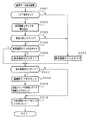
図14は、図12に示されたメイン処理におけるシステムチェック処理(ステップS3)の処理の一例を示すフローチャートである。遊技機への電力供給が再開されると、初期リセット回路65からCPU56に初期リセット信号が入力される。CPU56は、初期リセット信号に応じてメイン処理を開始するのであるが、システムチェック処理において、まず、電源投入時か否か確認する(ステップS41)。なお、CPU56から見ると、不測の電源断後に遊技機への電力供給が再開されたときも電源投入時である。
【0105】
電源投入時であれば、RAMアクセス許可状態とする(ステップS42)。そして、バックアップRAM領域のデータチェック(この例ではパリティチェック)を行う(ステップS43)。不測の電源断が生じた後に復旧した場合には、バックアップRAM領域のデータは保存されていたはずであるから、チェック結果は正常になる。チェック結果が正常にならないのは、一般に、遊技店における営業開始時の電源投入時である。そこで、チェック結果が正常でなければ(ステップS44)、レジスタおよびRAM領域をクリアする(ステップS45)。また、必要な初期設定を行う。
【0106】
チェック結果が正常であれば(ステップS44)、レジスタクリアのみを行う(ステップS46)。また、必要ならばバックアップRAM領域以外の領域(電源断して復旧時に保存されているいる必要のない領域)のクリア処理も行う。なお、レジスタクリア等を行うのは、一旦、初期状態(遊技店における営業開始時の電源投入時の状態)に戻すためであり、後述するように、一定時間後に、レジスタ状態は、不測の電源断時の状態に戻される。
【0107】
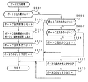
そして、CPU56は、表示制御基板80、音声制御基板70およびランプ制御基板35に初期状態復帰要求コマンドを送出する制御を行い(ステップS47)、遊技状態復帰用タイマをスタートさせる(ステップS48)。なお、ステップS47では、CPU56は、所定のRAM領域にコマンドをセットするとともに、コマンド送出要求フラグをセットする。表示制御基板80での表示制御コマンドに対するコマンド送出要求は、メイン処理における表示制御データ設定処理(ステップS4)で受け付けられ、その他の制御基板に対するコマンド送出要求は、メイン処理における例えばデータ出力処理(ステップS6)で受け付けられる。
【0108】
ステップS41において電源投入時でないことが確認されると、CPU56は、遊技状態復帰用タイマが動作中であるか否か確認する(ステップS50)。動作中であればタイムアウトしたか否かを確認する(ステップS51)。タイムアウトしていれば、表示制御基板80、音声制御基板70およびランプ制御基板35に遊技状態復帰要求コマンドを送出する制御を行うとともに(ステップS53)、バックアップRAM領域に保存されていたレジスタの内容を本来のレジスタに復帰させる(ステップS54)。
【0109】
図15は、バックアップパリティデータ作成方法を説明するための説明図である。ただし、図15に示す例では、簡単のために、バックアップデータRAM領域に退避されるデータのサイズを3バイトとする。電源電圧低下による割込処理において、図15の左側に示すように、バックアップチェックデータ領域に、初期データ(この例では00H)が設定される。次に、「00H」と「F0H」の排他的論理和がとられ、その結果と「16H」の排他的論理和がとられる。さらに、その結果と「DFH」の排他的論理和がとられる。そして、その結果(この例では「39H」)がバックアップパリティデータ領域に設定される。
【0110】
電源が再投入されたときには、図14に示されたステップS43でパリティ診断が行われるが、図15の右側はパリティ診断の例を示す説明図である。バックアップ領域の全データがそのまま保存されていれば、電源再投入時に、図15の左側に示すようなデータがバックアップ領域に設定されている。
【0111】
ステップS813の処理において、CPU56は、バックアップRAM領域のバックアップパリティデータ領域に設定されていたデータ(この例では「39H」)を初期データとして、バックアップデータ領域の各データについて順次排他的論理和をとる処理を行う。バックアップ領域の全データがそのまま保存されていれば、最終的な演算結果は、「00H」、すなわちバックアップチェックデータ領域に設定されているデータと一致する。バックアップRAM領域内のデータにビット誤りが生じていた場合には、最終的な演算結果は「00H」にならない。
【0112】
よって、CPU56は、最終的な演算結果とバックアップチェックデータ領域に設定されているデータとを比較して、一致すればパリティ診断正常とする。一致しなければ、パリティ診断異常とする。
【0113】
以上のように、この実施の形態では、遊技機に対する電力供給が停止すると、CPU56は、割込処理によってそのことを認識し、必要なデータをバックアップRAM領域に保存する処理を行う。その際、チェックデータもバックアップRAM領域に設定する。よって、CPU56は、不測の電源断からの復旧時に、データが正しく保存されていたか否かを確認することができる。また、割込処理において、割込禁止状態に設定するとともに、RAMアクセス禁止状態に設定する。よって、電源断が生じたときに、複数回の割込が生ずることはないし、また、電源電圧が低下していくときにCPU56のバスラインの状態が不定になるが、それによってRAM内容が破壊されることもない。なお、遊技機において使用されるCPUは、一般にRAMアクセス禁止機能を有している。
【0114】
また、後述するように、主基板31以外の各制御基板におけるCPUは、主基板31からの初期状態復帰コマンドに応じて、一旦、初期状態(遊技店における営業開始時の電源投入時の状態)に戻り、遊技状態復帰コマンドに応じて、不測の電源断が生じたときの状態に戻る。その間の時間は、遊技状態復帰用タイマ値によって決められる。このように、一旦初期状態に戻り、その後に、電源断時の遊技状態に戻るようにすれば、例えば可変表示部9に初期状態画面が表示された後に、元の遊技状態画面に復帰する。よって、遊技者は、遊技が再開されたことを容易に認識することができる。
【0115】
なお、この実施の形態では、初期リセット信号によってCPU56の動作状態が再開され、それまでCPU56は通常の遊技制御を行わない状態になるが、電源バックアップ中に、CPU56が、入力ポート(電源監視用IC902からの信号が入力されるポート)の状態を監視して電源復旧したことを確認するようにしてもよい。
【0116】
図16は、ROM55に設定されるテーブルの一構成例を示す説明図である。図16に示すように、ROM55には、例えば復帰用データテーブルと初期状態データテーブルとが設けられる。復帰用データテーブルには、例えば、表示制御基板80、音声制御基板70およびランプ制御基板35のそれぞれに送出する初期状態復帰コマンド、遊技状態復帰用タイマ値、ならびに表示制御基板80、音声制御基板70およびランプ制御基板35のそれぞれに送出する遊技状態復帰コマンド等の電源復旧時に必要となるパラメータが設定されている。従って、プログラムにおいてそれらのパラメータを設定する処理(ステップS47,S48,S53)では、復帰用データテーブルから必要なデータを読み出してパラメータ設定処理を行う。
【0117】
以上のように、復帰用データテーブルには、電源復旧時に複数の遊技用装置制御手段(遊技用装置を制御する手段)のそれぞれに送出するコマンドが認識可能に記憶されている。主基板31のCPU56すなわち遊技制御手段は、電源復旧時に復帰用データテーブルから送出すべきコマンドを認識し、認識したコマンドを各制御手段が搭載された基板に送出する。なお、復帰用データテーブルには、全ての遊技用制御手段に対するコマンドが設定されていてもよいし、1つ以上の必要な遊技用制御手段に対するコマンドが設定されていてもよい。
【0118】
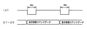
図17は、表示制御コマンドの構成例を示す説明図である。図17に示すように、表示制御コマンドは、8ビットのデータと、1ビットのストローブ信号(INT信号)とから構成されている。
【0119】
図18は、8ビットのデータによる表示制御コマンドデータの構成例を示す説明図である。図18に示すように、例えば、8ビットのうちの上位4ビットで制御の種類を指示し、下位4ビットで具体的制御内容を指示する。例えば、この例では、上位4ビットが[0,0,0,1]であれば、下位4ビットの数値でリーチ種類や全図柄停止等が指示される。また、上位4ビットが[1,0,0,0],[1,0,0,1]または[1,0,1,0]であれば、下位4ビットの数値で可変表示部9に可変表示される左図柄、中図柄または右図柄の停止図柄が指示される。
【0120】
また、上位4ビットが[1,1,1,0]であれば初期状態復帰コマンドであることを示す。上位4ビットが[1,1,1,1]であれば遊技状態復帰コマンドであることを示す。なお、それらのコマンドにおいて下位4ビットは例えば0に設定される。
【0121】
図19はCPU56が実行する特別図柄プロセス処理のプログラムの一例を示すフローチャートである。図19に示す特別図柄プロセス処理は、図12のフローチャートにおけるステップS11の具体的な処理である。CPU56は、特別図柄プロセス処理を行う際に、特別図柄プロセスフラグの値に応じて、図19に示すステップS300〜S309のうちのいずれかの処理を行う。各処理において、以下のような処理が実行される。
【0122】
特別図柄変動待ち処理(ステップS300):始動入賞口14(この実施の形態では可変入賞球装置15の入賞口)に打球入賞して始動口センサ17がオンするのを待つ。始動口センサ17がオンすると、始動入賞記憶数が満タンでなければ、始動入賞記憶数を+1するとともに大当り判定用乱数を抽出する。
【0123】
特別図柄判定処理(ステップS301):特別図柄の可変表示が開始できる状態になると、始動入賞記憶数を確認する。始動入賞記憶数が0でなければ、抽出されている大当り判定用乱数の値に応じて大当りとするかはずれとするか決定する。
停止図柄設定処理(ステップS302):左右中図柄の停止図柄を決定する。
【0124】
リーチ動作設定処理(ステップS303):リーチ判定用乱数の値に応じてリーチ動作するか否か決定するとともに、リーチ動作用乱数の値に応じてリーチ動作の変動態様を決定する。
【0125】
全図柄変動開始処理(ステップS304):可変表示部9において全図柄が変動開始されるように制御する。このとき、表示制御基板80に対して、左右中最終停止図柄と変動態様を指令する情報とが送信される。また、可変表示部9に背景やキャラクタも表示される場合には、それに応じた表示制御コマンドデータが表示制御基板80に送出されるように制御する。
【0126】
全図柄停止待ち処理(ステップS305):所定時間が経過すると、可変表示部9において表示される全図柄が停止されるように制御する。また、全図柄停止のタイミングまで、所定のタイミングで左右図柄が停止されるように制御する。
【0127】
大当り表示処理(ステップS306):停止図柄が大当り図柄の組み合わせである場合には、大当り表示の表示制御コマンドデータが表示制御基板80に送出されるように制御するとともに内部状態(プロセスフラグ)をステップS307に移行するように更新する。そうでない場合には、内部状態をステップS309に移行するように更新する。なお、大当り図柄の組み合わせは、左右中図柄が揃った組み合わせである。また、遊技制御基板80の表示制御用CPU101は表示制御コマンドデータに従って、可変表示部9に大当り表示を行う。大当り表示は遊技者に大当りの発生を報知するためになされるものである。
【0128】
大入賞口開放開始処理(ステップS307):大入賞口を開放する制御を開始する。具体的には、カウンタやフラグを初期化するとともに、ソレノイド21を駆動して大入賞口を開放する。
【0129】
大入賞口開放中処理(ステップS308):大入賞口ラウンド表示の表示制御コマンドデータが表示制御基板80に送出する制御や大入賞口の閉成条件の成立を確認する処理等を行う。大入賞口の閉成条件が成立したら、大当り遊技状態の終了条件が成立していなければ内部状態をステップS307に移行するように更新する。大当り遊技状態の終了条件が成立していれば、内部状態をステップS309に移行するように更新する。
【0130】
大当たり終了処理(ステップS309):大当たり遊技状態が終了したことを遊技者に報知するための表示を行う。その表示が終了したら、内部フラグ等を初期状態に戻し、内部状態をステップS300に移行するように更新する。
【0131】
上記の各ステップの処理に応じて、遊技制御プログラム中の表示制御コマンドを送出する処理を行うモジュール(図12におけるステップS5)は、対応する表示制御コマンドデータを出力ポートに出力するとともにストローブ信号をオン状態にする。
【0132】
図20は、図12に示されたメイン処理における表示制御データ出力処理(ステップS5)を示すフローチャートである。表示制御データ出力処理において、CPU56は、ポートA出力要求がセットされているか否か判定する(ステップS581)。なお、ポートA出力要求は、表示制御データ設定処理(ステップS4)において、特別図柄プロセス処理等からのコマンド出力要求に応じセットされる。
【0133】
ポートA出力要求がセットされている場合には、ポートA出力要求をリセットし(ステップS582)、ポートA格納領域の内容を出力ポート(出力ポートA)571に出力する(ステップS583)。また、ポートA出力カウンタを+1するとともに(ステップS584)、出力ポート(ポートB)572のビット7を0にする(ステップS585)。
【0134】
ポートA出力要求がセットされていない場合には、ポートA出力カウンタの値が0であるか否か判定する(ステップS586)。ポートA出力カウンタの値が0でない場合には、ポートA出力カウンタの値が2であるか否か確認する(ステップS587)。ポートA出力カウンタの値が2ではない、すなわち1である場合には、ポートA出力カウンタの値を1増やす(ステップS588)。
【0135】
ポートA出力カウンタの値が2である場合には、ポートA出力カウンタの値をクリアするとともに(ステップS589)、出力ポート(出力ポートB)572のビット7を1にする(ステップS590)。
【0136】
出力ポートBのビット7は、表示制御基板80に与えられるストローブ信号(INT信号)を出力するポートである。また、出力ポートAのビット0〜7は、表示制御コマンドデータを出力するポートである。そして、この実施の形態では、図20に示された表示制御データ出力処理は2msに1回実行される。従って、図20に示されたデータ出力処理によって、図21に示すように、表示制御コマンドデータが出力されるときに、4ms間INT信号がローレベルになる。
【0137】
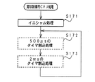
次に、表示制御用CPU101の動作を説明する。
図22は、表示制御基板80における表示制御用CPU101の動作を示すフローチャートである。表示制御用CPU101は、出力ポートやワークエリアの初期化およびタイマセット等のイニシャル処理を行った後に(ステップS101)、ループ状態に入る。イニシャル処理において、500μsおよび2ms毎にタイマ割込が発生するようなタイマ設定がなされている。よって、ループ状態では、500μsのタイマ割込がかかると500μsタイマ割込処理が行われ(ステップS102)、2msのタイマ割込がかかると2msタイマ割込処理が行われる(ステップS103)。なお、500μsタイマ割込処理では表示制御コマンド受信処理が行われ、2msタイマ割込処理では表示制御処理が実行される。
【0138】
図23は、2msのタイマ割込処理を示すフローチャートである。2msのタイマ割込がかかると、表示制御用CPU101は、次の2ms割込がかかるようにタイマを起動する等のイニシャル処理を行った後に(ステップS111)、表示制御プロセス処理(ステップS112)を実行する。
【0139】
図24は、500μsタイマ割込処理で実行される表示制御コマンド読込処理を示すフローチャートである。表示制御コマンド読込処理において、表示制御用CPU101は、ストローブ信号(INT信号)に割り当てられている入力ポートのビット7を読み込む。そして、ビット7がオン(ローレベル)しているか否か確認する(ステップS501)。オンしていれば、表示制御コマンドデータの入力に割り当てられている入力ポートから表示制御コマンドデータを読み取る(ステップS502)。なお、上述したように、INT信号は、主基板31のCPU56が新たな表示制御コマンドデータを出力したときにローレベルとされる。
【0140】
INT信号がオフしている場合には、表示通信カウンタをクリアする(ステップS506)。表示通信カウンタは、INT信号がオンしているときの表示制御コマンドデータ受信回数をカウントするために用いられる。
【0141】
INT信号がオンしている場合には、受信した表示制御コマンドデータが直前に(500μs前)受信したコマンドデータと同じか否か確認する(ステップS503)。同じでない場合には、表示通信カウンタをクリアする(ステップS506)。同じであった場合には、表示通信カウンタが所定の最大値(MAX)に達しているか否か確認する(ステップS504)。
【0142】
最大値に達していない場合には、表示通信カウンタの値を+1する(ステップS505)。ここで、最大値とは、表示制御コマンドデータを確実に受信したと判定する値(この例では3)よりも大きい値であり、例えば、4ms間での受信回数をカウントする等の目的で用いられる。
【0143】
次いで、表示制御用CPU101は、表示通信カウンタ後が「3」になったか否か確認する(ステップS507)。「3」になっている場合には、受信したデータを受信コマンド格納エリアに格納する(ステップS509)。そして、受信したデータをワークエリアに格納する(ステップS510)。なお、ワークエリアに格納されたデータは、次の割込処理において、ステップS503において用いられる。
【0144】
以上のように、表示制御用CPU101は、例えば3回連続して同一の表示制御コマンドデータを受信すると、確かに表示制御コマンドを受信したとして、通信終了フラグをセットする。そして、通信終了フラグがセットされると、受信コマンド格納エリアに格納された表示制御コマンドにもとづいて図柄の変動および背景・キャラクタの表示切替等の処理が行われる。
【0145】
図25は、図23に示されたタイマ割込処理における表示制御プロセス処理(ステップS112)を示すフローチャートである。表示制御プロセス処理では、表示制御プロセスフラグの値に応じてステップS720〜S870のうちのいずれかの処理が行われる。各処理において、以下のような処理が実行される。
【0146】
表示制御コマンド受信待ち処理(ステップS720):通信終了フラグのオンに応じて受信コマンドが設定されているワークエリアの内容を読み出して、変動時間を特定可能な表示制御コマンドを受信したか否か確認する。
【0147】
リーチ動作設定処理(ステップS750):受信した変動時間を特定可能な表示制御コマンドに対応した複数の変動パターンのうちのいずれのパターンを使用するのかを決定する。
【0148】
全図柄変動開始処理(ステップS780):左右中図柄の変動が開始されるように制御する。
【0149】
図柄変動中処理(ステップS810):変動パターンを構成する各変動状態(変動速度や背景、キャラクタ)の切替タイミングを制御するとともに、変動時間の終了を監視する。また、左右図柄の停止制御を行う。
【0150】
全図柄停止待ち設定処理(ステップS840):変動時間の終了時に、全図柄停止を指示する表示制御コマンドを受信していたら、図柄の変動を停止し最終停止図柄(確定図柄)を表示する制御を行う。
【0151】
大当り表示処理(ステップS870):変動時間の終了後、大当たり遊技中のラウンド表示や、確変大当り表示または通常大当り表示の制御を行う。
【0152】
図26は、表示制御用CPU101の割込処理を示すフローチャートである。表示制御基板80に搭載された電源監視用ICが電源電圧の低下を検出すると、表示制御用CPU101に割込がかかる。なお、割込端子に他の割込要因も入力されるような場合や電源電圧の低下の検出をより確実にしたい場合には、図9に示されているように入力ポートに電源監視用IC902の出力を導入し、割込処理において入力ポートのレベルを確認して電源電圧の低下による割込が発生したことを検知してもよい。
【0153】
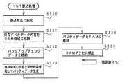
電源電圧の低下にもとづく割込処理では、まず、表示制御用CPU101は、割込禁止状態に設定する(ステップS330)。よって、以後、割込がかかることはない。従って、電源電圧低下中に表示制御用CPU101に複数回の割込がかかることはない。
【0154】
そして、表示制御用CPU101は、電源断時処理として、表示制御継続のために必要なデータをバックアップRAM領域に格納する(ステップS331)。また、バックアップRAM領域のバックアップチェックデータ領域に適当な初期値を設定し(ステップS332)、初期値およびバックアップRAM領域に退避させた全データについて順次排他的論理和をとって(ステップS333)、最終的な演算値をバックアップパリティデータ領域に設定する(ステップS334)。なお、チェックデータ生成の具体的処理は、主基板31のCPU56が実行する処理と同じでよい。
【0155】
さらに、表示制御用CPU101は、RAMアクセスを禁止状態にして(ステップS335)、以後、表示制御を停止する。停止状態は、遊技機への電力供給が再開されるまで継続する。
【0156】
図27は、図22に示されたメイン処理におけるイニシャル処理(ステップS101)の処理の一例を示すフローチャートである。遊技機への電力供給が再開されると、表示制御用CPU101にリセット信号が入力されて処理を再開するのであるが、イニシャル処理において、まず、電源投入時か否か確認する(ステップS341)。なお、表示制御用CPU101から見ると、不測の電源断後に遊技機への電力供給が再開されたときも電源投入時である。
【0157】
電源投入時であれば、RAMアクセス許可状態として(ステップS342)、バックアップRAM領域のデータチェック(この例ではパリティチェック)を行う(ステップS343)。不測の電源断が生じた後に復旧した場合には、バックアップRAM領域のデータは保存されていたはずであるから、チェック結果は正常になる。チェック結果が正常にならないのは、遊技店における営業開始時の電源投入時である。そこで、チェック結果が正常でなければ(ステップS344)、レジスタおよびRAM領域をクリアする(ステップS345)。また、必要な初期設定を行う。
【0158】
チェック結果が正常であれば(ステップS344)、バックアップRAM領域以外のデータをクリアする(ステップS346)。また、初期状態復帰要求待ちフラグをセットする(ステップS347)。
【0159】
ステップS341において電源投入時でないことが確認されると、表示制御用CPU101は、初期状態復帰要求待ちフラグがセットされているか否か確認する(ステップS350)。セットされていれば、主基板31から初期状態復帰要求コマンドを受信したか否か確認する(ステップS351)。受信していた場合には、RAMの内容等を初期状態に設定する(ステップS352)。そして、初期状態復帰要求待ちフラグをリセットするとともに(ステップS353)、遊技状態復帰要求待ちフラグをセットする(ステップS354)。
【0160】
ステップS350において初期状態復帰要求待ちでないことが確認されたら、表示制御用CPU101は、遊技状態復帰要求待ちフラグがセットされているか否か確認する(ステップS355)。セットされていれば、主基板31から遊技状態復帰要求コマンドを受信したか否か確認する(ステップS356)。受信していた場合には、バックアップRAM領域に保存されていたデータを本来の領域に復帰させる(ステップS357)。そして、遊技状態復帰要求待ちフラグをリセットする(ステップS358)。
【0161】
上述したように、主基板31のCPU56は、不測の電源断後に電源復旧したときに、初期状態復帰要求コマンドを送出してくる。よって、表示制御用CPU101は、そのコマンドを受信すると、ステップS352において内部状態を初期状態(遊技店における営業開始時の電源投入時の状態)に設定する。従って、表示制御プロセス処理等では、初期状態の設定にもとづく処理が行われる。すなわち、例えば、可変表示部9に初期画面の表示がなされる。
【0162】
その後、主基板31のCPU56は、遊技状態復帰要求コマンドを送出してくる。よって、表示制御用CPU101は、そのコマンドを受信すると、ステップS357において、内部状態を電源断時の状態に戻す。すると、表示制御プロセス処理等では、電源断時の状態から処理を再開することができる。
【0163】
なお、処理再開時に区切りのよい制御状態から再開してもよい。例えば、電源断時に可変表示部9において図柄の変動中であった場合には、変動開始の段階から表示制御を再開してもよい。電源断時に図柄の変動中であった場合には、バックアップRAM領域に保存されていた表示制御プロセスフラグは「図柄変動中」(図25参照)の値を示している。そこで、そのような場合には、表示制御用CPU101は、例えばステップS357において図柄の変動期間を計測するタイマの値を初期値(変動開始時の値)に戻す等の制御を行えば、変動開始の段階から表示制御を再開することができる。
【0164】
また、電源断時に可変表示部9において図柄の変動中であった場合には、変動結果を可変表示部9に表示して処理を先に進めてもよい。表示制御用CPU101は、例えば、バックアップRAM領域に保存されていた表示制御プロセスフラグが「図柄変動中」の値を示している場合には、バックアップRAM領域に保存されていた停止図柄保存領域の内容を可変表示部9に表示する制御を行うとともに、表示制御プロセスフラグの値を「表示制御コマンド受信待ち」に対応した値に設定すれば、変動結果を可変表示部9に表示して処理を先に進めることができる。
【0165】
さらに、バックアップRAM領域に保存されていた表示制御プロセスフラグが「大当り表示処理」(上述したように、大当り表示処理には、大当り遊技中の表示期間も含まれる)が示した場合には、表示制御用CPU101は、その処理状態に戻ることができる。このとき、主基板31のCPU56は、そのバックアップRAM領域に保存されていた特別図柄プロセスフラグが例えば「大入賞口開放中処理」を示していた場合には、その状態に戻る。従って、大入賞口が開放中であった場合には、主基板31のCPU56は、再度大入賞口を開放する制御を行う。また、大当り遊技中の所定のラウンド(電源断時におけるラウンド)から大当り遊技を再開することができる。なお、ラウンド数を示す情報や出力ポートの状態(例えば、大入賞口開放のためのソレノイド21に対する出力ポート)は、電源断時にバックアップRAM領域に保存される。
【0166】
また、電源断が「大入賞口開放中処理」時で大入賞口開放中に発生した場合には、所定のラウンドを示す情報だけでなく、RAMに記憶されているそのラウンドにおける開放経過時間および大入賞口入賞個数(カウント数)も保存されている。従って、主基板31のCPU56は、電源復旧時に、大入賞口開放経過時間およびカウント数についても電源断時の状態から再開することができる。
【0167】
図28は、主基板31から音声制御基板70に送出される音声制御コマンドデータの例を示す説明図である。図28に示す各音声制御コマンドデータは8ビットで構成され、それぞれ、効果音の種類を指定する。また、音声制御コマンドデータの中には、初期状態復帰要求コマンドと遊技状態復帰要求コマンドとがある。それらのコマンドは、主基板31のCPU56が表示制御基板80に初期状態復帰要求と遊技状態復帰要求の表示制御コマンドを送出するときに、音声制御基板70にも送出される。
【0168】
図29は、音声制御コマンドのビット構成を示す説明図である。図29に示すように、音声制御コマンドは、8ビットのデータと、1ビットのストローブ信号(INT信号)とから構成されている。
【0169】
図30は、図12に示されたメイン処理における出力データ設定処理(ステップS8)を示すフローチャートである。ただし、ここでは、音声制御基板70およびランプ制御基板35に対する制御コマンドの出力データ設定についてのみ示す。出力データ設定処理において、CPU56は、音声データに変更がないかどうか判定する(ステップS81)。音声データの変更は、例えば、主基板31のCPU56すなわち遊技制御手段の特別図柄プロセス処理において、音発生パターンの変更が必要とされるときに変更される。
【0170】
音声データに変更があった場合には、CPU56は、例えば特別図柄プロセス処理で使用されるプロセスデータ中の音声データすなわち音声制御コマンドデータを読み出す(ステップS82)。そして、ポートCデータ格納領域に設定する(ステップS84)。また、ポートC出力要求をセットする(ステップS85)。
【0171】
音声データに変更がなかった場合には、CPU56は、ランプデータに変更がないかどうか判定する(ステップS86)。ランプデータの変更も、例えば、遊技制御手段の特別図柄プロセス処理において、ランプ・LED表示パターンの変更が必要とされるときに変更される。
【0172】
ランプデータに変更があった場合には、CPU56は、例えば特別図柄プロセス処理で使用されるプロセスデータ中のランプデータすなわちランプ制御コマンドデータを読み出す(ステップS87)。そして、ポートEデータ格納領域に設定する(ステップS89)。また、ポートE出力要求をセットする(ステップS90)。
【0173】
図31は、図12に示されたメイン処理におけるデータ出力処理(ステップS6)の音声制御コマンド出力処理部分を示すフローチャートである。音声制御コマンド出力に関するデータ出力処理において、CPU56は、ポートC出力要求がセットされているか否か判定する(ステップS601)。ポートC出力要求がセットされている場合には、ポートC出力要求をリセットし(ステップS602)、ポートC格納領域の内容を出力ポート(出力ポートC)573に出力する(ステップS603)。ポートC格納領域のビット0〜7には音声制御コマンドデータが設定される。そして、ポートC出力カウンタを+1するとともに(ステップS604)、出力ポート(ポートD)574のビット7を0にする(ステップS605)。
【0174】
ポートC出力要求がセットされていない場合には、ポートC出力カウンタの値が0であるか否か判定する(ステップS606)。ポートC出力カウンタの値が0でない場合には、ポートC出力カウンタの値が2であるか否か確認する(ステップS607)。ポートC出力カウンタの値が2ではない、すなわち1である場合には、ポートC出力カウンタの値を1増やす(ステップS608)。
【0175】
ポートC出力カウンタの値が2である場合には、ポートC出力カウンタの値をクリアするとともに(ステップS609)、出力ポート(出力ポートD)574のビット7を1にする(ステップS610)。
【0176】
出力ポートDのビット7は、音声制御基板70に与えられるINT信号を出力するポートである。また、出力ポートCのビット0〜7は、音声制御コマンドデータを出力するポートである。そして、この実施の形態では、図31に示されたデータ出力処理は2msに1回実行される。従って、図31に示されたデータ出力処理によって、図32に示すように、音声制御コマンドデータが出力されるときに、4ms間INT信号がローレベルになる。
【0177】
次に、音声制御用CPU701の動作を説明する。
図33は、音声制御基板70における音声制御用CPU701の動作を示すフローチャートである。音声制御用CPU701は、出力ポートやワークエリアの初期化およびタイマセット等のイニシャル処理を行った後に(ステップS121)、ループ状態に入る。イニシャル処理において、500μsおよび2ms毎にタイマ割込が発生するようなタイマ設定がなされている。よって、ループ状態では、500μsのタイマ割込がかかると500μsタイマ割込処理が行われ(ステップS122)、2msのタイマ割込がかかると2msタイマ割込処理が行われる(ステップS123)。なお、500μsタイマ割込処理では音声制御コマンド受信処理が行われ、2msタイマ割込処理では音声制御処理が実行される。
【0178】
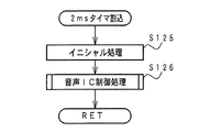
図34は、2msのタイマ割込処理を示すフローチャートである。2msのタイマ割込がかかると、音声制御用CPU701は、次の2ms割込がかかるようにタイマを起動する等のイニシャル処理を行った後に(ステップS125)、音声IC制御処理(ステップS126)を実行する。なお、500μsタイマ割込処理による音声制御コマンド受信処理は、表示制御用CPU101が実行する表示制御コマンド受信処理と同様に行われる(図24参照)。
【0179】
ROMには、図28に示された各音声制御コマンドデータに応じた音声を音声合成回路(音声合成用LSI;例えばディジタルシグナルプロセッサ)702に発生させるための制御データが格納されている。音声制御用CPU701は、受信した各音声制御コマンドデータに対応した制御データをROMから読み出す。
【0180】
この実施の形態では、音声合成回路702は、転送リクエスト信号(SIRQ)、シリアルクロック信号(SICK)、シリアルデータ信号(SI)および転送終了信号(SRDY)によって制御される。音声合成回路702は、SIRQがローレベルになると、SICKに同期してSIを1ビットずつ取り込み、SRDYがローレベルになるとそれまでに受信した各SIからなるデータを1つの音声再生用データと解釈する。従って、音声制御用CPU701は、SIRQをオン(ローレベル)にして(ステップS135)、ROMから読み出した制御データをSICKに同期してSIとして出力し(ステップS136)、出力が完了したらSRDYをローレベルにする(ステップS137)。音声合成回路702は、SIによって制御データを受信すると、受信した制御データに応じた音声を発生する。
【0181】
音声制御基板70にも、図9に示されたような電源監視用IC902が搭載されている。そして、電源監視用IC902が電源電圧の低下を検出すると、音声制御用CPU701に割り込みをかける。割り込みがかかると、音声制御用CPU701は、電源断時処理として、音声制御継続のために必要なデータをバックアップRAM領域に格納する。なお、具体的な電源断時処理は、表示制御用CPU101が実行する制御と同様である(図26参照)。
【0182】
よって、音声制御用CPU701も、イニシャル処理(ステップS121)において、表示制御用CPU101と同様に、バックアップRAM領域に保存されていたデータの復帰処理と、初期状態復帰要求コマンドおよび遊技状態復帰要求コマンドの受信処理を行う(図27参照)。
【0183】
主基板31のCPU56は、不測の電源断後に電源復旧したときに、音声制御基板70に対しても初期状態復帰要求コマンドを送出してくる。音声制御用CPU701は、そのコマンドを受信すると、内部状態を初期状態(遊技店における営業開始時の電源投入時の状態)に設定する。従って、初期状態の設定にもとづく処理が行われる。
【0184】
その後、主基板31のCPU56は、遊技状態復帰要求コマンドを送出してくる。音声制御用CPU701は、そのコマンドを受信すると、内部状態を電源断時の状態に戻す。よって、音声制御手段も、やはり、電源断時の状態から処理を再開することができる。
【0185】
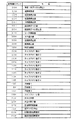
図36は、主基板31からランプ制御基板35に送出されるランプ制御コマンドの一例を示す説明図である。各ランプ制御コマンドデータは7ビットで構成され、それぞれ、遊技の進行に応じたランプ・LEDの点灯パターンおよび消灯を指定する。ただし、図36に示された例は、ある特定の遊技機に応じたパターンであって、他の機種の遊技機では、定義が異なる各ランプ制御コマンドデータが使用されうる。例えば、図36に示された例では特殊変動時ランプ指定が4種類(05H〜08H)あるが、特殊変動のパターンがそれよりも多い遊技機では、より多くの種類のランプ制御コマンドデータに特殊変動のパターンを割り当てればよい。あるいは、全ての遊技機で使用される可能性があるランプ制御データを定義しておき、そのうちから、各機種で必要に応じて使用するランプ制御データを選択するようにしてもよい。
【0186】
また、ランプ制御コマンドデータの中には、初期状態復帰要求コマンドと遊技状態復帰要求コマンドとがある。それらのコマンドは、主基板31のCPU56が表示制御基板80に初期状態復帰要求と遊技状態復帰要求の表示制御コマンドを送出するときに、ランプ制御基板35にも送出される。
【0187】
図37は、ランプ制御コマンドのビット構成を示す説明図である。図37に示すように、ランプ制御コマンドは、8ビットのデータと、1ビットのストローブ信号(INT信号)とから構成されている。
【0188】
図38は、図12に示されたメイン処理におけるデータ出力処理(ステップS6)のランプ制御コマンド出力処理部分を示すフローチャートである。ランプ制御コマンド出力に関するデータ出力処理において、CPU56は、ポートE出力要求がセットされているか否か判定する(ステップS621)。ポートE出力要求は、図30に示された出力データ設定処理において、ランプデータに変更があった場合にセットされる。
【0189】
ポートE出力要求がセットされている場合には、ポートE出力要求をリセットし(ステップS622)、ポートE格納領域の内容を出力ポート(出力ポートE)575に出力する(ステップS623)。ポートE格納領域のビット0〜7にはランプ制御コマンドデータが設定されている。そして、ポートC出力カウンタを+1するとともに(ステップS624)、出力ポート(ポートF)576のビット7を0にする(ステップS625)。
【0190】
ポートE出力要求がセットされていない場合には、ポートE出力カウンタの値が0であるか否か判定する(ステップS626)。ポートE出力カウンタの値が0でない場合には、ポートE出力カウンタの値が2であるか否か確認する(ステップS627)。ポートE出力カウンタの値が2ではない、すなわち1である場合には、ポートE出力カウンタの値を1増やす(ステップS628)。
【0191】
ポートE出力カウンタの値が2である場合には、ポートE出力カウンタの値をクリアするとともに(ステップS629)、出力ポート(出力ポートF)576のビット7を1にする(ステップS630)。
【0192】
出力ポートFのビット7は、ランプ制御基板35に与えられるINT信号を出力するポートである。また、出力ポートEのビット0〜7は、ランプ制御コマンドデータを出力するポートである。そして、この実施の形態では、図38に示されたデータ出力処理は2msに1回実行される。従って、図38に示されたデータ出力処理によって、図39に示すように、ランプ制御コマンドデータが出力されるときに、4ms間INT信号がローレベルになる。
【0193】
次に、ランプ制御用CPU351の動作を説明する。
図40は、ランプ制御基板35におけるランプ制御用CPU351の動作を示すフローチャートである。ランプ制御用CPU351は、出力ポートやワークエリアの初期化およびタイマセット等のイニシャル処理を行った後に(ステップS151)、ループ状態に入る。イニシャル処理において、500μsおよび2ms毎にタイマ割込が発生するようなタイマ設定がなされている。よって、ループ状態では、500μsのタイマ割込がかかると500μsタイマ割込処理が行われ(ステップS152)、2msのタイマ割込がかかると2msタイマ割込処理が行われる(ステップS153)。なお、500μsタイマ割込処理ではランプ制御コマンド受信処理が行われ、2msタイマ割込処理ではランプ制御処理が実行される。
【0194】
図41は、2msのタイマ割込処理を示すフローチャートである。2msのタイマ割込がかかると、ランプ制御用CPU351は、次の2ms割込がかかるようにタイマを起動する等のイニシャル処理を行った後に(ステップS155)、ランプ・LED点灯/消灯処理(ステップS156)を実行する。なお、500μsタイマ割込処理によるランプ制御コマンド受信処理は、表示制御用CPU101が実行する表示制御コマンド受信処理と同様に行われる(図24参照)。
【0195】
なお、ランプ制御用CPU351の内蔵ROMまたはランプ制御基板35に搭載された外付けROMには、各ランプ制御コマンドデータ(この例では、01H〜0FH)に応じた遊技効果LED28aおよび遊技効果ランプ28b,28cの点灯/消灯のパターンが、点灯パターンデータとして格納されている。そして、ランプ・LED点灯/消灯処理(ステップS156)では、受信したランプ制御コマンドに応じたテーブルの内容にもとづいてランプ・LEDの点灯/消灯制御を行う。また、ランプ制御コマンドに応じて賞球ランプ51および球切れランプ52の点灯/消灯処理を行う。
【0196】
ランプ制御基板35にも、図9に示されたような電源監視用IC902が搭載されている。そして、電源監視用IC902が電源電圧の低下を検出すると、ランプ制御用CPU351に割り込みをかける。割り込みがかかると、ランプ制御用CPU351は、電源断時処理として、ランプ・LED点灯/消灯制御継続のために必要なデータをバックアップRAM領域に格納する。なお、具体的な電源断時処理は、表示制御用CPU101が実行する制御と同様である(図26参照)。
【0197】
よって、ランプ制御用CPU351も、イニシャル処理(ステップS151)において、表示制御用CPU101と同様に、バックアップRAM領域に保存されていたデータの復帰処理と、初期状態復帰要求コマンドおよび遊技状態復帰要求コマンドの受信処理を行う(図27参照)。
【0198】
主基板31のCPU56は、不測の電源断後に電源復旧したときに、ランプ制御基板37に対しても初期状態復帰要求コマンドを送出してくる。ランプ制御用CPU371は、そのコマンドを受信すると、内部状態を初期状態(遊技店における営業開始時の電源投入時の状態)に設定する。従って、初期状態の設定にもとづく処理が行われる。
【0199】
その後、主基板31のCPU56は、遊技状態復帰要求コマンドを送出してくる。ランプ制御用CPU351は、そのコマンドを受信すると、内部状態を電源断時の状態に戻す。よって、ランプ制御手段も、やはり、電源断時の状態から処理を再開することができる。
【0200】
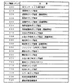
図42は、主基板31から賞球制御基板37に送出される賞球制御コマンドのビット構成の一例を示す説明図である。図42に示すように、ランプ制御コマンドは、8ビットのデータと、1ビットのストローブ信号(INT信号)とから構成されている。そして、8ビットのデータのうちの上位4ビットは制御指定として使用される。すなわち、ビット7,6,5,4が「0,0,0,0」であれば通常払出指定(賞球個数出力)を示し、「0,0,0,1」であれば補正払出指定を示し、「0,0,1,0」であれば球貸し禁止指定を示し、「0,1,1,1」であれば球貸し禁止指定解除を示す。なお、球貸し禁止指定は、余剰玉受皿4が満タンになって満タンスイッチ48がオンしたとき、および球切れ検出スイッチ167または球切れスイッチ187がオンしたときに、主基板31の基本回路53から送信される。そして、それらのスイッチがオフ状態になると、球貸し禁止指定解除が送信される。また、補正払出指定は、遊技制御手段が賞球払出不足を検出したときに主基板31から送出される。
【0201】
賞球制御コマンドは、主基板31から賞球制御基板37に、図8に示されたように、出力ポート(ポートG,H)577,578を介して送信される。そして、この実施の形態では、図43に示すように、主基板31から賞球制御コマンドデータが出力されるときに、4ms間INT信号がローレベルになる。
【0202】
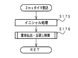
図44は、賞球制御基板37における賞球制御用CPU371の動作を示すフローチャートである。賞球制御用CPU371は、出力ポートやワークエリアの初期化およびタイマセット等のイニシャル処理を行った後に(ステップS171)、ループ状態に入る。イニシャル処理において、500μsおよび2ms毎にタイマ割込が発生するようなタイマ設定がなされている。よって、ループ状態では、500μsのタイマ割込がかかると500μsタイマ割込処理が行われ(ステップS172)、2msのタイマ割込がかかると2msタイマ割込処理が行われる(ステップS173)。なお、500μsタイマ割込処理では賞球制御コマンド受信処理が行われ、2msタイマ割込処理では賞球制御処理が実行される。
【0203】
図45は、2msのタイマ割込処理を示すフローチャートである。2msのタイマ割込がかかると、賞球制御用CPU371は、次の2ms割込がかかるようにタイマを起動する等のイニシャル処理を行った後に(ステップS175)、賞球処理(ステップS176)を実行する。なお、500μsタイマ割込処理による賞球制御コマンド受信処理は、表示制御用CPU101が実行する表示制御コマンド受信処理と同様に行われる(図24参照)。また、賞球制御処理では、賞球制御用CPU371は、主基板31から受信した賞球制御コマンドにもとづいて玉払出装置97を駆動して賞球払出を実行する。
【0204】
賞球制御基板37にも、図9に示されたような電源監視用IC902が搭載されている。そして、電源監視用IC902が電源電圧の低下を検出すると、賞球制御用CPU371に割り込みをかける。割り込みがかかると、賞球制御用CPU371は、電源断時処理として、賞球制御継続のために必要なデータをバックアップRAM領域に格納する。なお、具体的な電源断時処理は、表示制御用CPU101が実行する制御と同様である(図26参照)。
【0205】
よって、賞球制御用CPU371も、イニシャル処理(ステップS171)において、表示制御用CPU101と同様に、バックアップRAM領域に保存されていたデータの復帰処理を行う(図27参照)。ただし、初期状態復帰要求コマンドおよび遊技状態復帰要求コマンドの受信処理を行わない。
【0206】
以上のように、この実施の形態では、遊技機に対する電力供給が停止すると、主基板31、表示制御基板80、音声制御基板70、ランプ制御基板35および賞球制御基板37に搭載された各CPUは、割込処理によってそのことを認識し、必要なデータをバックアップRAM領域に転送する処理を行う。その際、チェックデータもバックアップRAM領域に設定する。よって、CPUは、不測の電源断からの復旧時に、バックアップRAM領域から必要なデータを復元することによって電源断時の状態から処理を再開することができる。
【0207】
上記の実施の形態では、各制御基板のCPUは、電源監視用IC902からの信号を割込端子または割込端子と入力ポートの双方に導入したが、入力ポートにのみ導入してもよい。図46は、そのような形態を示すブロック図である。図46におけるCPU901は、主基板31、表示制御基板80、音声制御基板70、ランプ制御基板35および賞球制御基板37に搭載された各CPUに相当する。この場合、主基板31において、CPU56は、割込処理ではなく、メイン処理において電源監視用ICからの信号がオン状態なったか否かを監視する。そして、オン状態になったことを検出すると、図13に示されたような必要なデータをバックアップRAMに保存する処理を行う。
【0208】
また、表示制御基板80、音声制御基板70、ランプ制御基板35および賞球制御基板37に搭載された各CPUは、割込処理ではなく、メイン処理(図22、図33、図40および図44に示された処理)におけるループ内で電源監視用ICからの信号がオン状態なったか否かを監視する。そして、オン状態になったことを検出すると、必要なデータをバックアップRAMに保存する処理を行う。
【0209】
なお、この実施の形態でも、各制御基板のCPUは、電源復旧したことを、初期リセット信号によって認識するようにしてもよいし、電源監視用IC902からの信号を導入する入力ポートのレベルによって認識するようにしてもよい。
【0210】
さらに、図47に示すように、電源監視用IC902からの信号を、CPU901のマスク不能割込端子(NMI端子)に導入してもよい。この場合、各制御基板において、CPUは、通常の割込処理ではなく、NMI処理において電源監視用ICからの信号がオン状態なったか否かを監視する。ただし、処理の内容は、割り込み禁止にする処理を除いて例えば図13に示された処理(必要なデータをバックアップRAMに保存する処理)と同じである。また、図47に示すように、電源監視用IC902からの信号を入力ポートにも導入し、NMI処理において、入力ポートのレベルが電源断を示している場合に必要なデータをバックアップRAMに保存する処理を行うようにしてもよい。また、CPUが、NMI端子のレベルが所定レベル(例えばローレベル)である状態でNMIがかかるようなものである場合には、電源監視用IC902とCPUのNMI端子との間に、NMI割込が1回のみかかるようなパルス幅のワンショットパルスを発生するワンショットパルス出力回路を設置してもよい。
【0211】
この場合にも、各制御基板のCPUは、電源復旧したことを、初期リセット信号によって認識するようにしてもよいし、電源監視用IC902からの信号を導入する入力ポートのレベルによって認識するようにしてもよい。
【0212】
なお、上記の各実施の形態では、電源電圧の低下を検出するために電源監視用IC902を用いたが、例えば、+12V電圧の分圧値をワンショットパルス出力回路に導入し、ワンショットパルス出力回路の出力を、割込端子(INT端子またはNMI端子)入力してもよい。ワンショットパルス出力回路は、入力レベルが所定値を下回るとワンショットパルスを出力するので、そのような構成でも、電源電圧の低下を検出することができる。
【0213】
さらに、ワンショットパルス出力回路の出力をCPUの入力ポートに導入して入力ポートのレベルを検知することによって電源電圧の低下を検出してもよいし、ワンショットパルス出力回路の出力を割込端子(INT端子またはNMI端子)と入力ポートとに入力してもよい。割込端子と入力ポートとに入力した場合には、割込処理において、入力ポートのレベルが検知され、そのレベルが電源断時のレベルを示していたら電源断時処理が実行される。
【0214】
また、上記の各実施の形態では、各制御基板に電源監視用IC902が搭載され、各制御基板において電源断の検出がなされたが、電源基板910に電源監視用ICを搭載し、電源基板910で一括して電源断の検出を行うように構成してもよい。その場合には、電源基板910から各制御基板に電源監視用ICからの検出信号が供給される。
【0215】
なお、以上の説明において、例えば図9に示されたように電源が復旧したことを初期リセット回路の出力によって検知してもよいことを示したが、例えば図4に示されているような定期リセット回路の出力が再開されたことをもって電源が復旧したことを検知してもよい。あるいは、CPUに対してその他のリセット手段が接続されている場合には、そのリセット手段を用いて電源が復旧したことを検知してもよい。
【0216】
上記の各実施の形態では、図9に示したように、遊技制御手段の復帰用データテーブルには、初期状態復帰要求コマンド、遊技状態復帰用タイマ値および遊技状態復帰要求コマンドを特定可能な情報が設定されていた。しかし、電源復旧時に、電源断時の遊技状態に容易に戻れるように、さらに多くの情報が設定されていてもよい。例えば、図48に示すように、特別図柄プロセスフラグ格納領域を指す情報(特別図柄プロセスフラグ設定領域)が復帰用データテーブルに設定されていてもよい。
【0217】
主基板31のCPU56は、電源復旧時に、例えば、復帰用データテーブルの特別図柄プロセスフラグ設定領域のデータを参照して特別図柄プロセスフラグの値を入力する。そして、その値にもとづいて電源断時の可変表示部9の図柄変動の状態を確認することができる。
【0218】
電源復旧時に、電源断時に可変表示部9で図柄変動中であった場合には図柄変動開始時の状態に戻ってもよいことは既に述べたが、そのような復帰を容易にするために、復帰用データテーブルにさらに多くのデータを設定してもよい。例えば、「全図柄変動開始処理」に対応した値を復帰用データテーブルに設定しておけば、CPU56は、その値を読み込んで、その値を特別図柄プロセスフラグに設定することによって、特別図柄の制御状態を「全図柄変動開始処理」に対応した状態に戻すことができる。なお、図19に示された特別図柄プロセス処理における「全図柄変動開始処理」では、表示制御基板80に対して、例えば、左右中最終停止図柄と変動態様を指令する情報とが送信される。
【0219】
ここでは、図柄変動開始時の状態に戻すことを容易にするためのデータとして、特別図柄プロセスフラグの「全図柄変動開始処理」に対応した値を例示したが、その他、特別図柄の制御状態を「全図柄変動開始処理」に対応した状態に戻すために他の内部フラグ等のワークデータの値を変更する必要がある場合には、それらの値も復帰用データテーブルに設定してしてもよい。
【0220】
このように、不測の電源断時に可変表示部9において図柄が変動中であって、電源復旧時に図柄変動開始時の状態に戻るように構成されている場合に、復帰用データテーブルにさらに多くの情報が設定されていると、遊技制御手段および表示制御手段は、容易にその状態に戻って復旧することができる。
【0221】
また、電源断時に図柄変動中であった場合、電源復旧時に遊技制御手段は電源断時の遊技状態に戻るとともに、表示制御手段は、所定の表示制御を行ってもよい。そのような制御を可能にするために、図48には、エラーコマンドも設定されている。なお、上述したように、電源断時に図柄変動中であった場合に、電源復旧時に遊技制御手段が図柄変動開始時の状態に戻るように構成されているときには、復帰用データテーブルにエラーコマンドが設定されている必要はない。
【0222】
図49は、主基板31のCPU56が実行するシステムチェック処理(メイン処理におけるステップS3)の他の例を示すフローチャートである。この例では、遊技状態復帰用タイマがタイムアウトしたときに(ステップS51)、CPU56は、特別図柄変動中であった否かを確認する(ステップS55)。その確認は、復帰用データテーブルにおける特別図柄プロセスフラグ設定領域の情報をアドレスとするRAM領域から、保存されていた特別図柄プロセスフラグを読み出すことによって実行可能である。特別図柄プロセスフラグが「全図柄停止待ち処理」を示していたら、CPU56は、特別図柄変動中であったと判断する。そして、特別図柄変動中であった場合には、表示制御基板80に対してエラーコマンド送出要求をセットする(ステップS56)。
【0223】
従って、表示制御用CPU101は、電源断時に可変表示部9において図柄変動中であった場合には、遊技状態復帰用タイマがタイムアウトしたときにエラーコマンドを受信することになる。表示制御用CPU101は、エラーコマンドを受信すると、図柄変動を再開するとともに、例えば可変表示部9にエラーであることを遊技者が識別しうるエラー表示を行う。そして、表示制御用CPU101は、図柄変動終了時にエラー表示を消去する。なお、表示制御用CPU101は、図柄変動を行わずエラー画面を表示してもよい。また、主基板31のCPU56は、特別図柄プロセスフラグの値を変更しない。すなわち、電源断時に図柄変動中であった場合、電源復旧時に遊技制御手段は電源断時の遊技状態に戻る。
【0224】
このような表示制御は、図柄変動開始時に遊技制御手段から表示制御手段に対して変動期間を特定可能な表示制御コマンドが送出され、以後、変動停止時まで表示制御コマンドが送出されないように構成された遊技機において効果的である。すなわち、図柄変動中には表示制御コマンドは送出されないので、遊技制御手段は、表示制御手段に対して、図柄変動中の途中の状態から遊技を再開させるような指示を行うことができない。遊技制御手段からの指示にもとづいて表示制御手段が図柄変動中の途中の状態から遊技を再開するように構成したい場合には、コマンド送出制御方式を変更しなければならない。しかし、上述したエラーコマンドを用いてその回の変動ではエラー画面を表示するように構成すれば、エラーコマンドを追加するだけで、コマンド送出制御方式(図柄変動開始時に遊技制御手段が表示制御手段に対して変動期間を特定可能な表示制御コマンドを送出する方式)を変更する必要はない。
【0225】
また、遊技制御手段が、電源断状態から電源断時の状態に復帰したときに、表示制御手段に対して、停止図柄(可変表示結果)を示す表示制御コマンドを送出するようにしてもよい。図50は、そのような処理を示すフローチャートである。この例では、遊技状態復帰用タイマがタイムアウトしたときに(ステップS51)、CPU56は、特別図柄変動中であった否かを確認する(ステップS55)。そして、特別図柄変動中であった場合には、表示制御基板80にして左右中図柄の停止図柄を示すコマンド送出要求をセットする(ステップS57)。
【0226】
表示制御用CPU101は、電源断時に図柄変動中であった場合には、遊技状態復帰用タイマがタイムアウトしたときに左右中図柄の停止図柄を示すコマンドを受信することになる。表示制御用CPU101は、左右中図柄の停止図柄を示すコマンドを受信すると、例えば図柄の可変表示を再開せず、可変表示部9に左右中図柄の停止図柄を表示する。なお、表示制御用CPU101は、その後に主基板31から送られてくる図柄変動停止を示すコマンドや大当り遊技の終了を示す表示制御コマンドを受信したらそれらのコマンドに従って通常の表示制御に戻る。
【0227】
なお、表示制御用CPU101は、左右中図柄の停止図柄を示すコマンドを受信すると、直ちにそれらの図柄を可変表示部9に表示してもよいし、本来の図柄変動期間の終了時(例えば、遊技制御手段から図柄確定のタイミングを示すコマンドを受信したとき)に停止図柄を可変表示部9に表示してもよい。また、本来の図柄変動期間の終了時に停止図柄を表示するように構成する場合に、遊技制御手段は、本来の図柄変動期間の終了時に左右中図柄の停止図柄を示すコマンドを送出してもよい。
【0228】
主基板31のCPU56は、電源復旧時に、バックアップRAM領域に保存されていた特別図柄プロセスフラグが例えば「全図柄停止待ち処理」を示していた場合には、その状態に復帰するのであるが、表示制御用CPU101は、その回の変動では、図柄変動制御を行わず可変表示結果を表示し続ける。従って、遊技者は、可変表示結果が表示されることによって停電から復旧したことを容易に認識できる。なお、可変表示結果が大当りである場合(停電前に行われた抽選結果が大当りであった場合)には、可変表示結果が表示し続けられた後に、遊技制御手段および表示制御手段ともに、大当たり遊技状態に復旧できるので、遊技者に不利益が与えられることはない。
【0229】
なお、停電等の不測の電源断を検出する電源監視手段の出力信号にもとづく必要データのバックアップ処理は、主基板31、表示制御基板80、音声制御基板70、ランプ制御基板35および賞球制御基板37の全てにおいて行われてもよいし、そのような制御を必要とする一部の基板において行われるようにしてもよい。例えば、主基板31のみでバックアップがなされていてもよい。また、遊技用装置を制御する遊技用装置制御手段を有する他の制御基板が存在する場合に、それらについても電源監視手段の出力信号にもとづくデータのバックアップ処理を行うようにしてもよい。
【0230】
電源バックアップがなされていない遊技用装置制御手段がある場合、遊技制御手段は、遊技状態復帰後に、遊技用装置制御手段をその遊技状態と合わせるために必要なコマンドを送出するようにしてもよい。例えば、表示制御手段がバックアップされていない場合、電源復旧時に特別図柄変動中の遊技状態に戻ったときには、遊技制御手段は、表示制御手段に対して例えば図柄変動の態様を示すコマンドと停止図柄を示すコマンド等を再度送出する。図柄変動を再開せず変動表示結果を表示させたいときには、例えば停止図柄を示すコマンドを再度送出する。
【0231】
【発明の効果】
以上のように、本発明によれば、遊技制御用マイクロコンピュータが、電源監視手段からの信号に応じて、電力供給が停止しているときにも内容を所定期間保持可能な遊技制御用バックアップRAMにデータを保存する処理を含む遊技制御用電源断時処理を実行し、払出制御用マイクロコンピュータが、電源監視手段からの信号に応じて、電力供給が停止しているときにも内容を所定期間保持可能な払出制御用バックアップRAMにデータを保存する処理を含む払出制御用電源断時処理を実行し、遊技制御用マイクロコンピュータが、さらに、電力供給が開始されたときに、遊技制御用電源断時処理が実行されていることを条件に、遊技状態を遊技制御用電源断時処理を開始したときの状態に復帰させるとともに、表示制御用マイクロコンピュータに対して、復帰コマンドを送出する復帰処理を実行し、表示制御用マイクロコンピュータが、復帰コマンドを受信したことに応じて可変表示部に遊技者が識別しうる復帰表示画面を表示するように構成したので、停電等の不測の電源断が発生したときに、必要なデータを保存して電源復旧時に電源断時の状態から遊技を再開できるとともに、遊技再開時に遊技制御用マイクロコンピュータおよび表示制御用マイクロコンピュータによる制御タイミングにずれが生じないようにすることができ、円滑に遊技が再開される効果がある。
【図面の簡単な説明】
【図1】 パチンコ遊技機を正面からみた正面図である。
【図2】 パチンコ遊技機の遊技盤を正面からみた正面図である。
【図3】 パチンコ遊技機を背面からみた背面図である。
【図4】 遊技制御基板(主基板)の回路構成例を示すブロック図である。
【図5】 表示制御基板の回路構成例を示すブロック図である。
【図6】 音声制御基板の回路構成例を示すブロック図である。
【図7】 ランプ制御基板の回路構成例を示すブロック図である。
【図8】 賞球制御基板の回路構成例を示すブロック図である。
【図9】 電源監視および電源バックアップのためのCPU周りの一構成例を示すブロック図である。
【図10】 電源基板の一構成例を示すブロック図である。
【図11】 他の構成の電源基板を制御基板とともに示すブロック図である。
【図12】 主基板における基本回路の動作を示すフローチャートである。
【図13】 主基板のCPUの割込処理を示すフローチャートである。
【図14】 メイン処理におけるシステムチェック処理を示すフローチャートである。
【図15】 バックアップパリティデータ作成方法を説明するための説明図である。
【図16】 主基板における基本回路のROMに設定されるテーブルの一構成例を示す説明図である。
【図17】 表示制御コマンドの構成例を示す説明図である。
【図18】 表示制御コマンドデータの構成例を示す説明図である。
【図19】 特別図柄プロセス処理のプログラムの一例を示すフローチャートである。
【図20】 表示制御データ出力処理を示すフローチャートである。
【図21】 表示制御コマンドデータの出力の様子を示すタイミング図である。
【図22】 表示制御用CPUが実行するメイン処理を示すフローチャートである。
【図23】 表示制御用CPUの2msタイマ割込処理を示すフローチャートである。
【図24】 表示制御用CPUの表示データ読込処理を示すフローチャートである。
【図25】 表示制御用CPUが実行する表示制御プロセス処理を示すフローチャートである。
【図26】 表示制御用CPUの割込処理を示すフローチャートである。
【図27】 表示制御用CPUが実行するイニシャル処理を示すフローチャートである。
【図28】 音声制御コマンドの例を示す説明図である。
【図29】 音声制御コマンドのビット構成を示す説明図である。
【図30】 音声制御基板およびランプ制御基板に対する出力データ設定処理を示すフローチャートである。
【図31】 データ出力処理の音声制御コマンド出力処理部分を示すフローチャートである。
【図32】 音声制御コマンドデータの出力の様子を示すタイミング図である。
【図33】 音声制御用CPUが実行するメイン処理を示すフローチャートである。
【図34】 音声制御用CPUの2msタイマ割込処理を示すフローチャートである。
【図35】 音声IC制御処理を示すフローチャートである。
【図36】 ランプ制御コマンドの一例を示す説明図である。
【図37】 ランプ制御コマンドのビット構成を示す説明図である。
【図38】 データ出力処理のランプ制御コマンド出力処理部分を示すフローチャートである。
【図39】 ランプ制御コマンドデータの出力の様子を示すタイミング図である。
【図40】 ランプ制御用CPUが実行するメイン処理を示すフローチャートである。
【図41】 ランプ制御用CPUの2msタイマ割込処理を示すフローチャートである。
【図42】 賞球制御コマンドのビット構成を示す説明図である。
【図43】 賞球制御コマンドデータの出力の様子を示すタイミング図である。
【図44】 賞球制御用CPUが実行するメイン処理を示すフローチャートである。
【図45】 賞球制御用CPUの2msタイマ割込処理を示すフローチャートである。
【図46】 電源監視および電源バックアップのためのCPU周りの他の構成例を示すブロック図である。
【図47】 電源監視および電源バックアップのためのCPU周りのさらに他の構成例を示すブロック図である。
【図48】 復帰用データテーブルの他の構成を示す説明図である。
【図49】 システムチェック処理の他の例を示すフローチャートである。
【図50】 システムチェック処理のさらに他の例を示すフローチャートである。
【符号の説明】
1 パチンコ遊技機
31 主基板
35 ランプ制御基板
37 賞球制御基板
53 基本回路
56 CPU
70 音声制御基板
80 表示制御基板
101 表示制御用CPU
351 ランプ制御用CPU
371 賞球制御用CPU
701 音声制御用CPU
901 CPU
902 電源監視用IC
910 電源基板
916 コンデンサ[0001]
BACKGROUND OF THE INVENTION
The present invention relates to a gaming machine such as a pachinko gaming machine, and in particular, when a game medium is launched into a game area by a player's operation and the game medium wins a prize area provided in the game area, a predetermined value is given to the player. A gaming machine that can be given and a special game value can be given to a player based on the result of the special game being in a predetermined mode by entering the game medium into the specific winning portion. .
[0002]
[Prior art]
As a gaming machine, a game medium such as a game ball is launched into a game area by a launching device, and when a game medium wins a prize area such as a prize opening provided in the game area, a predetermined number of prize balls are paid out to the player. There is something to be done. Further, a variable display unit capable of changing the display state is provided, and is configured to give a predetermined game value to the player when the display result of the variable display unit becomes a predetermined specific display mode There is.
[0003]
The display result of the variable display unit that displays the special symbol is a combination of a specific display mode that is determined in advance. Note that the game value is the right that the state of the variable winning ball device provided in the gaming area of the gaming machine is advantageous for a player who is likely to win a ball, or the advantageous state for a player. It is to generate.
[0004]
When the big hit occurs, for example, the big winning opening is opened a predetermined number of times, and the game shifts to a big hit gaming state where the hit ball is easy to win. And in each open period, if there is a prize for a predetermined number (for example, 10) of the big prize opening, the big prize opening is closed. And the number of times the special winning opening is opened is fixed to a predetermined number (for example, 16 rounds). An opening time (for example, 29.5 seconds) is determined for each opening, and even if the number of winnings does not reach a predetermined number, the big winning opening is closed when the opening time elapses. Further, when a predetermined condition (for example, winning in the V zone provided in the big prize opening) is not established at the time when the big prize opening is closed, the big hit gaming state is ended.
[0005]
In addition, among the combinations of display modes other than the “big hit” combination, the variable display in which the display result has already been derived and displayed at the stage where some of the display results of the plurality of variable display units have not yet been derived and displayed. A state in which the display mode of the part satisfies a display condition that is a combination of specific display modes is referred to as “reach”. Then, if the display result of the identification information variably displayed on the variable display portion does not satisfy the condition of “reach”, it becomes “missing”, and the variable display state ends. A player plays a game while enjoying how to generate a big hit.
[0006]
The game progress in the gaming machine is controlled by game control means such as a microcomputer. The identification information, character image, and background image displayed on the variable display device are controlled by display control means that operates in accordance with display control command data from the game control means. In general, the identification information, character image, and background image displayed on the variable display device are a display control microcomputer and a video display processor that generates image data in accordance with instructions from the microcomputer and transfers the image data to the variable display device side ( VDP), the program capacity of the display control microcomputer is large.
[0007]
Therefore, it is impossible to control identification information and the like displayed on the variable display device by the microcomputer of the game control means having a limited program capacity, and the display control microcomputer (separate from the microcomputer of the game control means) Display control means) is used. Therefore, the game control means for controlling the progress of the game needs to transmit a display control command to the display control means.
[0008]
In such a gaming machine, a speaker is provided on the game board, and various sound effects are emitted from the speaker as the game progresses in order to enhance the gaming effect. In addition, light emitters such as lamps and LEDs are provided on the game board, and these light emitters are turned on and off as the game progresses in order to enhance the gaming effect. Generally, sound control for generating sound effects is performed by game control means for controlling the progress of the game. Further, the lighting / extinguishing control of the light emitter is performed by a game control means for controlling the progress of the game. Then, if the model of the gaming machine is different, the method of generating the sound effect is different, and the pattern of lighting / extinguishing of the lamp and LED is different, so the configuration of the game control means must be changed accordingly. Therefore, if the models are different, it is necessary to redesign the game control means, and there is a problem that the design cost increases.
[0009]
In order to avoid such a problem, a sound control board equipped with sound control means is provided separately from the game control means, or a light emitter control board equipped with light emitter control means is provided separately from the game control means. Thus, the control command may be sent from the game control means to the sound control means or the light emitter control means as the game progresses. According to such a configuration, it is possible to cope with different models by changing the interpretation of the control command by the voice control unit and the light emitter control unit. The same configuration can be adopted when a control command is sent to each control board that is a board other than the voice control board and the light emitter control board and on which a control microprocessor (control means) is mounted. Note that changes in the interpretation of the control commands in each control means can be easily handled by software changes.
[0010]
Also, a player generally borrows game media through a gaming machine. In that case, a gaming medium lending mechanism is provided in the gaming machine. The game medium lending mechanism is often shared with a payout mechanism for paying out a prize ball. Even if the game media lending mechanism and the prize ball payout mechanism are shared or separately provided, both perform the operation of paying out the game media. It is controlled by prize ball control means mounted on the substrate.
[0011]
Since the progress of the game is controlled by game control means mounted on the main board, the number of winning balls based on winning is determined by the game control means and transmitted to the winning ball control board. On the other hand, the rental of game media is irrelevant to the progress of the game, and is generally controlled by the prize ball control means without going through the game control means.
[0012]
[Problems to be solved by the invention]
As described above, various control means are mounted on the gaming machine in addition to the game control means. Generally, each control means is constituted by a microcomputer. That is, a program is stored in a ROM or the like, and data temporarily generated for control or data that changes as control proceeds is stored in the RAM. Then, when the power-off state due to a power failure or the like occurs in the gaming machine, the data in the RAM is lost. Therefore, when recovering from a power outage or the like, the player must return to the initial state (for example, the state when the game machine was first turned on at the game store for the first time in the day), which may cause a disadvantage to the player. There is. For example, if a power failure occurs during a jackpot game and the gaming machine returns to the initial state, the player cannot enjoy the benefits based on the jackpot.
[0013]
In order to avoid such a situation, when an unexpected power cut such as a power failure occurs, the necessary data is saved in the power backup RAM, and the data saved when the power is restored is restored. Can be resumed. However, as described above, the game control is executed by the game control means mounted on the main board, but the various game control devices provided in the gaming machine are connected to other control boards different from the main board. It is controlled by each mounted control means. Since the starting method of each control means at the time of power restoration generally varies, there is a possibility that a difference in control by the control means on each control board occurs at the time of power restoration.
[0014]
Therefore, the present invention can save the necessary data and resume the game from the power-off state when the power is restored when an unexpected power-off such as a power failure occurs, and control means on each control board when the game resumes It is an object of the present invention to provide a gaming machine that does not cause a deviation in control timing due to the above.
[0015]
[Means for Solving the Problems]
The gaming machine according to the present invention predetermines whether the display result of the identification information displayed on the variable display unit is a predetermined specific display mode based on the winning of the game medium to the specific winning unit, A gaming machine that controls the gaming state advantageous to the player based on the fact that the display result of the identification information is determined to be a specific display mode, and controls the progress of the game and starts the fluctuation of the identification information A game control board equipped with a game control microcomputer that transmits a command that can specify a change time when the change time ends, and a command that indicates a stop time of change of identification information when the change time ends, and a game control When a command that can specify the change time is received from the microcomputer for the game, the change of the identification information is started on the variable display unit, and the change of the identification information from the game control microcomputer is started And a display control board display control microcomputer for controlling to stop the change of the identification information is mounted in the variable display unit when receiving a command indicating termination timing, A payout control board equipped with a payout control microcomputer that controls payout means for paying out game media based on the fact that the payout condition is satisfied; In response to detecting a predetermined amount of voltage drop by monitoring the power supply voltage drop of the gaming machine signal Output One Power supply monitoring means, The signal from the power supply monitoring means is input to the game control board and the payout control board, The game control microcomputer can retain the contents for a predetermined period even when the power supply is stopped according to the signal from the power supply monitoring means. For game control Includes processing to save data to backup RAM For game control Performs power-off processing The payout control microcomputer, according to a signal from the power supply monitoring means, includes a process of storing data in a payout control backup RAM capable of holding the contents for a predetermined period even when the power supply is stopped. The control power-off process is executed, and the game control microcomputer further includes: When power supply is started, For game control The game state is changed on condition that the power-off process is executed. For game control In addition to returning to the state when the power-off process was started, the display control microcomputer ,return The display control microcomputer that executes the return process to send the command return The player can identify the variable display in response to receiving the command. return Display the display screen Do It is characterized by that.
[0023]
DETAILED DESCRIPTION OF THE INVENTION
Hereinafter, an embodiment of the present invention will be described with reference to the drawings.
First, the overall configuration of a pachinko gaming machine that is an example of a gaming machine will be described. 1 is a front view of the
[0024]
As shown in FIG. 1, the
[0025]
Near the center of the
[0026]
An open /
[0027]
The
[0028]
In this example, a
[0029]
In addition, a
[0030]
The
[0031]
The hit ball fired from the hit ball launching device enters the
[0032]
The rotation of the image in the
[0033]
When the combination of images in the
[0034]
Next, the structure of the back surface of the
On the back surface of the
[0035]
The
[0036]
FIG. 3 is a rear view of the game board of the
[0037]
In order to perform prize ball payout control, signals from a winning ball detection switch (not shown), the
[0038]
FIG. 4 is a block diagram illustrating an example of a circuit configuration in the
[0039]
Further, a
[0040]
Further, according to the data given from the
[0041]
The
[0042]
Further, an initial reset circuit 65 for resetting the
Note that there is also switch information input to the
[0043]
A ball hitting device for hitting and launching a game ball is driven by a drive motor 94 controlled by a circuit on the
[0044]
FIG. 5 is a block diagram showing a circuit configuration in the
[0045]
The display control CPU 101 operates in accordance with a program stored in the control data ROM 102. When a strobe signal is input from the
[0046]
Then, the display control CPU 101 performs display control of the screen displayed on the
[0047]
5 also shows a
[0048]
The
[0049]
FIG. 6 is a block diagram showing a configuration example of the voice control command signal transmission portion of the
[0050]
As shown in FIG. 6, the voice control command is output from the output ports (output ports C and D) 573 and 574 of the I /
[0051]
Then, for example, a
[0052]
As the
[0053]
In addition, a
[0054]
FIG. 7 is a block diagram showing signal transmission / reception portions in the
[0055]
As shown in FIG. 7, the lamp control command related to the lamp control is output from the output ports (output ports E and F) 575 and 576 of the I /
[0056]
In the
[0057]
On the
[0058]
As the
[0059]
In the configuration shown in FIG. 7, it is possible to eliminate a signal line that may give a signal from the
[0060]
Further, a
[0061]
In FIG. 7, a signal instructing to turn on or off the
[0062]
FIG. 8 is a block diagram showing components related to the prize ball, such as components of the prize
[0063]
Detection signals from the ball
[0064]
When the detection signal from the ball
[0065]
Further, a detection signal from the prize ball count switch 301 </ b> A is also input to the I /
[0066]
When there is a prize, a prize ball control command indicating the number of prize balls is input to the prize
[0067]
Each buffer in the input buffer circuit 373 can pass a signal only in the direction from the
[0068]
In addition, a
[0069]
Further, the prize ball control CPU 371 outputs a ball lending number signal indicating the number of lending balls to the
[0070]
Further, the detection signal of the prize
[0071]
The
[0072]
A ball lending switch signal and a return switch signal are given from the balance display board 74 to the
[0073]
When the power of the
[0074]
As described above, all signals from the
[0075]
In this embodiment, the CPU 56, the display control CPU 101, the
[0076]
FIG. 9 is a block diagram illustrating an example of a configuration around the CPU for power supply monitoring and power supply backup. As shown in FIG. 9, the power
[0077]
Further, as shown in FIG. 9, the
[0078]
The predetermined value for the
[0079]
While the power is not supplied from the + 5V power supply, the
[0080]
Here, the normal reset state is restored by the reset signal from the
[0081]
The configuration shown in FIG. 9 is applied to each gaming device control board (in this embodiment, the
[0082]
FIG. 10 is a block diagram illustrating a configuration example of the
[0083]
The transformer 911 converts AC voltage from the AC power source into 24V. The AC 24V voltage is output to the
[0084]
The + 5V line from the DC-DC converter 913 branches to form a backup + 5V line. A large-
[0085]
A battery that can be charged from a + 5V power supply may be used as the backup power supply. In the case of using a battery, a rechargeable battery is used in which the capacity disappears when a state in which no power is supplied from the +5 V power source continues for a predetermined time.
[0086]
FIG. 11 is a block diagram showing a
[0087]
The
[0088]
In the
[0089]
When the + 5V voltage used in each control board is generated collectively by the
[0090]
Next, the operation of the gaming machine will be described.
FIG. 12 is a flowchart showing the operation of the CPU 56 in the
[0091]
Next, the CPU 56 performs a stack setting process for setting the designated address of the stack pointer (step S2). In this example, 00FFH is set in the stack pointer. Then, a system check process is performed (step S3). In the system check process, the CPU 56 determines whether or not an error is included in the RAM 55. If the error is included, the CPU 56 performs a process such as initializing the RAM 55. Further, when power is turned on, control is also performed to restore the register contents saved in the backup RAM area.
[0092]
Next, after performing a process of setting a display control command sent to the
[0093]
Next, a process of outputting the contents of the storage area for various output data to each output port is performed (data output process: step S6). Further, an output data setting process for setting output data such as jackpot information, start information, probability variation information, etc., output to the hall management computer in the storage area is performed (step S8). Further, various abnormality diagnosis processes are performed by the self-diagnosis function provided in the
[0094]
Next, a process of updating each counter indicating each determination random number such as a big hit determination random number used for game control is performed (step S10).
[0095]
Next, the CPU 56 performs special symbol process processing (step S11). In the special symbol process control, corresponding processing is selected and executed according to a special symbol process flag for controlling the
[0096]
Further, the CPU 56 inputs the states of the gate sensor 12, the
[0097]
The CPU 56 further performs a process of updating a display random number such as a random number that determines the type of stop symbol (step S15).
[0098]
Further, the CPU 56 performs signal processing with the prize ball control board 37 (step S16). That is, when a predetermined condition is satisfied, a prize ball control command is output to the prize
[0099]
FIG. 13 is a flowchart showing the interrupt process of the CPU 56. As described above, when the power
[0100]
In the interrupt process based on the decrease in the power supply voltage, first, the CPU 56 sets the interrupt prohibited state (step S20). Therefore, no interruption is applied thereafter. Therefore, the CPU 56 is not interrupted a plurality of times during the power supply voltage drop.
[0101]
Then, the CPU 56 stores the contents of each register in the backup RAM area as a power-off process (step S21). Also, an appropriate initial value is set in the backup check data area of the backup RAM area (step S22), and exclusive OR is sequentially performed on the initial value and all the data saved in the backup RAM area (step S23), and finally An arithmetic value is set in the backup parity data area (step S24).
[0102]
Further, the CPU 56 lights the
[0103]
Then, the CPU 56 disables the RAM access (step S26), and thereafter stops the game control. The stop state continues until power supply to the gaming machine is resumed.
[0104]
FIG. 14 is a flowchart showing an example of the system check process (step S3) in the main process shown in FIG. When power supply to the gaming machine is resumed, an initial reset signal is input from the initial reset circuit 65 to the CPU 56. The CPU 56 starts the main process in response to the initial reset signal. In the system check process, first, it is confirmed whether or not the power is turned on (step S41). From the viewpoint of the CPU 56, the power is also turned on when the power supply to the gaming machine is resumed after an unexpected power failure.
[0105]
If the power is turned on, the RAM access permission state is set (step S42). Then, a data check (parity check in this example) of the backup RAM area is performed (step S43). In the case of recovery after an unexpected power failure, the data in the backup RAM area should have been saved, so the check result is normal. In general, the check result does not become normal when power is turned on at the start of business in an amusement store. Therefore, if the check result is not normal (step S44), the register and the RAM area are cleared (step S45). Also, make necessary initial settings.
[0106]
If the check result is normal (step S44), only register clear is performed (step S46). Further, if necessary, an area other than the backup RAM area (an area that does not need to be saved at the time of restoration by turning off the power) is also cleared. The purpose of register clearing is to temporarily return to the initial state (the state when power is turned on at the start of business in the amusement store). As will be described later, after a certain period of time, the register state becomes an unexpected power supply. It will be returned to the state when it was interrupted.
[0107]
Then, the CPU 56 performs control to send an initial state return request command to the
[0108]
If it is confirmed in step S41 that the power is not turned on, the CPU 56 checks whether or not the gaming state return timer is operating (step S50). If it is in operation, it is confirmed whether or not a timeout has occurred (step S51). If timed out, control is performed to send a game state return request command to the
[0109]
FIG. 15 is an explanatory diagram for explaining a backup parity data creation method. However, in the example shown in FIG. 15, for simplification, the size of data saved in the backup data RAM area is 3 bytes. In the interrupt process due to the power supply voltage drop, as shown on the left side of FIG. 15, initial data (00H in this example) is set in the backup check data area. Next, an exclusive logical sum of “00H” and “F0H” is taken, and an exclusive logical sum of “16H” is obtained. Further, an exclusive OR of the result and “DFH” is taken. Then, the result (“39H” in this example) is set in the backup parity data area.
[0110]
When the power is turned on again, parity diagnosis is performed in step S43 shown in FIG. 14, and the right side of FIG. 15 is an explanatory diagram showing an example of parity diagnosis. If all the data in the backup area is stored as it is, the data shown on the left side of FIG. 15 is set in the backup area when the power is turned on again.
[0111]
In the processing of step S813, the CPU 56 sequentially performs exclusive OR for each data in the backup data area using the data (in this example, “39H”) set in the backup parity data area in the backup RAM area as initial data. Process. If all the data in the backup area is stored as it is, the final calculation result matches “00H”, that is, the data set in the backup check data area. If a bit error has occurred in the data in the backup RAM area, the final calculation result is not “00H”.
[0112]
Therefore, the CPU 56 compares the final calculation result with the data set in the backup check data area, and if they match, the parity diagnosis is normal. If they do not match, the parity diagnosis is abnormal.
[0113]
As described above, in this embodiment, when the power supply to the gaming machine is stopped, the CPU 56 recognizes this by an interrupt process and performs a process of saving necessary data in the backup RAM area. At that time, check data is also set in the backup RAM area. Therefore, the CPU 56 can confirm whether or not the data has been correctly stored when recovering from an unexpected power failure. Further, in the interrupt process, an interrupt prohibited state is set and a RAM access prohibited state is set. Therefore, when the power is cut off, multiple interruptions do not occur, and when the power supply voltage is lowered, the state of the bus line of the CPU 56 becomes indefinite. It is never done. A CPU used in a gaming machine generally has a RAM access prohibiting function.
[0114]
Further, as will be described later, the CPU on each control board other than the
[0115]
In this embodiment, the operation state of the CPU 56 is resumed by the initial reset signal, and until that time, the CPU 56 does not perform the normal game control. However, during the power backup, the CPU 56 is connected to the input port (for power monitoring). The state of the port) to which the signal from the
[0116]
FIG. 16 is an explanatory diagram showing a configuration example of a table set in the ROM 55. As shown in FIG. 16, the ROM 55 is provided with, for example, a restoration data table and an initial state data table. The return data table includes, for example, an initial state return command to be sent to each of the
[0117]
As described above, the return data table stores, in a recognizable manner, the commands sent to each of a plurality of gaming device control means (means for controlling the gaming device) when the power is restored. The CPU 56 of the
[0118]
FIG. 17 is an explanatory diagram of a configuration example of the display control command. As shown in FIG. 17, the display control command is composed of 8-bit data and a 1-bit strobe signal (INT signal).
[0119]
FIG. 18 is an explanatory diagram illustrating a configuration example of display control command data using 8-bit data. As shown in FIG. 18, for example, the type of control is instructed by the upper 4 bits of the 8 bits, and the specific control content is instructed by the lower 4 bits. For example, in this example, if the upper 4 bits are [0, 0, 0, 1], the reach type, stop all symbols, etc. are instructed by the lower 4 bits. If the upper 4 bits are [1, 0, 0, 0], [1, 0, 0, 1] or [1, 0, 1, 0], the lower 4 bits are numerically displayed on the
[0120]
If the upper 4 bits are [1, 1, 1, 0], it indicates an initial state return command. If the upper 4 bits are [1, 1, 1, 1], it indicates a game state return command. In these commands, the lower 4 bits are set to 0, for example.
[0121]
FIG. 19 is a flowchart showing an example of a special symbol process processing program executed by the CPU 56. The special symbol process shown in FIG. 19 is a specific process of step S11 in the flowchart of FIG. When performing the special symbol process, the CPU 56 performs any one of steps S300 to S309 shown in FIG. 19 according to the value of the special symbol process flag. In each process, the following process is executed.
[0122]
Special symbol variation waiting process (step S300): Waiting for the
[0123]
Special symbol determination process (step S301): When variable symbol special display can be started, the number of start winning memories is confirmed. If the starting winning memorized number is not 0, it is determined whether to win or not depending on the value of the extracted jackpot determination random number.
Stop symbol setting process (step S302): The stop symbol of the middle left and right symbols is determined.
[0124]
Reach operation setting process (step S303): It is determined whether or not a reach operation is performed according to the value of the reach determination random number, and a variation mode of the reach operation is determined according to the value of the reach operation random number.
[0125]
All symbol variation start processing (step S304): Control is performed so that the
[0126]
All symbols stop waiting process (step S305): When a predetermined time has elapsed, control is performed so that all symbols displayed on the
[0127]
Big hit display process (step S306): When the stop symbol is a combination of big hit symbols, control is performed so that display control command data for the big hit display is sent to the
[0128]
Big winning opening opening process (step S307): Control for opening the big winning opening is started. Specifically, the counter and the flag are initialized, and the
[0129]
Processing for opening a special prize opening (step S308): Control for sending display control command data for the big prize opening round display to the
[0130]
Jackpot end process (step S309): A display for notifying the player that the jackpot gaming state has ended is performed. When the display is completed, the internal flag and the like are returned to the initial state, and the internal state is updated to shift to step S300.
[0131]
The module (step S5 in FIG. 12) that performs the process of sending the display control command in the game control program according to the process of each step described above outputs the corresponding display control command data to the output port and outputs the strobe signal. Turn on.
[0132]
FIG. 20 is a flowchart showing the display control data output process (step S5) in the main process shown in FIG. In the display control data output process, the CPU 56 determines whether or not a port A output request is set (step S581). The port A output request is set in response to a command output request from a special symbol process or the like in the display control data setting process (step S4).
[0133]
If the port A output request is set, the port A output request is reset (step S582), and the contents of the port A storage area are output to the output port (output port A) 571 (step S583). Further, the port A output counter is incremented by 1 (step S584), and
[0134]
If the port A output request is not set, it is determined whether or not the value of the port A output counter is 0 (step S586). If the value of the port A output counter is not 0, it is confirmed whether or not the value of the port A output counter is 2 (step S587). When the value of the port A output counter is not 2, that is, 1, the value of the port A output counter is incremented by 1 (step S588).
[0135]
When the value of the port A output counter is 2, the value of the port A output counter is cleared (step S589), and
[0136]
[0137]
Next, the operation of the display control CPU 101 will be described.
FIG. 22 is a flowchart showing the operation of the display control CPU 101 in the
[0138]
FIG. 23 is a flowchart showing a 2 ms timer interrupt process. When a 2 ms timer interrupt is applied, the display control CPU 101 performs an initial process such as starting a timer so that the next 2 ms interrupt is applied (step S111), and then performs a display control process (step S112). Execute.
[0139]
FIG. 24 is a flowchart showing the display control command read process executed in the 500 μs timer interrupt process. In the display control command reading process, the display control CPU 101 reads
[0140]
If the INT signal is off, the display communication counter is cleared (step S506). The display communication counter is used to count the number of display control command data receptions when the INT signal is on.
[0141]
If the INT signal is on, it is checked whether or not the received display control command data is the same as the command data received immediately before (500 μs before) (step S503). If they are not the same, the display communication counter is cleared (step S506). If they are the same, it is confirmed whether or not the display communication counter has reached a predetermined maximum value (MAX) (step S504).
[0142]
If the maximum value has not been reached, the value of the display communication counter is incremented by 1 (step S505). Here, the maximum value is a value larger than the value (3 in this example) that is determined to have received display control command data reliably, and is used for the purpose of, for example, counting the number of receptions in 4 ms. It is done.
[0143]
Next, the display control CPU 101 checks whether or not the value after the display communication counter is “3” (step S507). If it is “3”, the received data is stored in the received command storage area (step S509). Then, the received data is stored in the work area (step S510). Note that the data stored in the work area is used in step S503 in the next interrupt process.
[0144]
As described above, for example, when the display control CPU 101 receives the same display control command data three times in succession, the display control command 101 sets the communication end flag on the assumption that the display control command has been received. When the communication end flag is set, processing such as symbol change and background / character display switching is performed based on the display control command stored in the received command storage area.
[0145]
FIG. 25 is a flowchart showing the display control process (step S112) in the timer interrupt process shown in FIG. In the display control process process, any one of steps S720 to S870 is performed according to the value of the display control process flag. In each process, the following process is executed.
[0146]
Display control command reception waiting process (step S720): Reads the contents of the work area where the reception command is set in response to the communication end flag being turned on, and confirms whether or not a display control command capable of specifying the variation time has been received To do.
[0147]
Reach operation setting process (step S750): It is determined which one of a plurality of variation patterns corresponding to the display control command capable of specifying the received variation time is to be used.
[0148]
All symbol variation start processing (step S780): Control is performed so that variation of the left and right middle symbols is started.
[0149]
Symbol variation processing (step S810): Controls the switching timing of each variation state (variation speed, background, character) constituting the variation pattern, and monitors the end of the variation time. In addition, stop control of the left and right symbols is performed.
[0150]
All symbol stop waiting setting process (step S840): When a display control command for instructing all symbols to stop is received at the end of the variation time, control for stopping the symbol variation and displaying the final stop symbol (determined symbol) is performed. Do.
[0151]
Big hit display processing (step S870): After the end of the variation time, the round display during the big hit game, the probability variable big hit display or the normal big hit display is controlled.
[0152]
FIG. 26 is a flowchart showing the interrupt processing of the display control CPU 101. When the power supply monitoring IC mounted on the
[0153]
In the interrupt process based on the decrease in the power supply voltage, the display control CPU 101 first sets the interrupt prohibited state (step S330). Therefore, no interruption is applied thereafter. Therefore, the display control CPU 101 is not interrupted a plurality of times during the power supply voltage drop.
[0154]
Then, the display control CPU 101 stores data necessary for continuation of display control in the backup RAM area as a power-off process (step S331). Also, an appropriate initial value is set in the backup check data area of the backup RAM area (step S332), and exclusive OR is sequentially obtained for the initial value and all data saved in the backup RAM area (step S333), and the final An arithmetic value is set in the backup parity data area (step S334). The specific process for generating check data may be the same as the process executed by the CPU 56 of the
[0155]
Further, the display control CPU 101 disables the RAM access (step S335), and thereafter stops the display control. The stop state continues until power supply to the gaming machine is resumed.
[0156]
FIG. 27 is a flowchart showing an example of the initial process (step S101) in the main process shown in FIG. When the power supply to the gaming machine is resumed, a reset signal is input to the display control CPU 101 and the process is resumed. In the initial process, first, it is confirmed whether or not the power is turned on (step S341). From the viewpoint of the display control CPU 101, the power supply is also turned on when power supply to the gaming machine is resumed after an unexpected power failure.
[0157]
If the power is turned on, the RAM access permission state is set (step S342), and data check (parity check in this example) of the backup RAM area is performed (step S343). In the case of recovery after an unexpected power failure, the data in the backup RAM area should have been saved, so the check result is normal. The check result does not become normal when power is turned on at the start of business at an amusement store. Therefore, if the check result is not normal (step S344), the register and the RAM area are cleared (step S345). Also, make necessary initial settings.
[0158]
If the check result is normal (step S344), data other than the backup RAM area is cleared (step S346). Also, an initial state return request wait flag is set (step S347).
[0159]
If it is confirmed in step S341 that the power is not turned on, the display control CPU 101 confirms whether or not the initial state return request wait flag is set (step S350). If it is set, it is confirmed whether or not an initial state return request command has been received from the main board 31 (step S351). If it has been received, the contents of the RAM and the like are set to the initial state (step S352). Then, the initial state return request wait flag is reset (step S353), and the game state return request wait flag is set (step S354).
[0160]
If it is confirmed in step S350 that it is not waiting for the initial state return request, the display control CPU 101 checks whether or not the game state return request wait flag is set (step S355). If set, it is confirmed whether or not a game state return request command is received from the main board 31 (step S356). If received, the data stored in the backup RAM area is restored to the original area (step S357). Then, the game state return request wait flag is reset (step S358).
[0161]
As described above, the CPU 56 of the
[0162]
Thereafter, the CPU 56 of the
[0163]
Note that when the process is resumed, the control state may be resumed with a good separation. For example, if the symbol is changing in the
[0164]
If the symbol is changing on the
[0165]
In addition, if the display control process flag stored in the backup RAM area indicates “big hit display process” (as described above, the big hit display process includes the display period during the big hit game), the display is performed. The control CPU 101 can return to the processing state. At this time, if the special symbol process flag stored in the backup RAM area indicates, for example, “a big prize opening opening process”, the CPU 56 of the
[0166]
In addition, when the power interruption occurs during the “opening process for opening the big prize opening” and during the opening of the big prize opening, not only information indicating a predetermined round but also the elapsed elapsed time in the round stored in the RAM and The number of winning prizes (counts) is also stored. Therefore, the CPU 56 of the
[0167]
FIG. 28 is an explanatory diagram showing an example of voice control command data sent from the
[0168]
FIG. 29 is an explanatory diagram showing a bit configuration of a voice control command. As shown in FIG. 29, the voice control command is composed of 8-bit data and a 1-bit strobe signal (INT signal).
[0169]
FIG. 30 is a flowchart showing the output data setting process (step S8) in the main process shown in FIG. However, only output data setting of control commands for the
[0170]
If there is a change in the voice data, the CPU 56 reads out the voice data in the process data used in the special symbol process, for example, the voice control command data (step S82). Then, the port C data storage area is set (step S84). Also, a port C output request is set (step S85).
[0171]
If there is no change in the audio data, the CPU 56 determines whether or not the lamp data is changed (step S86). The change of the lamp data is also changed, for example, when the change of the lamp / LED display pattern is required in the special symbol process of the game control means.
[0172]
When the lamp data is changed, the CPU 56 reads out lamp data, that is, lamp control command data in the process data used in the special symbol process, for example (step S87). Then, the port E data storage area is set (step S89). Also, a port E output request is set (step S90).
[0173]
FIG. 31 is a flowchart showing the voice control command output processing portion of the data output processing (step S6) in the main processing shown in FIG. In the data output processing related to the voice control command output, the CPU 56 determines whether or not the port C output request is set (step S601). If the port C output request is set, the port C output request is reset (step S602), and the contents of the port C storage area are output to the output port (output port C) 573 (step S603). Voice control command data is set in
[0174]
If the port C output request is not set, it is determined whether or not the value of the port C output counter is 0 (step S606). If the value of the port C output counter is not 0, it is confirmed whether or not the value of the port C output counter is 2 (step S607). When the value of the port C output counter is not 2, that is, 1, the value of the port C output counter is incremented by 1 (step S608).
[0175]
When the value of the port C output counter is 2, the value of the port C output counter is cleared (step S609), and
[0176]
[0177]
Next, the operation of the
FIG. 33 is a flowchart showing the operation of the
[0178]
FIG. 34 is a flowchart showing a 2 ms timer interrupt process. When a 2 ms timer interrupt is applied, the
[0179]
The ROM stores control data for causing a speech synthesis circuit (speech synthesis LSI; for example, a digital signal processor) 702 to generate speech corresponding to each speech control command data shown in FIG. The
[0180]
In this embodiment, the
[0181]
A
[0182]
Therefore, the
[0183]
The CPU 56 of the
[0184]
Thereafter, the CPU 56 of the
[0185]
FIG. 36 is an explanatory diagram showing an example of a lamp control command sent from the
[0186]
The lamp control command data includes an initial state return request command and a gaming state return request command. These commands are also sent to the
[0187]
FIG. 37 is an explanatory diagram showing the bit configuration of the lamp control command. As shown in FIG. 37, the ramp control command is composed of 8-bit data and a 1-bit strobe signal (INT signal).
[0188]
FIG. 38 is a flowchart showing a lamp control command output process portion of the data output process (step S6) in the main process shown in FIG. In the data output process related to the lamp control command output, the CPU 56 determines whether or not the port E output request is set (step S621). The port E output request is set when there is a change in the ramp data in the output data setting process shown in FIG.
[0189]
If the port E output request is set, the port E output request is reset (step S622), and the contents of the port E storage area are output to the output port (output port E) 575 (step S623). Lamp control command data is set in
[0190]
If the port E output request is not set, it is determined whether or not the value of the port E output counter is 0 (step S626). If the value of the port E output counter is not 0, it is confirmed whether or not the value of the port E output counter is 2 (step S627). When the value of the port E output counter is not 2, that is, 1, the value of the port E output counter is incremented by 1 (step S628).
[0191]
When the value of the port E output counter is 2, the value of the port E output counter is cleared (step S629), and
[0192]
[0193]
Next, the operation of the lamp control CPU 351 will be described.
FIG. 40 is a flowchart showing the operation of the lamp control CPU 351 in the
[0194]
FIG. 41 is a flowchart showing a 2 ms timer interrupt process. When a 2 ms timer interrupt is applied, the lamp control CPU 351 performs an initial process such as starting the timer so that the next 2 ms interrupt is applied (step S155), and then a lamp / LED lighting / extinguishing process (step S155). S156) is executed. The lamp control command reception process by the 500 μs timer interrupt process is performed in the same manner as the display control command reception process executed by the display control CPU 101 (see FIG. 24).
[0195]
The built-in ROM of the lamp control CPU 351 or the external ROM mounted on the
[0196]
The
[0197]
Therefore, in the initial process (step S151), the lamp control CPU 351 also performs the return process of the data stored in the backup RAM area, the initial state return request command, and the game state return request command in the same manner as the display control CPU 101. Reception processing is performed (see FIG. 27).
[0198]
The CPU 56 of the
[0199]
Thereafter, the CPU 56 of the
[0200]
FIG. 42 is an explanatory diagram showing an example of a bit configuration of a prize ball control command sent from the
[0201]
The prize ball control command is transmitted from the
[0202]
FIG. 44 is a flowchart showing the operation of the prize ball control CPU 371 in the prize
[0203]
FIG. 45 is a flowchart showing a 2 ms timer interrupt process. When a timer interrupt of 2 ms is applied, the prize ball control CPU 371 performs an initial process such as starting a timer so that the next 2 ms interrupt is applied (step S175), and then performs a prize ball process (step S176). Execute. The prize ball control command reception process by the 500 μs timer interrupt process is performed in the same manner as the display control command reception process executed by the display control CPU 101 (see FIG. 24). In the prize ball control process, the prize ball control CPU 371 drives the
[0204]
The prize
[0205]
Accordingly, the prize ball control CPU 371 also performs the return processing of the data stored in the backup RAM area in the initial process (step S171), as with the display control CPU 101 (see FIG. 27). However, reception processing of the initial state return request command and gaming state return request command is not performed.
[0206]
As described above, in this embodiment, when the power supply to the gaming machine is stopped, each CPU mounted on the
[0207]
In the above embodiment, the CPU of each control board introduces the signal from the
[0208]
Further, each CPU mounted on the
[0209]
Also in this embodiment, the CPU of each control board may recognize that the power has been restored by an initial reset signal, or by the level of the input port that introduces a signal from the
[0210]
Further, as shown in FIG. 47, a signal from the
[0211]
Also in this case, the CPU of each control board may recognize that the power has been restored by an initial reset signal, or recognize it by the level of the input port to which the signal from the
[0212]
In each of the above-described embodiments, the power
[0213]
Furthermore, a drop in the power supply voltage may be detected by introducing the output of the one-shot pulse output circuit into the CPU input port and detecting the level of the input port, or the output of the one-shot pulse output circuit may be an interrupt terminal You may input into (INT terminal or NMI terminal) and an input port. When input is made to the interrupt terminal and the input port, the level of the input port is detected in the interrupt process, and if the level indicates the level when the power is turned off, the process when the power is turned off is executed.
[0214]
Further, in each of the above embodiments, the
[0215]
In the above description, for example, it has been shown that the restoration of the power supply as shown in FIG. 9 may be detected by the output of the initial reset circuit. However, for example, the periodicity as shown in FIG. It may be detected that the power supply is restored when the output of the reset circuit is resumed. Alternatively, when other reset means is connected to the CPU, it may be detected that the power has been restored using the reset means.
[0216]
In each of the above embodiments, as shown in FIG. 9, the return data table of the game control means includes information that can specify the initial state return request command, the gaming state return timer value, and the game state return request command. Was set. However, more information may be set so that when the power is restored, the game state can be easily returned to when the power is turned off. For example, as shown in FIG. 48, information indicating a special symbol process flag storage area (special symbol process flag setting area) may be set in the return data table.
[0217]
When the power is restored, the CPU 56 of the
[0218]
As described above, when the power is restored, if the symbol is changing on the
[0219]
Here, as the data for facilitating the return to the state at the start of symbol variation, the value corresponding to “all symbol variation start processing” of the special symbol process flag is exemplified, but in addition, the control state of the special symbol is changed. If it is necessary to change the values of work data such as other internal flags in order to return to the state corresponding to “all symbol variation start processing”, these values may also be set in the return data table. Good.
[0220]
As described above, when the symbol is changing on the
[0221]
If the symbol is changing when the power is turned off, the game control means may return to the gaming state when the power is turned off when the power is restored, and the display control means may perform predetermined display control. In order to enable such control, an error command is also set in FIG. As described above, if the game control means is configured to return to the state at the start of symbol change when the power supply is restored when the symbol is changing, the error command is displayed in the return data table. It does not need to be set.
[0222]
FIG. 49 is a flowchart showing another example of the system check process (step S3 in the main process) executed by the CPU 56 of the
[0223]
Therefore, if the display control CPU 101 is changing symbols in the
[0224]
Such display control is configured such that a display control command capable of specifying a fluctuation period is sent from the game control means to the display control means at the start of symbol fluctuation, and thereafter, the display control command is not sent until the fluctuation is stopped. It is effective in a game machine. That is, since the display control command is not sent during the symbol variation, the game control unit cannot give an instruction to the display control unit to resume the game from a state in the middle of the symbol variation. If it is desired to configure the display control means to resume the game from a state in the middle of the symbol change based on an instruction from the game control means, the command transmission control method must be changed. However, if the error screen described above is used to display an error screen for each change, the command transmission control method (the game control means at the start of symbol change is displayed on the display control means only by adding the error command. On the other hand, there is no need to change the method of sending a display control command capable of specifying the fluctuation period.
[0225]
Further, when the game control means returns from the power-off state to the power-off state, a display control command indicating a stop symbol (variable display result) may be sent to the display control means. FIG. 50 is a flowchart showing such processing. In this example, when the gaming state return timer times out (step S51), the CPU 56 checks whether or not the special symbol is changing (step S55). If the special symbol is changing, a command transmission request indicating the stop symbol of the left and right middle symbols is set on the display control board 80 (step S57).
[0226]
If the display control CPU 101 is changing the symbol when the power is turned off, the display control CPU 101 receives a command indicating the left / right / middle symbol stop symbol when the gaming state return timer times out. When the display control CPU 101 receives a command indicating a left / right middle symbol stop symbol, for example, the display control CPU 101 displays the left / right middle symbol stop symbol on the
[0227]
When the display control CPU 101 receives a command indicating the left / right middle symbols, the display control CPU 101 may immediately display the symbols on the
[0228]
When the special symbol process flag stored in the backup RAM area indicates, for example, “all symbol stop waiting process” when the power is restored, the CPU 56 of the
[0229]
The necessary data backup processing based on the output signal of the power monitoring means for detecting an unexpected power failure such as a power failure is performed by the
[0230]
If there is a gaming device control means that has not been backed up, the gaming control means may send a command required to match the gaming device control means with the gaming state after returning from the gaming state. For example, if the display control means is not backed up, and the game control means returns to the game state in which the special symbol change is made when the power is restored, the game control means sends, for example, a command indicating a pattern change mode and a stop symbol to the display control means. Send the indicated command again. When it is desired to display the variation display result without restarting the symbol variation, for example, a command indicating the stop symbol is sent again.
[0231]
【The invention's effect】
As described above, according to the present invention, the game control microcomputer can retain the contents for a predetermined period even when the power supply is stopped according to the signal from the power supply monitoring means. For game control Includes processing to save data to backup RAM For game control Performs power-off processing The payout control microcomputer includes a process of storing data in a payout control backup RAM capable of holding the contents for a predetermined period even when the power supply is stopped in response to a signal from the power supply monitoring means. The control power-off process is executed, and the game control microcomputer When power supply is started, For game control The game state is changed on condition that the power-off process is executed. For game control In addition to returning to the state when the power-off process was started, the display control microcomputer ,return Executes return processing to send commands, and the display control microcomputer ,return The player can identify the variable display in response to receiving the command. return Display the display screen Do When an unexpected power failure such as a power failure occurs, the necessary data can be saved and the game can be resumed from the power-off state when the power is restored, and the game control microcomputer and the game can be resumed when the game is resumed. The control timing by the display control microcomputer can be prevented from shifting, and the game can be smoothly resumed.
[Brief description of the drawings]
FIG. 1 is a front view of a pachinko gaming machine as viewed from the front.
FIG. 2 is a front view of a game board of a pachinko gaming machine as viewed from the front.
FIG. 3 is a rear view of the pachinko gaming machine as viewed from the back.
FIG. 4 is a block diagram showing a circuit configuration example of a game control board (main board).
FIG. 5 is a block diagram illustrating a circuit configuration example of a display control board.
FIG. 6 is a block diagram illustrating a circuit configuration example of a sound control board.
FIG. 7 is a block diagram showing a circuit configuration example of a lamp control board.
FIG. 8 is a block diagram showing a circuit configuration example of a prize ball control board.
FIG. 9 is a block diagram showing an example of a configuration around a CPU for power monitoring and power backup.
FIG. 10 is a block diagram illustrating a configuration example of a power supply board.
FIG. 11 is a block diagram showing a power supply board of another configuration together with a control board.
FIG. 12 is a flowchart showing the operation of the basic circuit on the main board.
FIG. 13 is a flowchart showing interrupt processing of a main board CPU;
FIG. 14 is a flowchart showing a system check process in the main process.
FIG. 15 is an explanatory diagram for explaining a backup parity data creation method;
FIG. 16 is an explanatory diagram showing a configuration example of a table set in the ROM of the basic circuit on the main board.
FIG. 17 is an explanatory diagram illustrating a configuration example of a display control command.
FIG. 18 is an explanatory diagram showing a configuration example of display control command data.
FIG. 19 is a flowchart showing an example of a special symbol process processing program;
FIG. 20 is a flowchart showing display control data output processing.
FIG. 21 is a timing chart showing how display control command data is output.
FIG. 22 is a flowchart showing a main process executed by the display control CPU.
FIG. 23 is a flowchart showing a 2 ms timer interrupt process of the display control CPU.
FIG. 24 is a flowchart showing display data reading processing of a display control CPU.
FIG. 25 is a flowchart showing display control process processing executed by the display control CPU.
FIG. 26 is a flowchart showing interrupt processing of the display control CPU.
FIG. 27 is a flowchart showing an initial process executed by the display control CPU.
FIG. 28 is an explanatory diagram showing an example of a voice control command.
FIG. 29 is an explanatory diagram showing a bit configuration of a voice control command.
FIG. 30 is a flowchart showing output data setting processing for a sound control board and a lamp control board.
FIG. 31 is a flowchart showing a voice control command output processing portion of data output processing.
FIG. 32 is a timing chart showing how voice control command data is output.
FIG. 33 is a flowchart showing a main process executed by the voice control CPU.
FIG. 34 is a flowchart showing a 2 ms timer interrupt process of the voice control CPU.
FIG. 35 is a flowchart showing an audio IC control process.
FIG. 36 is an explanatory diagram showing an example of a lamp control command.
FIG. 37 is an explanatory diagram showing a bit configuration of a lamp control command.
FIG. 38 is a flowchart showing a lamp control command output processing portion of the data output processing.
FIG. 39 is a timing chart showing how lamp control command data is output.
FIG. 40 is a flowchart showing main processing executed by a lamp control CPU.
FIG. 41 is a flowchart showing a 2 ms timer interrupt process of the lamp control CPU.
FIG. 42 is an explanatory diagram showing a bit configuration of a prize ball control command.
FIG. 43 is a timing chart showing a state of outputting prize ball control command data.
FIG. 44 is a flowchart showing main processing executed by the prize ball control CPU.
FIG. 45 is a flowchart showing a 2 ms timer interrupt process of the prize ball control CPU.
FIG. 46 is a block diagram illustrating another configuration example around the CPU for power supply monitoring and power supply backup.
FIG. 47 is a block diagram showing still another configuration example around the CPU for power monitoring and power backup.
FIG. 48 is an explanatory diagram showing another configuration of the return data table.
FIG. 49 is a flowchart illustrating another example of the system check process.
FIG. 50 is a flowchart illustrating still another example of system check processing.
[Explanation of symbols]
1 Pachinko machine
31 Main board
35 Lamp control board
37 prize ball control board
53 Basic circuit
56 CPU
70 Voice control board
80 Display control board
101 CPU for display control
351 CPU for lamp control
371 CPU for prize ball control
701 Voice control CPU
901 CPU
902 Power supply monitoring IC
910 Power supply board
916 capacitor
Claims (1)
遊技の進行を制御し、識別情報の変動を開始するときに変動時間を特定可能なコマンドを送信し、前記変動時間が終了したときに識別情報の変動の停止時期を示すコマンドを送信する遊技制御用マイクロコンピュータが搭載された遊技制御基板と、
前記遊技制御用マイクロコンピュータから前記変動時間を特定可能なコマンドを受信したときに前記可変表示部で識別情報の変動を開始し、前記遊技制御用マイクロコンピュータから識別情報の変動の停止時期を示すコマンドを受信したときに前記可変表示部での識別情報の変動を停止する制御を行う表示制御用マイクロコンピュータが搭載された表示制御基板と、
払出条件が成立したことにもとづいて遊技媒体の払い出しを行う払出手段を制御する払出制御用マイクロコンピュータが搭載された払出制御基板と、
遊技機の電源電圧低下を監視し所定量の電圧低下を検出したことに応じて信号を出力する1つの電源監視手段と、を備え、
前記電源監視手段からの信号は、前記遊技制御基板と前記払出制御基板とに入力され、
前記遊技制御用マイクロコンピュータは、前記電源監視手段からの信号に応じて、電力供給が停止しているときにも内容を所定期間保持可能な遊技制御用バックアップRAMにデータを保存する処理を含む遊技制御用電源断時処理を実行し、
前記払出制御用マイクロコンピュータは、前記電源監視手段からの信号に応じて、電力供給が停止しているときにも内容を所定期間保持可能な払出制御用バックアップRAMにデータを保存する処理を含む払出制御用電源断時処理を実行し、
前記遊技制御用マイクロコンピュータは、さらに、電力供給が開始されたときに、前記遊技制御用電源断時処理が実行されていることを条件に、遊技状態を前記遊技制御用電源断時処理を開始したときの状態に復帰させるとともに、前記表示制御用マイクロコンピュータに対して、復帰コマンドを送出する復帰処理を実行し、
前記表示制御用マイクロコンピュータは、前記復帰コマンドを受信したことに応じて前記可変表示部に遊技者が識別しうる復帰表示画面を表示する
ことを特徴とする遊技機。Predetermining whether or not the display result of the identification information displayed on the variable display unit is set to a predetermined specific display mode based on the winning of the game medium to the specific winning unit, and specifying the display result of the identification information A gaming machine that controls a gaming state advantageous to a player based on being determined in advance as a display mode,
Game control for controlling the progress of the game, transmitting a command capable of specifying the variation time when the variation of the identification information is started, and transmitting a command indicating the stop timing of the variation of the identification information when the variation time ends A game control board on which a microcomputer is mounted;
A command for starting the change of the identification information on the variable display unit when receiving a command capable of specifying the change time from the game control microcomputer, and indicating the stop time of the change of the identification information from the game control microcomputer Display control board equipped with a display control microcomputer that performs control to stop the variation of the identification information in the variable display unit when receiving,
A payout control board equipped with a payout control microcomputer that controls payout means for paying out game media based on the fact that the payout condition is satisfied;
A power supply monitoring means for monitoring a power supply voltage drop of the gaming machine and outputting a signal in response to detecting a predetermined amount of voltage drop;
A signal from the power monitoring means is input to the game control board and the payout control board,
Game the game control microcomputer including processing in accordance with a signal from said power supply monitoring means, for storing the data of the contents in a predetermined period can be held gaming control backup RAM when power supply is stopped Executes the process when the control power is turned off,
The payout control microcomputer includes a process of storing data in a payout control backup RAM capable of holding the contents for a predetermined period even when the power supply is stopped in response to a signal from the power supply monitoring means. Executes the process when the control power is turned off,
The game control microcomputer further start when power supply is started on the condition that the game control at power OFF processing is executed, the game state gaming control at power OFF process causes return to the state when, executes the return processing to the display control microcomputer sends a release command,
The display control microcomputer displays a return display screen that can be identified by a player on the variable display unit in response to receiving the return command.
Priority Applications (1)
| Application Number | Priority Date | Filing Date | Title |
|---|---|---|---|
| JP22307499A JP4338832B2 (en) | 1999-08-04 | 1999-08-05 | Game machine |
Applications Claiming Priority (3)
| Application Number | Priority Date | Filing Date | Title |
|---|---|---|---|
| JP22165099 | 1999-08-04 | ||
| JP11-221650 | 1999-08-04 | ||
| JP22307499A JP4338832B2 (en) | 1999-08-04 | 1999-08-05 | Game machine |
Related Child Applications (2)
| Application Number | Title | Priority Date | Filing Date |
|---|---|---|---|
| JP2009058549A Division JP4652455B2 (en) | 1999-08-04 | 2009-03-11 | Game machine |
| JP2009058550A Division JP4652456B2 (en) | 1999-08-04 | 2009-03-11 | Game machine |
Publications (3)
| Publication Number | Publication Date |
|---|---|
| JP2001104608A JP2001104608A (en) | 2001-04-17 |
| JP2001104608A5 JP2001104608A5 (en) | 2008-05-08 |
| JP4338832B2 true JP4338832B2 (en) | 2009-10-07 |
Family
ID=26524420
Family Applications (1)
| Application Number | Title | Priority Date | Filing Date |
|---|---|---|---|
| JP22307499A Expired - Fee Related JP4338832B2 (en) | 1999-08-04 | 1999-08-05 | Game machine |
Country Status (1)
| Country | Link |
|---|---|
| JP (1) | JP4338832B2 (en) |
Families Citing this family (3)
| Publication number | Priority date | Publication date | Assignee | Title |
|---|---|---|---|---|
| JP4338833B2 (en) * | 1999-08-05 | 2009-10-07 | 株式会社三共 | Game machine |
| JP3447669B2 (en) * | 1999-09-03 | 2003-09-16 | 奥村遊機株式會社 | Pachinko machine |
| JP2004081701A (en) * | 2002-08-28 | 2004-03-18 | Sankyo Kk | Game machine |
Family Cites Families (10)
| Publication number | Priority date | Publication date | Assignee | Title |
|---|---|---|---|---|
| JPH0540469A (en) * | 1991-08-08 | 1993-02-19 | Tokyo Electric Co Ltd | Electronic equipment |
| JP2582489B2 (en) * | 1991-08-21 | 1997-02-19 | 株式会社テック | Power failure recovery device for electronic equipment |
| JPH06246050A (en) * | 1993-02-22 | 1994-09-06 | Sophia Co Ltd | Game machine |
| JP3862296B2 (en) * | 1994-09-30 | 2006-12-27 | 株式会社三共 | Game equipment |
| JPH09117558A (en) * | 1995-10-26 | 1997-05-06 | Sophia Co Ltd | Game machine and play facilities |
| JPH1085421A (en) * | 1996-09-17 | 1998-04-07 | Sankyo Kk | Game machine |
| JPH1155409A (en) * | 1997-08-01 | 1999-02-26 | Fujitsu I Network Syst Ltd | Telephone conference system and conference telephone device used therefor |
| JPH11104312A (en) * | 1997-09-30 | 1999-04-20 | Sankyo Kk | Game machine |
| JPH11188138A (en) * | 1997-12-25 | 1999-07-13 | Sankyo Kk | Image display type pachinko game machine |
| JP4011773B2 (en) * | 1998-12-28 | 2007-11-21 | サミー株式会社 | Bullet ball machine |
-
1999
- 1999-08-05 JP JP22307499A patent/JP4338832B2/en not_active Expired - Fee Related
Also Published As
| Publication number | Publication date |
|---|---|
| JP2001104608A (en) | 2001-04-17 |
Similar Documents
| Publication | Publication Date | Title |
|---|---|---|
| JP4338833B2 (en) | Game machine | |
| JP3865976B2 (en) | Game machine | |
| JP4118480B2 (en) | Game machine | |
| JP3755637B2 (en) | Game machine | |
| JP4338832B2 (en) | Game machine | |
| JP4652458B2 (en) | Game machine | |
| JP3581053B2 (en) | Gaming machine | |
| JP2001037963A (en) | Game machine | |
| JP4652455B2 (en) | Game machine | |
| JP4347379B2 (en) | Game machine | |
| JP4652457B2 (en) | Game machine | |
| JP2001149534A (en) | Game machine | |
| JP4381525B2 (en) | Game machine | |
| JP4593600B2 (en) | Game machine | |
| JP4409597B2 (en) | Game machine | |
| JP4347378B2 (en) | Game machine | |
| JP4312809B2 (en) | Game machine | |
| JP4477041B2 (en) | Game machine | |
| JP4249232B2 (en) | Game machine | |
| JP4249234B2 (en) | Game machine | |
| JP4249233B2 (en) | Game machine | |
| JP4298767B2 (en) | Game machine | |
| JP4347380B2 (en) | Game machine | |
| JP4409598B2 (en) | Game machine | |
| JP4444351B2 (en) | Game machine |
Legal Events
| Date | Code | Title | Description |
|---|---|---|---|
| RD03 | Notification of appointment of power of attorney |
Free format text: JAPANESE INTERMEDIATE CODE: A7423 Effective date: 20060119 |
|
| A621 | Written request for application examination |
Free format text: JAPANESE INTERMEDIATE CODE: A621 Effective date: 20060724 |
|
| A521 | Written amendment |
Free format text: JAPANESE INTERMEDIATE CODE: A523 Effective date: 20080321 |
|
| A131 | Notification of reasons for refusal |
Free format text: JAPANESE INTERMEDIATE CODE: A131 Effective date: 20090113 |
|
| A521 | Written amendment |
Free format text: JAPANESE INTERMEDIATE CODE: A523 Effective date: 20090311 |
|
| A131 | Notification of reasons for refusal |
Free format text: JAPANESE INTERMEDIATE CODE: A131 Effective date: 20090414 |
|
| A521 | Written amendment |
Free format text: JAPANESE INTERMEDIATE CODE: A523 Effective date: 20090501 |
|
| TRDD | Decision of grant or rejection written | ||
| A01 | Written decision to grant a patent or to grant a registration (utility model) |
Free format text: JAPANESE INTERMEDIATE CODE: A01 Effective date: 20090623 |
|
| A01 | Written decision to grant a patent or to grant a registration (utility model) |
Free format text: JAPANESE INTERMEDIATE CODE: A01 |
|
| A61 | First payment of annual fees (during grant procedure) |
Free format text: JAPANESE INTERMEDIATE CODE: A61 Effective date: 20090701 |
|
| R150 | Certificate of patent or registration of utility model |
Free format text: JAPANESE INTERMEDIATE CODE: R150 Ref document number: 4338832 Country of ref document: JP Free format text: JAPANESE INTERMEDIATE CODE: R150 |
|
| FPAY | Renewal fee payment (event date is renewal date of database) |
Free format text: PAYMENT UNTIL: 20120710 Year of fee payment: 3 |
|
| FPAY | Renewal fee payment (event date is renewal date of database) |
Free format text: PAYMENT UNTIL: 20120710 Year of fee payment: 3 |
|
| FPAY | Renewal fee payment (event date is renewal date of database) |
Free format text: PAYMENT UNTIL: 20120710 Year of fee payment: 3 |
|
| FPAY | Renewal fee payment (event date is renewal date of database) |
Free format text: PAYMENT UNTIL: 20120710 Year of fee payment: 3 |
|
| FPAY | Renewal fee payment (event date is renewal date of database) |
Free format text: PAYMENT UNTIL: 20130710 Year of fee payment: 4 |
|
| R250 | Receipt of annual fees |
Free format text: JAPANESE INTERMEDIATE CODE: R250 |
|
| R250 | Receipt of annual fees |
Free format text: JAPANESE INTERMEDIATE CODE: R250 |
|
| R250 | Receipt of annual fees |
Free format text: JAPANESE INTERMEDIATE CODE: R250 |
|
| R250 | Receipt of annual fees |
Free format text: JAPANESE INTERMEDIATE CODE: R250 |
|
| R250 | Receipt of annual fees |
Free format text: JAPANESE INTERMEDIATE CODE: R250 |
|
| R250 | Receipt of annual fees |
Free format text: JAPANESE INTERMEDIATE CODE: R250 |
|
| R250 | Receipt of annual fees |
Free format text: JAPANESE INTERMEDIATE CODE: R250 |
|
| LAPS | Cancellation because of no payment of annual fees |