JP3588022B2 - Gaming machine - Google Patents
Gaming machine Download PDFInfo
- Publication number
- JP3588022B2 JP3588022B2 JP33515199A JP33515199A JP3588022B2 JP 3588022 B2 JP3588022 B2 JP 3588022B2 JP 33515199 A JP33515199 A JP 33515199A JP 33515199 A JP33515199 A JP 33515199A JP 3588022 B2 JP3588022 B2 JP 3588022B2
- Authority
- JP
- Japan
- Prior art keywords
- power supply
- voltage
- supply monitoring
- ball
- microcomputer
- Prior art date
- Legal status (The legal status is an assumption and is not a legal conclusion. Google has not performed a legal analysis and makes no representation as to the accuracy of the status listed.)
- Expired - Fee Related
Links
Images


Description
【0001】
【発明の属する技術分野】
本発明は、遊技者の操作に応じて遊技が行われるパチンコ遊技機、コイン遊技機、スロット機等の遊技機に関し、特に、遊技盤における遊技領域において遊技者の操作に応じて遊技が行われる遊技機に関する。
【0002】
【従来の技術】
遊技機として、遊技球などの遊技媒体を発射装置によって遊技領域に発射し、遊技領域に設けられている入賞口などの入賞領域に遊技媒体が入賞すると、所定個の賞球が遊技者に払い出されるものがある。さらに、表示状態が変化可能な可変表示部が設けられ、可変表示部の表示結果があらかじめ定められた特定の表示態様となった場合に所定の遊技価値を遊技者に与えるように構成されたものがある。
【0003】
なお、遊技価値とは、遊技機の遊技領域に設けられた可変入賞球装置の状態が打球が入賞しやすい遊技者にとって有利な状態になることや、遊技者にとって有利な状態となるための権利を発生させたりすることや、景品遊技媒体払出の条件が成立しやすくなる状態になることことである。
【0004】
パチンコ遊技機では、特別図柄を表示する可変表示部の表示結果があらかじめ定められた特定の表示態様の組合せとなることを、通常、「大当り」という。大当りが発生すると、例えば、大入賞口が所定回数開放して打球が入賞しやすい大当り遊技状態に移行する。そして、各開放期間において、所定個(例えば10個)の大入賞口への入賞があると大入賞口は閉成する。そして、大入賞口の開放回数は、所定回数(例えば16ラウンド)に固定されている。なお、各開放について開放時間(例えば29.5秒)が決められ、入賞数が所定個に達しなくても開放時間が経過すると大入賞口は閉成する。また、大入賞口が閉成した時点で所定の条件(例えば、大入賞口内に設けられているVゾーンへの入賞)が成立していない場合には、大当り遊技状態は終了する。
【0005】
また、「大当り」の組合せ以外の表示態様の組合せのうち、複数の可変表示部の表示結果のうちの一部が未だに導出表示されていない段階において、既に表示結果が導出表示されている可変表示部の表示態様が特定の表示態様の組合せとなる表示条件を満たしている状態を「リーチ」という。そして、可変表示部に可変表示される識別情報の表示結果が「リーチ」となる条件を満たさない場合には「はずれ」となり、可変表示状態は終了する。遊技者は、大当りをいかにして発生させるかを楽しみつつ遊技を行う。
【0006】
そして、遊技球が遊技盤に設けられている入賞口に遊技球が入賞すると、あらかじめ決められている個数の賞球払出が行われる。遊技の進行は主基板に搭載された遊技制御手段によって制御されるので、入賞にもとづく賞球個数は、遊技制御手段によって決定され、賞球制御基板に送信される。なお、以下、遊技制御手段およびその他の制御手段を、それぞれ電気部品制御手段と呼ぶことがある。
【0007】
【発明が解決しようとする課題】
以上のように、遊技機には、遊技制御手段を初めとする種々の電気部品制御手段が搭載されている。一般に、各電気部品制御手段はマイクロコンピュータで構成される。すなわち、ROM等にプログラムが格納され、制御上一時的に発生するデータや制御進行に伴って変化するデータがRAMに格納される。すると、遊技機に停電等による電源断状態が発生すると、RAM内のデータは失われてしまう。よって、停電等からの復旧時には、最初の状態(例えば、遊技店においてその日最初に遊技機に電源投入されたときの状態)に戻さざるを得ないので、遊技者に不利益がもたらされる可能性がある。例えば、大当たり遊技中において電源断が発生し遊技機が最初の状態に戻ってしまうのでは、遊技者は大当たりの発生にもとづく利益を享受することができなくなってしまう。
【0008】
そのような事態を回避するには、停電等の不測の電源断が生じたときに、必要なデータをバックアップ電源によって内容保持されるRAMに保存し、電源が復旧したときに保存されていたデータを復元して遊技を再開させればよい。しかし、保存の仕方が適切でないと、誤った保存データにもとづく状態回復がなされる場合がある。誤った保存データにもとづく状態回復がなされたのでは、やはり、遊技者に不利益を与えることになりかねない。
【0009】
そこで、本発明は、電力供給開始時に、電力供給停止直前の内容を保持することが可能な記憶手段に保持されている保持データにもとづいて制御を再開させることが可能な遊技機において、制御の再開に必要なデータを確実に保存することができる遊技機を提供することを目的とする。
【0010】
【課題を解決するための手段】
本発明による遊技機は、遊技者が所定の遊技を行い、遊技領域に設けられている入賞領域に遊技球が入賞したことに応じて遊技者に賞球を払い出す遊技機であって、遊技機に設けられる電気部品を制御するための処理を行うとともに、電力供給開始時に、電力供給停止直前の内容を保持することが可能な記憶手段に保持されている保持データにもとづいて制御を再開させることが可能な複数のマイクロコンピュータと、遊技球が入賞領域に入賞したことを検出し、賞球を払い出すためにマイクロコンピュータに検出出力する遊技球検出スイッチと、交流電源からの交流電圧を直流電圧に変換する整流手段と、整流手段によって変換された直流電圧から該変換された直流電圧よりも低い電圧であって遊技機で用いられる遊技球検出スイッチに供給される直流電圧および該遊技球検出スイッチに供給される直流電圧よりもさらに低い電圧であってマイクロコンピュータの駆動電源である直流電圧を生成する直流電圧生成手段と、遊技球検出スイッチに供給される直流電圧よりも高い電圧であって整流手段によって交流から直流に変換された直後の直流電圧を監視し、該監視している直流電圧が遊技球検出スイッチに供給される直流電圧よりも高い所定の検出電圧に低下したときに検出信号を出力する第1の電源監視手段と、第1の電源監視手段が監視する直流電圧と同一の直流電圧を監視し、該監視している直流電圧が第1の電源監視手段の検出電圧よりも低く、マイクロコンピュータの駆動電源の電圧より高い検出電圧に低下したときに検出信号を出力する第2の電源監視手段とを備え、第1の電源監視手段は、監視している直流電圧が所定の検出電圧に低下したときに、1つの第1の電源監視手段から複数のマイクロコンピュータに検出信号を出力し、マイクロコンピュータは、第1の電源監視手段からの検出信号により記憶手段の記憶内容が正常であるか否かを電力供給開始時に判定するためのチェックデータを生成して記憶手段に保存する処理を含む電力供給停止時処理を実行する電力供給停止時処理実行手段を有し、第2の電源監視手段は、監視する直流電圧が第1の電源監視手段が検出信号を出力したあと第2の電源監視手段が検出信号を出力するまでの所定期間内に、電力供給停止時処理実行手段により電力供給停止時処理が完了するように設定された検出電圧に低下したときに検出信号を出力し、マイクロコンピュータは、第2の電源監視手段からの検出信号の入力に応じて非動作状態とされ、電力供給開始時にチェックデータにもとづいて記憶手段の記憶内容が正常であるか否かの判定を行う判定手段と、判定手段の判定結果が正常であるときには記憶手段に保持されている保持データにもとづいて制御を再開させ、判定手段の判定結果が正常でないときには初期化処理を実行する電力供給開始時処理手段とを有することを特徴とする。なお、マイクロコンピュータの例として、遊技進行を制御する遊技制御マイクロコンピュータや、遊技媒体の払出制御を行う払出制御マイクロコンピュータがある。
【0011】
また、本発明による遊技機は、遊技者が所定の遊技を行い、遊技領域に設けられている入賞領域に遊技球が入賞したことに応じて遊技者に賞球を払い出す遊技機であって、遊技機に設けられる電気部品を制御するための処理を行うとともに、電力供給開始時に、電力供給停止直前の内容を保持することが可能な記憶手段に保持されている保持データにもとづいて制御を再開させることが可能な複数のマイクロコンピュータと、遊技球が入賞領域に入賞したことを検出し、賞球を払い出すためにマイクロコンピュータに検出出力する遊技球検出スイッチと、交流電源からの交流電圧を直流電圧に変換する整流手段と、整流手段によって変換された直流電圧から該変換された直流電圧よりも低い電圧であって遊技機で用いられる遊技球検出スイッチに供給される直流電圧および該遊技球検出スイッチに供給される直流電圧よりもさらに低い電圧であってマイクロコンピュータの駆動電源である直流電圧を生成する直流電圧生成手段と、遊技球検出スイッチに供給される直流電圧よりも高い電圧であって整流手段によって交流から直流に変換された直後の直流電圧を監視し、該監視している直流電圧が遊技球検出スイッチに供給される直流電圧よりも高い所定の検出電圧に低下したときに検出信号を出力する第1の電源監視手段と、第1の電源監視手段が監視する直流電圧より低い直流電圧であるマイクロコンピュータの駆動電源を監視し、該監視している直流電圧が検出電圧に低下したときに検出信号を出力する第2の電源監視手段とを備え、第1の電源監視手段は、監視している直流電圧が所定の検出電圧に低下したときに、1つの第1の電源監視手段から複数のマイクロコンピュータに検出信号を出力し、マイクロコンピュータは、第1の電源監視手段からの検出信号により記憶手段の記憶内容が正常であるか否かを電力供給開始時に判定するためのチェックデータを生成して記憶手段に保存する処理を含む電力供給停止時処理を実行する電力供給停止時処理実行手段を有し、第2の電源監視手段は、監視する直流電圧が第1の電源監視手段が検出信号を出力したあと第2の電源監視手段が検出信号を出力するまでの所定期間内に、電力供給停止時処理実行手段により電力供給停止時処理が完了するように設定された検出電圧に低下したときに第2検出条件が成立したとして検出信号を出力し、マイクロコンピュータは、第2の電源監視手段からの検出信号の入力に応じて非動作状態とされ、電力供給開始時にチェックデータにもとづいて記憶手段の記憶内容が正常であるか否かの判定を行う判定手段と、判定手段の判定結果が正常であるときには記憶手段に保持されている保持データにもとづいて制御を再開させ、判定手段の判定結果が正常でないときには初期化処理を実行する電力供給開始時処理手段とを有することを特徴とする。
【0014】
第1の電源監視手段からの検出信号はマイクロコンピュータの割込端子に入力され、マイクロコンピュータが割込端子への入力にもとづいて電力供給停止時処理を実行するように構成されていてもよい。
【0015】
電力供給停止直前の内容を保持することが可能な記憶手段は、マイクロコンピュータに内蔵されている構成であってもよい。すなわち、記憶手段は、例えば、マイクロコンピュータに内蔵されているメモリ(RAM)であってもよい。
【0016】
電力供給停止時処理には記憶手段へのアクセスを防止する処理が含まれるように構成されていてもよい。
【0020】
少なくとも第2の電源監視手段はマイクロコンピュータが搭載されている基板にあるように構成されていてもよい。
【0021】
第1の電源監視手段は、マイクロコンピュータが搭載されている基板の外部にあり、マイクロコンピュータは、入力バッファを介して第1の電源監視手段の検出信号を入力するように構成されていてもよい。
【0022】
入力バッファは、マイクロコンピュータが搭載されている基板の外部側から内部側への方向にのみ信号を伝達可能な不可逆性手段であることが好ましい。
【0023】
【発明の実施の形態】
以下、本発明の一実施形態を図面を参照して説明する。
まず、遊技機の一例であるパチンコ遊技機の全体の構成について説明する。図1はパチンコ遊技機1を正面からみた正面図、図2はパチンコ遊技機1の内部構造を示す全体背面図、図3はパチンコ遊技機1の遊技盤を背面からみた背面図である。なお、以下の実施の形態では、パチンコ遊技機を例に説明を行うが、本発明による遊技機はパチンコ遊技機に限られず、例えばコイン遊技機等であってもよい。また、画像式の遊技機やスロット機に適用することもできる。
【0024】
図1に示すように、パチンコ遊技機1は、額縁状に形成されたガラス扉枠2を有する。ガラス扉枠2の下部表面には打球供給皿3がある。打球供給皿3の下部には、打球供給皿3からあふれた景品玉を貯留する余剰玉受皿4と打球を発射する打球操作ハンドル(操作ノブ)5が設けられている。ガラス扉枠2の後方には、遊技盤6が着脱可能に取り付けられている。また、遊技盤6の前面には遊技領域7が設けられている。
【0025】
遊技領域7の中央付近には、複数種類の図柄を可変表示するための可変表示部9と7セグメントLEDによる可変表示器10とを含む可変表示装置8が設けられている。この実施の形態では、可変表示部9には、「左」、「中」、「右」の3つの図柄表示エリアがある。可変表示装置8の側部には、打球を導く通過ゲート11が設けられている。通過ゲート11を通過した打球は、玉出口13を経て始動入賞口14の方に導かれる。通過ゲート11と玉出口13との間の通路には、通過ゲート11を通過した打球を検出するゲートスイッチ12がある。また、始動入賞口14に入った入賞球は、遊技盤6の背面に導かれ、始動口スイッチ17によって検出される。また、始動入賞口14の下部には開閉動作を行う可変入賞球装置15が設けられている。可変入賞球装置15は、ソレノイド16によって開状態とされる。
【0026】
可変入賞球装置15の下部には、特定遊技状態(大当り状態)においてソレノイド21によって開状態とされる開閉板20が設けられている。この実施の形態では、開閉板20が大入賞口を開閉する手段となる。開閉板20から遊技盤6の背面に導かれた入賞球のうち一方(Vゾーン)に入った入賞球はVカウントスイッチ22で検出される。また、開閉板20からの入賞球はカウントスイッチ23で検出される。可変表示装置8の下部には、始動入賞口14に入った入賞球数を表示する4個の表示部を有する始動入賞記憶表示器18が設けられている。この例では、4個を上限として、始動入賞がある毎に、始動入賞記憶表示器18は点灯している表示部を1つずつ増やす。そして、可変表示部9の可変表示が開始される毎に、点灯している表示部を1つ減らす。
【0027】
遊技盤6には、複数の入賞口19,24が設けられ、遊技球の入賞口19,24への入賞は入賞口スイッチ19a,24aによって検出される。遊技領域7の左右周辺には、遊技中に点滅表示される装飾ランプ25が設けられ、下部には、入賞しなかった打球を吸収するアウト口26がある。また、遊技領域7の外側の左右上部には、効果音を発する2つのスピーカ27が設けられている。遊技領域7の外周には、遊技効果LED28aおよび遊技効果ランプ28b,28cが設けられている。
【0028】
そして、この例では、一方のスピーカ27の近傍に、景品玉払出時に点灯する賞球ランプ51が設けられ、他方のスピーカ27の近傍に、補給玉が切れたときに点灯する球切れランプ52が設けられている。さらに、図1には、パチンコ遊技台1に隣接して設置され、プリペイドカードが挿入されることによって玉貸しを可能にするカードユニット50も示されている。
【0029】
カードユニット50には、使用可能状態であるか否かを示す使用可表示ランプ151、カード内に記録された残額情報に端数(100円未満の数)が存在する場合にその端数を打球供給皿3の近傍に設けられる度数表示LEDに表示させるための端数表示スイッチ152、カードユニット50がいずれの側のパチンコ遊技機1に対応しているのかを示す連結台方向表示器153、カードユニット50内にカードが投入されていることを示すカード投入表示ランプ154、記録媒体としてのカードが挿入されるカード挿入口155、およびカード挿入口155の裏面に設けられているカードリーダライタの機構を点検する場合にカードユニット50を解放するためのカードユニット錠156が設けられている。
【0030】
打球発射装置から発射された打球は、打球レールを通って遊技領域7に入り、その後、遊技領域7を下りてくる。打球が通過ゲート11を通ってゲートスイッチ12で検出されると、可変表示器10の表示数字が連続的に変化する状態になる。また、打球が始動入賞口14に入り始動口スイッチ17で検出されると、図柄の変動を開始できる状態であれば、可変表示部9内の図柄が回転を始める。図柄の変動を開始できる状態でなければ、始動入賞記憶を1増やす。
【0031】
可変表示部9内の画像の回転は、一定時間が経過したときに停止する。停止時の画像の組み合わせが大当り図柄の組み合わせであると、大当り遊技状態に移行する。すなわち、開閉板20が、一定時間経過するまで、または、所定個数(例えば10個)の打球が入賞するまで開放する。そして、開閉板20の開放中に打球が特定入賞領域に入賞しVカウントスイッチ22で検出されると、継続権が発生し開閉板20の開放が再度行われる。継続権の発生は、所定回数(例えば15ラウンド)許容される。
【0032】
停止時の可変表示部9内の画像の組み合わせが確率変動を伴う大当り図柄の組み合わせである場合には、次に大当りとなる確率が高くなる。すなわち、高確率状態という遊技者にとってさらに有利な状態となる。また、可変表示器10における停止図柄が所定の図柄(当り図柄)である場合に、可変入賞球装置15が所定時間だけ開状態になる。さらに、高確率状態では、可変表示器10における停止図柄が当り図柄になる確率が高められるとともに、可変入賞球装置15の開放時間と開放回数が高められる。
【0033】
次に、パチンコ遊技機1の裏面の構造について図2を参照して説明する。
可変表示装置8の背面では、図2に示すように、機構板36の上部に景品玉タンク38が設けられ、パチンコ遊技機1が遊技機設置島に設置された状態でその上方から景品玉が景品玉タンク38に供給される。景品玉タンク38内の景品玉は、誘導樋39を通って玉払出装置に至る。
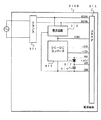
【0034】
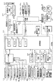
機構板36には、中継基板30を介して可変表示部9を制御する可変表示制御ユニット29、基板ケース32に覆われ遊技制御用マイクロコンピュータ等が搭載された遊技制御基板(主基板)31、可変表示制御ユニット29と遊技制御基板31との間の信号を中継するための中継基板33、および景品玉の払出制御を行う賞球制御用マイクロコンピュータ等が搭載された賞球制御基板37が設置されている。さらに、機構板36の下部には、モータの回転力を利用して打球を遊技領域7に発射する打球発射装置34と、遊技効果ランプ・LED28a,28b,28c、賞球ランプ51および球切れランプ52に信号を送るためのランプ制御基板35が設置されている。
【0035】
また、図3はパチンコ遊技機1の遊技盤を背面からみた背面図である。誘導樋39を通った玉は、図3に示されるように、球切れ検出器187a,187bを通過して玉供給樋186a,186bを経て玉払出装置97に至る。玉払出装置97から払い出された景品玉は、連絡口45を通ってパチンコ遊技機1の前面に設けられている打球供給皿3に供給される。連絡口45の側方には、パチンコ遊技機1の前面に設けられている余剰玉受皿4に連通する余剰玉通路46が形成されている。入賞にもとづく景品玉が多数払い出されて打球供給皿3が満杯になり、ついには景品玉が連絡口45に到達した後さらに景品玉が払い出されると景品玉は、余剰玉通路46を経て余剰玉受皿4に導かれる。さらに景品玉が払い出されると、感知レバー47が満タンスイッチ48を押圧して満タンスイッチ48がオンする。その状態では、玉払出装置97内のステッピングモータの回転が停止して玉払出装置97の動作が停止するとともに、必要に応じて打球発射装置34の駆動も停止する。なお、この実施の形態では、電気的駆動源の駆動によって遊技球を払い出す玉払出装置として、ステッピングモータの回転によって遊技球が払い出される玉払出装置97を例示するが、その他の駆動源によって遊技球を送り出す構造の玉払出装置を用いてもよいし、電気的駆動源の駆動によってストッパを外し遊技球の自重によって払い出しがなされる構造の玉払出装置を用いてもよい。
【0036】
賞球払出制御を行うために、入賞口スイッチ19a,24a、始動口スイッチ17およびVカウントスイッチ22からの信号が、主基板31に送られる。主基板31のCPU56は、始動口スイッチ17がオンすると6個の賞球払出に対応した入賞が発生したことを知る。また、カウントスイッチ23がオンすると15個の賞球払出に対応した入賞が発生したことを知る。そして、入賞口スイッチがオンすると10個の賞球払出に対応した入賞が発生したことを知る。なお、この実施の形態では、例えば、入賞口24に入賞した遊技球は、入賞口24からの入賞球流路に設けられている入賞口スイッチ24aで検出され、入賞口19に入賞した遊技球は、入賞口19からの入賞球流路に設けられている入賞口スイッチ19aで検出される。
【0037】
図4は、主基板31における回路構成の一例を示すブロック図である。なお、図4には、賞球制御基板37、ランプ制御基板35、音制御基板70、発射制御基板91および表示制御基板80も示されている。主基板31には、プログラムに従ってパチンコ遊技機1を制御する基本回路53と、ゲートスイッチ12、始動口スイッチ17、Vカウントスイッチ22、カウントスイッチ23および入賞口スイッチ19a,24aからの信号を基本回路53に与えるスイッチ回路58と、可変入賞球装置15を開閉するソレノイド16および開閉板20を開閉するソレノイド21を基本回路53からの指令に従って駆動するソレノイド回路59と、始動記憶表示器18の点灯および滅灯を行うとともに7セグメントLEDによる可変表示器10と装飾ランプ25とを駆動するランプ・LED回路60とが搭載されている。
【0038】
また、基本回路53から与えられるデータに従って、大当りの発生を示す大当り情報、可変表示部9の画像表示開始に利用された始動入賞球の個数を示す有効始動情報、確率変動が生じたことを示す確変情報等をホール管理コンピュータ等のホストコンピュータに対して出力する情報出力回路64を含む。
【0039】
基本回路53は、ゲーム制御用のプログラム等を記憶するROM54、ワークメモリとして使用される記憶手段の一例であるRAM55、制御用のプログラムに従って制御動作を行うCPU56およびI/Oポート部57を含む。この実施の形態では、ROM54,RAM55はCPU56に内蔵されている。すなわち、CPU56は、1チップマイクロコンピュータである。なお、1チップマイクロコンピュータは、少なくともRAM55が内蔵されていればよく、ROM54およびI/Oポート部57は外付けであっても内蔵されていてもよい。また、I/Oポート部57は、マイクロコンピュータにおける情報入出力可能な端子である。
【0040】
さらに、主基板31には、電源投入時に基本回路53をリセットするための初期リセット回路65と、基本回路53から与えられるアドレス信号をデコードしてI/Oポート部57のうちのいずれかのI/Oポートを選択するための信号を出力するアドレスデコード回路67とが設けられている。
なお、玉払出装置97から主基板31に入力されるスイッチ情報もあるが、図4ではそれらは省略されている。
【0041】
遊技球を打撃して発射する打球発射装置は発射制御基板91上の回路によって制御される駆動モータ94で駆動される。そして、駆動モータ94の駆動力は、操作ノブ5の操作量に従って調整される。すなわち、発射制御基板91上の回路によって、操作ノブ5の操作量に応じた速度で打球が発射されるように制御される。
【0042】
図5は、賞球制御基板37および玉払出装置97の構成要素などの賞球に関連する構成要素を示すブロック図である。図5に示すように、満タンスイッチ48からの検出信号は、中継基板71を介して主基板31のI/Oポート57に入力される。満タンスイッチ48は、余剰玉受皿4の満タンを検出するスイッチである。
【0043】
球切れ検出スイッチ167および球切れスイッチ187(187a,187b)からの検出信号は、中継基板72および中継基板71を介して主基板31のI/Oポート57に入力される。球切れ検出スイッチ167は景品玉タンク38内の補給玉の不足を検出するスイッチであり、球切れスイッチ187は、景品玉通路内の景品玉の有無を検出するスイッチである。
【0044】
主基板31のCPU56は、球切れ検出スイッチ167または球切れスイッチ187からの検出信号が球切れ状態を示しているか、または、満タンスイッチ48からの検出信号が満タン状態を示していると、玉貸し禁止を指示する賞球制御コマンドを送出する。玉貸し禁止を指示する賞球制御コマンドを受信すると、賞球制御基板37の賞球制御用CPU371は、玉貸し処理を停止する。
【0045】
さらに、賞球カウントスイッチ301Aおよび玉貸しカウントスイッチ301Bからの検出信号も、中継基板72および中継基板71を介して主基板31のI/Oポート57に入力される。また、賞球カウントスイッチ301Aおよび玉貸しカウントスイッチ301Bは、玉払出装置97の賞球機構部分に設けられ、実際に払い出された賞球を検出する。
【0046】
入賞があると、賞球制御基板37には、主基板31の出力ポート(ポートG,H)577,578から賞球個数を示す賞球制御コマンドが入力される。出力ポート577は8ビットのデータを出力し、出力ポート578は1ビットのストローブ信号(INT信号)を出力する。賞球個数を示す賞球制御コマンドは、入力バッファ回路373を介してI/Oポート372aに入力される。賞球制御用CPU371は、I/Oポート372aを介して賞球制御コマンドを入力し、賞球制御コマンドに応じて玉払出装置97を駆動して賞球払出を行う。なお、この実施の形態では、賞球制御用CPU371は、1チップマイクロコンピュータであり、少なくともRAMが内蔵されている。
【0047】
賞球制御用CPU371は、出力ポート372gを介して、貸し玉数を示す玉貸し個数信号をターミナル基板160に出力し、ブザー駆動信号をブザー基板75に出力する。ブザー基板75にはブザーが搭載されている。さらに、出力ポート372eを介して、エラー表示用LED374にエラー信号を出力する。
【0048】
さらに、賞球制御基板37の入力ポート372bには、中継基板72を介して、賞球カウントスイッチ301Aの検出信号の検出信号が入力される。賞球制御基板37からの払出モータ289への駆動信号は、出力ポート372cおよび中継基板72を介して玉払出装置97の賞球機構部分における払出モータ289に伝えられる。
【0049】
カードユニット50には、カードユニット制御用マイクロコンピュータが搭載されている。また、カードユニット50には、端数表示スイッチ152、連結台方向表示器153、カード投入表示ランプ154およびカード挿入口155が設けられている(図1参照)。残高表示基板74には、打球供給皿3の近傍に設けられている度数表示LED、玉貸しスイッチおよび返却スイッチが接続される。
【0050】
残高表示基板74からカードユニット50には、遊技者の操作に応じて、玉貸しスイッチ信号および返却スイッチ信号が賞球制御基板37を介して与えられる。また、カードユニット50から残高表示基板74には、プリペイドカードの残高を示すカード残高表示信号および玉貸し可表示信号が賞球制御基板37を介して与えられる。カードユニット50と賞球制御基板37の間では、ユニット操作信号(BRDY信号)、玉貸し要求信号(BRQ信号)、玉貸し完了信号(EXS信号)およびパチンコ機動作信号(PRDY信号)がI/Oポート372fを介してやりとりされる。
【0051】
パチンコ遊技機1の電源が投入されると、賞球制御基板37の賞球制御用CPU371は、カードユニット50にPRDY信号を出力する。カードユニット50においてカードが受け付けられ、玉貸しスイッチが操作され玉貸しスイッチ信号が入力されると、カードユニット制御用マイクロコンピュータは、賞球制御基板37にBRDY信号を出力する。この時点から所定の遅延時間が経過すると、カードユニット制御用マイクロコンピュータは、賞球制御基板37にBRQ信号を出力する。そして、賞球制御基板37の賞球制御用CPU371は、払出モータ289を駆動し、所定個の貸し玉を遊技者に払い出す。そして、払出が完了したら、賞球制御用CPU371は、カードユニット50にEXS信号を出力する。
【0052】
以上のように、カードユニット50からの信号は全て賞球制御基板37に入力される構成になっている。従って、玉貸し制御に関して、カードユニット50から主基板31に信号が入力されることはなく、主基板31の基本回路53にカードユニット50の側から不正に信号が入力される余地はない。なお、主基板31および賞球制御基板37には、ソレノイドおよびモータやランプを駆動するためのドライバ回路が搭載されているが、図5では、それらの回路は省略されている。
【0053】
なお、この実施の形態ではカードユニット50が設けられている場合を例にするが、コイン投入に応じてその金額に応じた遊技球を貸し出す場合にも本発明を適用できる。
【0054】
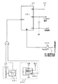
図6は、電源監視および電源バックアップのためのCPU56周りの一構成例を示すブロック図である。図6に示すように、電源基板に搭載されている第1の電源監視回路(第1の電源監視手段)からの電圧低下信号が、CPU56のマスク不能割込端子(NMI端子)に接続されている。第1の電源監視回路は、遊技機が使用する各種直流電源のうちのいずれかの電源の電圧を監視して電源電圧低下を検出する回路である。従って、CPU56は、割込処理によって電源断の発生を確認することができる。
【0055】
主基板31において、第1の電源監視手段からの電圧低下信号は、入力バッファ回路900を介してCPU56側に入力されている。ここでは、入力バッファ回路900として74HC244を例示するが、入力バッファ機能を有する回路であるならばどのような回路を用いてもよい。また、入力バッファ回路900は、電源基板側から主基板31の内部側への方向にのみ信号を通過させる不可逆性素子である。
【0056】
主基板31には、第2の電源監視回路903が搭載されている。この例では、第2の電源監視回路903において、電源監視用IC904が、第1の電源監視回路が監視する電源電圧と等しい電源電圧である+30V電源電圧を監視して電圧値が所定値以下になるとローレベルの電圧低下信号を発生する。そして、例えば、電源基板に搭載される第1の電源監視回路の検出電圧(電圧低下信号を出力することになる電圧)を+21Vとし、第2の電源監視回路903の検出電圧を+9Vとする。
【0057】
よって、この例では、第1の電源監視手段が検出信号を出力することになる第1検出条件は+30V電源電圧が+21Vにまで低下したことであり、第2の電源監視手段が検出信号を出力することになる第2検出条件は+30V電源電圧が+9Vにまで低下したことになる。ただし、ここで用いられている電圧値は一例であって、他の値を用いてもよい。
【0058】
そのように構成した場合には、同一の電圧を監視するので、第1の電圧監視回路が電圧低下信号を出力するタイミングと第2の電圧監視回路が電圧低下信号を出力するタイミングの差を所望の所定期間に確実に設定することができる。所望の所定期間とは、第1の電源監視回路からの電圧低下信号に応じて電力供給停止時処理を開始してから電力供給停止時処理が確実に完了するまでの期間である。
【0059】
第2の電源監視回路903からの電圧低下信号は、初期リセット回路65からの初期リセット信号と論理和をとられた後に、CPU56のリセット端子に入力される。従って、CPU56は、初期リセット回路65からの初期リセット信号がローレベルを呈しているとき、または、第2の電源監視回路903からの電圧低下信号がローレベルを呈しているときに、リセット状態(非動作状態)になる。
【0060】
なお、初期リセット回路65のリセットIC651は、遊技機に電源が投入され+5V電源の電圧が上昇していくときに、+5V電源電圧が所定値以上になると、出力信号をハイレベルにする。すなわち、初期リセット信号をオフ状態にする。
【0061】
CPU56等の駆動電源である+5V電源から電力が供給されていない間、RAMの少なくとも一部は、電源基板から供給されるバックアップ電源によってバックアップされ、遊技機に対する電源が断しても内容は保存される。そして、+5V電源が復旧すると、初期リセット回路65からリセット信号が発せられるので、CPU56は、通常の動作状態に復帰する。そのとき、必要なデータがバックアップされているので、停電等からの復旧時には停電発生時の遊技状態に復帰することができる。
【0062】
図7は、遊技機の電源基板910の一構成例を示すブロック図である。電源基板910は、主基板31、表示制御基板80、音制御基板70、ランプ制御基板35および賞球制御基板37等の電気部品制御基板と独立して設置され、遊技機内の各電気部品制御基板および機構部品が使用する電圧を生成する。この例では、AC24V、DC+30V、DC+21V、DC+12VおよびDC+5Vを生成する。また、バックアップ電源となるコンデンサ916は、DC+5Vすなわち各基板上のIC等を駆動する電源のラインから充電される。
【0063】
トランス911は、交流電源からの交流電圧を24Vに変換する。AC24V電圧は、コネクタ915に出力される。また、整流回路912は、AC24Vから+30Vの直流電圧を生成し、DC−DCコンバータ913およびコネクタ915に出力する。DC−DCコンバータ913は、+21V、+12Vおよび+5Vを生成してコネクタ915に出力する。コネクタ915は例えば中継基板に接続され、中継基板から各電気部品制御基板および機構部品に必要な電圧の電力が供給される。なお、トランス911の入力側には、遊技機に対する電源供給を停止したり開始させたりするための電源スイッチ918が設置されている。
【0064】
DC−DCコンバータ913からの+5Vラインは分岐してバックアップ+5Vラインを形成する。バックアップ+5Vラインとグラウンドレベルとの間には大容量のコンデンサ916が接続されている。コンデンサ916は、遊技機に対する電力供給が遮断されたときの電気部品制御基板のバックアップRAM(電源バックアップされているRAMすなわち記憶内容保持状態となりうる記憶手段)に対して記憶状態を保持できるように電力を供給するバックアップ電源となる。また、+5Vラインとバックアップ+5Vラインとの間に、逆流防止用のダイオード917が挿入される。
【0065】
なお、バックアップ電源として、+5V電源から充電可能な電池を用いてもよい。電池を用いる場合には、+5V電源から電力供給されない状態が所定時間継続すると容量がなくなるような充電池が用いられる。
【0066】
また、電源基板910には、上述した第1の電源回路を構成する電源監視用IC902が搭載されている。電源監視用IC902は、+30V電源電圧を導入し、+30V電源電圧を監視することによって電源断の発生を検出する。具体的には、+30V電源電圧が所定値(この例では+21V)以下になったら、電源断が生ずるとして電圧低下信号を出力する。なお、監視対象の電源電圧は、各電気部品制御基板に搭載されている回路素子の電源電圧(この例では+5V)よりも高い電圧であることが好ましい。この例では、交流から直流に変換された直後の電圧である+30Vが用いられている。電源監視用IC902からの電圧低下信号は、主基板31や賞球制御基板37等に供給される。
【0067】
電源監視用IC902が電源断を検知するための所定値は、通常時の電圧より低いが、各電気部品制御基板上のCPUが暫くの間動作しうる程度の電圧である。また、電源監視用IC902が、CPU等の回路素子を駆動するための電圧(この例では+5V)よりも高く、また、交流から直流に変換された直後の電圧を監視するように構成されているので、CPUが必要とする電圧に対して監視範囲を広げることができる。従って、より精密な監視を行うことができる。さらに、監視電圧として+30Vを用いる場合には、遊技機の各種スイッチに供給される電圧が+12Vであることから、電源瞬断時のスイッチオン誤検出の防止も期待できる。すなわち、+30V電源の電圧を監視すると、+30V作成の以降に作られる+12Vが落ち始める以前の段階でそれの低下を検出できる。よって、+12V電源の電圧が低下するとスイッチ出力がオン状態を呈するようになるが、+12Vより早く低下する+30V電源電圧を監視して電源断を認識すれば、スイッチ出力がオン状態を呈する前に電源復旧待ちの状態に入ってスイッチ出力を検出しない状態となることができる。
【0068】
また、電源監視用IC902は、電気部品制御基板とは別個の電源基板910に搭載されているので、第1の電源監視回路から複数の電気部品制御基板に電圧低下信号を供給することができる。電圧低下信号を必要とする電気部品制御基板が幾つあっても第1の電源監視手段は1つ設けられていればよいので、各電気部品制御基板における各電気部品制御手段が後述する電源復帰制御を行っても、遊技機のコストはさほど上昇しない。
【0069】
なお、図7に示された構成では、電源監視用IC902の検出出力(電圧低下信号)は、バッファ回路918,919を介してそれぞれの電気部品制御基板に伝達されるが、例えば、1つの検出出力を中継基板に伝達し、中継基板から各電気部品制御基板に同じ信号を分配する構成でもよい。
【0070】
次に遊技機の動作について説明する。
図8は、主基板31におけるCPU56が実行するメイン処理を示すフローチャートである。遊技機に対する電源が投入されると、メイン処理において、CPU56は、まず、停電からの復旧時であったか否か確認する(ステップS1)。停電からの復旧時であったか否かは、例えば、電源断時にバックアップRAM領域に設定される電源断フラグによって確認される。
【0071】
停電からの復旧時であった場合には、バックアップRAM領域のデータチェック(この例ではパリティチェック)を行う(ステップS3)。不測の電源断が生じた後に復旧した場合には、バックアップRAM領域のデータは保存されていたはずであるから、チェック結果は正常になる。チェック結果が正常でない場合には、内部状態を電源断時の状態に戻すことができないので、停電復旧時でない電源投入時に実行される初期化処理を実行する(ステップS4,S2)。
【0072】
チェック結果が正常であれば、CPU56は、内部状態を電源断時の状態に戻すための遊技状態復旧処理を行うとともに(ステップS5)、電源断フラグをクリアする(ステップS6)。
【0073】
停電からの復旧時でない場合には、CPU56は、通常の初期化処理を実行する(ステップS1,S2)。その後、メイン処理では、タイマ割込フラグの監視(ステップS6)の確認が行われるループ処理に移行する。なお、ループ内では、表示用乱数更新処理(ステップS7)も実行される。
【0074】
なお、ここでは、ステップS1で停電からの復旧か否かを確認し、停電からの復旧時であればパリティチェックを行ったが、最初に、パリティチェックを実行し、チェック結果が正常でなければ停電からの復旧ではないと判断してステップS2の初期化処理を実行し、チェック結果が正常であれば遊技状態復帰処理を行ってもよい。すなわち、パリティチェックの結果をもって停電からの復旧であるか否かを判断してもよい。
【0075】
また、停電復旧処理を実行するか否か判断する場合に、すなわち、遊技状態を復旧するか否か判断する際に、保存されていたRAMデータにおける特別プロセスフラグ等や始動入賞記憶数データによって、遊技機が遊技待機状態(図柄変動中でなく、大当り遊技中でなく、確変中でなく、また、始動入賞記憶がない状態)であることが確認されたら、遊技状態復旧処理を行わずに初期化処理を実行するようにしてもよい。
【0076】
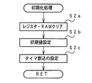
通常の初期化処理では、図9に示すように、レジスタおよびRAMのクリア処理(ステップS2a)と、必要な初期値設定処理(ステップS2b)が行われた後に、2ms毎に定期的にタイマ割込がかかるようにCPU56に設けられているタイマレジスタの初期設定(タイムアウトが2msであることと繰り返しタイマが動作する設定)が行われる(ステップS2c)。すなわち、ステップS2cで、タイマ割込を能動化する処理と、タイマ割込インタバルを設定する処理とが実行される。
【0077】
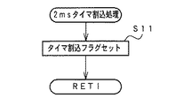
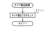
従って、この実施の形態では、CPU56の内部タイマが繰り返しタイマ割込を発生するように設定される。この実施の形態では、繰り返し周期は2msに設定される。そして、図10に示すように、タイマ割込が発生すると、CPU56は、タイマ割込フラグをセットする(ステップS11)。
【0078】
CPU56は、ステップS8において、タイマ割込フラグがセットされたことを検出すると、タイマ割込フラグをリセットするとともに(ステップS9)、遊技制御処理を実行する(ステップS10)。以上の制御によって、この実施の形態では、遊技制御処理は2ms毎に起動されることになる。なお、この実施の形態では、タイマ割込処理ではフラグセットのみがなされ、遊技制御処理はメイン処理において実行されるが、タイマ割込処理で遊技制御処理を実行してもよい。
【0079】
図11は、ステップS10の遊技制御処理を示すフローチャートである。遊技制御処理において、CPU56は、まず、表示制御基板80に送出される表示制御コマンドをRAM55の所定の領域に設定する処理を行った後に(表示制御データ設定処理:ステップS21)、表示制御コマンドを出力する処理を行う(表示制御データ出力処理:ステップS22)。
【0080】
次いで、各種出力データの格納領域の内容を各出力ポートに出力する処理を行う(データ出力処理:ステップS23)。また、ホール管理用コンピュータに出力される大当り情報、始動情報、確率変動情報などの出力データを格納領域に設定する出力データ設定処理を行う(ステップS24)。さらに、パチンコ遊技機1の内部に備えられている自己診断機能によって種々の異常診断処理が行われ、その結果に応じて必要ならば警報が発せられる(エラー処理:ステップS25)。
【0081】
次に、遊技制御に用いられる大当り判定用の乱数等の各判定用乱数を示す各カウンタを更新する処理を行う(ステップS26)。
【0082】
さらに、CPU56は、特別図柄プロセス処理を行う(ステップS27)。特別図柄プロセス制御では、遊技状態に応じてパチンコ遊技機1を所定の順序で制御するための特別図柄プロセスフラグに従って該当する処理が選び出されて実行される。そして、特別図柄プロセスフラグの値は、遊技状態に応じて各処理中に更新される。また、普通図柄プロセス処理を行う(ステップS28)。普通図柄プロセス処理では、7セグメントLEDによる可変表示器10を所定の順序で制御するための普通図柄プロセスフラグに従って該当する処理が選び出されて実行される。そして、普通図柄プロセスフラグの値は、遊技状態に応じて各処理中に更新される。
【0083】
さらに、CPU56は、スイッチ回路58を介して、ゲートセンサ12、始動口センサ17、カウントセンサ23および入賞口スイッチ19a,24aの状態を入力し、各入賞口や入賞装置に対する入賞があったか否か判定する(スイッチ処理:ステップS29)。CPU56は、さらに、停止図柄の種類を決定する乱数等の表示用乱数を更新する処理を行う(ステップS30)。
【0084】
また、CPU56は、賞球制御基板37との間の信号処理を行う(ステップS31)。すなわち、所定の条件が成立すると賞球制御基板37に賞球制御コマンドを出力する。賞球制御基板37に搭載されている賞球制御用CPUは、賞球制御コマンドに応じて玉払出装置97を駆動する。
【0085】
以上のように、メイン処理には遊技制御処理に移行すべきか否かを判定する処理が含まれ、CPU56の内部タイマが定期的に発生するタイマ割込にもとづくタイマ割込処理で遊技制御処理に移行すべきか否かを判定するためのフラグがセットされるので、遊技制御処理の全てが確実に実行される。つまり、遊技制御処理の全てが実行されるまでは、次回の遊技制御処理に移行すべきか否かの判定が行われないので、遊技制御処理中の全ての各処理が実行完了することは保証されている。
【0086】
従来の一般的な遊技制御処理は、定期的に発生する外部割込によって、強制的に最初の状態に戻されていた。図11に示された例に則して説明すると、例えば、ステップS31の処理中であっても、強制的にステップS21の処理に戻されていた。つまり、遊技制御処理中の全ての各処理が実行完了する前に、次回の遊技制御処理が開始されてしまう可能性があった。
【0087】
なお、ここでは、主基板31のCPU56が実行する遊技制御処理は、CPU56の内部タイマが定期的に発生するタイマ割込にもとづくタイマ割込処理でセットされるフラグに応じて実行されたが、定期的に(例えば2ms毎)信号を発生するハードウェア回路を設け、その回路からの信号をCPU56の外部割込端子に導入し、割込信号によって遊技制御処理に移行すべきか否かを判定するためのフラグをセットするようにしてもよい。
【0088】
そのように構成した場合にも、遊技制御処理の全てが実行されるまでは、フラグの判定が行われないので、遊技制御処理中の全ての各処理が実行完了することが保証される。
【0089】
図12は、電源基板910の第1の電源監視回路からの電圧低下信号にもとづくNMIに応じて実行される停電発生NMI処理の一例を示すフローチャートである。停電発生NMI処理において、CPU56は、まず、割込禁止に設定する(ステップS41)。停電発生NMI処理ではRAM内容の保存を確実にするためにチェックサムの生成処理を行う。その処理中に他の割込処理が行われたのではチェックサムの生成処理が完了しないうちにCPUが動作し得ない電圧にまで低下してしまうことがことも考えられるので、まず、他の割込が生じないような設定がなされる。なお、停電発生NMI処理におけるステップS43〜S49は、電力供給停止時処理の一例である。
【0090】
なお、割込処理中では他の割込がかからないような仕様のCPUを用いている場合には、ステップS41の処理は不要である。
【0091】
次いで、CPU56は、電源断フラグが既にセットされているか否か確認する(ステップS42)。電源断フラグが既にセットされていれば、以後の処理を行わない。電源断フラグがセットされていなければ、以下の電力供給停止時処理を実行する。すなわち、ステップS43からステップS49の処理を実行する。
【0092】
まず、全ての出力ポートをオフ状態にする(ステップS43)。そして、必要ならば各レジスタの内容をバックアップRAM領域に格納する(ステップS44)。さらに、バックアップRAM領域のバックアップチェックデータ領域に適当な初期値を設定し(ステップS45)、初期値およびバックアップRAM領域のデータについて順次排他的論理和をとって(ステップS46)、最終的な演算値をバックアップパリティデータ領域に設定する(ステップS47)。その後、電源断フラグをセットする(ステップS48)。また、RAMアクセス禁止状態にする(ステップS49)。電源電圧が低下していくときには、各種信号線のレベルが不安定になってRAM内容が化ける可能性があるが、このようにRAMアクセス禁止状態にしておけば、バックアップRAM内のデータが化けることはない。
【0093】
次いで、CPU56は、ループ処理にはいる。すなわち、何らの処理もしない状態になる。従って、図6に示された電源監視用IC904からのリセット信号によって外部から動作禁止状態にされる前に、内部的に動作停止状態になる。よって、電源断時に確実にCPU56は動作停止する。その結果、上述したRAMアクセス禁止の制御および動作停止制御によって、電源電圧が低下していくことに伴って生ずる可能性がある異常動作に起因するRAMの内容破壊等を確実に防止することができる。
【0094】
なお、この実施の形態では、停電発生NMI処理では最終部でプログラムをループ状態にしたが、ホールト(HALT)命令を発行するように構成してもよい。
【0095】
また、RAMアクセス禁止にする前にセットされる電源断フラグは、上述したように、電源投入時において停電からの復旧か否かを判断する際に使用される。また、ステップS41からS49の処理は、第2の電源監視手段が電圧低下信号を発生する前に完了する。換言すれば、第2の電源監視手段が電圧低下信号を発生する前に完了するように、第1の電圧監視手段および第2の電圧監視手段の検出電圧の設定が行われている。
【0096】
この実施の形態では、電力供給停止時処理開始時に、電源断フラグの確認が行われる。そして、電源断フラグが既にセットされている場合には電力供給停止時処理を実行しない。上述したように、電源断フラグは、電力供給停止時処理が完了したことを示すフラグである。従って、例えば、リセット待ちのループ状態で何らかの原因で再度NMIが発生したとしても、電力供給停止時処理が重複して実行されてしまうようなことはない。
【0097】
ただし、割込処理中では他の割込がかからないような仕様のCPUを用いている場合には、ステップS42の判断は不要である。
【0098】
図13は、バックアップパリティデータ作成方法を説明するための説明図である。ただし、図13に示す例では、簡単のために、バックアップデータRAM領域のデータのサイズを3バイトとする。電源電圧低下にもとづく停電発生処理において、図13(A)に示すように、バックアップチェックデータ領域に、初期データ(この例では00H)が設定される。次に、「00H」と「F0H」の排他的論理和がとられ、その結果と「16H」の排他的論理和がとられる。さらに、その結果と「DFH」の排他的論理和がとられる。そして、その結果(この例では「39H」)がバックアップパリティデータ領域に設定される。
【0099】
電源が再投入されたときには、停電復旧処理においてパリティ診断が行われるが、図13(B)はパリティ診断の例を示す説明図である。バックアップ領域の全データがそのまま保存されていれば、電源再投入時に、図13(A)に示すようなデータがバックアップ領域に設定されている。
【0100】
ステップS51の処理において、CPU56は、バックアップRAM領域のバックアップパリティデータ領域に設定されていたデータ(この例では「39H」)を初期データとして、バックアップデータ領域の各データについて順次排他的論理和をとる処理を行う。バックアップ領域の全データがそのまま保存されていれば、最終的な演算結果は、「00H」、すなわちバックアップチェックデータ領域に設定されているデータと一致する。バックアップRAM領域内のデータにビット誤りが生じていた場合には、最終的な演算結果は「00H」にならない。
【0101】
よって、CPU56は、最終的な演算結果とバックアップチェックデータ領域に設定されているデータとを比較して、一致すればパリティ診断正常とする。一致しなければ、パリティ診断異常とする。
【0102】
以上のように、この実施の形態では、遊技制御手段には、遊技機の電源が断しても、所定期間電源バックアップされる記憶手段(この例ではバックアップRAM)が設けられ、電源投入時に、CPU56(具体的にはCPU56が実行するプログラム)は、記憶手段がバックアップ状態にあればバックアップデータにもとづいて遊技状態を回復させる遊技状態復旧処理(ステップS5)を行うように構成される。
【0103】
この実施の形態では、図7に示されたように電源基板910に第1の電源監視手段が搭載され、図6に示されたように主基板31に第2の電源監視手段が搭載されている。そして、電源電圧が低下していくときに、第2の電源監視手段(この例では電源監視用IC904)が電圧低下信号を発生する時期は、第1の電源監視手段(この例では電源監視用IC902)が電圧低下信号を発生する時期よりも遅くなるように設定されている。さらに、第2の電源監視手段からの電圧低下信号は、CPU56のリセット端子に入力されている。
【0104】
すると、CPU56は、第1の電源監視手段(電源監視用IC902)からの電圧低下信号にもとづいて停電発生処理(電力供給停止時処理)を実行した後にループ状態に入るのであるが、ループ状態において、リセット状態に入ることになる。すなわち、CPU56の動作が完全に停止する。ループ状態においては+5V電源電圧値が徐々に低下するので入出力状態が不定になるが、CPU56はリセット状態になるので、不定データにもとづいて異常動作してしまうことは防止される。
【0105】
このように、この実施の形態では、CPU56が、第1の電源監視手段からの検出出力の入力に応じてループ状態に入るとともに、第2の電源監視手段からの検出出力の入力に応じてシステムリセットされるように構成したので、電源断時に確実なデータ保存を行うことができ、遊技者に不利益がもたらされることを防止することができる。
【0106】
なお、この実施の形態では、電源監視用IC902,904は、同一の電源電圧を監視しているが、異なる電源電圧を監視してもよい。例えば、電源基板910の第1の電源監視回路が+30V電源電圧を監視し、主基板31の第2の電源監視回路が+5V電源電圧を監視してもよい。そして、第2の電源監視回路がローレベルの電圧低下信号を発生するタイミングは第1の電源監視回路が電圧低下信号を発生するタイミングに対して遅くなるように、主基板31の電源監視用IC904のしきい値レベル(電圧低下信号を発生する電圧レベル)が設定される。例えば、しきい値は4.25Vである。4.25Vは、通常時の電圧より低いが、CPU56が暫くの間動作しうる程度の電圧である。
【0107】
また、上記の実施の形態では、CPU56は、マスク不能割込端子(NMI端子)を介して電源基板からの第1の電圧低下信号(第1の電源監視手段からの電圧低下信号)を検知したが、第1の電圧低下信号をマスク可能割込割込端子(IRQ端子)に導入してもよい。その場合には、割込処理(IRQ処理)で電力供給停止時処理が実行される。また、入力ポートを介して電源基板からの第1の電圧低下信号を検知してもよい。その場合には、メイン処理において入力ポートの監視が行われる。
【0108】
また、IRQ端子を介して電源基板からの第1の電圧低下信号を検知する場合に、メイン処理のステップS10の遊技制御処理の開始時にIRQ割込マスクをセットし、遊技制御処理の終了時にIRQ割込マスクを解除するようにしてもよい。そのようにすれば、遊技制御処理の開始前および終了後に割込がかかることになって、遊技制御処理が中途で中断されることはない。従って、賞球制御コマンドを賞球制御基板37に送出しているときなどにコマンド送出が中断されてしまうようなことはない。よって、停電が発生するようなときでも、賞球制御コマンド等は確実に送出完了する。
【0109】
以下、遊技状態復旧処理について説明する。
まず、この実施の形態において、主基板31のCPU56が、表示制御基板80、音制御基板70およびランプ制御基板35に送出する表示制御コマンド、音制御コマンドおよびランプ制御コマンドについて説明する。各制御コマンドは、図11に示された遊技制御処理における特別図柄プロセス処理(ステップS27)で遊技進行に応じて送出することが決定され、表示制御データ設定処理(ステップS21)で具体的なデータが設定され、表示制御データ出力処理(ステップS22)で出力ポートから出力されることによって送出される。
【0110】
図14(A)は、可変表示部9における図柄変動に関する各制御コマンドの送出タイミング例を示す説明図である。この実施の形態では、主基板31のCPU56は、図柄変動を開始させるときに、表示制御基板80、音制御基板70およびランプ制御基板35のそれぞれに対して変動開始コマンドを送出する。表示制御基板80に対しては、さらに、左右中図柄の確定図柄を示す図柄指定コマンドを送出する。
【0111】
そして、図柄変動を確定させるときに、表示制御基板80、音制御基板70およびランプ制御基板35のそれぞれに対して変動停止コマンドを送出する。表示制御基板80、音制御基板70およびランプ制御基板35に搭載されている各CPUは、変動開始コマンドで指定された変動態様に応じた表示制御、音発生制御およびランプ点灯制御を行う。なお、変動開始コマンドには変動時間を示す情報が含まれている。
【0112】
図14(B)は、可変表示部9の表示結果が所定の大当り図柄であった場合に実行される大当り遊技に関する各制御コマンドの送出タイミング例を示す説明図である。この実施の形態では、主基板31のCPU56は、大当り遊技開始時に、表示制御基板80、音制御基板70およびランプ制御基板35のそれぞれに対して大当り開始コマンドを送出する。また、所定時間経過後に、1ラウンド(1R)指定コマンドを送出する。表示制御基板80、音制御基板70およびランプ制御基板35に搭載されている各CPUは、大当り開始コマンドを受信すると、大当り開始時の表示制御、音発生制御およびランプ点灯制御を行う。また、1ラウンド指定コマンドを受信すると、大当り中の表示制御、音発生制御およびランプ点灯制御を行う。ただし、表示制御基板80のCPUは、1ラウンド目の表示を行う。
【0113】
その後、主基板31のCPU56は、表示制御基板80に対して各ラウンドを示すコマンド等を順次送出する。表示制御基板80のCPUは、それらのコマンドに応じて対応する表示制御を行う。
【0114】
また、大当り遊技終了時に、主基板31のCPU56は、表示制御基板80、音制御基板70およびランプ制御基板35のそれぞれに対して大当り終了コマンドを送出する。そして、所定時間経過後に、通常画面表示コマンドを送出する。各電気部品制御手段は、通常画面表示コマンドを受信すると、制御状態を遊技待ちの状態にする。
【0115】
図15は、図12に示された停電復旧処理で行われる遊技状態復旧処理の一例を示すフローチャートである。この例では、CPU56は、レジスタ内容を復元する必要があれば、バックアップRAMに保存されていた値をレジスタに復元する(ステップS61)。そして、バックアップRAMに保存されていたデータにもとづいて停電時の遊技状態を確認する。例えば、特別図柄プロセス処理の進行状況に対応した特別図柄プロセスフラグの値によって遊技状態を確認することができる。
【0116】
遊技状態が図柄変動中であった場合には(ステップS62)、変動開始コマンドを表示制御基板80、音制御基板70およびランプ制御基板35に送出する制御を行う(ステップS63)。また、遊技状態が大当り遊技中であった場合には(ステップS64)、停電前に最後の送出された制御コマンドを表示制御基板80、音制御基板70およびランプ制御基板35に送出する制御を行う(ステップS65)。そして、それ以外の遊技状態であった場合には、例えば、通常画面表示コマンドを制御コマンドを表示制御基板80、音制御基板70およびランプ制御基板35に送出する制御を行う(ステップS66)。また、例えば、大当り中であった場合の可変入賞球装置15の状態復帰は、RAMのデータが保存されているため、後の遊技制御処理内で自動的に行われる。
【0117】
なお、ここでは、遊技状態復旧処理が終了するとメイン処理にリターンするように遊技状態復旧処理プログラムが構成されているが、電力供給停止時処理において保存されているスタックポインタが指すスタックエリア(バックアップRAM領域にある)に記憶されているアドレス(電源断時のNMI割込発生時に実行されていたアドレス)に戻るようにしてもよい。
【0118】
図16は、停電が発生した後に復旧した場合の制御状態の一例を示す説明図である。図16において、可変表示の状態は表示制御基板80のCPU(表示制御手段)によって実現され、音の状態は音制御基板70のCPU(音制御手段)によって実現され、ランプの状態はランプ制御基板35のCPU(ランプ制御手段)によって実現される。
【0119】
図16(A)は、図柄変動中に停電が生じた後に復旧した場合の例を示す。この場合には、電源復旧時に、主基板31から変動開始コマンドが送出される(図16におけるステップS63)。変動開始コマンドは、図柄変動開始時に送出されるコマンドであるから、可変表示制御、音制御およびランプ制御の状態は、変動開始時の状態に戻る。この実施の形態では、変動開始コマンドには変動時間を指定する情報を含まれ、主基板31のCPU56は変動開始コマンド送出後では変動終了時の確定コマンド(変動停止コマンド)まで何も送出しない(図柄指定コマンドを除く)。従って、図柄変動中に停電が生じた場合には、変動途中の状態から変動を再開することはできないが、変動開始コマンドを再送出することによって、表示制御、音制御およびランプ制御は同期した状態に戻る。
【0120】
なお、主基板31において、変動開始時に使用した各種パラメータはバックアップRAMに保存されている。従って、電源復旧後の変動における表示結果(確定図柄)等は、停電によって中断した変動においてなされるはずであった表示結果等と同じである。従って、遊技者に不利益が与えられるということはない。
【0121】
図16(B)は、大当り遊技中に停電が生じた後に復旧した場合の例を示す。この場合には、電源復旧時に、主基板31から停電前の最後に表示制御基板80、音制御基板70およびランプ制御基板35に送出されたコマンドが再送出される(図15におけるステップS65)。従って、音制御およびランプ制御は、大当り遊技中の制御状態に戻る。また、表示制御も、停電時に行われていた状態に戻る。
【0122】
なお、主基板31において、大当り遊技中の各種パラメータ(大入賞口開放回数、大入賞口入賞球数等)はバックアップRAMに保存されている。従って、遊技者にとっての遊技状態も停電前の状態に戻るので、遊技者に不利益が与えられるということはない。
【0123】
なお、上記の実施の形態では、遊技制御手段において、データ保存処理および復旧処理が行われる場合について説明したが、賞球制御手段、音声制御手段、ランプ制御手段および表示制御手段におけるRAMの一部も電源バックアップされ、賞球制御手段、表示制御手段、音制御手段およびランプ制御手段も、上述したような処理を行ってもよい。ただし、賞球制御手段、表示制御手段、音制御手段およびランプ制御手段は、復旧時にコマンド送出処理を行う必要はない。
【0124】
この実施の形態では、停電発生処理(電力供給停止時処理)において、電力供給停止時処理が既に実行されたことを示す電源断時フラグがセットされている場合には電力供給停止時処理を実行しないように構成されている。電源が断する過程では一般に電源電圧が不安定になるので、再度NMIが発生する可能性がある。すると、停電発生処理において電源断時フラグの確認を行わない場合には、再度発生したNMIによって再度電力供給停止時処理が実行される。
【0125】
最初に実行された正規の電力供給停止時処理では、例えばレジスタの内容をバックアップRAMに格納する処理が行われる(図12におけるステップS44参照)。最初に実行された正規の電力供給停止時処理後のリセット待ちの状態では電源電圧は徐々に低下していくので、レジスタの内容が破壊される可能性もある。すなわち、レジスタ値は、電源断が検出されたときの状態(最初にNMIが発生したとき)から変化している可能性がある。そのような状態で再度電力供給停止時処理が実行されると、電源断が検出されたときの状態のレジスタ値とは異なる値がバックアップRAMに格納されてしまう。すると、電源復旧時に実行される停電復旧処理において、電源断が検出されたときの状態のレジスタ値とは異なる値がレジスタに復旧されてしまう。その結果、電源断時の遊技状態とは異なる遊技状態が再現されてしまう可能性が生ずる。
【0126】
次に、賞球制御手段の停電発生時の動作について説明する。
図17は、電源監視および電源バックアップのための賞球制御用CPU371周りの一構成例を示すブロック図である。図17に示すように、電源基板910に搭載されている第1の電源監視回路(第1の電源監視手段)からの電圧低下信号が、賞球制御用CPU371のマスク不能割込端子(NMI端子)に入力されている。従って、賞球制御用CPU371は、NMI処理によって電源断の発生を確認することができる。
【0127】
賞球制御用CPU371等の駆動電源である+5V電源から電力が供給されていない間、賞球制御用CPU371の内蔵RAMの少なくとも一部は、電源基板910から供給されるバックアップ電源がバックアップ端子に接続されることによってバックアップされ、遊技機に対する電源が断しても内容は保存される。そして、+5V電源が復旧すると、初期リセット回路935からリセット信号が発せられるので、賞球制御用CPU371は、通常の動作状態に復帰する。そのとき、必要なデータがバックアップされているので、停電等からの復旧時には停電発生時の状態から払出制御を再開することができる。
【0128】
賞球制御基板37において、第1の電源監視手段からの電圧低下信号は、入力バッファ回路930を介して賞球制御CPU371側に入力されている。ここでは、入力バッファ回路930として74HC244を例示するが、入力バッファ機能を有する回路であるならばどのような回路を用いてもよい。また、入力バッファ回路930は、電源基板側から賞球制御基板37の内部側への方向にのみ信号を通過させる不可逆性素子である。
【0129】
図17に示す構成では、賞球制御基板37には、第2の電源監視回路933が搭載されている。この例では、第2の電源監視回路933において、電源監視用IC934が、電源基板910の第1の電源監視回路が監視する電源電圧と等しい電圧である+30V電源電圧を監視して電圧値が所定値以下になるとローレベルの電圧低下信号を発生する。第2の電源監視回路933が設けられている場合には、第2の電源監視回路933の検出電圧(電圧低下信号を出力することになる電圧)を、電源基板910に搭載されている第1の電源監視回路の検出電圧よりも低くする。
【0130】
第2の電源監視回路933からの電圧低下信号は、初期リセット回路935からの初期リセット信号と論理和をとられた後に、賞球制御用CPU371のリセット端子に入力される。従って、賞球制御用CPU371は、初期リセット回路935からの初期リセット信号がローレベルを呈しているとき、または、第2の電源監視回路933からの電圧低下信号がローレベルを呈しているときに、リセット状態(非動作状態)になる。
【0131】
図18は、主基板31から賞球制御基板37に送信される賞球制御コマンドのビット構成の一例を示す説明図である。図18に示すように、1バイト中の上位4ビットが制御指定部として使用され、下位4ビットが賞球数を示す領域として用いられる。
【0132】
図19に示すように、制御指定部において、ビット7,6,5,4が「0,1,0,0」であれば払出個数指定コマンドであることを示し、「0,1,0,1」であれば払出指定コマンドであることを示す。払出個数指定コマンドは、主基板31のCPU56が入賞を検出すると直ちに賞球制御基板37に送出される。
【0133】
ビット7,6,5,4が「1,0,0,0」である球切れ指定コマンドは、補給玉がなくなったことが検出されたときに主基板31から送信される。また、ビット7,6,5,4が「1,0,0,1」である発射停止指定コマンドは、余剰玉受皿4が満タンになって満タンスイッチ48がオンしたとき(満タン状態フラグがオンしたとき)に主基板31から送信される。
【0134】
賞球制御コマンドは、主基板31から賞球制御基板37に、1バイト(8ビット:賞球制御コマンドD7〜D0)のデータとして出力される。賞球制御コマンドD7〜D0は正論理で出力される。また、賞球制御コマンドD7〜D0が出力されたときには、負論理の賞球制御INT信号が出力される。
【0135】
この実施の形態では、図20に示すように、主基板31から賞球制御コマンドD7〜D0が出力されるときに、賞球制御INT信号が5μs以上ローレベルになる。賞球制御INT信号は、賞球制御基板37において、賞球制御用CPU371の割込端子に接続されている。よって、賞球制御用CPU371は、割り込みがあると、賞球制御コマンドD7〜D0が主基板31から送出されたことを認識でき、割込処理において賞球制御コマンド受信処理を行う。
【0136】
なお、図18に示されたコマンド構成は一例であって、他の構成にしてもよい。例えば、1バイト中の上位下位を、図18に示された構成とは逆にしてもよい。また、コマンド構成は1バイト構成でなく複数バイト構成であってもよい。
【0137】
図21は、賞球制御用CPU371のメイン処理を示すフローチャートである。メイン処理では、賞球制御用CPU371は、まず、RAM領域をクリアする等の初期値設定処理を行う(ステップS701)。なお、内蔵RAMの電源バックアップされたRAM領域(バックアップRAM領域)にデータが設定されている場合には、それらの領域のクリア処理はなされない。その後、この実施の形態では、賞球制御用CPU371は、タイマ割込フラグの監視(ステップS702)の確認を行うループ処理に移行する。
【0138】
ステップS701の初期化処理では、後述する総合個数記憶の値が0でない場合には、非バックアップRAM領域をクリアする。そして、賞球再開のための設定を行う。例えば、賞球中処理中フラグのセット等を行う。なお、バックアップRAM領域であっても、賞球個数に関わらない領域であるならば、それらのアドレスを指定してクリアするようにしてもよい。さらに、それら処理の他に、2ms毎に定期的にタイマ割込がかかるように賞球制御用CPU371に設けられているタイマレジスタの初期設定(タイムアウトが2msであることと繰り返しタイマが動作する設定)が行われる。すなわち、タイマ割込を能動化する処理と、タイマ割込インタバルを設定する処理とが実行される。
【0139】
従って、この実施の形態では、賞球制御用CPU371の内部タイマが繰り返しタイマ割込を発生するように設定される。この実施の形態では、繰り返し周期は2msに設定される。そして、図22に示すように、タイマ割込が発生すると、賞球制御用CPU371は、タイマ割込フラグをセットする(ステップS711)。
【0140】
賞球制御用CPU371は、ステップS702において、タイマ割込フラグがセットされたことを検出すると、タイマ割込フラグをリセットするとともに(ステップS703)、賞球制御処理および玉貸し制御処理を実行する(ステップS705,S706)。以上の制御によって、この実施の形態では、賞球制御処理および玉貸し制御処理は2ms毎に起動されることになる。なお、この実施の形態では、タイマ割込処理ではフラグセットのみがなされ、賞球制御処理等はメイン処理において実行されるが、タイマ割込処理で賞球制御処理等を実行してもよい。
【0141】
図23は、賞球制御用CPU371が内蔵するRAMの使用例を示す説明図である。この例では、バックアップRAM領域に総合個数記憶(例えば2バイト)および貸し玉個数記憶が形成されている。総合個数記憶は、主基板31の側から指示された払出個数の総数を記憶するものである。貸し玉個数記憶は、未払出の玉貸し個数を記憶するものである。
【0142】
図24は、割込処理による賞球制御コマンド受信処理を示すフローチャートである。主基板31からの賞球制御INT信号は賞球制御用CPU371の割込端子に入力されている。よって、主基板31からの賞球制御INT信号がオン状態になると、賞球制御用CPU371に割込がかかり、図24に示す賞球制御コマンドの受信処理が開始される。
【0143】
賞球制御コマンドの受信処理において、賞球制御用CPU371は、まず、賞球制御コマンドデータの入力に割り当てられている入力ポートから1バイトのデータを読み込む(ステップS852)。読み込んだデータが払出個数指示コマンドであれば(ステップS853)、払出個数指示コマンドで指示された個数を総合個数記憶に加算する(ステップS855)。そうでなければ、通信終了フラグをセットする(ステップS854)。なお、通信終了フラグは、この例では、払出個数指示コマンド以外のコマンドを受信したことを示すフラグである。
【0144】
以上のように、賞球制御基板37に搭載された賞球制御用CPU371は、主基板31のCPU56から送られた払出個数指示コマンドに含まれる賞球数をバックアップRAM領域(総合個数記憶)に記憶する。
【0145】
図25は、賞球制御処理(ステップS711)を示すフローチャートである。賞球制御処理において、賞球制御用CPU371は、総合個数記憶が0でないか否かの確認を行う(ステップS511)。総合個数記憶が0でなければ、賞球制御用CPU371は、賞球払出処理を行う(ステップS512)。賞球払出処理では、払出モータ289がオンしていなければオンするとともに、賞球カウントスイッチ301Aの検出出力によって遊技球の払出がなされたか否かの確認を行う。そして、1個の払出が行われたことを確認したら(ステップS513)、総合個数記憶の値を−1する(ステップS514)。また、総合個数記憶の値が0になったら(ステップS515)、払出モータ289をオフする(ステップS516)。
【0146】
総合個数記憶の内容は、遊技機の電源が断しても、所定期間電源基板910のバックアップ電源によって保存される。従って、所定期間中に電源が回復すると、賞球制御用CPU371は、総合個数記憶の内容にもとづいて賞球払出処理を継続することができる。
【0147】
賞球制御用CPU371は、電源投入時に、バックアップRAM領域のデータを確認するだけで、通常の初期設定処理を行うのか賞球中の状態を復元するのか決定できる。すなわち、簡単な判断によって、未払出賞球について賞球処理再開を行うことができる。
【0148】
なお、賞球制御用CPU371は、主基板31から指示された賞球個数を総合個数記憶で総数として管理したが、賞球数毎(例えば15個、10個、6個)に管理してもよい。例えば、賞球数毎に対応した個数カウンタを設け、払出個数指定コマンドを受信すると、そのコマンドで指定された個数に対応する個数カウンタを+1する。そして、賞球数毎の賞球払出が終了すると、対応する個数カウンタを−1する。その場合にも、各個数カウンタはバックアップRAM領域に形成される。よって、遊技機の電源が断しても、所定期間中に電源が回復すれば、賞球制御用CPU371は、各個数カウンタの内容にもとづいて賞球払出処理を継続することができる。
【0149】
図26は、玉貸し制御処理(ステップS706)を示すフローチャートである。玉貸し制御処理において、賞球制御用CPU371は、賞球払出中であるか否かかチェックする(ステップS531)。賞球払出中でなければ、貸し玉個数記憶が0でないか否かの確認を行う(ステップS532)。貸し玉個数記憶が0でなければ、賞球制御用CPU371は、玉貸し処理を行う(ステップS533)。玉貸し処理では、払出モータ289がオンしていなければオンするとともに、玉貸しカウントスイッチ301Bの検出出力によって遊技球の払出がなされたか否かの確認を行う。そして、1個の払出が行われたことを確認したら(ステップS534)、貸し玉個数記憶の値を−1する(ステップS535)。また、貸し玉個数記憶の値が0になったら(ステップS536)、払出モータ289をオフする(ステップS537)。なお、この実施の形態では、賞球も玉貸しも同じ払出装置で行われる。
【0150】
次に、カードユニット50から玉貸し要求があったか否かを確認し(ステップS538)、要求があれば要求単位数に応じた個数を貸し玉個数記憶の値に加算する(ステップS539)。
【0151】
貸し玉個数記憶の内容は、遊技機の電源が断しても、所定期間電源基板910のバックアップ電源によって保存される。従って、所定期間中に電源が回復すると、賞球制御用CPU371は、貸し玉個数記憶の内容にもとづいて玉貸し処理を継続することができる。
【0152】
なお、賞球制御用CPU371は、カードユニット50から単位数(例えば100円単位)で要求された玉貸し個数を貸し玉個数記憶で総数として管理したが、単位数で管理してもよい。例えば、玉貸し回数カウンタを設け、玉貸し要求があると、玉貸し回数カウンタを+1する。そして、単位数の払出が終了すると、玉貸し回数カウンタを−1する。その場合にも、玉貸し回数カウンタはバックアップRAM領域に形成される。よって、遊技機の電源が断しても、所定期間中に電源が回復すれば、賞球制御用CPU371は、玉貸し回数カウンタの内容にもとづいて玉貸し処理を継続することができる。
【0153】
図27は、賞球制御用CPU371が第1の電源監視手段からの割込に応じて実行される停電発生割込処理を示すフローチャートである。電源基板910の電源監視用IC902が電源電圧の低下を検出すると電圧低下信号が電圧低下を示す状態となり、停電発生割込処理が開始される。停電発生割込処理において、賞球制御用CPU371は、割込禁止に設定し(ステップS801)、RAMアクセス禁止状態に設定して(ステップS802)、ループ処理に入る。すなわち、何らの処理もしない状態になる。
【0154】
従って、図17に示された電源監視用IC934からのリセット信号によって外部から動作禁止状態(システムリセット)にされる前に、内部的に動作停止状態になる。よって、電源断時に確実に賞球制御用CPU371は動作停止する。その結果、電源電圧が低下していくことに伴って生ずる可能性がある異常動作に起因するRAMの内容破壊等を確実に防止することができる。
【0155】
なお、この実施の形態では、停電発生NMI処理では最終部でプログラムをループ状態にしたが、ホールト(HALT)命令を発行するように構成してもよい。また、割込処理中には他の割込がかからないような仕様のCPUを用いた場合にはステップS801の処理は不要である。
【0156】
図28は、賞球制御用CPU371が電源投入時に実行する初期化処理(ステップS701)の一部を示すフローチャートである。電源が投入され、または、電源が復旧したときには、賞球制御用CPU371は、まず、バックアップRAM領域に形成されている総合個数記憶または貸し玉個数記憶の値が0でないかどうか確認する(ステップS901)。0である場合には、前回の電源オフ時に未払出賞球はなかったことになるので、通常の初期設定処理を行う。すなわち、レジスタおよび全RAM領域をクリアして(ステップS903)、スタックポインタの初期設定を行う(ステップS904)。
【0157】
総合個数記憶または貸し玉個数記憶の値が0でない場合には、アドレスを指定してレジスタと非バックアップRAM領域をクリアする(ステップS905)。そして、賞球再開のための設定を行う。例えば、賞球中処理中フラグのセット等を行う(ステップS906)。なお、バックアップRAM領域であっても、賞球個数に関わらない領域であるならば、それらのアドレスを指定してクリアするようにしてもよい。
【0158】
このように、賞球制御用CPU371は、電源投入時に、バックアップRAM領域のデータを確認するだけで、通常の初期設定処理を行うのか賞球中の状態を復元するのか決定できる。すなわち、簡単な判断によって、未払出賞球について賞球処理再開を行うことができる。
【0159】
なお、賞球制御用CPU371も、主基板31のCPU56と同様に、電源断フラグによって初期化処理を行うか否か決定してもよい。また、主基板31のCPU56と同様に、パリティチェックコードによって記憶内容保存の確実化を図ってもよい。
【0160】
また、この実施の形態では、賞球制御用CPU371は、マスク不能外部割込端子(NMI端子)を介して電源基板からの第1の電圧低下信号(第1の電源監視手段からの電圧低下信号)を検知したが、第1の電圧低下信号をマスク可能割込割込端子(IRQ端子)に導入してもよい。その場合には、IRQ処理によって図27に示された停電発生割込処理が実行される。また、入力ポートを介して第1の電圧低下信号を検知してもよい。その場合には、賞球制御用CPU371が実行するメイン処理において、入力ポートの監視が行われる。
【0161】
上記の実施の形態では、第1の電源監視手段は電源基板910に設けられ、第2の電源監視手段は電気部品制御基板に設けられたが、第1の電源監視手段および第2の電源監視手段がともに電気部品制御基板に設けられていてもよい。
【0162】
図29は、主基板31に第1の電源監視手段および第2の電源監視手段が設けられた構成を示すブロック図である。図29に示すように、第1の電源監視手段を構成する電源監視用IC902からの第1の電圧低下信号がCPU56のNMI端子に接続される。また、第2の電源監視手段を構成する電源監視用IC904からの第2の電圧低下信号は、図6に示された構成と同様に、CPU56のリセット端子に入力される。
【0163】
例えば、電源監視用IC902は+30V電源電圧が+21Vにまで低下すると第1の電圧低下信号を発生し、電源監視用IC904は+30V電源電圧が+9Vにまで低下すると第2の電圧低下信号を発生する。
【0164】
このような構成でも、第1の電圧低下信号および第2の電圧低下信号に応じたCPU56の動作は、図6に示された構成の場合と同様である。
【0165】
図30は、賞球制御基板37に第1の電源監視手段および第2の電源監視手段が設けられた構成を示すブロック図である。図30に示すように、第1の電源監視手段を構成する電源監視用IC932からの第1の電圧低下信号が賞球制御用CPU371のNMI端子に接続される。また、第2の電源監視手段を構成する電源監視用IC934からの第2の電圧低下信号は、図17に示された構成と同様に、賞球制御用CPU371のリセット端子に入力される。
【0166】
例えば、電源監視用IC932は+30V電源電圧が+21Vにまで低下すると第1の電圧低下信号を発生し、電源監視用IC934は+30V電源電圧が+9Vにまで低下すると第2の電圧低下信号を発生する。
【0167】
このような構成でも、第1の電圧低下信号および第2の電圧低下信号に応じた賞球制御用CPU371の動作は、図17に示された構成の場合と同様である。
【0168】
図29や図30に例示されたように電気部品制御基板が構成される場合には、電源基板には、第1の電源監視手段は搭載されない。すなわち、図31に示すように、第1の電源監視手段および第2の電源監視手段が設けられていない電源基板910Bが使用される。
【0169】
上記の各実施の形態では、第1の電源監視手段は電源基板910または電気部品制御基板に搭載され、第2の電源監視手段は電気部品制御基板に搭載されたが、第1の電源監視手段および第2の電源監視手段をともに電源基板に搭載してもよい。
【0170】
図32は、電源基板に第1の電源監視手段および第2の電源監視手段が搭載された場合の電源監視および電源バックアップのためのCPU56周りの一構成例を示すブロック図である。図32に示すように、電源基板に搭載されている第1の電源監視手段からの第1の電圧低下信号は、主基板31のCPU56のNMI端子に至る。また、電源基板に搭載されている第2の電源監視手段からの第2の電圧低下信号は、CPU56のリセット端子に至る。
【0171】
ただし、この例では、図6に示された入力バッファ回路900に代えて、ノイズ除去機能も考慮されたバッファ回路が用いられている。ノイズ除去のためのバッファ回路構成は、この例では、フェライトビーズ906A、シュミットトリガタイプの2つの反転回路907A,909Aおよび反転回路907A,909Aの間に設置されたコンデンサ908Aからなっている。フェライトビーズ906Aは、主として電磁波ノイズを除去する。また、シュミットトリガタイプの反転回路907A,909Aは、なまった波形を整形するのに効果的である。そして、コンデンサ908Aは、なまった波形を整形するとともに瞬時的なパルス状のノイズを吸収する。
【0172】
また、第2の電圧低下信号についても、ノイズ除去機能が考慮されたバッファ回路が用いられている。ノイズ除去のためのバッファ回路構成は、この例では、フェライトビーズ906B、シュミットトリガタイプの2つの反転回路907B,909Bおよび反転回路907B,909Bの間に設置されたコンデンサ908Bからなっている。
【0173】
なお、図32に示すノイズ除去のためのバッファ回路構成ではなく、図6に示されたタイプの入力バッファ回路を用いてもよく、逆に、図6に示された構成において、ノイズ除去のためのバッファ回路構成を採用してもよい。
【0174】
このような構成でも、第1の電圧低下信号および第2の電圧低下信号に応じたCPU56の動作は、図6に示された構成の場合と同様である。
【0175】
図33は、電源基板に第1の電源監視手段および第2の電源監視手段が搭載された場合の電源監視および電源バックアップのための賞球制御用CPU371周りの一構成例を示すブロック図である。図33に示すように、電源基板に搭載されている第1の電源監視手段からの第1の電圧低下信号は、賞球制御用CPU371のNMI端子に至る。また、電源基板に搭載されている第2の電源監視手段からの第2の電圧低下信号は、賞球制御用CPU371のリセット端子に至る。
【0176】
ただし、この例では、図17に示された入力バッファ回路930に代えて、ノイズ除去機能も考慮されたバッファ回路が用いられている。ノイズ除去のためのバッファ回路構成は、この例では、フェライトビーズ936A、シュミットトリガタイプの2つの反転回路937A,939Aおよび反転回路937A,939Aの間に設置されたコンデンサ938Aからなっている。
【0177】
なお、図33に示すノイズ除去のためのバッファ回路構成ではなく、図17に示されたタイプの入力バッファ回路を用いてもよく、逆に、図17に示された構成において、ノイズ除去のためのバッファ回路構成を採用してもよい。
【0178】
また、第2の電圧低下信号についても、ノイズ除去機能が考慮されたバッファ回路が用いられている。ノイズ除去のためのバッファ回路構成は、この例では、フェライトビーズ936B、シュミットトリガタイプの2つの反転回路937B,939Bおよび反転回路937B,939Bの間に設置されたコンデンサ938Bからなっている。
【0179】
このような構成でも、第1の電圧低下信号および第2の電圧低下信号に応じた賞球制御用CPU371の動作は、図17に示された構成の場合と同様である。
【0180】
図32や図33に例示されたように電気部品制御基板が構成される場合には、電源基板には、図34に例示するように、第1の電源監視手段および第2の電源監視手段が搭載される。
【0181】
例えば、電源監視用IC902は+30V電源電圧が+21Vにまで低下すると第1の電圧低下信号を発生し、電源監視用IC922は+30V電源電圧が+9Vにまで低下すると第2の電圧低下信号を発生する。
【0182】
図34に示された構成では、第1の電源監視手段を構成する電源監視用IC902の検出出力(第1の電圧低下信号)は、バッファ回路918,919を介してそれぞれの電気部品制御基板に伝達され、第2の電源監視手段を構成する電源監視用IC922の検出出力(第2の電圧低下信号)は、バッファ回路928,929を介してそれぞれの電気部品制御基板に伝達されるが、例えば、それぞれ1つの検出出力を中継基板に伝達し、中継基板から各電気部品制御基板に同じ信号を分配する構成でもよい。
【0183】
以上のように、本発明では、電気部品制御基板に搭載された遊技装置制御マイクロコンピュータに電力供給停止時処理を開始させるための第1の電圧低下信号を発生する第1の電源監視手段と、電力供給停止時処理の最後のループ部分(またはHALT状態に入った後)で遊技装置制御マイクロコンピュータをリセット状態にするための第2の電圧低下信号を発生する第2の電源監視手段とを遊技機に設けたので、確実な電力供給停止時処理が行われるとともに、電源断中に保存されるべきデータが確実に保存される。
【0184】
なお、上記の各実施の形態では、第1の電源監視手段と第2の電源監視手段とは、電源基板および電気部品制御基板のいずれかに設置されたが、それらはどこに設置されていてもよく、遊技機の構造上の都合等に応じて任意の位置に設置することができる。
【0185】
また、上記の各実施の形態では、第1の電源監視手段と第2の電源監視手段とは別個のものとしたが、上述した第1の電圧低下信号と第2の電圧低下信号を発生することができれば一体の構成であってもよい。
【0186】
そして、上記の各実施の形態では、記憶手段としてRAMを用いた場合を示したが、記憶手段として、電気的に書き換えが可能な記憶手段であればRAM以外のものを用いてもよい。
【0187】
さらに、ここでは、遊技制御手段以外の他の電気部品制御手段として賞球制御手段を例示したが、表示制御手段、音制御手段およびランプ制御手段についても、上述した制御を行うように構成してもよい。
【0188】
上記の各実施の形態のパチンコ遊技機1は、始動入賞にもとづいて可変表示部9に可変表示される特別図柄の停止図柄が所定の図柄の組み合わせになると所定の遊技価値が遊技者に付与可能になる第1種パチンコ遊技機であったが、始動入賞にもとづいて開放する電動役物の所定領域への入賞があると所定の遊技価値が遊技者に付与可能になる第2種パチンコ遊技機や、始動入賞にもとづいて可変表示される図柄の停止図柄が所定の図柄の組み合わせになると開放する所定の電動役物への入賞があると所定の権利が発生または継続する第3種パチンコ遊技機であっても、本発明を適用できる。
【0189】
さらに、パチンコ遊技機に限られず、スロット機等においても、停電等による電源断時に、電源断直前のデータをバックアップRAM等に保存し、電源復旧時に保存データにもとづく制御再開処理を行うように構成されている場合には本発明を適用することができる。
【0190】
【発明の効果】
以上のように、本発明によれば、遊技機を、第1の電源監視手段は、監視している直流電圧が所定の検出電圧に低下したときに、1つの第1の電源監視手段から複数のマイクロコンピュータに検出信号を出力し、マイクロコンピュータは、第1の電源監視手段からの検出信号により記憶手段の記憶内容が正常であるか否かを電力供給開始時に判定するためのチェックデータを生成して記憶手段に保存する処理を含む電力供給停止時処理を実行する電力供給停止時処理実行手段を有し、第2の電源監視手段は、監視する直流電圧が第1の電源監視手段が検出信号を出力したあと第2の電源監視手段が検出信号を出力するまでの所定期間内に、電力供給停止時処理実行手段により電力供給停止時処理が完了するように設定された検出電圧に低下したときに検出信号を出力し、マイクロコンピュータは、第2の電源監視手段からの検出信号の入力に応じて非動作状態とされ、電力供給開始時にチェックデータにもとづいて記憶手段の記憶内容が正常であるか否かの判定を行う判定手段と、判定手段の判定結果が正常であるときには記憶手段に保持されている保持データにもとづいて制御を再開させ、判定手段の判定結果が正常でないときには初期化処理を実行する電力供給開始時処理手段とを有する構成としたので、遊技状態回復に必要なデータを確実に保存することができるという効果がある。また、同一の電源電圧を監視することから、第1の電圧監視手段が電圧低下信号を出力するタイミングと第2の電圧監視手段が電圧低下信号を出力するタイミングの差である所定期間を所望の値に確実に設定することができる。また、電源復旧時にチェックデータにもとづいてデータが破壊されていないかどうかチェックすることができ、保存されるデータの信頼性を向上させることができる。さらに、異常なデータにもとづいて遊技状態が復旧されてしまうことが防止される。また、マイクロコンピュータが必要とする電圧に対して監視範囲を広げることができ、より精密な監視を行うことができる。さらに、電圧低下を示す検出出力を必要とするマイクロコンピュータが幾つあっても第1の電源監視手段は1つ設けられていればよいので、各マイクロコンピュータが電源復帰制御を行っても遊技機のコストはさほど上昇しない。また、電圧低下を示す検出出力の出力制御が容易である。
【0191】
また、本発明によれば、遊技機を、第1の電源監視手段は、監視している直流電圧が所定の検出電圧に低下したときに、1つの第1の電源監視手段から複数のマイクロコンピュータに検出信号を出力し、マイクロコンピュータは、第1の電源監視手段からの検出信号により記憶手段の記憶内容が正常であるか否かを電力供給開始時に判定するためのチェックデータを生成して記憶手段に保存する処理を含む電力供給停止時処理を実行する電力供給停止時処理実行手段を有し、第2の電源監視手段は、監視する直流電圧が第1の電源監視手段が検出信号を出力したあと第2の電源監視手段が検出信号を出力するまでの所定期間内に、電力供給停止時処理実行手段により電力供給停止時処理が完了するように設定された検出電圧に低下したときに第2検出条件が成立したとして検出信号を出力し、マイクロコンピュータは、第2の電源監視手段からの検出信号の入力に応じて非動作状態とされ、電力供給開始時にチェックデータにもとづいて記憶手段の記憶内容が正常であるか否かの判定を行う判定手段と、判定手段の判定結果が正常であるときには記憶手段に保持されている保持データにもとづいて制御を再開させ、判定手段の判定結果が正常でないときには初期化処理を実行する電力供給開始時処理手段とを有する構成としたので、遊技状態回復に必要なデータを確実に保存することができるという効果がある。また、電源復旧時にチェックデータにもとづいてデータが破壊されていないかどうかチェックすることができ、保存されるデータの信頼性を向上させることができる。さらに、異常なデータにもとづいて遊技状態が復旧されてしまうことが防止される。また、マイクロコンピュータが必要とする電圧に対して監視範囲を広げることができ、より精密な監視を行うことができる。電圧低下を示す検出出力を必要とするマイクロコンピュータが幾つあっても第1の電源監視手段は1つ設けられていればよいので、各マイクロコンピュータが電源復帰制御を行っても遊技機のコストはさほど上昇しない。また、電圧低下を示す検出出力の出力制御が容易である。
【0194】
第1の電源監視手段からの検出信号が電気部品制御手段のマイクロコンピュータの割込端子に入力され、マイクロコンピュータが割込端子への入力にもとづいて電力供給停止時処理を実行するように構成されている場合には、ソフトウェアの負担を増大させることなく所定の電力供給停止時処理を開始することができる。
【0195】
電力供給停止直前の内容を保持することが可能な記憶手段がマイクロコンピュータに内蔵されている場合には、記憶手段がマイクロコンピュータと一体化されることによって、マイクロコンピュータのコストを低減することができる。
【0196】
電力供給停止時処理には記憶手段へのアクセスを防止する処理が含まれるように構成されている場合には、電源断時に、保存されるべきデータが破壊されることがないという効果がある。
【0200】
第2の電源監視手段はマイクロコンピュータが搭載されている基板にあるように構成されている場合には、それぞれのマイクロコンピュータにふさわしいタイミングで検出出力を発生する制御を容易に実現することができる。
【0201】
第1の電源監視手段はマイクロコンピュータが搭載されている基板の外部にあり、マイクロコンピュータが、入力バッファを介して第1の電源監視手段の検出信号を入力するように構成されている場合には、第1の電源監視手段の検出信号が基板間を伝達されるときでも、マイクロコンピュータに入力される検出信号の安定化を図ることができる。
【0202】
入力バッファは、マイクロコンピュータが搭載されている基板の外部側から内部側への方向にのみ信号を伝達可能な不可逆性手段である場合には、検出信号の入力部はマイクロコンピュータに対して常に入力状態にあるので、マイクロコンピュータが搭載されている基板の側で、第1の電源監視手段の検出出力を容易に取り込むことができる。
【図面の簡単な説明】
【図1】パチンコ遊技機を正面からみた正面図である。
【図2】パチンコ遊技機の遊技盤を正面からみた正面図である。
【図3】パチンコ遊技機を背面からみた背面図である。
【図4】遊技制御基板(主基板)の回路構成例を示すブロック図である。
【図5】賞球制御基板の回路構成例を示すブロック図である。
【図6】電源監視および電源バックアップのためのCPU周りの一構成例を示すブロック図である。
【図7】電源基板の一構成例を示すブロック図である。
【図8】主基板におけるCPUが実行するメイン処理を示すフローチャートである。
【図9】初期化処理を示すフローチャートである。
【図10】2msタイマ割込処理を示すフローチャートである。
【図11】遊技制御処理を示すフローチャートである。
【図12】停電発生NMI処理を示すフローチャートである。
【図13】バックアップパリティデータ作成方法を説明するための説明図である。
【図14】主基板からの各制御コマンドの送出タイミング例を示す説明図である。
【図15】遊技状態復旧処理の一例を示すフローチャートである。
【図16】停電が発生した後に復旧した場合の制御状態の一例を示す説明図である。
【図17】電源監視および電源バックアップのための賞球制御用CPU周りの一構成例を示すブロック図である。
【図18】賞球制御コマンドの構成例を示す説明図である。
【図19】賞球制御コマンドのビット構成を示す説明図である。
【図20】賞球制御コマンドデータの出力の様子を示すタイミング図である。
【図21】賞球制御用CPUが実行するメイン処理を示すフローチャートである。
【図22】賞球制御用CPUのタイマ割込処理を示すフローチャートである。
【図23】賞球制御手段におけるRAMの一構成例を示す説明図である。
【図24】賞球制御用CPUのコマンド受信処理を示すフローチャートである。
【図25】賞球制御処理を示すフローチャートである。
【図26】賞球制御用CPUが実行する停電発生処理を示すフローチャートである。
【図27】玉貸し制御処理を示すフローチャートである。
【図28】賞球制御用CPUの初期化処理の一例を示すフローチャートである。
【図29】電源監視および電源バックアップのためのCPU周りの他の構成例を示すブロック図である。
【図30】電源監視および電源バックアップのための賞球制御用CPU周りの他の構成例を示すブロック図である。
【図31】電源基板の他の構成例を示すブロック図である。
【図32】電源監視および電源バックアップのためのCPU周りのさらに他の構成例を示すブロック図である。
【図33】電源監視および電源バックアップのための賞球制御用CPU周りのさらに他の構成例を示すブロック図である。
【図34】電源基板のさらに他の構成例を示すブロック図である。
【符号の説明】
1 パチンコ遊技機
31 主基板
37 賞球制御基板
53 基本回路
56 CPU
371 賞球制御用CPU
902,904,932,934 電源監視用IC
903,933 第2の電源監視回路
910,910B,910C 電源基板[0001]
TECHNICAL FIELD OF THE INVENTION
The present invention relates to a gaming machine such as a pachinko gaming machine, a coin gaming machine, a slot machine, and the like in which a game is performed according to a player's operation, and in particular, a game is performed according to a player's operation in a gaming area of a gaming board. Related to gaming machines.
[0002]
[Prior art]
As a gaming machine, a game medium such as a game ball is launched into a game area by a launching device, and when a game medium wins a winning area such as a winning opening provided in the game area, a predetermined number of prize balls are paid out to the player. There are things to be done. Further, a variable display unit whose display state can be changed is provided, and when a display result of the variable display unit becomes a predetermined specific display mode, a predetermined game value is provided to the player. There is.
[0003]
In addition, the game value is a right to make the state of the variable prize ball device provided in the game area of the gaming machine advantageous for a player who is easy to win a hit ball, or to a state advantageous to the player. Or that the condition for prize game medium payout becomes easy to be satisfied.
[0004]
In a pachinko gaming machine, when a display result of a variable display unit that displays a special symbol is a combination of a predetermined specific display mode, it is generally referred to as a “big hit”. When a big hit occurs, for example, the big winning opening is opened a predetermined number of times, and the state shifts to a big hit game state in which a hit ball is easy to win. Then, in each open period, when a predetermined number (for example, 10) of the winning prizes is won, the winning prize opening is closed. The number of opening of the special winning opening is fixed to a predetermined number (for example, 16 rounds). An opening time (for example, 29.5 seconds) is determined for each opening, and if the opening time elapses even if the number of winnings does not reach a predetermined number, the winning opening is closed. If the predetermined condition (for example, winning in the V zone provided in the special winning opening) is not satisfied at the time when the special winning opening is closed, the big hit gaming state ends.
[0005]
Also, among the combinations of display modes other than the combination of “big hits”, at the stage where some of the display results of the plurality of variable display units have not yet been derived and displayed, the variable display in which the display results have already been derived and displayed. A state in which the display mode of the unit satisfies the display condition that is a combination of the specific display modes is called “reach”. If the display result of the identification information variably displayed on the variable display unit does not satisfy the condition of “reach”, the result is “out” and the variable display state ends. A player plays a game while enjoying how to generate a big hit.
[0006]
When a game ball wins a winning opening provided on the game board, a predetermined number of payout balls are paid out. Since the progress of the game is controlled by the game control means mounted on the main board, the number of prize balls based on the winning is determined by the game control means and transmitted to the prize ball control board. Hereinafter, the game control means and the other control means may be respectively referred to as electric component control means.
[0007]
[Problems to be solved by the invention]
As described above, the gaming machine is equipped with various electric component control means including the game control means. Generally, each electric component control means is constituted by a microcomputer. That is, a program is stored in a ROM or the like, and data that temporarily occurs in control or data that changes as the control progresses is stored in the RAM. Then, when a power-off state occurs due to a power failure or the like in the gaming machine, data in the RAM is lost. Therefore, at the time of restoration from a power failure or the like, the player must return to the initial state (for example, the state when the game machine is first turned on at the game store on the day), which may be disadvantageous to the player. There is. For example, if a power failure occurs during a jackpot game and the gaming machine returns to the initial state, the player cannot enjoy the benefits based on the jackpot occurrence.
[0008]
In order to avoid such a situation, when an unexpected power failure such as a power failure occurs, the necessary data is stored in the RAM which is retained by the backup power source, and the data stored when the power is restored is stored. May be restored to restart the game. However, if the storage method is not appropriate, the state may be recovered based on incorrect stored data. If the state is restored based on the erroneous saved data, the player may still be disadvantaged.
[0009]
Therefore, the present invention provides a gaming machine capable of restarting control based on held data held in a storage unit capable of holding the contents immediately before stopping power supply at the start of power supply. It is an object of the present invention to provide a gaming machine capable of surely storing data required for restart.
[0010]
[Means for Solving the Problems]
A gaming machine according to the present invention is a gaming machine in which a player plays a predetermined game and pays out a prize ball to the player in response to a game ball winning a prize area provided in the game area. Processing for controlling the electric components provided in the machine, and at the time of starting the power supply, the control is restarted based on the held data held in the storage means capable of holding the contents immediately before the stop of the power supply. Possible plural Microcomputer When A game ball detection switch for detecting that a game ball has won a prize area and detecting and outputting to a microcomputer in order to pay out a prize ball; a rectifier for converting an AC voltage from an AC power supply to a DC voltage; From the DC voltage converted by the means. Converted Lower than DC voltage Voltage DC voltage supplied to the game ball detection switch used in the gaming machine and A voltage lower than the DC voltage supplied to the game ball detection switch; DC voltage generating means for generating a DC voltage that is a drive power supply of the microcomputer, A voltage higher than the DC voltage supplied to the game ball detection switch, The DC voltage immediately after conversion from AC to DC by the rectifier is monitored, Monitoring DC voltage is higher than DC voltage supplied to game ball detection switch Predetermined detection voltage Fell to When Power supply monitoring means for outputting a detection signal to the power supply, and first power supply monitoring means DC voltage monitored by Same as DC voltage Monitor, The monitored DC voltage is First power supply monitoring means Detection voltage Lower than , Microcomputer drive power supply Voltage When it drops to a higher detection voltage A second power supply monitoring means for outputting a detection signal, wherein the first power supply monitoring means comprises: The monitored DC voltage drops to the specified detection voltage When the first power supply monitoring means Microcomputer The microcomputer generates and stores check data for determining at the start of power supply whether or not the storage content of the storage means is normal based on the detection signal from the first power supply monitoring means. The power supply stop time processing execution means for executing the power supply stop time processing including the processing to be stored in the means, the second power supply monitoring means includes: The DC voltage to be monitored is First power supply monitoring means detects Signal output After Second power supply monitoring means detected Signal Output Within the prescribed period until , Power supply stop processing By means of execution Processing when power supply is stopped is completed Do Set as Detection voltage dropped When Inspection Output signal, Microcomputer Responds to the input of the detection signal from the second power supply monitoring means. Inactive A determination unit that determines whether or not the storage content of the storage unit is normal based on the check data at the start of power supply; and a determination unit that determines whether or not the determination result of the determination unit is normal. And a power supply start time processing unit for executing an initialization process when the determination result of the determination unit is not normal. In addition, Microcomputer Game control to control the game progress as an example of Microcomputer And payout control that controls payout of game media Microcomputer There is.
[0011]
Further, the gaming machine according to the present invention is a gaming machine in which a player plays a predetermined game and pays out a prize ball to the player in response to a game ball winning a prize area provided in the game area. Performs a process for controlling the electric components provided in the gaming machine, and at the time of starting the power supply, performs the control based on the held data held in the storage means capable of holding the contents immediately before the stop of the power supply. Can be restarted plural Microcomputer When A game ball detection switch for detecting that a game ball has won a prize area and detecting and outputting to a microcomputer in order to pay out a prize ball; a rectifier for converting an AC voltage from an AC power supply to a DC voltage; From the DC voltage converted by the means. Converted Lower than DC voltage Voltage DC voltage supplied to the game ball detection switch used in the gaming machine and A voltage lower than the DC voltage supplied to the game ball detection switch; DC voltage generating means for generating a DC voltage that is a drive power supply of the microcomputer, A voltage higher than the DC voltage supplied to the game ball detection switch, The DC voltage immediately after conversion from AC to DC by the rectifier is monitored, Monitoring DC voltage is higher than DC voltage supplied to game ball detection switch Predetermined detection voltage Drops to When First power supply monitoring means for outputting a detection signal to the power supply; A microcomputer drive power supply having a DC voltage lower than the DC voltage monitored by the first power supply monitoring means. Monitor, When the monitored DC voltage drops to the detection voltage A second power supply monitoring means for outputting a detection signal, wherein the first power supply monitoring means comprises: The monitored DC voltage drops to the specified detection voltage When the first power supply monitoring means Microcomputer The microcomputer generates and stores check data for determining at the start of power supply whether or not the storage content of the storage means is normal based on the detection signal from the first power supply monitoring means. The power supply stop time processing execution means for executing the power supply stop time processing including the processing to be stored in the means, the second power supply monitoring means includes: The DC voltage to be monitored is First power supply monitoring means detects Signal output After Second power supply monitoring means detected Signal Output Within the prescribed period until , Power supply stop processing By means of execution Processing when power supply is stopped is completed Do Set as Detection voltage dropped When the second detection condition is satisfied, a detection signal is output, Microcomputer Responds to the input of the detection signal from the second power supply monitoring means. Inactive A determination unit that determines whether or not the storage content of the storage unit is normal based on the check data at the start of power supply; and a determination unit that determines whether or not the determination result of the determination unit is normal. And a power supply start time processing unit for executing an initialization process when the determination result of the determination unit is not normal.
[0014]
First The detection signal from the power supply monitoring means may be input to an interrupt terminal of the microcomputer, and the microcomputer may execute the power supply stop processing based on the input to the interrupt terminal.
[0015]
The storage means capable of holding the contents immediately before the power supply is stopped, Built in microcomputer It may be a configuration. That is, the storage means may be, for example, a memory (RAM) built in the microcomputer.
[0016]
The power supply stop processing may be configured to include processing for preventing access to the storage unit.
[0020]
At least the second power supply monitoring means Microcomputer May be configured to be on the substrate on which is mounted.
[0021]
The first power monitoring means is Microcomputer Outside of the board on which Microcomputer May be configured to input a detection signal of the first power monitoring unit via an input buffer.
[0022]
The input buffer is Microcomputer Is preferably an irreversible means capable of transmitting a signal only in a direction from the outside to the inside of the board on which the board is mounted.
[0023]
BEST MODE FOR CARRYING OUT THE INVENTION
Hereinafter, an embodiment of the present invention will be described with reference to the drawings.
First, the overall configuration of a pachinko gaming machine, which is an example of a gaming machine, will be described. 1 is a front view of the
[0024]
As shown in FIG. 1, the
[0025]
Near the center of the
[0026]
An opening / closing plate 20 that is opened by the
[0027]
The
[0028]
In this example, a
[0029]
The
[0030]
The hit ball fired from the hitting ball launching device enters the
[0031]
The rotation of the image in the
[0032]
If the combination of images in the
[0033]
Next, the structure of the back surface of the
On the back of the
[0034]
On the
[0035]
FIG. 3 is a rear view of the gaming board of the
[0036]
To perform the prize ball payout control, signals from the winning
[0037]
FIG. 4 is a block diagram illustrating an example of a circuit configuration of the
[0038]
Also, according to the data provided from the basic circuit 53, jackpot information indicating occurrence of a jackpot, effective start information indicating the number of start winning balls used for starting image display of the
[0039]
The basic circuit 53 includes a ROM 54 that stores a game control program and the like, a
[0040]
Further, the
In addition, there is also switch information input to the
[0041]
A hit ball launching device that hits and launches a game ball is driven by a drive motor 94 controlled by a circuit on a
[0042]
FIG. 5 is a block diagram showing components related to the prize ball, such as the components of the prize
[0043]
The detection signals from the ball-out
[0044]
The
[0045]
Further, detection signals from the award
[0046]
When there is a prize, a prize ball control command indicating the number of prize balls is input to the prize
[0047]
The prize
[0048]
Further, the detection signal of the detection signal of the winning
[0049]
The
[0050]
A ball lending switch signal and a return switch signal are given from the balance display board 74 to the
[0051]
When the power of the
[0052]
As described above, all signals from the
[0053]
In this embodiment, the case where the
[0054]
FIG. 6 is a block diagram showing a configuration example around the
[0055]
On the
[0056]
On the
[0057]
Therefore, in this example, the first detection condition under which the first power supply monitoring means outputs a detection signal is that the +30 V power supply voltage is reduced to +21 V, and the second power supply monitoring means outputs the detection signal. The second detection condition is that the +30 V power supply voltage has dropped to +9 V. However, the voltage value used here is an example, and another value may be used.
[0058]
In such a configuration, since the same voltage is monitored, the difference between the timing at which the first voltage monitoring circuit outputs the voltage drop signal and the timing at which the second voltage monitoring circuit outputs the voltage drop signal is desired. Can be reliably set in the predetermined period. The desired predetermined period is a period from when the power supply stop processing is started in response to the voltage drop signal from the first power supply monitoring circuit to when the power supply stop processing is surely completed.
[0059]
The voltage drop signal from the second power
[0060]
Note that the reset IC 651 of the initial reset circuit 65 sets the output signal to a high level when the power of the gaming machine is turned on and the voltage of the +5 V power supply rises when the +5 V power supply voltage becomes a predetermined value or more. That is, the initial reset signal is turned off.
[0061]
While power is not supplied from the +5 V power supply, which is the driving power supply of the
[0062]
FIG. 7 is a block diagram illustrating a configuration example of a
[0063]
Transformer 911 converts an AC voltage from an AC power supply to 24V. The AC 24 V voltage is output to connector 915. The
[0064]
The + 5V line from DC-
[0065]
Note that a battery that can be charged from a + 5V power supply may be used as the backup power supply. In the case of using a battery, a rechargeable battery is used which runs out of capacity when power is not supplied from a + 5V power supply for a predetermined time.
[0066]
Further, the
[0067]
The predetermined value for the power
[0068]
Further, since the power
[0069]
In the configuration shown in FIG. 7, the detection output (voltage drop signal) of the power
[0070]
Next, the operation of the gaming machine will be described.
FIG. 8 is a flowchart illustrating a main process executed by the
[0071]
If it is time to recover from a power failure, a data check (parity check in this example) of the backup RAM area is performed (step S3). If the power is restored after an unexpected power failure, the data in the backup RAM area should have been saved, and the check result becomes normal. If the check result is not normal, since the internal state cannot be returned to the state at the time of power failure, an initialization process executed at the time of power-on without power recovery is executed (steps S4 and S2).
[0072]
If the check result is normal, the
[0073]
If it is not time to recover from a power failure, the
[0074]
In this case, in step S1, it is confirmed whether or not the power is restored from the power failure. If the power is restored from the power failure, the parity check is performed. However, first, the parity check is performed. It is determined that the recovery is not the recovery from the power failure, the initialization process of step S2 is executed, and if the check result is normal, the game state return process may be executed. That is, it may be determined whether or not the power is restored from the power failure based on the result of the parity check.
[0075]
When determining whether or not to execute the power failure recovery process, that is, when determining whether or not to restore the gaming state, by using a special process flag or the like in the stored RAM data or the number of start winning prize storage data, If it is confirmed that the gaming machine is in a game waiting state (a state in which a symbol is not fluctuating, a big hit is not being played, a probability is not being changed, and there is no start winning prize memory), the game state is initialized without performing a game state restoring process. A conversion process may be performed.
[0076]
In the normal initialization process, as shown in FIG. 9, after the clear process of the register and the RAM (step S2a) and the necessary initial value setting process (step S2b) are performed, the timer is periodically set every 2 ms. The timer register provided in the
[0077]
Therefore, in this embodiment, the internal timer of the
[0078]
When detecting that the timer interrupt flag has been set in step S8, the
[0079]
FIG. 11 is a flowchart showing the game control processing in step S10. In the game control process, the
[0080]
Next, a process of outputting the contents of the storage area of various output data to each output port is performed (data output process: step S23). Further, an output data setting process for setting output data such as big hit information, start information, and probability variation information output to the hall management computer in the storage area is performed (step S24). Further, various abnormality diagnosis processes are performed by a self-diagnosis function provided inside the
[0081]
Next, a process of updating each counter indicating each random number for determination such as a random number for big hit determination used in game control is performed (step S26).
[0082]
Further, the
[0083]
Further, the
[0084]
Further, the
[0085]
As described above, the main process includes the process of determining whether or not to shift to the game control process, and the internal timer of the
[0086]
In a conventional general game control process, an external interrupt that is periodically generated forcibly returns to an initial state. Describing with reference to the example shown in FIG. 11, for example, even during the process of step S31, the process is forcibly returned to the process of step S21. In other words, there is a possibility that the next game control process will be started before all the processes in the game control process are completed.
[0087]
Here, the game control process executed by the
[0088]
Even in such a configuration, the flag is not determined until all the game control processes are executed, so that execution of all the processes in the game control process is guaranteed to be completed.
[0089]
FIG. 12 is a flowchart illustrating an example of a power failure occurrence NMI process executed in response to an NMI based on a voltage drop signal from the first power supply monitoring circuit of the
[0090]
If a CPU having a specification that does not cause another interrupt during the interrupt process is used, the process of step S41 is unnecessary.
[0091]
Next, the
[0092]
First, all output ports are turned off (step S43). Then, if necessary, the contents of each register are stored in the backup RAM area (step S44). Further, an appropriate initial value is set in the backup check data area of the backup RAM area (step S45), and exclusive OR is sequentially performed on the initial value and the data of the backup RAM area (step S46) to obtain a final operation value. Is set in the backup parity data area (step S47). Thereafter, the power-off flag is set (step S48). Further, the RAM access is prohibited (step S49). When the power supply voltage decreases, the levels of various signal lines may become unstable and the contents of the RAM may be corrupted. However, if the RAM access is prohibited in this manner, the data in the backup RAM may be corrupted. There is no.
[0093]
Next, the
[0094]
In this embodiment, in the power failure occurrence NMI process, the program is set in a loop state at the last part, but a HALT instruction may be issued.
[0095]
As described above, the power-off flag set before the RAM access is prohibited is used to determine whether or not recovery from a power failure has occurred at power-on. Further, the processing of steps S41 to S49 is completed before the second power supply monitoring unit generates the voltage drop signal. In other words, the detection voltages of the first voltage monitoring means and the second voltage monitoring means are set such that the detection is completed before the second power supply monitoring means generates the voltage drop signal.
[0096]
In this embodiment, the power-off flag is checked at the start of the power-supply-stop processing. If the power-off flag is already set, the power supply stop processing is not performed. As described above, the power-off flag is a flag indicating that the power-supply-stop processing has been completed. Therefore, for example, even if the NMI occurs again for some reason in the loop waiting for the reset, the power supply stop processing is not performed repeatedly.
[0097]
However, when a CPU having a specification that does not cause another interrupt during the interrupt processing is used, the determination in step S42 is unnecessary.
[0098]
FIG. 13 is an explanatory diagram for explaining a backup parity data creation method. However, in the example shown in FIG. 13, the size of the data in the backup data RAM area is 3 bytes for simplicity. In the power failure generation process based on the power supply voltage drop, as shown in FIG. 13A, initial data (00H in this example) is set in the backup check data area. Next, an exclusive OR of “00H” and “F0H” is obtained, and an exclusive OR of the result and “16H” is obtained. Further, an exclusive OR of the result and “DFH” is obtained. Then, the result (in this example, “39H”) is set in the backup parity data area.
[0099]
When the power is turned on again, the parity diagnosis is performed in the power failure recovery processing. FIG. 13B is an explanatory diagram showing an example of the parity diagnosis. If all the data in the backup area is stored as it is, the data as shown in FIG. 13A is set in the backup area when the power is turned on again.
[0100]
In the processing of step S51, the
[0101]
Therefore, the
[0102]
As described above, in this embodiment, the game control means is provided with the storage means (backup RAM in this example) which is backed up for a predetermined period of time even when the power of the gaming machine is turned off. The CPU 56 (specifically, a program executed by the CPU 56) is configured to perform a game state restoration process (step S5) for restoring the game state based on the backup data if the storage unit is in the backup state.
[0103]
In this embodiment, the first power supply monitoring means is mounted on the
[0104]
Then, the
[0105]
As described above, in this embodiment, the
[0106]
In this embodiment, the power
[0107]
Further, in the above-described embodiment, the
[0108]
Further, when detecting the first voltage drop signal from the power supply board via the IRQ terminal, an IRQ interrupt mask is set at the start of the game control process in step S10 of the main process, and the IRQ interrupt mask is set at the end of the game control process. The interrupt mask may be canceled. In such a case, an interruption occurs before and after the start of the game control process, so that the game control process is not interrupted halfway. Therefore, there is no possibility that the command transmission is interrupted when the award ball control command is transmitted to the award
[0109]
Hereinafter, the game state restoration processing will be described.
First, in this embodiment, a display control command, a sound control command, and a lamp control command that the
[0110]
FIG. 14A is an explanatory diagram showing an example of a transmission timing of each control command relating to symbol variation in the
[0111]
Then, when the symbol variation is determined, a variation stop command is sent to each of the display control board 80, the
[0112]
FIG. 14B is an explanatory diagram showing an example of the transmission timing of each control command related to the big hit game executed when the display result of the
[0113]
After that, the
[0114]
When the big hit game ends, the
[0115]
FIG. 15 is a flowchart illustrating an example of the game state restoration process performed in the power failure restoration process illustrated in FIG. In this example, if it is necessary to restore the contents of the register, the
[0116]
If the game state is changing symbols (step S62), control is performed to send a change start command to the display control board 80, the
[0117]
Here, the game state restoring processing program is configured to return to the main processing when the game state restoring processing ends, but the stack area (backup RAM) pointed to by the stack pointer stored in the power supply interruption processing The address may be returned to the address stored in the area (in the area) (the address being executed when the NMI interrupt occurs when the power is turned off).
[0118]
FIG. 16 is an explanatory diagram illustrating an example of a control state when the power is restored after a power failure occurs. In FIG. 16, the state of the variable display is realized by the CPU (display control means) of the display control board 80, the state of the sound is realized by the CPU (sound control means) of the
[0119]
FIG. 16A shows an example in which the power is restored after a power failure occurs during the symbol change. In this case, when the power is restored, a change start command is sent from the main board 31 (step S63 in FIG. 16). Since the change start command is a command sent at the start of the symbol change, the state of the variable display control, the sound control, and the lamp control returns to the state at the start of the change. In this embodiment, the fluctuation start command includes information for specifying the fluctuation time, and after transmitting the fluctuation start command, the
[0120]
Note that, on the
[0121]
FIG. 16 (B) shows an example in which the power is restored after a power failure occurs during the big hit game. In this case, when the power is restored, the command sent from the
[0122]
In addition, on the
[0123]
In the above-described embodiment, a case has been described in which the game control unit performs the data saving process and the restoration process. However, a part of the RAM in the prize ball control unit, the voice control unit, the lamp control unit, and the display control unit is described. The power is also backed up, and the prize ball control means, the display control means, the sound control means, and the lamp control means may also perform the processing described above. However, the prize ball control means, the display control means, the sound control means, and the lamp control means do not need to perform the command transmission processing at the time of restoration.
[0124]
In this embodiment, in the power failure generation processing (power supply stop processing), the power supply stop processing is executed when the power supply interruption flag indicating that the power supply stop processing has already been executed is set. Not configured. In the process of turning off the power, the power supply voltage generally becomes unstable, so that NMI may occur again. Then, when the power-off flag is not confirmed in the power failure occurrence processing, the power supply stop processing is executed again by the NMI that has occurred again.
[0125]
In the normal power supply stop processing executed first, for example, processing for storing the contents of the register in the backup RAM is performed (see step S44 in FIG. 12). Since the power supply voltage gradually decreases in the state of waiting for reset after the normal power supply stop processing executed first, the contents of the register may be destroyed. That is, the register value may have changed from the state at the time when the power-off was detected (when the NMI first occurred). If the power supply stop processing is executed again in such a state, a value different from the register value in the state at the time when the power-off is detected is stored in the backup RAM. Then, in the power failure recovery processing executed at the time of power recovery, a value different from the register value in the state at the time when the power failure is detected is restored to the register. As a result, there is a possibility that a game state different from the game state when the power is turned off is reproduced.
[0126]
Next, the operation of the prize ball control means when a power failure occurs will be described.
FIG. 17 is a block diagram showing an example of a configuration around the
[0127]
While power is not being supplied from the + 5V power supply which is the drive power supply for the prize
[0128]
In the prize
[0129]
In the configuration shown in FIG. 17, the second power
[0130]
The voltage drop signal from the second power
[0131]
FIG. 18 is an explanatory diagram showing an example of a bit configuration of a prize ball control command transmitted from the
[0132]
As shown in FIG. 19, in the control designation section, if
[0133]
The out-of-ball designation command in which
[0134]
The award ball control command is output from the
[0135]
In this embodiment, as shown in FIG. 20, when the prize ball control commands D7 to D0 are output from the
[0136]
Note that the command configuration shown in FIG. 18 is an example, and another configuration may be used. For example, the upper and lower bits in one byte may be reversed from the configuration shown in FIG. Further, the command configuration may be a multi-byte configuration instead of a 1-byte configuration.
[0137]
FIG. 21 is a flowchart showing the main processing of the award
[0138]
In the initialization processing of step S701, if the value of the total number storage described later is not 0, the non-backup RAM area is cleared. Then, setting for restarting the prize ball is performed. For example, a flag during processing of a prize ball is set. If the backup RAM area is an area irrespective of the number of prize balls, those addresses may be designated and cleared. Furthermore, in addition to these processes, initial settings of a timer register provided in the CPU for controlling a
[0139]
Therefore, in this embodiment, the internal timer of the prize
[0140]
Upon detecting that the timer interrupt flag has been set in step S702, the prize
[0141]
FIG. 23 is an explanatory diagram showing an example of use of the RAM incorporated in the
[0142]
FIG. 24 is a flowchart showing a prize ball control command receiving process by the interrupt process. The award ball control INT signal from the
[0143]
In the receiving process of the award ball control command, the award
[0144]
As described above, the prize
[0145]
FIG. 25 is a flowchart showing the prize ball control processing (step S711). In the prize ball control processing, the prize
[0146]
The contents of the total number storage are retained by the backup power supply of the
[0147]
The prize
[0148]
The
[0149]
FIG. 26 is a flowchart showing the ball lending control process (step S706). In the ball lending control processing, the prize
[0150]
Next, it is confirmed whether or not there is a ball lending request from the card unit 50 (step S538), and if there is a request, the number corresponding to the requested unit number is added to the value of the lending ball number storage (step S539).
[0151]
The contents of the number-lending-ball storage are stored by the backup power supply of the
[0152]
Note that the award
[0153]
FIG. 27 is a flowchart showing a power failure occurrence interruption process executed by the prize
[0154]
Therefore, before the operation is externally prohibited (system reset) by the reset signal from the power
[0155]
In this embodiment, in the power failure occurrence NMI process, the program is set in a loop state at the last part, but a HALT instruction may be issued. Further, when a CPU having a specification that does not cause another interrupt during the interrupt processing is used, the processing of step S801 is unnecessary.
[0156]
FIG. 28 is a flowchart showing a part of the initialization process (step S701) executed by the award
[0157]
If the value of the total number storage or the lending ball number storage is not 0, the address is designated and the register and the non-backup RAM area are cleared (step S905). Then, setting for restarting the prize ball is performed. For example, a flag during processing of a prize ball is set (step S906). If the backup RAM area is an area irrespective of the number of prize balls, those addresses may be designated and cleared.
[0158]
In this way, the prize
[0159]
Note that, similarly to the
[0160]
In this embodiment, the
[0161]
In the above embodiment, the first power supply monitoring means is provided on the
[0162]
FIG. 29 is a block diagram showing a configuration in which the first power supply monitoring means and the second power supply monitoring means are provided on the
[0163]
For example, the power
[0164]
Even in such a configuration, the operation of the
[0165]
FIG. 30 is a block diagram showing a configuration in which the first power supply monitoring means and the second power supply monitoring means are provided on the prize
[0166]
For example, the power supply monitoring IC 932 generates a first voltage drop signal when the + 30V power supply voltage drops to + 21V, and the power
[0167]
Even in such a configuration, the operation of the prize
[0168]
When the electric component control board is configured as illustrated in FIGS. 29 and 30, the first power supply monitoring unit is not mounted on the power supply board. That is, as shown in FIG. 31, a power supply board 910B in which the first power supply monitoring means and the second power supply monitoring means are not provided is used.
[0169]
In each of the above embodiments, the first power supply monitoring unit is mounted on the
[0170]
FIG. 32 is a block diagram showing an example of a configuration around the
[0171]
However, in this example, instead of the
[0172]
Also, as for the second voltage drop signal, a buffer circuit considering a noise removing function is used. In this example, the buffer circuit configuration for removing noise includes a ferrite bead 906B, two Schmitt trigger type inversion circuits 907B and 909B, and a capacitor 908B installed between the inversion circuits 907B and 909B.
[0173]
Note that instead of the buffer circuit configuration for noise removal shown in FIG. 32, an input buffer circuit of the type shown in FIG. 6 may be used. Conversely, in the configuration shown in FIG. May be employed.
[0174]
Even in such a configuration, the operation of the
[0175]
FIG. 33 is a block diagram showing an example of a configuration around the prize
[0176]
However, in this example, instead of the
[0177]
Note that an input buffer circuit of the type shown in FIG. 17 may be used instead of the buffer circuit configuration for noise removal shown in FIG. 33. Conversely, in the configuration shown in FIG. May be employed.
[0178]
Also, as for the second voltage drop signal, a buffer circuit considering a noise removing function is used. In this example, the buffer circuit configuration for removing noise includes a ferrite bead 936B, two Schmitt trigger type inverting circuits 937B and 939B, and a capacitor 938B disposed between the inverting circuits 937B and 939B.
[0179]
Even in such a configuration, the operation of the prize
[0180]
When the electric component control board is configured as illustrated in FIGS. 32 and 33, the power supply board is provided with a first power supply monitoring unit and a second power supply monitoring unit as illustrated in FIG. Be mounted.
[0181]
For example, the power
[0182]
In the configuration shown in FIG. 34, the detection output (first voltage drop signal) of the power
[0183]
As described above, according to the present invention, the first power supply monitoring means for generating the first voltage drop signal for causing the gaming machine control microcomputer mounted on the electric component control board to start the power supply stop processing, A second power supply monitoring means for generating a second voltage drop signal for resetting the gaming machine control microcomputer in a final loop portion (or after entering the HALT state) of the power supply stop processing; Since the power supply is provided, the processing at the time of power supply stop is performed reliably, and the data to be stored during the power-off is reliably stored.
[0184]
In each of the above embodiments, the first power supply monitoring unit and the second power supply monitoring unit are installed on either the power supply board or the electric component control board, but they may be installed anywhere. Often, it can be installed at any position according to the convenience of the structure of the gaming machine.
[0185]
Also, in each of the above embodiments, the first power supply monitoring means and the second power supply monitoring means are separate, but the above-described first voltage reduction signal and second voltage reduction signal are generated. If possible, an integrated structure may be used.
[0186]
In each of the above embodiments, the case where a RAM is used as the storage unit is described. However, any storage unit other than the RAM may be used as long as it is an electrically rewritable storage unit.
[0187]
Further, here, the prize ball control means has been exemplified as the electric component control means other than the game control means, but the display control means, the sound control means, and the lamp control means are also configured to perform the above-described control. Is also good.
[0188]
In the
[0189]
Furthermore, not only for pachinko gaming machines, but also for slot machines and the like, when power is cut off due to a power failure or the like, data immediately before the power is cut off is stored in a backup RAM or the like, and control restoration processing based on the saved data is performed when power is restored In this case, the present invention can be applied.
[0190]
【The invention's effect】
As described above, according to the present invention, the gaming machine is provided with the first power supply monitoring means, The monitored DC voltage drops to the specified detection voltage When the first power supply monitoring means Microcomputer The microcomputer generates and stores check data for determining at the start of power supply whether or not the storage content of the storage means is normal based on the detection signal from the first power supply monitoring means. The power supply stop time processing execution means for executing the power supply stop time processing including the processing to be stored in the means, the second power supply monitoring means includes: The DC voltage to be monitored is First power supply monitoring means detects Signal output After Second power supply monitoring means detected Signal Output Within the prescribed period until , Power supply stop processing By means of execution Processing when power supply is stopped is completed Do Set as Detection voltage dropped When Inspection Output signal, Microcomputer Responds to the input of the detection signal from the second power supply monitoring means. Inactive A determination unit that determines whether or not the storage content of the storage unit is normal based on the check data at the start of power supply; and a determination unit that determines whether or not the determination result of the determination unit is normal. Based on the configuration, the control is restarted based on the power supply start processing means for executing the initialization processing when the determination result of the determination means is not normal, so that the data necessary for the game state recovery can be securely stored. There is an effect that can be. Further, since the same power supply voltage is monitored, a predetermined period, which is the difference between the timing at which the first voltage monitoring means outputs the voltage drop signal and the timing at which the second voltage monitoring means outputs the voltage drop signal, is set to a desired period. The value can be set reliably. In addition, when the power is restored, it is possible to check whether or not the data is destroyed based on the check data, so that the reliability of the stored data can be improved. Further, the game state is prevented from being restored based on the abnormal data. Also, Microcomputer The monitoring range can be extended for the voltage required by the device, and more precise monitoring can be performed. In addition, a detection output indicating a voltage drop is required. Microcomputer No matter how many there are, only one first power supply monitoring means needs to be provided. Microcomputer However, even if the power return control is performed, the cost of the gaming machine does not increase so much. Further, output control of a detection output indicating a voltage drop is easy.
[0191]
Further, according to the present invention, the gaming machine, the first power supply monitoring means, The monitored DC voltage drops to the specified detection voltage When the first power supply monitoring means Microcomputer The microcomputer generates and stores check data for determining at the start of power supply whether or not the storage content of the storage means is normal based on the detection signal from the first power supply monitoring means. The power supply stop time processing execution means for executing the power supply stop time processing including the processing to be stored in the means, the second power supply monitoring means includes: The DC voltage to be monitored is First power supply monitoring means detects Signal output After Second power supply monitoring means detected Signal Output Within the prescribed period until , Power supply stop processing By means of execution Processing when power supply is stopped is completed Do Set as Detection voltage dropped When the second detection condition is satisfied, a detection signal is output, Microcomputer Responds to the input of the detection signal from the second power supply monitoring means. Inactive A determination unit that determines whether or not the storage content of the storage unit is normal based on the check data at the start of power supply; and a determination unit that determines whether or not the determination result of the determination unit is normal. Based on the configuration, the control is restarted based on the power supply start processing means for executing the initialization processing when the determination result of the determination means is not normal, so that the data necessary for the game state recovery can be securely stored. There is an effect that can be. In addition, when the power is restored, it is possible to check whether or not the data is destroyed based on the check data, so that the reliability of the stored data can be improved. Further, the game state is prevented from being restored based on the abnormal data. Also, Microcomputer The monitoring range can be extended for the voltage required by the device, and more precise monitoring can be performed. Requires detection output to indicate brownout Microcomputer No matter how many there are, only one first power supply monitoring means needs to be provided. Microcomputer However, even if the power return control is performed, the cost of the gaming machine does not increase so much. Further, output control of a detection output indicating a voltage drop is easy.
[0194]
A detection signal from the first power supply monitoring means is input to an interrupt terminal of a microcomputer of the electric component control means, and the microcomputer executes a power supply stop process based on the input to the interrupt terminal. In such a case, the predetermined power supply stop processing can be started without increasing the load on the software.
[0195]
A storage means capable of retaining the contents immediately before the power supply was stopped Built in microcomputer In that case, the storage means Microcomputer By being integrated with Microcomputer Cost can be reduced.
[0196]
When the power supply stop processing is configured to include processing for preventing access to the storage unit, there is an effect that data to be stored is not destroyed when the power is turned off.
[0200]
The second power supply monitoring means Microcomputer Is configured to be on the board on which Microcomputer It is possible to easily realize the control for generating the detection output at a timing appropriate for the above.
[0201]
The first power supply monitoring means Microcomputer Outside of the board on which Microcomputer Is configured to input the detection signal of the first power supply monitoring unit via the input buffer, even when the detection signal of the first power supply monitoring unit is transmitted between the substrates, Microcomputer Can be stabilized.
[0202]
The input buffer is Microcomputer If the irreversible means can transmit signals only in the direction from the outside to the inside of the board on which the Microcomputer Is always in the input state, Microcomputer The detection output of the first power supply monitoring means can be easily taken in on the side of the board on which the is mounted.
[Brief description of the drawings]
FIG. 1 is a front view of a pachinko gaming machine viewed from the front.
FIG. 2 is a front view of the gaming board of the pachinko gaming machine as viewed from the front.
FIG. 3 is a rear view of the pachinko gaming machine as viewed from the rear.
FIG. 4 is a block diagram showing a circuit configuration example of a game control board (main board).
FIG. 5 is a block diagram illustrating a circuit configuration example of a winning ball control board.
FIG. 6 is a block diagram illustrating a configuration example around a CPU for power supply monitoring and power supply backup.
FIG. 7 is a block diagram illustrating a configuration example of a power supply board.
FIG. 8 is a flowchart showing a main process executed by a CPU on a main board.
FIG. 9 is a flowchart showing an initialization process.
FIG. 10 is a flowchart showing a 2 ms timer interrupt process.
FIG. 11 is a flowchart showing a game control process.
FIG. 12 is a flowchart showing a power failure occurrence NMI process.
FIG. 13 is an explanatory diagram for describing a backup parity data creation method.
FIG. 14 is an explanatory diagram showing an example of transmission timing of each control command from the main board.
FIG. 15 is a flowchart illustrating an example of a game state restoration process.
FIG. 16 is an explanatory diagram illustrating an example of a control state when the power is restored after a power failure occurs.
FIG. 17 is a block diagram showing an example of a configuration around a CPU for controlling a prize ball for power supply monitoring and power supply backup.
FIG. 18 is an explanatory diagram showing a configuration example of a winning ball control command.
FIG. 19 is an explanatory diagram showing a bit configuration of a winning ball control command.
FIG. 20 is a timing chart showing how the award ball control command data is output.
FIG. 21 is a flowchart showing a main process executed by a winning ball control CPU.
FIG. 22 is a flowchart showing a timer interrupt process of the award ball control CPU.
FIG. 23 is an explanatory diagram showing a configuration example of a RAM in the prize ball control means.
FIG. 24 is a flowchart showing a command receiving process of the CPU for controlling a prize ball.
FIG. 25 is a flowchart showing a prize ball control process.
FIG. 26 is a flowchart illustrating a power failure generation process executed by the award ball control CPU.
FIG. 27 is a flowchart showing a ball lending control process.
FIG. 28 is a flowchart illustrating an example of initialization processing of a winning ball control CPU.
FIG. 29 is a block diagram showing another configuration example around a CPU for power supply monitoring and power supply backup.
FIG. 30 is a block diagram illustrating another configuration example around a CPU for controlling a prize ball for power supply monitoring and power supply backup.
FIG. 31 is a block diagram showing another configuration example of the power supply board.
FIG. 32 is a block diagram showing still another configuration example around a CPU for power supply monitoring and power supply backup.
FIG. 33 is a block diagram showing yet another configuration example around a CPU for controlling a prize ball for power supply monitoring and power supply backup.
FIG. 34 is a block diagram showing still another configuration example of the power supply board.
[Explanation of symbols]
1 Pachinko machine
31 Main board
37 Award Ball Control Board
53 Basic Circuit
56 CPU
371 CPU for controlling prize balls
902,904,932,934 Power supply monitoring IC
903,933 Second power supply monitoring circuit
910, 910B, 910C Power supply board
Claims (8)
遊技機に設けられる電気部品を制御するための処理を行うとともに、電力供給開始時に、電力供給停止直前の内容を保持することが可能な記憶手段に保持されている保持データにもとづいて制御を再開させることが可能な複数のマイクロコンピュータと、
遊技球が前記入賞領域に入賞したことを検出し、賞球を払い出すために前記マイクロコンピュータに検出出力する遊技球検出スイッチと、
交流電源からの交流電圧を直流電圧に変換する整流手段と、
前記整流手段によって変換された直流電圧から該変換された直流電圧よりも低い電圧であって遊技機で用いられる前記遊技球検出スイッチに供給される直流電圧および該遊技球検出スイッチに供給される直流電圧よりもさらに低い電圧であって前記マイクロコンピュータの駆動電源である直流電圧を生成する直流電圧生成手段と、
前記遊技球検出スイッチに供給される直流電圧よりも高い電圧であって前記整流手段によって交流から直流に変換された直後の直流電圧を監視し、該監視している直流電圧が前記遊技球検出スイッチに供給される直流電圧よりも高い所定の検出電圧に低下したときに検出信号を出力する第1の電源監視手段と、
前記第1の電源監視手段が監視する直流電圧と同一の直流電圧を監視し、該監視している直流電圧が前記第1の電源監視手段の検出電圧よりも低く、前記マイクロコンピュータの駆動電源の電圧より高い検出電圧に低下したときに検出信号を出力する第2の電源監視手段とを備え、
前記第1の電源監視手段は、前記監視している直流電圧が前記所定の検出電圧に低下したときに、1つの第1の電源監視手段から前記複数のマイクロコンピュータに検出信号を出力し、
前記マイクロコンピュータは、前記第1の電源監視手段からの検出信号により前記記憶手段の記憶内容が正常であるか否かを電力供給開始時に判定するためのチェックデータを生成して記憶手段に保存する処理を含む電力供給停止時処理を実行する電力供給停止時処理実行手段を有し、
前記第2の電源監視手段は、前記監視する直流電圧が前記第1の電源監視手段が検出信号を出力したあと前記第2の電源監視手段が検出信号を出力するまでの所定期間内に、前記電力供給停止時処理実行手段により電力供給停止時処理が完了するように設定された検出電圧に低下したときに検出信号を出力し、
前記マイクロコンピュータは、
前記第2の電源監視手段からの検出信号の入力に応じて非動作状態とされ、
電力供給開始時にチェックデータにもとづいて前記記憶手段の記憶内容が正常であるか否かの判定を行う判定手段と、
前記判定手段の判定結果が正常であるときには前記記憶手段に保持されている保持データにもとづいて制御を再開させ、前記判定手段の判定結果が正常でないときには初期化処理を実行する電力供給開始時処理手段とを有する
ことを特徴とする遊技機。A gaming machine in which a player plays a predetermined game and pays out a prize ball to the player in response to a game ball winning in a prize area provided in the game area,
Performs processing to control the electric components provided in the gaming machine, and resumes control at the start of power supply based on data held in storage means capable of holding the contents immediately before the power supply was stopped. a plurality of microcomputers that can be,
A game ball detection switch that detects that a game ball has won the prize area, and detects and outputs the microcomputer to output the prize ball,
Rectifying means for converting an AC voltage from an AC power supply into a DC voltage,
DC supplied to the DC voltage and the recreation ball detection switch is supplied to the gaming ball detection switch used in the gaming machine a voltage lower than the converted DC voltage from the converted DC voltage by the rectifying means DC voltage generation means for generating a DC voltage which is a lower voltage than the voltage and is a drive power supply of the microcomputer,
Monitoring the DC voltage immediately after being converted from AC to DC by the rectifier means to a voltage higher than the DC voltage supplied to the gaming ball detection switch, the being monitored DC voltage the gaming ball detection switch First power supply monitoring means for outputting a detection signal when the voltage drops to a predetermined detection voltage higher than the DC voltage supplied to the power supply;
Monitoring the DC voltage same DC voltage and said first power supply monitoring means for monitoring, lower than the detection voltage of the DC voltage that the monitoring said first power supply monitoring means, the driving power source of the microcomputer Second power supply monitoring means for outputting a detection signal when the detection voltage drops to a detection voltage higher than the voltage ,
The first power supply monitoring unit outputs a detection signal from the one first power supply monitoring unit to the plurality of microcomputers when the monitored DC voltage decreases to the predetermined detection voltage ,
The microcomputer generates, based on a detection signal from the first power supply monitoring unit, check data for determining whether or not the storage content of the storage unit is normal at the start of power supply, and stores the check data in the storage unit. Having a power supply stop processing execution means for performing the power supply stop processing including the processing,
The second power supply monitoring means, within a predetermined period until after the second power supply monitoring means DC voltage of the first power supply monitoring means outputs the detection signal to the monitoring outputs a detection signal, wherein detection outputs a signal when the reduced to the set detected voltage to the stop power supply process is completed by the power supply stop process execution means,
The microcomputer includes:
Inactivated in response to the input of the detection signal from the second power supply monitoring means,
Determining means for determining whether the storage content of the storage means is normal based on the check data at the start of power supply,
When the determination result of the determination means is normal, the control is restarted based on the held data held in the storage means, and when the determination result of the determination means is not normal, a power supply start process for executing an initialization process And a game machine.
遊技機に設けられる電気部品を制御するための処理を行うとともに、電力供給開始時に、電力供給停止直前の内容を保持することが可能な記憶手段に保持されている保持データにもとづいて制御を再開させることが可能な複数のマイクロコンピュータと、
遊技球が前記入賞領域に入賞したことを検出し、賞球を払い出すために前記マイクロコンピュータに検出出力する遊技球検出スイッチと、
交流電源からの交流電圧を直流電圧に変換する整流手段と、
前記整流手段によって変換された直流電圧から該変換された直流電圧よりも低い電圧であって遊技機で用いられる前記遊技球検出スイッチに供給される直流電圧および該遊技球 検出スイッチに供給される直流電圧よりもさらに低い電圧であって前記マイクロコンピュータの駆動電源である直流電圧を生成する直流電圧生成手段と、
前記遊技球検出スイッチに供給される直流電圧よりも高い電圧であって前記整流手段によって交流から直流に変換された直後の直流電圧を監視し、該監視している直流電圧が前記遊技球検出スイッチに供給される直流電圧よりも高い所定の検出電圧に低下したときに検出信号を出力する第1の電源監視手段と、
前記第1の電源監視手段が監視する直流電圧より低い直流電圧である前記マイクロコンピュータの駆動電源を監視し、該監視している直流電圧が検出電圧に低下したときに検出信号を出力する第2の電源監視手段とを備え、
前記第1の電源監視手段は、前記監視している直流電圧が前記所定の検出電圧に低下したときに、1つの第1の電源監視手段から前記複数のマイクロコンピュータに検出信号を出力し、
前記マイクロコンピュータは、前記第1の電源監視手段からの検出信号により前記記憶手段の記憶内容が正常であるか否かを電力供給開始時に判定するためのチェックデータを生成して記憶手段に保存する処理を含む電力供給停止時処理を実行する電力供給停止時処理実行手段を有し、
前記第2の電源監視手段は、前記監視する直流電圧が前記第1の電源監視手段が検出信号を出力したあと前記第2の電源監視手段が検出信号を出力するまでの所定期間内に、前記電力供給停止時処理実行手段により電力供給停止時処理が完了するように設定された検出電圧に低下したときに前記第2検出条件が成立したとして検出信号を出力し、
前記マイクロコンピュータは、
前記第2の電源監視手段からの検出信号の入力に応じて非動作状態とされ、
電力供給開始時にチェックデータにもとづいて前記記憶手段の記憶内容が正常であるか否かの判定を行う判定手段と、
前記判定手段の判定結果が正常であるときには前記記憶手段に保持されている保持データにもとづいて制御を再開させ、前記判定手段の判定結果が正常でないときには初期化処理を実行する電力供給開始時処理手段とを有する
ことを特徴とする遊技機。A gaming machine in which a player plays a predetermined game and pays out a prize ball to the player in response to a game ball winning in a prize area provided in the game area,
Performs processing to control the electric components provided in the gaming machine, and resumes control at the start of power supply based on data held in storage means capable of holding the contents immediately before the power supply was stopped. a plurality of microcomputers that can be,
A game ball detection switch that detects that a game ball has won the prize area, and detects and outputs the microcomputer to output the prize ball,
Rectifying means for converting an AC voltage from an AC power supply into a DC voltage,
DC supplied to the DC voltage and the recreation ball detection switch is supplied to the gaming ball detection switch used in the gaming machine a voltage lower than the converted DC voltage from the converted DC voltage by the rectifying means DC voltage generation means for generating a DC voltage which is a lower voltage than the voltage and is a drive power supply of the microcomputer,
Monitoring the DC voltage immediately after being converted from AC to DC by the rectifier means to a voltage higher than the DC voltage supplied to the gaming ball detection switch, the being monitored DC voltage the gaming ball detection switch First power supply monitoring means for outputting a detection signal when the voltage drops to a predetermined detection voltage higher than the DC voltage supplied to the power supply;
A second power supply for monitoring a drive power supply of the microcomputer which is a DC voltage lower than the DC voltage monitored by the first power supply monitoring means, and outputting a detection signal when the monitored DC voltage falls to a detection voltage; Power supply monitoring means,
The first power supply monitoring unit outputs a detection signal from the one first power supply monitoring unit to the plurality of microcomputers when the monitored DC voltage decreases to the predetermined detection voltage ,
The microcomputer generates, based on a detection signal from the first power supply monitoring unit, check data for determining whether or not the storage content of the storage unit is normal at the start of power supply, and stores the check data in the storage unit. Having a power supply stop processing execution means for performing the power supply stop processing including the processing,
The second power supply monitoring means, within a predetermined period until after the second power supply monitoring means DC voltage of the first power supply monitoring means outputs the detection signal to the monitoring outputs a detection signal, wherein When the power supply stop processing is reduced to a detection voltage set to complete the power supply stop processing by the power supply stop processing execution means , a detection signal is output as the second detection condition is satisfied,
The microcomputer includes:
Inactivated in response to the input of the detection signal from the second power supply monitoring means,
Determining means for determining whether the storage content of the storage means is normal based on the check data at the start of power supply,
When the determination result of the determination means is normal, the control is restarted based on the held data held in the storage means, and when the determination result of the determination means is not normal, a power supply start process for executing an initialization process And a game machine.
前記マイクロコンピュータは、割込端子への入力にもとづいて電力供給停止時処理を実行する
請求項1または請求項2記載の遊技機。A detection signal from the first power supply monitoring means is input to an interrupt terminal of the microcomputer,
3. The gaming machine according to claim 1, wherein the microcomputer executes a power supply stop processing based on an input to an interrupt terminal.
請求項1ないし請求項3記載の遊技機。4. The gaming machine according to claim 1, wherein the storage means capable of holding the contents immediately before the power supply is stopped is built in the microcomputer.
請求項1ないし請求項4記載の遊技機。The gaming machine according to claim 1, wherein the process at the time of stopping power supply includes a process of preventing access to the storage unit.
請求項1ないし請求項5記載の遊技機。6. The gaming machine according to claim 1, wherein at least the second power supply monitoring means is provided on a board on which the microcomputer is mounted.
マイクロコンピュータは、入力バッファを介して前記第1の電源監視手段の検出信号を入力する
請求項1ないし請求項6記載の遊技機。The first power supply monitoring means is outside the substrate on which the microcomputer is mounted,
7. The gaming machine according to claim 1, wherein the microcomputer inputs a detection signal of the first power supply monitoring unit via an input buffer.
請求項7記載の遊技機。The gaming machine according to claim 7, wherein the input buffer is irreversible means capable of transmitting a signal only in a direction from the outside to the inside of the board on which the microcomputer is mounted.
Priority Applications (1)
| Application Number | Priority Date | Filing Date | Title |
|---|---|---|---|
| JP33515199A JP3588022B2 (en) | 1999-11-25 | 1999-11-25 | Gaming machine |
Applications Claiming Priority (1)
| Application Number | Priority Date | Filing Date | Title |
|---|---|---|---|
| JP33515199A JP3588022B2 (en) | 1999-11-25 | 1999-11-25 | Gaming machine |
Publications (3)
| Publication Number | Publication Date |
|---|---|
| JP2001149535A JP2001149535A (en) | 2001-06-05 |
| JP2001149535A5 JP2001149535A5 (en) | 2004-09-09 |
| JP3588022B2 true JP3588022B2 (en) | 2004-11-10 |
Family
ID=18285347
Family Applications (1)
| Application Number | Title | Priority Date | Filing Date |
|---|---|---|---|
| JP33515199A Expired - Fee Related JP3588022B2 (en) | 1999-11-25 | 1999-11-25 | Gaming machine |
Country Status (1)
| Country | Link |
|---|---|
| JP (1) | JP3588022B2 (en) |
Family Cites Families (5)
| Publication number | Priority date | Publication date | Assignee | Title |
|---|---|---|---|---|
| JPH0467733U (en) * | 1990-10-18 | 1992-06-16 | ||
| JPH1085421A (en) * | 1996-09-17 | 1998-04-07 | Sankyo Kk | Game machine |
| JPH10179862A (en) * | 1996-10-30 | 1998-07-07 | Sankyo Kk | Game machine |
| JPH10260912A (en) * | 1997-03-17 | 1998-09-29 | Mitsubishi Electric Corp | Memory card |
| JP3588016B2 (en) * | 1999-10-04 | 2004-11-10 | 株式会社三共 | Gaming machine |
-
1999
- 1999-11-25 JP JP33515199A patent/JP3588022B2/en not_active Expired - Fee Related
Also Published As
| Publication number | Publication date |
|---|---|
| JP2001149535A (en) | 2001-06-05 |
Similar Documents
| Publication | Publication Date | Title |
|---|---|---|
| JP3588016B2 (en) | Gaming machine | |
| JP2001129160A (en) | Game machine | |
| JP3583336B2 (en) | Gaming machine | |
| JP3583327B2 (en) | Gaming machine | |
| JP2001120814A (en) | Game machine | |
| JP3583335B2 (en) | Gaming machine | |
| JP2001087472A (en) | Game machine | |
| JP2001120736A (en) | Game machine | |
| JP3647697B2 (en) | Game machine | |
| JP4142055B2 (en) | Game machine | |
| JP3588022B2 (en) | Gaming machine | |
| JP2001087527A (en) | Game machine | |
| JP2001079246A (en) | Game machine | |
| JP3581057B2 (en) | Gaming machine | |
| JP4828648B2 (en) | Game machine | |
| JP3782416B2 (en) | Game machine | |
| JP3816473B2 (en) | Game machine | |
| JP4142048B2 (en) | Game machine | |
| JP4142054B2 (en) | Game machine | |
| JP2004000795A (en) | Game machine | |
| JP3816472B2 (en) | Game machine | |
| JP3857262B2 (en) | Game machine | |
| JP4625068B2 (en) | Game machine | |
| JP4828650B2 (en) | Game machine | |
| JP4828649B2 (en) | Game machine |
Legal Events
| Date | Code | Title | Description |
|---|---|---|---|
| A131 | Notification of reasons for refusal |
Free format text: JAPANESE INTERMEDIATE CODE: A131 Effective date: 20040511 |
|
| A521 | Written amendment |
Free format text: JAPANESE INTERMEDIATE CODE: A523 Effective date: 20040706 |
|
| TRDD | Decision of grant or rejection written | ||
| A01 | Written decision to grant a patent or to grant a registration (utility model) |
Free format text: JAPANESE INTERMEDIATE CODE: A01 Effective date: 20040803 |
|
| A61 | First payment of annual fees (during grant procedure) |
Free format text: JAPANESE INTERMEDIATE CODE: A61 Effective date: 20040811 |
|
| R150 | Certificate of patent or registration of utility model |
Free format text: JAPANESE INTERMEDIATE CODE: R150 |
|
| FPAY | Renewal fee payment (event date is renewal date of database) |
Free format text: PAYMENT UNTIL: 20070820 Year of fee payment: 3 |
|
| FPAY | Renewal fee payment (event date is renewal date of database) |
Free format text: PAYMENT UNTIL: 20100820 Year of fee payment: 6 |
|
| S531 | Written request for registration of change of domicile |
Free format text: JAPANESE INTERMEDIATE CODE: R313531 |
|
| FPAY | Renewal fee payment (event date is renewal date of database) |
Free format text: PAYMENT UNTIL: 20100820 Year of fee payment: 6 |
|
| R350 | Written notification of registration of transfer |
Free format text: JAPANESE INTERMEDIATE CODE: R350 |
|
| FPAY | Renewal fee payment (event date is renewal date of database) |
Free format text: PAYMENT UNTIL: 20100820 Year of fee payment: 6 |
|
| FPAY | Renewal fee payment (event date is renewal date of database) |
Free format text: PAYMENT UNTIL: 20100820 Year of fee payment: 6 |
|
| FPAY | Renewal fee payment (event date is renewal date of database) |
Free format text: PAYMENT UNTIL: 20110820 Year of fee payment: 7 |
|
| FPAY | Renewal fee payment (event date is renewal date of database) |
Free format text: PAYMENT UNTIL: 20110820 Year of fee payment: 7 |
|
| FPAY | Renewal fee payment (event date is renewal date of database) |
Free format text: PAYMENT UNTIL: 20120820 Year of fee payment: 8 |
|
| FPAY | Renewal fee payment (event date is renewal date of database) |
Free format text: PAYMENT UNTIL: 20120820 Year of fee payment: 8 |
|
| FPAY | Renewal fee payment (event date is renewal date of database) |
Free format text: PAYMENT UNTIL: 20120820 Year of fee payment: 8 |
|
| FPAY | Renewal fee payment (event date is renewal date of database) |
Free format text: PAYMENT UNTIL: 20130820 Year of fee payment: 9 |
|
| LAPS | Cancellation because of no payment of annual fees |