JP3907897B2 - Game machine - Google Patents
Game machine Download PDFInfo
- Publication number
- JP3907897B2 JP3907897B2 JP35089699A JP35089699A JP3907897B2 JP 3907897 B2 JP3907897 B2 JP 3907897B2 JP 35089699 A JP35089699 A JP 35089699A JP 35089699 A JP35089699 A JP 35089699A JP 3907897 B2 JP3907897 B2 JP 3907897B2
- Authority
- JP
- Japan
- Prior art keywords
- power supply
- power
- voltage
- prize ball
- game
- Prior art date
- Legal status (The legal status is an assumption and is not a legal conclusion. Google has not performed a legal analysis and makes no representation as to the accuracy of the status listed.)
- Expired - Fee Related
Links
Images


Description
【0001】
【発明の属する技術分野】
本発明は、遊技者の操作に応じて遊技が行われるパチンコ遊技機、コイン遊技機、スロット機等の遊技機に関し、特に、遊技盤における遊技領域において遊技者の操作に応じて遊技が行われる遊技機に関する。
【0002】
【従来の技術】
遊技機として、遊技球などの遊技媒体を発射装置によって遊技領域に発射し、遊技領域に設けられている入賞口などの入賞領域に遊技媒体が入賞すると、所定個の賞球が遊技者に払い出されるものがある。さらに、表示状態が変化可能な可変表示部が設けられ、可変表示部の表示結果があらかじめ定められた特定の表示態様となった場合に所定の遊技価値を遊技者に与えるように構成されたものがある。
【0003】
なお、遊技価値とは、遊技機の遊技領域に設けられた可変入賞球装置の状態が打球が入賞しやすい遊技者にとって有利な状態になることや、遊技者にとって有利な状態となるための権利を発生させたりすることや、景品遊技媒体払出の条件が成立しやすくなる状態になることである。
【0004】
パチンコ遊技機では、特別図柄を表示する可変表示部の表示結果があらかじめ定められた特定の表示態様の組合せとなることを、通常、「大当り」という。大当りが発生すると、例えば、大入賞口が所定回数開放して打球が入賞しやすい大当り遊技状態に移行する。そして、各開放期間において、所定個(例えば10個)の大入賞口への入賞があると大入賞口は閉成する。そして、大入賞口の開放回数は、所定回数(例えば16ラウンド)に固定されている。なお、各開放について開放時間(例えば29.5秒)が決められ、入賞数が所定個に達しなくても開放時間が経過すると大入賞口は閉成する。また、大入賞口が閉成した時点で所定の条件(例えば、大入賞口内に設けられているVゾーンへの入賞)が成立していない場合には、大当り遊技状態は終了する。
【0005】
また、「大当り」の組合せ以外の表示態様の組合せのうち、複数の可変表示部の表示結果のうちの一部が未だに導出表示されていない段階において、既に表示結果が導出表示されている可変表示部の表示態様が特定の表示態様の組合せとなる表示条件を満たしている状態を「リーチ」という。そして、可変表示部に可変表示される識別情報の表示結果が「リーチ」となる条件を満たさない場合には「はずれ」となり、可変表示状態は終了する。遊技者は、大当りをいかにして発生させるかを楽しみつつ遊技を行う。
【0006】
遊技機における遊技進行はマイクロコンピュータ等による遊技制御手段によって制御される。可変表示装置に表示される識別情報、キャラクタ画像および背景画像は、遊技制御手段からの表示制御コマンドデータに従って動作する表示制御手段によって制御される。可変表示装置に表示される識別情報、キャラクタ画像および背景画像は、一般に、表示制御用のマイクロコンピュータとマイクロコンピュータの指示に応じて画像データを生成して可変表示装置側に転送するビデオディスプレイプロセッサ(VDP)とによって制御されるが、表示制御用のマイクロコンピュータのプログラム容量は大きい。
【0007】
従って、プログラム容量に制限のある遊技制御手段のマイクロコンピュータで可変表示装置に表示される識別情報等を制御することはできず、遊技制御手段のマイクロコンピュータとは別の表示制御用のマイクロコンピュータ(表示制御手段)が用いられる。よって、遊技の進行を制御する遊技制御手段は、表示制御手段に対して表示制御のためのコマンドを送信する必要がある。
【0008】
また、そのような遊技機では、遊技盤にスピーカが設けられ、遊技効果を増進するために遊技の進行に伴ってスピーカから種々の効果音が発せられる。また、遊技盤にランプやLED等の発光体が設けられ、遊技効果を増進するために遊技の進行に伴ってそれらの発光体が点灯されたり消灯されたりする。一般に、効果音を発生する音声制御やランプ点灯/滅灯のタイミング制御は、遊技の進行を制御する遊技制御手段によって行われる。よって、遊技制御手段は、実際に音発生やランプ・LED駆動を行う音声制御手段やランプ制御手段に対してコマンドを送信する必要がある。
【0009】
遊技の進行は主基板に搭載された遊技制御手段によって制御されるので、入賞にもとづく賞球個数は、遊技制御手段によって決定され、賞球制御基板に送信される。一方、遊技媒体の貸し出しは、遊技の進行とは無関係であるから、一般に、遊技制御手段を介さず賞球制御手段によって制御される。
【0010】
以上のように、遊技機には、遊技制御手段の他に種々の制御手段が搭載されている。そして、遊技の進行を制御する遊技制御手段は、遊技状況に応じて動作指示を示す各コマンドを、各制御基板に搭載された各制御手段に送信する。
【0011】
【発明が解決しようとする課題】
一般に、各制御手段はマイクロコンピュータで構成される。すなわち、ROM等にプログラムが格納され、制御上一時的に発生するデータや制御進行に伴って変化するデータがRAMに格納される。すると、遊技機に停電等による電源断状態が発生すると、RAM内のデータは失われてしまう。よって、停電等からの復旧時には、最初の状態(例えば、遊技店においてその日最初に遊技機に電源投入されたときの状態)に戻さざるを得ないので、遊技者に不利益がもたらされる可能性がある。例えば、大当たり遊技中において電源断が発生し遊技機が最初の状態に戻ってしまうのでは、遊技者は大当たりの発生にもとづく利益を享受することができなくなってしまう。
【0012】
そこで、本発明は、電源断が発生しても、遊技者に不利益がもたらされることを極力防止することができる遊技機を提供することを目的とする。
【0013】
【課題を解決するための手段】
本発明による遊技機は、遊技球を用いて所定の遊技を行うことが可能な遊技機であって、電力供給が停止しても所定期間記憶内容を保持可能なRAMを備え、遊技機に設けられる電気部品を制御するための処理を行う電気部品制御マイクロコンピュータと、遊技機で使用される所定電位電源を監視し検出条件が成立したことにより電気部品制御マイクロコンピュータに検出信号を出力する電源監視手段と、交流電流を整流する整流手段と、整流手段によって整流された後の電圧を降圧し、電気部品制御マイクロコンピュータおよび電気部品が使用する電圧を生成する降圧電圧生成手段とを備え、電気部品制御マイクロコンピュータが、電源監視手段からの検出信号により電源断フラグの設定およびRAMアクセス禁止処理を含む所定の電力供給停止時処理を行い、電源監視手段は、監視する所定電位電源として、整流手段によって整流された後、降圧電圧生成手段によって降圧される前の電圧であって遊技球を検出するためのスイッチに供給される電圧よりも高い電圧の電源を監視し、電気部品制御マイクロコンピュータは、降圧電圧生成手段が降圧することによって生成した電圧であって遊技球を検出するためのスイッチに供給される電圧よりも低い電圧の電源により動作し、電気部品制御マイクロコンピュータは、遊技媒体の払出制御を行う払出制御用マイクロコンピュータを含み、電力供給開始時に電源断フラグが設定されていることを条件にRAMのバックアップ領域のデータチェックを行い、チェック結果が正常のときは、電源断フラグのみクリアし、チェック結果が正常でないときは、初期化処理で電源断フラグが設定されている領域を含むRAMの領域をクリアする処理を行い、少なくとも払出個数に関わる情報は払出制御用マイクロコンピュータのRAMのバックアップ領域に記憶され、払出制御用マイクロコンピュータは、電力供給開始時の初期化処理で、少なくともRAMのバックアップされていない領域をクリアする処理を行うことを特徴とする。
【0021】
払出制御用マイクロコンピュータは、電力供給開始時の初期化処理で、バックアップ領域に払出個数に関わる情報が記憶されていた場合には、RAMの少なくともバックアップされていない領域をクリアする処理を行うとともに前記情報にもとづいて払出制御を行い、バックアップ領域に賞球個数に関わる情報が記憶されていない場合にはRAMの全領域を初期化するように構成されていてもよい。
【0022】
【発明の実施の形態】
以下、本発明の一実施形態を図面を参照して説明する。
まず、遊技機の一例であるパチンコ遊技機の全体の構成について説明する。図1はパチンコ遊技機1を正面からみた正面図、図2はパチンコ遊技機1の内部構造を示す全体背面図、図3はパチンコ遊技機1の機構盤を背面からみた背面図である。なお、以下の実施の形態では、パチンコ遊技機を例に説明を行うが、本発明による遊技機はパチンコ遊技機に限られず、例えばコイン遊技機等であってもよい。また、画像式の遊技機やスロット機に適用することもできる。
【0023】
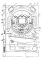
図1に示すように、パチンコ遊技機1は、額縁状に形成されたガラス扉枠2を有する。ガラス扉枠2の下部表面には打球供給皿3がある。打球供給皿3の下部には、打球供給皿3からあふれた景品玉を貯留する余剰玉受皿4と打球を発射する打球操作ハンドル(操作ノブ)5が設けられている。ガラス扉枠2の後方には、遊技盤6が着脱可能に取り付けられている。また、遊技盤6の前面には遊技領域7が設けられている。
【0024】
遊技領域7の中央付近には、複数種類の図柄を可変表示するための可変表示部9と7セグメントLEDによる可変表示器10とを含む可変表示装置8が設けられている。この実施の形態では、可変表示部9には、「左」、「中」、「右」の3つの図柄表示エリアがある。可変表示装置8の側部には、打球を導く通過ゲート11が設けられている。通過ゲート11を通過した打球は、玉出口13を経て始動入賞口14の方に導かれる。通過ゲート11と玉出口13との間の通路には、通過ゲート11を通過した打球を検出するゲートスイッチ12がある。また、始動入賞口14に入った入賞球は、遊技盤6の背面に導かれ、始動口スイッチ17によって検出される。また、始動入賞口14の下部には開閉動作を行う可変入賞球装置15が設けられている。可変入賞球装置15は、ソレノイド16によって開状態とされる。
【0025】
可変入賞球装置15の下部には、特定遊技状態(大当り状態)においてソレノイド21によって開状態とされる開閉板20が設けられている。この実施の形態では、開閉板20が大入賞口を開閉する手段となる。開閉板20から遊技盤6の背面に導かれた入賞球のうち一方(Vゾーン)に入った入賞球はVカウントスイッチ22で検出される。また、開閉板20からの入賞球はカウントスイッチ23で検出される。可変表示装置8の下部には、始動入賞口14に入った入賞球数を表示する4個の表示部を有する始動入賞記憶表示器18が設けられている。この例では、4個を上限として、始動入賞がある毎に、始動入賞記憶表示器18は点灯している表示部を1つずつ増やす。そして、可変表示部9の可変表示が開始される毎に、点灯している表示部を1つ減らす。
【0026】
遊技盤6には、複数の入賞口19,24が設けられ、遊技球の入賞口19,24への入賞は入賞口スイッチ19a,24aによって検出される。遊技領域7の左右周辺には、遊技中に点滅表示される装飾ランプ25が設けられ、下部には、入賞しなかった打球を吸収するアウト口26がある。また、遊技領域7の外側の左右上部には、効果音を発する2つのスピーカ27が設けられている。遊技領域7の外周には、遊技効果LED28aおよび遊技効果ランプ28b,28cが設けられている。
【0027】
そして、この例では、一方のスピーカ27の近傍に、賞球残数があるときに点灯する賞球ランプ51が設けられ、他方のスピーカ27の近傍に、補給玉が切れたときに点灯する球切れランプ52が設けられている。さらに、図1には、パチンコ遊技台1に隣接して設置され、プリペイドカードが挿入されることによって球貸しを可能にするカードユニット50も示されている。
【0028】
カードユニット50には、使用可能状態であるか否かを示す使用可表示ランプ151、カード内に記録された残額情報に端数(100円未満の数)が存在する場合にその端数を打球供給皿3の近傍に設けられる度数表示LEDに表示させるための端数表示スイッチ152、カードユニット50がいずれの側のパチンコ遊技機1に対応しているのかを示す連結台方向表示器153、カードユニット50内にカードが投入されていることを示すカード投入表示ランプ154、記録媒体としてのカードが挿入されるカード挿入口155、およびカード挿入口155の裏面に設けられているカードリーダライタの機構を点検する場合にカードユニット50を解放するためのカードユニット錠156が設けられている。
【0029】
打球発射装置から発射された打球は、打球レールを通って遊技領域7に入り、その後、遊技領域7を下りてくる。打球が通過ゲート11を通ってゲートスイッチ12で検出されると、可変表示器10の表示数字が連続的に変化する状態になる。また、打球が始動入賞口14に入り始動口スイッチ17で検出されると、図柄の変動を開始できる状態であれば、可変表示部9内の図柄が回転を始める。図柄の変動を開始できる状態でなければ、始動入賞記憶を1増やす。
【0030】
可変表示部9内の画像の回転は、一定時間が経過したときに停止する。停止時の画像の組み合わせが大当り図柄の組み合わせであると、大当り遊技状態に移行する。すなわち、開閉板20が、一定時間経過するまで、または、所定個数(例えば10個)の打球が入賞するまで開放する。そして、開閉板20の開放中に打球が特定入賞領域に入賞しVカウントスイッチ22で検出されると、継続権が発生し開閉板20の開放が再度行われる。継続権の発生は、所定回数(例えば15ラウンド)許容される。
【0031】
停止時の可変表示部9内の画像の組み合わせが確率変動を伴う大当り図柄の組み合わせである場合には、次に大当りとなる確率が高くなる。すなわち、高確率状態という遊技者にとってさらに有利な状態となる。また、可変表示器10における停止図柄が所定の図柄(当り図柄)である場合に、可変入賞球装置15が所定時間だけ開状態になる。さらに、高確率状態では、可変表示器10における停止図柄が当り図柄になる確率が高められるとともに、可変入賞球装置15の開放時間と開放回数が高められる。
【0032】
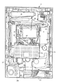
次に、パチンコ遊技機1の裏面の構造について図2を参照して説明する。
可変表示装置8の背面では、図2に示すように、機構板36の上部に景品玉タンク38が設けられ、パチンコ遊技機1が遊技機設置島に設置された状態でその上方から景品玉が景品玉タンク38に供給される。景品玉タンク38内の景品玉は、誘導樋39を通って玉払出装置に至る。
【0033】
機構板36には、中継基板30を介して可変表示部9を制御する可変表示制御ユニット29、基板ケース32に覆われ遊技制御用マイクロコンピュータ等が搭載された遊技制御基板(主基板)31、可変表示制御ユニット29と遊技制御基板31との間の信号を中継するための中継基板33、および景品玉の払出制御を行う賞球制御用マイクロコンピュータ等が搭載された賞球制御基板37が設置されている。さらに、機構板36の下部には、モータの回転力を利用して打球を遊技領域7に発射する打球発射装置34と、遊技効果ランプ・LED28a,28b,28c、賞球ランプ51および球切れランプ52に信号を送るためのランプ制御基板35が設置されている。
【0034】
また、図3はパチンコ遊技機1の機構板を背面からみた背面図である。誘導樋39を通った玉は、図3に示されるように、球切れ検出器187a,187bを通過して玉供給樋186a,186bを経て玉払出装置97に至る。玉払出装置97から払い出された景品玉は、連絡口45を通ってパチンコ遊技機1の前面に設けられている打球供給皿3に供給される。連絡口45の側方には、パチンコ遊技機1の前面に設けられている余剰玉受皿4に連通する余剰玉通路46が形成されている。入賞にもとづく景品玉が多数払い出されて打球供給皿3が満杯になり、ついには景品玉が連絡口45に到達した後さらに景品玉が払い出されると景品玉は、余剰玉通路46を経て余剰玉受皿4に導かれる。さらに景品玉が払い出されると、感知レバー47が満タンスイッチ48を押圧して満タンスイッチ48がオンする。その状態では、玉払出装置97内のステッピングモータの回転が停止して玉払出装置97の動作が停止するとともに、必要に応じて打球発射装置34の駆動も停止する。
【0035】
賞球払出制御を行うために、入賞口スイッチ19a,24a、始動口スイッチ17およびVカウントスイッチ22からの信号が、主基板31に送られる。主基板31のCPU56は、始動口スイッチ17がオンすると6個の賞球払出に対応した入賞が発生したことを知る。また、カウントスイッチ23がオンすると15個の賞球払出に対応した入賞が発生したことを知る。そして、入賞口スイッチがオンすると10個の賞球払出に対応した入賞が発生したことを知る。なお、この実施の形態では、例えば、入賞口24に入賞した遊技球は、入賞口24からの入賞球流路に設けられている入賞口スイッチ24aで検出され、入賞口19に入賞した遊技球は、入賞口19からの入賞球流路に設けられている入賞口スイッチ19aで検出される。
【0036】
図4は、主基板31における回路構成の一例を示すブロック図である。なお、図4には、賞球制御基板37、ランプ制御基板35、音制御基板70、発射制御基板91および表示制御基板80も示されている。主基板31には、プログラムに従ってパチンコ遊技機1を制御する基本回路53と、ゲートスイッチ12、始動口スイッチ17、Vカウントスイッチ22、カウントスイッチ23および入賞口スイッチ19a,24aからの信号を基本回路53に与えるスイッチ回路58と、可変入賞球装置15を開閉するソレノイド16および開閉板20を開閉するソレノイド21を基本回路53からの指令に従って駆動するソレノイド回路59と、始動記憶表示器18の点灯および滅灯を行うとともに7セグメントLEDによる可変表示器10と装飾ランプ25とを駆動するランプ・LED回路60とが搭載されている。
【0037】
また、基本回路53から与えられるデータに従って、大当りの発生を示す大当り情報、可変表示部9の画像表示開始に利用された始動入賞球の個数を示す有効始動情報、確率変動が生じたことを示す確変情報等をホール管理コンピュータ等のホストコンピュータに対して出力する情報出力回路64を含む。
【0038】
基本回路53は、ゲーム制御用のプログラム等を記憶するROM54、ワークメモリとして使用される記憶手段の一例であるRAM55、制御用のプログラムに従って制御動作を行うCPU56およびI/Oポート部57を含む。この実施の形態では、ROM54,RAM55はCPU56に内蔵されている。すなわち、CPU56は、1チップマイクロコンピュータである。なお、1チップマイクロコンピュータは、少なくともRAM55が内蔵されていればよく、ROM54およびI/Oポート部57は外付けであっても内蔵されていてもよい。また、I/Oポート部57は、マイクロコンピュータにおける情報入出力可能な端子である。
【0039】
さらに、主基板31には、電源投入時に基本回路53をリセットするための初期リセット回路65と、基本回路53から与えられるアドレス信号をデコードしてI/Oポート部57のうちのいずれかのI/Oポートを選択するための信号を出力するアドレスデコード回路67とが設けられている。
なお、玉払出装置97から主基板31に入力されるスイッチ情報もあるが、図4ではそれらは省略されている。
【0040】
遊技球を打撃して発射する打球発射装置は発射制御基板91上の回路によって制御される駆動モータ94で駆動される。そして、駆動モータ94の駆動力は、操作ノブ5の操作量に従って調整される。すなわち、発射制御基板91上の回路によって、操作ノブ5の操作量に応じた速度で打球が発射されるように制御される。
【0041】
図5は、表示制御基板80内の回路構成を、可変表示部9の一実現例であるCRT82および主基板31の出力ポート(ポートA,B)571,572および出力バッファ回路63とともに示すブロック図である。出力ポート571からは8ビットのデータが出力され、出力ポート572からは1ビットのストローブ信号(INT信号)が出力される。
【0042】
表示制御用CPU101は、制御データROM102に格納されたプログラムに従って動作し、主基板31からノイズフィルタ107および入力バッファ回路105を介してストローブ信号が入力されると、入力バッファ回路105を介して表示制御コマンドを受信する。入力バッファ回路105として、例えば汎用ICである74HC244を使用することができる。なお、表示制御用CPU101がI/Oポートを内蔵していない場合には、入力バッファ回路105と表示制御用CPU101との間に、I/Oポートが設けられる。
【0043】
そして、表示制御用CPU101は、受信した表示制御コマンドに従って、CRT82に表示される画面の表示制御を行う。具体的には、表示制御コマンドに応じた指令をVDP103に与える。VDP103は、キャラクタROM86から必要なデータを読み出す。VDP103は、入力したデータに従ってCRT82に表示するための画像データを生成し、その画像データをVRAM87に格納する。そして、VRAM87内の画像データは、R,G,B信号に変換され、D−A変換回路104でアナログ信号に変換されてCRT82に出力される。この例では、可変表示装置としてCRTを例示するが、可変表示部は、他の装置、例えば液晶表示装置で実現されていてもよい。
【0044】
なお、図5には、VDP103をリセットするためのリセット回路83、VDP103に動作クロックを与えるための発振回路85、および使用頻度の高い画像データを格納するキャラクタROM86も示されている。キャラクタROM86に格納される使用頻度の高い画像データとは、例えば、CRT82に表示される人物、動物、または、文字、図形もしくは記号等からなる画像などである。この実施の形態では、表示制御用CPU101は、1チップマイクロコンピュータであり、少なくともRAMが内蔵されている。
【0045】
図6は、賞球制御基板37および玉払出装置97の構成要素などの賞球に関連する構成要素を示すブロック図である。図6に示すように、満タンスイッチ48からの検出信号は、中継基板71を介して主基板31のI/Oポート57に入力される。満タンスイッチ48は、余剰玉受皿4の満タンを検出するスイッチである。
【0046】
球切れスイッチ187(187a,187b)からの検出信号は、中継基板72および中継基板71を介して主基板31のI/Oポート57に入力される。球切れスイッチ187は、景品玉通路内の景品玉の有無を検出するスイッチである。
【0047】
主基板31のCPU56は、球切れスイッチ187からの検出信号が球切れ状態を示しているか、または、満タンスイッチ48からの検出信号が満タン状態を示していると、球貸し禁止を指示する賞球制御コマンドを送出する。球貸し禁止を指示する賞球制御コマンドを受信すると、賞球制御基板37の賞球制御用CPU371は、球貸し処理を停止する。
【0048】
さらに、賞球カウントスイッチ301Aからの検出信号も、中継基板72および中継基板71を介して主基板31のI/Oポート57に入力される。また、主基板31のI/Oポート57から入賞球排出ソレノイド127への駆動信号は、中継基板71を介して入賞球排出ソレノイド127に供給される。なお、賞球カウントスイッチ301Aは、玉払出装置97の賞球機構部分に設けられ、実際に払い出された賞球を検出する。
【0049】
入賞があると、賞球制御基板37には、主基板31の出力ポート(ポートG,H)577,578から賞球個数を示す賞球制御コマンドが入力される。出力ポート577は8ビットのデータを出力し、出力ポート578は1ビットのストローブ信号(INT信号)を出力する。賞球個数を示す賞球制御コマンドは、入力バッファ回路373を介してI/Oポート372aに入力される。賞球制御用CPU371は、I/Oポート372aを介して賞球制御コマンドを入力し、賞球制御コマンドに応じて玉払出装置97を駆動して賞球払出を行う。なお、この実施の形態では、賞球制御用CPU371は、1チップマイクロコンピュータであり、少なくともRAMが内蔵されている。
【0050】
また、賞球制御用CPU371は、出力ポート372gを介して、貸し玉数を示す球貸し個数信号をターミナル基板160に出力し、ブザー駆動信号をブザー基板75に出力する。ブザー基板75にはブザーが搭載されている。さらに、出力ポート372eを介して、エラー表示用LED374にエラー信号を出力する。
【0051】
さらに、賞球制御基板37の入力ポート372bには、中継基板72を介して、賞球カウントスイッチ301Aの検出信号および球貸しカウントスイッチ301Bの検出信号が入力される。球貸しカウントスイッチ301Bは、実際に貸し出された遊技球を検出する。賞球制御基板37からの払出モータ289への駆動信号は、出力ポート372cおよび中継基板72を介して玉払出装置97の賞球機構部分における払出モータ289に伝えられる。
【0052】
カードユニット50には、カードユニット制御用マイクロコンピュータが搭載されている。また、カードユニット50には、端数表示スイッチ152、連結台方向表示器153、カード投入表示ランプ154およびカード挿入口155が設けられている(図1参照)。残高表示基板74には、打球供給皿3の近傍に設けられている度数表示LED、球貸しスイッチおよび返却スイッチが接続される。
【0053】
残高表示基板74からカードユニット50には、遊技者の操作に応じて、球貸しスイッチ信号および返却スイッチ信号が賞球制御基板37を介して与えられる。また、カードユニット50から残高表示基板74には、プリペイドカードの残高を示すカード残高表示信号および球貸し可表示信号が賞球制御基板37を介して与えられる。カードユニット50と賞球制御基板37の間では、ユニット操作信号(BRDY信号)、球貸し要求信号(BRQ信号)、球貸し完了信号(EXS信号)およびパチンコ機動作信号(PRDY信号)がI/Oポート372fを介してやりとりされる。
【0054】
パチンコ遊技機1の電源が投入されると、賞球制御基板37の賞球制御用CPU371は、カードユニット50にPRDY信号を出力する。カードユニット50においてカードが受け付けられ、球貸しスイッチが操作され球貸しスイッチ信号が入力されると、カードユニット制御用マイクロコンピュータは、賞球制御基板37にBRDY信号を出力する。この時点から所定の遅延時間が経過すると、カードユニット制御用マイクロコンピュータは、賞球制御基板37にBRQ信号を出力する。そして、賞球制御基板37の賞球制御用CPU371は、払出モータ289を駆動し、所定個の貸し玉を遊技者に払い出す。そして、払出が完了したら、賞球制御用CPU371は、カードユニット50にEXS信号を出力する。
【0055】
以上のように、カードユニット50からの信号は全て賞球制御基板37に入力される構成になっている。従って、球貸し制御に関して、カードユニット50から主基板31に信号が入力されることはなく、主基板31の基本回路53にカードユニット50の側から不正に信号が入力される余地はない。なお、主基板31および賞球制御基板37には、ソレノイドおよびモータやランプを駆動するためのドライバ回路が搭載されているが、図6では、それらの回路は省略されている。
【0056】
この実施の形態では、少なくとも主基板31および賞球制御基板37において、CPUが内蔵するRAMの一部が電源バックアップされている。すなわち、遊技機に対する電力供給が停止しても、バックアップRAM領域のデータは保存される。また、表示制御用CPU101、音声制御用CPU701、ランプ制御用CPU351においても、RAMの一部が電源バックアップされるように構成されていてもよい。
【0057】
図7は、電源監視および電源バックアップのためのCPU56周りの一構成例を示すブロック図である。図7に示すように、第1の電源監視回路(第1の電源監視手段)からの電圧低下信号が、バッファ回路900を介してCPU56のマスク不能割込端子(NMI端子)に接続されている。第1の電源監視回路は、遊技機が使用する各種直流電源のうちのいずれかの電源の電圧を監視して電源電圧低下を検出する回路である。この実施の形態では、VSLの電源電圧を監視して電圧値が所定値以下になるとローレベルの電圧低下信号を発生する。VSLは、遊技機で使用される直流電圧のうちで最も高い電圧であり、この例では+30Vである。従って、CPU56は、割込処理によって電源断の発生を確認することができる。なお、この実施の形態では、第1の電源監視回路は、後述する電源基板に搭載されている。
【0058】
電気部品制御基板には、初期リセット回路65も示されているが、この実施の形態では、初期リセット回路65は、第2の電源監視回路(第2の電源監視手段)も兼ねている。すなわち、リセットIC651は、電源投入時に、外付けのコンデンサに容量で決まる所定時間だけ出力をローレベルとし、所定時間が経過すると出力をハイレベルにする。また、リセットIC651は、第1の電源監視回路が監視する電源電圧と等しい電源電圧であるVSLの電源電圧を電圧低下監視用端子に導入し、その端子の電圧を監視して電圧値が所定値以下になるとローレベルの電圧低下信号を発生する。なお、図7に示すように、この電圧低下信号はリセット信号と同じ出力信号である。
【0059】
図7に示すように、リセットIC651からのリセット信号は、NAND回路947に入力されるとともに、反転回路(NOT回路)944を介してカウンタIC941のクリア端子に入力される。カウンタIC941は、クリア端子への入力がローレベルになると、発振器943からのクロック信号をカウントする。そして、カウンタIC941のQ5出力がNOT回路945,946を介してNAND回路947に入力される。また、カウンタIC941のQ6出力は、フリップフロップ(FF)942のクロック端子に入力される。フリップフロップ942のD入力はハイレベルに固定され、Q出力は論理和回路(OR回路)949に入力される。OR回路949の他方の入力には、NAND回路947の出力がNOT回路948を介して導入される。そして、OR回路949の出力がCPU56のリセット端子に接続されている。
【0060】
そして、例えば、第1の電源監視回路の検出電圧(電圧低下信号を出力することになる電圧)を+22Vとし、第2の電源監視回路の検出電圧を+9Vとする。そのように構成した場合には、第1の電源監視回路と第2の電源監視回路とは、同一の電源VSLの電圧を監視するので、第1の電圧監視回路が電圧低下信号を出力するタイミングと第2の電圧監視回路が電圧低下信号を出力するタイミングの差を所望の所定期間に確実に設定することができる。所望の所定期間とは、第1の電源監視回路からの電圧低下信号に応じて電力供給停止時処理を開始してから電力供給停止時処理が確実に完了するまでの期間である。
【0061】
この例では、第1の電源監視手段が検出信号を出力することになる第1検出条件は+30V電源電圧が+22Vにまで低下したことであり、第2の電源監視手段が検出信号を出力することになる第2検出条件は+30V電源電圧が+9Vにまで低下したことになる。ただし、ここで用いられている電圧値は一例であって、他の値を用いてもよい。
【0062】
ただし、監視範囲が狭まるが、第1の電圧監視回路および第2の電圧監視回路の監視電圧として+5V電源電圧を用いることも可能である。その場合にも、第1の電圧監視回路の検出電位は、第2の電圧監視回路の検出電位よりも高く設定される。
【0063】
CPU56等の駆動電源である+5V電源から電力が供給されていない間、RAMの少なくとも一部は、電源基板から供給されるバックアップ電源によってバックアップされ、遊技機に対する電源が断しても内容は保存される。そして、+5V電源が復旧すると、初期リセット回路65からリセット信号が発せられるので、CPU56は、通常の動作状態に復帰する。そのとき、必要なデータがバックアップされているので、停電等からの復旧時には停電発生時の遊技状態に復帰することができる。
【0064】
図8は、遊技機の電源基板910の一構成例を示すブロック図である。電源基板910は、主基板31、表示制御基板80、音声制御基板70、ランプ制御基板35および賞球制御基板37等の電気部品制御基板と独立して設置され、遊技機内の各電気部品制御基板および機構部品が使用する電圧を生成する。この例では、AC24V、VSL(DC+30V)、DC+21V、DC+12VおよびDC+5Vを生成する。また、バックアップ電源となるコンデンサ916は、DC+5Vすなわち各基板上のIC等を駆動する電源のラインから充電される。
【0065】
トランス911は、交流電源からの交流電圧を24Vに変換する。AC24V電圧は、コネクタ915に出力される。また、整流回路912は、AC24Vから+30Vの直流電圧を生成し、DC−DCコンバータ913およびコネクタ915に出力する。DC−DCコンバータ913は、+21V、+12Vおよび+5Vを生成してコネクタ915に出力する。コネクタ915は例えば中継基板に接続され、中継基板から各電気部品制御基板および機構部品に必要な電圧の電力が供給される。なお、トランス911の入力側には、遊技機に対する電源供給を停止したり開始させたりするための電源スイッチ918が設置されている。
【0066】
DC−DCコンバータ913からの+5Vラインは分岐してバックアップ+5Vラインを形成する。バックアップ+5Vラインとグラウンドレベルとの間には大容量のコンデンサ916が接続されている。コンデンサ916は、遊技機に対する電力供給が遮断されたときの電気部品制御基板のバックアップRAM(電源バックアップされているRAMすなわち記憶内容保持状態となりうる記憶手段)に対して記憶状態を保持できるように電力を供給するバックアップ電源となる。また、+5Vラインとバックアップ+5Vラインとの間に、逆流防止用のダイオード917が挿入される。
【0067】
なお、バックアップ電源として、+5V電源から充電可能な電池を用いてもよい。電池を用いる場合には、+5V電源から電力供給されない状態が所定時間継続すると容量がなくなるような充電池が用いられる。
【0068】
また、電源基板910には、上述した第1の電源回路を構成する電源監視用IC902が搭載されている。電源監視用IC902は、VSL電源電圧を導入し、VSL電源電圧を監視することによって電源断の発生を検出する。具体的には、VSL電源電圧が所定値(この例では+22V)以下になったら、電源断が発生することを知らせるために電圧低下信号を出力する。なお、監視対象の電源電圧は、各電気部品制御基板に搭載されている回路素子の電源電圧(この例では+5V)よりも高い電圧であることが好ましい。この例では、交流から直流に変換された直後の電圧であるVSLが用いられている。電源監視用IC902からの電圧低下信号は、主基板31や賞球制御基板37等に供給される。
【0069】
電源監視用IC902が電源断を検知するための所定値は、通常時の電圧より低いが、各電気部品制御基板上のCPUが暫くの間動作しうる程度の電圧である。また、電源監視用IC902が、CPU等の回路素子を駆動するための電圧(この例では+5V)よりも高く、また、交流から直流に変換された直後の電圧を監視するように構成されているので、CPUが必要とする電圧に対して監視範囲を広げることができる。従って、より精密な監視を行うことができる。さらに、監視電圧としてVSL(+30V)を用いる場合には、遊技機の各種スイッチに供給される電圧が+12Vであることから、電源瞬断時のスイッチオン誤検出の防止も期待できる。すなわち、+30V電源の電圧を監視すると、+30V作成の以降に作られる+12Vが落ち始める以前の段階でそれの低下を検出できる。よって、+12V電源の電圧が低下するとスイッチ出力がオン状態を呈するようになるが、+12Vより早く低下する+30V電源電圧を監視して電源断を認識すれば、スイッチ出力がオン状態を呈する前に電源復旧待ちの状態に入ってスイッチ出力を検出しない状態となることができる。
【0070】
また、電源監視用IC902は、電気部品制御基板とは別個の電源基板910に搭載されているので、第1の電源監視回路から複数の電気部品制御基板に電圧低下信号を供給することができる。電圧低下信号を必要とする電気部品制御基板が幾つあっても第1の電源監視手段は1つ設けられていればよいので、各電気部品制御基板における各電気部品制御手段が後述する復帰制御を行っても、遊技機のコストはさほど上昇しない。
【0071】
なお、図8に示された構成では、電源監視用IC902の検出出力(電圧低下信号)は、バッファ回路918,919を介してそれぞれの電気部品制御基板(例えば主基板31と賞球制御基板37)に伝達されるが、例えば、1つの検出出力を中継基板に伝達し、中継基板から各電気部品制御基板に同じ信号を分配する構成でもよい。また、電圧低下信号を必要とする基板数に応じたバッファ回路を設けてもよい。
【0072】
図9は、図7に示された初期リセット回路65のリセットIC651とその周辺のICの出力信号の様子を示すタイミング図である。図9に示すように、リセットIC651の出力は、+5V電源電圧のレベルが所定値を越えるとハイレベルになる。リセットIC651の出力がハイレベルになると、カウンタIC941のクリア状態が解除されるので、カウンタIC941は発振器943の出力クロック信号のカウントを開始する。発振器943の発振周波数は例えば11.776MHzである。なお、発振器943の出力クロック信号は、CPU901の外部クロック端子にも供給されている。
【0073】
カウンタIC941が16クロックをカウントするとQ5出力が立ち上がる。また、32クロックをカウントするとQ6出力がハイレベルに立ち上がる。カウンタIC941のQ6出力が立ち上がると、FF942の出力がハイレベルになる。IC947は、カウンタIC941のQ6出力とリセットIC651の出力との論理積を反転して、図9に示すような信号を出力する。OR回路949は、IC947の出力を反転するIC948の出力とFF942の出力との論理和をとって、図9に示すような信号を出力する。
【0074】
従って、遊技機の電源オン時には、CPU901のリセット端子に対して、一旦リセット解除状態(ハイレベル)になってから、再度リセット状態(ローレベル)になるような信号が供給される。すなわち、電源オン時には、CPU901をリセット状態とするようなローレベル信号が2回発生することになる。また、リセット解除を示すハイレベルが2回発生しているということもできる。その結果、CPU901は、最初のリセット解除を示すローレベルからハイレベルへの変化によって起動しなかったとしても、2回目のローレベルからハイレベルへの変化によって確実に起動することができる。よって、遊技機の電源投入時に、確実に遊技制御が開始される。
【0075】
なお、IC949が出力するハイレベルパルス(リセット解除状態に相当)およびローレベルパルス(リセット状態に相当)の幅は、カウンタIC941の出力端子を変更するによって任意に設定することができる。ただし、IC949が出力するハイレベルパルスの幅は、CPU901にも供給されている発振器943の出力クロックの数クロック分(例えば4クロック)以上であることが好ましいが、この例では、16クロック分となっている。また、IC949が出力するローレベルパルスの幅は、発振器943の出力クロックの数クロック分(例えば4クロック)以上であることが好ましいが、この例では、16クロック分となっている。
【0076】
CPU901は、リセット状態が解除されて動作を開始すると、本来の制御処理を開始する前に、セキュリティチェックなどの所定の起動時処理を行うように構成されている場合がある。すると、IC949が出力するハイレベルパルスの終了時点(立ち下がり時点)は、所定の起動時処理の完了前(本来の制御処理開始前)であることが望ましい。さもないと、IC949の出力が立ち上がって所定の起動時処理が行われ、さらに本来の制御処理が開始されてからIC949の出力がローレベルになることになり、本来の処理開始後に、再度CPU901がリセットされる状況になるからである。IC949が出力するハイレベルパルスの終了時点(立ち下がり時点)は、例えば立ち上がり時点から100ms以内であることが好ましいが、図7に示された回路構成では、100ms以内になっている。
【0077】
また、電源断時には、リセットIC651に入力されているVSL(この例では+30V電源電圧)の電位が所定値(この例では+9V)を下回ると、リセットIC651の出力がローレベルになる。すると、FF942のクリア端子(CLR)にローレベルが入力されFF942のQ出力はローレベルになる。よって、OR回路949の出力はローレベルになり、CPU901のリセット端子にリセット状態を示すレベルが供給される。すなわち、図7に示された回路構成では、リセットIC651の出力がローレベルになると、直ちにCPU901のリセット端子の入力状態がローレベルに固定される。換言すれば、電源断時には、2回のリセットパルスがCPU901に与えられるようなことはない。
【0078】
なお、この実施の形態では、図9の最下段に示されたような信号状態を作成するために図7に示されたような回路構成を用いたが、そのような信号状態を作成するために他の回路構成を用いてもよい。
【0079】
また、リセット状態を示すレベルを2回与えなくても確実に起動することが補償されているCPU56を用いる場合には、図7における符号941〜949で示されている回路要素は不要であり、リセットIC651の出力をそのままCPU56のリセット端子に供給すればよい。また、この実施の形態では、第2の電源監視手段は初期リセット手段と兼用されているが、それらを別々の回路要素で実現してもよい。
【0080】
図10は、遊技機の電源断時の電源低下やNMI信号(=電源断信号:第1の電圧低下信号)の様子を示すタイミング図である。遊技機に対する電力供給が断たれると、最も高い直流電源電圧であるVSLの電圧値は徐々に低下する。そして、この例では、+22Vにまで低下すると、電源基板910に搭載されてる電源監視用IC902から電源断信号(電圧低下信号)が出力される(ローレベルになる)。
【0081】
電源断信号は、電気部品制御基板(この実施の形態では主基板31および賞球制御基板37)に導入され、CPU56および賞球制御用CPU371のNMI端子に入力される。CPU56および賞球制御用CPU371は、後述するNMI処理によって、所定の電力供給停止時処理を実行する。
【0082】
VSLの電圧値がさらに低下して所定値(この例では+9V)にまで低下すると、主基板31や賞球制御基板37に搭載されているリセットIC651の出力がローレベルになり、CPU56および賞球制御用CPU371がシステムリセット状態になる。なお、CPU56および賞球制御用CPU371は、システムリセット状態とされる前に、電力供給停止時処理を完了している。
【0083】
VSLの電圧値がさらに低下してVcc(各種回路を駆動するための+5V)を生成することが可能な電圧を下回ると、各基板において各回路が動作できない状態となる。しかし、少なくとも主基板31や賞球制御基板37では、電力供給停止時処理が実行され、CPU56および賞球制御用CPU371がシステムリセット状態とされている。
【0084】
以上のように、この実施の形態では、第1の電源監視回路は、遊技機で使用される直流電圧のうちで最も高い電源VSLの電圧を監視して、その電源の電圧が所定値を下回ったら電圧低下信号(電源断検出信号)を発生する。図10に示すように、電源断検出信号が出力されるタイミングでは、IC駆動電圧は、まだ各種回路素子を十分駆動できる電圧値になっている。従って、IC駆動電圧で動作する主基板31のCPU56が所定の電力供給停止時処理を行うための動作時間が確保されている。
【0085】
なお、ここでは、第1の電源監視回路は、遊技機で使用される直流電圧のうちで最も高い電源VSLの電圧を監視したが、電源断検出信号を発生するタイミングが、IC駆動電圧で動作する電気部品制御手段が所定の電力供給停止時処理を行うための動作時間が確保されるようなタイミングであれば、監視対象電圧は、最も高い電源VSLの電圧でなくてもよい。すなわち、少なくともIC駆動電圧よりも高い電圧を監視すれば、電気部品制御手段が所定の電力供給停止時処理を行うための動作時間が確保されるようなタイミングで電源断検出信号を発生することができる。
【0086】
その場合、上述したように、監視対象電圧は、遊技機の各種スイッチに供給される電圧が+12Vであることから、電源断時のスイッチオン誤検出の防止も期待できる電圧であることが好ましい。すなわち、スイッチに供給される電圧(スイッチ電圧)である+12V電源電圧が落ち始める以前の段階で、電圧低下を検出できることが好ましい。よって、少なくともスイッチ電圧よりも高い電圧を監視することが好ましい。
【0087】
以下、遊技機の制御動作について説明する。
図11は、主基板31におけるCPU56が実行するメイン処理を示すフローチャートである。遊技機に対する電源が投入されると、メイン処理において、CPU56は、まず、停電からの復旧時であったか否か確認する(ステップS1)。停電からの復旧時であったか否かは、例えば、電源断時にバックアップRAM領域に設定される電源断フラグによって確認される。
【0088】
停電からの復旧時であった場合には、バックアップRAM領域のデータチェック(この例ではパリティチェック)を行う(ステップS3)。不測の電源断が生じた後に復旧した場合には、バックアップRAM領域のデータは保存されていたはずであるから、チェック結果は正常になる。チェック結果が正常でない場合には、内部状態を電源断時の状態に戻すことができないので、停電復旧時でない電源投入時に実行される初期化処理を実行する(ステップS4,S2)。
【0089】
チェック結果が正常であれば、CPU56は、内部状態を電源断時の状態に戻すための遊技状態復旧処理を行うとともに(ステップS5)、電源断フラグをクリアする(ステップS6)。
【0090】
停電からの復旧時でない場合には、CPU56は、通常の初期化処理を実行する(ステップS1,S2)。その後、メイン処理では、タイマ割込フラグの監視(ステップS6)の確認が行われるループ処理に移行する。なお、ループ内では、表示用乱数更新処理(ステップS7)も実行される。
【0091】
なお、ここでは、ステップS1で停電からの復旧か否かを確認し、停電からの復旧時であればパリティチェックを行ったが、最初に、パリティチェックを実行し、チェック結果が正常でなければ停電からの復旧ではないと判断してステップS2の初期化処理を実行し、チェック結果が正常であれば遊技状態復帰処理を行ってもよい。すなわち、パリティチェックの結果をもって停電からの復旧であるか否かを判断してもよい。
【0092】
また、停電復旧処理を実行するか否か判断する場合に、すなわち、遊技状態を復旧するか否か判断する際に、保存されていたRAMデータにおける特別プロセスフラグ等や始動入賞記憶数データによって、遊技機が遊技待機状態(図柄変動中でなく、大当り遊技中でなく、確変中でなく、また、始動入賞記憶がない状態)であることが確認されたら、遊技状態復旧処理を行わずに初期化処理を実行するようにしてもよい。
【0093】
通常の初期化処理では、図12に示すように、レジスタおよびRAMのクリア処理(ステップS2a)と、必要な初期値設定処理(ステップS2b)が行われた後に、2ms毎に定期的にタイマ割込がかかるようにCPU56に設けられているタイマレジスタの初期設定(タイムアウトが2msであることと繰り返しタイマが動作する設定)が行われる(ステップS2c)。すなわち、ステップS2cで、タイマ割込を能動化する処理と、タイマ割込インタバルを設定する処理とが実行される。
【0094】
従って、この実施の形態では、CPU56の内部タイマが繰り返しタイマ割込を発生するように設定される。この実施の形態では、繰り返し周期は2msに設定される。そして、図13に示すように、タイマ割込が発生すると、CPU56は、タイマ割込フラグをセットする(ステップS11)。
【0095】
CPU56は、ステップS8において、タイマ割込フラグがセットされたことを検出すると、タイマ割込フラグをリセットするとともに(ステップS9)、遊技制御処理を実行する(ステップS10)。以上の制御によって、この実施の形態では、遊技制御処理は2ms毎に起動されることになる。なお、この実施の形態では、タイマ割込処理ではフラグセットのみがなされ、遊技制御処理はメイン処理において実行されるが、タイマ割込処理で遊技制御処理を実行してもよい。
【0096】
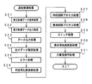
図14は、ステップS10の遊技制御処理を示すフローチャートである。遊技制御処理において、CPU56は、まず、表示制御基板80に送出される表示制御コマンドをRAM55の所定の領域に設定する処理を行った後に(表示制御データ設定処理:ステップS21)、表示制御コマンドを出力する処理を行う(表示制御データ出力処理:ステップS22)。
【0097】
次いで、各種出力データの格納領域の内容を各出力ポートに出力する処理を行う(データ出力処理:ステップS23)。また、ホール管理用コンピュータに出力される大当り情報、始動情報、確率変動情報などの出力データを格納領域に設定する出力データ設定処理を行う(ステップS24)。さらに、パチンコ遊技機1の内部に備えられている自己診断機能によって種々の異常診断処理が行われ、その結果に応じて必要ならば警報が発せられる(エラー処理:ステップS25)。
【0098】
次に、遊技制御に用いられる大当り判定用の乱数等の各判定用乱数を示す各カウンタを更新する処理を行う(ステップS26)。
【0099】
さらに、CPU56は、特別図柄プロセス処理を行う(ステップS27)。特別図柄プロセス制御では、遊技状態に応じてパチンコ遊技機1を所定の順序で制御するための特別図柄プロセスフラグに従って該当する処理が選び出されて実行される。そして、特別図柄プロセスフラグの値は、遊技状態に応じて各処理中に更新される。また、普通図柄プロセス処理を行う(ステップS28)。普通図柄プロセス処理では、7セグメントLEDによる可変表示器10を所定の順序で制御するための普通図柄プロセスフラグに従って該当する処理が選び出されて実行される。そして、普通図柄プロセスフラグの値は、遊技状態に応じて各処理中に更新される。
【0100】
さらに、CPU56は、スイッチ回路58を介して、ゲートセンサ12、始動口センサ17、カウントセンサ23および入賞口スイッチ19a,24aの状態を入力し、各入賞口や入賞装置に対する入賞があったか否か判定する(スイッチ処理:ステップS29)。CPU56は、さらに、停止図柄の種類を決定する乱数等の表示用乱数を更新する処理を行う(ステップS30)。
【0101】
また、CPU56は、賞球制御基板37との間の信号処理を行う(ステップS31)。すなわち、所定の条件が成立すると賞球制御基板37に賞球制御コマンドを出力する。賞球制御基板37に搭載されている賞球制御用CPUは、賞球制御コマンドに応じて玉払出装置97を駆動する。
【0102】
以上のように、メイン処理には遊技制御処理に移行すべきか否かを判定する処理が含まれ、CPU56の内部タイマが定期的に発生するタイマ割込にもとづくタイマ割込処理で遊技制御処理に移行すべきか否かを判定するためのフラグがセットされるので、遊技制御処理の全てが確実に実行される。つまり、遊技制御処理の全てが実行されるまでは、次回の遊技制御処理に移行すべきか否かの判定が行われないので、遊技制御処理中の全ての各処理が実行完了することは保証されている。
【0103】
従来の一般的な遊技制御処理は、定期的に発生する外部割込によって、強制的に最初の状態に戻されていた。図14に示された例に則して説明すると、例えば、ステップS31の処理中であっても、強制的にステップS21の処理に戻されていた。つまり、遊技制御処理中の全ての各処理が実行完了する前に、次回の遊技制御処理が開始されてしまう可能性があった。
【0104】
なお、ここでは、主基板31のCPU56が実行する遊技制御処理は、CPU56の内部タイマが定期的に発生するタイマ割込にもとづくタイマ割込処理でセットされるフラグに応じて実行されたが、定期的に(例えば2ms毎)信号を発生するハードウェア回路を設け、その回路からの信号をCPU56の外部割込端子に導入し、割込信号によって遊技制御処理に移行すべきか否かを判定するためのフラグをセットするようにしてもよい。
【0105】
そのように構成した場合にも、遊技制御処理の全てが実行されるまでは、フラグの判定が行われないので、遊技制御処理中の全ての各処理が実行完了することが保証される。
【0106】
図15は、電源基板910の第1の電源監視回路からの電圧低下信号にもとづくNMIに応じて実行される停電発生NMI処理の一例を示すフローチャートである。停電発生NMI処理において、CPU56は、まず、割込禁止に設定する(ステップS41)。停電発生NMI処理ではRAM内容の保存を確実にするためにチェックサムの生成処理を行う。その処理中に他の割込処理が行われたのではチェックサムの生成処理が完了しないうちにCPUが動作し得ない電圧にまで低下してしまうことがことも考えられるので、まず、他の割込が生じないような設定がなされる。停電発生NMI処理におけるステップS44〜S50は、電力供給停止時処理の一例である。
【0107】
なお、割込処理中では他の割込がかからないような仕様のCPUを用いている場合には、ステップS41の処理は不要である。
【0108】
次いで、CPU56は、電源断フラグが既にセットされているか否か確認する(ステップS42)。電源断フラグが既にセットされていれば、以後の処理を行わない。電源断フラグがセットされていなければ、以下の電力供給停止時処理を実行する。すなわち、ステップS44からステップS50の処理を実行する。
【0109】
まず、CPU56は、必要ならば各レジスタの内容をバックアップRAM領域に格納する(ステップS44)。さらに、バックアップRAM領域のバックアップチェックデータ領域に適当な初期値を設定し(ステップS45)、初期値およびバックアップRAM領域のデータについて順次排他的論理和をとって(ステップS46)、最終的な演算値をバックアップパリティデータ領域に設定する(ステップS47)。その後、電源断フラグをセットする(ステップS48)。また、RAMアクセス禁止状態にする(ステップS49)。そして、全ての出力ポートをオフ状態にする(ステップS50)。電源電圧が低下していくときには、各種信号線のレベルが不安定になってRAM内容が化ける可能性があるが、このようにRAMアクセス禁止状態にしておけば、バックアップRAM内のデータが化けることはない。
【0110】
次いで、CPU56は、ループ処理にはいる。すなわち、何らの処理もしない状態になる。従って、図7に示されたリセットIC651からのリセット信号によって外部から動作禁止状態にされる前に、内部的に動作停止状態になる。よって、電源断時に確実にCPU56は動作停止する。その結果、上述したRAMアクセス禁止の制御および動作停止制御によって、電源電圧が低下していくことに伴って生ずる可能性がある異常動作に起因するRAMの内容破壊等を確実に防止することができる。
【0111】
なお、この実施の形態では、停電発生NMI処理では最終部でプログラムをループ状態にしたが、ホールト(HALT)命令を発行するように構成してもよい。
【0112】
また、RAMアクセス禁止にする前にセットされる電源断フラグは、上述したように、電源投入時において停電からの復旧か否かを判断する際に使用される。また、ステップS41からS50の処理は、第2の電源監視手段が電圧低下信号を発生する前に完了する。換言すれば、第2の電源監視手段が電圧低下信号を発生する前に完了するように、第1の電圧監視手段および第2の電圧監視手段の検出電圧の設定が行われている。
【0113】
この実施の形態では、電力供給停止時処理開始時に、電源断フラグの確認が行われる。そして、電源断フラグが既にセットされている場合には電力供給停止時処理を実行しない。上述したように、電源断フラグは、電力供給停止時処理が完了したことを示すフラグである。従って、例えば、リセット待ちのループ状態で何らかの原因で再度NMIが発生したとしても、電力供給停止時処理が重複して実行されてしまうようなことはない。
【0114】
ただし、割込処理中では他の割込がかからないような仕様のCPUを用いている場合には、ステップS42の判断は不要である。
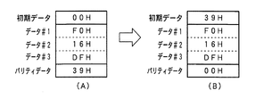
【0115】
図16は、バックアップパリティデータ作成方法を説明するための説明図である。ただし、図16に示す例では、簡単のために、バックアップデータRAM領域のデータのサイズを3バイトとする。電源電圧低下にもとづく停電発生処理において、図16(A)に示すように、バックアップチェックデータ領域に、初期データ(この例では00H)が設定される。次に、「00H」と「F0H」の排他的論理和がとられ、その結果と「16H」の排他的論理和がとられる。さらに、その結果と「DFH」の排他的論理和がとられる。そして、その結果(この例では「39H」)がバックアップパリティデータ領域に設定される。
【0116】
電源が再投入されたときには、停電復旧処理においてパリティ診断が行われるが、図16(B)はパリティ診断の例を示す説明図である。バックアップ領域の全データがそのまま保存されていれば、電源再投入時に、図16(A)に示すようなデータがバックアップ領域に設定されている。
【0117】
ステップS51の処理において、CPU56は、バックアップRAM領域のバックアップパリティデータ領域に設定されていたデータ(この例では「39H」)を初期データとして、バックアップデータ領域の各データについて順次排他的論理和をとる処理を行う。バックアップ領域の全データがそのまま保存されていれば、最終的な演算結果は、「00H」、すなわちバックアップチェックデータ領域に設定されているデータと一致する。バックアップRAM領域内のデータにビット誤りが生じていた場合には、最終的な演算結果は「00H」にならない。
【0118】
よって、CPU56は、最終的な演算結果とバックアップチェックデータ領域に設定されているデータとを比較して、一致すればパリティ診断正常とする。一致しなければ、パリティ診断異常とする。
【0119】
以上のように、この実施の形態では、遊技制御手段には、遊技機の電源が断しても、所定期間電源バックアップされる記憶手段(この例ではバックアップRAM)が設けられ、電源投入時に、CPU56(具体的にはCPU56が実行するプログラム)は、記憶手段がバックアップ状態にあればバックアップデータにもとづいて遊技状態を回復させる遊技状態復旧処理(ステップS5)を行うように構成される。
【0120】
この実施の形態では、図8に示されたように電源基板910に第1の電源監視手段が搭載され、図7に示されたように主基板31に第2の電源監視手段が搭載されている。そして、電源電圧が低下していくときに、第2の電源監視手段(この例ではリセットIC651)が電圧低下信号を発生する時期は、第1の電源監視手段(この例では電源監視用IC902)が電圧低下信号を発生する時期よりも遅くなるように設定されている。さらに、第2の電源監視手段からの電圧低下信号は、CPU56のリセット端子に入力されている。
【0121】
すると、CPU56は、第1の電源監視手段(電源監視用IC902)からの電圧低下信号にもとづいて停電発生処理(電力供給停止時処理)を実行した後にループ状態に入るのであるが、ループ状態において、リセット状態に入ることになる。すなわち、CPU56の動作が完全に停止する。ループ状態においては+5V電源電圧値が徐々に低下するので入出力状態が不定になるが、CPU56はリセット状態になるので、不定データにもとづいて異常動作してしまうことは防止される。
【0122】
このように、この実施の形態では、CPU56が、第1の電源監視手段からの検出出力の入力に応じてループ状態に入るとともに、第2の電源監視手段からの検出出力の入力に応じてシステムリセットされるように構成したので、電源断時に確実なデータ保存を行うことができ、遊技者に不利益がもたらされることを防止することができる。
【0123】
なお、この実施の形態では、第1の電源監視手段と第2の電源監視手段とは、同一の電源電圧を監視しているが、異なる電源電圧を監視してもよい。例えば、電源基板910の第1の電源監視回路が+30V電源電圧を監視し、主基板31の第2の電源監視回路が+12V電源電圧を監視してもよい。そして、第2の電源監視回路がローレベルの電圧低下信号を発生するタイミングは第1の電源監視回路が電圧低下信号を発生するタイミングに対して遅くなるように、主基板31の第2の電源監視手段のしきい値レベル(電圧低下信号を発生する電圧レベル)が設定される。
【0124】
また、上記の実施の形態では、CPU56は、マスク不能割込端子(NMI端子)を介して電源基板からの第1の電圧低下信号(第1の電源監視手段からの電圧低下信号)を検知したが、第1の電圧低下信号をマスク可能割込割込端子(IRQ端子)に導入してもよい。その場合には、割込処理(IRQ処理)で電力供給停止時処理が実行される。また、入力ポートを介して電源基板からの第1の電圧低下信号を検知してもよい。その場合には、メイン処理において入力ポートの監視が行われる。
【0125】
また、IRQ端子を介して電源基板からの第1の電圧低下信号を検知する場合に、メイン処理のステップS10の遊技制御処理の開始時にIRQ割込マスクをセットし、遊技制御処理の終了時にIRQ割込マスクを解除するようにしてもよい。そのようにすれば、遊技制御処理の開始前および終了後に割込がかかることになって、遊技制御処理が中途で中断されることはない。従って、賞球制御コマンドを賞球制御基板37に送出しているときなどにコマンド送出が中断されてしまうようなことはない。よって、停電が発生するようなときでも、賞球制御コマンド等は確実に送出完了する。
【0126】
以下、遊技制御手段以外の制御手段の一例としての賞球制御手段について説明する。この例では、遊技機の電源が遮断しても、賞球制御用CPU371の内蔵RAMの一部が、電源基板56のコンデンサ916から電源供給を受ける。例えば、賞球制御用CPU371のバックアップ端子(VBB)にコンデンサ916の出力が接続される。
【0127】
図17は、主基板31から賞球制御基板37に送信される賞球制御コマンドのビット構成の一例を示す説明図である。図17に示すように、1バイト中の上位4ビットが制御指定部として使用され、下位4ビットが賞球数を示す領域として用いられる。
【0128】
図18に示すように、制御指定部において、ビット7,6,5,4が「0,1,0,0」であれば払出個数指定コマンドであることを示し、「0,1,0,1」であれば払出指定コマンドであることを示す。払出個数指定コマンドは、主基板31のCPU56が入賞を検出すると直ちに賞球制御基板37に送出される。
【0129】
ビット7,6,5,4が「1,0,0,0」である払出停止指定コマンドは、補給玉がなくなったことが検出されたとき、または余剰玉受皿4が満タンが検出されたときに主基板31から送信される。また、ビット7,6,5,4が「1,0,1,0」である払出停止解除指定コマンドは、補給玉が存在し余剰玉受皿4の満タンが解除されているときに主基板31から送信される。
【0130】
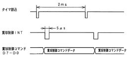
賞球制御コマンドは、主基板31から賞球制御基板37に、1バイト(8ビット:賞球制御コマンドD7〜D0)のデータとして出力される。また、賞球制御コマンドD7〜D0が出力されたときには、賞球制御INT信号が出力される。
【0131】
図6に示されたように、賞球制御コマンドは、出力ポート577を介して送信される。そして、この実施の形態では、図19に示すように、主基板31から賞球制御コマンドD7〜D0が出力されるときに、賞球制御INT信号が5μs以上ローレベルになる。賞球制御INT信号は、賞球制御基板37において、賞球制御用CPU371の割込端子に接続されている。よって、賞球制御用CPU371は、割り込みがあると、賞球制御コマンドD7〜D0が主基板31から送出されたことを認識でき、割込処理において賞球制御コマンド受信処理を行う。
【0132】
なお、図17に示されたコマンド構成は一例であって、他の構成にしてもよい。例えば、1バイト中の上位下位を、図17に示された構成とは逆にしてもよい。
【0133】
図20は、電源監視および電源バックアップのための賞球制御用CPU371周りの一構成例を示すブロック図である。図20に示すように、第1の電源監視回路(第1の電源監視手段)からの電圧低下信号が、バッファ回路960を介して賞球制御用CPU371のマスク不能割込端子(NMI端子)に接続されている。第1の電源監視回路は、遊技機が使用する各種直流電源のうちのいずれかの電源の電圧を監視して電源電圧低下を検出する回路である。この実施の形態では、VSLの電源電圧を監視して電圧値が所定値以下になるとローレベルの電圧低下信号を発生する。VSLは、遊技機で使用される直流電圧のうちで最大のものであり、この例では+30Vである。従って、賞球制御用CPU371は、割込処理によって電源断の発生を確認することができる
【0134】
賞球制御基板37には、初期リセット回路975も搭載されているが、この実施の形態では、初期リセット回路975は、第2の電源監視回路(第2の電源監視手段)も兼ねている。すなわち、リセットIC976は、電源投入時に、外付けのコンデンサに容量で決まる所定時間だけ出力をローレベルとし、所定時間が経過すると出力をハイレベルにする。また、リセットIC976は、電源基板910に搭載されている第1の電源監視回路が監視する電源電圧と等しい電源電圧であるVSLの電源電圧を監視して電圧値が所定値(例えば+9V)以下になるとローレベルの電圧低下信号を発生する。従って、電源断時には、リセットIC976からの電圧低下信号がローレベルになることによって賞球制御用CPU371がシステムリセットされる。なお、図20に示すように、電圧低下信号はリセット信号と同じ出力信号である。
【0135】
リセットIC976が電源断を検知するための所定値は、通常時の電圧より低いが、賞球制御用CPU371が暫くの間動作しうる程度の電圧である。また、リセットIC976が、賞球制御用CPU371が必要とする電圧(この例では+5V)よりも高い電圧を監視するように構成されているので、賞球制御用CPU371が必要とする電圧に対して監視範囲を広げることができる。従って、より精密な監視を行うことができる。
【0136】
+5V電源から電力が供給されていない間、賞球制御用CPU371の内蔵RAMの少なくとも一部は、電源基板から供給されるバックアップ電源がバックアップ端子に接続されることによってバックアップされ、遊技機に対する電源が断しても内容は保存される。そして、+5V電源が復旧すると、初期リセット回路975からリセット信号が発せられるので、賞球制御用CPU371は、通常の動作状態に復帰する。そのとき、必要なデータがバックアップされているので、停電等からの復旧時には停電発生時の遊技状態に復帰することができる。
【0137】
以上のように、この実施の形態では、電源基板910に搭載されている第1の電源監視回路が、遊技機で使用される直流電圧のうちで最も高い電源VSLの電圧を監視して、その電源の電圧が所定値を下回ったら電圧低下信号(電源断検出信号)を発生する。図10に示すように、電源断検出信号が出力されるタイミングでは、IC駆動電圧は、まだ各種回路素子を十分駆動できる電圧値になっている。従って、IC駆動電圧で動作する賞球制御基板37の賞球制御用CPU371が所定の電力供給停止時処理を行うための動作時間が確保されている。
【0138】
なお、ここでも、第1の電源監視回路は、遊技機で使用される直流電圧のうちで最も高い電源VSLの電圧を監視することになるが、電源断検出信号を発生するタイミングが、IC駆動電圧で動作する電気部品制御手段が所定の電力供給停止時処理を行うための動作時間が確保されるようなタイミングであれば、監視対象電圧は、最も高い電源VSLの電圧でなくてもよい。すなわち、少なくともIC駆動電圧よりも高い電圧を監視すれば、電気部品制御手段が所定の電力供給停止時処理を行うための動作時間が確保されるようなタイミングで電源断検出信号を発生することができる。
【0139】
その場合、上述したように、監視対象電圧は、賞球カウントスイッチ301A等の遊技機の各種スイッチに供給される電圧が+12Vであることから、電源断時のスイッチオン誤検出の防止も期待できる電圧であることが好ましい。すなわち、スイッチに供給される電圧(スイッチ電圧)である+12V電源電圧が落ち始める以前の段階で、電圧低下を検出できることが好ましい。よって、少なくともスイッチ電圧よりも高い電圧を監視することが好ましい。
【0140】
なお、図20に示された構成では、初期リセット回路975は、電源投入時に、コンデンサの容量で決まる期間のローレベルを出力し、その後ハイレベルを出力する。すなわち、リセット解除タイミングは1回だけである。しかし、図7に示された主基板31の場合と同様に、複数回のリセット解除タイミングが発生するような回路構成を用いてもよい。
【0141】
図21は、賞球制御用CPU371のメイン処理を示すフローチャートである。メイン処理では、賞球制御用CPU371は、まず、RAM領域をクリアする等の初期値設定処理を行う(ステップS701)。なお、内蔵RAMの電源バックアップされたRAM領域(バックアップ領域)にデータが設定されている場合には、それらの領域のクリア処理はなされない。その後、この実施の形態では、賞球制御用CPU371は、所定期間(例えば2ms)毎に発生するタイマ割込による割込処理で賞球払出制御を行う(ステップS702)。タイマ割込処理では、図22に示すように、賞球制御用CPU371は、賞球払出制御処理を実行する(ステップS711)。
【0142】
図23は、賞球制御用CPU371が内蔵するRAMの使用例を示す説明図である。この例では、バックアップRAM領域に総合個数記憶が(例えば2バイト)が形成されている。総合個数記憶は、主基板31の側から指示された払出個数の総数を記憶するものである。
【0143】
図24〜図30は、賞球制御用CPU371が実行する賞球払出制御処理を示すフローチャートである。なお、この実施の形態では、賞球払出制御処理はタイマ割込処理で実行されるように構成されているが、そのような構成ではなく、通常の処理(割込処理ではない)によって実行されるように構成してもよい。
【0144】
賞球払出制御処理において、賞球制御用CPU371は、賞球制御コマンドが受信されているか否か確認する(ステップS480)。受信されていれば、ステップS511に移行する。受信されていなければ、現在エラー状態中であるか否か確認する(ステップS481)。エラー状態中であればエラー処理を行う。エラー状態中でない場合には、賞球中(または補正払出中)であるか否か確認する(ステップS482)。賞球中でない場合には、玉貸し処理中であるか否か確認する(ステップS483)。玉貸し中であれば、玉貸し中の処理に移行する。
【0145】
玉貸し中でもなければ、総合個数記憶および補正個数カウンタの値が0であるか否か確認する(ステップS484)。それらが0であれば、すなわち、賞球払出を行う必要がない場合には、遊技機の外部機器としてのカードユニット50からの玉貸し要求信号であるBRQ信号がオンになっているかどうか確認する(ステップS491)。なお、補正個数カウンタとは、払出個数不足が検出されたときに不足分を補正個数として払い出すように構成された場合に、補正個数が設定されるカウンタである。そのような補正制御を行わない場合には使用されない。
【0146】
BRQ信号がオンになっていれば、玉貸し開始のための処理を行って(ステップS492)、玉貸し中の処理に移行する。なお、玉貸し制御のためのカウンタも、バックアップRAM領域に形成されていることが好ましい。
【0147】
ステップS484において、総合個数記憶および補正個数カウンタの値が全て0になっていなければ、ステップS500の処理を行う。
【0148】
ステップS500において、補正払出フラグがオンしていれば、すなわち、補正払出をすべきことに決定されていた場合には、ステップS507に移行する。補正払出フラグがオンしていなければ、賞球制御用CPU371は、賞球処理中フラグをオンし(ステップS503)、払出モータ289をオンする(ステップS507)。そして、賞球払出中処理に移行する。
【0149】
賞球制御コマンド(払出個数指示コマンド)を受信した場合には、ステップS511の処理が開始される。ステップS511において、賞球制御用CPU371は、払出個数指示コマンドで指示された個数を総合個数記憶に加算する(ステップS512)。
【0150】
以上のように、賞球制御基板37に搭載された賞球制御用CPU371は、主基板31のCPU56から送られた払出個数指示コマンドに含まれる賞球数をバックアップRAM領域(総合個数記憶)に記憶する。
【0151】
なお、賞球制御コマンドには払出個数指示コマンド以外のコマンドもあるが、図26では、それらのコマンドの受信処理は省略されている。
【0152】
図27に示すステップS532以降の処理は賞球払出中の処理である。賞球払出中の処理において、まず、状態チェックが行われる(ステップS532)。賞球制御用CPU371は、払出モータ位置センサおよび賞球カウントスイッチ301Aを監視することによって賞球払出が正常に行われているか否かチェックする。状態チェックとは、現在、払出モータ位置センサのオンを監視している状態にあるのか、払出モータ位置センサのオフを監視している状態にあるのかを判定する処理である。
【0153】
この実施の形態では、払出モータ位置センサおよび賞球カウントスイッチ301Aの監視のために、以下のタイマを用いる。
(1)タイマT11:払出モータ位置センサのオン監視用
(2)タイマT12:払出モータ位置センサのオフ監視用
(3)タイマT13:賞球カウントスイッチ301Aのオン監視用
(4)タイマT14:賞球カウントスイッチ301Aのオフ監視用
【0154】
また、払出モータ位置センサによって払出個数が確認されてから、賞球カウントスイッチ301Aが実際の払出球を検出するまでに遊技球数個分の流下に要する遅れ時間があり、その時間を待つために以下のタイマを用いる。
(5)タイマT15:最後の払出球が払出モータ位置センサによって確認されてから、その球が賞球カウントスイッチ301Aを通過するまでの時間待ち用
【0155】
ここでは、それらのタイマが動作中であることを確認することによって状態チェックを行う。ステップS532では、タイマT11が動作中であるときには、払出モータ位置センサのオン待ち処理(ステップS534)に移行し、タイマT12が動作中であるときには、払出モータ位置センサのオフ待ち処理(ステップS542)に移行する。タイマ15が動作中であるときには、タイマ15のタイムアウト待ち(ステップS573)に移行する。いずれのタイマも動作中でないときには、タイマT11をスタートさせる(ステップS533)。
【0156】
ステップS534において、賞球制御用CPU371は、払出モータ位置センサがオンするのを待つ。オンする前にタイマT11がタイムアウトするとエラー処理に移行する(ステップS535,S536)。払出モータ位置センサがオンすると、タイマT11を停止して(ステップS537)、タイマT12を起動する(ステップS541)。その後、賞球制御用CPU371は、払出モータ位置センサがオフするのを待つ(ステップS542)。オフする前にタイマT12がタイムアウトするとエラー処理に移行する(ステップS543,S545)。なお、タイマT11,T12がタイムアウトしていない間、賞球カウントスイッチチェックサブルーチンを実行する(ステップS547)。
【0157】
払出モータ位置センサがオフすると、タイマT12を停止して(ステップS546)、補正払出中でなければ(ステップS549)、払出カウンタを+1するとともに(ステップS550)、総合個数記憶を−1する(ステップS551)。そして、総合個数記憶の値が0になったら(ステップS552)、ステップS571に移行する。補正払出中であれば、補正個数カウンタの値を−1し(ステップS560)、補正個数カウンタの値が0になったら(ステップS561)、ステップS571に移行する。ステップS571では、払出モータ289の駆動が停止される。また、タイマT15が起動される(ステップS572)。
【0158】
その後、タイマT15のタイムアウトを待つ(ステップS573)。タイムアウトしていない間、賞球カウントスイッチチェックサブルーチンを実行する(ステップS576)。
【0159】
タイマT15がタイムアウトすると、補正払出中でなければ(ステップS574)、払出カウンタの値とと賞球数カウンタの値を比較する(ステップS575)。
【0160】
なお、賞球数カウンタは、賞球カウントスイッチチェックサブルーチンで、払出モータ位置センサの下部に位置する賞球カウントスイッチ301Aの1回のオンが検出される度にカウントアップされる。タイマT15がタイムアウトしたとき、玉払出が正常に行われていれば、賞球数カウンタの値は、払出モータ位置センサのオン回数に一致する。例えば、n個賞球が行われていたときには、払出モータ位置センサのオン回数がnになると、ステップS552で総合個数記憶の値が0になり、その後、T15の時間だけ経過すると賞球数カウンタの値がnになるはずである。
【0161】
ステップS575の判断結果が不一致の場合には、賞球不足数(賞球予定数−賞球数カウンタ値)を払出個数カウンタに設定し(ステップS583)、払出モータ289をオンし(ステップS584)、補正払出中フラグをオンする(ステップS585)。その後に、補正払出を開始した旨を示す報知(例えばブザー報知)を例えば20秒間行う(ステップS586)。この報知は、遊技店員に賞球装置の異常があるかもしれないことを知らせる目的で行われるとともに、賞球カウントスイッチ301Aの故障または引き抜き(不正)の可能性を示唆するために行われる。なお、賞球不足数は補正予定数として記憶される。
【0162】
補正払出が行われていた場合には、賞球数カウンタの値が補正予定数と一致しているか否か確認し(ステップS581)、一致していなければ、ステップS586に移行する。一致していれば、補正払出中フラグをリセットして(ステップS582)、この回の処理を終了する。
【0163】
ステップS575の判断結果が一致であった場合には、賞球処理中フラグをリセットして(ステップS587)、処理を終了する。
【0164】
以上のように、賞球制御用CPU371は、総合記憶個数の値によって、賞球が完了したか否か認識し、完了したら、所定時間経過後に賞球カウントスイッチ301Aによる検出回数を確認し、賞球カウントスイッチ301Aを通過した遊技球数が予定払出数に満たないことを検出した場合には補正払出処理を開始する。
【0165】
なお、総合記憶個数はバックアップRAM領域に形成されているので、停電等による電源断が生じても保存される。よって、停電等からの復旧時に、賞球制御用CPU371は、保存されているデータにもとづいて賞球払出制御を継続することができる。例えば、停電からの復旧時に、総合記憶個数が設定されていることを検知して、賞球制御用CPU371は、賞球払出処理を再開することができる。
【0166】
さらに、補正個数カウンタ等もバックアップRAM領域に形成すれば、補正払出処理中に停電等が生じても、停電等からの復旧時に、賞球制御用CPU371は、保存されているデータにもとづいて補正払出制御を継続することができる。
【0167】
図30は、賞球カウントスイッチチェックサブルーチンを示すフローチャートである。賞球カウントスイッチチェックにおいて、まず、状態チェックが行われる(ステップS511)。ステップS511において、タイマT13が動作中であるときには、賞球カウントスイッチ301Aのオン待ち処理(ステップS513)に移行し、タイマT14が動作中であるときには、賞球カウントスイッチ301Aのオフ待ち処理(ステップS518)に移行する。いずれのタイマも動作中でないときには、タイマT13をスタートさせる(ステップS512)。
【0168】
そして、賞球カウントスイッチ301Aがオンするのを待つ(ステップS513)。賞球カウントスイッチ301Aの出力がオンする前にタイマT13がタイムアウトするとエラー処理に移行する(ステップS514,S515)。
【0169】
賞球カウントスイッチ301Aの出力がオン状態になると、タイマT13を停止して(ステップS516)、タイマT14を起動する(ステップS517)。そして、賞球カウントスイッチ301Aがオフするのを待つ(ステップS518)。賞球カウントスイッチ301Aがオフする前にタイマT14がタイムアウトするとエラー処理に移行する(ステップS519,S520)。タイマT14がタイムアウトする前に賞球カウントスイッチ301Aがオフした場合には、タイマT14を停止する(ステップS521)。そして、賞球数カウンタの値を+1する(ステップS522)。
【0170】
なお、この実施の形態では、遊技制御手段から賞球指示を受けると、総合個数記憶に賞球数を加算して、総合個数記憶の値を用いて払出制御を行ったが、遊技制御手段からの賞球指示に対して、賞球対応に設けられた個数カウンタに賞球回数を記憶するようにしてもよい。
【0171】
図31は、賞球制御用CPU371が第1の電源監視手段からの割込に応じて実行される停電発生割込処理を示すフローチャートである。電源基板910の電源監視用IC902が電源電圧の低下を検出すると電圧低下信号が電圧低下を示す状態となり、停電発生割込処理が開始される。停電発生割込処理において、賞球制御用CPU371は、割込禁止に設定し(ステップS801)、RAMアクセス禁止状態に設定して(ステップS802)、ループ処理に入る。すなわち、何らの処理もしない状態になる。
【0172】
従って、図20に示されたリセットIC976からのリセット信号によって外部から動作禁止状態(システムリセット)にされる前に、内部的に動作停止状態になる。よって、電源断時に確実に賞球制御用CPU371は動作停止する。その結果、電源電圧が低下していくことに伴って生ずる可能性がある異常動作に起因するRAMの内容破壊等を確実に防止することができる。
【0173】
なお、図31に示された処理は電力供給停止時処理の一例である。また、この実施の形態では、停電発生NMI処理では最終部でプログラムをループ状態にしたが、ホールト(HALT)命令を発行するように構成してもよい。また、割込処理中には他の割込がかからないような仕様のCPUを用いた場合にはステップS801の処理は不要である。
【0174】
図32は、賞球制御用CPU371が電源投入時に実行する初期化処理(ステップS701)の一部を示すフローチャートである。電源が投入され、または、電源が復旧したときには、賞球制御用CPU371は、まず、バックアップRAM領域に形成されている総合個数記憶または貸し玉個数記憶の値が0でないかどうか確認する(ステップS901)。0である場合には、前回の電源オフ時に未払出賞球はなかったことになるので、通常の初期設定処理を行う。すなわち、レジスタおよび全RAM領域をクリアして(ステップS903)、スタックポインタの初期設定を行う(ステップS904)。なお、貸し玉個数記憶とは、貸し玉個数についてもバックアップRAMに保存するように構成した場合に、バックアップRAMに形成される記憶領域である。また、上述した補正払出制御を行う場合には、ステップS901において、バックアップRAMに形成されている補正個数カウンタの値を確認するようにしてもよい。
【0175】
総合個数記憶または貸し玉個数記憶の値が0でない場合には、アドレスを指定してレジスタと非バックアップRAM領域をクリアする(ステップS905)。そして、賞球再開のための設定を行う。例えば、賞球中処理中フラグのセット等を行う(ステップS906)。なお、バックアップRAM領域であっても、賞球個数に関わらない領域であるならば、それらのアドレスを指定してクリアするようにしてもよい。
【0176】
このように、賞球制御用CPU371は、電源投入時に、バックアップRAM領域のデータを確認するだけで、通常の初期設定処理を行うのか賞球中の状態を復元するのか決定できる。すなわち、簡単な判断によって、未払出賞球について賞球処理再開を行うことができる。
【0177】
図32に示された処理では、賞球制御用CPU371は、電源投入時に、バックアップRAM領域のデータを確認したが、そのような判断を行わなくてもよい。すなわち、図33に示すように、電源投入時に、電源バックアップされていないRAM領域のみをアドレスを指定してクリアする(ステップS910)。なお、ここで、レジスタのクリア処理も行う。
【0178】
そして、上記の初期化処理を行うように構成されている場合、電源断時に、レジスタの退避は行われない。
【0179】
なお、賞球制御用CPU371も、主基板31のCPU56と同様に、電源断フラグによって初期化処理を行うか否か決定してもよい。また、主基板31のCPU56と同様に、パリティチェックコードによって記憶内容保存の確実化を図ってもよい。
【0180】
また、この実施の形態では、賞球制御用CPU371は、マスク不能外部割込端子(NMI端子)を介して電源基板からの第1の電圧低下信号(第1の電源監視手段からの電圧低下信号)を検知したが、第1の電圧低下信号をマスク可能割込割込端子(IRQ端子)に導入してもよい。その場合には、IRQ処理によって図27に示された停電発生割込処理が実行される。また、入力ポートを介して第1の電圧低下信号を検知してもよい。その場合には、賞球制御用CPU371が実行するメイン処理において、入力ポートの監視が行われる。
【0181】
なお、上記の各実施の形態では、主基板31のCPU56および賞球制御基板37の賞球制御用CPU371について割込による電力供給停止時処理を説明したが、他の各基板(表示制御基板80、音声制御基板70およびランプ制御基板35)に搭載されているCPUも、割込による電力供給停止時処理を行ってもよい。その際、電圧低下を示す信号は、マスク可能な外部割込端子に接続されていてもよいし、NMI端子に接続されていてもよい。
【0182】
また、遊技制御手段および賞球制御手段におけるRAMと同様に、音声制御手段、ランプ制御手段および表示制御手段におけるRAMも、電源バックアップされる部分があるようにしてもよい。
【0183】
また、上記の実施の形態では、第1の電源監視手段は電源基板910に設けられ、第2の電源監視手段は電気部品制御基板に設けられたが、第1の電源監視手段および第2の電源監視手段がともに電気部品制御基板に設けられていてもよい。
【0184】
【発明の効果】
以上のように、本発明によれば、遊技機を、遊技機に設けられる電気部品を制御するための処理を行う電気部品制御マイクロコンピュータと、遊技機で使用される所定電位電源を監視し検出条件が成立したことにより検出信号を電気部品制御マイクロコンピュータに出力する電源監視手段と、交流電流を整流する整流手段と、整流手段によって整流された後の電圧を降圧し、電気部品制御マイクロコンピュータおよび電気部品が使用する電圧を生成する降圧電圧生成手段とを備え、電気部品制御マイクロコンピュータが、電源監視手段からの検出信号により電源断フラグの設定およびRAMアクセス禁止処理を含む所定の電力供給停止時処理を行い、電源監視手段は、監視する所定電位電源として、整流手段によって整流された後、降圧電圧生成手段によって降圧される前の電圧の電源を監視し、電気部品制御マイクロコンピュータは降圧電圧生成手段が降圧することによって生成した電圧であって遊技球を検出するためのスイッチに供給される電圧よりも低い電圧の電源により動作し、電気部品制御マイクロコンピュータは、遊技媒体の払出制御を行う払出制御用マイクロコンピュータを含み、電力供給開始時に電源断フラグが設定されていることを条件にRAMのバックアップ領域のデータチェックを行い、チェック結果が正常のときは、電源断フラグのみクリアし、チェック結果が正常でないときは、初期化処理で電源断フラグが設定されている領域を含むRAMの領域をクリアする処理を行い、少なくとも払出個数に関わる情報は払出制御用マイクロコンピュータのRAMのバックアップ領域に記憶され、払出制御用マイクロコンピュータは、電力供給開始時の初期化処理で、少なくともRAMのバックアップされていない領域をクリアする処理を行うように構成したので、停電等による不測の電源断が発生しても、そのことを確実に検出できる効果がある。特に、所定電位電源が整流手段によって整流された後、降圧電圧生成手段によって降圧される前の電圧であって遊技球を検出するためのスイッチに供給される電圧よりも高い電圧の電源であることから、電圧監視範囲を広げることができ、電気部品制御マイクロコンピュータが所定の電力供給停止時処理を確実に完了できるようなタイミングで電源監視手段から検出信号が発生される。また、初期化処理が簡単でよいという効果もある。
【0193】
払出制御用マイクロコンピュータが、電力供給開始時の初期化処理で、バックアップ領域に払出個数に関わる情報が記憶されていた場合には、RAMの少なくともバックアップされていない領域をクリアする処理を行うとともに前記情報にもとづいて払出制御を行い、バックアップ領域に賞球個数に関わる情報が記憶されていない場合にはRAMの全領域を初期化するように構成されている場合には、バックアップ記憶手段領域のデータを確認するだけで、通常の初期設定処理を行うのか払出制御中の状態を復元するのか決定できるので、簡単な判断によって未払出個数について払出処理再開を行うことができる状態になる。
【図面の簡単な説明】
【図1】 パチンコ遊技機を正面からみた正面図である。
【図2】 パチンコ遊技機の遊技盤を正面からみた正面図である。
【図3】 パチンコ遊技機を背面からみた背面図である。
【図4】 遊技制御基板(主基板)の回路構成例を示すブロック図である。
【図5】 表示制御基板の回路構成例を示すブロック図である。
【図6】 賞球制御基板の回路構成例を示すブロック図である。
【図7】 電源監視および電源バックアップのためのCPU周りの一構成例を示すブロック図である。
【図8】 電源基板の一構成例を示すブロック図である。
【図9】 電源投入時のリセット信号の様子を示すタイミング図である。
【図10】 遊技機の電源断時の電源低下やNMI信号の様子を示すタイミング図である。
【図11】 主基板におけるメイン動作を示すフローチャートである。
【図12】 主基板のCPUが実行する初期化処理を示すフローチャートである。
【図13】 2msタイマ割込処理を示すフローチャートである。
【図14】 遊技制御処理を示すフローチャートである。
【図15】 電源断時の割込処理を示すフローチャートである。
【図16】 バックアップパリティデータ作成方法を説明するための説明図である。
【図17】 賞球制御コマンドの構成例を示す説明図である。
【図18】 賞球制御コマンドのビット構成を示す説明図である。
【図19】 賞球制御コマンドデータの出力の様子を示すタイミング図である。
【図20】 電源監視および電源バックアップのための賞球制御用CPU周りの一構成例を示すブロック図である。
【図21】 賞球制御用CPUが実行するメイン処理を示すフローチャートである。
【図22】 賞球制御用CPUの2msタイマ割込処理を示すフローチャートである。
【図23】 賞球制御手段におけるRAMの一構成例を示す説明図である。
【図24】 賞球制御用CPUの賞球制御処理を示すフローチャートである。
【図25】 賞球制御用CPUの賞球制御処理を示すフローチャートである。
【図26】 賞球制御用CPUの賞球制御処理を示すフローチャートである。
【図27】 賞球制御用CPUの賞球制御処理を示すフローチャートである。
【図28】 賞球制御用CPUの賞球制御処理を示すフローチャートである。
【図29】 賞球制御用CPUの賞球制御処理を示すフローチャートである。
【図30】 賞球制御用CPUの賞球制御処理を示すフローチャートである。
【図31】 賞球制御用のNMI割込処理を示すフローチャートである。
【図32】 賞球制御用CPUが実行する初期化処理処理を示すフローチャートである。
【図33】 賞球制御用CPUが実行する初期化処理処理の他の例を示すフローチャートである。
【符号の説明】
1 パチンコ遊技機
31 主基板
37 賞球制御基板
53 基本回路
56 CPU
65 初期リセット回路
651 リセットIC
902 電源監視用IC
910 電源基板
916 コンデンサ[0001]
BACKGROUND OF THE INVENTION
The present invention relates to a gaming machine such as a pachinko gaming machine, a coin gaming machine, or a slot machine in which a game is performed according to a player's operation, and particularly, a game is performed according to a player's operation in a gaming area on a gaming board. It relates to gaming machines.
[0002]
[Prior art]
As a gaming machine, a game medium such as a game ball is launched into a game area by a launching device, and when a game medium wins a prize area such as a prize opening provided in the game area, a predetermined number of prize balls are paid out to the player. There is something to be done. Further, a variable display unit capable of changing the display state is provided, and is configured to give a predetermined game value to the player when the display result of the variable display unit becomes a predetermined specific display mode There is.
[0003]
Note that the game value is the right that the state of the variable winning ball device provided in the gaming area of the gaming machine is advantageous for a player who is likely to win a ball, or the advantageous state for a player. Or a condition that a condition for paying out premium game media is likely to be satisfied.
[0004]
In a pachinko game machine, the combination of a specific display mode with a predetermined display result of a variable display unit that displays special symbols is usually referred to as “big hit”. When a big hit occurs, for example, the big winning opening is opened a predetermined number of times, and the game shifts to a big hit gaming state in which a hit ball is easy to win. And in each open period, if there is a prize for a predetermined number (for example, 10) of the big prize opening, the big prize opening is closed. And the number of times the special winning opening is opened is fixed to a predetermined number (for example, 16 rounds). Note that an opening time (for example, 29.5 seconds) is determined for each opening, and even if the number of winnings does not reach a predetermined number, the big winning opening is closed when the opening time elapses. Further, when a predetermined condition (for example, winning in the V zone provided in the big prize opening) is not established at the time when the big prize opening is closed, the big hit gaming state is ended.
[0005]
In addition, among the combinations of display modes other than the “big hit” combination, the variable display in which the display result has already been derived and displayed at the stage where some of the display results of the plurality of variable display units have not yet been derived and displayed. A state in which the display mode of the part satisfies a display condition that is a combination of specific display modes is referred to as “reach”. Then, if the display result of the identification information variably displayed on the variable display portion does not satisfy the condition of “reach”, it becomes “missing”, and the variable display state ends. A player plays a game while enjoying how to generate a big hit.
[0006]
The game progress in the gaming machine is controlled by game control means such as a microcomputer. The identification information, character image, and background image displayed on the variable display device are controlled by display control means that operates in accordance with display control command data from the game control means. In general, the identification information, character image, and background image displayed on the variable display device are a display control microcomputer and a video display processor that generates image data in accordance with instructions from the microcomputer and transfers the image data to the variable display device side ( VDP), the program capacity of the display control microcomputer is large.
[0007]
Therefore, it is impossible to control identification information and the like displayed on the variable display device by the microcomputer of the game control means having a limited program capacity, and the display control microcomputer (separate from the microcomputer of the game control means) Display control means) is used. Therefore, the game control means for controlling the progress of the game needs to transmit a display control command to the display control means.
[0008]
In such a gaming machine, a speaker is provided on the game board, and various sound effects are emitted from the speaker as the game progresses in order to enhance the gaming effect. In addition, light emitters such as lamps and LEDs are provided on the game board, and these light emitters are turned on and off as the game progresses in order to enhance the gaming effect. In general, sound control for generating sound effects and lamp lighting / extinguishing timing control are performed by game control means for controlling the progress of the game. Therefore, it is necessary for the game control means to transmit a command to the sound control means or the lamp control means for actually generating sound or driving the lamp / LED.
[0009]
Since the progress of the game is controlled by game control means mounted on the main board, the number of winning balls based on winning is determined by the game control means and transmitted to the winning ball control board. On the other hand, the rental of game media is irrelevant to the progress of the game, and is generally controlled by the prize ball control means without going through the game control means.
[0010]
As described above, various control means are mounted on the gaming machine in addition to the game control means. Then, the game control means for controlling the progress of the game transmits each command indicating an operation instruction according to the game situation to each control means mounted on each control board.
[0011]
[Problems to be solved by the invention]
Generally, each control means is constituted by a microcomputer. That is, a program is stored in a ROM or the like, and data temporarily generated for control or data that changes as control proceeds is stored in the RAM. Then, when the power-off state due to a power failure or the like occurs in the gaming machine, the data in the RAM is lost. Therefore, when recovering from a power outage or the like, the player must return to the initial state (for example, the state when the game machine was first turned on at the game store for the first time in the day), which may cause a disadvantage to the player. There is. For example, if a power failure occurs during a jackpot game and the gaming machine returns to the initial state, the player cannot enjoy the benefits based on the jackpot.
[0012]
Therefore, an object of the present invention is to provide a gaming machine that can prevent a player from being disadvantaged as much as possible even when a power interruption occurs.
[0013]
[Means for Solving the Problems]
A gaming machine according to the present invention is a gaming machine capable of performing a predetermined game using a game ball, and is provided with a RAM capable of holding stored contents for a predetermined period even when power supply is stopped. An electric component control microcomputer that performs processing for controlling the electric component to be controlled, and a power supply monitor that monitors a predetermined potential power source used in the gaming machine and outputs a detection signal to the electric component control microcomputer when a detection condition is satisfied An electric component, and a rectifying unit that rectifies an alternating current; a step-down voltage generating unit that steps down a voltage rectified by the rectifying unit and generates a voltage used by the electric component control microcomputer and the electric component; The control microcomputer uses a detection signal from the power supply monitoring means.Set the power-off flag andA predetermined power supply stop process including a RAM access prohibition process is performed, and the power supply monitoring unit is a voltage before being stepped down by the step-down voltage generation unit after being rectified by the rectification unit as a predetermined potential power source to be monitored. The power supply of a voltage higher than the voltage supplied to the switch for detecting the game ball is monitored, and the electric component control microcomputer detects the game ball, which is a voltage generated by the step-down voltage generation means stepping down. Operated by a power supply with a voltage lower than the voltage supplied to the switch forThe electronic component control microcomputer includes a payout control microcomputer that performs payout control of the game medium, and performs data check in the backup area of the RAM on the condition that the power-off flag is set at the start of power supply. When the check result is normal, only the power-off flag is cleared. When the check result is not normal, the RAM area including the area where the power-off flag is set in the initialization process is cleared and at least paid out. Information related to the number is stored in a RAM backup area of the payout control microcomputer, and the payout control microcomputer performs an initialization process at the start of power supply, and at least clears an unbacked area in the RAM.It is characterized by that.
[0021]
Dispensing controlforIn the initialization process at the start of power supply, the microcomputer stores information related to the number of payouts in the backup area.RAMAt leastBaWhen clearing the area that is not backed up and performing payout control based on the above information, if the information related to the number of prize balls is not stored in the backup areaRAMThe entire area may be initialized.
[0022]
DETAILED DESCRIPTION OF THE INVENTION
Hereinafter, an embodiment of the present invention will be described with reference to the drawings.
First, an overall configuration of a pachinko gaming machine that is an example of a gaming machine will be described. 1 is a front view of the
[0023]
As shown in FIG. 1, the
[0024]
Near the center of the
[0025]
An open / close plate 20 that is opened by a
[0026]
The
[0027]
In this example, a
[0028]
The
[0029]
The hit ball fired from the hit ball launching device enters the
[0030]
The rotation of the image in the
[0031]
When the combination of images in the
[0032]
Next, the structure of the back surface of the
On the back surface of the
[0033]
The
[0034]
FIG. 3 is a rear view of the mechanism plate of the
[0035]
In order to perform prize ball payout control, signals from the prize opening switches 19 a and 24 a, the start opening switch 17 and the
[0036]
FIG. 4 is a block diagram illustrating an example of a circuit configuration in the
[0037]
Further, according to the data given from the basic circuit 53, the jackpot information indicating the occurrence of the jackpot, the effective starting information indicating the number of starting winning balls used for starting the image display of the
[0038]
The basic circuit 53 includes a ROM 54 that stores a game control program and the like, a RAM 55 that is an example of storage means used as a work memory, a
[0039]
Further, the
Note that there is also switch information input to the
[0040]
A ball hitting device for hitting and launching a game ball is driven by a drive motor 94 controlled by a circuit on the
[0041]
FIG. 5 is a block diagram showing a circuit configuration in the
[0042]
The display control CPU 101 operates in accordance with a program stored in the
[0043]
Then, the display control CPU 101 performs display control of the screen displayed on the
[0044]
5 also shows a
[0045]
FIG. 6 is a block diagram showing components related to the prize ball, such as the components of the prize
[0046]
A detection signal from the ball break switch 187 (187a, 187b) is input to the I /
[0047]
The
[0048]
Further, a detection signal from the prize ball count switch 301 </ b> A is also input to the I /
[0049]
When there is a prize, a prize ball control command indicating the number of prize balls is input to the prize
[0050]
Further, the prize
[0051]
Further, the detection signal of the prize
[0052]
The
[0053]
A ball lending switch signal and a return switch signal are given from the balance display board 74 to the
[0054]
When the power of the
[0055]
As described above, all signals from the
[0056]
In this embodiment, at least the
[0057]
FIG. 7 is a block diagram showing a configuration example around the
[0058]
Although an initial reset circuit 65 is also shown on the electrical component control board, in this embodiment, the initial reset circuit 65 also serves as a second power supply monitoring circuit (second power supply monitoring means). That is, when the power is turned on, the
[0059]
As shown in FIG. 7, the reset signal from the
[0060]
For example, the detection voltage of the first power supply monitoring circuit (voltage that outputs a voltage drop signal) is set to + 22V, and the detection voltage of the second power supply monitoring circuit is set to + 9V. In such a configuration, since the first power monitoring circuit and the second power monitoring circuit monitor the voltage of the same power supply VSL, the timing when the first voltage monitoring circuit outputs the voltage drop signal. And the timing at which the second voltage monitoring circuit outputs the voltage drop signal can be reliably set to a desired predetermined period. The desired predetermined period is a period from when the power supply stop process is started in response to the voltage drop signal from the first power supply monitoring circuit until the power supply stop process is reliably completed.
[0061]
In this example, the first detection condition for the first power supply monitoring means to output the detection signal is that the + 30V power supply voltage has dropped to + 22V, and the second power supply monitoring means outputs the detection signal. The second detection condition that becomes is that the + 30V power supply voltage is lowered to + 9V. However, the voltage value used here is an example, and other values may be used.
[0062]
However, although the monitoring range is narrowed, it is also possible to use a + 5V power supply voltage as the monitoring voltage of the first voltage monitoring circuit and the second voltage monitoring circuit. Even in this case, the detection potential of the first voltage monitoring circuit is set higher than the detection potential of the second voltage monitoring circuit.
[0063]
While power is not supplied from the + 5V power source that is the driving power source of the
[0064]
FIG. 8 is a block diagram illustrating a configuration example of the power supply board 910 of the gaming machine. The power supply board 910 is installed independently of electrical component control boards such as the
[0065]
The transformer 911 converts AC voltage from the AC power source into 24V. The AC 24V voltage is output to the connector 915. The rectifier circuit 912 also generates a DC voltage of +30 V from AC 24 V and outputs it to the DC-DC converter 913 and the connector 915. The DC-DC converter 913 generates + 21V, + 12V, and + 5V and outputs them to the connector 915. The connector 915 is connected to, for example, a relay board, and power of a voltage necessary for each electric component control board and the mechanism component is supplied from the relay board. Note that a
[0066]
The + 5V line from the DC-DC converter 913 branches to form a backup + 5V line. A large-
[0067]
A battery that can be charged from a + 5V power supply may be used as the backup power supply. In the case of using a battery, a rechargeable battery is used in which the capacity disappears when a state in which no power is supplied from the +5 V power source continues for a predetermined time.
[0068]
The power supply board 910 is mounted with a
[0069]
The predetermined value for the
[0070]
Further, since the
[0071]
In the configuration shown in FIG. 8, the detection output (voltage drop signal) of the power
[0072]
FIG. 9 is a timing chart showing states of output signals of the
[0073]
When the
[0074]
Therefore, when the gaming machine is turned on, a signal is supplied to the reset terminal of the
[0075]
Note that the widths of the high level pulse (corresponding to the reset release state) and the low level pulse (corresponding to the reset state) output from the
[0076]
When the reset state is released and the operation is started, the
[0077]
Further, when the power is cut off, if the potential of VSL (+30 V power supply voltage in this example) input to the
[0078]
In this embodiment, the circuit configuration as shown in FIG. 7 is used in order to create the signal state as shown in the lowermost part of FIG. 9, but in order to create such a signal state. Other circuit configurations may be used.
[0079]
In addition, when using the
[0080]
FIG. 10 is a timing chart showing the state of power supply reduction and NMI signal (= power supply cut-off signal: first voltage drop signal) when the gaming machine is turned off. When the power supply to the gaming machine is cut off, the voltage value of VSL, which is the highest DC power supply voltage, gradually decreases. In this example, when the voltage drops to +22 V, a power cut-off signal (voltage drop signal) is output from the
[0081]
The power-off signal is introduced into the electrical component control board (in this embodiment, the
[0082]
When the voltage value of VSL further decreases to a predetermined value (+9 V in this example), the output of the
[0083]
When the voltage value of VSL is further decreased to be lower than a voltage capable of generating Vcc (+5 V for driving various circuits), each circuit cannot be operated on each substrate. However, at least the
[0084]
As described above, in this embodiment, the first power supply monitoring circuit monitors the voltage of the highest power supply VSL among the DC voltages used in the gaming machine, and the power supply voltage falls below a predetermined value. Then, a voltage drop signal (power-off detection signal) is generated. As shown in FIG. 10, at the timing when the power-off detection signal is output, the IC drive voltage is still a voltage value that can sufficiently drive various circuit elements. Therefore, an operation time is ensured for the
[0085]
In this case, the first power supply monitoring circuit monitors the voltage of the highest power supply VSL among the DC voltages used in the gaming machine, but the timing of generating the power-off detection signal is operated by the IC drive voltage. The monitoring target voltage may not be the highest voltage of the power supply VSL as long as the operation time for the electrical component control means to perform a predetermined power supply stop process is ensured. That is, if at least a voltage higher than the IC drive voltage is monitored, the power-off detection signal may be generated at such a timing that the operation time for the electric component control means to perform the predetermined power supply stop process is ensured. it can.
[0086]
In this case, as described above, the voltage to be monitored is preferably a voltage that can be expected to prevent erroneous switch-on detection when the power is cut off because the voltage supplied to the various switches of the gaming machine is + 12V. That is, it is preferable that the voltage drop can be detected before the +12 V power supply voltage, which is the voltage supplied to the switch (switch voltage) starts to drop. Therefore, it is preferable to monitor a voltage higher than at least the switch voltage.
[0087]
Hereinafter, the control operation of the gaming machine will be described.
FIG. 11 is a flowchart showing main processing executed by the
[0088]
If it is time to recover from a power failure, a data check (parity check in this example) of the backup RAM area is performed (step S3). In the case of recovery after an unexpected power failure, the data in the backup RAM area should have been saved, so the check result is normal. If the check result is not normal, the internal state cannot be returned to the state when the power is cut off, and therefore an initialization process that is executed when the power is turned on not when the power failure is restored is executed (steps S4 and S2).
[0089]
If the check result is normal, the
[0090]
If it is not time to recover from a power failure, the
[0091]
Here, it is confirmed in step S1 whether or not the recovery from the power failure, and if the recovery from the power failure, the parity check is performed. First, the parity check is performed and the check result is not normal. If it is determined that the power is not recovered from the power failure, the initialization process of step S2 is executed. If the check result is normal, the game state return process may be performed. That is, it may be determined whether or not recovery from a power failure is made based on the result of the parity check.
[0092]
Further, when determining whether or not to execute the power failure recovery processing, that is, when determining whether or not to restore the gaming state, according to the special process flag or the like in the stored RAM data or the start winning memory number data, If it is confirmed that the gaming machine is in a game standby state (not changing in design, not in big hit game, not in probable change, and no start winning memory), it is initial without performing game state recovery processing. The process may be executed.
[0093]
In the normal initialization process, as shown in FIG. 12, after the register and RAM clear process (step S2a) and the necessary initial value setting process (step S2b) are performed, a timer allocation is periodically performed every 2 ms. Initial setting of the timer register provided in the CPU 56 (setting that the time-out is 2 ms and the timer repeatedly operates) is performed so as to cause a delay (step S2c). That is, in step S2c, processing for activating a timer interrupt and processing for setting a timer interrupt interval are executed.
[0094]
Therefore, in this embodiment, the internal timer of the
[0095]
When detecting that the timer interrupt flag is set in step S8, the
[0096]
FIG. 14 is a flowchart showing the game control process of step S10. In the game control process, the
[0097]
Next, a process of outputting the contents of the storage area for various output data to each output port is performed (data output process: step S23). Also, output data setting processing is performed for setting output data such as jackpot information, start information, probability variation information, etc., output to the hall management computer in the storage area (step S24). Further, various abnormality diagnosis processes are performed by the self-diagnosis function provided in the
[0098]
Next, a process of updating each counter indicating each determination random number such as a big hit determination random number used for game control is performed (step S26).
[0099]
Further, the
[0100]
Further, the
[0101]
Further, the
[0102]
As described above, the main process includes a process for determining whether or not to shift to the game control process, and the timer control process based on the timer interrupt periodically generated by the internal timer of the
[0103]
Conventional general game control processing is forcibly returned to the initial state by an external interrupt that occurs periodically. If it demonstrates in accordance with the example shown by FIG. 14, for example, even if it was during the process of step S31, it was forcibly returned to the process of step S21. In other words, there is a possibility that the next game control process will be started before all the processes in the game control process are completed.
[0104]
Here, the game control process executed by the
[0105]
Even in such a configuration, the determination of the flag is not performed until all of the game control processes are executed, so that it is guaranteed that all the processes in the game control process are completed.
[0106]
FIG. 15 is a flowchart showing an example of a power failure occurrence NMI process executed in response to the NMI based on the voltage drop signal from the first power supply monitoring circuit of the power supply board 910. In the power failure occurrence NMI process, the
[0107]
Note that the processing in step S41 is not necessary when a CPU having a specification that does not cause other interrupts during the interrupt processing is used.
[0108]
Next, the
[0109]
First, if necessary, the
[0110]
Next, the
[0111]
In this embodiment, in the power failure occurrence NMI processing, the program is looped at the final part, but a halt (HALT) instruction may be issued.
[0112]
Further, as described above, the power-off flag that is set before the RAM access is prohibited is used when determining whether or not to recover from a power failure when the power is turned on. Further, the processing from step S41 to S50 is completed before the second power supply monitoring unit generates the voltage drop signal. In other words, the detection voltages of the first voltage monitoring means and the second voltage monitoring means are set so that the second power supply monitoring means is completed before generating the voltage drop signal.
[0113]
In this embodiment, the power-off flag is confirmed at the start of the power supply stop process. When the power-off flag is already set, the power supply stop process is not executed. As described above, the power-off flag is a flag indicating that the power supply stop process has been completed. Therefore, for example, even if NMI occurs again for some reason in a loop waiting for reset, the power supply stop process is not repeatedly executed.
[0114]
However, if a CPU with specifications that do not cause other interrupts during interrupt processing is used, the determination in step S42 is not necessary.
[0115]
FIG. 16 is an explanatory diagram for explaining a backup parity data creation method. However, in the example shown in FIG. 16, for the sake of simplicity, the size of the data in the backup data RAM area is 3 bytes. In the power failure generation process based on the power supply voltage drop, as shown in FIG. 16A, initial data (00H in this example) is set in the backup check data area. Next, an exclusive logical sum of “00H” and “F0H” is taken, and an exclusive logical sum of “16H” is obtained. Further, an exclusive OR of the result and “DFH” is taken. Then, the result (“39H” in this example) is set in the backup parity data area.
[0116]
When power is turned on again, parity diagnosis is performed in the power failure recovery process. FIG. 16B is an explanatory diagram showing an example of parity diagnosis. If all the data in the backup area is stored as it is, data as shown in FIG. 16A is set in the backup area when the power is turned on again.
[0117]
In the processing of step S51, the
[0118]
Therefore, the
[0119]
As described above, in this embodiment, the game control means is provided with a storage means (a backup RAM in this example) that is backed up for a predetermined period even when the power of the gaming machine is cut off. The CPU 56 (specifically, a program executed by the CPU 56) is configured to perform a game state recovery process (step S5) for recovering the game state based on the backup data if the storage means is in the backup state.
[0120]
In this embodiment, the first power supply monitoring means is mounted on the power supply board 910 as shown in FIG. 8, and the second power supply monitoring means is mounted on the
[0121]
Then, the
[0122]
Thus, in this embodiment, the
[0123]
In this embodiment, the first power supply monitoring unit and the second power supply monitoring unit monitor the same power supply voltage. However, different power supply voltages may be monitored. For example, the first power supply monitoring circuit on the power supply board 910 may monitor the + 30V power supply voltage, and the second power supply monitoring circuit on the
[0124]
In the above embodiment, the
[0125]
Further, when detecting the first voltage drop signal from the power supply board via the IRQ terminal, the IRQ interrupt mask is set at the start of the game control process of step S10 of the main process, and the IRQ is set at the end of the game control process. The interrupt mask may be canceled. By doing so, an interruption is applied before and after the start of the game control process, and the game control process is not interrupted. Therefore, the command transmission is not interrupted when the prize ball control command is sent to the prize
[0126]
Hereinafter, prize ball control means as an example of control means other than game control means will be described. In this example, even if the power of the gaming machine is cut off, a part of the built-in RAM of the prize
[0127]
FIG. 17 is an explanatory diagram illustrating an example of a bit configuration of a prize ball control command transmitted from the
[0128]
As shown in FIG. 18, if
[0129]
The payout stop designation command in which
[0130]
The prize ball control command is output as data of 1 byte (8 bits: prize ball control commands D7 to D0) from the
[0131]
As shown in FIG. 6, the prize ball control command is transmitted via the
[0132]
Note that the command configuration shown in FIG. 17 is an example, and other configurations may be used. For example, the upper and lower order in one byte may be reversed from the configuration shown in FIG.
[0133]
FIG. 20 is a block diagram showing a configuration example around the prize
[0134]
Although the initial reset circuit 975 is also mounted on the winning
[0135]
The predetermined value for the
[0136]
While power is not supplied from the + 5V power supply, at least a part of the built-in RAM of the prize
[0137]
As described above, in this embodiment, the first power supply monitoring circuit mounted on the power supply board 910 monitors the voltage of the highest power supply VSL among the DC voltages used in the gaming machine, and When the voltage of the power source falls below a predetermined value, a voltage drop signal (power failure detection signal) is generated. As shown in FIG. 10, at the timing when the power-off detection signal is output, the IC drive voltage is still a voltage value that can sufficiently drive various circuit elements. Therefore, an operation time is secured for the prize
[0138]
Also in this case, the first power supply monitoring circuit monitors the voltage of the highest power supply VSL among the DC voltages used in the gaming machine, but the timing of generating the power supply interruption detection signal is the IC drive. The monitoring target voltage may not be the voltage of the highest power supply VSL as long as the operation time required for the electric component control means operating at the voltage to perform the predetermined power supply stop process is ensured. That is, if at least a voltage higher than the IC drive voltage is monitored, the power-off detection signal may be generated at such a timing that the operation time for the electric component control means to perform the predetermined power supply stop process is ensured. it can.
[0139]
In this case, as described above, since the voltage supplied to various switches of the gaming machine such as the prize
[0140]
In the configuration shown in FIG. 20, the initial reset circuit 975 outputs a low level during a period determined by the capacitance of the capacitor when power is turned on, and then outputs a high level. That is, the reset release timing is only once. However, as in the case of the
[0141]
FIG. 21 is a flowchart showing main processing of the prize
[0142]
FIG. 23 is an explanatory diagram showing a usage example of the RAM built in the prize
[0143]
24 to 30 are flowcharts showing a prize ball payout control process executed by the prize
[0144]
In the prize ball payout control process, the prize
[0145]
If the ball is not being loaned, it is confirmed whether or not the values of the total number storage and the correction number counter are 0 (step S484). If they are 0, that is, if it is not necessary to pay out a prize ball, it is confirmed whether or not the BRQ signal which is a ball lending request signal from the
[0146]
If the BRQ signal is on, a process for starting ball lending is performed (step S492), and the process shifts to a process during ball lending. It is preferable that the counter for ball lending control is also formed in the backup RAM area.
[0147]
If the total number storage and the correction number counter values are not all 0 in step S484, the process of step S500 is performed.
[0148]
In step S500, if the corrected payout flag is on, that is, if it is determined that the corrected payout should be made, the process proceeds to step S507. If the corrected payout flag is not turned on, the prize
[0149]
When a prize ball control command (payout number instruction command) is received, the process of step S511 is started. In step S511, the prize
[0150]
As described above, the prize
[0151]
The prize ball control command includes commands other than the payout number instruction command. In FIG. 26, reception processing of these commands is omitted.
[0152]
The process after step S532 shown in FIG. 27 is a process during payout of a prize ball. In the process of paying out a prize ball, first, a state check is performed (step S532). The winning
[0153]
In this embodiment, the following timers are used for monitoring the payout motor position sensor and the prize
(1) Timer T11: For on-monitoring of the dispensing motor position sensor
(2) Timer T12: For monitoring off of the dispensing motor position sensor
(3) Timer T13: For on-monitoring of the prize
(4) Timer T14: For monitoring off of the prize
[0154]
In addition, there is a delay time required for the flow of several game balls until the prize
(5) Timer T15: Waiting for the time from when the last payout ball is confirmed by the payout motor position sensor until the ball passes the prize
[0155]
Here, the status is checked by confirming that the timers are operating. In step S532, when the timer T11 is in operation, the process proceeds to an on-waiting process for the dispensing motor position sensor (step S534), and when the timer T12 is in operation, an off-waiting process for the dispensing motor position sensor (step S542). Migrate to When the timer 15 is operating, the process proceeds to the timer 15 timeout waiting (step S573). When no timer is in operation, the timer T11 is started (step S533).
[0156]
In step S534, the prize
[0157]
When the payout motor position sensor is turned off, the timer T12 is stopped (step S546). If the payout is not being corrected (step S549), the payout counter is incremented by 1 (step S550) and the total number storage is decremented by 1 (step). S551). When the value of the total number storage becomes 0 (step S552), the process proceeds to step S571. If correction payout is in progress, the value of the correction number counter is decremented by -1 (step S560). When the value of the correction number counter becomes 0 (step S561), the process proceeds to step S571. In step S571, the driving of the dispensing
[0158]
Thereafter, the timer T15 waits for timeout (step S573). While the timeout has not occurred, a prize ball count switch check subroutine is executed (step S576).
[0159]
When the timer T15 times out, if the corrected payout is not in progress (step S574), the value of the payout counter is compared with the value of the prize ball number counter (step S575).
[0160]
The prize ball number counter is counted up each time the prize
[0161]
If the determination result in step S575 does not match, the number of winning balls (planned number of winning balls-winning ball counter value) is set in the payout counter (step S583), and the
[0162]
If the corrected payout has been performed, it is checked whether or not the value of the prize ball number counter matches the scheduled correction number (step S581), and if not, the process proceeds to step S586. If they match, the corrected payout flag is reset (step S582), and this process ends.
[0163]
If the determination result in step S575 is coincident, the winning ball processing flag is reset (step S587), and the process is terminated.
[0164]
As described above, the prize
[0165]
In addition, since the total storage number is formed in the backup RAM area, it is stored even if the power is cut off due to a power failure or the like. Therefore, when recovering from a power failure or the like, the prize
[0166]
Further, if the correction number counter is also formed in the backup RAM area, even if a power failure occurs during the correction payout process, the prize
[0167]
FIG. 30 is a flowchart showing a prize ball count switch check subroutine. In the prize ball count switch check, first, a state check is performed (step S511). In step S511, when the timer T13 is in operation, the process shifts to an on-wait process for the prize
[0168]
Then, it waits for the prize ball count switch 301A to be turned on (step S513). If the timer T13 times out before the output of the prize
[0169]
When the output of the winning
[0170]
In this embodiment, when a prize ball instruction is received from the game control means, the number of prize balls is added to the total number memory and the payout control is performed using the value of the total number memory. In response to the prize ball instruction, the number of prize balls may be stored in a number counter provided for the prize ball.
[0171]
FIG. 31 is a flowchart showing a power failure occurrence interrupt process executed by the prize
[0172]
Therefore, before the operation is prohibited (system reset) from the outside by the reset signal from the
[0173]
The process shown in FIG. 31 is an example of a process at the time of stopping power supply. Further, in this embodiment, in the power failure occurrence NMI processing, the program is looped at the final part, but a halt (HALT) instruction may be issued. Further, when a CPU having a specification that does not cause other interrupts during the interrupt process is used, the process of step S801 is not necessary.
[0174]
FIG. 32 is a flowchart showing a part of the initialization process (step S701) executed by the prize
[0175]
If the value of the total number storage or the lending ball number storage is not 0, an address is designated and the register and the non-backup RAM area are cleared (step S905). Then, settings for restarting the prize ball are made. For example, an in-price ball processing flag is set (step S906). Even if it is a backup RAM area, if it is an area not related to the number of winning balls, it may be cleared by designating those addresses.
[0176]
Thus, the prize
[0177]
In the processing shown in FIG. 32, the prize
[0178]
When the initialization process is performed, the registers are not saved when the power is turned off.
[0179]
The prize
[0180]
In this embodiment, the winning
[0181]
In each of the above embodiments, the power supply stop processing by interruption has been described for the
[0182]
Similarly to the RAM in the game control means and the prize ball control means, the RAM in the sound control means, the lamp control means, and the display control means may have a portion to be backed up.
[0183]
In the above embodiment, the first power monitoring means is provided on the power supply board 910 and the second power monitoring means is provided on the electrical component control board. However, the first power monitoring means and the second power monitoring means are provided on the electrical component control board. Both power supply monitoring means may be provided on the electrical component control board.
[0184]
【The invention's effect】
As described above, according to the present invention, a gaming machine monitors and detects an electrical component control microcomputer that performs processing for controlling electrical components provided in the gaming machine and a predetermined potential power source used in the gaming machine. A power supply monitoring means for outputting a detection signal to the electric component control microcomputer when the condition is satisfied, a rectifying means for rectifying an alternating current, a voltage after being rectified by the rectifying means, and an electric component control microcomputer; And a step-down voltage generating means for generating a voltage used by the electric component, and the electric component control microcomputer uses a detection signal from the power supply monitoring means.Set the power-off flag andA predetermined power supply stop process including a RAM access prohibition process is performed, and the power supply monitoring means uses a power supply of a voltage that has been rectified by the rectifying means and then stepped down by the step-down voltage generating means as a predetermined potential power supply to be monitored. The monitoring and electric component control microcomputer is operated by a power source having a voltage lower than the voltage supplied to the switch for detecting the game ball, which is generated by the step-down voltage generating means stepping down.The electronic component control microcomputer includes a payout control microcomputer that performs payout control of the game medium, and performs data check in the backup area of the RAM on the condition that the power-off flag is set at the start of power supply. When the check result is normal, only the power-off flag is cleared. When the check result is not normal, the RAM area including the area where the power-off flag is set in the initialization process is cleared and at least paid out. Information related to the number is stored in a RAM backup area of the payout control microcomputer, and the payout control microcomputer performs an initialization process at the start of power supply, and at least clears an unbacked area in the RAM.Thus, even if an unexpected power interruption due to a power failure or the like occurs, there is an effect that it can be reliably detected. In particular, the power source is a power source having a voltage higher than a voltage supplied to a switch for detecting a game ball after the predetermined potential power source is rectified by the rectifying unit and before being stepped down by the step-down voltage generating unit. Thus, the voltage monitoring range can be expanded, and the detection signal is generated from the power supply monitoring means at such a timing that the electric component control microcomputer can reliably complete the predetermined power supply stop process.Also, there is an effect that the initialization process is simple.
[0193]
Dispensing controlforIn the initialization process at the start of power supply, the microcomputer stores information related to the number of payouts in the backup area.RAMAt leastBaWhen clearing the area that is not backed up and performing payout control based on the above information, if the information related to the number of prize balls is not stored in the backup areaRAMIf it is configured to initialize all the areas, it is possible to determine whether to perform normal initial setting processing or to restore the state during payout control by simply checking the data in the backup storage means area. With a simple determination, the payout process can be resumed for the unpaid number.
[Brief description of the drawings]
FIG. 1 is a front view of a pachinko gaming machine as viewed from the front.
FIG. 2 is a front view of a game board of a pachinko gaming machine as viewed from the front.
FIG. 3 is a rear view of the pachinko gaming machine as viewed from the back.
FIG. 4 is a block diagram showing a circuit configuration example of a game control board (main board).
FIG. 5 is a block diagram illustrating a circuit configuration example of a display control board.
FIG. 6 is a block diagram showing a circuit configuration example of a prize ball control board.
FIG. 7 is a block diagram showing an example of a configuration around a CPU for power monitoring and power backup.
FIG. 8 is a block diagram illustrating a configuration example of a power supply board.
FIG. 9 is a timing chart showing a state of a reset signal when power is turned on.
FIG. 10 is a timing chart showing a power supply drop and an NMI signal when a gaming machine is powered off.
FIG. 11 is a flowchart showing a main operation in the main board.
FIG. 12 is a flowchart showing an initialization process executed by the CPU of the main board.
FIG. 13 is a flowchart showing a 2 ms timer interrupt process.
FIG. 14 is a flowchart showing a game control process.
FIG. 15 is a flowchart showing interrupt processing when power is turned off.
FIG. 16 is an explanatory diagram for explaining a backup parity data creation method;
FIG. 17 is an explanatory diagram showing a configuration example of a prize ball control command.
FIG. 18 is an explanatory diagram showing a bit configuration of a prize ball control command.
FIG. 19 is a timing chart showing a state of outputting prize ball control command data.
FIG. 20 is a block diagram showing an example of the configuration around a prize ball control CPU for power monitoring and power backup.
FIG. 21 is a flowchart showing main processing executed by a prize ball control CPU;
FIG. 22 is a flowchart showing a 2 ms timer interrupt process of the winning ball control CPU.
FIG. 23 is an explanatory diagram showing a configuration example of a RAM in the prize ball control means.
FIG. 24 is a flowchart showing a prize ball control process of a prize ball control CPU;
FIG. 25 is a flowchart showing a prize ball control process of a prize ball control CPU;
FIG. 26 is a flowchart showing a prize ball control process of a prize ball control CPU;
FIG. 27 is a flowchart showing a prize ball control process of a prize ball control CPU;
FIG. 28 is a flowchart showing a prize ball control process of a prize ball control CPU;
FIG. 29 is a flowchart showing a prize ball control process of a prize ball control CPU.
FIG. 30 is a flowchart showing a prize ball control process of a prize ball control CPU;
FIG. 31 is a flowchart showing NMI interrupt processing for prize ball control.
FIG. 32 is a flowchart showing initialization processing executed by the prize ball control CPU.
FIG. 33 is a flowchart showing another example of the initialization process executed by the winning ball control CPU.
[Explanation of symbols]
1 Pachinko machine
31 Main board
37 prize ball control board
53 Basic circuit
56 CPU
65 Initial reset circuit
651 Reset IC
902 Power supply monitoring IC
910 Power supply board
916 capacitor
Claims (2)
電力供給が停止しても所定期間記憶内容を保持可能なRAMを備え、遊技機に設けられる電気部品を制御するための処理を行う電気部品制御マイクロコンピュータと、
遊技機で使用される所定電位電源を監視し検出条件が成立したことにより前記電気部品制御マイクロコンピュータに検出信号を出力する電源監視手段と、
交流電流を整流する整流手段と、
前記整流手段によって整流された後の電圧を降圧し、前記電気部品制御マイクロコンピュータおよび前記電気部品が使用する電圧を生成する降圧電圧生成手段とを備え、
前記電気部品制御マイクロコンピュータは、前記電源監視手段からの検出信号により電源断フラグの設定およびRAMアクセス禁止処理を含む所定の電力供給停止時処理を行い、
前記電源監視手段は、監視する所定電位電源として、前記整流手段によって整流された後、前記降圧電圧生成手段によって降圧される前の電圧であって遊技球を検出するためのスイッチに供給される電圧よりも高い電圧の電源を監視し、
前記電気部品制御マイクロコンピュータは、前記降圧電圧生成手段が降圧することによって生成した電圧であって遊技球を検出するためのスイッチに供給される電圧よりも低い電圧の電源により動作し、
前記電気部品制御マイクロコンピュータは、遊技媒体の払出制御を行う払出制御用マイクロコンピュータを含み、電力供給開始時に前記電源断フラグが設定されていることを条件に前記RAMのバックアップ領域のデータチェックを行い、チェック結果が正常のときは、前記電源断フラグのみクリアし、チェック結果が正常でないときは、初期化処理で前記電源断フラグが設定されている領域を含むRAMの領域をクリアする処理を行い、
少なくとも払出個数に関わる情報は前記払出制御用マイクロコンピュータの前記RAMのバックアップ領域に記憶され、
前記払出制御用マイクロコンピュータは、電力供給開始時の初期化処理で、少なくとも前記RAMのバックアップされていない領域をクリアする処理を行う
ことを特徴とする遊技機。 A gaming machine capable of performing a predetermined game using a game ball,
An electric component control microcomputer that includes a RAM capable of holding the stored contents for a predetermined period even when the power supply is stopped, and performs processing for controlling the electric components provided in the gaming machine;
Power monitoring means for monitoring a predetermined potential power source used in the gaming machine and outputting a detection signal to the electric component control microcomputer when a detection condition is established;
Rectifying means for rectifying alternating current;
Step-down voltage generation means for stepping down the voltage rectified by the rectification means and generating a voltage used by the electric component control microcomputer and the electric component,
The electrical component control microcomputer performs predetermined power supply stop processing including setting of a power-off flag and RAM access prohibition processing based on a detection signal from the power monitoring means,
The power monitoring means is a voltage supplied to a switch for detecting a game ball after being rectified by the rectifying means and before being stepped down by the step-down voltage generating means as a predetermined potential power source to be monitored. Monitor higher voltage power supply,
The electrical component control microcomputer is operated by a power source having a voltage lower than the voltage supplied by the step-down voltage generating means and being supplied to the switch for detecting the game ball .
The electrical component control microcomputer includes a payout control microcomputer that performs payout control of game media, and performs data check of the backup area of the RAM on the condition that the power-off flag is set at the start of power supply. When the check result is normal, only the power-off flag is cleared. When the check result is not normal, the initialization process is performed to clear the RAM area including the area where the power-off flag is set. ,
Information relating to at least the number of payouts is stored in the RAM backup area of the payout control microcomputer,
The game machine according to claim 1, wherein the payout control microcomputer performs a process of clearing at least an unbacked area of the RAM in an initialization process at the start of power supply .
請求項1記載の遊技機。The payout control microcomputer performs a process of clearing at least an unbacked area in the RAM when information related to the number of payouts is stored in the backup area in the initialization process at the start of power supply. performs payout control based on the information, the gaming machine according to claim 1, wherein initializing the entire area of the RAM in a case where information relating to Shodama number in the backup area is not stored.
Priority Applications (1)
| Application Number | Priority Date | Filing Date | Title |
|---|---|---|---|
| JP35089699A JP3907897B2 (en) | 1999-12-09 | 1999-12-09 | Game machine |
Applications Claiming Priority (1)
| Application Number | Priority Date | Filing Date | Title |
|---|---|---|---|
| JP35089699A JP3907897B2 (en) | 1999-12-09 | 1999-12-09 | Game machine |
Publications (3)
| Publication Number | Publication Date |
|---|---|
| JP2001161909A JP2001161909A (en) | 2001-06-19 |
| JP2001161909A5 JP2001161909A5 (en) | 2005-10-27 |
| JP3907897B2 true JP3907897B2 (en) | 2007-04-18 |
Family
ID=18413638
Family Applications (1)
| Application Number | Title | Priority Date | Filing Date |
|---|---|---|---|
| JP35089699A Expired - Fee Related JP3907897B2 (en) | 1999-12-09 | 1999-12-09 | Game machine |
Country Status (1)
| Country | Link |
|---|---|
| JP (1) | JP3907897B2 (en) |
Family Cites Families (6)
| Publication number | Priority date | Publication date | Assignee | Title |
|---|---|---|---|---|
| JP2582489B2 (en) * | 1991-08-21 | 1997-02-19 | 株式会社テック | Power failure recovery device for electronic equipment |
| JPH06233867A (en) * | 1993-02-08 | 1994-08-23 | Sophia Co Ltd | Game machine |
| JP3807752B2 (en) * | 1994-07-28 | 2006-08-09 | 株式会社三共 | Bullet ball machine |
| JPH08229224A (en) * | 1995-02-28 | 1996-09-10 | Sankyo Kk | Game machine |
| JP3739129B2 (en) * | 1996-04-24 | 2006-01-25 | 株式会社ソフィア | Game system using information media |
| JP3142790B2 (en) * | 1997-02-19 | 2001-03-07 | 株式会社ソフィア | Pachinko machine |
-
1999
- 1999-12-09 JP JP35089699A patent/JP3907897B2/en not_active Expired - Fee Related
Also Published As
| Publication number | Publication date |
|---|---|
| JP2001161909A (en) | 2001-06-19 |
Similar Documents
| Publication | Publication Date | Title |
|---|---|---|
| JP2001104610A (en) | Game machine | |
| JP3583336B2 (en) | Gaming machine | |
| JP3583335B2 (en) | Gaming machine | |
| JP3765370B2 (en) | Game machine | |
| JP3609303B2 (en) | Game machine | |
| JP3670171B2 (en) | Game machine | |
| JP3907897B2 (en) | Game machine | |
| JP3732363B2 (en) | Game machine | |
| JP3583330B2 (en) | Gaming machine | |
| JP4142055B2 (en) | Game machine | |
| JP3647697B2 (en) | Game machine | |
| JP3816474B2 (en) | Game machine | |
| JP3916815B2 (en) | Game machine | |
| JP3759136B2 (en) | Game machine | |
| JP4381525B2 (en) | Game machine | |
| JP2007296403A (en) | Game machine | |
| JP3732362B2 (en) | Game machine | |
| JP3782416B2 (en) | Game machine | |
| JP3816473B2 (en) | Game machine | |
| JP3588022B2 (en) | Gaming machine | |
| JP4444351B2 (en) | Game machine | |
| JP3857262B2 (en) | Game machine | |
| JP4142048B2 (en) | Game machine | |
| JP4001902B2 (en) | Game machine | |
| JP4554650B2 (en) | Game machine |
Legal Events
| Date | Code | Title | Description |
|---|---|---|---|
| A521 | Written amendment |
Free format text: JAPANESE INTERMEDIATE CODE: A523 Effective date: 20050907 |
|
| A131 | Notification of reasons for refusal |
Free format text: JAPANESE INTERMEDIATE CODE: A131 Effective date: 20051227 |
|
| RD03 | Notification of appointment of power of attorney |
Free format text: JAPANESE INTERMEDIATE CODE: A7423 Effective date: 20060119 |
|
| A521 | Written amendment |
Free format text: JAPANESE INTERMEDIATE CODE: A523 Effective date: 20060227 |
|
| A131 | Notification of reasons for refusal |
Free format text: JAPANESE INTERMEDIATE CODE: A131 Effective date: 20060801 |
|
| A521 | Written amendment |
Free format text: JAPANESE INTERMEDIATE CODE: A523 Effective date: 20061002 |
|
| TRDD | Decision of grant or rejection written | ||
| A01 | Written decision to grant a patent or to grant a registration (utility model) |
Free format text: JAPANESE INTERMEDIATE CODE: A01 Effective date: 20070109 |
|
| A61 | First payment of annual fees (during grant procedure) |
Free format text: JAPANESE INTERMEDIATE CODE: A61 Effective date: 20070117 |
|
| R150 | Certificate of patent or registration of utility model |
Ref document number: 3907897 Country of ref document: JP Free format text: JAPANESE INTERMEDIATE CODE: R150 Free format text: JAPANESE INTERMEDIATE CODE: R150 |
|
| S531 | Written request for registration of change of domicile |
Free format text: JAPANESE INTERMEDIATE CODE: R313531 |
|
| FPAY | Renewal fee payment (event date is renewal date of database) |
Free format text: PAYMENT UNTIL: 20100126 Year of fee payment: 3 |
|
| R350 | Written notification of registration of transfer |
Free format text: JAPANESE INTERMEDIATE CODE: R350 |
|
| FPAY | Renewal fee payment (event date is renewal date of database) |
Free format text: PAYMENT UNTIL: 20100126 Year of fee payment: 3 |
|
| FPAY | Renewal fee payment (event date is renewal date of database) |
Free format text: PAYMENT UNTIL: 20100126 Year of fee payment: 3 |
|
| FPAY | Renewal fee payment (event date is renewal date of database) |
Free format text: PAYMENT UNTIL: 20110126 Year of fee payment: 4 |
|
| R250 | Receipt of annual fees |
Free format text: JAPANESE INTERMEDIATE CODE: R250 |
|
| FPAY | Renewal fee payment (event date is renewal date of database) |
Free format text: PAYMENT UNTIL: 20110126 Year of fee payment: 4 |
|
| FPAY | Renewal fee payment (event date is renewal date of database) |
Free format text: PAYMENT UNTIL: 20120126 Year of fee payment: 5 |
|
| R250 | Receipt of annual fees |
Free format text: JAPANESE INTERMEDIATE CODE: R250 |
|
| FPAY | Renewal fee payment (event date is renewal date of database) |
Free format text: PAYMENT UNTIL: 20120126 Year of fee payment: 5 |
|
| FPAY | Renewal fee payment (event date is renewal date of database) |
Free format text: PAYMENT UNTIL: 20130126 Year of fee payment: 6 |
|
| R250 | Receipt of annual fees |
Free format text: JAPANESE INTERMEDIATE CODE: R250 |
|
| FPAY | Renewal fee payment (event date is renewal date of database) |
Free format text: PAYMENT UNTIL: 20130126 Year of fee payment: 6 |
|
| R250 | Receipt of annual fees |
Free format text: JAPANESE INTERMEDIATE CODE: R250 |
|
| R250 | Receipt of annual fees |
Free format text: JAPANESE INTERMEDIATE CODE: R250 |
|
| R250 | Receipt of annual fees |
Free format text: JAPANESE INTERMEDIATE CODE: R250 |
|
| R250 | Receipt of annual fees |
Free format text: JAPANESE INTERMEDIATE CODE: R250 |
|
| R250 | Receipt of annual fees |
Free format text: JAPANESE INTERMEDIATE CODE: R250 |
|
| R250 | Receipt of annual fees |
Free format text: JAPANESE INTERMEDIATE CODE: R250 |
|
| LAPS | Cancellation because of no payment of annual fees |