JP3674564B2 - Semiconductor device and manufacturing method thereof - Google Patents
Semiconductor device and manufacturing method thereof Download PDFInfo
- Publication number
- JP3674564B2 JP3674564B2 JP2001292126A JP2001292126A JP3674564B2 JP 3674564 B2 JP3674564 B2 JP 3674564B2 JP 2001292126 A JP2001292126 A JP 2001292126A JP 2001292126 A JP2001292126 A JP 2001292126A JP 3674564 B2 JP3674564 B2 JP 3674564B2
- Authority
- JP
- Japan
- Prior art keywords
- layer
- insulating layer
- contact
- gate
- conductive layer
- Prior art date
- Legal status (The legal status is an assumption and is not a legal conclusion. Google has not performed a legal analysis and makes no representation as to the accuracy of the status listed.)
- Expired - Fee Related
Links
Images


Classifications
-
- H—ELECTRICITY
- H10—SEMICONDUCTOR DEVICES; ELECTRIC SOLID-STATE DEVICES NOT OTHERWISE PROVIDED FOR
- H10B—ELECTRONIC MEMORY DEVICES
- H10B43/00—EEPROM devices comprising charge-trapping gate insulators
- H10B43/30—EEPROM devices comprising charge-trapping gate insulators characterised by the memory core region
-
- H—ELECTRICITY
- H01—ELECTRIC ELEMENTS
- H01L—SEMICONDUCTOR DEVICES NOT COVERED BY CLASS H10
- H01L27/00—Devices consisting of a plurality of semiconductor or other solid-state components formed in or on a common substrate
- H01L27/02—Devices consisting of a plurality of semiconductor or other solid-state components formed in or on a common substrate including semiconductor components specially adapted for rectifying, oscillating, amplifying or switching and having at least one potential-jump barrier or surface barrier; including integrated passive circuit elements with at least one potential-jump barrier or surface barrier
- H01L27/04—Devices consisting of a plurality of semiconductor or other solid-state components formed in or on a common substrate including semiconductor components specially adapted for rectifying, oscillating, amplifying or switching and having at least one potential-jump barrier or surface barrier; including integrated passive circuit elements with at least one potential-jump barrier or surface barrier the substrate being a semiconductor body
- H01L27/10—Devices consisting of a plurality of semiconductor or other solid-state components formed in or on a common substrate including semiconductor components specially adapted for rectifying, oscillating, amplifying or switching and having at least one potential-jump barrier or surface barrier; including integrated passive circuit elements with at least one potential-jump barrier or surface barrier the substrate being a semiconductor body including a plurality of individual components in a repetitive configuration
- H01L27/105—Devices consisting of a plurality of semiconductor or other solid-state components formed in or on a common substrate including semiconductor components specially adapted for rectifying, oscillating, amplifying or switching and having at least one potential-jump barrier or surface barrier; including integrated passive circuit elements with at least one potential-jump barrier or surface barrier the substrate being a semiconductor body including a plurality of individual components in a repetitive configuration including field-effect components
-
- H—ELECTRICITY
- H10—SEMICONDUCTOR DEVICES; ELECTRIC SOLID-STATE DEVICES NOT OTHERWISE PROVIDED FOR
- H10B—ELECTRONIC MEMORY DEVICES
- H10B43/00—EEPROM devices comprising charge-trapping gate insulators
- H10B43/40—EEPROM devices comprising charge-trapping gate insulators characterised by the peripheral circuit region
Description
【0001】
【発明の属する技術分野】
本発明は、MONOS型の不揮発性記憶装置を含む半導体装置およびその製造方法に関する。
【0002】
【背景技術および発明が解決しようとする課題】
不揮発性半導体記憶装置のひとつのタイプとして、チャネル領域とコントロールゲートとの間のゲート絶縁層が酸化シリコン層と窒化シリコン層との積層体からなり、前記窒化シリコン層に電荷がトラップされるMONOS(Metal Oxide Nitride Oxide Semiconductor)型もしくはSONOS(Silicon Oxide Nitride Oxide Silicon)型と呼ばれるタイプがある。
【0003】
MONOS型の不揮発性半導体記憶装置として、図16に示すデバイスが知られている(文献:Y.Hayashi,et al ,2000 Symposium on VLSI Technology Digest of Technical Papers p.122−p.123)。
【0004】
このMONOS型のメモリセル100は、半導体基板10上に第1ゲート絶縁層12を介してワードゲート14が形成されている。そして、ワードゲート14の両側には、それぞれサイドウォール状の第1コントロールゲート20と第2コントロールゲート30とが配置されている。第1コントロールゲート20の底部と半導体基板10との間には、第2ゲート絶縁層22が存在し、第1コントロールゲート20の側面とワードゲート14との間には絶縁層24が存在する。同様に、第2コントロールゲート30の底部と半導体基板10との間には、第2ゲート絶縁層32が存在し、第2コントロールゲート30の側面とワードゲート14との間には絶縁層34が存在する。そして、隣り合うメモリセルの、対向するコントロールゲート20とコントロールゲート30との間の半導体基板10には、ソース領域またはドレイン領域を構成する不純物層16,18が形成されている。
【0005】
このように、ひとつのメモリセル100は、ワードゲート14の側面に2つのMONOS型メモリ素子を有する。また、これらの2つのMONOS型メモリ素子は独立に制御される。したがって、ひとつのメモリセル100は、2ビットの情報を記憶することができる。
【0006】
本発明の目的は、MONOS型の不揮発性記憶装置を含む半導体装置およびその製造方法を提供することにある。
【0007】
【課題を解決するための手段】
(半導体装置)
本発明にかかる半導体装置は、不揮発性記憶装置が複数の行および列に格子状に配列されたメモリセルアレイを構成するメモリ領域を含み、
前記不揮発性記憶装置は、
半導体層の上方に、第1ゲート絶縁層を介して形成されたワードゲートと、
前記半導体層に形成された、ソース領域またはドレイン領域を構成する不純物層と、
前記ワードゲートの一方の側面および他方の側面に沿ってそれぞれ形成された、サイドウォール状の第1および第2コントロールゲートと、を含み、
前記第1コントロールゲートは、前記半導体層に対して第2ゲート絶縁層を介して、かつ、前記ワードゲートに対してサイド絶縁層を介して配置され、
前記第2コントロールゲートは、前記半導体層に対して第2ゲート絶縁層を介して、かつ、前記ワードゲートに対してサイド絶縁層を介して配置され、
前記第1および第2コントロールゲートは、それぞれ第1方向に連続して配置され、かつ、
前記第1方向と交差する第2方向に対して、前記不純物層を介して隣り合う前記第1および第2コントロールゲートは、共通コンタクト部に接続され、
前記共通コンタクト部は、第1コンタクト導電層、第2コンタクト導電層、およびパッド状の第3コンタクト導電層を含み、
前記第2コンタクト導電層は、前記第1および第2コントロールゲートと連続し、かつ、前記第1コンタクト導電層の内側に配置され、
前記第3コンタクト導電層は、前記第1コンタクト導電層および前記第2コンタクト導電層上に配置されている。
【0008】
本発明にかかる半導体装置によれば、サイドウォール状の前記第1および第2コントロールゲートは、1組ごとに、共通コンタクト部に接続されているので、幅の小さいコントロールゲートとの電気的接続を確実にとることができる。
【0009】
本発明の半導体装置は、以下の各種態様をとりうる。
【0010】
(A)前記第1コンタクト導電層は、前記ワードゲートと同一の材質からなり、前記第2コンタクト導電層は、前記第1および第2コントロールゲートと同一の材質からなり、前記第3コンタクト導電層は前記ワードゲートに接続されるワード線と同一の材質からなることができる。
【0011】
(B)前記第1コンタクト導電層を、前記半導体層の上方に、第1コンタクト絶縁層を介して配置させ、前記第2コンタクト導電層を、前記半導体層の上方に、第2コンタクト絶縁層を介して配置させ、前記第1コンタクト絶縁層を、前記第1ゲート絶縁層と同一の材質から形成し、前記第2コンタクト絶縁層を、前記第2ゲート絶縁層と同一の材質から形成することができる。
【0012】
この場合、前記第2コンタクト導電層を、前記第1コンタクト導電層の内側に前記第2コンタクト絶縁層を介して配置できる。
【0013】
また、この場合、前記第2コンタクト絶縁層を、前記サイド絶縁層と同一の材質から形成することができる。
【0014】
(C)前記第2コンタクト導電層は凹部を構成し、該凹部に第3コンタクト絶縁層を埋め込むことができる。
【0015】
(D)前記サイド絶縁層は、その上端が前記第1および第2コントロールゲートより上方に位置することができる。この構成により、前記第1および第2コントロールゲートを覆う埋込み絶縁層を確実に形成できる。すなわち、隣り合う前記第1および第2コントロールゲートは、同一の埋込み絶縁層によって覆われ、該埋込み絶縁層は、前記第1および第2コントロールゲートに接して配置された、対向する2つの前記サイド絶縁層の相互間に形成される。
【0016】
(E)前記共通コンタクト部は、前記不純物層の端部に隣接して設けることができる。そして、前記共通コンタクト部が複数形成され、前記不純物層が複数配列され、前記複数の共通コンタクト部は、複数配列された前記不純物層に対して、該不純物層の一方の側の端部と他方の側の端部とにおいて交互に設けることができる。
【0017】
(F)前記第2ゲート絶縁層およびサイド絶縁層は、第1酸化シリコン層、窒化シリコン層、および第2酸化シリコン層の積層膜から構成できる。
【0018】
(半導体装置の製造方法)
本発明にかかる製造方法は、不揮発性記憶装置が複数の行および列に格子状に配列されたメモリセルアレイを構成するメモリ領域を含む半導体装置の製造方法であって、以下の工程を含む。
【0019】
半導体層の上方に、第1ゲート絶縁層のための第1絶縁層を形成する工程、
前記第1絶縁層の上方に、第1導電層を形成する工程、
前記第1導電層の上方に、ストッパ層を形成する工程、
前記第1導電層および前記ストッパ層をパターニングして、ゲート層を形成する工程、
少なくとも前記半導体層の上方に、第2ゲート絶縁層を形成する工程、
前記ゲート層の両側面にサイド絶縁層を形成する工程、
前記メモリ領域に第2導電層を形成する工程、
共通コンタクト部の形成領域に対応する前記第2導電層上にマスクを形成して、前記第2導電層を異方性エッチングすることにより、サイドウォール状の第1および第2コントロールゲートを形成する工程、
前記メモリ領域に第2絶縁層を形成した後、前記ストッパ層が露出するように該第2絶縁層および前記第2導電層を化学的機械的研磨法によって研磨することにより、前記共通コンタクト部の形成領域内に第2コンタクト導電層を形成し、その後前記ストッパ層を除去する工程、
ソース領域またはドレイン領域を構成する不純物層を前記半導体層に形成する工程、および
前記メモリ領域に第3導電層を形成した後、前記ゲート層および前記第3導電層をパターニングして、ワードゲートおよび前記ワードゲートに接続されたワード線を形成するとともに、前記共通コンタクト部の形成領域内に第1コンタクト導電層および第3コンタクト導電層を形成する工程。
【0020】
本発明にかかる半導体装置の製造方法によれば、特に工程数を増加させることなく、サイドウォール状の第1,第2コントロールゲートとともに、共通コンタクト部を形成でき、この共通コンタクト部を介して確実な電気的接続をとることができる。
【0021】
本発明にかかる製造方法においては、さらに以下に例示する態様をとることができる。
【0022】
(a)前記第2ゲート絶縁層および前記サイド絶縁層は、同一の成膜工程で形成され、かつ、第1酸化シリコン層、窒化シリコン層および第2酸化シリコン層の積層膜からなることができる。
【0023】
(b)前記第1コンタクト導電層は前記ワードゲートと同一の工程で成膜することができ、前記第2コンタクト導電層は前記第1および第2コントロールゲートと同一の工程で成膜することができ、前記第3コンタクト導電層は前記ワード線と同一の工程で成膜することができる。
【0024】
(c)前記共通コンタクト部の形成領域において、さらに、前記半導体層の上方に第1コンタクト絶縁層を形成する工程と、前記半導体層の上方および前記第1コンタクト導電層の側面に第2コンタクト絶縁層を形成する工程とを含み、
前記第1コンタクト絶縁層の形成は、前記第1ゲート絶縁層を形成する工程と同一工程にて行なわれ、前記第2コンタクト絶縁層の形成は、前記第2ゲート絶縁層および前記サイド絶縁層を形成する工程と同一工程にて行なわれることができる。
【0025】
(d)前記サイド絶縁層を、その上端が前記第1および第2コントロールゲートより上方に位置するように形成できる。
【0026】
(e)前記第2絶縁層を化学的機械的研磨法(以下、「CMP法」という)によって研磨する工程において、隣り合う前記第1および第2コントロールゲートは埋込み絶縁層によって覆われるように形成することができる。
【0027】
(f)前記共通コンタクト部は、前記不純物層の端部に隣接して形成できる。また、前記共通コンタクト部を複数形成し、前記不純物層を複数配列させ、前記複数の共通コンタクト部は、複数配列された前記不純物層に対して、該不純物層の一方の側の端部と他方の側の端部とにおいて交互に形成できる。
【0028】
【発明の実施の形態】
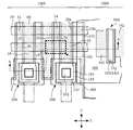
図1および図17は、本実施の形態に係る製造方法によって得られた半導体装置のメモリ領域のレイアウトを示す平面図である。図2は、本実施の形態に係る半導体装置の一部分を示す平面図である。図3は、図2のA−A線に沿った断面図である。
【0029】
図1〜図3および図17に示す半導体装置は、MONOS型不揮発性記憶装置(以下、「メモリセル」という)100が複数の行および列に格子状に配列されてメモリセルアレイを構成しているメモリ領域1000と、メモリの周辺回路などを含むロジック回路領域2000とを含む。
【0030】
(デバイスの構造)
まず、図1および図17を参照しながら、メモリ領域1000のレイアウトについて説明する。
【0031】
図1には、メモリ領域1000の一部である第1のブロックB1と、これに隣り合う第2のブロックB2とが示されている。図17には、第1のブロックB1と、第1のブロックB1のコンタクト構造とが示されている。
【0032】
第1のブロックB1と第2のブロックB2との間の一部領域には、素子分離領域300が形成されている。各ブロックB1,B2においては、X方向(行方向)に延びる複数のワード線50(WL)と、Y方向(列方向)に延びる複数のビット線60(BL)とが設けられている。一本のワード線50は、X方向に配列された複数のワードゲート14に接続されている。ビット線60は不純物層16,18によって構成されている。
【0033】
第1および第2コントロールゲート20,30を構成する導電層40は、各不純物層16,18を囲むように形成されている。すなわち、第1,第2コントロールゲート20,30は、それぞれY方向に延びており、1組の第1,第2コントロールゲート20,30の一方の端部は、X方向に延びる導電層によって互いに接続されている。また、1組の第1,第2コントロールゲート20,30の他方の端部はともに1つの共通コンタクト部200に接続されている。したがって、各第1,第2コントロールゲート20,30は、メモリセルのコントロールゲートの機能と、Y方向に配列された各コントロールゲートを接続する配線としての機能とを有する。
【0034】
単一のメモリセル100は、1つのワードゲート14と、このワードゲート14の両側に形成された第1,第2コントロールゲート20,30と、これらのコントロールゲート20,30の外側であって、半導体基板内に形成された不純物層16,18とを含む。そして、不純物層16,18は、それぞれ隣り合うメモリセル100によって共有される。
【0035】
Y方向に互いに隣り合う不純物層16であって、ブロックB1に形成された不純物層16とブロックB2に形成された不純物層16とは、半導体基板内に形成されたコンタクト用不純物層400によって互いに電気的に接続されている。このコンタクト用不純物層400は、不純物層16に対し、コントロールゲートの共通コンタクト部200とは反対側に形成される。
【0036】
このコンタクト用不純物層400上には、コンタクト350が形成されている。不純物層16によって構成されたビット線60は、このコンタクト350によって、上層の配線層に電気的に接続される。
【0037】
同様に、Y方向に互いに隣り合う2つの不純物層18は、共通コンタクト部200が配置されていない側において、コンタクト用不純物層400によって互いに電気的に接続されている(図17参照)。
【0038】
図1からわかるように、1つのブロックにおいて、複数の共通コンタクト部200の平面レイアウトは、不純物層16と不純物層18とで交互に異なる側に形成され、千鳥配置となる。同様に、図17に示すように、1つのブロックにおいて、複数のコンタクト用不純物層400の平面レイアウトは、不純物層16と不純物層18とで交互に異なる側に形成され、千鳥配置となる。
【0039】
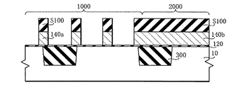
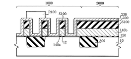
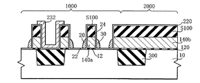
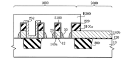
次に、図2および図3を参照しながら、半導体装置の平面構造および断面構造について説明する。メモリ領域1000と隣り合う位置に、例えばメモリの周辺回路を構成するロジック回路領域2000が形成されている。メモリ領域1000とロジック回路領域2000とは、素子分離領域300によって電気的に分離されている。メモリ領域1000には、少なくともメモリセル100が形成されている。ロジック回路領域2000には、少なくともロジック回路を構成する絶縁ゲート電界効果トランジスタ(以下、「MOSトランジスタ」という)500が形成されている。
【0040】
まず、メモリ領域1000について説明する。
【0041】
メモリセル100は、半導体基板10の上方に第1ゲート絶縁層12を介して形成されたワードゲート14と、半導体基板10内に形成された、ソース領域またはドレイン領域を構成する不純物層16,18と、ワードゲート14の両側に沿ってそれぞれ形成された、サイドウォール状の第1および第2のコントロールゲート20,30とを含む。また、不純物層16,18上には、シリサイド層92が形成されている。
【0042】
第1コントロールゲート20は、半導体基板10の上方に第2ゲート絶縁層22を介して形成され、かつ、ワードゲート14の一方の側面に対してサイド絶縁層24を介して形成されている。同様に、第2コントロールゲート30は、半導体基板10の上方に第2ゲート絶縁層22を介して形成され、かつ、ワードゲート14の他方の側面に対してサイド絶縁層24を介して形成されている。
【0043】
第2ゲート絶縁層22およびサイド絶縁層24は、ONO膜である。具体的には、第2ゲート絶縁層22およびサイド絶縁層24は、ボトム酸化シリコン層(第1酸化シリコン層)、窒化シリコン層、トップ酸化シリコン層(第2酸化シリコン層)の積層膜である。
【0044】
第2ゲート絶縁層22の第1酸化シリコン層は、チャネル領域と電荷蓄積領域との間に電位障壁(potential barrier)を形成する。
【0045】
第2ゲート絶縁層22の窒化シリコン層は、キャリア(たとえば電子)をトラップする電荷蓄積領域として機能する。
【0046】
第2ゲート絶縁層22の第2酸化シリコン層は、コントロールゲートと電荷蓄積領域との間に電位障壁(potential barrier)を形成する。
【0047】
サイド絶縁層24は、ワードゲート14と、コントロールゲート20,30とをそれぞれ電気的に分離させる。また、サイド絶縁層24の上端は、ワードゲート14と第1,第2コントロールゲート20,30とのショートを防ぐために、コントロールゲート20,30の上端に比べ、半導体基板10に対して上方に位置している。
【0048】
サイド絶縁層24と第2ゲート絶縁層22とは、同一の成膜工程で形成され、それぞれの層構造は等しくなる。
【0049】
そして、隣り合うメモリセル100において、隣り合う第1コントロールゲート20と第2コントロールゲート30との間には、埋め込み絶縁層70が形成される。この埋め込み絶縁層70は、少なくともコントロールゲート20,30が露出しないようにこれらを覆っている。具体的には、埋込み絶縁層70の上面は、サイド絶縁層24の上端より半導体基板10に対して上方に位置している。埋込み絶縁層70をこのように形成することで、第1,第2コントロールゲート20,30と、ワードゲート14およびワード線50との電気的分離をより確実に行うことができる。
【0050】
共通コンタクト部200には、コントロールゲート20,30に所定の電位を供給するための導電層が形成される。共通コンタクト部200は、第1コンタクト絶縁層212、第2コンタクト絶縁層210、第1コンタクト導電層214、第2コンタクト導電層232、第3コンタクト絶縁層252および第3コンタクト導電層260から構成されている。
【0051】
第1コンタクト絶縁層212は、第1ゲート絶縁層12と同一の工程で形成される。
【0052】
第2コンタクト絶縁層210は、第2ゲート絶縁層22およびサイド絶縁層24と同一の工程で形成される。従って、第2コンタクト絶縁層210は、第1酸化シリコン層,窒化シリコン層および第2酸化シリコン層の積層膜から構成されている。
【0053】
第1コンタクト導電層214は、ワードゲート14と同一の工程で成膜される。この場合、第1コンタクト導電層214は、ワードゲート14と同一の材質から形成される。また、第1コンタクト導電層214は、第2コンタクト絶縁層210の外側に形成されている。さらに、第1コンタクト導電層214は、半導体基板10の上方に第1コンタクト絶縁層212を介して配置されている。
【0054】
第2コンタクト導電層232は、第1コンタクト導電層214の内側に、第2コンタクト絶縁層210を介して配置されている。また、この第2コンタクト導電層232は、半導体基板10の上方に第2コンタクト絶縁層210を介して配置されている。この第2コンタクト導電層232は、第1,第2コントロールゲート20,30の形成と同一の工程によって成膜され、かつ、第1,第2コントロールゲート20,30と連続するように形成されている。したがって、第2コンタクト導電層232と、第1,第2コントロールゲート20,30とは、同一の材質で形成されている。
【0055】
第1サイド絶縁層24,34は、ワードゲート14と、第1,第2コントロールゲート20,30とをそれぞれ電気的に分離させる。また、第1サイド絶縁層24,34の上端は、ワードゲート14と第1,第2コントロールゲート20,30とのショートを防ぐために、第1,第2コントロールゲート20,30の上端に比べ、上方に位置している。
【0056】
本実施の形態では、第1サイド絶縁層24,34と第2ゲート絶縁層22,32とは、同一の成膜工程で形成され、それぞれの層構造は等しくなる。さらに、第1サイド絶縁層24,34は、その上端が第1,第2コントロールゲート20,30より上方に位置するように形成されている。そして、隣り合うメモリセル100において、隣り合う第1コントロールゲート20と第2コントロールゲート30との間には、埋め込み絶縁層70が形成される。本実施の形態においては、第1,第2コントロールゲート20,30は埋め込み絶縁層70によって埋め込まれている。この埋め込み絶縁層70は、少なくとも第1,第2コントロールゲート20,30が露出しないようにこれらを覆っている。具体的には、埋め込み絶縁層70の上面は、第1サイド絶縁層24,34の上端より半導体基板10に対して上方に位置している。埋め込み絶縁層70をこのように形成することで、第1,第2コントロールゲート20,30と、ワードゲート14およびワード線50との電気的分離をより確実に行うことができる。
【0057】
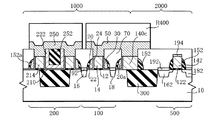
ロジック回路領域2000においては、MOSトランジスタ500が形成されている。MOSトランジスタ500は、半導体基板10の上方に第3ゲート絶縁層122を介して形成されたゲート電極142と、半導体基板10内に形成されたソース領域またはドレイン領域を構成する不純物層162,182と、ゲート電極142の両側面に沿ってそれぞれ形成されたサイドウォール絶縁層152とを含む。さらに、不純物層162,182の上面にはシリサイド層192が形成され、ゲート電極142の上面にはシリサイド層194が形成されている。
【0058】
ロジック回路領域2000においては、MOSトランジスタ500は第2絶縁層270によって覆われている。この第2絶縁層270は、埋込み絶縁層70と同一の工程で形成される。
【0059】
メモリ領域1000とロジック回路領域2000との境界領域には、図2および図3に示すように、ワードゲート14およびゲート電極142と同一の材質からなる境界部140cが形成される。この境界部140cは、ワードゲート14およびゲート電極142と同一の成膜工程で形成される。また、境界部140cの少なくとも一部は、素子分離領域300の上方に形成される。
【0060】
境界部140cの一方の側面(メモリ領域1000側)には、コントロールゲート20,30と同一の材質のサイドウォール状導電層20aが形成されている。このサイドウォール状導電層20aは、Y方向に延びており、共通コンタクト部200を介して隣り合うコントロールゲート30と電気的に接続されている。このサイドウォール状導電層20aは、メモリセルのコントロールゲートとしては利用されない。しかしながら、サイドウォール状導電層20aを隣り合うコントロールゲート30と電気的に接続させることによって、サイドウォール状導電層20aと隣り合うコントロールゲート30の電気特性を、他のコントロールゲートの電気特性と等しくすることができる。
【0061】
また、境界部140cの他の側面(ロジック回路領域2000側)には、MOSトランジスタ500のサイドウォール絶縁層152の形成と同一の工程によって形成されたサイドウォール状絶縁層152が形成されている。
【0062】
メモリセル100およびMOSトランジスタ500などが形成された半導体基板10上には、層間絶縁層72が形成されている。そして、層間絶縁層72には、例えば共通コンタクト部200の第3コンタクト導電層260に到達するコンタクトホール84が形成されている。このコンタクトホール84内に、タングステンプラグまたは銅プラグなどの導電層82が充填され、この導電層82は層間絶縁層72上に形成された配線層80と接続されている。
【0063】
本実施の形態にかかる半導体装置によれば、メモリ領域1000において、サイドウォール状の第1,第2コントロールゲート20,30は、1組ごとに、パッド状の共通コンタクト部200と接続され、この共通コンタクト部200は、第1コンタクト導電層214、第2コンタクト導電層232、およびパッド状の第3コンタクト導電層260を含む。ここで、第3コンタクト導電層260が、第1コンタクト導電層214および第2コンタクト導電層232上に設置されていることにより、これらのコントロールゲートとの電気的接続を確実にとることができる。すなわち、本実施の形態の半導体装置を構成するコントロールゲート20,30は、サイドウォール状の形状を有し、その幅は通常0.1μmより小さい。したがって、第1コンタクト導電層214および第2コンタクト導電層232上に第3コンタクト導電層260を設置させることによって、コントロールゲート20,30と共通コンタクト部200との電気的接続を確保することができる。その結果、コントロールゲートとの電気的コンタクトを上記の共通コンタクト部によって必要最小限の面積で確保することができる。
【0064】
(半導体装置の製造方法)
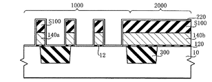
次に、図4〜図15を参照しながら、本実施の形態に係る半導体装置の製造方法について説明する。各断面図は、図2のA−A線に沿った部分に対応する。図4〜図15において、図1〜図3で示す部分と実質的に同一の部分には同一の符号を付し、重複する記載は省略する。
【0065】
(1)図4に示すように、まず、半導体基板10の表面に、トレンチアイソレーション法によって素子分離領域300を形成する。次いで、イオン注入によって、コンタクト用不純物層400(図1参照)を半導体基板10内に形成する。
【0066】
次いで、半導体基板10の表面に、第1ゲート絶縁層となる第1絶縁層120を形成する。次いで、ワードゲート14とゲート電極142とになる第1導電層140を第1絶縁層120上に堆積する。第1導電層140はドープトポリシリコンからなる。次いで、後のCMP工程におけるストッパ層S100を第1導電層140上に形成する。ストッパ層S100は、窒化シリコン層からなる。
【0067】
(2)次いで、ロジック回路領域2000の全てを覆い、さらに、メモリ領域1000の一部にまで張り出したレジスト層(図示しない)を形成する。次いで、このレジスト層をマスクとしてストッパ層S100をパターニングする。その後、パターニングされたストッパ層をマスクとして、第1導電層140をエッチングする。図5に示すように、メモリ領域1000では、第1導電層140がパターニングされゲート層140aとなる。一方、この工程では、ロジック回路領域2000内の第1導電層140はパターニングされない(以後、ロジック回路領域内の第1導電層140を便宜的にゲート層140bと呼ぶ)。
【0068】
パターニング後の様子を平面的に示したのが図6である。このパターニングによって、メモリ領域1000内の第1導電層140およびストッパ層S100の積層体には、開口部160,180が設けられる。開口部160,180は、後のイオン注入によって不純物層16,18が形成される領域にほぼ対応している。そして、後の工程で、開口部160,180の側面に沿ってサイド絶縁層とコントロールゲートとが形成される。
【0069】
(3)図7に示すように、半導体基板10上に、ONO膜220を全面的に形成する。ONO膜220は、第1酸化シリコン層、窒化シリコン層および第2酸化シリコン層を順次堆積させることで形成される。第1酸化シリコン層は、たとえば熱酸化法、CVD法を用いて成膜することができる。窒化シリコン層は、たとえばCVD法によって成膜することができる。第2酸化シリコン層は、CVD法、具体的には高温酸化法(HTO)を用いて成膜することができる。これらの各層を成膜した後、アニール処理を行い、各層を緻密化することが好ましい。
【0070】
ONO膜220は、後のパターニングによって、第2ゲート絶縁層22およびサイド絶縁層24、ならびに第2コンタクト絶縁層210となる(図3参照)。
【0071】
(4)図8に示すように、ドープトポリシリコン層(第2導電層)230を、ONO膜220上に全面的に形成する。ドープトポリシリコン層230は、後にエッチングされて、コントロールゲート20,30を構成する導電層40(図1参照)および共通コンタクト部200の第2コンタクト導電層232(図3参照)となる。
【0072】
次いで、共通コンタクト部200が形成される領域に、レジスト層R100を形成する。
【0073】
(5)図9に示すように、ドープトポリシリコン層230(図8参照)を、レジスト層R100をマスクとして全面的に異方性エッチングすることにより、第1および第2コントロールゲート20,30および第2コンタクト導電層232を形成する。
【0074】
すなわち、このエッチング工程によって、メモリ領域1000の開口部160,180(図6参照)の側面に沿って、サイドウォール状のコントロールゲート20,30が形成される。これと同時に、レジスト層R100(図8参照)でマスクされた部分には、第2コンタクト導電層232が形成される。一方、ロジック回路領域2000内に堆積されたドープトポリシリコン層230は完全に除去される。但し、境界領域においては、ゲート層140bの一方の端部(メモリ領域1000側)の側面に、ドープトポリシリコン層230がサイドウォール状に残存することになる。その後、レジスト層R100は除去される。
【0075】
(6)図10に示すように、メモリ領域1000の全てを覆い、さらにロジック回路領域の一部にまで張り出したレジスト層R200を形成する。次いで、レジスト層R200をマスクとしてロジック回路領域2000におけるONO膜220とストッパ層S100とを除去する。このエッチング工程によって、境界領域を除くロジック回路領域2000内のストッパ層S100は全て除去される。
【0076】
このとき、メモリ領域1000とロジック回路領域2000との境界領域に位置するゲート層140bであって、上記(2)のエッチング工程で使用されるレジスト層と、この(6)のエッチング工程で使用されるレジスト層R200とに共に覆われていた領域は、後の工程で境界部140c(図3参照)となる。また、このパターニングによって形成されたストッパ層S100aは、メモリ領域1000内の他のストッパ層S100より幅が大きい。その後、レジスト層R200は除去される。
【0077】
(7)図11に示すように、ゲート電極142を形成するためのレジスト層R300が形成される。このレジスト層R300は、メモリ領域1000の全てと、ロジック回路領域2000内の所定の部分とを覆うようにパターニングされている。次いで、レジスト層R300をマスクとしてゲート層140b(図10参照)をエッチングすることにより、ロジック回路領域2000内にゲート電極142が形成される。また、このエッチングによって、境界領域にはレジスト層R300とストッパ層S100aとをマスクとして自己整合的に境界部140cがパターニングされる。
【0078】
その後、レジスト層R300は除去される。次いで、N型不純物をドープすることで、ロジック回路領域2000においてソース領域およびドレイン領域のエクステンション層161,181が形成される。
【0079】
(8)図12に示すように、メモリ領域1000およびロジック回路領域2000において、酸化シリコンまたは窒化酸化シリコンなどの絶縁層250を全面的に形成する。
【0080】
(9)図13に示すように、絶縁層250(図12参照)を全面的に異方性エッチングすることにより、ロジック回路領域2000において、ゲート電極142の両側面にサイドウォール絶縁層152が形成される。これと共に、境界部140cのロジック回路領域2000側の側面にサイドウォール絶縁層152が形成さる。また、コントロールゲート20,30上には絶縁層152aが残存させられる。また、第2コンタクト導電層232を覆う第3コンタクト絶縁層252が形成される。さらに、このエッチングによって、後の工程でシリサイド層が形成される領域に堆積された絶縁層は除去され、半導体基板が露出する。
【0081】
このとき、ゲート層140aおよびストッパ層S100の側面に形成された第1サイド絶縁層24,34の上端は、第1,第2コントロールゲート20,30の上端に比べ、上方に位置する。
【0082】
次いで、シリサイド形成用の金属を全面的に堆積させる。シリサイド形成用の金属とは、例えば、チタンやコバルトである。その後、不純物層16,18,162,182と、ゲート電極142との上に形成された金属をシリサイド化反応させることにより、不純物層16,18の上面にシリサイド層92を形成させ、不純物層162,182の上面にシリサイド層192を形成させ、ゲート電極142の上面にシリサイド層194を形成させる。従って、このシリサイド工程によって、ロジック回路領域2000のMOSトランジスタ500は、ゲート電極と、ソース領域またはドレイン領域とが共に自己整合的にシリサイド化される。また、同一のシリサイド工程によって、メモリ領域1000のメモリセル100は、ソース領域またはドレイン領域の表面が自己整合的にシリサイド化される。
【0083】
次いで、メモリ領域1000およびロジック回路領域2000において、酸化シリコンまたは窒化酸化シリコンなどの第2絶縁層270を全面的に形成する。第2絶縁層270は、ストッパ層S100とS100aとを覆うように形成される。
【0084】
(10)図14に示すように、第2絶縁層270を、CMP法を用いて、ストッパ層S100,S100aが露出するまで研磨し、第2絶縁層270を平坦化する。この研磨によって、コントロールゲート20,30をはさんで対向する2つのサイド絶縁層24の間に第2絶縁層270が残存され、埋込み絶縁層70となる。また、図14に示すように、第2コンタクト導電層232から凹部74が構成され、この凹部74に第3コンタクト絶縁層252が形成される。
【0085】
このとき、メモリ領域1000においては、ゲート層140aおよびストッパ層S100の側面に形成されたサイド絶縁層24の上端は、第1,第2コントロールゲート20,30の上端に比べ、半導体基板10に対して上方に位置する。また、ロジック回路領域2000においては、MOSトランジスタ500は第2絶縁層270によって完全に覆われている。
【0086】
従って、この研磨工程が終わった段階で、ワードゲート14となるゲート層140aと境界部140cとの上方にはそれぞれストッパ層S100とS100aとが存在することになる。一方、ゲート電極142の上方にはストッパ層は無く、第2絶縁層270が存在することになる。
【0087】
(11)ストッパ層S100,S100a(図14参照)を熱りん酸で除去する。この結果、少なくともゲート層140aと境界部140cとの上面が露出する。その後、全面的にドープトポリシリコン層(第3導電層、図示せず)を堆積させる。
【0088】
次いで、図15に示すように、前記ドープトポリシリコン層(第3導電層)上に、パターニングされたレジスト層R400を形成する。レジスト層R400をマスクとして、前記ドープトポリシリコン層(第3導電層)をパターニングすることにより、ワード線50と第3コンタクト導電層260とが形成される。
【0089】
引き続き、レジスト層R400をマスクとして、ゲート層140a(図14参照)のエッチングが行われる。このエッチングにより、ワード線50が上方に形成されないゲート層140aが除去される。その結果、アレイ状に配列したワードゲート14を形成することができる。ゲート層140aの除去領域は、後に形成されるP型不純物層(素子分離用不純物層)15の領域と対応する(図2参照)。
【0090】
尚、このエッチング工程では、第1,第2のコントロールゲート20、30をなす導電層40は、埋込み絶縁層70で覆われているために、エッチングされずに残る。また、ロジック回路領域2000のMOSトランジスタ500は、第2絶縁層270によって完全に覆われているため、このエッチングによって影響を受けることは無い。
【0091】
次いで、P型不純物を半導体基板10に全面的にドープする。これにより、Y方向におけるワードゲート14の相互間の領域にP型不純物層(素子分離用不純物層)15(図2参照)が形成される。このP型不純物層15によって、不揮発性半導体記憶装置100相互の素子分離がより確実に行われる。
【0092】
(12)次いで、第1層間絶縁層を形成した後、公知の方法でコンタクトホールを形成し、コンタクトホール内の導電層および第1配線層を形成できる。例えば、図3に示すように、層間絶縁層72にコンタクトホール84を形成した後、共通コンタクト部200と接続された導電層82および配線層80を形成する。この工程では、ロジック回路領域2000においても同様にコンタクト部および配線層を形成することができる。
【0093】
以上の工程により、図1、図2および図3に示す半導体装置を製造することができる。
【0094】
この製造方法による利点は以下の通りである。
【0095】
第1に、特に工程数を増加させることなく、サイドウォール状の第1,第2コントロールゲート20,30とともに共通コンタクト部200を形成できる。そして、共通コンタクト部200は、少なくとも不純物層16,18の幅に近いサイズを有することができ、充分に大きなコンタクト面積を確保できる。したがって、本実施の形態では、充分なコントクト領域をとりにくいサイドウォール状のコントロールゲート20,30であっても、共通コンタクト部200を介して確実な電気的接続をとることができる。
【0096】
第2に、第1コンタクト導電層214および第2コンタクト導電層232上に第3コンタクト導電層260が設置され、この第3コンタクト導電層260上に、導電層82が形成される。したがって、第3コンタクト導電層260が設置されていることにより、この導電層82を形成する際におけるアライメント余裕を確保することができる。
【0097】
第3に、前記(9)の工程によって、メモリセル100のソース領域またはドレイン領域16,18と、MOSトランジスタ500のソース領域またはドレイン領域162,182とを形成するイオン注入工程を同一の工程で行うことができる。
【0098】
第4に、前記(9)の工程によって、メモリセル100のソース領域またはドレイン領域16,18と、MOSトランジスタ500のゲート電極142およびソース領域またはドレイン領域162,182との上にシリサイド層を自己整合的に形成する工程を同一の工程で行うことができる。
【0099】
第5に、メモリセル100のワードゲート14をパターニングする前記(11)の工程において、MOSトランジスタ500は第2絶縁層270で覆われているため、MOSトランジスタ500がエッチングガスに晒され、特性上影響を受けることは無い。
【0100】
第6に、サイドウォール状のコントロールゲートを形成する前記(5)の工程において、メモリセルのコントロールゲートとして機能しないサイドウォール状導電層は境界領域140cの側部に形成される導電層20aのみである。しかしながら、この導電層20aは隣り合うコントロールゲート30と接続されることにより、該コントロールゲート30の電気特性を、他のコントロールゲートの電気特性と等しくすることができる。すわわち、本実施の形態においては、余分なサイドウォール状導電層が形成されることは無い。
【0101】
以上、本発明の一実施の形態について述べたが、本発明はこれに限定されず、本発明の要旨の範囲内で種々の態様をとりうる。たとえば、上記実施の形態では、半導体層としてバルク状の半導体基板を用いたが、SOI基板の半導体層を用いてもよい。
【図面の簡単な説明】
【図1】半導体装置のメモリ領域のレイアウトを模式的に示す平面図である。
【図2】半導体装置の要部を模式的に示す平面図である。
【図3】図2のA−A線に沿った部分を模式的に示す断面図である。
【図4】図1から図3に示す半導体装置の製造方法の一工程を示す断面図である。
【図5】図1から図3に示す半導体装置の製造方法の一工程を示す断面図である。
【図6】図5に示す半導体装置の製造方法の一工程を示す平面図である。
【図7】図1から図3に示す半導体装置の製造方法の一工程を示す断面図である。
【図8】図1から図3に示す半導体装置の製造方法の一工程を示す断面図である。
【図9】図1から図3に示す半導体装置の製造方法の一工程を示す断面図である。
【図10】図1から図3に示す半導体装置の製造方法の一工程を示す断面図である。
【図11】図1から図3に示す半導体装置の製造方法の一工程を示す断面図である。
【図12】図1から図3に示す半導体装置の製造方法の一工程を示す断面図である。
【図13】図1から図3に示す半導体装置の製造方法の一工程を示す断面図である。
【図14】図1から図3に示す半導体装置の製造方法の一工程を示す断面図である。
【図15】図1から図3に示す半導体装置の製造方法の一工程を示す断面図である。
【図16】公知のMONOS型メモリセルを示す断面図である。
【図17】半導体装置のメモリ領域のレイアウトを模式的に示す平面図である。
【符号の説明】
10 半導体基板
12 第1ゲート絶縁層
14 ワードゲート
15 素子分離用不純物層
16,18 不純物層
20 第1コントロールゲート
22 第2ゲート絶縁層
24 サイド絶縁層
30 第2コントロールゲート
40 導電層
50 ワード線
60 ビット線
70 埋込み絶縁層
72 層間絶縁層
74 凹部
80 配線層
82 導電層
84 コンタクトホール
92,192 シリサイド層
100 不揮発性記憶装置(メモリセル)
120 第1ゲート絶縁層(第1絶縁層)
122 第3ゲート絶縁層
140 (第1導電層)
140a,140b ゲート層
142 ゲート電極
162,182 不純物層
160,180 開口部
200 共通コンタクト部
210 第2コンタクト絶縁層
212 第1コンタクト絶縁層
214 第1コンタクト導電層
220 ONO膜
230 ドープドポリシリコン層(第2導電層)
232 第2コンタクト導電層
252 第3コンタクト絶縁層
260 第3コンタクト導電層
270 第2絶縁層
300 素子分離領域
400 コンタクト用不純物層
500 絶縁ゲート電界効果トランジスタ(MOSトランジスタ)
S100 ストッパ層
R100、R200、R300、R400 レジスト層
1000 メモリ領域
2000 ロジック回路領域[0001]
BACKGROUND OF THE INVENTION
The present invention relates to a semiconductor device including a MONOS type nonvolatile memory device and a manufacturing method thereof.
[0002]
[Background Art and Problems to be Solved by the Invention]
As one type of nonvolatile semiconductor memory device, a gate insulating layer between a channel region and a control gate is formed of a laminate of a silicon oxide layer and a silicon nitride layer, and MONOS ( There are types called Metal Oxide Nitride Oxide Semiconductor) or SONOS (Silicon Oxide Nitride Oxide Silicon).
[0003]
A device shown in FIG. 16 is known as a MONOS type nonvolatile semiconductor memory device (reference: Y. Hayashi, et al, 2000 Symposium on VLSI Technology Digest of Technical Papers p. 122-p. 123).
[0004]
In this MONOS
[0005]
As described above, one
[0006]
An object of the present invention is to provide a semiconductor device including a MONOS type nonvolatile memory device and a manufacturing method thereof.
[0007]
[Means for Solving the Problems]
(Semiconductor device)
A semiconductor device according to the present invention includes a memory region that constitutes a memory cell array in which a nonvolatile memory device is arranged in a plurality of rows and columns in a lattice pattern,
The nonvolatile memory device is
A word gate formed above the semiconductor layer via a first gate insulating layer;
An impurity layer forming a source region or a drain region formed in the semiconductor layer;
Sidewall-shaped first and second control gates formed along one side surface and the other side surface of the word gate, respectively.
The first control gate is disposed via a second gate insulating layer with respect to the semiconductor layer and via a side insulating layer with respect to the word gate,
The second control gate is disposed via a second gate insulating layer with respect to the semiconductor layer and via a side insulating layer with respect to the word gate,
The first and second control gates are each continuously arranged in the first direction; and
The second direction crossing the first direction, the first and second control gates adjacent via the impurity layer is connected to the common contact portion,
The common contact portion includes a first contact conductive layer, a second contact conductive layer, and a pad-shaped third contact conductive layer,
The second contact conductive layer is continuous with the first and second control gates and is disposed inside the first contact conductive layer;
The third contact conductive layer is disposed on the first contact conductive layer and the second contact conductive layer.
[0008]
According to the semiconductor device of the present invention, the first and second control gates in the side wall shape are connected to the common contact portion for each set, so that the electrical connection with the control gate having a small width is achieved. It can be taken reliably.
[0009]
The semiconductor device of the present invention can take the following various aspects.
[0010]
(A) The first contact conductive layer is made of the same material as the word gate, the second contact conductive layer is made of the same material as the first and second control gates, and the third contact conductive layer is formed. Can be made of the same material as the word line connected to the word gate.
[0011]
(B) The first contact conductive layer is disposed above the semiconductor layer via a first contact insulating layer, and the second contact conductive layer is disposed above the semiconductor layer. The first contact insulating layer is formed from the same material as the first gate insulating layer, and the second contact insulating layer is formed from the same material as the second gate insulating layer. it can.
[0012]
In this case, the second contact conductive layer can be disposed inside the first contact conductive layer via the second contact insulating layer.
[0013]
In this case, the second contact insulating layer can be formed of the same material as the side insulating layer.
[0014]
(C) The second contact conductive layer may form a recess, and a third contact insulating layer may be embedded in the recess.
[0015]
(D) An upper end of the side insulating layer may be located above the first and second control gates. With this configuration, a buried insulating layer covering the first and second control gates can be reliably formed. That is, the adjacent first and second control gates are covered with the same buried insulating layer, and the buried insulating layers are disposed in contact with the first and second control gates, and the two opposing sides. It is formed between the insulating layers.
[0016]
(E) The common contact portion may be provided adjacent to an end portion of the impurity layer. A plurality of the common contact portions are formed, a plurality of the impurity layers are arranged, and the plurality of common contact portions are arranged with respect to the arranged impurity layers on one side of the impurity layer and the other side. Can be provided alternately at the end on the side.
[0017]
(F) The second gate insulating layer and the side insulating layer can be composed of a laminated film of a first silicon oxide layer, a silicon nitride layer, and a second silicon oxide layer.
[0018]
(Method for manufacturing semiconductor device)
A manufacturing method according to the present invention is a method of manufacturing a semiconductor device including a memory region that constitutes a memory cell array in which a nonvolatile memory device is arranged in a plurality of rows and columns in a grid pattern, and includes the following steps.
[0019]
Forming a first insulating layer for the first gate insulating layer above the semiconductor layer;
Forming a first conductive layer above the first insulating layer;
Forming a stopper layer above the first conductive layer;
Patterning the first conductive layer and the stopper layer to form a gate layer;
Forming a second gate insulating layer at least above the semiconductor layer;
Forming a side insulating layer on both side surfaces of the gate layer;
Forming a second conductive layer in the memory region;
Sidewall-shaped first and second control gates are formed by forming a mask on the second conductive layer corresponding to the formation region of the common contact portion and anisotropically etching the second conductive layer. Process,
After forming the second insulating layer in the memory region, the second insulating layer and the second conductive layer are polished by a chemical mechanical polishing method so that the stopper layer is exposed. Forming a second contact conductive layer in the formation region and then removing the stopper layer;
Forming an impurity layer constituting a source region or a drain region in the semiconductor layer; and forming a third conductive layer in the memory region; and patterning the gate layer and the third conductive layer to form a word gate and Forming a word line connected to the word gate and forming a first contact conductive layer and a third contact conductive layer in a formation region of the common contact portion;
[0020]
According to the method for manufacturing a semiconductor device of the present invention, a common contact portion can be formed together with the sidewall-like first and second control gates without particularly increasing the number of steps, and the semiconductor device can be reliably connected via the common contact portion. Electrical connection can be made.
[0021]
In the manufacturing method according to the present invention, the following embodiments can be further taken.
[0022]
(A) The second gate insulating layer and the side insulating layer are formed in the same film formation step, and may be a stacked film of a first silicon oxide layer, a silicon nitride layer, and a second silicon oxide layer. .
[0023]
(B) The first contact conductive layer can be formed in the same process as the word gate, and the second contact conductive layer can be formed in the same process as the first and second control gates. The third contact conductive layer can be formed in the same process as the word line.
[0024]
(C) in the formation region of the common contact portion, a step of forming a first contact insulating layer above the semiconductor layer; and a second contact insulation above the semiconductor layer and on a side surface of the first contact conductive layer. Forming a layer,
The first contact insulating layer is formed in the same process as the first gate insulating layer, and the second contact insulating layer is formed using the second gate insulating layer and the side insulating layer. It can be performed in the same process as the process of forming.
[0025]
(D) The side insulating layer may be formed such that the upper end thereof is located above the first and second control gates.
[0026]
(E) In the step of polishing the second insulating layer by a chemical mechanical polishing method (hereinafter referred to as “CMP method”), the adjacent first and second control gates are formed to be covered with a buried insulating layer. can do.
[0027]
(F) The common contact portion may be formed adjacent to an end portion of the impurity layer. Also, a plurality of the common contact portions are formed, a plurality of the impurity layers are arranged, and the plurality of common contact portions are arranged with respect to the arranged impurity layers on one side of the impurity layer and the other side. Can be formed alternately at the end of the side.
[0028]
DETAILED DESCRIPTION OF THE INVENTION
1 and 17 are plan views showing the layout of the memory region of the semiconductor device obtained by the manufacturing method according to the present embodiment. FIG. 2 is a plan view showing a part of the semiconductor device according to the present embodiment. 3 is a cross-sectional view taken along line AA in FIG.
[0029]
The semiconductor device shown in FIGS. 1 to 3 and FIG. 17 constitutes a memory cell array in which MONOS nonvolatile memory devices (hereinafter referred to as “memory cells”) 100 are arranged in a plurality of rows and columns in a grid pattern. A
[0030]
(Device structure)
First, the layout of the
[0031]
FIG. 1 shows a first block B1 that is a part of the
[0032]
An
[0033]
The
[0034]
A
[0035]
The impurity layers 16 adjacent to each other in the Y direction, and the
[0036]
A
[0037]
Similarly, two
[0038]
As can be seen from FIG. 1, in one block, the planar layout of the plurality of
[0039]
Next, the planar structure and the cross-sectional structure of the semiconductor device will be described with reference to FIGS. At a position adjacent to the
[0040]
First, the
[0041]
The
[0042]
The
[0043]
The second
[0044]
The first silicon oxide layer of the second
[0045]
The silicon nitride layer of the second
[0046]
The second silicon oxide layer of the second
[0047]
The
[0048]
The
[0049]
In the
[0050]
In the
[0051]
The first
[0052]
The second
[0053]
The first contact
[0054]
The second contact
[0055]
The first
[0056]
In the present embodiment, the first
[0057]
In the
[0058]
In the
[0059]
As shown in FIGS. 2 and 3, a
[0060]
A sidewall-like
[0061]
Further, on the other side surface (on the
[0062]
An interlayer insulating
[0063]
According to the semiconductor device according to the present embodiment, in the
[0064]
(Method for manufacturing semiconductor device)
Next, a method for manufacturing a semiconductor device according to the present embodiment will be described with reference to FIGS. Each cross-sectional view corresponds to a portion along line AA in FIG. 4 to 15, parts that are substantially the same as the parts shown in FIGS. 1 to 3 are given the same reference numerals, and redundant descriptions are omitted.
[0065]
(1) As shown in FIG. 4, first, an
[0066]
Next, a first insulating
[0067]
(2) Next, a resist layer (not shown) that covers the entire
[0068]
FIG. 6 shows a plan view after the patterning. By this patterning,
[0069]
(3) As shown in FIG. 7, an
[0070]
The
[0071]
(4) As shown in FIG. 8, a doped polysilicon layer (second conductive layer) 230 is formed on the entire surface of the
[0072]
Next, a resist layer R100 is formed in a region where the
[0073]
(5) As shown in FIG. 9, the doped polysilicon layer 230 (see FIG. 8) is entirely anisotropically etched using the resist layer R100 as a mask, whereby the first and
[0074]
That is, by this etching process, the sidewall-
[0075]
(6) As shown in FIG. 10, a resist layer R200 that covers the
[0076]
At this time, the
[0077]
(7) As shown in FIG. 11, a resist layer R300 for forming the
[0078]
Thereafter, the resist layer R300 is removed. Next, extension layers 161 and 181 of the source region and the drain region are formed in the
[0079]
(8) As shown in FIG. 12, in the
[0080]
(9) As shown in FIG. 13,
[0081]
At this time, the upper ends of the first
[0082]
Next, a metal for forming a silicide is deposited over the entire surface. The metal for forming the silicide is, for example, titanium or cobalt. Thereafter, the metal formed on the impurity layers 16, 18, 162, 182 and the
[0083]
Next, in the
[0084]
(10) As shown in FIG. 14, the second insulating
[0085]
At this time, in the
[0086]
Therefore, at the stage where this polishing process is completed, the stopper layers S100 and S100a exist above the
[0087]
(11) The stopper layers S100 and S100a (see FIG. 14) are removed with hot phosphoric acid. As a result, at least the upper surfaces of the
[0088]
Next, as shown in FIG. 15, a patterned resist layer R400 is formed on the doped polysilicon layer (third conductive layer). By patterning the doped polysilicon layer (third conductive layer) using the resist layer R400 as a mask, the
[0089]
Subsequently, the
[0090]
In this etching step, the
[0091]
Next, a P-type impurity is entirely doped into the
[0092]
(12) Next, after forming the first interlayer insulating layer, the contact hole can be formed by a known method, and the conductive layer and the first wiring layer in the contact hole can be formed. For example, as shown in FIG. 3, after forming the
[0093]
Through the above steps, the semiconductor device shown in FIGS. 1, 2, and 3 can be manufactured.
[0094]
The advantages of this manufacturing method are as follows.
[0095]
First, the
[0096]
Second, a third contact
[0097]
Third, the ion implantation step for forming the source region or drain
[0098]
Fourth, the silicide layer is formed on the source region or drain
[0099]
Fifth, in the step (11) of patterning the
[0100]
Sixth, in the step (5) of forming the sidewall-like control gate, the sidewall-like conductive layer that does not function as the control gate of the memory cell is only the
[0101]
As mentioned above, although one embodiment of the present invention was described, the present invention is not limited to this, and can take various forms within the scope of the gist of the present invention. For example, in the above embodiment, a bulk semiconductor substrate is used as the semiconductor layer, but a semiconductor layer of an SOI substrate may be used.
[Brief description of the drawings]
FIG. 1 is a plan view schematically showing a layout of a memory region of a semiconductor device.
FIG. 2 is a plan view schematically showing the main part of the semiconductor device.
3 is a cross-sectional view schematically showing a portion along line AA in FIG. 2. FIG.
4 is a cross-sectional view showing a step of the method of manufacturing the semiconductor device shown in FIGS. 1 to 3. FIG.
5 is a cross-sectional view showing a step of the method of manufacturing the semiconductor device shown in FIGS. 1 to 3. FIG.
6 is a plan view showing one step in a method of manufacturing the semiconductor device shown in FIG. 5. FIG.
7 is a cross-sectional view showing a step of the method of manufacturing the semiconductor device shown in FIGS. 1 to 3. FIG.
8 is a cross-sectional view showing a step of the method of manufacturing the semiconductor device shown in FIGS. 1 to 3. FIG.
FIG. 9 is a cross-sectional view showing a step of the method for manufacturing the semiconductor device shown in FIGS. 1 to 3;
10 is a cross-sectional view showing a step of the method of manufacturing the semiconductor device shown in FIGS. 1 to 3. FIG.
11 is a cross-sectional view showing a step of the method of manufacturing the semiconductor device shown in FIGS. 1 to 3. FIG.
12 is a cross-sectional view showing a step of the method of manufacturing the semiconductor device shown in FIGS. 1 to 3. FIG.
13 is a cross-sectional view showing a step of the method of manufacturing the semiconductor device shown in FIGS. 1 to 3. FIG.
14 is a cross-sectional view showing a step of the method of manufacturing the semiconductor device shown in FIGS. 1 to 3. FIG.
15 is a cross-sectional view showing a step of the method of manufacturing the semiconductor device shown in FIGS. 1 to 3. FIG.
FIG. 16 is a cross-sectional view showing a known MONOS type memory cell.
FIG. 17 is a plan view schematically showing a layout of a memory region of a semiconductor device.
[Explanation of symbols]
DESCRIPTION OF
120 First gate insulating layer (first insulating layer)
122 Third gate insulating layer 140 (first conductive layer)
140a,
232 Second contact
S100 Stopper layer R100, R200, R300, R400 Resist
Claims (20)
前記不揮発性記憶装置は、
半導体層の上方に、第1ゲート絶縁層を介して形成されたワードゲートと、
前記半導体層に形成された、ソース領域またはドレイン領域を構成する不純物層と、
前記ワードゲートの一方の側面に沿って列方向に連続して形成された第1コントロールゲートであって、前記半導体層に対して第2ゲート絶縁層を介して、かつ、前記ワードゲートに対してサイド絶縁層を介して配置された、サイドウォール状の前記第1コントロールゲートと、
前記ワードゲートの他方の側面に沿って列方向に連続して形成された第2コントロールゲートであって、前記半導体層に対して第2ゲート絶縁層を介して、かつ、前記ワードゲートに対してサイド絶縁層を介して配置された、サイドウォール状の前記第2コントロールゲートと、を含み、
1つの前記不純物層を共有し行方向に隣り合う2つの不揮発性半導体記憶装置は、該不純物層を挟んで対向する1組の第1コントロールゲートと第2コントロールゲートとが、1つの共通コンタクト部に接続され、
前記共通コンタクト部は、前記第1および第2コントロールゲートと連続した第2コンタクト導電層と、前記第2コンタクト導電層上に形成されたパッド状の第3コンタクト導電層と、を含む、半導体装置。A non-volatile storage device includes a memory region that constitutes a memory cell array arranged in a grid in a plurality of rows and columns,
The nonvolatile memory device is
A word gate formed above the semiconductor layer via a first gate insulating layer;
An impurity layer forming a source region or a drain region formed in the semiconductor layer;
A first control gate continuously formed in a column direction along one side surface of the word gate, the second gate insulating layer with respect to the semiconductor layer and the word gate; The first control gate in the form of a sidewall disposed via a side insulating layer;
A second control gate continuously formed in a column direction along the other side surface of the word gate, the second gate being connected to the semiconductor layer via a second gate insulating layer, and to the word gate The second control gate in the form of a sidewall disposed via a side insulating layer ,
In the two nonvolatile semiconductor memory devices that share one impurity layer and are adjacent to each other in the row direction, a pair of first control gate and second control gate that are opposed to each other with the impurity layer sandwiched therebetween has one common contact portion. Connected to
The common contact portion includes a second contact conductive layer continuous with the first and second control gates, and a pad-like third contact conductive layer formed on the second contact conductive layer. .
前記共通コンタクト部は、さらに、前記第2コンタクト導電層の両側に形成された第1コンタクト導電層を含み、 The common contact part further includes a first contact conductive layer formed on both sides of the second contact conductive layer,
前記第3コンタクト導電層は、前記第1コンタクト導電層上に延設されている、半導体装置。 The semiconductor device, wherein the third contact conductive layer extends on the first contact conductive layer.
前記第1コンタクト導電層は、前記ワードゲートと同一の材質からなり、
前記第2コンタクト導電層は、前記第1および第2コントロールゲートと同一の材質からなり、
前記第3コンタクト導電層は前記ワードゲートに接続されるワード線と同一の材質からなる、半導体装置。In claim 2 ,
The first contact conductive layer is made of the same material as the word gate,
The second contact conductive layer is made of the same material as the first and second control gates,
The third contact conductive layer is a semiconductor device made of the same material as the word line connected to the word gate.
前記第1コンタクト導電層は、前記半導体層の上方に、第1コンタクト絶縁層を介して配置され、
前記第2コンタクト導電層は、前記半導体層の上方に、第2コンタクト絶縁層を介して配置され、
前記第1コンタクト絶縁層は、前記第1ゲート絶縁層と同一の材質からなり、
前記第2コンタクト絶縁層は、前記第2ゲート絶縁層と同一の材質からなる、半導体装置。In claim 2 or 3 ,
The first contact conductive layer is disposed above the semiconductor layer via a first contact insulating layer,
The second contact conductive layer is disposed above the semiconductor layer via a second contact insulating layer,
The first contact insulating layer is made of the same material as the first gate insulating layer,
The semiconductor device, wherein the second contact insulating layer is made of the same material as the second gate insulating layer.
前記第2コンタクト導電層は、前記第1コンタクト導電層の内側に前記第2コンタクト絶縁層を介して配置されている、半導体装置。In claim 4 ,
The semiconductor device, wherein the second contact conductive layer is disposed inside the first contact conductive layer via the second contact insulating layer.
前記第2コンタクト導電層は凹部を構成し、該凹部には第3コンタクト絶縁層が埋め込まれている、半導体装置。In any of claims 1 to 5 ,
The semiconductor device, wherein the second contact conductive layer forms a recess, and a third contact insulating layer is embedded in the recess.
前記第2コンタクト絶縁層は、前記サイド絶縁層と同一の材質からなる、半導体装置。In any of claims 4 to 6 ,
The second contact insulating layer is a semiconductor device made of the same material as the side insulating layer.
前記サイド絶縁層は、その上端が前記第1および第2コントロールゲートより上方に位置する、半導体装置。In any one of Claims 1 thru | or 7 ,
The side insulating layer is a semiconductor device, the upper end of which is located above the first and second control gates.
隣り合う前記第1および第2コントロールゲートは、絶縁層によって埋め込まれている、半導体装置。In any of claims 1 to 8 ,
The adjacent first and second control gates are embedded in an insulating layer.
前記共通コンタクト部は、前記不純物層の端部に隣接して設けられた、半導体装置。In any one of Claim 1 thru | or 9 ,
The common contact portion is a semiconductor device provided adjacent to an end portion of the impurity layer.
前記共通コンタクト部が複数形成され、前記不純物層が複数配列され、
前記複数の共通コンタクト部は、複数配列された前記不純物層に対して、該不純物層の一方の側の端部と他方の側の端部とにおいて交互に設けられた、半導体装置。In claim 10 ,
A plurality of the common contact portions are formed, a plurality of the impurity layers are arranged,
The semiconductor device, wherein the plurality of common contact portions are alternately provided at one end and the other end of the impurity layer with respect to the plurality of impurity layers arranged.
前記第2ゲート絶縁層および前記サイド絶縁層は、第1酸化シリコン層、窒化シリコン層、および第2酸化シリコン層の積層膜からなる、半導体装置。In any one of Claims 1 thru | or 11 ,
The semiconductor device, wherein the second gate insulating layer and the side insulating layer are formed of a stacked film of a first silicon oxide layer, a silicon nitride layer, and a second silicon oxide layer.
半導体層の上方に、第1ゲート絶縁層のための第1絶縁層を形成する工程、
前記第1絶縁層の上方に、第1導電層を形成する工程、
前記第1導電層の上方に、ストッパ層を形成する工程、
前記第1導電層および前記ストッパ層をパターニングして、ゲート層を形成する工程、
少なくとも前記半導体層の上方に、第2ゲート絶縁層を形成する工程、
前記ゲート層の両側面にサイド絶縁層を形成する工程、
前記メモリ領域に第2導電層を形成する工程、
共通コンタクト部の形成領域に対応する前記第2導電層上にマスクを形成して、前記第2導電層を異方性エッチングすることにより、サイドウォール状の第1および第2コントロールゲートを形成する工程、
前記メモリ領域に第2絶縁層を形成した後、前記ストッパ層が露出するように該第2絶縁層および前記第2導電層を化学的機械的研磨法によって研磨することにより、前記共通コンタクト部の形成領域内に第2コンタクト導電層を形成し、その後前記ストッパ層を除去する工程、
ソース領域またはドレイン領域を構成する不純物層を前記半導体層に形成する工程、および
前記メモリ領域に第3導電層を形成した後、前記ゲート層および前記第3導電層をパターニングして、ワードゲートおよび前記ワードゲートに接続されたワード線を形成するとともに、前記共通コンタクト部の形成領域内に第1コンタクト導電層および第3コンタクト導電層を形成する工程。A method of manufacturing a semiconductor device including a memory region that constitutes a memory cell array in which a nonvolatile memory device is arranged in a plurality of rows and columns in a lattice pattern, and includes the following steps.
Forming a first insulating layer for the first gate insulating layer above the semiconductor layer;
Forming a first conductive layer above the first insulating layer;
Forming a stopper layer above the first conductive layer;
Patterning the first conductive layer and the stopper layer to form a gate layer;
Forming a second gate insulating layer at least above the semiconductor layer;
Forming a side insulating layer on both side surfaces of the gate layer;
Forming a second conductive layer in the memory region;
Sidewall-shaped first and second control gates are formed by forming a mask on the second conductive layer corresponding to the formation region of the common contact portion and anisotropically etching the second conductive layer. Process,
After forming the second insulating layer in the memory region, the second insulating layer and the second conductive layer are polished by a chemical mechanical polishing method so that the stopper layer is exposed. Forming a second contact conductive layer in the formation region and then removing the stopper layer;
Forming an impurity layer forming a source region or a drain region in the semiconductor layer; and forming a third conductive layer in the memory region; and patterning the gate layer and the third conductive layer to form a word gate and Forming a word line connected to the word gate and forming a first contact conductive layer and a third contact conductive layer in a formation region of the common contact portion;
前記第2ゲート絶縁層および前記サイド絶縁層は、同一の成膜工程で形成され、かつ、第1酸化シリコン層、窒化シリコン層および第2酸化シリコン層の積層膜からなる、半導体装置の製造方法。In claim 13 ,
The method for manufacturing a semiconductor device, wherein the second gate insulating layer and the side insulating layer are formed in the same film forming step and are formed of a stacked film of a first silicon oxide layer, a silicon nitride layer, and a second silicon oxide layer. .
前記第1コンタクト導電層は前記ワードゲートと同一の工程で成膜され、前記第2コンタクト導電層は前記第1および第2コントロールゲートと同一の工程で成膜され、前記第3コンタクト導電層は前記ワード線と同一の工程で成膜される、半導体装置の製造方法。In claim 13 or 14 ,
The first contact conductive layer is formed in the same process as the word gate, the second contact conductive layer is formed in the same process as the first and second control gates, and the third contact conductive layer is formed A method of manufacturing a semiconductor device, wherein a film is formed in the same step as the word line.
前記共通コンタクト部の形成領域において、さらに、前記半導体層の上方に第1コンタクト絶縁層を形成する工程と、前記半導体層の上方および前記第1コンタクト導電層の側面に第2コンタクト絶縁層を形成する工程とを含み、
前記第1コンタクト絶縁層の形成は、前記第1ゲート絶縁層を形成する工程と同一工程にて行なわれ、
前記第2コンタクト絶縁層の形成は、前記第2ゲート絶縁層および前記サイド絶縁層を形成する工程と同一工程にて行なわれる、半導体装置の製造方法。In any of claims 13 to 15 ,
Forming a first contact insulating layer above the semiconductor layer and forming a second contact insulating layer above the semiconductor layer and on a side surface of the first contact conductive layer in the common contact portion formation region; Including the steps of:
The first contact insulating layer is formed in the same step as the step of forming the first gate insulating layer,
The method of manufacturing a semiconductor device, wherein the formation of the second contact insulating layer is performed in the same step as the step of forming the second gate insulating layer and the side insulating layer.
前記サイド絶縁層を、その上端が前記第1および第2コントロールゲートより上方に位置するように形成する、半導体装置の製造方法。In any of claims 13 to 16 ,
A method of manufacturing a semiconductor device, wherein the side insulating layer is formed such that an upper end thereof is located above the first and second control gates.
前記第2絶縁層を化学的機械的研磨法によって研磨する工程において、前記不純物層を介して隣り合う前記第1および第2コントロールゲートは埋込み絶縁層によって覆われるように形成される、半導体装置の製造方法。In any of claims 13 to 17 ,
In the step of polishing the second insulating layer by a chemical mechanical polishing method, the first and second control gates adjacent to each other through the impurity layer are formed to be covered with a buried insulating layer. Production method.
前記共通コンタクト部は、前記不純物層の端部に隣接して形成される、半導体装置の製造方法。In any of claims 13 to 18 ,
The semiconductor device manufacturing method, wherein the common contact portion is formed adjacent to an end portion of the impurity layer.
前記共通コンタクト部を複数形成し、前記不純物層を複数配列させ、
前記複数の共通コンタクト部は、複数配列された前記不純物層に対して、該不純物層の一方の側の端部と他方の側の端部とにおいて交互に形成される、半導体装置の製造方法。In any of claims 13 to 19 ,
Forming a plurality of common contact portions, arranging a plurality of impurity layers;
The method for manufacturing a semiconductor device, wherein the plurality of common contact portions are alternately formed at one end and the other end of the impurity layer with respect to the plurality of impurity layers arranged.
Priority Applications (4)
| Application Number | Priority Date | Filing Date | Title |
|---|---|---|---|
| JP2001292126A JP3674564B2 (en) | 2001-09-25 | 2001-09-25 | Semiconductor device and manufacturing method thereof |
| US10/244,627 US6891271B2 (en) | 2001-09-25 | 2002-09-17 | Non-volatile memory device |
| CNB021425930A CN1290195C (en) | 2001-09-25 | 2002-09-24 | Semiconductor device and its mfg. method |
| US10/939,330 US7005328B2 (en) | 2001-09-25 | 2004-09-14 | Non-volatile memory device |
Applications Claiming Priority (1)
| Application Number | Priority Date | Filing Date | Title |
|---|---|---|---|
| JP2001292126A JP3674564B2 (en) | 2001-09-25 | 2001-09-25 | Semiconductor device and manufacturing method thereof |
Publications (3)
| Publication Number | Publication Date |
|---|---|
| JP2003100915A JP2003100915A (en) | 2003-04-04 |
| JP3674564B2 true JP3674564B2 (en) | 2005-07-20 |
| JP2003100915A5 JP2003100915A5 (en) | 2005-09-08 |
Family
ID=19114145
Family Applications (1)
| Application Number | Title | Priority Date | Filing Date |
|---|---|---|---|
| JP2001292126A Expired - Fee Related JP3674564B2 (en) | 2001-09-25 | 2001-09-25 | Semiconductor device and manufacturing method thereof |
Country Status (3)
| Country | Link |
|---|---|
| US (2) | US6891271B2 (en) |
| JP (1) | JP3674564B2 (en) |
| CN (1) | CN1290195C (en) |
Families Citing this family (35)
| Publication number | Priority date | Publication date | Assignee | Title |
|---|---|---|---|---|
| JP3671889B2 (en) * | 2001-09-25 | 2005-07-13 | セイコーエプソン株式会社 | Semiconductor device and manufacturing method thereof |
| JP2003243542A (en) * | 2002-02-15 | 2003-08-29 | Seiko Epson Corp | Manufacturing method for non-volatile storage |
| JP2003243617A (en) | 2002-02-20 | 2003-08-29 | Seiko Epson Corp | Manufacturing method of semiconductor device |
| JP3726760B2 (en) | 2002-02-20 | 2005-12-14 | セイコーエプソン株式会社 | Manufacturing method of semiconductor device |
| JP2003243616A (en) * | 2002-02-20 | 2003-08-29 | Seiko Epson Corp | Manufacturing method of semiconductor device |
| JP2003243618A (en) | 2002-02-20 | 2003-08-29 | Seiko Epson Corp | Manufacturing method of semiconductor device |
| JP2003249575A (en) * | 2002-02-22 | 2003-09-05 | Seiko Epson Corp | Method of manufacturing non-volatile memory device |
| JP2003258129A (en) * | 2002-03-01 | 2003-09-12 | Seiko Epson Corp | Manufacturing method of non-volatile memory device |
| JP2003258133A (en) | 2002-03-05 | 2003-09-12 | Seiko Epson Corp | Manufacturing method of non-volatile memory device, and manufacturing method of semiconductor device |
| JP2003258132A (en) | 2002-03-05 | 2003-09-12 | Seiko Epson Corp | Manufacturing method of non-volatile memory device |
| JP3640186B2 (en) * | 2002-03-06 | 2005-04-20 | セイコーエプソン株式会社 | Manufacturing method of semiconductor device |
| JP2003282744A (en) * | 2002-03-22 | 2003-10-03 | Seiko Epson Corp | Nonvolatile memory device |
| JP3975349B2 (en) * | 2002-09-02 | 2007-09-12 | セイコーエプソン株式会社 | Semiconductor device and manufacturing method thereof |
| JP3975350B2 (en) * | 2002-09-11 | 2007-09-12 | セイコーエプソン株式会社 | Manufacturing method of semiconductor device |
| JP3972196B2 (en) * | 2002-09-18 | 2007-09-05 | セイコーエプソン株式会社 | Manufacturing method of semiconductor device |
| JP3743514B2 (en) * | 2002-10-24 | 2006-02-08 | セイコーエプソン株式会社 | Semiconductor device and manufacturing method thereof |
| JP3664159B2 (en) * | 2002-10-29 | 2005-06-22 | セイコーエプソン株式会社 | Semiconductor device and manufacturing method thereof |
| JP3664161B2 (en) * | 2002-10-30 | 2005-06-22 | セイコーエプソン株式会社 | Semiconductor device and manufacturing method thereof |
| JP3664160B2 (en) | 2002-10-30 | 2005-06-22 | セイコーエプソン株式会社 | Semiconductor device and manufacturing method thereof |
| JP4841123B2 (en) * | 2004-07-28 | 2011-12-21 | パナソニック株式会社 | Semiconductor memory device and manufacturing method thereof |
| JP4758625B2 (en) * | 2004-08-09 | 2011-08-31 | ルネサスエレクトロニクス株式会社 | Semiconductor device |
| JP4462424B2 (en) * | 2005-02-03 | 2010-05-12 | セイコーエプソン株式会社 | Semiconductor device |
| US7491622B2 (en) * | 2006-04-24 | 2009-02-17 | Freescale Semiconductor, Inc. | Process of forming an electronic device including a layer formed using an inductively coupled plasma |
| US7670895B2 (en) | 2006-04-24 | 2010-03-02 | Freescale Semiconductor, Inc | Process of forming an electronic device including a semiconductor layer and another layer adjacent to an opening within the semiconductor layer |
| US20070249127A1 (en) * | 2006-04-24 | 2007-10-25 | Freescale Semiconductor, Inc. | Electronic device including a semiconductor layer and a sidewall spacer and a process of forming the same |
| US7528078B2 (en) * | 2006-05-12 | 2009-05-05 | Freescale Semiconductor, Inc. | Process of forming electronic device including a densified nitride layer adjacent to an opening within a semiconductor layer |
| JP4758951B2 (en) * | 2007-06-12 | 2011-08-31 | ルネサスエレクトロニクス株式会社 | Semiconductor device |
| JP2010267732A (en) * | 2009-05-13 | 2010-11-25 | Panasonic Corp | Method for manufacturing nonvolatile semiconductor memory device |
| JP2011171755A (en) * | 2011-04-15 | 2011-09-01 | Renesas Electronics Corp | Semiconductor device |
| US10332882B2 (en) * | 2013-12-30 | 2019-06-25 | Taiwan Semiconductor Manufacturing Co., Ltd. | Semiconductor device having protective structure over shallow trench isolation region and fabricating method thereof |
| US9425206B2 (en) * | 2014-12-23 | 2016-08-23 | Taiwan Semiconductor Manufacturing Co., Ltd. | Boundary scheme for embedded poly-SiON CMOS or NVM in HKMG CMOS technology |
| US9917165B2 (en) * | 2015-05-15 | 2018-03-13 | Taiwan Semiconductor Manufacturing Co., Ltd. | Memory cell structure for improving erase speed |
| DE102016114799B4 (en) * | 2015-12-30 | 2021-01-28 | Taiwan Semiconductor Manufacturing Company, Ltd. | In-depth STI as a gate dielectric of a high voltage device and manufacturing process |
| US10756113B2 (en) * | 2017-11-23 | 2020-08-25 | Yangtze Memory Technologies Co., Ltd. | Protective structure and fabrication methods for the peripheral circuits of a three-dimensional memory |
| US10867851B2 (en) * | 2018-02-26 | 2020-12-15 | Taiwan Semiconductor Manufacturing Company, Ltd. | Contact structure and semiconductor device and method of forming the same |
Family Cites Families (32)
| Publication number | Priority date | Publication date | Assignee | Title |
|---|---|---|---|---|
| JPH07161851A (en) | 1993-12-10 | 1995-06-23 | Sony Corp | Semiconductor nonvolatile memory and its manufacture |
| US5408115A (en) | 1994-04-04 | 1995-04-18 | Motorola Inc. | Self-aligned, split-gate EEPROM device |
| US5422504A (en) | 1994-05-02 | 1995-06-06 | Motorola Inc. | EEPROM memory device having a sidewall spacer floating gate electrode and process |
| US5663923A (en) | 1995-04-28 | 1997-09-02 | Intel Corporation | Nonvolatile memory blocking architecture |
| US5969383A (en) | 1997-06-16 | 1999-10-19 | Motorola, Inc. | Split-gate memory device and method for accessing the same |
| JP2978477B1 (en) | 1998-06-12 | 1999-11-15 | 株式会社日立製作所 | Semiconductor integrated circuit device and method of manufacturing the same |
| JP3973819B2 (en) | 1999-03-08 | 2007-09-12 | 株式会社東芝 | Semiconductor memory device and manufacturing method thereof |
| US6255166B1 (en) | 1999-08-05 | 2001-07-03 | Aalo Lsi Design & Device Technology, Inc. | Nonvolatile memory cell, method of programming the same and nonvolatile memory array |
| US6177318B1 (en) | 1999-10-18 | 2001-01-23 | Halo Lsi Design & Device Technology, Inc. | Integration method for sidewall split gate monos transistor |
| US6248633B1 (en) * | 1999-10-25 | 2001-06-19 | Halo Lsi Design & Device Technology, Inc. | Process for making and programming and operating a dual-bit multi-level ballistic MONOS memory |
| DE10010089A1 (en) | 2000-03-02 | 2001-09-06 | Epcos Ag | Interdigital transducer for surface acoustic wave filter, has same phase excitation and reflection in several base cells |
| JP4325972B2 (en) | 2001-01-30 | 2009-09-02 | セイコーエプソン株式会社 | Manufacturing method of semiconductor integrated circuit device including nonvolatile semiconductor memory device |
| JP3496932B2 (en) | 2001-01-30 | 2004-02-16 | セイコーエプソン株式会社 | Semiconductor integrated circuit device including nonvolatile semiconductor memory device |
| JP3452056B2 (en) | 2001-09-14 | 2003-09-29 | セイコーエプソン株式会社 | Method for manufacturing semiconductor device |
| US6518124B1 (en) | 2001-09-18 | 2003-02-11 | Seiko Epson Corporation | Method of fabricating semiconductor device |
| US6413821B1 (en) | 2001-09-18 | 2002-07-02 | Seiko Epson Corporation | Method of fabricating semiconductor device including nonvolatile memory and peripheral circuit |
| JP3671889B2 (en) | 2001-09-25 | 2005-07-13 | セイコーエプソン株式会社 | Semiconductor device and manufacturing method thereof |
| JP3956709B2 (en) | 2002-01-23 | 2007-08-08 | セイコーエプソン株式会社 | Manufacturing method of semiconductor device |
| JP3531641B2 (en) | 2002-01-24 | 2004-05-31 | セイコーエプソン株式会社 | Method for manufacturing semiconductor device |
| JP2003218244A (en) | 2002-01-24 | 2003-07-31 | Seiko Epson Corp | Method of manufacturing semiconductor device |
| JP2003243617A (en) | 2002-02-20 | 2003-08-29 | Seiko Epson Corp | Manufacturing method of semiconductor device |
| JP3726760B2 (en) | 2002-02-20 | 2005-12-14 | セイコーエプソン株式会社 | Manufacturing method of semiconductor device |
| JP2003243618A (en) | 2002-02-20 | 2003-08-29 | Seiko Epson Corp | Manufacturing method of semiconductor device |
| JP2003243616A (en) | 2002-02-20 | 2003-08-29 | Seiko Epson Corp | Manufacturing method of semiconductor device |
| JP3622741B2 (en) | 2002-07-12 | 2005-02-23 | セイコーエプソン株式会社 | Manufacturing method of semiconductor device |
| JP3975349B2 (en) | 2002-09-02 | 2007-09-12 | セイコーエプソン株式会社 | Semiconductor device and manufacturing method thereof |
| JP3975350B2 (en) | 2002-09-11 | 2007-09-12 | セイコーエプソン株式会社 | Manufacturing method of semiconductor device |
| JP3972196B2 (en) | 2002-09-18 | 2007-09-05 | セイコーエプソン株式会社 | Manufacturing method of semiconductor device |
| JP3743514B2 (en) | 2002-10-24 | 2006-02-08 | セイコーエプソン株式会社 | Semiconductor device and manufacturing method thereof |
| JP3664159B2 (en) | 2002-10-29 | 2005-06-22 | セイコーエプソン株式会社 | Semiconductor device and manufacturing method thereof |
| JP3664160B2 (en) | 2002-10-30 | 2005-06-22 | セイコーエプソン株式会社 | Semiconductor device and manufacturing method thereof |
| JP3664161B2 (en) | 2002-10-30 | 2005-06-22 | セイコーエプソン株式会社 | Semiconductor device and manufacturing method thereof |
-
2001
- 2001-09-25 JP JP2001292126A patent/JP3674564B2/en not_active Expired - Fee Related
-
2002
- 2002-09-17 US US10/244,627 patent/US6891271B2/en not_active Expired - Fee Related
- 2002-09-24 CN CNB021425930A patent/CN1290195C/en not_active Expired - Fee Related
-
2004
- 2004-09-14 US US10/939,330 patent/US7005328B2/en not_active Expired - Fee Related
Also Published As
| Publication number | Publication date |
|---|---|
| US7005328B2 (en) | 2006-02-28 |
| US20030057505A1 (en) | 2003-03-27 |
| JP2003100915A (en) | 2003-04-04 |
| US20050032312A1 (en) | 2005-02-10 |
| US6891271B2 (en) | 2005-05-10 |
| CN1494154A (en) | 2004-05-05 |
| CN1290195C (en) | 2006-12-13 |
Similar Documents
| Publication | Publication Date | Title |
|---|---|---|
| JP3674564B2 (en) | Semiconductor device and manufacturing method thereof | |
| US6413821B1 (en) | Method of fabricating semiconductor device including nonvolatile memory and peripheral circuit | |
| JP3452056B2 (en) | Method for manufacturing semiconductor device | |
| JP3671889B2 (en) | Semiconductor device and manufacturing method thereof | |
| JP3726760B2 (en) | Manufacturing method of semiconductor device | |
| JP4325972B2 (en) | Manufacturing method of semiconductor integrated circuit device including nonvolatile semiconductor memory device | |
| JP5520185B2 (en) | Semiconductor device and manufacturing method thereof | |
| JP3671890B2 (en) | Semiconductor device and manufacturing method thereof | |
| US6518124B1 (en) | Method of fabricating semiconductor device | |
| JP3956709B2 (en) | Manufacturing method of semiconductor device | |
| US6706579B2 (en) | Method of manufacturing semiconductor device | |
| JP3531641B2 (en) | Method for manufacturing semiconductor device | |
| JP3640186B2 (en) | Manufacturing method of semiconductor device | |
| JP2003243617A (en) | Manufacturing method of semiconductor device | |
| JP3812645B2 (en) | Semiconductor device | |
| JP2003218244A (en) | Method of manufacturing semiconductor device | |
| JP3849759B2 (en) | Semiconductor device | |
| JP2003243616A (en) | Manufacturing method of semiconductor device | |
| JP3622741B2 (en) | Manufacturing method of semiconductor device | |
| JP4300394B2 (en) | Manufacturing method of semiconductor device | |
| JP3675381B2 (en) | Manufacturing method of semiconductor device | |
| JP2003258133A (en) | Manufacturing method of non-volatile memory device, and manufacturing method of semiconductor device | |
| JP3653540B2 (en) | Manufacturing method of semiconductor device | |
| JP4314452B2 (en) | Nonvolatile memory device manufacturing method and semiconductor device manufacturing method |
Legal Events
| Date | Code | Title | Description |
|---|---|---|---|
| A521 | Request for written amendment filed |
Free format text: JAPANESE INTERMEDIATE CODE: A523 Effective date: 20050310 |
|
| TRDD | Decision of grant or rejection written | ||
| A01 | Written decision to grant a patent or to grant a registration (utility model) |
Free format text: JAPANESE INTERMEDIATE CODE: A01 Effective date: 20050405 |
|
| A61 | First payment of annual fees (during grant procedure) |
Free format text: JAPANESE INTERMEDIATE CODE: A61 Effective date: 20050418 |
|
| R150 | Certificate of patent or registration of utility model |
Free format text: JAPANESE INTERMEDIATE CODE: R150 |
|
| FPAY | Renewal fee payment (event date is renewal date of database) |
Free format text: PAYMENT UNTIL: 20090513 Year of fee payment: 4 |
|
| FPAY | Renewal fee payment (event date is renewal date of database) |
Free format text: PAYMENT UNTIL: 20100513 Year of fee payment: 5 |
|
| FPAY | Renewal fee payment (event date is renewal date of database) |
Free format text: PAYMENT UNTIL: 20110513 Year of fee payment: 6 |
|
| FPAY | Renewal fee payment (event date is renewal date of database) |
Free format text: PAYMENT UNTIL: 20120513 Year of fee payment: 7 |
|
| FPAY | Renewal fee payment (event date is renewal date of database) |
Free format text: PAYMENT UNTIL: 20130513 Year of fee payment: 8 |
|
| LAPS | Cancellation because of no payment of annual fees |