JP3670577B2 - Liquid crystal display device and manufacturing method thereof - Google Patents
Liquid crystal display device and manufacturing method thereof Download PDFInfo
- Publication number
- JP3670577B2 JP3670577B2 JP2000380526A JP2000380526A JP3670577B2 JP 3670577 B2 JP3670577 B2 JP 3670577B2 JP 2000380526 A JP2000380526 A JP 2000380526A JP 2000380526 A JP2000380526 A JP 2000380526A JP 3670577 B2 JP3670577 B2 JP 3670577B2
- Authority
- JP
- Japan
- Prior art keywords
- layer
- liquid crystal
- display device
- crystal display
- electrode
- Prior art date
- Legal status (The legal status is an assumption and is not a legal conclusion. Google has not performed a legal analysis and makes no representation as to the accuracy of the status listed.)
- Expired - Fee Related
Links
Images


Classifications
-
- G—PHYSICS
- G02—OPTICS
- G02F—OPTICAL DEVICES OR ARRANGEMENTS FOR THE CONTROL OF LIGHT BY MODIFICATION OF THE OPTICAL PROPERTIES OF THE MEDIA OF THE ELEMENTS INVOLVED THEREIN; NON-LINEAR OPTICS; FREQUENCY-CHANGING OF LIGHT; OPTICAL LOGIC ELEMENTS; OPTICAL ANALOGUE/DIGITAL CONVERTERS
- G02F1/00—Devices or arrangements for the control of the intensity, colour, phase, polarisation or direction of light arriving from an independent light source, e.g. switching, gating or modulating; Non-linear optics
- G02F1/01—Devices or arrangements for the control of the intensity, colour, phase, polarisation or direction of light arriving from an independent light source, e.g. switching, gating or modulating; Non-linear optics for the control of the intensity, phase, polarisation or colour
- G02F1/13—Devices or arrangements for the control of the intensity, colour, phase, polarisation or direction of light arriving from an independent light source, e.g. switching, gating or modulating; Non-linear optics for the control of the intensity, phase, polarisation or colour based on liquid crystals, e.g. single liquid crystal display cells
- G02F1/133—Constructional arrangements; Operation of liquid crystal cells; Circuit arrangements
- G02F1/1333—Constructional arrangements; Manufacturing methods
- G02F1/1343—Electrodes
-
- G—PHYSICS
- G02—OPTICS
- G02F—OPTICAL DEVICES OR ARRANGEMENTS FOR THE CONTROL OF LIGHT BY MODIFICATION OF THE OPTICAL PROPERTIES OF THE MEDIA OF THE ELEMENTS INVOLVED THEREIN; NON-LINEAR OPTICS; FREQUENCY-CHANGING OF LIGHT; OPTICAL LOGIC ELEMENTS; OPTICAL ANALOGUE/DIGITAL CONVERTERS
- G02F1/00—Devices or arrangements for the control of the intensity, colour, phase, polarisation or direction of light arriving from an independent light source, e.g. switching, gating or modulating; Non-linear optics
- G02F1/01—Devices or arrangements for the control of the intensity, colour, phase, polarisation or direction of light arriving from an independent light source, e.g. switching, gating or modulating; Non-linear optics for the control of the intensity, phase, polarisation or colour
- G02F1/13—Devices or arrangements for the control of the intensity, colour, phase, polarisation or direction of light arriving from an independent light source, e.g. switching, gating or modulating; Non-linear optics for the control of the intensity, phase, polarisation or colour based on liquid crystals, e.g. single liquid crystal display cells
- G02F1/133—Constructional arrangements; Operation of liquid crystal cells; Circuit arrangements
- G02F1/1333—Constructional arrangements; Manufacturing methods
- G02F1/1335—Structural association of cells with optical devices, e.g. polarisers or reflectors
- G02F1/133553—Reflecting elements
-
- G—PHYSICS
- G02—OPTICS
- G02F—OPTICAL DEVICES OR ARRANGEMENTS FOR THE CONTROL OF LIGHT BY MODIFICATION OF THE OPTICAL PROPERTIES OF THE MEDIA OF THE ELEMENTS INVOLVED THEREIN; NON-LINEAR OPTICS; FREQUENCY-CHANGING OF LIGHT; OPTICAL LOGIC ELEMENTS; OPTICAL ANALOGUE/DIGITAL CONVERTERS
- G02F1/00—Devices or arrangements for the control of the intensity, colour, phase, polarisation or direction of light arriving from an independent light source, e.g. switching, gating or modulating; Non-linear optics
- G02F1/01—Devices or arrangements for the control of the intensity, colour, phase, polarisation or direction of light arriving from an independent light source, e.g. switching, gating or modulating; Non-linear optics for the control of the intensity, phase, polarisation or colour
- G02F1/13—Devices or arrangements for the control of the intensity, colour, phase, polarisation or direction of light arriving from an independent light source, e.g. switching, gating or modulating; Non-linear optics for the control of the intensity, phase, polarisation or colour based on liquid crystals, e.g. single liquid crystal display cells
- G02F1/133—Constructional arrangements; Operation of liquid crystal cells; Circuit arrangements
- G02F1/1333—Constructional arrangements; Manufacturing methods
- G02F1/1345—Conductors connecting electrodes to cell terminals
- G02F1/13452—Conductors connecting driver circuitry and terminals of panels
-
- G—PHYSICS
- G02—OPTICS
- G02F—OPTICAL DEVICES OR ARRANGEMENTS FOR THE CONTROL OF LIGHT BY MODIFICATION OF THE OPTICAL PROPERTIES OF THE MEDIA OF THE ELEMENTS INVOLVED THEREIN; NON-LINEAR OPTICS; FREQUENCY-CHANGING OF LIGHT; OPTICAL LOGIC ELEMENTS; OPTICAL ANALOGUE/DIGITAL CONVERTERS
- G02F2201/00—Constructional arrangements not provided for in groups G02F1/00 - G02F7/00
- G02F2201/12—Constructional arrangements not provided for in groups G02F1/00 - G02F7/00 electrode
- G02F2201/123—Constructional arrangements not provided for in groups G02F1/00 - G02F7/00 electrode pixel
Description
【0001】
【発明の属する技術分野】
本発明は、液晶表示装置、配線基板およびこれらの製造方法に関し、特に、周囲光を利用して反射モードで表示を行うことが可能な液晶表示装置およびその製造方法に関する。
【0002】
【従来の技術】
近年、ワードプロセッサ、ラップトップ型パーソナルコンピュータ、ポケットテレビなどへの液晶表示装置の応用が急速に進展している。特に、液晶表示装置の中でも周囲光を反射させて表示を行うことが可能な反射型液晶表示装置は、バックライトが不要であるので、消費電力が低く、薄型であり、軽量化が可能であるため注目されている。また、最近、反射モードおよび透過モードの両方で表示が可能な両用型液晶表示装置も開発されている。
【0003】
周囲光を反射するために、従来は、液晶表示装置の基板(TFT基板または観察者とは反対側に設けられた基板)の外側に反射板または反射層を設置していた。液晶表示装置の大容量化に伴い絵素サイズが小さくなると、このような構造では、カラーフィルタ(画素部)と反射板(反射層)との距離の差に起因する視差によって表示品位が低下するという問題が生じる。
【0004】
この問題を解決するために、反射層を基板の液晶層側に設け、さらに、この反射層自体を、液晶層に電圧を印加するための電極(たとえば、TFT型液晶表示装置における絵素電極)として利用する構成が広く用いられるようになった。この反射層を形成する材料としては、高い反射率、優れたパターニング性、低い電気抵抗を有することから、Al(およびAl合金)が使用されることが多い。
【0005】
一方、ITO層とAl層とが互いに接触した状態でこれらがアルカリ溶液に曝されると、ITOとAlとの間で電食が発生し、ITO層およびAl層の一部が欠落するという問題が発生することが知られている。なお、以下の記載において、特にことわらない限り、ITO層というときは、パターニング前のITO層のみならず、パターニング後のITO層をも意味する。
【0006】
特開平3−246524号公報は、従来ITO層を用いて形成されていた表示電極または配線の電気抵抗を低下させるために採用されている、Al層/ITO層の2層構造において、ITO層とAl層との間に、MoまたはMo合金(Mo−Ti等)からなる保護層を設けることによって、Al層にピンホールが存在しても、Al層上に形成されたレジスト層をアルカリ現像する工程においてITO層が欠落する問題を解決できることを開示している。
【0007】
【発明が解決しようとする課題】
しかしながら、上記特開平3−246524号公報に記載されている方法を採用して、ITO層とAl層との間にMo層(Mo合金層を含む)を形成することによってITOとAlとの電食を防止しても、Al層にピンホールが存在すると、アルカリ系の現像液や剥離液、あるいはエッチャントにAl層が曝されると、ピンホールを中心にAl層が腐食され、部分的に欠落することを本願発明者は見出した。なお、上記公報に開示されている方法は、ITOとAlとの電食を防止するために、Al層とITO層とが直接接触することを防止する中間層として、Al層のエッチング工程と同一の工程でエッチングされ得るMo層(またはMo合金層)を形成するものであり、Al層に形成されるピンホールそのものの形成を抑制・防止するものではない。
【0008】
反射電極の一部としてAl層を用いる構成において、Al層の一部が欠落すると、反射電極(反射層)の面積が減少することになり、周囲光を反射する機能が低下するという問題が発生する。具体的には、Al層を反射層として用いる液晶表示装置の製造方法において、例えば、Al層をパターニングするためのマスクとして用いるレジストパターンを形成するために、レジスト層をアルカリ系現像液を用いて現像する工程や、Al層をパターニングした後にレジストパターンをアルカリ系剥離液を用いて剥離する工程において、ピンホールを有するAl層がアルカリ系の現像液や剥離液に曝されると、そのピンホールを中心にAl層の一部(典型的には、直径が2〜5μmの円)が欠落する。なお、Al層の部分的な欠落の発生(ピンホールの成長)は、現像工程よりも剥離工程において顕著である。これは、剥離液がレジスト層を分解する能力は現像液よりも高いこと、および剥離液に曝されるAl層の表面積が現像液に曝されるAl層の表面積よりも広いことに起因する。
【0009】
また、Al層をパターニングする工程においては、Al層の一部が欠落する現象によって、パターニングされたAl層の周辺がガタガタ(切手の縁のように)になる。Al層のパターニングは種々の材料(アルカリ性または酸性溶液など)および方法を用いて実行することができる。なお、エッチング法を採用した場合、Al層の部分的な欠落は、Al層/Mo層の積層構造を同一エッチャントを用いてエッチングできるという利点を有するウエットエッチング法においてドライエッチング法よりも顕著である。
【0010】
Al層が端子電極の最上層のITO層上に一時的に堆積された後、前記Al層を除去する場合、ITOとAlとの電食によってITO層が部分的に欠落して、不具合が生じることがある。例えば、端子領域に形成される走査線端子電極などの端子電極の最上層がITO層であって、反射層を形成するためのAl層がこのITO層上に一時的に堆積された場合、Al層をエッチャントにて除去したとき、ITO層が電食によって欠落して、端子電極の信頼性が損なわれるおそれがある。
【0011】
Al層の部分的な欠落は、Al層を反射層として用いた液晶表示装置のみならず、配線または電極などにAl層/ITO層の2層構造を用いた液晶表示装置または他の装置、例えば有機ELを用いた表示装置および太陽電池などについても不具合を生じさせる。例えば、TFTアクティブマトリクス型液晶表示装置において、信号線をAl層/ITO層の2層構造とした場合、Al層の欠落の程度が大きいと、Al層の幅が狭くなり過ぎたり、Al層の断線が発生し、Al層がITO層の電気伝導度(conductance )を十分補うことができない状態となる。信号線の電気伝導度が低下すると、信号遅延などにより正常な表示が行えない場合がある。本明細書において、信号線などの配線が電気的に完全に分断された状態のみならず、正常な表示が行えない程度にまで配線の電気伝導度が低下した状態を「断線」と言うことがある。
【0012】
本発明は、上記課題を解決するためになされたものであり、その主な目的は、Mo層上に形成されたAl層のピンホールに起因する、Al層の欠落の発生が抑制・防止された液晶表示装置、配線基板およびこれらの製造方法を提供することである。
【0013】
【課題を解決するための手段】
本発明の液晶表示装置は、一対の基板と、前記一対の基板の間に設けられた液晶層と、前記液晶層を介して互いに対向する複数の電極対とを有し、前記複数の電極対のそれぞれの一方の電極は反射電極であって、反射モードで表示を行う液晶表示装置であって、前記反射電極は、Moを含む第1金属層(以下、Mo層ともいう。)と、前記第1金属層上に形成され、Alを含む第2金属層(以下、Al層ともいう。)とを有し、前記第1金属層は、表面の結晶粒の最大粒径が60nm以下である結晶層、またはアモルファス(非晶質)層であり、そのことによって、上記目的が達成される。
【0014】
前記第1金属層は、Moから形成されていることが好ましい。
【0015】
前記反射電極の一部は、ITOから形成された透明導電層上に形成されている構成としてもよい。
【0016】
本発明の液晶表示装置の製造方法は、一対の基板と、前記一対の基板の間に設けられた液晶層と、前記液晶層を介して互いに対向する複数の電極対とを有し、前記複数の電極対のそれぞれの一方の電極は反射電極であって、反射モードで表示を行う液晶表示装置の製造方法であって、前記反射電極を形成する工程は、Moを含み、且つ、表面の結晶粒の最大粒径が60nm以下である結晶層、またはアモルファス層である第1金属層を基板上に堆積する工程と、前記第1金属層上に、Alを含む第2金属層を堆積する工程と、前記第1および第2金属層をパターニングする工程とを包含し、そのことによって上記目的が達成される。
【0017】
本発明の液晶表示装置の製造方法において、前記第1金属層は、Moから形成されることが好ましい。
【0018】
前記第1金属層を形成する工程は、アモルファス層を形成する工程であって、窒素ガスを含む雰囲気中で実行され得る。
【0019】
前記第1金属層形成工程の前に、前記基板上にITOからなる透明導電層を形成する工程をさらに包含し、前記第1金属層の少なくとも一部は、前記透明導電層上に形成されてもよい。
【0020】
前記第2金属層に形成されたピンホールの密度が、20個/10000μm2 以下であることが好ましい。
【0021】
前記パターニング工程は、前記第1および第2金属層上にレジスト層を形成する工程と、前記レジスト層を露光する工程と、前記露光されたレジスト層をアルカリ系現像液を用いて現像することによって、所定のパターンを有するレジストパターンを形成する工程と、前記レジストパターンをマスクとして、前記第1および第2金属層をパターニングする工程と、前記レジストパターンをアルカリ系剥離液を用いて除去する工程とを包含してもよい。
【0022】
前記パターニング工程は、前記第1および第2金属層の少なくとも一方をエッチングする工程を包含してもよい。
【0023】
前記パターニング工程は、前記第1および第2金属層を共通のエッチング液を用いてウエットエッチングする工程であることが好ましい。
【0024】
本発明のさらなる液晶表示装置の製造方法は、一対の基板と、前記一対の基板の間に設けられた液晶層と、前記一対の基板のうちの少なくとも一方の基板に設けられたITOからなる透明導電層とを有する液晶表示装置の製造方法であって、前記少なくとも一方の基板上にITO層を堆積し、前記ITO層をパターニングする工程を含む、透明導電層を形成する工程と、Moを含み、且つ、表面の結晶粒の最大粒径が60nm以下である結晶層、またはアモルファス層である第1金属層を前記ITO層上または前記透明導電層上に堆積する工程と、前記第1金属層上に、Alを含む第2金属層を堆積する工程と、前記第1および第2金属層をパターニングする工程と、を包含する。
【0025】
本発明のさらなる液晶表示装置の製造方法において、前記透明導電層が、表示領域内の配線に接続された端子電極の最上層に形成されても良い。
【0026】
本発明のさらなる液晶表示装置の製造方法において、前記液晶表示装置がTFTアクティブマトリクス型液晶表示装置であって、信号線、ソース電極およびドレイン電極のうち少なくとも1つは前記透明導電層、前記第1金属層および前記第2金属層が順次積層された構造を有しても良い。
【0027】
本発明のさらなる液晶表示装置の製造方法において、前記ITO層上にレジストパターンを形成し、前記レジストパターンをマスクとして前記ITO層をウエットエッチングによってパターニングする工程と、前記第1および第2金属層上にさらなるレジストパターンを形成し、前記さらなるレジストパターンをマスクとして前記第1および第2金属層をウエットエッチングによってパターニングする工程とが別途実行されることが好ましい。
【0028】
本発明の配線基板は、ITOからなる透明導電層を含む多層構造の配線または電極を基板上に有する配線基板であって、前記配線または電極は、前記透明導電層上に形成されたMoを含む第1金属層と、前記第1金属層上に形成され、Alを含む第2金属層とを有し、前記第1金属層は、表面の結晶粒の最大粒径が60nm以下である結晶層、またはアモルファス層である。
【0029】
本発明の配線基板の製造方法は、ITOからなる透明導電層を含む多層構造の配線または電極を基板上に有する配線基板の製造方法であって、前記基板上にITO層を堆積し、前記ITO層をパターニングする工程を含む、透明導電層を形成する工程と、Moを含み、且つ、表面の結晶粒の最大粒径が60nm以下である結晶層、またはアモルファス層である第1金属層を前記ITO層上または前記透明導電層上に堆積する工程と、前記第1金属層上に、Alを含む第2金属層を堆積する工程と、前記第1および第2金属層をパターニングする工程と、を包含する。
【0030】
本発明の配線基板の製造方法において、前記ITO層上にレジストパターンを形成し、前記レジストパターンをマスクとして前記ITO層をウエットエッチングによってパターニングする工程と、前記第1および第2金属層上にさらなるレジストパターンを形成し、前記さらなるレジストパターンをマスクとして前記第1および第2金属層をウエットエッチングによってパターニングする工程とが別途実行されることが好ましい。
【0031】
【発明の実施の形態】
本発明は、本願発明者が、Mo層の表面構造(形態)とその上に堆積されたAl層中に形成されるピンホールの数密度(単に「密度」とも言う。)との関係を詳細に検討した結果得られた下記の知見に基づいてなされた。
【0032】
Mo層をスパッタリング法を用いて堆積すると、一般にMoの柱状結晶(典型的には多結晶)が成長する。Mo層上に堆積されたAl層のピンホールは、柱状結晶からなる結晶Mo層の表面の粒界部に多く形成される。また、このMo層の表面における結晶粒の大きさを60nm以下にすることによって、Al層に発生するピンホールの密度を20個/10000μm2 以下にできる。さらに、Mo層の表面における結晶粒の大きさを30nm以下にすることによって、ピンホールの発生を実質的に防止できる。Al層におけるピンホールの発生密度はAl層の厚さにも依存する。良好な反射特性を実現するためには、Al層の厚さは50nm以上あることが好ましく、上記の関係は、少なくとも50nmの厚さを有するAl層において成立する。
【0033】
なお、「結晶層」とは、結晶粒を含む層の総称であり、複数の結晶粒からなる多結晶層だけでなく、複数の結晶粒(島)がアモルファス相(海)中に分散された層(海島構造)をも包含する。また、「粒界」は、多結晶層における結晶粒間の界面だけでなく、アモルファス相(海)と結晶粒(島)との界面をも指す。また、「Mo層の表面における結晶粒の大きさ」とは、特にことわらない限り、Mo層の表面形態観察で得られる2次元平面内における結晶粒(典型的には柱状結晶)の長手方向の長さを指す。表面形態観察は、例えば、光学顕微鏡や電子顕微鏡を用いて実行される。この「Mo層の表面における結晶粒の大きさ」を単に、「表面粒径」あるいは「粒径」と呼ぶこともある。
【0034】
Mo層の粒径の制御は、Mo層の成膜条件(典型的にはスパッタリングの条件:ガス圧、投入電力、膜厚など)を調整することによってなされ得る。例えば、スパッタリング時の投入電力を高くすることによって、Mo層の粒径を小さくすることができる。なお、この場合、粒径が約4nm未満のMo層が堆積されるように投入電力を高くすると、膜厚の制御が困難になったり、Mo層にスプラッシュが発生することがある。Mo層にスプラッシュが発生すると、Mo層が保護層として十分に機能しなくなる。粒径が4nmから60nmの範囲にあるMo層は、スパッタリング法を用いて、スプラッシュの発生が無く、且つ、設計どおりの膜厚に堆積できるという利点を有している。
【0035】
また、上述した表面粒径の小さな結晶Mo層を形成する代わりに、アモルファスMo層を形成してもよい。アモルファスMo層の表面には粒界が存在しないので、その上に堆積されるAl層にピンホールは実質的に形成されない。アモルファスMo層は、例えば、窒素ガスを含む雰囲気中でMo層を堆積することによって形成することができる。この方法で得られたアモルファスMo層は、厳密には窒素元素を少量含む。
【0036】
なお、アモルファスMo層の窒素含有率が高くなるとMo層の電気抵抗が低下するので、製造する液晶表示装置の構造や性能に合わせて、Mo層の窒素含有率を適宜変更すればよい。また、窒素含有率が低い場合には、Moの柱状結晶が成長するが、他の成膜条件とともに成膜雰囲気中の窒素ガス濃度を調節することによって、粒径を60nm以下とすることができる。
【0037】
Mo層の厚さは、保護層として十分に機能するためには、約40nm以上あることが好ましい。Mo層を積層構造としてもよく、粒径が60nmより大きな結晶粒を含む結晶層上に、粒径が60nm以下の結晶Mo層やアモルファスMo層を形成してもよく、勿論、粒径が60nm以下の結晶Mo層とアモルファスMo層との積層構造を形成してもよい。
【0038】
本発明の液晶表示装置の製造工程において、Mo層上に形成されるAl層中に存在するピンホールの密度は低い(または実質的に存在しない)ので、Al層をウエットエッチング法を用いてパターニングする工程や、Al層のパターニングに用いたエッチング用マスクをアルカリ系剥離液を用いて除去する工程において、Al層の一部がピンホールを中心に欠落することが抑制・防止される。さらに、Mo層の下にITO層を有する構成においては、エッチャントまたはアルカリ系の現像液や剥離液によるITOとAlとの電食をMo層が防止するので、Al層およびITO層の一部が欠落することが防止される。
【0039】
以下に、図面を参照しながら、反射型液晶表示装置および透過型液晶表示装置を例に本発明による実施形態を説明する。なお、本発明による液晶表示装置におけるMo層とMo層上に形成されたAl層とを含む電極および配線以外の構成には、公知の液晶表示装置の構成を広く採用することができるので、以下の説明では、それらの構成や製造方法の詳細は省略する。また、同じ参照符号が付された構成要素は、実質的に同じ材料から構成される構成要素であることを示す。
【0040】
(実施形態1)
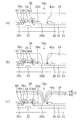
本発明による実施形態1の液晶表示装置100の模式的な構造を図1(a)および(b)に示す。図1(a)は液晶表示装置100の模式的な断面図であり、図1(b)は模式的な平面図である。液晶表示装置100は、TFTを用いたアクティブマトリクス型の反射型液晶表示装置である。
【0041】
液晶表示装置100は、反射電極基板100aと、対向基板100bと、反射電極基板100aと対向基板100bとの間に設けられた液晶層60とを有している。液晶層60は、シール部62によって、両基板100aおよび100bの間に封入されている。
【0042】
反射電極基板100aは、例えばガラスからなる基板10上に反射電極12を有している。反射電極12は、Al層(Alを含む金属層)14とその直下に形成されたMo層(Moを含む金属層)16とを有する。この反射電極12の構成をAl層/Mo層の2層構造と呼ぶこともある。図1に示された反射電極12は、後述するように、マトリクス状に配置され、それぞれがTFT(不図示)に接続された複数の絵素電極を模式的に示したものである。この反射電極12は、周囲光を適度な角度分布で拡散反射(「散乱」ということもある)するように、その表面の断面が波状(凹凸)になるように形成されている。ここでは、表面が波状の樹脂層18を形成し、樹脂層18の表面上に、Mo層16およびAl層14を順次形成することによって、波状の表面を有する反射電極12を形成している。反射電極12が有するMo層16の表面のMoの最大粒径は60nm以下であり、その上に形成されているAl層14は設計どおりの面積と膜厚を有し、設計どおりの反射特性を有している。この反射電極12の構成およびその形成方法については、後に詳述する。
【0043】
対向基板100bは、例えばガラスからなる透明基板50上(液晶層60側)に、ITO(インジウム錫酸化物)などから形成された透明な対向電極52を有している。対向電極52は、複数の反射電極(絵素電極)12に対向する単一の共通電極である。対向電極52および反射電極12の表面にはそれぞれ配向膜(不図示)が設けられており、液晶層60の液晶分子(不図示)は90°ツイスト配向している。また、TNモードで表示を行うために、対向基板100bの観察者側(液晶層60とは反対側)には、4分の1波長(λ/4)板72および偏光板74が設けられている。また、必要に応じて、カラーフィルタ層(不図示)が形成される。
【0044】
液晶表示装置100は、対向電極52とそれぞれの反射電極12との間に印加される電圧によって液晶層60の液晶分子の配向状態が変化し、この配向状態の変化に対応して、反射光の強度が変調され表示が行われる。対向電極52とそれぞれの反射電極12とが対向する領域が絵素領域(表示の最小単位である絵素に対応する領域)を規定する。なお、ブラックマトリクスを形成した場合には、ブラックマトリクスの開口部が絵素領域を規定する。
【0045】
液晶表示装置100において、複数の絵素領域を含み、表示を行う領域を表示領域10Aと称し、表示領域10Aの周辺部に位置し、TFTに電圧を供給するための走査線や信号線(いずれも不図示)の端子電極が形成される領域を端子領域10Tと称する。なお、後述するように、本発明によるAl層/Mo層の2層構造を有する反射電極12およびその形成方法は、この端子電極の形成においても、効果を奏する。端子電極の最上層は酸化による接触抵抗の上昇を防止するためにITO層で形成される。液晶表示装置100の製造プロセスにおいて、このITO層上にAl層が一時的に形成され、そのAl層をパターニングする必要が生じると、Alとの電食によってこのITO層の一部が欠落することがある。後述するように、本発明によるAl層/Mo層の2層構造を有する反射電極12を用いることによって、端子電極のITO層の欠落の問題を防止することができる。
【0046】
図2(a)および(b)を参照しながら、反射電極12の構造およびその形成方法を詳細に説明する。図2(a)は、液晶表示装置100の反射電極基板100aの一絵素領域の平面図であり、図2(b)は図2(a)中の2B−2B’線に沿った断面図である。
【0047】
反射電極基板100aは、図2(a)に示したように、基板10上に、互いに平行な複数の走査線(ゲートバスライン)22と、走査線22に交差し、互いに平行な複数の信号線(ソースバスライン)24と、走査線22と信号線24とがそれぞれ交差する付近に設けられた複数のTFT26を有し、それぞれのTFT26に反射電極12が接続されている。
【0048】
図2(b)に示したように、基板10上に、走査線およびゲート電極(一般にこれらは一体に形成されるので同一の参照符号で示す。)22が形成されている。走査線およびゲート電極22を覆うゲート絶縁層32が形成されており、ゲート絶縁層32上に、半導体層34、ソースコンタクト層36sおよびドレインコンタクト層36d、ソース電極38sおよびドレイン電極38dが形成され、TFT26が構成されている。このTFT26を覆うように、ほぼ全面にパッシベーション層40が形成されている。さらに、パッシベーション層40を覆うように、波状の表面を有する樹脂層18が形成されており、樹脂層18上に反射電極12が形成されている。
【0049】
なお、ソースコンタクト層36sとソース電極38sとの間およびドレインコンタクト層36dとドレイン電極38dとの間に、それぞれITOから形成された電極30sおよび30dが形成されている。ドレイン側の電極(接続電極とも言う。)30dは、樹脂層18に設けられたコンタクトホール18aおよびパッシベーション層40に設けられたコンタクトホール40a内で、反射電極12と互いに電気的に接続されている。
【0050】
反射電極12以外の構成要素は、公知の材料を用いて公知の方法で形成することができる。例えば、走査線およびゲート電極22、信号線24、ソース電極38sおよびドレイン電極38dは、Taを用いて形成されるが、これに限られず、所望の配線抵抗が得られる材料(金属、ドープされた半導体、これらの積層体)であればよいし、Mo層16と良好なオーミック性接触が取れる材料であるならば、コンタクトホール40a内にドレイン電極38dを露出させてもよい。また、例えば、ゲート絶縁層32は酸化シリコンで、半導体層34はa−Siで、ソースコンタクト層36sおよびドレインコンタクト層36dはn+ −Siで、パッシベーション層40は窒化シリコン(SiNx )などを用いて形成することができる。製造方法としては、成膜工程、フォトリソグラフィ工程、エッチング工程、およびレジスト剥離工程を繰り返す方法を例示することができる。あるいは、連続成膜、一括エッチング等の製造方法を用いることもできる。
【0051】
以下の製造工程を図3(a)〜(c)を参照しながら説明する。
【0052】
図3(a)に示したように、上述のようにしてTFT等が形成された基板10の表面を覆うように、樹脂層18を形成する。TFT26およびパッシベーション層40が形成された基板10上に、例えば、ポジ型感光性樹脂(例えば、東京応化工業(株)製: 商品名OFPR−800)を所望の膜厚(例えば1.5μm)が得られるように塗布する。
【0053】
次に、この基板10を約100℃で約30秒間プリベークした後、図4(b)に示したフォトマスク80bを介して、400mJで露光(高照度露光)し、その後、図4(a)に示したフォトマスク80aを介して180mJで露光(低照度露光)し、合計2回露光する。なお、この2回の露光工程の順序は逆でもよい。
【0054】
図4(a)および(b)に示したフォトマスク80aおよび80bは、それぞれ、遮光部82aおよび82bと、透光部84aおよび84bとを有している。図4(a)および(b)は、いずれも一絵素に相当する部分を模式的に示している。図4(a)のフォトマスク80aの遮光部82aは反射電極の全体の面積の約20%〜40%の範囲にあることが好ましく、隣接する遮光部82aの中心の間隔は、約5μm〜約50μmの範囲内にあることが好ましく、約10μm〜約20μmの範囲内にあることがさらに好ましい。各遮光部82aの中心位置は、面内にランダムに配置されている。遮光部82aの形状は、図示した円形に限られず、多角形でもよい。図4(b)のフォトマスク80bが有する透光部84bはコンタクトホール18aおよび40aを形成するためのものである。また、フォトマスク80bは、反射電極基板100a上の端子電極部(走査線端子電極部および信号線端子電極部)に対応する位置にも透光部(不図示)を有している。
【0055】
次に、露光されたポジ型感光性樹脂を現像液(例えば、東京応化工業(株)製のTMA(テトラメチルアンモニウムハイドロオキサイド))を用いて現像することによって、フォトマスク80bの透光部に対応するコンタクトホール形成部および端子電極に対応する高照度露光部の感光性樹脂が除去され、フォトマスク80aの透光部84aに対応する低照度露光部の感光性樹脂は初期膜厚の約40%が残存し、フォトマスク80aの遮光部82aに対応する未露光部分の感光性樹脂は初期膜厚の約80%が残存する。
【0056】
その後、90℃にて1分仮焼きした後、約200℃で約60分の熱硬化処理を行うことによって、熱だれ現象によって感光性樹脂層の断面形状が変形し、滑らかな凹凸形状の表面が形成される。
【0057】
このようにして、図3(b)に示したように、波状の表面を有する樹脂層18と、反射電極12を接続電極30dに電気的に接続するためのコンタクトホール18aとを形成した。なお、この後の反射電極12を形成する前に、O2 プラズマによるディスカム処理(スカムを除去する処理)を行ってもよい。また、樹脂層18に波状の表面を形成するためのフォトマスク80aを介した露光工程における露光量を180mJとしたが、液晶表示装置のパネルサイズにより要求される散乱特性(拡散反射光の角度分布)が異なるので、露光量は適宜変更され得る。反射電極基板100aを製造する方法として、上記の例の他に、例えば、特開平6−75238号公報に開示されている方法を採用することができる。
【0058】
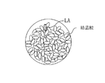
次に、図3(c)に示したように、上述のようにして得られた基板上に、Mo層16とAl層14との2層構造を有する反射電極12を形成する。ここでは、本実施形態1の具体例として、Mo層16の表面粒径が30nm以下(具体例1)と、表面粒径が60nm以下(具体例2)の結晶層を形成した例を示し、さらに、比較のために、表面粒径が90nm以下(比較例1)のMo層を形成した。Mo層16の成膜は、全て同一のスパッタリング装置を用いて実行した。それぞれのMo層16の堆積条件および、得られたMo層16の表面を光学顕微鏡または電子顕微鏡を用いて観察した結果得られた最大粒径を下記の表1に示す。表面観察で得られるMo層16の表面の形態を模式的に図5に示す。図5に示したように、Moの柱状結晶は楕円状に観察される。この楕円の長軸LAの長さを粒径とし、それぞれのMo層16の表面における最大粒径を求めた。なお、最大粒径は、基板の中心部とその周辺部とにおいて、それぞれ2.3μm×1.7μmの範囲内で表面観察を行って求めた。
【0059】

このようにして得られたそれぞれのMo層16上にスパッタリング法を用いてAl層14を堆積した。Al層14の堆積条件は、いずれも同じで、雰囲気圧力0.2Pa、投入電力10KW、膜厚100nmとした。表面の粒径が60nmとなるようにMo層16の堆積条件を決定すれば、Al層14の堆積工程は、Mo層16の堆積工程に引き続いて、スパッタリング装置の真空を破ることなく、連続的に実行することができる。得られたAl層14中に発生したピンホールの数密度を顕微鏡観察から求めた。Al層14中のピンホールの数密度は、典型的な絵素の大きさに対応する100μm×100μmの範囲内の数で求めた。
【0061】
具体例1のMo層16上に形成されたAl層14にはピンホールが観察されず、具体例2のMo層16上に形成されたAl層14のピンホールの数密度は、5〜10個/10000μm2 であった。一方、比較例1のMo層上に形成されたAl層には、200〜300個/10000μm2 ものピンホールが形成されていた。
【0062】
このようにして形成されたMo層16およびAl層14をパターニングすることによって、図2(b)に示した所定の形状の反射電極12を形成した。Mo層16およびAl層14のパターニングは、以下のようにして行った。
【0063】
まず、通常のフォトリソグラフィプロセスで、所定の形状にパターニングされたレジスト層を形成する。このレジスト層をマスクとし、酢酸、燐酸および硝酸を水に混合した混酸をエッチャントとして用いて、レジスト層から露出されたMo層16およびAl層14を一括で除去した。
【0064】
その後、マスクとして用いたレジスト層をアルカリ系剥離液(例えば、東京応化工業(株)製の剥離液106(商品名))を用いて除去した。
【0065】
具体例1、2および比較例1のそれぞれについて、形成された反射電極12を光学顕微鏡または電子顕微鏡を用いて観察した結果および反射率を測定した結果を、合わせて下記の表2に示す。なお、反射率は、堆積したまま(パターニング前)のAl層14の反射率に対する低下率で評価した。
【0066】
Mo層16中にピンホールが生成されなかった具体例1では、反射電極12(Al層14)に欠けが発生せず、反射率の低下も無かった。また、具体例2では、反射電極12のエッジ部がガタガタになるエッジ欠け及び後述する円形欠けが発生したが、反射率の低下は認められなかった。これに対し、比較例1では、Al層中のピンホールを中心に直径が2〜5μmの円形の欠けが観察されるとともに、反射率が8〜13%低下した。これらの反射電極基板100aを用いて、図1に示した反射型液晶表示装置100を作製し、表示特性を評価した結果、比較例1の液晶表示装置は、具体例1および具体例2の液晶表示装置100に比べ、10%程度反射率が低かった。
【0068】
上述の結果から、Mo層16の表面のMo粒径とAl層14中のピンホール発生数との相関が確認され、Mo層の表面粒径が60nm以下であれば、実用上の問題が無く、表面粒径が30nm以下であれば、ピンホールの発生が無く、良好な反射特性を有する反射電極を形成できることが分かった。
【0069】
また、図2(b)に示したように、反射電極12の一部をITO層から形成された接続電極30d上に直接形成する構造において、本発明によるAl層14/Mo層16の2層構造を採用すると、上述した反射電極12のパターニングやレジスト剥離工程において、接続電極30dのITO層が電食によって欠落することを防止することができる。
【0070】
さらに、本発明によるAl層/Mo層の2層構造を採用すると、以下に説明するように、反射電極基板100aの端子電極の最上層として形成されるITO層がAlとの電食によって欠落することを防止できる利点もある。
【0071】
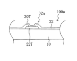
反射電極基板100aの表示領域(図1中の10A)内の配線(走査線)に接続され、端子領域(図1中の10T)内に形成される走査線端子電極22Tの断面構造を図6に模式的に示す。図示しないが、表示領域内の信号線に接続される信号線端子電極も同様の構造を有している。図6に示した走査線端子電極22Tは、基板10上に走査線およびゲート電極22と一体に形成される。この走査線端子電極22Tを覆うように形成されたゲート絶縁層32には、開口部32aが形成されており、開口部32a内で走査線端子電極22Tに電気的に接続されるようにITO層30Tが形成されている。ITO層30Tは、走査線端子電極22Tの表面が空気によって酸化されるのを防止し、低い接続抵抗を維持することができる。このITO層30Tは、例えば、上述した接続電極30dと同一工程で形成される。
【0072】
反射電極基板100aの製造プロセスにおいては、このITO層30T上にも一時的に反射電極12を形成するための層(Mo層16およびAl層14)が形成される。従って、従来のように、Al層14を直接ITO層30T上に形成すると、Al層14を除去する工程で、AlとITOとの電食によってITO層30Tの一部が欠落する問題が発生する。しかしながら、本発明によるAl層/Mo層の2層構造を採用すると、ITO層30Tが電食によって欠落することを防止できる。
【0073】
図7(a)〜(c)を参照しながら、走査端子電極22Tの形成工程を説明する。図7(a)、(b)および(c)は、ぞれぞれ、図3(a)、(b)および(c)に示した各工程における走査線端子電極部の断面構造を示している。
【0074】
図7(a)に示したように、ITO層30Tを最上層に有する走査線端子電極部を覆うように、樹脂層18を形成するためのポジ型感光性樹脂が塗布される(図3(a)参照)。
【0075】
このポジ型感光性樹脂を露光・現像することによって、図7(b)に示したように、ITO層30Tを最上層とする走査線端子電極部が露出される(図3(b)参照)。すなわち、ポジ型感光性樹脂を露光する工程で用いられるフォトマスク80bは、走査線端子電極部に対応する位置に透光部を有している。
【0076】
次に、図7(c)に示したように、ITO層30Tが露出された基板10の全体を覆うように、反射電極12を形成するためのMo層16とAl層14とが一時的に堆積される。この後、図3(c)を参照しながら上述したように、レジストを用いたフォトリソグラフィプロセスで、Mo層16とAl層14とからなる2層構造を有する反射電極12が所定の形状にパターニングされるとき、走査線端子電極部を覆うMo層16およびAl層14が一括で除去される。
【0077】
本発明によると、ITO層30T上にはMo層16を介してAl層14が形成されているので、反射電極12を形成するためのパターニング工程(Mo層16およびAl層14のエッチング工程)において、ITO層30TにAl層14が直接に接触することがないので、ITOとAlとの電食によるITO層30Tの部分的な欠落の発生を防止することができる。
【0078】
上述したように、本発明の実施形態によると、反射電極12の形成工程において、ピンホールによるAl層の部分的な欠落が防止され、且つ、反射電極12がITO層上に形成される場合には、ITOとAlとの電食によるITO層およびAl層の部分的な欠落が防止される。さらに、端子電極の最上層にITO層を有する構成を採用した場合は、端子電極のITO層上に一時的に形成されるAl層を除去する工程において、ITOとAlとの電食によってITO層が部分的に欠落することが防止できる。従って、設計どおりの反射特性を有する反射電極を形成できるとともに、信頼性の高い端子電極を形成することができる。
【0079】
本実施形態においては、端子電極の最上層にITO層を有する構成を例示したが、本発明はこの例に限られず、表示領域内に形成される配線や電極の最上層にITO層を有する構成においても、同様に作用効果を奏する。
【0080】
また、本実施形態では、Mo層16として純Mo層を、Al層14として純Al層を用いたが、これらに限られず、それぞれ他の金属が少量添加されても本発明の効果を得ることができる。添加される金属の種類および量は、電気特性(比抵抗など)やパターニング性等を考慮して適宜設定され得る。また、本実施形態では、ポジ型レジストを用いて樹脂層18を形成したが、ネガ型レジストを用いることもできる。また、別途レジストを用いてコンタクトホールの形成や波状の表面を形成する必要が生じるが、非感光性の絶縁材料を用いて樹脂層を形成してもよい。これらのことは、下記の実施形態2についても同様である。
【0081】
また、Mo層16の結晶粒の成長の仕方は、下地層の材料に依存する。下地層の材料によっては、Mo結晶粒が明確な柱状結晶とならない場合もあるが、Mo層16の表面の結晶粒の最大粒径が60nm以下であれば本発明の効果を得ることができる。
【0082】
(実施形態2)
本実施形態では、Mo層16をスパッタリング法で成膜する工程を窒素ガスを含有する雰囲気下で行うことによって、アモルファスMoからなるMo層16を形成する。アモルファスMoからなるMo層16を形成すること以外は、実施形態1と同じなので、その詳細な説明はここでは省略する。
【0083】
アモルファスMoからなるMo層16は、例えば、投入電力を10KW、雰囲気圧力を0.5Paとし、膜厚が50nmのMo層を堆積する工程を、流量20sccmで窒素(N2 )ガスを流しながら実行することによって、形成することができる。アモルファスMoからなるMo層16の表面を光学顕微鏡または電子顕微鏡で観察すると、実施形態1の具体例1のMo層16の表面(粒径30nm以下)よりも小さな構造しか観察されなかった。これは、アモルファス相は、数原子単位で結合手が繋がった構造を有し、結晶粒を実質的に含まないからである。
【0084】
得られたMo層16上に、実施形態1と同様にして、Al層14を成膜し、Al層14/Mo層16をパターニングした後、レジスト剥離を行った。得られたAl層14にはピンホールは観察されず、反射率の低下も認められなかった。このようにして得られた反射電極12を有する液晶表示装置100は、実施形態1の具体例1と同様に、優れた表示特性を示した。また、上記の窒素雰囲気下で堆積されたMo層16は、窒素元素を僅かに含むが、電気抵抗の低下による表示特性の低下も見られなかった。なお、本実施形態2のMo層16は、窒素ガス流量を20sccmとして成膜したが、窒素ガス流量はこれに限られず、所望する抵抗以下のMo層16が形成される範囲内で適宜調整され得る。
【0085】
上述の実施形態1および2中で用いた成膜条件は、本願発明者が使用したスパッタリング装置を用いた場合の条件であり、使用するスパッタリング装置の仕様(例えば、チャンバー容積等)等により変わり得るものであり、上記の数値に限定されるものでは無い。
【0086】
(実施形態3)
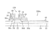
本発明による実施形態3の液晶表示装置として、TFTを用いたアクティブマトリクス型の透過型液晶表示装置について説明する。本実施形態によるTFT基板200aの模式的な断面図を図8に示す。TFT基板200aにおいて、信号線、ソース電極およびドレイン電極は、ITO層から形成された透明導電層、Mo層16およびAl層14が順次積層された構造をそれぞれ有する。
【0087】
なお、本実施形態および実施形態4において、デバイスの一構成要素としてパターニングされた後のITO層を特に透明導電層と言う。ITO層をパターニングしてソース電極およびドレイン電極を形成したときのソース電極側の透明導電層を30sと表記し、ドレイン電極側の透明導電層を30dと表記する。透明導電層30dのうちMo層16およびAl層14に覆われていない部分は、絵素電極として機能する。ソース電極側の透明導電層30s、Mo層16およびAl層14は、図8の紙面に対して垂直方向に延びて信号線(ソースバスライン)を形成する。
【0088】
図8に示すTFT126の形成工程のうち、半導体層34の形成工程までは実施形態1と同様であり、実施形態1と同様の成膜工程、フォトリソグラフィ工程、エッチング工程、およびレジスト剥離工程を繰り返すことによって、基板10上に走査線、ゲート電極22、ゲート絶縁層32、半導体層34、ソースコンタクト層36s、ドレインコンタクト層36dをそれぞれ形成することができる。
【0089】
半導体層34が形成された基板10上に、スパッタリング装置などによって、ITO層を100nm厚程度堆積する。本実施形態の具体例3、4および比較例2として、実施形態1と同様の成膜条件下、表面粒径が30nm以下(具体例3)、60nm以下(具体例4)および90nm以下(比較例2)をそれぞれ有するMo層16をスパッタリング法にて成膜した。次に、スパッタリング法などによって、Mo層16上にAl層14を成膜する。本実施形態の具体例3、4および比較例2では、実施形態1と同様の条件下、スパッタリング法によって、100nm厚程度のAl層14を成膜した。
【0090】
以下、TFT126のソース電極側の透明導電層30s、Mo層16およびAl層14のパターニングについて、図9を参照しながら説明する。図9(a)〜(g)は、TFT126のソース電極側の透明導電層30s、Mo層16およびAl層14のパターニング工程を説明するための模式的な断面図である。なお、ソース電極側の透明導電層30sがパターニングされる前のITO層を130と表記する。また、図9以降において、図8に記載された基板10、ゲート電極22および半導体層34の記載を省略する。
【0091】
ITO層130、Mo層16およびAl層14が順次積層された基板(図9(a)参照)上にレジストを塗布し、フォトリソグラフィ工程によって、Mo層16およびAl層14をパターニングするためのレジストパターン(以下、Al層/Mo層パターニング用レジストパターンともいう。)150を形成する(図9(b)参照)。Al層/Mo層パターニング用レジストパターン150をマスクとし、酢酸、燐酸および硝酸を水に混合した混酸をエッチャントとして用いて、レジストパターン150から露出されたMo層16およびAl層14を一括で除去する(図9(c)参照)。この後、アルカリ系剥離液を用いてレジストパターン150を除去する(図9(d)参照)。
【0092】
次に、得られた基板のほぼ全面にレジストを塗布し、フォトリソグラフィ工程によって、ITO層130をパターニングするためのレジストパターン(以下、ITO層パターニング用レジストパターンともいう。)151を形成する。このITO層パターニング用レジストパターン151は、既にパターニングされたMo層16およびAl層14のエッジ部が露出しないように、Mo層16およびAl層14を覆う(図9(e)参照)。ITO層パターニング用レジストパターン151をマスクとし、塩化第二鉄および塩酸の混合液をエッチャントとして用いて、レジストパターン151から露出されたITO層130を除去する(図9(f)参照)。この後、アルカリ系剥離液を用いてレジストパターン151を除去して、透明導電層30s、Mo層16およびAl層14が順次積層された構造を有するソース電極を形成する(図9(g)参照)。
【0093】
なお、図示しないが、ソース電極の形成とともに、ソース電極側の透明導電層30s、Mo層16およびAl層14が順次積層された構造を有する信号線(ソースバスライン)が形成され、ドレイン電極側の透明導電層30d、Mo層16およびAl層14が順次積層された構造を有するドレイン電極が形成される。さらに、ドレイン電極側の透明導電層30dのうちMo層16およびAl層14が除去された部分が絵素電極となる。
【0094】
本実施形態においては、Mo層16を介してAl層14が透明導電層30d上に設けられているので、透明導電層30d上のAl層14を除去して絵素電極を形成するとき、エッチャントまたはアルカリ系の現像液や剥離液によるITOとAlとの電食が防止され、透明導電層30dの部分的な欠落の発生を防止することができる。
【0095】
本実施形態のパターニング工程では、ITO層パターニング用レジストパターン151がMo層16およびAl層14のエッジ部が露出しないように、Mo層16およびAl層14を覆っているので、ITO層130をエッチングする際にMo層16およびAl層14がエッチャントに接触しない。したがって、Mo層16およびAl層14のエッジ部は、レジストパターン151のエッジ部から線幅が細くなる方向に過度にエッチングされない。
【0096】
以上のパターニング工程の後、基板上にパッシベーション層40を堆積し、フォトリソグラフィ工程によるパターニングを行なって、図8に示されたTFT基板200aが形成される。本実施形態の具体例3、4および比較例2により得られた3種のTFT基板を用いて、公知の方法にて透過型のTN型液晶表示装置(各100パネル)をそれぞれ作製した。各具体例および比較例の液晶表示装置について、信号線断線が発生したパネル数を計数した。また、各具体例および比較例の液晶表示装置について、全パネルの輝点数を総計し、輝点数を100で除して1パネル当たりの輝点数(個/パネル)を算出した。これらの結果を表3に示す。
【0097】
比較例2の液晶表示装置に関して、断線原因の調査を行なったところ、19パネルに関してはAl層のピンホールの拡大が原因であった。比較例2の信号線はMo層の表面粒径が90nm以下であり、Mo層上に形成されたAl層中のピンホールの数密度が高いので、エッチャントやアルカリ系剥離液などによるAl層中のピンホールの拡大に起因して生じるAl層およびMo層の欠落の程度が大きく、断線が生じ易いと考えられる。
【0099】
これに対して、具体例3および4では、Mo層16の表面粒径が30nm以下(具体例3)または60nm以下(具体例4)であり、Mo層16上に形成されたAl層14中のピンホールの数密度が低いので、Al層14中のピンホールの拡大に起因するAl層14およびMo層16の欠落の程度が小さく、断線が生じ難いと考えられる。本実施形態では、アルカリ系剥離液によるレジストパターン150および151の除去を2回行なっているので、Al層14がアルカリ系剥離液に接触する時間が長くなり、Al層中のピンホールの拡大が生じ易い条件下でパターニングが行われている。それにもかかわらず、本実施形態によれば、断線が生じ難く、歩留りが向上するという効果が得られる。
【0100】
本実施形態の具体例においては、Mo層16の表面粒径が30nm以下(具体例3)または60nm以下(具体例4)について説明したが、Mo層16としてアモルファスMoからなるMo層を用いても良く、また実施形態1において説明した積層構造のMo層を用いても良い。アモルファスMoからなるMo層や積層構造のMo層を用いても、上記と同様の効果を奏する。本実施形態においては、Mo層16およびAl層14を除去した後、アルカリ系剥離液を用いてAl層/Mo層パターニング用レジストパターン150を除去しているが(図9(d)参照)、レジストパターン150を除去しない状態で、ITO層パターニング用レジストパターン151の形成、ITO層130のエッチングを順次行なった後、両レジストパターン150および151を一括して除去することも可能である。
【0101】
(実施形態4)
本実施形態の液晶表示装置は、実施形態3のものと同じであるが、透明導電層30sおよび30d、Mo層16ならびにAl層14のパターニンク工程が実施形態3と異なり、ITO層130をパターニングした後の透明導電層30sおよび30d上に、Al層/Mo層の2層を堆積し、Al層/Mo層のパターニングを行なう。以下、図10を参照しながら、本実施形態によるパターニング工程を説明するが、ITO層130を堆積する工程までは実施形態3と同じであるから、ITO層130を堆積する工程までについては説明を省略する。
【0102】
図10(a)〜(f)は、TFT126のソース電極側の透明導電層30s、Mo層16およびAl層14のパターニング工程の他の例を説明するための模式的な断面図である。まず、基板のほぼ全面にレジストを塗布し、フォトリソグラフィ工程によって、ITO層パターニング用レジストパターン151を形成する(図10(b)参照)。レジストパターン151をマスクとし、塩化第二鉄および塩酸の混合液をエッチャントとして用いて、レジストパターン151から露出されたITO層130を除去する。その後、アルカリ系剥離液を用いてレジストパターン151を除去する(図10(c)参照)。
【0103】
次に、Mo層16およびAl層14を順次スパッタリング法にて成膜する(図10(d)参照)。基板上にレジストを塗布し、フォトリソグラフィ工程によって、Al層/Mo層パターニング用レジストパターン150を形成する(図10(e)参照)。レジストパターン150をマスクとし、酢酸、燐酸および硝酸を水に混合した混酸をエッチャントとして用いて、レジストパターン150から露出されたMo層16およびAl層14を一括で除去する。このとき、透明導電層30sを構成するITOは上記混酸に対して溶解され難いので、透明導電層30sの線幅の狭小または断線が生じる可能性は低い。Al層14およびMo層16をパターニングした後、アルカリ系剥離液を用いてレジストパターン150を除去する。
【0104】
実施形態3と同様に、本実施形態の具体例により得られたTFT基板を用いて、透過型のTN型液晶表示装置を作製した。作製された液晶表示装置について、実施形態3と同様に、信号線断線が発生したパネル数、1パネル当たりの輝点数を求めたところ、実施形態3と同様の結果となった。
【0105】
本実施形態においても、実施形態3と同様に、Mo層16の表面粒径が60nm以下であり、Mo層16上に形成されたAl層14中のピンホールの数密度が低いので、Al層14中のピンホールの拡大によるAl層14およびMo層16の欠落の程度が小さく、断線が生じ難いと考えられる。本実施形態では、アルカリ系剥離液によるレジストパターン150および151の除去を2回行なっているので、Al層14がアルカリ系剥離液に接触する時間が長くなり、Al層中のピンホールの拡大が生じ易い条件下でパターニングが行われている。それにもかかわらず、本実施形態によれば、断線が生じ難く、歩留りが向上するという効果が得られる。
【0106】
実施形態3および4においては、ITO層130とAl層14/Mo層16とを、それぞれ別のフォトリソグラフィ工程およびエッチング工程によってパターニングしているが、ITO層130とAl層14/Mo層16とを別途パターニングすることは本発明の液晶表示装置の製造方法において必要不可欠な事項ではない。例えば、実施形態3において、Al層/Mo層パターニング用レジストパターン150を形成した後、酢酸、燐酸および硝酸を水に混合した混酸によるエッチングを行ない、レジストパターン150を剥離することなく、塩化第二鉄および塩酸の混合液によるエッチングを行なってもよい。
【0107】
しかしながら、塩化第二鉄および塩酸の混合液に浸したとき、AlおよびMoはITOよりも速い(特にMoは非常に速い)スピードで溶解するので、Al層14/Mo層16のサイドエッチングがITO層130よりも激しくなり、図11に示すように、Al層14/Mo層16のエッジ部が著しく後退するおそれがある。したがって、Al層/Mo層の狭小化によって、ソース・ドレインの間隔、バスラインなどの線幅を制御することが困難となる。
【0108】
実施形態3および4によれば、ITO層パターニング用レジストパターン151によってAl層14/Mo層16が覆われているか、あるいはITO層130をエッチングした後にAl層14/Mo層16が形成されるので、Al層14/Mo層16が塩化第二鉄および塩酸の混合液に接触しない。したがって、実施形態3および4によれば、ソース・ドレインの間隔、バスラインなどの線幅を制御することが容易となる。
【0109】
上記の実施形態1および2では、反射型液晶表示装置を例に本発明による実施形態を説明したが、本発明はこれに限られず、透過反射両用型の液晶表示装置(特開平11−101992号公報参照)のように絵素電極の一部が反射電極(反射層)である場合にも適用できる。また、本発明の液晶表示装置は、例示したTFTを用いたアクティブマトリクス型液晶表示装置に限られず、MIM素子を用いたアクティブマトリクス型液晶表示装置や単純マトリクス型液晶表示装置に適用してもよい。さらに、表示モードも例示するTNモードに限られず、反射光を利用した表示が可能な公知の表示モード(例えば、ゲスト−ホストモードのような光吸収モード、高分子分散型液晶表示装置のような光散乱モード、STNモードのようなECBモード、強誘電性液晶モードなど)を広く利用することができる。
【0110】
上記の実施形態3および4では、信号線、ソース電極およびドレイン電極のいずれもが、ITO層から形成された透明導電層、Mo層およびAl層が順次積層された構造を有する場合について説明したが、本発明においては信号線、ソース電極およびドレイン電極のうち少なくとも1つがAl層/Mo層/透明導電層の3層構造を有していれば良い。また、実施形態3および4では、絵素電極がゲート絶縁層上に形成された透過型液晶表示装置について説明したが、本発明はこれに限られず、TFTを覆う透明な有機絶縁層がゲート絶縁層上に設けられ、この有機絶縁層上に絵素電極が形成された高開口率構造の透過型液晶表示装置に応用することもできる。
【0111】
本発明の配線・電極基板は、液晶表示装置以外の表示装置、例えば有機ELを用いた表示装置などに適用することができ、さらに、太陽電池などにも適用することができる。有機ELを用いた表示装置および太陽電池において、光の制御および利用に関わる電極として、ITOから形成された透明導電層が用いられ、さらに透明導電層の電気伝導度を補うために、AlまたはAl合金の層が透明導電層上の一部の領域に堆積される。本発明の配線・電極基板によれば、基板上に設けられた多層構造の配線または電極におけるAl層の幅が狭くなり過ぎたり、Al層の断線が発生するのを抑制・防止することができる。したがって、本発明の配線・電極基板を有機ELを用いた表示装置や太陽電池などに用いることによって、配線または電極の電気伝導度が低下することを抑制・防止し、不良品の発生を抑えることができる。
【0112】
【発明の効果】
本発明によると、Mo層上に形成されたAl層にピンホールが発生するのが抑制・防止されるので、Al層中のピンホールに起因するAl層の欠落の発生が抑制・防止される。したがって、反射層として機能するAl層が、製造プロセスにおいて欠落することを抑制・防止することができるので、設計どおりの反射特性を有する液晶表示装置を製造することができる。
【0113】
また、Al層/Mo層/透明導電層の3層構造を有する配線もしくは電極の電気伝導度の低下または断線の発生を抑制・防止することができるので、不良品の発生を抑え、歩留りが向上するという効果を奏する。
【0114】
さらに、ITO層上に一時的に形成されたAl層を除去する場合においても、本発明によるAl層/Mo層の2層構造を適用することによって、ITOとAlとの電食に起因するITO層の欠落を防止することができる。したがって、端子電極の最上層のITO層上に一時的に堆積されたAl層を剥離する際に生じ得るITO層の欠落の発生が抑制・防止され、信頼性の高い端子電極を形成することができる。
【図面の簡単な説明】
【図1】本発明による実施形態1の液晶表示装置100を模式的に示す図であり、(a)は断面図、(b)は平面図である。
【図2】実施形態1の液晶表示装置100の反射電極基板100aを模式的に示す図であり、(a)は平面図、(b)は断面図である。
【図3】(a)〜(c)は、実施形態1の液晶表示装置100の反射電極基板100aの製造プロセスを模式的に示す断面図である。
【図4】(a)および(b)は、実施形態1の液晶表示装置100の製造に用いれるフォトマスクの例を示す模式図である。
【図5】実施形態1で形成されるMo層16の顕微鏡観察結果を模式的に示す図である。
【図6】実施形態1の液晶表示装置100の走査線端子電極22Tの模式的な断面図である。
【図7】(a)〜(c)は、実施形態1の液晶表示装置100の走査線端子電極22Tの製造プロセスを模式的に示す断面図である。
【図8】実施形態3によるTFT基板200aを模式的に示す断面図である。
【図9】(a)〜(g)は、実施形態3によるTFT126のソース電極側の透明導電層30s、Mo層16およびAl層14のパターニング工程を説明するための模式的な断面図である。
【図10】(a)〜(f)は、実施形態4によるTFT126のソース電極側の透明導電層30s、Mo層16およびAl層14のパターニング工程の他の例を説明するための模式的な断面図である。
【図11】他の実施形態によるTFT126のソース電極側の透明導電層30s、Mo層16およびAl層14のエッチング後の状態を示す模式的な断面図である。
【符号の説明】
10、50 基板(ガラス基板)
10A 表示領域
10T 端子領域
12 反射電極
14 Al層
16 Mo層
18 樹脂層
18a、40a コンタクトホール
22 走査線(ゲートバスライン)、ゲート電極
22T 走査線端子電極
24 信号線(ソースバスライン)
26、126 TFT
30s、30d、30T 電極(ITO層)
32 ゲート絶縁層
32a 開口部
34 半導体層
36s、36d コンタクト層
38s、38d 電極(Ta層)
40 パッシベーション層
52 対向電極(透明電極)
60 液晶層
62 シール部
72 λ/4板
74 偏光板
80a、80b フォトマスク
82a、82b 遮光部
84a、84b 透光部
100 液晶表示装置
100a 反射電極基板
130 ITO層
200a TFT基板[0001]
BACKGROUND OF THE INVENTION
The present invention relates to a liquid crystal display device, a wiring board, and a manufacturing method thereof, and more particularly to a liquid crystal display device capable of performing display in a reflection mode using ambient light and a manufacturing method thereof.
[0002]
[Prior art]
In recent years, application of liquid crystal display devices to word processors, laptop personal computers, pocket televisions, and the like is rapidly progressing. In particular, a reflective liquid crystal display device capable of performing display by reflecting ambient light among liquid crystal display devices does not require a backlight, and thus has low power consumption, is thin, and can be reduced in weight. Because of it. Recently, a dual-use liquid crystal display device capable of displaying in both the reflection mode and the transmission mode has also been developed.
[0003]
In order to reflect ambient light, a reflection plate or a reflection layer has conventionally been provided outside the substrate of the liquid crystal display device (TFT substrate or a substrate provided on the side opposite to the observer). When the picture element size is reduced with the increase in capacity of the liquid crystal display device, in such a structure, the display quality is deteriorated due to the parallax caused by the difference in the distance between the color filter (pixel portion) and the reflection plate (reflection layer). The problem arises.
[0004]
In order to solve this problem, a reflective layer is provided on the liquid crystal layer side of the substrate, and the reflective layer itself is an electrode for applying a voltage to the liquid crystal layer (for example, a pixel electrode in a TFT type liquid crystal display device). The configuration to be used as is now widely used. As a material for forming the reflective layer, Al (and an Al alloy) is often used because it has high reflectivity, excellent patternability, and low electrical resistance.
[0005]
On the other hand, if they are exposed to an alkaline solution in a state where the ITO layer and the Al layer are in contact with each other, electrolytic corrosion occurs between the ITO and Al, and a part of the ITO layer and the Al layer is lost. Is known to occur. In the following description, unless otherwise specified, the term “ITO layer” means not only an ITO layer before patterning but also an ITO layer after patterning.
[0006]
Japanese Patent Laid-Open No. 3-246524 discloses an Al layer / ITO layer two-layer structure that has been employed to reduce the electrical resistance of display electrodes or wirings that have been conventionally formed using an ITO layer. By providing a protective layer made of Mo or Mo alloy (Mo-Ti or the like) between the Al layer, the resist layer formed on the Al layer is alkali-developed even if pinholes are present in the Al layer. It discloses that the problem of missing ITO layer in the process can be solved.
[0007]
[Problems to be solved by the invention]
However, by adopting the method described in Japanese Patent Laid-Open No. 3-246524, a Mo layer (including a Mo alloy layer) is formed between the ITO layer and the Al layer, so that the electric current between the ITO and Al can be obtained. Even if corrosion is prevented, if there are pinholes in the Al layer, if the Al layer is exposed to an alkaline developer, stripping solution, or etchant, the Al layer is corroded around the pinholes, and partially The inventor of the present application has found that it is missing. Note that the method disclosed in the above publication is the same as the Al layer etching step as an intermediate layer that prevents direct contact between the Al layer and the ITO layer in order to prevent electrolytic corrosion between the ITO and Al. The Mo layer (or Mo alloy layer) that can be etched in this step is formed, and does not suppress or prevent the formation of pinholes formed in the Al layer.
[0008]
In a configuration in which an Al layer is used as a part of the reflective electrode, if a part of the Al layer is missing, the area of the reflective electrode (reflective layer) is reduced, resulting in a problem that the function of reflecting ambient light is reduced. To do. Specifically, in a method of manufacturing a liquid crystal display device using an Al layer as a reflective layer, for example, in order to form a resist pattern used as a mask for patterning the Al layer, the resist layer is used with an alkaline developer. In the step of developing or the step of patterning the Al layer and then stripping the resist pattern using an alkaline stripping solution, if the Al layer having pinholes is exposed to an alkaline developer or stripping solution, the pinhole A part of Al layer (typically a circle having a diameter of 2 to 5 μm) is missing. Note that the occurrence of partial omission of the Al layer (growth of pinholes) is more remarkable in the peeling process than in the developing process. This is because the stripper has a higher ability to decompose the resist layer than the developer, and the surface area of the Al layer exposed to the stripper is wider than the surface area of the Al layer exposed to the developer.
[0009]
Further, in the step of patterning the Al layer, the periphery of the patterned Al layer becomes rattled (like a stamp edge) due to a phenomenon in which a part of the Al layer is lost. The patterning of the Al layer can be performed using various materials (such as alkaline or acidic solutions) and methods. When the etching method is employed, the partial loss of the Al layer is more noticeable than the dry etching method in the wet etching method, which has an advantage that the laminated structure of the Al layer / Mo layer can be etched using the same etchant. .
[0010]
When the Al layer is removed after the Al layer is temporarily deposited on the uppermost ITO layer of the terminal electrode, the ITO layer is partially lost due to electrolytic corrosion of ITO and Al, resulting in a defect. Sometimes. For example, when an uppermost layer of a terminal electrode such as a scanning line terminal electrode formed in the terminal region is an ITO layer, and an Al layer for forming a reflective layer is temporarily deposited on the ITO layer, Al When the layer is removed with an etchant, the ITO layer may be lost due to electrolytic corrosion, and the reliability of the terminal electrode may be impaired.
[0011]
The partial loss of the Al layer is not only a liquid crystal display device using the Al layer as a reflective layer, but also a liquid crystal display device or other devices using a two-layer structure of Al layer / ITO layer for wiring or electrodes, for example, Problems also occur in display devices and solar cells using organic EL. For example, in a TFT active matrix type liquid crystal display device, when the signal line has a two-layer structure of Al layer / ITO layer, if the Al layer is not large enough, the width of the Al layer becomes too narrow, Disconnection occurs, and the Al layer cannot sufficiently compensate for the electrical conductivity of the ITO layer. If the electrical conductivity of the signal line is lowered, normal display may not be performed due to a signal delay or the like. In this specification, not only a state in which a signal line or the like is electrically completely disconnected, but also a state in which the electrical conductivity of the wiring is lowered to such an extent that normal display cannot be performed is referred to as “disconnection”. is there.
[0012]
The present invention has been made to solve the above-mentioned problems, and its main purpose is to suppress / prevent the occurrence of Al layer omission due to Al layer pinholes formed on the Mo layer. Another object of the present invention is to provide a liquid crystal display device, a wiring board, and a manufacturing method thereof.
[0013]
[Means for Solving the Problems]
The liquid crystal display device of the present invention includes a pair of substrates, a liquid crystal layer provided between the pair of substrates, and a plurality of electrode pairs opposed to each other via the liquid crystal layer. Each of the electrodes is a reflective electrode, and is a liquid crystal display device that performs display in a reflective mode. The reflective electrode includes a first metal layer containing Mo (hereinafter also referred to as Mo layer) and the above. A second metal layer (hereinafter also referred to as an Al layer) formed on the first metal layer, wherein the first metal layer has a maximum crystal grain size of 60 nm or less on the surface; It is a crystalline layer or an amorphous (amorphous) layer, whereby the above object is achieved.
[0014]
The first metal layer is preferably made of Mo.
[0015]
A part of the reflective electrode may be formed on a transparent conductive layer made of ITO.
[0016]
The method for manufacturing a liquid crystal display device according to the present invention includes a pair of substrates, a liquid crystal layer provided between the pair of substrates, and a plurality of electrode pairs facing each other with the liquid crystal layer interposed therebetween. One electrode of each of the electrode pairs is a reflective electrode, and is a method of manufacturing a liquid crystal display device that performs display in a reflective mode, wherein the step of forming the reflective electrode includes Mo and a surface crystal Depositing a crystal layer having a maximum grain size of 60 nm or less or a first metal layer that is an amorphous layer on a substrate; and depositing a second metal layer containing Al on the first metal layer. And patterning the first and second metal layers, thereby achieving the above object.
[0017]
In the method for manufacturing a liquid crystal display device of the present invention, it is preferable that the first metal layer is made of Mo.
[0018]
The step of forming the first metal layer is a step of forming an amorphous layer and can be performed in an atmosphere containing nitrogen gas.
[0019]
Before the first metal layer forming step, the method further includes a step of forming a transparent conductive layer made of ITO on the substrate, wherein at least a part of the first metal layer is formed on the transparent conductive layer. Also good.
[0020]
The density of pinholes formed in the second metal layer is 20/10000 μm. 2 The following is preferable.
[0021]
The patterning step includes a step of forming a resist layer on the first and second metal layers, a step of exposing the resist layer, and developing the exposed resist layer using an alkaline developer. A step of forming a resist pattern having a predetermined pattern, a step of patterning the first and second metal layers using the resist pattern as a mask, and a step of removing the resist pattern using an alkaline stripping solution May be included.
[0022]
The patterning step may include a step of etching at least one of the first and second metal layers.
[0023]
The patterning step is preferably a step of wet etching the first and second metal layers using a common etchant.
[0024]
According to another aspect of the present invention, there is provided a method for manufacturing a liquid crystal display device, comprising: a pair of substrates; a liquid crystal layer provided between the pair of substrates; and a transparent ITO comprising at least one of the pair of substrates. A method of manufacturing a liquid crystal display device having a conductive layer, comprising: depositing an ITO layer on the at least one substrate and patterning the ITO layer; forming a transparent conductive layer; and including Mo And depositing a first metal layer on the ITO layer or on the transparent conductive layer, a crystal layer having a maximum grain size of 60 nm or less on the surface, or an amorphous layer, and the first metal layer The method includes a step of depositing a second metal layer containing Al and a step of patterning the first and second metal layers.
[0025]
In the method for manufacturing a liquid crystal display device of the present invention, the transparent conductive layer may be formed on the uppermost layer of the terminal electrode connected to the wiring in the display area.
[0026]
In a further method of manufacturing a liquid crystal display device according to the present invention, the liquid crystal display device is a TFT active matrix type liquid crystal display device, and at least one of a signal line, a source electrode and a drain electrode is the transparent conductive layer, the first electrode. A metal layer and the second metal layer may be sequentially stacked.
[0027]
In a further method of manufacturing a liquid crystal display device according to the present invention, a step of forming a resist pattern on the ITO layer, patterning the ITO layer by wet etching using the resist pattern as a mask, and on the first and second metal layers Preferably, a step of forming a further resist pattern and patterning the first and second metal layers by wet etching using the further resist pattern as a mask is performed separately.
[0028]
The wiring board of the present invention is a wiring board having a multilayer structure wiring or electrode including a transparent conductive layer made of ITO on the substrate, and the wiring or electrode includes Mo formed on the transparent conductive layer. A first metal layer and a second metal layer formed on the first metal layer and containing Al, wherein the first metal layer is a crystal layer having a maximum crystal grain size of 60 nm or less on the surface. Or an amorphous layer.
[0029]
A method of manufacturing a wiring board according to the present invention is a manufacturing method of a wiring board having a multilayer structure wiring or electrode including a transparent conductive layer made of ITO on a substrate, wherein an ITO layer is deposited on the substrate, and the ITO A step of forming a transparent conductive layer, including a step of patterning the layer, and a first metal layer that is Mo and contains a crystal layer having a maximum crystal grain size of 60 nm or less, or an amorphous layer. Depositing on the ITO layer or the transparent conductive layer; depositing a second metal layer containing Al on the first metal layer; patterning the first and second metal layers; Is included.
[0030]
In the method for manufacturing a wiring board according to the present invention, a step of forming a resist pattern on the ITO layer, patterning the ITO layer by wet etching using the resist pattern as a mask, and further on the first and second metal layers Preferably, a step of forming a resist pattern and patterning the first and second metal layers by wet etching using the further resist pattern as a mask is performed separately.
[0031]
DETAILED DESCRIPTION OF THE INVENTION
The present inventor details the relationship between the surface structure (form) of the Mo layer and the number density of pinholes formed in the Al layer deposited thereon (also simply referred to as “density”). It was made based on the following knowledge obtained as a result of the examination.
[0032]
When the Mo layer is deposited using a sputtering method, generally a columnar crystal of Mo (typically polycrystalline) grows. Many pinholes in the Al layer deposited on the Mo layer are formed at the grain boundary portion on the surface of the crystalline Mo layer made of columnar crystals. Further, by setting the size of the crystal grains on the surface of the Mo layer to 60 nm or less, the density of pinholes generated in the Al layer is 20/10000 μm. 2 You can: Furthermore, the generation of pinholes can be substantially prevented by setting the size of crystal grains on the surface of the Mo layer to 30 nm or less. The generation density of pinholes in the Al layer also depends on the thickness of the Al layer. In order to realize good reflection characteristics, the thickness of the Al layer is preferably 50 nm or more, and the above relationship is established in an Al layer having a thickness of at least 50 nm.
[0033]
“Crystal layer” is a general term for layers including crystal grains. In addition to a polycrystalline layer composed of a plurality of crystal grains, a plurality of crystal grains (islands) are dispersed in an amorphous phase (sea). Also includes layers (sea-island structure). “Grain boundary” refers not only to the interface between crystal grains in a polycrystalline layer, but also to the interface between an amorphous phase (sea) and crystal grains (islands). The term “size of crystal grains on the surface of the Mo layer” means the longitudinal direction of crystal grains (typically columnar crystals) in a two-dimensional plane obtained by observing the surface morphology of the Mo layer, unless otherwise specified. Refers to the length of Surface morphology observation is performed using, for example, an optical microscope or an electron microscope. This “size of crystal grains on the surface of the Mo layer” may be simply referred to as “surface grain size” or “grain size”.
[0034]
The particle size of the Mo layer can be controlled by adjusting the film forming conditions of the Mo layer (typically sputtering conditions: gas pressure, input power, film thickness, etc.). For example, the particle size of the Mo layer can be reduced by increasing the input power during sputtering. In this case, if the input power is increased so that a Mo layer having a particle size of less than about 4 nm is deposited, it may be difficult to control the film thickness or splash may occur in the Mo layer. When splash occurs in the Mo layer, the Mo layer does not sufficiently function as a protective layer. The Mo layer having a particle size in the range of 4 nm to 60 nm has an advantage that it can be deposited to a film thickness as designed by using a sputtering method without causing splash.
[0035]
Moreover, you may form an amorphous Mo layer instead of forming the crystalline Mo layer with the small surface particle diameter mentioned above. Since there are no grain boundaries on the surface of the amorphous Mo layer, pinholes are not substantially formed in the Al layer deposited thereon. The amorphous Mo layer can be formed, for example, by depositing the Mo layer in an atmosphere containing nitrogen gas. Strictly speaking, the amorphous Mo layer obtained by this method contains a small amount of nitrogen element.
[0036]
In addition, since the electrical resistance of Mo layer will fall when the nitrogen content rate of an amorphous Mo layer becomes high, what is necessary is just to change the nitrogen content rate of Mo layer suitably according to the structure and performance of the liquid crystal display device to manufacture. Further, when the nitrogen content is low, Mo columnar crystals grow, but the particle size can be reduced to 60 nm or less by adjusting the nitrogen gas concentration in the film forming atmosphere together with other film forming conditions. .
[0037]
The thickness of the Mo layer is preferably about 40 nm or more in order to sufficiently function as a protective layer. The Mo layer may have a laminated structure, and a crystalline Mo layer or an amorphous Mo layer having a grain size of 60 nm or less may be formed on a crystal layer including crystal grains having a grain size larger than 60 nm. You may form the laminated structure of the following crystalline Mo layers and amorphous Mo layers.
[0038]
In the manufacturing process of the liquid crystal display device of the present invention, since the density of pinholes present in the Al layer formed on the Mo layer is low (or substantially absent), the Al layer is patterned using a wet etching method. In the step of removing and the step of removing the etching mask used for the patterning of the Al layer using an alkaline stripping solution, it is suppressed / prevented that a part of the Al layer is missing around the pinhole. Further, in the configuration having the ITO layer under the Mo layer, the Mo layer prevents the electrolytic corrosion of ITO and Al by an etchant or an alkaline developer or stripping solution. Missing is prevented.
[0039]
Embodiments according to the present invention will be described below with reference to the drawings, taking a reflective liquid crystal display device and a transmissive liquid crystal display device as examples. The configuration of the known liquid crystal display device can be widely adopted as the configuration other than the electrode and wiring including the Mo layer and the Al layer formed on the Mo layer in the liquid crystal display device according to the present invention. In the description, the details of the configuration and manufacturing method are omitted. Moreover, it shows that the component to which the same referential mark was attached | subjected is a component comprised from the substantially same material.
[0040]
(Embodiment 1)
1A and 1B show a schematic structure of a liquid
[0041]
The liquid
[0042]
The
[0043]
The counter substrate 100b includes a
[0044]
In the liquid
[0045]
In the liquid
[0046]
The structure of the
[0047]
As shown in FIG. 2A, the
[0048]
As shown in FIG. 2B, a scanning line and a gate electrode (generally, they are integrally formed and are indicated by the same reference numerals) 22 are formed on the
[0049]
[0050]
Components other than the
[0051]
The following manufacturing process will be described with reference to FIGS.
[0052]
As shown in FIG. 3A, the
[0053]
Next, the
[0054]
The
[0055]
Next, the exposed positive photosensitive resin is developed using a developer (for example, TMA (tetramethylammonium hydroxide) manufactured by Tokyo Ohka Kogyo Co., Ltd.), so that the light transmitting portion of the
[0056]
Then, after calcining at 90 ° C. for 1 minute, by performing a thermosetting treatment at about 200 ° C. for about 60 minutes, the cross-sectional shape of the photosensitive resin layer is deformed due to the thermal dripping phenomenon, and a smooth uneven surface Is formed.
[0057]
In this manner, as shown in FIG. 3B, the
[0058]
Next, as shown in FIG. 3C, the
[0059]
An
[0061]
No pinholes are observed in the
[0062]
By patterning the
[0063]
First, a resist layer patterned into a predetermined shape is formed by a normal photolithography process. The
[0064]
Thereafter, the resist layer used as a mask was removed using an alkaline stripping solution (for example, stripping solution 106 (trade name) manufactured by Tokyo Ohka Kogyo Co., Ltd.).
[0065]
The results of observing the formed
[0066]
In the specific example 1 in which no pinhole was generated in the
[0068]
From the above results, the correlation between the Mo particle size on the surface of the
[0069]
Further, as shown in FIG. 2B, in the structure in which a part of the
[0070]
Furthermore, when the two-layer structure of the Al layer / Mo layer according to the present invention is adopted, as described below, the ITO layer formed as the uppermost layer of the terminal electrode of the
[0071]
FIG. 6 shows a cross-sectional structure of the scanning
[0072]
In the manufacturing process of the
[0073]
The formation process of the
[0074]
As shown in FIG. 7A, a positive photosensitive resin for forming the
[0075]
By exposing and developing this positive photosensitive resin, as shown in FIG. 7B, the scanning line terminal electrode portion having the
[0076]
Next, as shown in FIG. 7C, the
[0077]
According to the present invention, since the
[0078]
As described above, according to the embodiment of the present invention, when the
[0079]
In the present embodiment, the configuration having the ITO layer as the uppermost layer of the terminal electrode has been exemplified, but the present invention is not limited to this example, and the configuration having the ITO layer as the uppermost layer of wirings and electrodes formed in the display region. In the same way, the same effects are obtained.
[0080]
In this embodiment, a pure Mo layer is used as the
[0081]
Further, the growth method of the crystal grains of the
[0082]
(Embodiment 2)
In the present embodiment, the
[0083]
For the
[0084]
On the obtained
[0085]
The film formation conditions used in the above-described first and second embodiments are conditions when the sputtering apparatus used by the inventors of the present application is used, and may vary depending on the specifications of the sputtering apparatus used (for example, chamber volume). It is a thing and is not limited to said numerical value.
[0086]
(Embodiment 3)
An active matrix transmissive liquid crystal display device using TFTs will be described as a liquid crystal display device according to a third embodiment of the present invention. A schematic cross-sectional view of the
[0087]
In this embodiment and Embodiment 4, the ITO layer after being patterned as one component of the device is particularly referred to as a transparent conductive layer. When the ITO layer is patterned to form the source electrode and the drain electrode, the transparent conductive layer on the source electrode side is denoted as 30s, and the transparent conductive layer on the drain electrode side is denoted as 30d. A portion of the transparent
[0088]
Of the formation process of the
[0089]
An ITO layer having a thickness of about 100 nm is deposited on the
[0090]
Hereinafter, patterning of the transparent
[0091]
A resist is applied on a substrate (see FIG. 9A) on which the
[0092]
Next, a resist is applied to almost the entire surface of the obtained substrate, and a resist pattern (hereinafter also referred to as an ITO layer patterning resist pattern) 151 for patterning the
[0093]
Although not shown, along with the formation of the source electrode, a signal line (source bus line) having a structure in which the transparent
[0094]
In the present embodiment, since the
[0095]
In the patterning process of this embodiment, the ITO layer patterning resist
[0096]
After the above patterning process, a
[0097]
When the cause of the disconnection was investigated for the liquid crystal display device of Comparative Example 2, the 19 panel was caused by the expansion of the Al layer pinhole. In the signal line of Comparative Example 2, the surface particle diameter of the Mo layer is 90 nm or less, and the number density of pinholes in the Al layer formed on the Mo layer is high. It is considered that the Al layer and the Mo layer that are generated due to the enlargement of the pinhole are largely missing, and disconnection is likely to occur.
[0099]
On the other hand, in specific examples 3 and 4, the surface particle diameter of the
[0100]
In the specific example of the present embodiment, the surface particle diameter of the
[0101]
(Embodiment 4)
The liquid crystal display device of the present embodiment is the same as that of the third embodiment, but the patterning process of the transparent
[0102]
10A to 10F are schematic cross-sectional views for explaining another example of the patterning process of the transparent
[0103]
Next, the
[0104]
As in Embodiment 3, a transmissive TN liquid crystal display device was manufactured using the TFT substrate obtained by the specific example of this embodiment. For the manufactured liquid crystal display device, the number of panels in which signal line breakage occurred and the number of bright spots per panel were obtained in the same manner as in the third embodiment, and the same results as in the third embodiment were obtained.
[0105]
Also in the present embodiment, the surface particle diameter of the
[0106]
In the third and fourth embodiments, the
[0107]
However, when immersed in a mixed solution of ferric chloride and hydrochloric acid, Al and Mo dissolve at a faster speed than ITO (especially Mo is very fast), so that the side etching of the
[0108]
According to the third and fourth embodiments, the
[0109]
In the first and second embodiments described above, the embodiments according to the present invention have been described by taking the reflective liquid crystal display device as an example. However, the present invention is not limited to this, and a transflective liquid crystal display device (Japanese Patent Laid-Open No. 11-101992). The present invention can also be applied to a case where a part of the pixel electrode is a reflective electrode (reflective layer) as in the publication. Further, the liquid crystal display device of the present invention is not limited to the active matrix liquid crystal display device using the exemplified TFT, and may be applied to an active matrix liquid crystal display device using a MIM element or a simple matrix liquid crystal display device. . Further, the display mode is not limited to the TN mode exemplified, and a known display mode capable of display using reflected light (for example, a light absorption mode such as a guest-host mode, a polymer dispersion type liquid crystal display device, etc. Light scattering mode, ECB mode such as STN mode, ferroelectric liquid crystal mode, etc.) can be widely used.
[0110]
In Embodiments 3 and 4 described above, the signal line, the source electrode, and the drain electrode all have a structure in which a transparent conductive layer formed from an ITO layer, a Mo layer, and an Al layer are sequentially stacked. In the present invention, at least one of the signal line, the source electrode and the drain electrode may have a three-layer structure of Al layer / Mo layer / transparent conductive layer. In the third and fourth embodiments, the transmission type liquid crystal display device in which the pixel electrode is formed on the gate insulating layer has been described. However, the present invention is not limited to this, and the transparent organic insulating layer covering the TFT has a gate insulating property. The present invention can also be applied to a transmissive liquid crystal display device having a high aperture ratio structure in which a pixel electrode is formed on the organic insulating layer.
[0111]
The wiring / electrode substrate of the present invention can be applied to a display device other than a liquid crystal display device, such as a display device using an organic EL, and can also be applied to a solar cell or the like. In display devices and solar cells using organic EL, a transparent conductive layer made of ITO is used as an electrode related to the control and utilization of light, and in order to supplement the electric conductivity of the transparent conductive layer, Al or Al A layer of alloy is deposited on some area on the transparent conductive layer. According to the wiring / electrode substrate of the present invention, it is possible to suppress / prevent the occurrence of the width of the Al layer in the multilayer structure wiring or electrode provided on the substrate being too narrow or the disconnection of the Al layer occurring. . Therefore, by using the wiring / electrode substrate of the present invention for a display device or a solar cell using organic EL, it is possible to suppress / prevent a decrease in the electrical conductivity of the wiring or the electrode and to suppress the generation of defective products. Can do.
[0112]
【The invention's effect】
According to the present invention, since the generation of pinholes in the Al layer formed on the Mo layer is suppressed / prevented, the occurrence of the lack of the Al layer due to the pinholes in the Al layer is suppressed / prevented. . Therefore, it is possible to suppress and prevent the Al layer functioning as the reflective layer from being lost in the manufacturing process, and thus it is possible to manufacture a liquid crystal display device having reflective characteristics as designed.
[0113]
In addition, it is possible to suppress or prevent the decrease in electrical conductivity or disconnection of wiring or electrodes having a three-layer structure of Al layer / Mo layer / transparent conductive layer, thereby suppressing the occurrence of defective products and improving the yield. The effect of doing.
[0114]
Furthermore, even when the Al layer temporarily formed on the ITO layer is removed, by applying the Al layer / Mo layer two-layer structure according to the present invention, ITO caused by electrolytic corrosion of ITO and Al Missing layers can be prevented. Therefore, it is possible to suppress and prevent the occurrence of missing ITO layer that may occur when peeling off the Al layer temporarily deposited on the uppermost ITO layer of the terminal electrode, and to form a highly reliable terminal electrode. it can.
[Brief description of the drawings]
1A and 1B are diagrams schematically illustrating a liquid
2A and 2B are diagrams schematically showing a
3A to 3C are cross-sectional views schematically showing a manufacturing process of the
4A and 4B are schematic views showing examples of a photomask used for manufacturing the liquid
5 is a diagram schematically showing a result of microscopic observation of the
6 is a schematic cross-sectional view of a scanning
7A to 7C are cross-sectional views schematically showing a manufacturing process of the scanning
8 is a cross-sectional view schematically showing a
9A to 9G are schematic cross-sectional views for explaining a patterning process of the transparent
FIGS. 10A to 10F are schematic views for explaining another example of the patterning process of the transparent
11 is a schematic cross-sectional view showing a state after etching of the transparent
[Explanation of symbols]
10, 50 substrate (glass substrate)
10A display area
10T terminal area
12 Reflective electrode
14 Al layer
16 Mo layer
18 Resin layer
18a, 40a Contact hole
22 Scan lines (gate bus lines), gate electrodes
22T Scan line terminal electrode
24 signal lines (source bus lines)
26, 126 TFT
30s, 30d, 30T electrode (ITO layer)
32 Gate insulation layer
32a opening
34 Semiconductor layer
36s, 36d contact layer
38s, 38d electrode (Ta layer)
40 Passivation layer
52 Counter electrode (transparent electrode)
60 Liquid crystal layer
62 Seal part
72 λ / 4 plate
74 Polarizing plate
80a, 80b photomask
82a, 82b Shading part
84a, 84b Translucent part
100 Liquid crystal display device
100a Reflective electrode substrate
130 ITO layer
200a TFT substrate
Claims (11)
前記反射電極は、Moを含む第1金属層と、前記第1金属層上に形成され、Alを含む第2金属層とを有し、前記第1金属層は、表面の結晶粒の最大粒径が60nm以下である結晶層、またはアモルファス層である液晶表示装置。A pair of substrates; a liquid crystal layer provided between the pair of substrates; and a plurality of electrode pairs opposed to each other via the liquid crystal layer, wherein one electrode of each of the plurality of electrode pairs is reflective A liquid crystal display device that is an electrode and performs display in a reflection mode,
The reflective electrode includes a first metal layer containing Mo and a second metal layer formed on the first metal layer and containing Al, and the first metal layer has a maximum number of crystal grains on the surface. A liquid crystal display device which is a crystal layer or an amorphous layer having a diameter of 60 nm or less.
Moを含み、且つ、表面の結晶粒の最大粒径が60nm以下である結晶層、またはアモルファス層である第1金属層を基板上に堆積する工程と、
前記第1金属層上に、Alを含む第2金属層を堆積する工程と、
前記第1および第2金属層をパターニングする工程と、
を包含する液晶表示装置の製造方法。A pair of substrates; a liquid crystal layer provided between the pair of substrates; and a plurality of electrode pairs opposed to each other via the liquid crystal layer, wherein one electrode of each of the plurality of electrode pairs is reflective A method of manufacturing a liquid crystal display device that is an electrode and performs display in a reflection mode, and the step of forming the reflection electrode includes:
Depositing, on the substrate, a first metal layer containing Mo and a crystal layer having a maximum surface grain size of 60 nm or less, or an amorphous layer;
Depositing a second metal layer containing Al on the first metal layer;
Patterning the first and second metal layers;
Of manufacturing a liquid crystal display device.
前記第1金属層の少なくとも一部は、前記透明導電層上に形成される請求項4から6のいずれかに記載の液晶表示装置の製造方法。Before the first metal layer forming step, further comprising a step of forming a transparent conductive layer made of ITO on the substrate;
The method for manufacturing a liquid crystal display device according to claim 4, wherein at least a part of the first metal layer is formed on the transparent conductive layer.
前記第1および第2金属層上にレジスト層を形成する工程と、
前記レジスト層を露光する工程と、
前記露光されたレジスト層をアルカリ系現像液を用いて現像することによって、所定のパターンを有するレジストパターンを形成する工程と、
前記レジストパターンをマスクとして、前記第1および第2金属層をパターニングする工程と、
前記レジストパターンをアルカリ系剥離液を用いて除去する工程と、
を包含する、請求項4から8のいずれかに記載の液晶表示装置の製造方法。The patterning step includes
Forming a resist layer on the first and second metal layers;
Exposing the resist layer;
Developing a resist pattern having a predetermined pattern by developing the exposed resist layer using an alkaline developer; and
Patterning the first and second metal layers using the resist pattern as a mask;
Removing the resist pattern using an alkaline stripping solution;
The manufacturing method of the liquid crystal display device in any one of Claim 4 to 8 including these.
Priority Applications (5)
| Application Number | Priority Date | Filing Date | Title |
|---|---|---|---|
| JP2000380526A JP3670577B2 (en) | 2000-01-26 | 2000-12-14 | Liquid crystal display device and manufacturing method thereof |
| US09/766,592 US6509942B2 (en) | 2000-01-26 | 2001-01-23 | Liquid crystal display device, wiring substrate, and methods for fabricating the same |
| KR10-2001-0003719A KR100476611B1 (en) | 2000-01-26 | 2001-01-26 | Liquid crystal display device, wiring substrate, and methods for fabricating the same |
| TW090101644A TW594356B (en) | 2000-01-26 | 2001-01-29 | Liquid crystal display device, wiring substrate, and methods for fabricating the same |
| CNB011033932A CN1164970C (en) | 2000-01-26 | 2001-01-31 | Liquid crystal display, wiring substrate and making method thereof |
Applications Claiming Priority (3)
| Application Number | Priority Date | Filing Date | Title |
|---|---|---|---|
| JP2000016680 | 2000-01-26 | ||
| JP2000-16680 | 2000-01-26 | ||
| JP2000380526A JP3670577B2 (en) | 2000-01-26 | 2000-12-14 | Liquid crystal display device and manufacturing method thereof |
Related Child Applications (1)
| Application Number | Title | Priority Date | Filing Date |
|---|---|---|---|
| JP2005075623A Division JP2005301255A (en) | 2000-01-26 | 2005-03-16 | Liquid crystal display, wiring board and method for manufacturing these |
Publications (2)
| Publication Number | Publication Date |
|---|---|
| JP2001281701A JP2001281701A (en) | 2001-10-10 |
| JP3670577B2 true JP3670577B2 (en) | 2005-07-13 |
Family
ID=26584163
Family Applications (1)
| Application Number | Title | Priority Date | Filing Date |
|---|---|---|---|
| JP2000380526A Expired - Fee Related JP3670577B2 (en) | 2000-01-26 | 2000-12-14 | Liquid crystal display device and manufacturing method thereof |
Country Status (5)
| Country | Link |
|---|---|
| US (1) | US6509942B2 (en) |
| JP (1) | JP3670577B2 (en) |
| KR (1) | KR100476611B1 (en) |
| CN (1) | CN1164970C (en) |
| TW (1) | TW594356B (en) |
Families Citing this family (23)
| Publication number | Priority date | Publication date | Assignee | Title |
|---|---|---|---|---|
| WO2001061403A1 (en) * | 2000-02-16 | 2001-08-23 | Matsushita Electric Industrial Co., Ltd. | Formed body, reflecting plate, reflection display device, and method for fabricating reflecting plate |
| JP3384398B2 (en) * | 2000-05-25 | 2003-03-10 | セイコーエプソン株式会社 | Liquid crystal device, manufacturing method thereof, and electronic equipment |
| KR100766493B1 (en) * | 2001-02-12 | 2007-10-15 | 삼성전자주식회사 | Tft lcd |
| KR100476050B1 (en) * | 2001-09-01 | 2005-03-10 | 비오이 하이디스 테크놀로지 주식회사 | Apparaus for reflection mode liquid crystal display and method for manufacturing the same |
| JP4368096B2 (en) * | 2001-10-02 | 2009-11-18 | シャープ株式会社 | Liquid crystal display |
| KR100572824B1 (en) * | 2001-11-15 | 2006-04-25 | 엘지.필립스 엘시디 주식회사 | Method for fabricating a substrate for LCD |
| JP3953320B2 (en) * | 2001-12-28 | 2007-08-08 | 三洋電機株式会社 | Display device and manufacturing method thereof |
| JP3995476B2 (en) * | 2001-12-28 | 2007-10-24 | 三洋電機株式会社 | Display device and manufacturing method thereof |
| TWI296062B (en) * | 2001-12-28 | 2008-04-21 | Sanyo Electric Co | Liquid crystal display device |
| KR100462376B1 (en) * | 2001-12-31 | 2004-12-17 | 비오이 하이디스 테크놀로지 주식회사 | reflective type LCD and method for fabricating the same |
| TWI230304B (en) * | 2002-03-04 | 2005-04-01 | Sanyo Electric Co | Display device with reflecting layer |
| WO2003079107A1 (en) * | 2002-03-19 | 2003-09-25 | Koninklijke Philips Electronics N.V. | Semiconductor device manufacturing method, semiconductor device, and liquid crystal display |
| JP4060125B2 (en) * | 2002-05-30 | 2008-03-12 | シャープ株式会社 | Substrate for liquid crystal display device, liquid crystal display device including the same, and manufacturing method thereof |
| KR100965175B1 (en) * | 2002-12-06 | 2010-06-24 | 삼성전자주식회사 | Thin film transistor substrate, method of manufacturing the same and liquid crystal display device having the same |
| KR100770472B1 (en) * | 2003-03-27 | 2007-10-26 | 비오이 하이디스 테크놀로지 주식회사 | Method for manufacturing array substrate for liquid crystal display |
| JP2005216705A (en) * | 2004-01-30 | 2005-08-11 | Toppan Printing Co Ltd | Organic el display device and its manufacturing method |
| KR101000451B1 (en) * | 2004-02-05 | 2010-12-13 | 삼성전자주식회사 | Method of forming aluminium wiring in tft lcd substrate and tft lcd substrate wiring thereby |
| KR100615222B1 (en) * | 2004-06-17 | 2006-08-25 | 삼성에스디아이 주식회사 | Electroluminescence display device and method for manufacturing the same |
| JP2006301089A (en) * | 2005-04-18 | 2006-11-02 | Toshiba Matsushita Display Technology Co Ltd | Liquid crystal display and its manufacturing method |
| JP5162952B2 (en) * | 2007-04-26 | 2013-03-13 | 日本電気株式会社 | Method of manufacturing reflector for liquid crystal display device, liquid crystal display device, and array substrate for liquid crystal display device |
| KR101107841B1 (en) * | 2009-04-24 | 2012-01-31 | 파나소닉 주식회사 | Organic EL display and method for manufacturing same |
| JP6078438B2 (en) * | 2013-08-30 | 2017-02-08 | 株式会社Kelk | Thermoelectric generator module |
| US10410934B2 (en) * | 2017-12-07 | 2019-09-10 | Micron Technology, Inc. | Apparatuses having an interconnect extending from an upper conductive structure, through a hole in another conductive structure, and to an underlying structure |
Family Cites Families (11)
| Publication number | Priority date | Publication date | Assignee | Title |
|---|---|---|---|---|
| JP2673460B2 (en) * | 1990-02-26 | 1997-11-05 | キヤノン株式会社 | Liquid crystal display device |
| JP2793076B2 (en) * | 1992-05-20 | 1998-09-03 | シャープ株式会社 | Reflective liquid crystal display device and method of manufacturing the same |
| DE69430754T2 (en) * | 1993-10-04 | 2003-01-02 | 3M Innovative Properties Co | Process for the production of an acrylate coating |
| JPH08179252A (en) * | 1994-12-22 | 1996-07-12 | Hitachi Ltd | Liquid crystal panel and its production |
| JPH10133216A (en) * | 1996-11-01 | 1998-05-22 | Hitachi Ltd | Active matrix type liquid crystal display device |
| JP3413000B2 (en) * | 1996-01-25 | 2003-06-03 | 株式会社東芝 | Active matrix liquid crystal panel |
| US6195140B1 (en) * | 1997-07-28 | 2001-02-27 | Sharp Kabushiki Kaisha | Liquid crystal display in which at least one pixel includes both a transmissive region and a reflective region |
| EP0896243A3 (en) * | 1997-08-04 | 1999-09-08 | Matsushita Electric Industrial Co., Ltd. | Reflection type liquid crystal display apparatus |
| US6184960B1 (en) * | 1998-01-30 | 2001-02-06 | Sharp Kabushiki Kaisha | Method of making a reflective type LCD including providing a protective metal film over a connecting electrode during at least one portion of the manufacturing process |
| JPH11242240A (en) * | 1998-02-25 | 1999-09-07 | Matsushita Electric Ind Co Ltd | Active matrix substrate and liquid crystal display device using the same |
| JP2000047201A (en) * | 1998-07-31 | 2000-02-18 | Sanyo Electric Co Ltd | Reflection type liquid crystal display device |
-
2000
- 2000-12-14 JP JP2000380526A patent/JP3670577B2/en not_active Expired - Fee Related
-
2001
- 2001-01-23 US US09/766,592 patent/US6509942B2/en not_active Expired - Lifetime
- 2001-01-26 KR KR10-2001-0003719A patent/KR100476611B1/en not_active IP Right Cessation
- 2001-01-29 TW TW090101644A patent/TW594356B/en not_active IP Right Cessation
- 2001-01-31 CN CNB011033932A patent/CN1164970C/en not_active Expired - Fee Related
Also Published As
| Publication number | Publication date |
|---|---|
| TW594356B (en) | 2004-06-21 |
| US20010015781A1 (en) | 2001-08-23 |
| CN1164970C (en) | 2004-09-01 |
| KR100476611B1 (en) | 2005-03-17 |
| CN1307248A (en) | 2001-08-08 |
| KR20010078076A (en) | 2001-08-20 |
| JP2001281701A (en) | 2001-10-10 |
| US6509942B2 (en) | 2003-01-21 |
Similar Documents
| Publication | Publication Date | Title |
|---|---|---|
| JP3670577B2 (en) | Liquid crystal display device and manufacturing method thereof | |
| JP3908552B2 (en) | Liquid crystal display device and manufacturing method thereof | |
| TW561299B (en) | Transflective type LCD and method for manufacturing the same | |
| JP3431856B2 (en) | Manufacturing method of liquid crystal display device | |
| KR100497759B1 (en) | Liquid crystal display device and manufacturing method of same | |
| JP3488681B2 (en) | Liquid crystal display | |
| US20140138717A1 (en) | Display device, transflective thin film transistor array substrate and manufacturing method thereof | |
| US7833813B2 (en) | Thin film transistor array panel and method of manufacturing the same | |
| US8845343B2 (en) | Array substrate for reflective type or transflective type liquid crystal display device | |
| JP4802462B2 (en) | Method for manufacturing thin film transistor array substrate | |
| US8717530B2 (en) | Array substrate for transreflective liquid crystal display, manufacturing method thereof and liquid crystal display | |
| KR100802457B1 (en) | Liquid crystal display apparatus and manufacturing method thereof | |
| JP3513409B2 (en) | Liquid crystal display device and method of manufacturing the same | |
| JP4646018B2 (en) | Liquid crystal display device and manufacturing method thereof | |
| JP2005301255A (en) | Liquid crystal display, wiring board and method for manufacturing these | |
| JP4019080B2 (en) | Manufacturing method of liquid crystal display device | |
| JP4354205B2 (en) | Liquid crystal display device and manufacturing method thereof | |
| JP2004294805A (en) | Liquid crystal display, manufacturing method of display device, and patterning method | |
| KR100827856B1 (en) | Array substrate of transflective type fringe field switching mode liquid crystal display and the method thereof | |
| TWI299574B (en) | Method for fabricating transflective liquid crystal display | |
| JP3304298B2 (en) | Manufacturing method of liquid crystal display device | |
| JP2010032765A (en) | Tft array substrate, and liquid crystal display using the same | |
| KR20070072113A (en) | Liquid crystal display device and fabricating method | |
| JP2004294804A (en) | Method for manufacturing display device, liquid crystal display device and method for patterning metal film | |
| KR20030079248A (en) | Transreflective type Liquid Crystal Display Device and Method of Fabricating the same |
Legal Events
| Date | Code | Title | Description |
|---|---|---|---|
| A977 | Report on retrieval |
Free format text: JAPANESE INTERMEDIATE CODE: A971007 Effective date: 20050117 |
|
| A131 | Notification of reasons for refusal |
Free format text: JAPANESE INTERMEDIATE CODE: A131 Effective date: 20050125 |
|
| A521 | Written amendment |
Free format text: JAPANESE INTERMEDIATE CODE: A523 Effective date: 20050316 |
|
| TRDD | Decision of grant or rejection written | ||
| A01 | Written decision to grant a patent or to grant a registration (utility model) |
Free format text: JAPANESE INTERMEDIATE CODE: A01 Effective date: 20050405 |
|
| A61 | First payment of annual fees (during grant procedure) |
Free format text: JAPANESE INTERMEDIATE CODE: A61 Effective date: 20050414 |
|
| R150 | Certificate of patent or registration of utility model |
Free format text: JAPANESE INTERMEDIATE CODE: R150 |
|
| FPAY | Renewal fee payment (event date is renewal date of database) |
Free format text: PAYMENT UNTIL: 20080422 Year of fee payment: 3 |
|
| FPAY | Renewal fee payment (event date is renewal date of database) |
Free format text: PAYMENT UNTIL: 20090422 Year of fee payment: 4 |
|
| FPAY | Renewal fee payment (event date is renewal date of database) |
Free format text: PAYMENT UNTIL: 20090422 Year of fee payment: 4 |
|
| FPAY | Renewal fee payment (event date is renewal date of database) |
Free format text: PAYMENT UNTIL: 20100422 Year of fee payment: 5 |
|
| FPAY | Renewal fee payment (event date is renewal date of database) |
Free format text: PAYMENT UNTIL: 20100422 Year of fee payment: 5 |
|
| FPAY | Renewal fee payment (event date is renewal date of database) |
Free format text: PAYMENT UNTIL: 20110422 Year of fee payment: 6 |
|
| FPAY | Renewal fee payment (event date is renewal date of database) |
Free format text: PAYMENT UNTIL: 20120422 Year of fee payment: 7 |
|
| FPAY | Renewal fee payment (event date is renewal date of database) |
Free format text: PAYMENT UNTIL: 20120422 Year of fee payment: 7 |
|
| FPAY | Renewal fee payment (event date is renewal date of database) |
Free format text: PAYMENT UNTIL: 20130422 Year of fee payment: 8 |
|
| FPAY | Renewal fee payment (event date is renewal date of database) |
Free format text: PAYMENT UNTIL: 20130422 Year of fee payment: 8 |
|
| LAPS | Cancellation because of no payment of annual fees |