JP4354205B2 - Liquid crystal display device and manufacturing method thereof - Google Patents
Liquid crystal display device and manufacturing method thereof Download PDFInfo
- Publication number
- JP4354205B2 JP4354205B2 JP2003087625A JP2003087625A JP4354205B2 JP 4354205 B2 JP4354205 B2 JP 4354205B2 JP 2003087625 A JP2003087625 A JP 2003087625A JP 2003087625 A JP2003087625 A JP 2003087625A JP 4354205 B2 JP4354205 B2 JP 4354205B2
- Authority
- JP
- Japan
- Prior art keywords
- film
- conductive film
- thin film
- liquid crystal
- metal thin
- Prior art date
- Legal status (The legal status is an assumption and is not a legal conclusion. Google has not performed a legal analysis and makes no representation as to the accuracy of the status listed.)
- Expired - Fee Related
Links
Images


Landscapes
- Liquid Crystal (AREA)
Description
【0001】
【発明の属する技術分野】
本発明は、液晶表示装置及びその製造方法に関する。
【0002】
【従来の技術】
一般に、液晶表示装置は、それぞれの上面および下面に電極を備えた2枚の基板の間に液晶からなる液晶層が挟持され、さらに2枚の基板の上下に偏光板が設置され、透過型のものでは背面にバックライトが設置された構造を有している。これらの基板の電極を有する表面には、いわゆる配向処理がなされ、液晶分子の向きを平均的に表わしたダイレクタが所望の液晶には複屈折性があり、バックライトから偏光板を通して入射された光は複屈折により楕円偏光に変化し、反対側の偏光板に入射される。この状態で、上下の電極間に電圧を印加すると、ダイレクタの配列状態が変化して液晶層の複屈折率が変化し、反対側の偏光板に入射される楕円偏光状態が変化し、したがって、液晶表示装置を透過する光強度およびスペクトルが変化する電気光学効果が得られる。
【0003】
液晶表示装置には、バックライト(背面光源)をその背面又は側方に設置して、画像表示を行う透過型液晶表示装置と、基板に反射板を設置し、周囲光を反射板表面で反射させることにより画像表示を行う反射型液晶表示装置とがある。この透過型液晶表示装置は、周囲光が非常に明るい場合には、周囲光に比べて表示光が暗いため表示を観察できないという問題がある。他方、反射型液晶表示装置は、周囲光が暗い場合には視認性が極端に低下するという欠点を有する。
【0004】
これらの問題点を解決するために、光の一部を透過し、また光の一部を反射する半透過型反射膜を用いた液晶表示装置(以下、半透過型液晶表示装置)が提案されている(例えば、特許文献1、特許文献2、特許文献3)。また、本件の出願人も半透過型の液晶表示装置の開発を行っている(例えば、特許文献4)。
【0005】
この半透過型液晶表示装置の製造方法について図4を用いて説明する。図4は従来の液晶表示装置に用いられているTFT基板の製造工程の一例を示す断面図である。1は第1の金属薄膜、2は第1の絶縁膜、3は半導体能動膜、4はオーミックコンタクト膜、5はソース電極、6はドレイン電極、7は第2の絶縁膜、8は有機膜、9は導電性薄膜である。10、11は第3の金属薄膜で金属薄膜10は金属薄膜11の下層に設置される。12はコンタクトホールである。
【0006】
まず、スパッタリング等でガラス基板上に第1の金属薄膜1を形成する。第1のフォトリソグラフィー工程によって、ゲート配線、ゲート電極及びゲート端子を形成する。第1の金属薄膜にはクロム、モリブデン、タンタル、チタン、アルミニウム、銅やこれらに他の物質を微量に添加した合金あるいはこれらの積層膜が用いられる。上述の工程により図4(a)に示す構造が形成される。
【0007】
つぎに、プラズマCVDにより第1の絶縁膜2、半導体能動膜3、オーミックコンタクト膜4を連続で成膜する。第1の絶縁膜2は例えば、SiNxやSiOy等からなり、ゲート絶縁膜として用いられる。半導体能動膜3としてはアモルファスシリコン(a−Si)膜、ポリシリコン(p−Si)膜が用いられる。オーミックコンタクト膜4としては、a−Siあるいはp−Siにリン(P)等を微量にドーピングしたn−a−Si膜、n−p−Si膜が用いられる。次に第2のフォトリソグラフィープロセスで半導体能動膜3およびオーミックコンタクト膜4を少なくともTFT部が形成される部分にパターニングする。これにより、図4(b)に示す構造が形成される。
【0008】
スパッタリングなどの方法で第2の金属薄膜を成膜する。第2の金属薄膜としては、たとえばクロム、モリブデン、タンタル、チタン、アルミニウム、銅やこれらに他の物質を微量に添加した合金あるいはこれらの積層膜が用いられる。次に第3のフォトリソグラフィープロセスで第2の金属薄膜がソース電極5及びドレイン電極6を形成するようにパターニングする。次に、オーミックコンタクト膜4のエッチングを行なう。このプロセスによりTFT部のオーミックコンタクト膜4の中央部が除去され、半導体能動膜3が露出する。これにより、図4(c)に示す構造が形成される。
【0009】
さらに第2の絶縁膜7及び有機膜8を形成した後、第4のフォトリソグラフィープロセスでパターニングする。このプロセスでは、後の工程で形成される導電性薄膜をゲート端子やソース電極、ドレイン電極等に接続するためのコンタクトホール12が形成される。
【0010】
さらに導電性薄膜9を形成し、第5のフォトリソグラフィープロセスでパターニングする。導電性薄膜9はITO等の透明導電膜により構成される。その後、第3の金属薄膜10、11を形成し、第6のフォトリソグラフィープロセスでパターニングする。この導電性薄膜9と第3の金属薄膜10、11が液晶を駆動するための画素電極となる。そして、導電性薄膜9が設けられている部分はバックライトからの光を透過する透過部となり、第3の金属薄膜10、11が設けられている部分は外光の光を反射する反射部となる。上述のように形成されたTFTアレイ基板はCF基板と貼り合わされ、その間に液晶が注入される。この両基板に液晶が狭持された液晶パネルは面状光源装置の発光面側に載置される。このようにして、半透過型の液晶表示装置が製造される。
【0011】
しかし、このような工程で形成された液晶表示装置には以下のような問題点があった。上述の構成ではコンタクトホール12において導電性薄膜9を第1の金属薄膜1又は第2の金属薄膜と直接接触させている。導電性薄膜9を第1の金属薄膜1等を直接接触させた場合、コンタクトホール12における接触抵抗(コンタクト抵抗)が悪くなるという問題点が生じていた。特に、ドライエッチングにて有機膜8や第2の絶縁膜7を除去してコンタクトホールを形成した場合、ドライエッチングを行わない通常の接触と比べて、接触部の抵抗率が極端に悪くなるといった問題点があった。なお、ドライエッチングによるコンタクト抵抗の劣化は金属薄膜の材質がクロムの時に特に顕著に表れる。このようなコンタクト抵抗の劣化は配線、端子又は電極の抵抗を劣化させ、表示特性、表示品質の低下を招いてしまうおそれがある。
【0012】
【特許文献1】
特開平7−333598号公報
【特許文献2】
特開2000−19563号公報
【特許文献3】
特開2000−305110号公報
【特許文献4】
特願2002−048074号
【0013】
【発明が解決しようとする課題】
このように、従来の液晶表示装置では、配線、端子又は電極の抵抗が劣化し、表示特性、表示品質が低下するという問題点があった。
【0014】
本発明は、このような問題点を解決するためになされたもので、配線、端子又は電極の抵抗の劣化を防止し、表示特性、表示品質が良好な液晶表示装置及びその製造方法を提供することを目的とする。
【0015】
【課題を解決するための手段】
本発明にかかる液晶表示装置は、液晶層を挟んで互いに対向して配置された一対の基板を備える液晶表示装置であって、前記一対の基板のうちの一方の基板上に設けられた第1の導電膜(例えば、本発明の実施の形態における第1の金属薄膜1又は第2の金属薄膜)と、前記第1の導電膜の上に設けられた絶縁膜(例えば、本発明の実施の形態における第1の絶縁膜2又は第2の絶縁膜7)と、前記絶縁膜の一部を除去することにより設けられたコンタクトホール(例えば、本発明の実施の形態における第1の絶縁膜12)と、前記コンタクトホールを覆うように設けられ、前記第1の導電膜と電気的に接続された第2の導電膜(例えば、本発明の実施の形態における下地金属薄膜13)と、前記第2の導電膜と電気的に接続された透明導電膜(例えば、本発明の実施の形態における導電性薄膜9)とを備えるものである。これにより、コンタクト抵抗を低減することができる。
【0016】
上述の液晶表示装置において前記透明導電膜の上に設けられた反射電極をさらに備えることで反射型あるいは半透過型の表示装置を実現できる。
【0017】
前記反射電極と前記第2の導電膜の大きさが略同じであることが望ましい。これにより、これにより、反射電極のエッチング時における透明導電膜の剥がれを防止できる。
【0018】
本発明にかかる液晶表示装置は上述の液晶表示装置において前記第2の導電膜の下に形成された有機層をさらに備え、前記コンタクトホールが前記絶縁膜の一部及び前記有機膜の一部を除去することにより形成されることを特徴とするものである。
【0019】
本発明にかかる液晶表示装置は上述の液晶表示装置において前記第2の導電膜が前記コンタクトホールと略同じ大きさであることを特徴とするものである。これにより、導電性薄膜の膜剥がれを防止することができる。
上述の液晶表示装置の好適な実施例は前記第2の導電膜のパターンが前記コンタクトホールのパターンを包含し、そのオーバーラップ量が片側5μm以下である。
【0020】
本発明にかかる液晶表示装置は上述の液晶表示装置において前記第2の導電膜が前記透明導電膜と略同じ大きさであることを特徴とするものである。これにより2以上のコンタクトホールを1つの透明導電膜で接続する場合の抵抗を低減することができる。
【0021】
2つ以上のコンタクトホールを透明導電膜で接続している箇所において、前記第2の導電膜が前記透明導電膜と略同じ大きさであることを特徴とする請求項5記載の液晶表示装置。
【0022】
本発明にかかる液晶表示装置の製造方法は、液晶層を挟んで互いに対向して配置された一対の基板を備える液晶表示装置の製造方法であって、前記一対の基板のうちの一方の基板上に第1の導電膜を形成するステップと、前記第1の導電膜の上に絶縁膜を形成するステップと、前記絶縁膜の一部を除去してコンタクトホールを形成するステップと、前記コンタクトホールを覆うように第2の導電膜を形成するステップと、前記第2の導電膜と電気的に接続された透明導電膜を設けるステップとを備えるものである。これにより、コンタクト抵抗を低減することができる。
【0023】
上述の製造方法において、前記透明導電膜の上に反射電極を形成するステップをさらに備えることで反射型あるいは半透過型の表示装置を実現できる。
【0024】
上述の製造方法では前記反射電極を形成するステップにおいて、前記反射電極が前記第2の導電膜と略同じ大きさでパターニングすることが望ましい。これにより、反射電極のエッチング時における透明導電膜の剥がれを防止できる。
【0025】
本発明にかかる液晶表示装置は上述の製造方法において前記絶縁膜の上に有機層を形成するステップをさらに備え、前記コンタクトホールを形成するステップでは、前記絶縁膜及び前記有機膜の一部を除去することによりコンタクトホールを形成することを特徴とするものである。
【0026】
上述の製造方法の好適な実施例は前記コンタクトホールを形成するステップにおいて、ドライエッチングにより前記絶縁膜の一部又は前記コンタクトホールの一部が除去されるものである。
【0027】
上述の製造方法の前記第2の導電膜を形成するステップにおいて、前記第2の導電膜を前記コンタクトホールと略同じ大きさでパターンニングすることが望ましい。これにより、透明導電膜の膜剥がれを防ぐことができる。
【0028】
上述の製造方法の前記第2の導電膜を形成するステップにおいて、前記第2の導電膜を前記透明導電膜と略同じ大きさでパターニングしてもよい。これにより、配線等の抵抗を低減することが出来る。
【0029】
上述の製造方法の前記第2の導電膜を形成するステップにおいて、2つ以上の前記コンタクトホールを前記透明導電膜で接続している箇所で前記第2の導電膜を前記透明導電膜と略同じ大きさでパターニングしてもよい。これにより、外部との入出力を行う端子の抵抗を低減することができる。
【0030】
【発明の実施の形態】
発明の実施の形態1.
図1に本発明の実施の形態1にかかる半透過型液晶表示装置の製造プロセスフローを示す。この製造プロセスでは、7回の写真工程により半透過型a−SiのTFTアレイを製造している。1は第1の金属薄膜、2は第1の絶縁膜、3は半導体能動膜、4はオーミックコンタクト膜、5はソース電極、6はドレイン電極、7は第2の絶縁膜、8は有機膜、9は導電性薄膜、10、11は第3の金属薄膜、12はコンタクトホール、13は下地金属薄膜、15は凹部である。図1に示したパターン形状は左から順にゲート端子部、ソース端子部、ソース配線とゲート配線の交差部、TFT部、表示領域の反射部、表示領域の透過部を示している。ゲート端子部及びソース端子部は例えば、基板端部における表示領域以外の領域に設けられており、この端子を介して駆動回路から信号が入力される。TFT部は表示領域の各画素に対応されて設けられている。ソース配線とゲート配線の交差部はTFT部の近傍に設けられている。反射部には各画素における反射電極が設けられ、透過部には各画素における透過電極が設けられている。この反射電極と透過電極が各画素の画素電極を構成している。
【0031】
まず、絶縁性基板としてガラス基板を洗浄して表面を清浄化する。絶縁性基板には、ガラス基板等の透明な絶縁性基板を用いる。また、絶縁性基板の厚さは任意でよいが、液晶表示装置の厚さを薄くするために1.1mm厚以下のものが好ましい。絶縁性基板が薄すぎる場合には各種の成膜やプロセスの熱履歴によって基板の歪みが生じるためにパターニング精度が低下するなどの不具合を生じるので、絶縁性基板の厚さは使用するプロセスを考慮して選択する必要がある。また、絶縁性基板がガラスなどの脆性破壊材料からなる場合、基板の端面は面取りを実施しておくことが、端面からのチッピングによる異物の混入を防止する上で好ましい。また、絶縁性基板の一部に切り欠きを設けて基板の向きが特定できるようにすることが、各プロセスでの基板処理の方向が特定できることでプロセス管理がしやすくなることより好ましい。
【0032】
つぎに、スパッタリングなどの方法で第1の金属薄膜1を成膜する。第1の金属薄膜1としては、たとえばクロム、モリブデン、タンタル、チタン、アルミニウム、銅やこれらに他の物質を微量に添加した合金などのいずれかからなる100nm から500nm程度の膜厚の薄膜を用いることができる。好適な実施例では、200nmの膜厚のクロムが用いられる。第1の金属薄膜1上には、後述の工程でドライエッチングによりコンタクトホールが形成され、その上から導電性薄膜が形成されるので、表面酸化が生じにくい金属薄膜や酸化されても導電性を有する金属薄膜を第1の金属薄膜1に用いることが好ましく、少なくとも表面がクロム、チタン、タンタル、モリブデンなどのうちのいずれかであることが好ましい。また、第1の金属薄膜1として、異種の金属薄膜を積層した金属薄膜や膜厚方向に組成の異なる金属薄膜を用いることもできる。また、第1の金属薄膜1としてアルミニウムを含む材料を用いた場合は、少なくとも表面が10〜1000μΩ程度の比抵抗を有する窒化アルミニウムであることが好ましい。
【0033】
つぎに、第1のフォトリソグラフィープロセス(写真工程)で第1の金属薄膜1をパターニングし、ゲート電極およびゲート配線、補助容量電極および補助容量配線、ゲート端子等を形成する。これにより、図1(a)で示される構造が形成される。フォトリソグラフィープロセスはTFTアレイ基板を洗浄後、感光性レジストを塗布・乾燥したのちに、所定のパターンが形成されたマスクパターンを通して露光し、現像することで写真製版的にTFTアレイ基板上にマスクパターンを転写したレジストを形成し、感光性レジストを加熱硬化させたのちにエッチングを行い、感光性レジストを剥離することで行われる。感光性レジストとTFTアレイ基板との濡れ性が不良で、感光性レジストのはじきが生じる場合には、塗布前にUV洗浄を実施したり、濡れ性改善のためにHMDS(ヘキサメチルジシラザン)を蒸気塗布するなどの処理を行う。また、感光性レジストとTFTアレイ基板との密着性が不良で、剥がれが生じる場合には加熱硬化温度を高くしたり、時間を長くしたりするなどを行う。第1の金属薄膜1のエッチングは、公知のエッチャント(たとえば、第1の金属薄膜1がクロムからなる場合には、第二硝酸セリウムアンモンおよび硝酸が混合されてなる水溶液)を用いてウェットエッチングでエッチング可能である。また、第1の金属薄膜1のエッチングはパターンエッジがテーパ形状となるようにエッチングすることが、他の配線との段差での短絡を防止する上で好ましい。ここで、テーパ形状とは断面が台形状になるようにパターンエッジがエッチングされることをいう。また、この工程でゲート電極およびゲート配線、補助容量電極および補助容量配線を形成することを示したが、その他にTFTアレイ基板を製造する上で必要な各種のマーク類や配線が形成される。
【0034】
つぎに、プラズマCVDにより第1の絶縁膜2、半導体能動膜3、オーミックコンタクト膜4を連続で成膜する。ゲート絶縁膜となる第1の絶縁膜2としてはSiNx膜、SiOy膜、SiOzNw膜やこれらの積層膜が用いられる(なお、x、y、z、wはそれぞれ正数である)。第1の絶縁膜2の膜厚は300nmから600nm程度とする。膜厚が薄い場合にはゲート配線とソース配線の交差部で短絡を生じやすく、第1の金属薄膜1の厚さ程度以上とすることが好ましい。膜厚が厚い場合にはTFTのON電流が小さくなり、表示特性が低下することからなるべく薄くすることが好ましい。好ましい実施例では、300nmのSiN膜を成膜した後、100nmのSiN膜を成膜することにより、第1の絶縁膜2を形成する。
【0035】
半導体能動膜3としてはアモルファスシリコン(a−Si)膜、ポリシリコン(p−Si)膜が用いられる。半導体能動膜3の膜厚は100nmから300nm程度とする。膜厚が薄い場合には後述するオーミックコンタクト膜4のドライエッチ時の消失が発生し、厚い場合にはTFTのON電流が小さくなることより、オーミックコンタクト膜4のドライエッチ時のエッチング深さの制御性と必要とするTFTのON電流より膜厚を選択する。半導体能動膜3としてa−Si膜を用いる場合には第1の絶縁膜2のa−Si膜との界面はSiNx膜またはSiOzNw膜とすることが、TFTが導通状態となるゲート電圧であるTFTのVthの制御性および信頼性上好ましい。半導体能動膜3としてp−Si膜を用いる場合には第1の絶縁膜2のp−Si膜との界面はSiOy膜またはSiOzNw膜とすることがTFTのVthの制御性および信頼性上好ましい。また、半導体能動膜3としてa−Si膜を用いる場合には第1の絶縁膜2との界面付近を成膜レートの小さい条件で成膜し、上層部を成膜レートの大きい条件で成膜することが短い成膜時間で移動度の大きいTFT特性がえられることと、TFTのオフ時のリーク電流を小さくできることより好ましい。好適な実施例では、半導体能動膜3として150nmのa−Si膜を成膜する。
【0036】
オーミックコンタクト膜4としては、a−Siにリン(P)を微量にドーピングしたn−a−Si膜、n−p−Si膜が用いられる。オーミックコンタクト膜4の膜厚は、20nmから70nm程度とすることができる。これらのSiNx膜、SiOy膜、SiOzNw膜、a−Si膜、p−Si膜、n−a−Si膜、n−p−Si膜は公知のガス(SiH4、NH3、H2、NO2、PH3、N2およびこれらの混合ガス)を用いて成膜することが可能である。好適な実施例では、オーミックコンタクト膜4として30nmのn−a−Si膜を成膜する。
【0037】
つぎに、第2のフォトリソグラフィープロセスで半導体能動膜3およびオーミックコンタクト膜4を少なくともTFT部が形成される部分にパターニングする。これにより、図1(b)に示す構造が形成される。第1の絶縁膜2は、全体に亘って残存する。半導体能動膜3およびオーミックコンタクト膜4はTFT部が形成される部分の他に、ソース配線とゲート配線および補助容量配線とが平面的に交差する部分にもパターニングして残存させることが交差部での耐電圧が大きくなることより好ましい。また、TFT部の半導体能動膜3およびオーミックコンタクト膜4をソース配線の下部まで連続形状で残存させることが、ソース電極が半導体能動膜3およびオーミックコンタクト膜4の段差を乗り越えることがなく、段差部でのソース電極の断線が発生しにくいので好ましい。
【0038】
半導体能動膜3およびオーミックコンタクト膜4のエッチングは、公知のガス組成(たとえば、SF6とO2の混合ガスまたはCF4とO2の混合ガス)でドライエッチングが可能である。
【0039】
つぎに、スパッタリングなどの方法で第2の金属薄膜を成膜する。第2の金属薄膜としては、たとえばクロム、モリブデン、タンタル、チタン、アルミニウム、銅やこれらに他の物質を微量に添加した合金あるいはこれらの積層膜が用いられる。もちろん、上述の材料を積層形成してもよい。好適な実施例では、200nmの膜厚を有するクロムが成膜される。
【0040】
つぎに第3のフォトリソグラフィープロセスで第2の金属薄膜がソース配線、ソース端子、ソース電極5及びドレイン電極6を形成するようにパターニングする。これにより、図1(c)に示す構造が形成される。ソース電極5は、ソース配線とゲート配線が交差する部分にまで亘って形成される。ドレイン電極6は、反射部まで亘って形成される。次に、オーミックコンタクト膜4のエッチングを行なう。このプロセスによりTFT部のオーミックコンタクト膜4の中央部が除去され、半導体能動膜3が露出する。オーミックコンタクト膜4のエッチングは、公知のガス組成(たとえば、SF6とO2の混合ガスまたはCF4とO2の混合ガス)でドライエッチングが可能である。
【0041】
つぎに、プラズマCVDにより第2の絶縁膜7を形成する。その上から有機膜8を形成する。第2の絶縁膜7は第1の絶縁膜2と同様の材質により形成することができる。好適な実施例では、第2の絶縁膜7として100nmの膜厚のSiNが用いられる。また、有機膜8は、公知の感光性有機膜であり、例えば、JSR製PC335又はPC405が用いられる。この有機膜8は3.0〜4.0μm程度の厚み、望ましくは3.2〜3.9μm程度の厚みで形成される。もちろん、これ以外の厚みでもよい。
【0042】
つぎに第4のフォトリソグラフィープロセスで有機膜8、第2の絶縁膜7、第1の絶縁膜2を図1(d)に示す形状にパターニングする。この工程では有機膜8に露光される光量を部分的に変えて、反射部における有機膜8の表面に凸凹を設けるための凹部15を形成する。反射部における凹部15の形成には、露光領域が異なる2種類のマスクを用いて行われる。すなわち、コンタクトホール12を形成するためのマスクと凹部15を形成するマスクの2種類のマスクを用いている。それぞれのマスクでの露光量を変えることにより、有機膜8表面の凹部15とコンタクトホール12を形成するためのパターンを1回の現像工程で形成することが可能になる。次にドライエッチングによりコンタクトホール12を形成する。なお、2種類のマスクの変わりにハーフトーンマスクを用いても良い。有機膜8の表面の凹凸を設けることによって、入射された外光が散乱される。これにより、外光が散乱され良好な表示特性を得ることができる。
【0043】
ゲート端子部では、ゲート配線と駆動信号源とを電気的に接続するコンタクトホール12を形成するため、有機膜8並びに第1の絶縁膜2及び第2の絶縁膜7の双方が除去され、第1の金属薄膜1が露出している。ソース端子部では、ソース配線と駆動信号源とを電気的に接続するコンタクトホール12を形成するため有機膜8及び第2の絶縁膜7が除去され第2の金属薄膜が露出している。TFT部と反射部の間では、有機膜8及び第2の絶縁膜7が除去されドレイン電極6が露出している。さらに透過部では、有機膜8並びに第1の絶縁膜2及び第2の絶縁膜7の双方が除去され、第1の絶縁性基板が露出している。なお、コンタクトホール12の形成は前述と同様の方法を用いることができる。
【0044】
この後、本発明ではスパッタリング等の方法で下地金属薄膜13を形成する。ここでは下地金属薄膜13として、たとえばクロム、モリブデン、タンタル、チタン、アルミニウム、銅やこれらに他の物質を微量に添加した合金などのいずれかからなる100nmから500nm程度の膜厚の薄膜を用いることができる。もちろん、上述の材料を積層形成してもよい。好適な実施例では、100nmの膜厚のクロムが用いられる。第5のフォトリソグラフィープロセスにより、この下地金属薄膜13をパターニングする。下地金属薄膜13は図1(e)に示されるようにコンタクトホール12の上部を覆う様に形成される。コンタクトホール12の下に設けられている第1の金属膜1、ソース電極5やドレイン電極6等が露出していると、パターニングの際に第1の金属膜1、ソース電極5やドレイン電極6等がエッチング液に溶け出してしまうからである。なお、エッチングは前述と同様の方法を用いることができる。この下地金属薄膜13はコンタクトホール12の下部でゲート端子、ソース端子やドレイン電極等と接触され、電気的に接続される。
【0045】
つぎに、スパッタリングなどの方法で導電性薄膜9を成膜する。導電性薄膜9としては、透明導電膜であるITO、SnO2、IZOなどを用いることができ、とくに化学的安定性の点からITOが好ましい。好適な実施例では、導電性薄膜9は、80nmの膜厚を有するITOが用いられる。なお、ITOは、結晶化ITO又はアモルファスITOのいずれでもよいが、アモルファスITOを用いた場合は、第3の金属薄膜成膜前に結晶化温度180℃以上に加熱して結晶化させる必要がある。
【0046】
つぎに、第6のフォトリソグラフィープロセスで導電性薄膜9を図1(f)に示されるように画素電極等の形状にパターニングする。導電性薄膜9のエッチングは使用する材料によって公知のウェットエッチング(たとえば、導電性薄膜9が結晶化ITOからなる場合には塩酸および硝酸が混合されてなる水溶液)などを用いて行うことが可能である。導電性薄膜9がITOの場合、公知のガス組成(たとえば、HI、HBr)でのドライエッチングによるエッチングも可能である。また、この工程で透過電極を形成することを示したが、その他に対向基板とTFTアレイ基板間を導電性粒子を含む樹脂を用いて電気的に接続するためのトランスファー端子部の導電性薄膜9による電極などが形成される。なお、アモルファスITOの場合、パターニングは、加熱後であれば結晶化ITOと同様に、加熱前であれば公知のしゅう酸が混合されてなる水溶液で行う。好適な実施例では、アモルファスITOを成膜し、しゅう酸によりエッチングし、第3の金属薄膜成膜前に大気中で220〜230℃に加熱する。この透過部に設けられた導電性薄膜9が液晶の駆動に用いられる。またゲート端子部やソース端子部のコンタクトホール12の上に設けられた導電性薄膜9は下地金属薄膜13と接触しているため、ゲート端子、ソース端子、ドレイン電極等と電気的に接続されることになる。
【0047】
つぎに、スパッタリングなどの方法で第3の金属薄膜を構成する金属薄膜10、11を成膜する。第3の金属薄膜10、11としては、たとえばクロム、モリブデン、タンタル、チタン、アルミニウム、銅、銀やこれらに他の物質を微量に添加した合金などのうちのいずれかからなる100nmから500nm程度の膜厚の薄膜を用いることができる。もちろん、上述の材料を積層形成してもよい。金属薄膜10は、金属薄膜11がコンタクトホール部等の段差で段切れ生じるのを防ぐ効果を有する。この段切れが無視できる場合は、金属薄膜10は形成しなくてもよい。この場合、工程数が減少し、コスト低減が可能となる。好適な実施例では、100nmの膜厚を有するクロムを成膜後、300nmの膜厚を有するアルミニウムとCuの合金を成膜し、さらに100nmの膜厚を有するクロムを成膜する。アルミニウムとCuの合金が露出していると、次の写真工程の現像時に、ITO9の腐食が進むため、これを防止するために最上層にクロム(図示せず)を設けている。
【0048】
つぎに、第7のフォトリソグラフィープロセスで第3の金属薄膜10、11及び最上層のクロムを反射電極の形状にパターニングおよび最上層のクロムをエッチング除去して、反射電極を形成する。なお、金属膜10がクロムの場合、金属薄膜11のエッチング後にレジストを剥離することで、最上層のクロムと同時にエッチングすることも可能である。反射電極は、クロムよりなる金属薄膜10上にアルミニウムとCuの合金からなる金属薄膜11が積層した状態で形成される。最上層のクロムは、ITO9の腐食防止のため設けられたが、反射率を上げるためにこの段階で除去される。第3の金属薄膜11は反射電極として用いられるため反射率が高い材質であることが好ましい。そのため本実施の形態では電気伝導度の高いアルミニウムに銅を添加した合金を用いている。第3の金属薄膜のエッチングは、公知のエッチャントを用いてウェットエッチングで行うことが可能である。反射部に設けられた第3の金属薄膜11は反射電極として用いられ、この反射電極及び透過電極により液晶が駆動される。最終的には、図1(g)で示す構造が形成される。
【0049】
この上から配向膜が塗布され、一定の方向にラビングすることによってTFTアレイ基板が製造される。このように製造されたTFTアレイ基板は対向配置されたCF基板とスペーサーを介して貼り合わされ、その間に液晶が注入される。この液晶層が狭持された液晶パネルをバックライトユニットに取り付けることにより、液晶表示装置が製造される。
【0050】
本実施の形態ではフォトリソグラフィープロセスにより有機膜8の一部を除去し、ドライエッチングにより第1の絶縁膜2及び第2の絶縁膜7の一部を除去することで、コンタクトホール12を形成している。そして、コンタクトホール12の上部を覆うように下地金属薄膜13を設けた後でその上からITO等の導電性薄膜9を形成している。このようにコンタクトホール12内での第1の金属薄膜1、第2の金属薄膜と導電性薄膜9の電気的な接続を、下地金属薄膜13を介して行うことにより、コンタクトホール12における抵抗率の劣化を防ぐことができる。これにより、良好なコンタクト抵抗を得ることができ、液晶表示装置の表示品質を向上することができる。
【0051】
また、一般的にクロム等の金属薄膜の比抵抗はITO等の透明導電膜の比抵抗よりも良い。そのため、下地金属薄膜13が設けられている部分の面積を広げることにより、配線、端子、電極等の抵抗を小さくすることが可能である。例えば、表示領域の反射部において、下地金属薄膜13を反射電極と略同じ大きさで形成することによって、画素電極(反射電極及び透過電極)の抵抗を低減することができる。この場合、下地金属薄膜13が反射電極と略同じ大きさのパターンであるので、透過部には光を反射する金属薄膜が設けられていない。よって、液晶表示装置の透過特性及び反射特性に影響を及ぼすことがない。このようにして画素電極の抵抗を低減することができ、表示品質を向上することができる。このような構成の液晶表示装置は半透過型液晶表示装置に好適である。なお、下地金属薄膜13は反射電極のパターンより小さければ、表示特性に影響を及ぼすことがない。
従来の液晶表示装置ではコンタクトホール12を大きくして、接触面積を広げコンタクト抵抗を低減しようとすると有機膜8を除去する面積が大きくなる。すると有機膜8上の凸凹部分が小さくなり、散乱特性が劣化するおそれがある。しかし本実施の形態ではコンタクトホール12が小さい場合であっても、下地金属薄膜13のパターンを大きく形成することによって、画素電極の抵抗を低減することができる。そのため、散乱特性の劣化を防ぐためにコンタクトホール12を小さくした場合であっても、コンタクト抵抗及び電極の抵抗を低減することができる。
【0052】
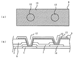
さらに、下地金属層13が設けられている部分の面積を広げることにより、ゲート端子、ゲート配線、ソース端子やソース配線等の抵抗を下げることが可能である。端子や配線の抵抗を下げるための構成について図2を用いて説明する。図2は第1の金属配線と第2の金属配線を電気的に接続するためのコンタクトホールが設けられている部分の構成を示す図である。図2(a)は平面図であり、図2(b)は断面図である。図1で付した符号と同一の符号は同一の構成を示すため説明を省略する。14は第2の金属薄膜である。
第1の金属薄膜1と第2の金属薄膜14は表示領域以外の領域等で接続されることがある。例えば、外部の駆動回路と接続可能な場所に端子を配置するためには、第1の金属薄膜で形成され、かつ異なる信号が印加される配線同士あるいは第2の金属薄膜で形成され、かつ異なる信号が印加される配線同士をクロスさせる必要がある。あるいは、携帯電話などに用いられるCOG基板等の端子部近傍においても、配線をクロスさせる必要がある。このように同じ配線をクロスさせるためには、どちらか一方の金属配線を他の金属配線に変換する必要がある。このため、第1の金属配線1と第2の金属配線14を接続させる必要がある。以下にその詳細を説明する。
【0053】
図2の構成の各層は上述の製造方法と同様の製造方法によって形成されている。図2(a)に示すように、有機膜8上で下地金属薄膜13のパターンは導電性薄膜9のパターンと略同程度の大きさとしている。このように第1の金属薄膜1と第2の金属薄膜14を電気的に接続させる場合、従来は導電性薄膜9によって接続させていたが、本実施の形態では比抵抗の良いクロム等の金属薄膜で接続させている。このため、2つ以上のコンタクトホール間の抵抗を小さくできるため、配線や端子の抵抗を下げることができる。さらに、導電性薄膜9と第1の金属薄膜1又は第2の金属薄膜14が下地金属薄膜13を介して電気的に接続されているため、コンタクト抵抗の劣化が抑制される。このように下地金属薄膜13のパターンと導電性薄膜9のパターンの形状を略同じ大きさとすることにより、配線や端子の抵抗を下げることが可能になる。下地金属薄膜13による接続は第1の金属薄膜1同士を電気的に接続させる場合や、第2の金属薄膜14同士を電気的に接続させる場合であっても利用することが可能である。なお、第3の金属薄膜10、11のエッチングによって、下地金属薄膜13がエッチングされない場合は、下地金属薄膜13の上の導電性薄膜9を形成しなくても良い。
【0054】
このように下地金属薄膜13のパターンと導電性薄膜9のパターンの形状を略同じ大きさとすることは、第5のフォトリソグラフィー工程によって可能である。よって、フォトリソグラフィー工程を増やすことなく、簡易な製造工程で製造することが可能である。もちろん、全ての箇所において下地金属薄膜13のパターンと導電性薄膜9のパターンの形状を略同じ大きさとする必要はなく、例えば、TFT部や反射部を除いた必要な箇所のみ略同じ大きさとすればよい。
【0055】
なお、下地金属薄膜13と第3の金属薄膜10、11が同じエッチング工程によりエッチングできる場合は第7のフォトリソグラフィー工程で下地金属薄膜13を導電性薄膜9と略同じパターン形状にすることも可能である。例えば下地金属薄膜13と第3の金属薄膜10が同じ材質である場合、第3の金属薄膜10をエッチングする工程において、導電性薄膜9からはみ出している部分の下地金属膜13はエッチングされる。すなわち、第5のフォトリソグラフィー工程で下地金属薄膜13のパターンを導電性薄膜9のパターンより大きく形成しても、第7のフォトリソグラフィー工程のエッチング工程で下地金属薄膜13はエッチングされ、導電性薄膜9と略同じ大きさとなる。このように第7のフォトリソグラフィー工程でも下地金属薄膜13をパターニングすることができる。
【0056】
本実施の形態では、下地金属薄膜13を介して第1の金属薄膜1又は第2の金属薄膜と導電性薄膜9が電気的に接続されているので、コンタクト抵抗を低減することができる。さらに、下地金属薄膜13の面積を広げることにより、電極、端子、配線の抵抗を低減することが可能になる。このように簡易な製造方法及び簡易な構成により、抵抗が低減された液晶表示装置を得ることができ、表示品質、生産性を向上することができる。
【0057】
発明の実施の形態2.
上述の実施の形態1では抵抗を低減するため図2に示すように、導電性薄膜9のパターンと下地金属薄膜13のパターンを略同程度の大きさとしている。しかし、下地金属薄膜13、第3の金属薄膜10、11、有機膜8及び導電性薄膜9の材料、膜質によっては、第7のフォトリソグラフィー工程のエッチング工程で下地金属薄膜13が溶けてしまう場合があることを本件の出願人は発見した。導電性薄膜9の下に設けられた下地金属薄膜13が溶け出してしまうと、導電性薄膜9と有機膜8との間に隙間が生じる。図2で示した構成の場合、導電性薄膜9の下に設けられている下地金属薄膜13の面積と導電性薄膜9の面積の差がコンタクトホール12の分しかないため、導電性薄膜9のほとんどの部分でこの隙間が生じる。そのため導電性薄膜9とその下地層との密着力の低下が生じ、膜剥がれが発生してしまう。
【0058】
このように導電性薄膜9と略同程度の大きさで形成された下地金属薄膜13が溶けてしまうと密着力が低下して、その上の導電性薄膜9の膜剥がれが生じるおそれがある。しかし、本件の出願人はこの膜剥がれは下地金属薄膜13の下が有機膜8である場合に発生する可能性が高いことを発見した。この知見より膜剥がれを効果的に抑制する構成を見出した。この膜剥がれを防ぐための構成について図3を用いて説明する。
【0059】
図3は第1の金属配線1と第2の金属配線14を電気的に接続するためのコンタクトホールが設けられている部分の構成を示す図であり、図2と同様の図である。図3(a)は平面図であり、図3(b)は断面図である。図1、図2で付した符号と同一の符号は同一の構成を示すため説明を省略する。また製造方法も実施の形態1で説明した方法と同じであるため説明を省略する。
【0060】
本実施の形態では、膜剥がれを回避するために下地金属薄膜13がコンタクトホール12の上部と略同じ大きさで設けられている。よって、有機膜8の上には下地金属薄膜13を介さずにITO等の導電性薄膜9が直接成膜されることになる。そのため、第3の金属薄膜10のエッチング工程において、導電性薄膜9の大部分はエッチング液による影響を受けない。またコンタクトホール12の上に設けられた下地金属薄膜13は下地が有機層7でないため、溶け出しにくい。また溶け出したとしても、導電性薄膜9のパターンに占める割合が小さいので密着力の低下を抑制することができる。従って、ITO等の導電性薄膜9の膜剥がれを防ぐことができる。
【0061】
なお、コンタクトホール12と略同じ大きさの下地金属薄膜13を形成するためには、第5のフォトリソグラフィー工程でコンタクトホール12と略同じ大きさで露光する。ただし、露光時の位置ずれやエッチング形状などを考慮する必要がある。すなわち、露光時の基板の位置ずれや下地金属薄膜13のエッチング形状等によって露光した領域と実際のパターン形状がずれる場合がある。コンタクトホール12と全く同じ大きさで露光してしまった場合、ずれが生じるとコンタクトホール12及びその下の第1の金属薄膜1又は第2の金属薄膜14が露出してしまい、エッチング液に第1の金属薄膜等が溶け出すおそれがある。
【0062】
本実施の形態では、コンタクトホール12より5μm程度大きい領域を下地金属薄膜13のパターンが覆うように設計上露光することにしている。この5μmは設計上の露光領域と実際のパターン形状とのプロセス上の最大ずれ量である。プロセスマージンで許される最小値5μm分だけコンタクトホール12より大きい領域を設計上の下地金属薄膜13のパターン領域とすることによって、プロセス上のずれが生じた場合であっても、コンタクトホール12を全て覆うように下地金属薄膜13を形成することが可能である。
このようにして、コンタクトホール12と下地金属薄膜13を略同じ大きさでかつ、コンタクトホール12が下地金属薄膜13で覆われるように形成することができる。これにより密着力の低下を抑制することができ、ITO等の導電性薄膜の膜剥がれを防ぐことができる。なお、膜剥がれを防ぐためには下地金属薄膜13はコンタクトホール12を覆うように形成し、かつ下地金属薄膜13の大きさを出来る限り小さくすることが望ましい。設計上の露光領域の大きさは上述の値に限られるものではない。膜剥がれが生じないような膜質、材料を用いている場合は、配線や端子の抵抗の点から図2で示したように導電性薄膜9と下地金属薄膜13の大きさを略同じ大きさとすることが望ましい。
【0063】
その他の実施の形態.
本発明は上述した実施の形態だけに限られず、様々な変更が可能である。例えば、上述の実施の形態において、第1の金属薄膜1、第2の金属薄膜、下地金属薄膜13にはクロムを用いたが、それ以外の材料でもよい。さらには、有機膜8、第1の絶縁膜2、第2の絶縁膜7及び導電性薄膜9も同様に公知の材料を用いることができる。第1の金属薄膜1、第2の金属薄膜、下地金属薄膜13を異なる材料で形成してもよい。さらには、実施の形態で示した膜厚などの数値は例であり、これ以外の値で製造することも可能である。本発明は携帯電話、PDA、車載用の半透過型液晶表示装置に用いることが好適である。また、半透過型液晶表示装置に限らず、透過型液晶表示装置や反射型液晶表示装置に用いることも可能である。
【0064】
【発明の効果】
本発明によれば、配線等の抵抗が低減された液晶表示装置及びその製造方法を提供することができる。
【図面の簡単な説明】
【図1】 本発明の実施の形態1にかかる液晶表示装置の製造方法を示す断面図である。
【図2】 本発明の実施の形態1にかかる液晶表示装置の端子部の構成を示す構成図である。
【図3】 本発明の実施の形態2にかかる液晶表示装置の端子部の構成を示す構成図である。
【図4】 従来の液晶表示装置の製造方法を示す断面図である。
【符号の説明】
1 第1の金属薄膜 2 第1の絶縁膜
3 半導体能動膜 4 オーミックコンタクト膜
5 ソース電極 6 ドレイン電極
7 第2の絶縁膜 8 有機膜
9 導電性薄膜 10,11 第3の金属薄膜
12 コンタクトホール、13 下地金属薄膜、
14 第2の金属薄膜、15 凹部[0001]
BACKGROUND OF THE INVENTION
The present invention relates to a liquid crystal display device and a manufacturing method thereof.
[0002]
[Prior art]
In general, in a liquid crystal display device, a liquid crystal layer made of liquid crystal is sandwiched between two substrates each having an electrode on the upper surface and the lower surface, and polarizing plates are installed on the upper and lower sides of the two substrates. The thing has the structure where the backlight was installed in the back. Surfaces having electrodes on these substrates are subjected to a so-called alignment treatment, and a director that shows the orientation of liquid crystal molecules on average is birefringent in the desired liquid crystal, and light incident from the backlight through the polarizing plate. Changes to elliptically polarized light due to birefringence and is incident on the polarizing plate on the opposite side. In this state, when a voltage is applied between the upper and lower electrodes, the alignment state of the director is changed, the birefringence of the liquid crystal layer is changed, and the elliptical polarization state incident on the opposite polarizing plate is changed. An electro-optic effect that changes the intensity and spectrum of light transmitted through the liquid crystal display device can be obtained.
[0003]
In the liquid crystal display device, a backlight (back light source) is installed on the back or side, and a transmissive liquid crystal display device that displays images and a reflector on the substrate, and ambient light is reflected on the reflector surface. There is a reflective liquid crystal display device that displays an image by performing the above operation. This transmissive liquid crystal display device has a problem in that when the ambient light is very bright, the display cannot be observed because the display light is darker than the ambient light. On the other hand, the reflective liquid crystal display device has a drawback that the visibility is extremely lowered when the ambient light is dark.
[0004]
In order to solve these problems, a liquid crystal display device using a transflective film that transmits part of light and reflects part of light (hereinafter referred to as a transflective liquid crystal display device) has been proposed. (For example, Patent Document 1, Patent Document 2, and Patent Document 3). The applicant of the present application has also developed a transflective liquid crystal display device (for example, Patent Document 4).
[0005]
A method of manufacturing the transflective liquid crystal display device will be described with reference to FIG. FIG. 4 is a cross-sectional view showing an example of a manufacturing process of a TFT substrate used in a conventional liquid crystal display device. 1 is a first metal thin film, 2 is a first insulating film, 3 is a semiconductor active film, 4 is an ohmic contact film, 5 is a source electrode, 6 is a drain electrode, 7 is a second insulating film, and 8 is an organic film , 9 are conductive thin films.
[0006]
First, the first metal thin film 1 is formed on a glass substrate by sputtering or the like. A gate wiring, a gate electrode, and a gate terminal are formed by a first photolithography process. As the first metal thin film, chromium, molybdenum, tantalum, titanium, aluminum, copper, an alloy obtained by adding a small amount of other substances to these, or a laminated film thereof is used. The structure shown in FIG. 4A is formed by the process described above.
[0007]
Next, the first insulating film 2, the semiconductor active film 3, and the ohmic contact film 4 are continuously formed by plasma CVD. The first insulating film 2 is made of, for example, SiNx or SiOy, and is used as a gate insulating film. As the semiconductor active film 3, an amorphous silicon (a-Si) film or a polysilicon (p-Si) film is used. As the ohmic contact film 4, an na-Si film or an np-Si film obtained by doping a-Si or p-Si with a small amount of phosphorus (P) or the like is used. Next, the semiconductor active film 3 and the ohmic contact film 4 are patterned at least in a portion where the TFT portion is formed by a second photolithography process. Thereby, the structure shown in FIG. 4B is formed.
[0008]
A second metal thin film is formed by a method such as sputtering. As the second metal thin film, for example, chromium, molybdenum, tantalum, titanium, aluminum, copper, an alloy obtained by adding a small amount of other substances to these, or a laminated film thereof is used. Next, patterning is performed so that the second metal thin film forms the source electrode 5 and the drain electrode 6 in a third photolithography process. Next, the ohmic contact film 4 is etched. By this process, the central portion of the ohmic contact film 4 in the TFT portion is removed, and the semiconductor active film 3 is exposed. Thereby, the structure shown in FIG. 4C is formed.
[0009]
Further, after the second insulating film 7 and the
[0010]
Further, a conductive
[0011]
However, the liquid crystal display device formed by such a process has the following problems. In the above-described configuration, the conductive
[0012]
[Patent Document 1]
JP 7-333598 A
[Patent Document 2]
JP 2000-19563 A
[Patent Document 3]
JP 2000-305110 A
[Patent Document 4]
Japanese Patent Application No. 2002-048074
[0013]
[Problems to be solved by the invention]
As described above, the conventional liquid crystal display device has a problem in that the resistance of the wiring, terminal, or electrode deteriorates and the display characteristics and display quality deteriorate.
[0014]
The present invention has been made in order to solve such problems, and provides a liquid crystal display device having good display characteristics and display quality, and a manufacturing method thereof, which prevents deterioration of the resistance of wiring, terminals or electrodes. For the purpose.
[0015]
[Means for Solving the Problems]
A liquid crystal display device according to the present invention is a liquid crystal display device including a pair of substrates disposed to face each other with a liquid crystal layer interposed therebetween, and is a first one provided on one of the pair of substrates. Conductive film (for example, the first metal thin film 1 or the second metal thin film in the embodiment of the present invention) and an insulating film provided on the first conductive film (for example, implementation of the present invention) The first insulating film 2 or the second insulating film 7 in the embodiment and a contact hole provided by removing a part of the insulating film (for example, the first insulating
[0016]
In the above liquid crystal display device, a reflective or transflective display device can be realized by further including a reflective electrode provided on the transparent conductive film.
[0017]
It is desirable that the reflective electrode and the second conductive film have substantially the same size. Thereby, peeling of the transparent conductive film at the time of etching of the reflective electrode can be prevented.
[0018]
The liquid crystal display device according to the present invention further includes an organic layer formed under the second conductive film in the liquid crystal display device described above, and the contact hole includes a part of the insulating film and a part of the organic film. It is formed by removing.
[0019]
The liquid crystal display device according to the present invention is characterized in that, in the above-described liquid crystal display device, the second conductive film is substantially the same size as the contact hole. Thereby, film peeling of the conductive thin film can be prevented.
In a preferred embodiment of the above-described liquid crystal display device, the pattern of the second conductive film includes the pattern of the contact hole, and the overlap amount is 5 μm or less on one side.
[0020]
The liquid crystal display device according to the present invention is characterized in that, in the above-described liquid crystal display device, the second conductive film is substantially the same size as the transparent conductive film. As a result, the resistance when two or more contact holes are connected by a single transparent conductive film can be reduced.
[0021]
6. The liquid crystal display device according to claim 5, wherein the second conductive film is approximately the same size as the transparent conductive film at a location where two or more contact holes are connected by the transparent conductive film.
[0022]
A manufacturing method of a liquid crystal display device according to the present invention is a manufacturing method of a liquid crystal display device including a pair of substrates disposed to face each other with a liquid crystal layer interposed therebetween, on one of the pair of substrates. Forming a first conductive film, forming an insulating film on the first conductive film, removing a portion of the insulating film to form a contact hole, and the contact hole Forming a second conductive film so as to cover the surface, and providing a transparent conductive film electrically connected to the second conductive film. Thereby, contact resistance can be reduced.
[0023]
In the manufacturing method described above, a reflective or transflective display device can be realized by further including a step of forming a reflective electrode on the transparent conductive film.
[0024]
In the manufacturing method described above, in the step of forming the reflective electrode, it is desirable that the reflective electrode is patterned with approximately the same size as the second conductive film. Thereby, peeling of the transparent conductive film during etching of the reflective electrode can be prevented.
[0025]
The liquid crystal display device according to the present invention further includes a step of forming an organic layer on the insulating film in the manufacturing method described above, and in the step of forming the contact hole, the insulating film and a part of the organic film are removed. Thus, a contact hole is formed.
[0026]
In a preferred embodiment of the above manufacturing method, in the step of forming the contact hole, a part of the insulating film or a part of the contact hole is removed by dry etching.
[0027]
In the step of forming the second conductive film in the manufacturing method described above, it is desirable that the second conductive film be patterned to have approximately the same size as the contact hole. Thereby, film peeling of a transparent conductive film can be prevented.
[0028]
In the step of forming the second conductive film of the above-described manufacturing method, the second conductive film may be patterned with substantially the same size as the transparent conductive film. Thereby, resistance of wiring etc. can be reduced.
[0029]
In the step of forming the second conductive film of the manufacturing method described above, the second conductive film is substantially the same as the transparent conductive film at a location where two or more contact holes are connected by the transparent conductive film. You may pattern by a magnitude | size. Thereby, the resistance of the terminal that performs input / output with the outside can be reduced.
[0030]
DETAILED DESCRIPTION OF THE INVENTION
Embodiment 1 of the Invention
FIG. 1 shows a manufacturing process flow of a transflective liquid crystal display device according to Embodiment 1 of the present invention. In this manufacturing process, a transflective a-Si TFT array is manufactured by seven photographic processes. 1 is a first metal thin film, 2 is a first insulating film, 3 is a semiconductor active film, 4 is an ohmic contact film, 5 is a source electrode, 6 is a drain electrode, 7 is a second insulating film, and 8 is an organic film , 9 are conductive thin films, 10 and 11 are third metal thin films, 12 are contact holes, 13 is a base metal thin film, and 15 is a recess. The pattern shape shown in FIG. 1 shows a gate terminal portion, a source terminal portion, a crossing portion of the source wiring and the gate wiring, a TFT portion, a reflection portion of the display region, and a transmission portion of the display region in order from the left. The gate terminal portion and the source terminal portion are provided, for example, in a region other than the display region at the substrate end portion, and a signal is input from the drive circuit through these terminals. The TFT portion is provided corresponding to each pixel in the display area. The intersection between the source wiring and the gate wiring is provided in the vicinity of the TFT portion. The reflection part is provided with a reflection electrode in each pixel, and the transmission part is provided with a transmission electrode in each pixel. The reflective electrode and the transmissive electrode constitute a pixel electrode of each pixel.
[0031]
First, a glass substrate is cleaned as an insulating substrate to clean the surface. As the insulating substrate, a transparent insulating substrate such as a glass substrate is used. The thickness of the insulating substrate may be arbitrary, but it is preferably 1.1 mm or less in order to reduce the thickness of the liquid crystal display device. If the insulating substrate is too thin, the substrate may be distorted due to various film formation and thermal history of the process, resulting in problems such as reduced patterning accuracy. Therefore, the thickness of the insulating substrate takes into account the process used. Need to choose. Further, when the insulating substrate is made of a brittle fracture material such as glass, it is preferable to chamfer the end surface of the substrate in order to prevent foreign matters from being mixed due to chipping from the end surface. In addition, it is preferable to provide a notch in a part of the insulating substrate so that the orientation of the substrate can be specified, because the direction of substrate processing in each process can be specified, thereby facilitating process management.
[0032]
Next, the first metal thin film 1 is formed by a method such as sputtering. As the first metal thin film 1, for example, a thin film having a thickness of about 100 nm to 500 nm made of any one of chromium, molybdenum, tantalum, titanium, aluminum, copper, and an alloy obtained by adding a trace amount of other substances to these is used. be able to. In the preferred embodiment, 200 nm thick chromium is used. A contact hole is formed on the first metal thin film 1 by dry etching in a process to be described later, and a conductive thin film is formed on the contact hole. The metal thin film is preferably used for the first metal thin film 1, and at least the surface is preferably made of chromium, titanium, tantalum, molybdenum, or the like. Further, as the first metal thin film 1, a metal thin film in which different kinds of metal thin films are laminated or a metal thin film having a different composition in the film thickness direction can also be used. Further, when a material containing aluminum is used as the first metal thin film 1, it is preferable that at least the surface is aluminum nitride having a specific resistance of about 10 to 1000 μΩ.
[0033]
Next, the first metal thin film 1 is patterned by a first photolithography process (photographic process) to form a gate electrode and a gate wiring, an auxiliary capacitance electrode and an auxiliary capacitance wiring, a gate terminal, and the like. Thereby, the structure shown in FIG. 1A is formed. In the photolithography process, after the TFT array substrate is washed, a photosensitive resist is applied and dried, then exposed through a mask pattern in which a predetermined pattern is formed, and developed to make a mask pattern on the TFT array substrate photolithography. This is performed by forming a resist to which the resist is transferred, heating and curing the photosensitive resist, etching, and peeling the photosensitive resist. If the wettability between the photosensitive resist and TFT array substrate is poor and the photosensitive resist repels, UV cleaning is performed before coating, or HMDS (hexamethyldisilazane) is used to improve wettability. Processes such as applying steam. Further, when the adhesion between the photosensitive resist and the TFT array substrate is poor and peeling occurs, the heat curing temperature is increased or the time is increased. Etching of the first metal thin film 1 is performed by wet etching using a known etchant (for example, when the first metal thin film 1 is made of chromium, an aqueous solution in which second ceric ammonium nitrate and nitric acid are mixed). It can be etched. The first metal thin film 1 is preferably etched so that the pattern edge has a tapered shape, in order to prevent a short circuit at a step with another wiring. Here, the taper shape means that the pattern edge is etched so that the cross section has a trapezoidal shape. In addition, although it has been shown that the gate electrode and the gate wiring, the auxiliary capacitance electrode and the auxiliary capacitance wiring are formed in this step, various other marks and wirings necessary for manufacturing the TFT array substrate are formed.
[0034]
Next, the first insulating film 2, the semiconductor active film 3, and the ohmic contact film 4 are continuously formed by plasma CVD. As the first insulating film 2 serving as a gate insulating film, a SiNx film, a SiOy film, a SiOzNw film, or a laminated film thereof is used (x, y, z, and w are positive numbers). The film thickness of the first insulating film 2 is about 300 nm to 600 nm. When the film thickness is small, a short circuit is likely to occur at the intersection of the gate wiring and the source wiring, and it is preferable that the thickness be about the thickness of the first metal thin film 1. When the film thickness is large, the ON current of the TFT becomes small and the display characteristics are deteriorated. In a preferred embodiment, a first insulating film 2 is formed by forming a 300 nm SiN film and then forming a 100 nm SiN film.
[0035]
As the semiconductor active film 3, an amorphous silicon (a-Si) film or a polysilicon (p-Si) film is used. The film thickness of the semiconductor active film 3 is about 100 nm to 300 nm. When the film thickness is thin, the ohmic contact film 4 to be described later disappears during dry etching. When the film thickness is thick, the ON current of the TFT is reduced, so that the etching depth of the ohmic contact film 4 during dry etching is reduced. The film thickness is selected based on the controllability and the required ON current of the TFT. When an a-Si film is used as the semiconductor active film 3, the interface between the first insulating film 2 and the a-Si film is a SiNx film or a SiOzNw film. It is preferable in terms of controllability and reliability of Vth. When a p-Si film is used as the semiconductor active film 3, it is preferable that the interface between the first insulating film 2 and the p-Si film is a SiOy film or a SiOzNw film in terms of controllability and reliability of Vth of the TFT. When an a-Si film is used as the semiconductor active film 3, the vicinity of the interface with the first insulating film 2 is formed under a condition with a low film formation rate, and the upper layer is formed under a condition with a high film formation rate. It is more preferable that TFT characteristics with high mobility can be obtained in a short film formation time and that the leakage current when the TFT is turned off can be reduced. In a preferred embodiment, a 150 nm a-Si film is formed as the semiconductor active film 3.
[0036]
As the ohmic contact film 4, an na-Si film or an np-Si film obtained by doping a-Si with a small amount of phosphorus (P) is used. The thickness of the ohmic contact film 4 can be about 20 nm to 70 nm. These SiNx film, SiOy film, SiOzNw film, a-Si film, p-Si film, na-Si film, and np-Si film are formed of a known gas (SiH 4 , NH Three , H 2 , NO 2 , PH 3 , N 2 And a mixed gas thereof). In a preferred embodiment, a 30 nm na-Si film is deposited as the ohmic contact film 4.
[0037]
Next, the semiconductor active film 3 and the ohmic contact film 4 are patterned at least in a portion where the TFT portion is formed by a second photolithography process. As a result, the structure shown in FIG. 1B is formed. The first insulating film 2 remains throughout. The semiconductor active film 3 and the ohmic contact film 4 can be left by patterning and remaining in a portion where the source wiring, the gate wiring, and the auxiliary capacitance wiring cross in a plane in addition to the portion where the TFT portion is formed. It is more preferable that the withstand voltage becomes larger. Further, the semiconductor active film 3 and the ohmic contact film 4 in the TFT portion remain in a continuous shape up to the lower portion of the source wiring, so that the source electrode does not get over the step between the semiconductor active film 3 and the ohmic contact film 4 and the step portion This is preferable because disconnection of the source electrode is difficult to occur.
[0038]
Etching of the semiconductor active film 3 and the ohmic contact film 4 is performed by a known gas composition (for example, SF 6 And O 2 Mixed gas or CF Four And O 2 Can be dry-etched with a mixed gas).
[0039]
Next, a second metal thin film is formed by a method such as sputtering. As the second metal thin film, for example, chromium, molybdenum, tantalum, titanium, aluminum, copper, an alloy obtained by adding a small amount of other substances to these, or a laminated film thereof is used. Of course, the above-described materials may be laminated. In a preferred embodiment, chromium having a thickness of 200 nm is deposited.
[0040]
Next, patterning is performed so that the second metal thin film forms the source wiring, the source terminal, the source electrode 5 and the drain electrode 6 by a third photolithography process. Thereby, the structure shown in FIG. 1C is formed. The source electrode 5 is formed over a portion where the source wiring and the gate wiring intersect. The drain electrode 6 is formed over the reflection portion. Next, the ohmic contact film 4 is etched. By this process, the central portion of the ohmic contact film 4 in the TFT portion is removed, and the semiconductor active film 3 is exposed. The ohmic contact film 4 is etched by a known gas composition (for example, SF 6 And O 2 Mixed gas or CF Four And O 2 Can be dry-etched with a mixed gas).
[0041]
Next, the second insulating film 7 is formed by plasma CVD. An
[0042]
Next, the
[0043]
In the gate terminal portion, both the
[0044]
Thereafter, in the present invention, the base metal
[0045]
Next, the conductive
[0046]
Next, the conductive
[0047]
Next, the metal
[0048]
Next, in the seventh photolithography process, the third metal
[0049]
An alignment film is applied from above, and a TFT array substrate is manufactured by rubbing in a certain direction. The TFT array substrate manufactured in this way is bonded to the CF substrate arranged opposite to each other via a spacer, and liquid crystal is injected therebetween. A liquid crystal display device is manufactured by attaching the liquid crystal panel sandwiched between the liquid crystal layers to the backlight unit.
[0050]
In this embodiment, a part of the
[0051]
In general, the specific resistance of a metal thin film such as chromium is better than that of a transparent conductive film such as ITO. Therefore, by increasing the area of the portion where the base metal
In the conventional liquid crystal display device, when the
[0052]
Furthermore, by increasing the area of the portion where the
The first metal thin film 1 and the second metal
[0053]
Each layer of the configuration of FIG. 2 is formed by a manufacturing method similar to the above-described manufacturing method. As shown in FIG. 2A, the pattern of the base metal
[0054]
Thus, it is possible to make the pattern of the base metal
[0055]
If the base metal
[0056]
In the present embodiment, since the first metal thin film 1 or the second metal thin film and the conductive
[0057]
Embodiment 2 of the Invention
In the first embodiment described above, in order to reduce the resistance, the pattern of the conductive
[0058]
As described above, when the underlying metal
[0059]
FIG. 3 is a diagram showing a configuration of a portion provided with a contact hole for electrically connecting the first metal wiring 1 and the
[0060]
In the present embodiment, the base metal
[0061]
In order to form the base metal
[0062]
In the present embodiment, the design exposure is performed so that the pattern of the base metal
In this way, the
[0063]
Other embodiments.
The present invention is not limited to the above-described embodiment, and various modifications can be made. For example, in the above-described embodiment, chromium is used for the first metal thin film 1, the second metal thin film, and the base metal
[0064]
【The invention's effect】
ADVANTAGE OF THE INVENTION According to this invention, the liquid crystal display device with which resistance, such as wiring, was reduced, and its manufacturing method can be provided.
[Brief description of the drawings]
FIG. 1 is a cross-sectional view illustrating a method for manufacturing a liquid crystal display device according to a first embodiment of the present invention.
FIG. 2 is a configuration diagram showing a configuration of a terminal portion of the liquid crystal display device according to the first exemplary embodiment of the present invention;
FIG. 3 shows an embodiment of the present invention. 2 It is a block diagram which shows the structure of the terminal part of the liquid crystal display device concerning.
FIG. 4 is a cross-sectional view illustrating a conventional method for manufacturing a liquid crystal display device.
[Explanation of symbols]
DESCRIPTION OF SYMBOLS 1 1st metal thin film 2 1st insulating film
3 Semiconductor active film 4 Ohmic contact film
5 Source electrode 6 Drain electrode
7 Second insulating
9 Conductive
12 contact holes, 13 underlying metal thin film,
14 Second metal thin film, 15 recess
Claims (12)
前記一対の基板のうちの一方の基板上に設けられた第1の導電膜と、
前記第1の導電膜の上に設けられた絶縁膜と、
前記絶縁膜の一部を除去することにより設けられたコンタクトホールと、
前記コンタクトホールを覆うように設けられ、前記第1の導電膜と電気的に接続された第2の導電膜と、
前記第2の導電膜上に設けられ、前記第2の導電膜と電気的に接続された透明導電膜と
前記透明導電膜の上に設けられた反射電極と、を備え、
前記表示領域において前記第2の導電膜の大きさが前記反射電極と略同じであることを特徴とする液晶表示装置。A liquid crystal display device comprising a pair of substrates disposed opposite to each other with a liquid crystal layer interposed therebetween, wherein pixels are provided in a display region,
A first conductive film provided on one of the pair of substrates;
An insulating film provided on the first conductive film;
A contact hole provided by removing a part of the insulating film;
A second conductive film provided to cover the contact hole and electrically connected to the first conductive film;
A transparent conductive film provided on the second conductive film and electrically connected to the second conductive film; and a reflective electrode provided on the transparent conductive film,
The liquid crystal display device, wherein the size of the second conductive film in the display region is substantially the same as that of the reflective electrode.
前記コンタクトホールが前記絶縁膜の一部及び前記有機膜の一部を除去することにより形成されることを特徴とする請求項1に記載の液晶表示装置。An organic layer formed under the second conductive film;
The liquid crystal display device according to claim 1, wherein the contact hole is formed by removing a part of the insulating film and a part of the organic film.
前記一対の基板のうちの一方の基板上に第1の導電膜を形成するステップと、
前記第1の導電膜の上に絶縁膜を形成するステップと、
前記絶縁膜の一部を除去してコンタクトホールを形成するステップと、
前記コンタクトホールを覆うように第2の導電膜を形成するステップと、
前記第2の導電膜上に、前記第2の導電膜と電気的に接続された透明導電膜を設けるステップと、
前記透明導電膜の上に反射電極を形成するステップと、を備え、
前記表示領域において、前記第2の導電膜の大きさが前記反射電極と略同じであることを特徴とする液晶表示装置の製造方法。A method for manufacturing a liquid crystal display device, comprising a pair of substrates disposed opposite to each other with a liquid crystal layer interposed therebetween, wherein pixels are provided in a display region,
Forming a first conductive film on one of the pair of substrates;
Forming an insulating film on the first conductive film;
Removing a part of the insulating film to form a contact hole;
Forming a second conductive film so as to cover the contact hole;
Providing a transparent conductive film electrically connected to the second conductive film on the second conductive film;
Forming a reflective electrode on the transparent conductive film,
In the display region, the size of the second conductive film is substantially the same as that of the reflective electrode.
前記コンタクトホールを形成するステップでは、前記絶縁膜及び前記有機膜の一部を除去することによりコンタクトホールを形成することを特徴とする請求項7に記載の液晶表示装置の製造方法。Forming an organic layer on the insulating film;
8. The method of manufacturing a liquid crystal display device according to claim 7, wherein in the step of forming the contact hole, the contact hole is formed by removing a part of the insulating film and the organic film.
Priority Applications (1)
| Application Number | Priority Date | Filing Date | Title |
|---|---|---|---|
| JP2003087625A JP4354205B2 (en) | 2003-03-27 | 2003-03-27 | Liquid crystal display device and manufacturing method thereof |
Applications Claiming Priority (1)
| Application Number | Priority Date | Filing Date | Title |
|---|---|---|---|
| JP2003087625A JP4354205B2 (en) | 2003-03-27 | 2003-03-27 | Liquid crystal display device and manufacturing method thereof |
Publications (2)
| Publication Number | Publication Date |
|---|---|
| JP2004294807A JP2004294807A (en) | 2004-10-21 |
| JP4354205B2 true JP4354205B2 (en) | 2009-10-28 |
Family
ID=33401972
Family Applications (1)
| Application Number | Title | Priority Date | Filing Date |
|---|---|---|---|
| JP2003087625A Expired - Fee Related JP4354205B2 (en) | 2003-03-27 | 2003-03-27 | Liquid crystal display device and manufacturing method thereof |
Country Status (1)
| Country | Link |
|---|---|
| JP (1) | JP4354205B2 (en) |
Cited By (1)
| Publication number | Priority date | Publication date | Assignee | Title |
|---|---|---|---|---|
| CN105487285A (en) * | 2016-02-01 | 2016-04-13 | 深圳市华星光电技术有限公司 | Array substrate and preparing method of array substrate |
Families Citing this family (6)
| Publication number | Priority date | Publication date | Assignee | Title |
|---|---|---|---|---|
| KR101139522B1 (en) * | 2004-12-04 | 2012-05-07 | 엘지디스플레이 주식회사 | Thin Film Transistor Substrate of Transflective Type And Method for Fabricating The Same |
| KR101237115B1 (en) | 2005-12-26 | 2013-02-25 | 엘지디스플레이 주식회사 | Backlight Device with Light Emitting Diodes and Fabricating Method thereof |
| JP5011479B2 (en) * | 2006-02-14 | 2012-08-29 | 株式会社ジャパンディスプレイイースト | Manufacturing method of display device |
| CN100412632C (en) * | 2006-06-30 | 2008-08-20 | 友达光电股份有限公司 | Manufacturing method of array substrate of semi-reflection semi-penetration liquid crystal display |
| JP5477612B2 (en) * | 2008-04-17 | 2014-04-23 | 株式会社ジャパンディスプレイ | Display device and electronic device |
| JP5339273B2 (en) * | 2008-07-11 | 2013-11-13 | 株式会社ジャパンディスプレイ | Display device |
-
2003
- 2003-03-27 JP JP2003087625A patent/JP4354205B2/en not_active Expired - Fee Related
Cited By (3)
| Publication number | Priority date | Publication date | Assignee | Title |
|---|---|---|---|---|
| CN105487285A (en) * | 2016-02-01 | 2016-04-13 | 深圳市华星光电技术有限公司 | Array substrate and preparing method of array substrate |
| US10048556B2 (en) | 2016-02-01 | 2018-08-14 | Shenzhen China Star Optoelectronics Technology Co., Ltd | Array substrate having multiple common electrode lines |
| CN105487285B (en) * | 2016-02-01 | 2018-09-14 | 深圳市华星光电技术有限公司 | The preparation method of array substrate and array substrate |
Also Published As
| Publication number | Publication date |
|---|---|
| JP2004294807A (en) | 2004-10-21 |
Similar Documents
| Publication | Publication Date | Title |
|---|---|---|
| JP3977099B2 (en) | Liquid crystal display device and manufacturing method thereof | |
| KR101398643B1 (en) | Thin film transistor substrate, method for manufacturing the same and liquid crystal display panel having the same | |
| US7833813B2 (en) | Thin film transistor array panel and method of manufacturing the same | |
| US20020044228A1 (en) | Array substrate for a liquid crystal display and method for fabricating thereof | |
| US6184960B1 (en) | Method of making a reflective type LCD including providing a protective metal film over a connecting electrode during at least one portion of the manufacturing process | |
| JPH11281992A (en) | Liquid crystal display and its production | |
| JP4472990B2 (en) | Reflective liquid crystal display device and manufacturing method thereof | |
| US20090091699A1 (en) | Liquid crystal display device and fabricating method thereof | |
| JP5007171B2 (en) | Thin film transistor array substrate, manufacturing method thereof, and display device | |
| KR100802457B1 (en) | Liquid crystal display apparatus and manufacturing method thereof | |
| US7630049B2 (en) | Display device and method with lower layer film formed on substrate but between transparent conductive film and organic layer and then protective film on the transparent film | |
| US20070085116A1 (en) | Array substrate for liquid crystal display device and manufacturing method of the same | |
| JP3513409B2 (en) | Liquid crystal display device and method of manufacturing the same | |
| US20070188682A1 (en) | Method for manufacturing a display device | |
| JP2005338388A (en) | Liquid crystal display and its manufacturing method | |
| JP4354205B2 (en) | Liquid crystal display device and manufacturing method thereof | |
| JP2004294805A (en) | Liquid crystal display, manufacturing method of display device, and patterning method | |
| US20070097282A1 (en) | Thin film multilayer substrate, manufacturing method thereof, and liquid crystal display having thin film multilayer substrate | |
| JP4237679B2 (en) | Display device and manufacturing method thereof | |
| KR100827856B1 (en) | Array substrate of transflective type fringe field switching mode liquid crystal display and the method thereof | |
| JPH1195248A (en) | Array substrate for display device and its production | |
| JP4227055B2 (en) | Manufacturing method of liquid crystal display device | |
| JP2007114811A (en) | Method of manufacturing liquid crystal display device | |
| JP2007193371A (en) | Liquid crystal display device | |
| JP2005266475A (en) | Translucent type liquid crystal display device |
Legal Events
| Date | Code | Title | Description |
|---|---|---|---|
| A621 | Written request for application examination |
Free format text: JAPANESE INTERMEDIATE CODE: A621 Effective date: 20050621 |
|
| A977 | Report on retrieval |
Free format text: JAPANESE INTERMEDIATE CODE: A971007 Effective date: 20070419 |
|
| A711 | Notification of change in applicant |
Free format text: JAPANESE INTERMEDIATE CODE: A711 Effective date: 20071109 |
|
| A131 | Notification of reasons for refusal |
Free format text: JAPANESE INTERMEDIATE CODE: A131 Effective date: 20080401 |
|
| A521 | Written amendment |
Free format text: JAPANESE INTERMEDIATE CODE: A523 Effective date: 20080530 |
|
| A131 | Notification of reasons for refusal |
Free format text: JAPANESE INTERMEDIATE CODE: A131 Effective date: 20081202 |
|
| A521 | Written amendment |
Free format text: JAPANESE INTERMEDIATE CODE: A523 Effective date: 20090106 |
|
| TRDD | Decision of grant or rejection written | ||
| A01 | Written decision to grant a patent or to grant a registration (utility model) |
Free format text: JAPANESE INTERMEDIATE CODE: A01 Effective date: 20090728 |
|
| A01 | Written decision to grant a patent or to grant a registration (utility model) |
Free format text: JAPANESE INTERMEDIATE CODE: A01 |
|
| A61 | First payment of annual fees (during grant procedure) |
Free format text: JAPANESE INTERMEDIATE CODE: A61 Effective date: 20090729 |
|
| FPAY | Renewal fee payment (event date is renewal date of database) |
Free format text: PAYMENT UNTIL: 20120807 Year of fee payment: 3 |
|
| A521 | Written amendment |
Free format text: JAPANESE INTERMEDIATE CODE: A523 Effective date: 20080530 |
|
| FPAY | Renewal fee payment (event date is renewal date of database) |
Free format text: PAYMENT UNTIL: 20120807 Year of fee payment: 3 |
|
| FPAY | Renewal fee payment (event date is renewal date of database) |
Free format text: PAYMENT UNTIL: 20130807 Year of fee payment: 4 |
|
| R250 | Receipt of annual fees |
Free format text: JAPANESE INTERMEDIATE CODE: R250 |
|
| R250 | Receipt of annual fees |
Free format text: JAPANESE INTERMEDIATE CODE: R250 |
|
| R250 | Receipt of annual fees |
Free format text: JAPANESE INTERMEDIATE CODE: R250 |
|
| LAPS | Cancellation because of no payment of annual fees |