JP3669282B2 - Electro-optical device and electronic apparatus - Google Patents
Electro-optical device and electronic apparatus Download PDFInfo
- Publication number
- JP3669282B2 JP3669282B2 JP2001083342A JP2001083342A JP3669282B2 JP 3669282 B2 JP3669282 B2 JP 3669282B2 JP 2001083342 A JP2001083342 A JP 2001083342A JP 2001083342 A JP2001083342 A JP 2001083342A JP 3669282 B2 JP3669282 B2 JP 3669282B2
- Authority
- JP
- Japan
- Prior art keywords
- wiring
- sampling
- layer
- image signal
- data line
- Prior art date
- Legal status (The legal status is an assumption and is not a legal conclusion. Google has not performed a legal analysis and makes no representation as to the accuracy of the status listed.)
- Expired - Lifetime
Links
Images


Description
【0001】
【発明の属する技術分野】
本発明は、走査線やデータ線を構成する導電層とは異なる導電層を周辺回路に用いて、周辺回路を設計する際の自由度の向上等を図った電気光学装置およびその製造方法並びに当該電気光学装置を表示部に用いた電子機器に関する。
【0002】
【従来の技術】
一般に電気光学装置、例えば、電気光学物質に液晶を用いて所定の表示を行う液晶装置は、一対の基板間に液晶が挟持された構成となっている。このうち、例えば画素電極を三端子型のスイッチング素子により駆動するアクティブマトリクス型の液晶装置は、次のような構成となっている。すなわち、この種の液晶装置は、一対の基板のうち、一方の基板に、複数の走査線と複数のデータ線とが互いに交差するように設けられるとともに、これらの交差部分の各々には薄膜トランジスタ(Thin Film Transistor:以下「TFT」と称する)に代表される三端子型スイッチング素子および画素電極の対が設けられる。ここで、TFTは、交差部分に対応する走査線に供給されている走査信号がアクティブレベルになるとオンして、対応するデータ線に印加されている画像信号を画素電極に供給するものである。また、他方の基板には、画素電極に対向する透明な対向電極が設けられる。
【0003】
一方、これらの走査線やデータ線を駆動する駆動回路は、走査線駆動回路や、データ線駆動回路、サンプリング回路などから構成される。このうち、走査線駆動回路は、走査線に走査信号を所定タイミングで供給するものであり、また、データ線駆動回路は、サンプリング信号を所定タイミングで供給するものであり、さらに、サンプリング回路は、データ線毎に備えられるサンプリングスイッチによって、画像信号線を介して供給される画像信号を、サンプリング信号にしたがってサンプリングして対応するデータ線に供給するものである。
【0004】
さらに、これら駆動回路自体を、一方の基板において画素電極が配列する領域(表示領域)の周辺に設けた周辺回路内蔵型の電気光学装置が開発されている。このタイプの電気光学装置においては、製造プロセスを効率化するなどの観点から、駆動回路を構成する能動素子が、画素電極に接続されたスイッチング素子と共通プロセスで形成される。例えば、上述した液晶装置において、駆動回路を構成する素子は、画素電極に接続されたスイッチング素子と同一プロセスによって形成されるTFTである。このような周辺回路内蔵型の電気光学装置は、駆動回路を別途外付けするタイプの電気光学装置と比較して、装置全体の小型化やコスト低下を図る上で有利である。
【0005】
ところで近年では、電気光学装置に限られず表示装置全般にあっては、例えばXGA(1024×768ドット)や、SXGA(1365×1024ドット)、UXGA(1600×1200ドット)などのように、高精細化の要請が高まっている。
【0006】
【発明が解決しようとする課題】
しかしながら、高精細化と同時に装置の小型化を図ろうとすると、これに対応して走査線の配列ピッチやデータ線の配列ピッチを非常に狭くする技術が要求される。すなわち、走査線駆動回路は、走査線の各々に走査信号を供給するものであるから、走査線駆動回路を構成する単位回路(ラッチ回路)等は、走査線の配列ピッチ内に収まらなければならない。同様に、データ線駆動回路は、データ線毎に設けられるサンプリングスイッチに対して順番にサンプリング信号を供給するものであるから、データ線駆動回路を構成する単位回路等は、データ線の配列ピッチまたはその整数倍のピッチ内に収まらなければならない。このように、周辺回路内蔵型の電気光学装置において、高精細化・小型化を図ろうとすると、走査線駆動回路やデータ線駆動回路における単位回路等を、ごく限られたスペース内に収まるように形成しなければならないため、その設計が非常に困難になる、という問題があった。
【0007】
本発明は、上述した事情に鑑みてなされたもので、その目的とするところは、周辺回路における設計の自由度の向上等を図った電気光学装置およびその製造方法並びに当該電気光学装置を表示部に用いた電子機器を提供することにある。
【0008】
【課題を解決するための手段】
上述した目的を達成するため、本件の電気光学装置にあっては、データ線と走査線の交差に対応して設けられた画素トランジスタと、前記スイッチング素子の対応して設けられた画素電極と、前記画素トランジスタと前記データ線との間の層に形成され、前記画素電極と前記画素トランジスタの半導体層との間を電気的に接続する蓄積容量電極を成す中間電極と、前記画素トランジスタのゲート電極と同一材料でなる第1配線と、前記中間電極と同一材料でなる第2配線と、前記データ線と同一材料でなる第3配線とを含む配線で、前記画素電極を駆動する周辺回路を構成することを特徴とする。
【0009】
この構成によれば、画素電極が配列する領域(表示領域)においては、スイッチング素子と画素電極との接続に中間導電膜が用いられるが、この中間導電膜と同一の導電層からなる配線が周辺回路においても用いられることになる。すなわち、表示領域において本来用いられる中間導電膜を、本発明では、周辺回路の配線の一部としても用いるのである。このため、周辺回路においては、新規な配線層が増えたことになるので、その分、設計の自由度が向上することになる。
【0010】
ここで、本発明において、前記中間導電膜は、スイッチング素子の電極に対応して設けられた第1のコンタクトホールを介して電気的に接続される一方、前記画素電極は、第2のコンタクトホールを介して電気的に接続される構成が望ましい。この構成では、スイッチング素子の電極は、第1のコンタクトホールを介して中間導電膜に接続される一方、画素電極は、第2のコンタクトホールを介して中間導電膜に接続される。このため、中間導電膜は、画素電極をスイッチング素子の他端に接続する際に、バリア膜として機能するので、コンタクトホールが長距離にわたる場合に発生する不良を低減することが可能となる。
【0011】
また、本発明において、一端が前記画素電極に接続される一方、他端が共通接続される蓄積容量を、画素電極毎に備え、前記中間導電膜は、前記蓄積容量を構成する電極の一部をなす構成も望ましい。この構成によれば、画素電極における電圧保持特性が蓄積容量により改善されるが、この際、中間導電膜は、蓄積容量を構成する電極の一部として機能することになる。
【0012】
さらに、本発明において、前記中間導電膜は、遮光性を有するものであり、前記画素電極を透過または反射する光の一部が、当該中間導電膜によって規定されている構成としても良い。この構成によれば、光の透過または反射領域のうち、中間導電膜によって規定される部分では、少なくとも専用の遮光膜を省略することできるので、その分、構成の簡略化が可能となる。
【0013】
同様に、上述した目的を達成するため、本件の第2の発明に係る電気光学装置にあっては、第1、第2および第3の導電層を、この順番で形成してなり、前記第3の導電層は、前記第1の導電層よりも低抵抗である電気光学装置であって、前記第1の導電層からなる複数の走査線と、前記第3の導電層からなり、前記複数の走査線に対して互いに交差するように形成された複数のデータ線と、前記走査線および前記データ線の交差部分に対応して設けられたスイッチング素子および画素電極の対と、第2の導電層からなり、前記スイッチング素子と対応する画素電極との間を電気的に接続する中間導電膜と、前記第1、第2および第3の導電層からなる配線をそれぞれ備え、前記スイッチング素子の各々を駆動するための周辺回路とを具備することを特徴としている。
【0014】
この構成によれば、表示領域においては、スイッチング素子と画素電極との接続に中間導電膜が用いられるが、この中間導電膜と同一の第2の導電層からなる配線が、第1および第3の導電層からなる配線とともに周辺回路においても用いられることになる。すなわち、表示領域において本来用いられる中間導電膜を、本発明では、周辺回路において、配線の一部としても用いるのである。このため、周辺回路においては、1層分だけ新規な配線層が増えたことになるので、その分、設計の自由度が向上することになる。
【0015】
ここで、本発明において、前記中間導電膜は、スイッチング素子の電極に対応して設けられた第1のコンタクトホールを介して電気的に接続される一方、前記画素電極は、第2のコンタクトホールを介して電気的に接続される構成が望ましい。この構成では、スイッチング素子の電極は、第1のコンタクトホールを介して中間導電膜に接続される一方、画素電極は、第2のコンタクトホールを介して中間導電膜に接続される。このため、中間導電膜は、画素電極をスイッチング素子の他端に接続する際に、バリア膜として機能するので、コンタクトホールが長距離にわたる場合に発生する不良を低減することが可能となる。
【0016】
ところで、本発明において、第3の導電層は、第1の導電層よりも低抵抗であるので、配線の全部を第3の導電層により形成するのが望ましい。ただし、周辺回路には必ず配線の交差部分や分岐部分などが存在するので、配線の全部を第3の導電層により形成するのは不可能である。そこで、本発明において、例えば高抵抗な第1の導電層からなる配線を用いなければならない場合に、前記周辺回路は、前記第1の導電層からなる配線と前記第2の導電層からなる配線とが電気的に並列に接続された並列配線を有する構成が望ましい。このように、第1の導電層からなる配線と第2の導電層からなる配線とが電気的に並列に接続された並列配線を用いると、第1または第2の導電層からなる配線を単独で用いる場合よりも、その配線抵抗を低く抑えることが可能となる。
【0017】
このような並列配線を用いるべき部分としては、例えば、前記第3の導電層からなる配線から分岐する分岐配線であって、当該配線とは異なる配線と交差する部分が考えられる。このような分岐配線は、低抵抗である第3の導電層からなるべきであるが、第3の導電層からなる配線であって、当該配線とは別の配線と交差する部分は、同一の第3の導電層から形成することができないからである。
【0018】
また、前記周辺回路が、前記第3の導電層からなり、h(hは2以上の整数とする)本のデータ線に対応して画像信号を供給するh本の画像信号線と、前記データ線の各々に対応して設けられ、前記h本の画像信号線に供給された画像信号のうち、対応するものを所定のサンプリング信号にしたがってサンプリングして、対応するデータ線に供給するサンプリングスイッチとを含む場合、並列配線を用いるべき部分として、前記画像信号線から分岐して前記サンプリングスイッチに至る配線の少なくとも一部が考えられる。このような配線は、画素電極に印加される画像信号を供給するものであるから、低抵抗である第3の導電層からなるべきであるが、他の画像信号線と交差するために、同一の第3の導電層から形成することができないからである。
【0019】
さて、本発明において、並列配線を形成する場合、前記並列配線のうち、前記第2の導電層からなる配線が、当該並列配線のうち、前記第1の導電層からなる配線をそれぞれ露出する第3および第4のコンタクトホールの間を導通し、前記第3の導電層からなる配線が、前記第3または第4のコンタクトホールに一致する位置に設けられて、前記第2の導電層からなる配線を露出する第5のコンタクトホールに電気的に接続されている第1の構成と、前記並列配線のうち、前記第2の導電層からなる配線が、当該並列配線のうち、前記第1の導電層からなる配線をそれぞれ露出する第3および第4のコンタクトホールの間を導通し、前記第3の導電層からなる配線が、前記第3および第4のコンタクトホールとは異なる位置に設けられて、前記第1の導電層からなる配線を露出する第6のコンタクトホールに電気的に接続されている第2の構成とが考えられる。ここで、第2の導電層に反りなどによる応力がかかっている場合に、第2の導電層からなる配線を露出させるようなコンタクトホールを設けると、クラックが発生してしまうことがあるが、第2の構成では、第2の導電層を露出させるコンタクトホールを設けないで済むので、クラックの発生に伴う不良の低減を図ることができる。
【0020】
さらに、第1または第2の構成においては、前記並列配線のうち、前記第2の導電層からなる配線が、前記第3および第4のコンタクトホールの間に設けられた一または複数のコンタクトホールにおいても前記第1の導電層からなる配線と導通していることが望ましい。これにより、並列配線では、第3および第4のコンタクトホール以外のコンタクトホールにおいても、並列接続されることになる。
【0021】
さて、本発明において、前記周辺回路は、その一部の領域において前記第1、第2および第3の導電層からなる配線を備える構成としても良い。この構成によれば、同一領域において、異なる3層配線がレイアウトされるので、スペースの縮小化を図ることが可能となる。
【0022】
また、本発明において、一端が前記画素電極に接続される一方、他端が共通接続される蓄積容量を、画素電極毎に備え、前記中間導電膜は、前記蓄積容量を構成する電極の一部をなす構成が望ましい。この構成によれば、画素電極における電圧保持特性が蓄積容量により改善されるが、この際、中間導電膜は、蓄積容量を構成する電極の一部として機能することになる。
【0023】
このような蓄積容量は、前記スイッチング素子の電極と前記第2の導電層からなる容量線とにより前記スイッチング素子のゲート酸化膜を挟持してなる第1の容量と、前記中間導電膜と前記容量線とにより層間絶縁膜を挟持してなる第2の容量とを含む構成が望ましい。この構成によれば、蓄積容量は、第1の容量と第2の容量とを含むことになるので、単一容量の構成と比較して、容量の増大を図ることが可能となる。
【0024】
さて、本発明において、第1の導電層は、ポリシリコンよりなることが望ましい。これは、走査線を金属薄膜や金属シリサイドから形成すると、その後の高温プロセスにおいて剥離が発生する等の不都合が起きるからである。
【0025】
また、本発明において、前記第3の導電層は、アルミニウムよりなることが望ましい。これにより第3の導電層の低抵抗化が容易となる。
【0026】
くわえて、本発明において、前記第2の導電層は、前記第3の導電層を構成する材料よりも高融点な材料からなることが望ましい。これは、第2の導電層を形成した後の高温プロセスにより、溶融や剥離を防止する必要があるからである。なお、このように高融点な材料としては、ポリシリコンのほか、Ti(チタン)、Cr(クロム)、W(タングステン)、Ta(タンタル)、Mo(モリブデン)又はPb(鉛)の単体若しくはこれらの合金、金属シリサイドなどが挙げられる。
【0027】
次に、上述した目的を達成するために、本件の第3の発明に係る電気光学装置にあっては、複数の走査線および複数のデータ線と、前記走査線およびデータ線の交差部分に対応して設けられたスイッチング素子および画素電極の対と、前記スイッチング素子と、対応する画素電極との間を電気的に接続する中間導電膜と、前記スイッチング素子の各々を駆動するための周辺回路と、前記周辺回路に接続され前記中間導電膜を構成する導電層と同一層からなる配線とを具備することを特徴とする。
【0028】
本発明では、周辺回路に接続される配線を、スイッチング素子と画素電極との接続に用いられる中間導電膜と同一の導電層で形成した。このため、新規な配線層として利用できるので、設計の自由度が向上する。
【0029】
ここで、本発明において、前記配線は、前記データ線を構成する導電層と同一層からなる画像信号線に対して下層で交差することを特徴とする。この構成では、画像信号線に対して交差する配線を、中間導電膜と同一の導電層を配線として利用できる。
【0030】
また、前記画像信号線は、複数本の画像信号線が配設され、各画像信号線に対応して前記配線が接続され、各配線の大きさはほぼ同じであることを特徴とする。この構成では、画像信号に接続される各配線の抵抗値を等しくすることができ、各配線の抵抗差による画像信号のばらつきを防止し、良好な表示が可能になる。
【0031】
また、本発明において、前記データ線を構成する導電層と同一層からなる第1導電層と、前記データ線を構成する導電層と同一層からなり前記第1導電層と離れた位置に形成された第2導電層とを有し、前記スイッチング素子の半導体層と同一層からなる第3導電層は、コンタクトホールを介して前記第1導電層と前記第2導電層に対して電気的に接続されることを特徴とする。この構成によれば、スイッチング素子の半導体層と同一層からなる第3導電層をバイパスとして形成することができる。
【0032】
また、本発明において、前記配線は、前記第3導電層に対してコンタクトホールを介して電気的に接続されることを特徴とする。この構成によれば、配線と第3導電層が並列して接続されるので、配線を低抵抗にすることができる。
【0033】
また、本発明において、前記第3導電層は、ポリシリコンからなることを特徴とする。この構成によれば、配線を高融点金属などで形成しても、配線はポリシリコンの第3導電層に対してコンタクトホールを介して電気的に接続されるので、配線にクラックが生じることはない。第3導電層は、第1導電層と前記第2導電層に対してコンタクトホールを介して電気的に接続されるが、ポリシリコンで形成されているので、ポリシリコンにクラックが生じることはない。
【0034】
また、本発明において、前記配線と前記第3導電層とを電気的に接続するコンタクトホールは、少なくとも3つ有することを特徴とする。この構成によれば、配線と第3導電層との間で冗長配線を形成することができるので、配線や第3導電層にクラックなどが生じての、配線と第3導電層との間で短絡することを防止できる。
【0035】
また、本発明において、前記第1導電層と前記第2導電層の間に、前記データ線を構成する導電層と同一層からなる画像信号線が配置されていることを特徴とする。この構成によれば、データ線を構成する導電層と同一層からなる画像信号線が、第1導電層と第2導電層と干渉することなく配置することができる。
【0036】
また、本件の電子機器は、上述した電気光学装置を備えるので、特に周辺回路の設計をする際の自由度が向上することになる。
【0037】
次に、上記目的を達成するために、本件第4の発明に係る電気光学装置の製造方法にあっては、複数の走査線と該複数の走査線との交差部分に対応してスイッチング素子および画素電極の対を備える電気光学装置の製造方法であって、前記走査線および前記データ線が交差すべき部分にスイッチング素子を形成する工程と、前記スイッチング素子に接続される中間導電膜と、前記スイッチング素子の各々を駆動するための周辺回路に用いる配線とを、それぞれ同一の導電層から形成する工程と、前記中間導電膜に接続される画素電極を形成する工程とを備えることを特徴としている。この製造方法によれば、上記第1の発明と同様に、周辺回路には、新規な配線層が増えたことになるので、その分、設計の自由度が向上することになる。
【0038】
また、上記目的を達成するために、本件第5の発明に係る電気光学装置の製造方法にあっては、複数の走査線と該複数の走査線との交差部分に対応してスイッチング素子および画素電極の対を備える電気光学装置の製造方法であって、前記走査線と前記スイッチング素子の各々を駆動するための周辺回路に用いる配線とをそれぞれ第1の導電層から形成した後であって、かつ、前記走査線および前記データ線が交差すべき部分にスイッチング素子を形成した後に、前記スイッチング素子に接続される中間導電膜と前記周辺回路に用いる配線とをそれぞれ第2の導電層から形成する工程と、前記データ線と前記周辺回路に用いる配線とをそれぞれ第3の導電層から形成する工程と、前記中間導電膜に接続される画素電極を形成する工程とを備えることを特徴としている。この製造方法によれば、上記第2の発明と同様に、周辺回路には、1層分だけ新規な配線層が増えたことになるので、その分、設計の自由度が向上することになる。
【0039】
【発明の実施の形態】
以下、本発明の実施の形態について、図面を参照して説明する。
【0040】
<電気光学装置の概略構成>
まず、本実施形態に係る電気光学装置について説明する。この電気光学装置は、電気光学物質として液晶を用いて、その電気光学的な変化により所定の表示を行うものである。図1(a)は、この電気光学装置のうち、外部回路を除いた液晶パネル100の構成を示す斜視図であり、図1(b)は、図1(a)におけるA−A’線の断面図である。
【0041】
これらの図に示されるように、液晶パネル100は、各種素子や画素電極118等が形成された素子基板101と、対向電極108等が設けられた対向基板102とが、スペーサ(図示省略)を含むシール材104によって一定の間隙を保って、互いに電極形成面が対向するように貼り合わせられるとともに、この間隙に電気光学物質として例えばTN(Twisted Nematic)型の液晶105が封入された構成となっている。
【0042】
ここで、素子基板101には、ガラスや、半導体、石英などが用いられるが、対向基板102には、ガラスなどが用いられる。なお、素子基板101に不透明な基板が用いられる場合には、透過型ではなく反射型として用いられることとなる。また、シール材104は、対向基板102の周辺に沿って形成されるが、液晶105を封入するために一部が開口している。このため、液晶105の封入後に、その開口部分が封止材106によって封止されている。
【0043】
次に、素子基板101の対向面であって、シール材104の外側一辺の領域140aにおいては、後述するデータ線駆動回路が形成されて、サンプリング信号を出力する構成となっている。さらに、この一辺においてシール材104が形成される近傍の領域150aには、画像信号線やサンプリング回路などを形成しても良い。一方、この一辺の外周部分には、複数の実装端子107が形成されて、外部回路(図示省略)から各種信号を入力する構成となっている。
【0044】
また、この一辺に隣接する2辺の領域130aには、それぞれ走査線駆動回路が形成されて、走査線を両側から駆動する構成となっている。なお、走査線に供給される走査信号の遅延が問題にならないのであれば、走査線駆動回路を片側1個だけに形成する構成でも良い。
【0045】
そして、残りの一辺の領域160aには、後述するプリチャージ回路が形成され、さらに、その外側には、2個の走査線駆動回路において共用される配線などを形成しても良い。
【0046】
一方、対向基板102に設けられる対向電極108は、素子基板101との貼合部分における4隅のうち少なくとも一ヶ所において導通材により、素子基板101と電気的に接続される構成となっている。
【0047】
ほかに、対向基板102には、特に図示はしないが、画素電極118と対向する領域に、必要に応じて着色層(カラーフィルタ)が設けられる。ただし、後述する複板式のプロジェクタのように色光変調の用途に適用する場合には、対向基板102に着色層を形成する必要はない。
【0048】
なお、従来、対向基板102にあっては、着色層を設けると否かとにかかわらず、光のリークによるコントラスト比の低下を防止するために、画素電極118と対向する領域以外の部分に遮光膜が設けられていたが、本実施形態では、後述するように、素子基板101側において画素部での遮光領域が規定されるので、対向基板102に設けられていた遮光膜が省略されている。
【0049】
また、素子基板101および対向基板102の対向面には、後述するように、液晶105における分子の長軸方向が両基板間で約90度連続的に捻れるようにラビング処理された配向膜(図1では省略)が設けられる一方、その各背面側には配向方向に応じた偏光子(図示省略)がそれぞれ設けられる。なお、図1(b)においては、対向電極108や、画素電極118、実装端子107等には厚みを持たせているが、これは、形成位置を示すための便宜的な措置であり、実際には、基板に対して充分に無視できるほど薄い。
【0050】
<電気的な構成>
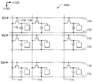
次に、上述した液晶パネル100のうち、素子基板101の電気的な構成について説明する。図2は、この構成を示す概略図である。
【0051】
この図に示されるように、素子基板101には、外部回路からの各種の信号を入力するために複数の実装端子107が設けられている。これらの実装端子107を介して入力される信号は、各種配線を介して各部に供給される構成となっている。そこで、これらの信号について簡単に説明することとする。
【0052】
第1に、VID1〜VID6は、図4に示されるように、ドットクロックDCLKに同期して供給される1系統の画像信号VIDを、6系統に分配するとともに時間軸に6倍に伸長したものであり、6本の画像信号線122を介してサンプリング回路150に供給される。
【0053】
なお、この画像信号VID1〜VID6は、外部回路によって、適宜、極性反転される。ここで、本実施形態における極性反転とは、対向電極108に印加される電圧LCcomを基準として正極性と負極性とに交互に電圧レベルを反転させることをいうが、極性を反転するか否かについては、一般には、データ線への画像信号の印加方式が▲1▼走査線単位の極性反転であるか、▲2▼データ線単位の極性反転であるか、▲3▼画素単位の極性反転であるか、▲4▼フレーム単位の極性反転であるかに応じて定められ、その反転周期は、1水平走査期間、ドットクロックDCLKまたは1垂直走査期間の周期に設定される。ただし、本実施形態では、説明の便宜上、▲1▼走査線単位の極性反転である場合を例にとって説明するが、本発明をこれに限定する趣旨ではない。
【0054】
第2に、VssYおよびVssXは、それぞれ走査線駆動回路130およびデータ線駆動回路140における電源の低位側電圧(接地電位)である。また、VddYおよびVddXは、それぞれ走査線駆動回路130およびデータ線駆動回路140における電源の高位側電圧である。これらのうち、電源の低位側電圧VssYは、後述する蓄積容量の接地電位となっているので、容量線175を介して各画素にも供給されている。
【0055】
第3に、LCcomは、対向電極108に印加される電圧信号である。このため、電圧信号LCcomが供給される2つの電極109は、対向基板102との貼り合わせる際に用いられるシール材104(図1参照)の隅に相当する地点にそれぞれ設けられている。したがって、素子基板101が実際に対向基板102に貼り合わせられると、電極109と対向電極108とが導通材を介して接続されて、対向電極108に電圧信号LCcomが印加される構成となる。なお、電圧信号LCcomは、時間軸に対して一定の電圧であり、外部回路が、この電圧信号LCcomを基準にして、画像信号VID1〜VID6を、1水平走査期間毎に高位側および低位側に振り分けて、交流駆動を行う構成となっている。また、電極109が設けられる地点は、本実施形態においては2箇所であるが、この電極109が設けられる理由は、導通材を介して対向電極108に電圧信号LCcomを印加するためであるから、電極109が設けられる地点は少なくとも1箇所であれば足りる。このため、電極109が設けられる地点は、1箇所でも良いし、3箇所以上であっても良い。
【0056】
第4に、DYは、図4に示されるように、1垂直有効走査期間の最初に供給される転送開始パルスであり、CLYは、走査線駆動回路130において用いられるクロック信号である。なお、CLYinvは、クロック信号CLYをレベル反転させた反転クロック信号である。
【0057】
第5に、DXは、図4に示されるように、1水平有効走査期間の最初に供給される転送開始パルスであり、CLXは、データ線駆動回路140において用いられるクロック信号である。なお、CLXinvは、クロック信号CLXをレベル反転させた反転クロック信号である。また、ENB1、ENB2は、後述するように、データ線駆動回路140におけるシフトレジスタの各出力信号を、所定のパルス幅に制限するために用いられるイネーブル信号である。くわえて、NRGは、プリチャージ制御信号であり、NRSは、プリチャージ電圧信号であるが、詳細については後述することとする。
【0058】
さて、素子基板101の表示領域100aにあっては、複数本の走査線112が行(Y)方向に沿って平行に配列し、また、複数本のデータ線114が列(X)方向に沿って平行に配列して、これらの各交差部分に対応して画素が設けられている。
【0059】
詳細には、図3に示されるように、走査線112とデータ線114とが交差する部分においては、画素を制御するためのスイッチング素子たるTFT116のゲートが走査線112に接続される一方、TFT116のソースがデータ線114に接続されるとともに、TFT116のドレインが矩形状の透明な画素電極118に接続されている。
【0060】
上述したように、液晶パネル100では、素子基板101と対向基板102との電極形成面の間において液晶105が挟持されているので、各画素の液晶容量は、画素電極118と、対向電極108と、これら両電極間に挟持された液晶105とによって構成されることになる。ここで、説明の便宜上、走査線112の総本数を「m」とし、データ線114の総本数を「6n」とすると(m、nは、それぞれ整数とする)、画素は、走査線112とデータ線114との各交差部分に対応して、m行×6n列でマトリクス状に配列することになる。
【0061】
また、表示領域100aには、このほかに、液晶容量のリークを防止するための蓄積容量119が、画素毎に設けられている。この蓄積容量119の一端は、画素電極118(TFT116のドレイン)に接続される一方、その他端は、容量線175により共通接続されている。このため、蓄積容量119は、液晶容量とは電気的に並列となるので、液晶容量の保持特性が改善されて、高コントラスト比の表示が図られることとなる。なお、容量線175には、本実施形態では、電源の低位側電圧VssYが印加される構成であるが、ここには、時間的に一定の電圧が印加されれば良いので、電源の高位側電圧VddYや、電圧LCcomなどが印加される構成であっても良い。また、蓄積容量119を含めた画素の詳細構成については、さらに後述することとする。
【0062】
そこで、説明を再び図2に戻すと、走査線駆動回路130は、水平走査期間1H毎に順次アクティブレベルとなる走査信号G1、G2、…、Gmを、1垂直有効表示期間内に各走査線112に出力するものである。詳細な構成については本発明と直接関連しないので図示を省略するが、シフトレジスタと複数の論理積回路(あるいは否定論理積回路)とから構成される。このうち、シフトレジスタは、図4に示されるように、1垂直有効走査期間の最初に供給される転送開始パルスDYを、クロック信号CLY(および反転クロック信号CLYinv)のレベルが遷移する毎に(立ち上がりおよび立ち下がりの双方で)、順次シフトして、信号G1’、G2’、G3’、…、Gm’として出力し、各論理積回路は、信号G1’、G2’、G3’、…、Gm’のうち、相隣接する信号同士の論理積信号を求めて、走査信号G1、G2、G3、…、Gmとして出力するものである。
【0063】
また、データ線駆動回路140は、順次アクティブレベルとなるサンプリング信号S1、S2、…、Snを1水平有効走査期間内に出力するものである。この詳細な構成についても本発明と直接関連しないので図示を省略するが、シフトレジスタと複数の論理積回路とから構成されている。このうち、シフトレジスタは、図4に示されるように、1水平有効走査期間の最初に供給される転送開始パルスDXを、クロック信号CLX(および反転クロック信号CLXinv)のレベルが遷移する毎に順次シフトして、信号S1’、S2’、S3’、…、Sn’として出力し、各論理積回路は、信号S1’、S2’、S3’、…、Sn’のパルス幅を、イネーブル信号ENB1またはENB2を用いて、相隣接するもの同士が互いに重複しないように、期間SMPaに狭めてサンプリング信号S1、S2、S3、…、Snとして出力するものである。
【0064】
続いて、サンプリング回路150は、データ線114毎に設けられるサンプリングスイッチ151から構成されている。一方、データ線114は6本毎にブロック化されており、図2において左から数えてj(jは、1、2、…、n)番目のブロックに属するデータ線114の6本のうち、最も左に位置するデータ線114の一端に接続されるサンプリングスイッチ151は、画像信号線122を介して供給される画像信号VID1を、サンプリング信号Sjがアクティブとなる期間においてサンプリングして、当該データ線114に供給する構成となっている。また、同じくi番目のブロックに属するデータ線114の6本のうち、2番目に位置するデータ線114の一端に接続されるサンプリングスイッチ151は、画像信号線122を介して供給される画像信号VID2を、サンプリング信号Sjがアクティブとなる期間においてサンプリングして、当該データ線114に供給する構成となっている。
【0065】
以下同様に、j番目のブロックに属するデータ線114の6本のうち、3、4、5、6番目に位置するデータ線114の一端に接続されるサンプリングスイッチ151の各々は、画像信号線122を介して供給される画像信号VID3、VID4、VID5、VID6の各々を、サンプリング信号Sjがアクティブとなる期間においてサンプリングして、対応するデータ線114に供給する構成となっている。すなわち、サンプリング信号Sjがアクティブレベルとなると、i番目のブロックに属する6本のデータ線114の各々には、それぞれ画像信号VID1〜VID6が同時にサンプリングされる構成となっている。
【0066】
一方、表示領域100aを挟んで、データ線駆動回路140とは反対側の領域には、プリチャージ回路160が備えられる。このプリチャージ回路160は、データ線114毎に設けられたプリチャージングスイッチ161からなり、各プリチャージングスイッチ161は、プリチャージ制御線163を介して供給されるプリチャージ制御信号NRGがアクティブレベルとなった場合に、プリチャージ信号線165を介して供給されるプリチャージ電圧信号NRSを、対応するデータ線114にプリチャージする構成となっている。
【0067】
ここで、プリチャージ制御信号NRGは、図5に示されるように、1水平帰線期間のうち、その時間的な前後端から隔絶された期間においてアクティブレベルとなる信号である。また、プリチャージ電圧信号NRSは、同図に示されるように、1水平走査期間1H毎に、電圧LCcomを基準にして電圧Vg+、Vg−でレベル反転する信号である。
【0068】
一方、電圧LCcomは、上述したように対向電極108に印加される時間的に一定の電圧であって、画像信号VID1〜VID6の振幅中心電圧である。また、電圧Vg+、Vg−は、電圧LCcomに対する差電圧の実効値が互いに同一となる(絶対値が等しい)電圧であって、それぞれ電圧LCcomよりも高位側電圧、低位側電圧である。ここで、本実施形態が電圧無印加状態で白色表示を行うノーマリーホワイトモードである場合に、正極側、負極側で黒色表示するために画素電極118に印加すべき電圧をVb+、Vb−とすると、電圧Vg+は、電圧Vb+と電圧LCcomとの中間電圧に設定され、また、電圧Vg−は、電圧Vb−と電圧LCcomとの中間電圧に設定される。すなわち、電圧Vg+、電圧Vb−は、それぞれ正極側、負極側の書込における中間(灰色)電圧に相当するものである。
【0069】
このような構成によるプリチャージ回路160によれば、サンプリング信号S1、S2、S3、…、Snが供給される1水平有効表示期間よりも前の1水平帰線期間において、各データ線114が、電圧Vg+またはVg−に、予めプリチャージされるので、その直後の1水平有効表示期間において、画像信号VID1〜VID6がデータ線114にサンプリングされる際の負荷が低減されることとなる。
【0070】
なお、これらの走査線駆動回路130や、データ線駆動回路140、サンプリング回路150、プリチャージ回路160などは、製造後に欠陥の有無を判別するための検査回路とともに、表示領域100aの周辺に形成されるので、周辺回路として呼称されるものである。ただし、検査回路については、本件とは直接関係しないので、その説明については省略することとする。
【0071】
<電気光学装置の動作>
次に、上述した構成に係る電気光学装置の動作について説明する。ここでまず、走査信号G1がアクティブレベルとなる1水平走査期間1Hについて着目する。なお、この1水平走査期間では、説明の便宜上、正極側の書込を行うものとすると、画像信号VID1〜VID6は、対向電極108に印加される電圧LCcomに対して高位側電圧となる。
【0072】
またこれに先立って、プリチャージ制御信号NRGが、図5に示されるように、その帰線期間の前後端から隔絶された期間にてアクティブレベルとなる。この際、プリチャージ電圧信号NRSは、正極側の書込に対応して電圧Vg+となる。このため、当該期間において、すべてのデータ線114が電圧Vg+にプリチャージされることとなる。
【0073】
次に、1水平帰線期間が終了して、1水平有効表示期間になると、その最初に転送開始パルスDXが、図4または図5に示されるように、データ線駆動回路140に供給される。この転送開始パルスDXは、クロック信号CLXのレベルが遷移する毎に順次シフトされた信号S1’、S2’、S3’、…、Sn’として出力される。そして、この信号S1’、S2’、S3’、…、Sn’の各パルス幅が、相隣接するもの同士が互いに重複しないように期間SMPaに狭められて、サンプリング信号S1、S2、S3、…、Snとして出力される。
【0074】
一方、1系統の画像信号VIDは、外部回路によって、図4に示されるように、画像信号VID1〜VID6に分配されるとともに、時間軸に対して6倍に伸長されて、液晶パネル100に供給される。
【0075】
ここで、走査信号G1がアクティブレベルとなる期間において、サンプリング信号S1がアクティブレベルとなると、図2において上から数えて1本目のTFT116がすべてオンになるとともに、左から1番目のブロックに属する6本のデータ線114に、それぞれ画像信号VID1〜VID6がサンプリングされる。そして、サンプリングされた画像信号VID1〜VID6は、当該1本目の走査線112と当該6本のデータ線114と交差する画素のTFT116によって、それぞれ対応する画素電極118に印加されることとなる。
【0076】
この後、サンプリング信号S2がアクティブレベルとなると、今度は、2番目のブロックに属する6本のデータ線114に、それぞれ画像信号VID1〜VID6がサンプリングされて、これらの画像信号VID1〜VID6が、当該1本目の走査線112と当該6本のデータ線114と交差する画素のTFT116によって、それぞれ対応する画素電極118に印加されることとなる。
【0077】
以下同様にして、サンプリング信号S3、S4、……、Snが順次アクティブレベルとなると、第3番目、第4番目、…、第n番目のブロックに属する6本のデータ線114にそれぞれ画像信号VID1〜VID6がサンプリングされ、これらの画像信号VID1〜VID6が、当該1本目の走査線112と、当該6本のデータ線114と交差する画素のTFT116によって、それぞれ対応する画素電極118に印加されることとなる。これにより、第1行目の画素のすべてに対する書込が完了することになる。
【0078】
続いて、走査信号G2がアクティブとなる期間について説明する。本実施形態では、上述したように、走査線単位の極性反転が行われるので、この1水平走査期間においては、負極側の書込が行われることとなる。このため、画像信号VID1〜VID6は、対向電極108に印加される電圧LCcomに対して低位側電圧となる。これに先だって、帰線期間におけるプリチャージ電圧信号NRSの電圧はVg−となるので、プリチャージ制御信号NRGがアクティブレベルとなった場合に、すべてのデータ線114は、電圧Vg−にプリチャージされることとなる。
【0079】
他の動作については同様であり、サンプリング信号S1、S2、S3、…、Snが順次アクティブレベルとなって、第2行目の画素のすべてに対する書込が完了することになる。
【0080】
以下同様にして、走査信号G3、G4、…、Gmがアクティブとなって、第3行目、第4行目、…、第m行目の画素に対して書込が行われることとなる。これにより、奇数行目の画素については正極側の書込が行われる一方、偶数行目の画素については負極側の書込が行われて、この1垂直走査期間においては、第1行目〜第m行目の画素のすべてにわたった書込が完了することになる。
【0081】
そして、次の1垂直走査期間においても、同様な書込が行われるが、この際、各行の画素に対する書込極性が入れ換えられる。すなわち、次の1垂直走査期間において、奇数行目の画素については負極側の画素に対して書込が行われる一方、偶数行目の画素については正極側の書込が行われることとなる。
【0082】
このように、1垂直走査期間毎に画素に対する書込極性が入れ換えられので、液晶105に直流成分が印加されることがなくなって、その劣化が防止されている。
【0083】
また、このような駆動では、データ線114を1本毎に駆動する方式と比較すると、各サンプリングスイッチ151によって画像信号をサンプリングする時間が6倍となるので、各画素における書込み電時間が十分に確保される。このため、高コントラスト比が得られることになる。さらに、データ線駆動回路140におけるシフトレジスタの段数、および、クロック信号CLXの周波数が、それぞれ1/6に低減されるので、段数の低減化と併せて低消費電力化も図られることとなる。
【0084】
さらに、サンプリング信号S1、S2、…、Snのアクティブ期間は、クロック信号CLXの半周期よりも狭められて、期間SMPaに制限されているので、隣接するサンプリング信号同士のオーバーラップが事前に防止される。このため、あるブロックに属する6本のデータ線114にサンプリングされるべき画像信号VID1〜VID6が、これに隣接するブロックに属する6本のデータ線114にも同時サンプリングされる事態が防止されて、高品位な表示が可能となっている。
【0085】
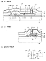
<画素の詳細構成>
次に、画素の詳細について図6および図7を参照して説明する。図6は、画素部の詳細構成を示す平面図であり、図7(a)は、図6におけるB−B’線の断面図である。なお、図6において、最上導電層となる画素電極118については、説明理解のために、その輪郭だけを破線により示すことにする。
【0086】
まず、図7(a)に示されるように、素子基板101の基材たる基板10には、下地絶縁膜40を介してポリシリコンからなる半導体層30が設けられ、その表面は、熱酸化による絶縁膜32で覆われている。
【0087】
一方、図6に示されるように、データ線114はY方向に延在し、走査線112はX方向に延在している。また、容量線175は、走査線112と近接して平行に設けられているが、データ線114と交差する部分においては、データ線114と重なるように、前段側(図6において上側)に突出して形成されている。
【0088】
ここで、半導体層30は、データ線114および容量線175が交差する部分から、容量線175の延在方向(図6において右方向)、データ線114の下層における容量線175の突出方向(同、上方向)、および、その反対方向(同、下方向)の計3方向に延設して略T字状に、かつ、これらの配線で覆われるように形成されている。
【0089】
さらに、半導体層30のうち、走査線112と重なる部分がチャネル領域30aとなっている。換言すれば、走査線112のうち、半導体層30と交差する部分がゲート電極116Gとして用いられている。なお、ゲート電極116Gを含む走査線112および容量線175は、後述するように例えばポリシリコン等から形成されている。
【0090】
また、半導体層30において、チャネル領域30aのソース側には、低濃度(翻訳はlightly dopedで表現する)ソース領域30b、高濃度(翻訳はheavily dopedで表現する)ソース領域116Sが設けられる一方、ドレイン側には、低濃度ドレイン領域30c、高濃度ドレイン領域116Dが設けられて、いわゆるLDD(Lightly Doped Drain)構造となっている。
【0091】
このうち、高濃度ソース領域116Sは、絶縁膜32、第1の層間絶縁膜41および第2の層間絶縁膜42を開孔するコンタクトホール52によって、アルミニウム等からなるデータ線114に接続されている。
【0092】
一方、高濃度ドレイン領域116Dは、絶縁膜32および第1の層間絶縁膜41を開孔するコンタクトホール51によって、高融点金属やポリシリコン等からなる中間導電膜181の一端に接続されている。一方、この中間導電膜181の他端は、第2の層間絶縁膜42および第3の層間絶縁膜43を開孔するコンタクトホール53によって、画素電極118に接続されている。すなわち、画素電極118は、中間導電膜181を介して、TFT116の高濃度ドレイン領域116Dに接続されている。
【0093】
ここで、画素電極118を高濃度ドレイン領域116Dに直接的に接続せずに、中間導電膜181を介して間接的に接続する構成としたのは、次のような理由による。すなわち、画素電極118は、液晶容量に電圧を印加するための電極であるから、液晶105に近い部分に形成され、反対に半導体層30は遠い部分に形成される。さらに、半導体層30と画素電極118との間には、本実施形態のようにTFT116がプレーナ型であれば、走査線112やデータ線114などの配線層が層間絶縁膜を介して積層されるので、半導体層30と画素電極118との距離は必然的に大きくなる。このため、画素電極118を高濃度ドレイン領域116Dに直接的に接続する構成では、比較的深さのあるコンタクトホールを例えばドライエッチングにより形成しなければならない。ただし、このような深さのあるコンタクトホールを形成する際に、過剰にエッチングしてしまうと、半導体層30を突き破ってしまう、という不具合が発生する。特に、半導体層30と絶縁膜との選択比に大差がなく、さらには、半導体層30の膜厚が、エッチングすべき絶縁膜の厚さに比べて極めて薄いという事情は、かかるコンタクトホールを設けることを、より困難にさせている。
【0094】
そこで、第1に、高濃度ドレイン領域116Dの対応位置にコンタクトホール51を設けて、絶縁膜32および第1の層間絶縁膜41を開孔し、第2に、このコンタクトホール51を介して電気的に接続される中間導電膜181を形成して、この中間導電膜181を高濃度ドレイン領域116Dのバリア膜として機能させているのである。これにより、画素電極118形成前にコンタクトホール53を開孔する際に、中間導電膜181をエッチングストッパーとして用いることによって、過剰エッチングによる半導体層30の突き破りを防止しているのである。
【0095】
さて、この中間導電膜181は、特に図6に示されるように、隣接するデータ線114の間において容量線175をほぼ覆うとともに、その一部が走査線112にかかっている(ただし電気的には絶縁されている)。さらに、画素電極118が形成されない領域は、Y方向ではデータ線114で覆われ、X方向では走査線112および中間導電膜181で覆われている。ここで中間導電層181としてはポリシリコンでも良し、Ti(チタン)、Cr(クロム)、W(タングステン)、Ta(タンタル)、Mo(モリブデン)又はPb(鉛)の単体若しくはこれらの合金、金属シリサイドでも良い。したがって、画素部での遮光領域は、データ線114、走査線112および中間導電膜181により完全に規定されるので、対向基板102に別途設けられていた遮光膜を省略することが可能となる。くわえて、半導体層30は、データ線114、走査線112、容量線175および中間導電膜で覆われているので、基板の上側からの光がTFT116に侵入するのが防止されることになる。また、半導体層30の下側であって、基板10および下地絶縁膜40の間に遮光膜を形成しても良い。これにより、基板の下側からの光がTFT116に侵入することを防止することができるため、光照射によるTFT116の特性変化の防止が図られている。
【0096】
次に、蓄積容量119の詳細構成について、図6および図7(a)にくわえて、図7(b)および同図(c)をも参照して説明する。ここで、図7(b)は、図6におけるC−C’線の断面図であり、図7(c)は、蓄積容量119の等価回路を示す図である。
【0097】
まず、半導体層30のうち、高濃度ドレイン領域116Dに隣接する領域30fは、高濃度のドーピングにより低抵抗化されて、平面的には、容量線175の下層において略L字形状となっている。一方、中間導電膜181は、容量線175とは第1の層間絶縁膜41を介して、かつ、上述したようにX方向において容量線175を覆うように形成されている。したがって、蓄積容量119は、図7(b)または同図(c)に示されるように、2つの容量を並列化したものとなる。詳細には、蓄積容量119は、領域30fを一方の電極とし、容量線175を他方の電極として、半導体層30の表面に形成された絶縁膜32を挟持してなる第1の容量と、中間導電膜181を一方の電極とし、容量線175を他方の電極として、第1の層間絶縁膜41を挟持してなる第2の容量との並列接続により構成されている。このため、蓄積容量119は、単一の容量からなる場合と比較して容量増加するので、液晶容量の保持特性が改善されて、表示の高品位化が図られることになる。
【0098】
なお、最上層(すなわち、液晶108と接する面)の全面には、ポリイミド等の有機膜からなる配向膜61が形成されて、対向基板102との貼り合わせ前に、ラビング処理が施される。
【0099】
<周辺回路の詳細構成>
次に、周辺回路の詳細について、サンプリング回路150の一部領域と、走査線駆動回路130の一部領域とを例にとってそれぞれ説明する。なお、周辺回路を構成する能動素子や配線は、後の製造プロセスで詳述するように、表示領域におけるTFT116や、走査線112(および容量線175)、中間導電膜181、データ線114と共通プロセスで形成される。
【0100】
このうち、表示領域101aにおいて、配線は、走査線112(および容量線175)、中間導電膜181、データ線114の順番で形成されるので、以下の説明では、周辺回路における配線のうち、走査線112を構成する導電層と同一層からなる配線を第1層の配線と呼称し、また、中間導電膜181を構成する導電層と同一層からなる配線を第2層の配線と呼称し、さらに、データ線114を構成する導電層と同一層からなる配線を第3層の配線と呼称することとする。なお、中間導電膜181を構成する導電層は、従来では周辺回路領域に用いられていなかったので、本実施形態における第3層の配線は、従来の電気光学装置における第2層の配線に相当することになる。
【0101】
このように、周辺回路において第1層から第3層までの3層分の配線を用いると、周辺回路を設計する際の自由度が、2層分の配線しか用いていなかった従来よりも、各段に向上する。さらに、第2層の配線を次に述べるように用いることによって、配線抵抗の低減化や、回路形成領域の縮小化を図ることが可能となる。
【0102】
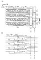
<サンプリング回路の近傍領域>
そこでまず、サンプリング回路150の一部領域について、図8(a)および同図(b)を参照して説明する。なお、ここでは、左からj番目のブロックに対応して出力されるサンプリング信号Sjと、6本の画像信号線122から当該ブロックに属する6本のデータ線114に至るまでの経路との関係を中心にして説明することとする。なお、jは、図2の説明と同様にブロックを一般化して説明するためのものであって、本実施形態では「1」から「n」までのいずれかの整数である。
【0103】
図8(a)は、この領域の詳細構成を示す平面図である。まず、データ線駆動回路140から出力されるサンプリング信号Sjは、第3層の配線391、下層の配線191、第3層の配線393および6個の第1層の配線412という経路で供給される。ここで、各配線同士は、コンタクトホールを介して接続され、また、第1層の配線412は、そのままサンプリングスイッチ151を構成するTFTのゲート電極となっている。
【0104】
一方、画像信号VID1〜VID6のうち、画像信号VID1は、次のような経路でサンプリングスイッチ151に供給されている。すなわち、画像信号VID1は、第3層からなる画像信号線122、下層の配線193、第3層の配線395、下層の配線195および第3層の配線397という経路を介して、サンプリングスイッチ151を構成するTFTのソース領域に供給されている。他の画像信号VID2〜VID6についても同様な経路を介して、サンプリングスイッチ151を構成するTFTのソース領域に供給されている。そして、各サンプリングスイッチ151を構成するTFTのドレイン領域には、それぞれ第3層のデータ線114が接続されている。
【0105】
このようにサンプリング回路150の各種配線には原則として第3層の配線が用いられるが、この第3層の配線と交差する部分およびゲート電極として用いられる部分には例外として下層の配線が用いられている。
【0106】
ここで、図8(a)におけるD−D’線の断面構造について、図8(b)を参照して説明する。この図に示されるように、画像信号VID1が供給される画像信号線122から分岐して、他の画像信号線122とは下層において交差する配線193は、第1層の配線112bと第2層の配線181bとが並列接続された並列配線となっている。詳細には、配線181bは、その両端において第1の層間絶縁膜41を開孔するコンタクトホール551、561を介して配線112bと並列接続されている。さらに、画像信号VID1が供給される画像信号線122は、コンタクトホール551と同位置に設けられたコンタクトホール552を介して配線181bと接続される一方、配線395は、コンタクトホール561と同位置に設けられたコンタクトホール562を介して配線181bと接続されている。
【0107】
なお、画像信号VID1以外の他の画像信号VID2〜VID6が供給される画像信号線122から分岐する配線193についても、同様に第1層の配線112bと第2層の配線181bとが並列接続された並列配線となっている。さらに、画像信号線122から分岐・交差する配線193のほか、サンプリング信号Sjが供給される配線393と交差するための配線195についても、同様に第1層の配線112cと第2層の配線181cとが並列接続された並列配線となっている。
【0108】
ここで、サンプリング回路150において、配線193、195に、第1層の配線と第2層の配線との並列配線を用いているのは、次の理由による。すなわち、画像信号VID1〜VID6は、画素電極118に最終的に印加されて表示状態を直接的に規定するアナログ信号であるので、その供給経路は、少しでも低抵抗であるのが望ましい。このため、画像信号線122についてはアルミニウムからなる第3層が用いられるが、ここから分岐する配線については、一部どうしても第3層以外の層を用いなければならない。このため、従来では、この部分には、走査線112を構成する導電層からなる配線、すなわち、第1層の配線が用いられていた。しかし、第1層は、上述したようにポリシリコン等であるので、第3層を構成するアルミニウム等と比較して、遙かに高抵抗である。このため、第1層の配線長がごくわずかであっても、その抵抗分による影響は無視できない程に大きい。
【0109】
そこで、本実施形態では、画像信号VID1〜VID6の供給経路のうち、第3層以外の層からなる配線を用いなければならない部分には、本来、表示領域で用いられていた第2層を周辺回路領域においても用いるとともに、この第2層からなる配線と、第1層の配線とを並列接続しているのである。このため、当該部分の抵抗値は、単一層の配線からなる場合と比較して、約半分程度にまで低減されることになる。したがって、本実施形態では、画像信号VID1〜VID6は、供給経路における波形鈍化や電圧降下等が防止された上で、データ線114に供給されるので、良好な表示が可能となる。
【0110】
なお、画像信号線122から分岐する並列配線193は、図8(a)に示されるように、画像信号VID1〜VID6のそれぞれにわたって、略同一長・略同一幅となっている。これは、本実施形態では、配線193が第1層の配線112bと第2層の配線181bとの並列接続から構成されて、その配線抵抗が低減されてはいるものの、第3層の配線と比較すれば依然として大きいので、配線193の抵抗値が、画像信号VID1〜VID6のそれぞれにわたって互いに等しくするための措置である。
【0111】
また、画像信号VID1〜VID6の供給経路から外れるが、サンプリング信号Sjを画像信号線122と交差するために供給する配線191についても、同様に第1層の配線と第2層の配線との並列接続となっている。これは、サンプリング信号Sjの波形鈍化等による遅延防止の観点から、サンプリング信号Sjの供給経路についても、少しでも低抵抗であることが要請されているからである。
【0112】
このように、本実施形態において、サンプリング回路150の各種配線には、原則として低抵抗な第3層の配線が用いられる一方、第3層の配線と交差しなければならない部分には、第1層の配線と第2層の配線との並列配線が用いられている。ここで、周辺回路全体でみれば、このように並列配線を用いるべき部分は、サンプリング回路150における配線191、193、195のほかにも多数存在する。例えば、図2におけるプリチャージ制御線163は、各プリチャージングスイッチ161を構成するTFTのゲート電極にそれぞれ分岐しなければならないが、分岐後、プリチャージ電圧信号線165と交差しなければならない部分が存在する。また、容量線175は、表示領域100a内においては走査線112と同じ第1層の配線であるが、それ以外の領域においては、実装端子107から引き回して共通接続することとの関係上、第3層の配線で構成されなければならない。このような容量線175に対して、プリチャージ制御線163、プリチャージ電圧信号線165は、図2に示されるように交差しなければならない部分が存在する。さらに、走査線駆動回路130において、シフトレジスタを構成する単位回路には、電源電圧VddY、VssYとともに、クロック信号CLYおよび反転クロック信号CLYinvを供給する必要がある。このため、クロック信号CLYおよび反転クロック信号CLYinvの基幹配線から分岐する配線については、少なくとも電源電圧VddY、VssYが供給される配線と交差しなければならない部分が存在する。同様に、データ線駆動回路140において、シフトレジスタを構成する単位回路には、電源電圧VddX、VssXとともに、クロック信号CLXおよび反転クロック信号CLXinvを、各論理積回路には、電源電圧VddX、VssXとともに、イネーブル信号ENB1、ENB2を、それぞれ供給する必要がある。このため、クロック信号CLXおよび反転クロック信号CLXinvの基幹配線から分岐する配線と、イネーブル信号ENB1、ENB2の基幹配線から分岐する配線とについては、それぞれ、少なくとも電源電圧VddY、VssYが供給される配線と交差しなければならない部分が存在する。そして、このように第3層の配線と交差しなければならない部分に、第1層の配線と第2層の配線とを並列接続した並列配線を用いることで、当該部分の低抵抗化を図ることが可能となる。
【0113】
<走査線駆動回路の一部領域>
続いて、走査線駆動回路130の一部領域について図9(a)および同図(b)を参照して説明する。ここで、図9(a)は、走査線駆動回路130の一部領域の構成を示す平面図であり、同図(b)は、その等価回路を示す図である。なお、図に示される領域は、走査線駆動回路130を構成するシフトレジスタのうち、転送開始パルスDYをクロック信号CLYおよび反転クロック信号CLYinvにしたがって転送するための回路を部分的に抜き出したものである。
【0114】
図9(a)に示されるように、走査線駆動回路130には、第1層、第2層、第3層の配線が用いられている。そして、この領域においても、原則として第3層の配線が用いられているが、例外として、第3層の配線と交差する部分およびゲート電極として用いられる部分には、第1層の配線が用いられ、また、一方のTFTのソース電極から他方のTFTのドレイン電極に至る配線の一部には、第2層の配線181dが用いられている。特に、領域132では、第1層の配線112d、第2層の配線181dおよび第3層の配線114dが互いに層間絶縁膜(ここでは図示省略)を介し積層されて形成されている。
【0115】
ここで、走査線駆動回路130において、上述したサンプリング回路150とは異なり、第2層の配線181dを単独で用いるとともに、3層の配線を同一領域に形成しているのは、次の理由による。すなわち、データ線駆動回路130は、サンプリング信号S1、S2、…、Snを、それぞれ6本のデータ線114毎に供給するので、データ線駆動回路130を構成するシフトレジスタの単位回路や論理積回路については、図8(a)におけるデータ線ピッチの6倍のピッチ内に収めれば済む。これに対し、走査線駆動回路130は、走査信号G1、G2、…、Gmをm本の走査線112の各々に対してそれぞれ供給しなければならないので、走査線駆動回路140を構成するシフトレジスタの単位回路や論理積回路については、図9(a)における走査線ピッチと等倍のピッチ内に収めなければならない。すなわち、走査線駆動回路130では、その単位回路や論理積回路を、データ線駆動回路140と比較して、より狭い領域内において形成しなければならない。ここで仮に、第2層の配線181dを用いないで、3つの配線を、第1層および第3層のみから形成する場合、1つの配線を第1層から、残りの2つの配線を第3層から、それぞれ形成しなければならないが、この場合、同一領域において、第3層の配線を2つ重ねて形成するのは不可能である。このため、異なる領域において、第3層の配線を並べて形成するほかないので、それだけ幅広の領域を必要とすることになる。したがって、このような構成では、走査線駆動回路130を構成する単位回路や論理積回路を、より狭い領域内において形成しなければならないという要請に反することになる。これに対し、本実施形態では、第2層の配線181dを単独で用いて、同一の領域132において第1層の配線112d、第2層の配線181dおよび第3層の配線114dを、(層間絶縁膜を介して絶縁を図った上で)互いに重ねて形成することによって、回路形成に必要な領域の幅を小さくすることができることとなる。
【0116】
なお、走査線駆動回路130においては、回路形成に必要な領域の幅が狭いことを要求されない部分であって、第3層の配線と交差しなければならない部分には、第1層の配線と第2層の配線との並列配線を用いても良いのは、もちろんである。
【0117】
<製造プロセス>
次に、本実施形態に係る電気光学装置の製造プロセスについて、素子基板101の表示領域と周辺回路領域とを中心にして説明する。なお、ここいう周辺回路領域としては、図8(b)において、ある1本の画像信号線122から分岐して、他の画像信号線122と交差する配線193の近傍領域を例示することとする。
【0118】
まず、図10(1)に示されるように、例えば、石英基板や、ガラス基板、シリコン基板等の基板10の表面に、下地絶縁膜40を形成する。詳細には、下地絶縁膜40は、例えば常圧法や減圧CVD(Chemical Vapor Deposition)法などにより、NSG(ノンドープトシリケートガラス)や、PSG(リンシリケートガラス)、BSG(ボロンシリケートガラス)、BPSG(ボロンリンシリケートガラス)などの高絶縁性ガラス、または、酸化シリコン膜、窒化シリコン膜等から、約50〜1500nmの厚さで、好ましくは約600〜800nm程度の厚さで形成される。
【0119】
引き続き、下地絶縁膜40の上面全体に、例えば減圧CVD法などによって、アモルファスシリコン層を約100nmの厚さで形成し、熱処理等により固相成長させることによってポリシリコン層を形成する。この際、Nチャネル型のTFTを形成する場合には、Sb(アンチモン)や、As(砒素)、P(リン)などのV属元素の不純物を、わずかにイオン注入等によりドーピングする一方、Pチャネル型TFTを形成する場合には、Al(アルミニウム)や、B(ボロン)、Ga(ガリウム)などのIII属元素の不純物を、同様に、わずかにイオン注入等によりドーピングする。そして、同図(2)に示されるように、ポリシリコン層を、フォトリソグラフィやエッチング等によってパターニングして、表示領域におけるTFT116の半導体層30を島状に形成する。なお、この際、周辺回路全体においては、走査線駆動回路130や、データ線駆動回路140、サンプリング回路150、プリチャージ回路160を構成するTFTの半導体層についても同様に形成する。また、TFT116の半導体層30のうち、容量線175が形成される領域30fについては、P(リン)などの不純物を高濃度でドーピングして、予め低抵抗化を図っておいても良い。
【0120】
さらに、図10(3)に示されるように、半導体層30の表面を熱酸化処理して、ゲート絶縁膜32を当該半導体層30の表面に形成する。この工程により、半導体層30は最終的に約30〜150nmの厚さ、好ましくは約35〜45nmの厚さとなる一方、ゲート絶縁膜32は約60〜150nmの厚さ、好ましくは約30nmの厚さとなる。
【0121】
次に、ゲート絶縁膜32および下地絶縁膜40の上面に、ポリシリコン層を減圧CVD法等により堆積する。そして、図11(4)に示されるように、このポリシリコン層を、フォトリソグラフィやエッチング等によってパターニングして、表示領域にあってはTFT116のゲート電極を兼用する走査線112と、蓄積容量119において他方の電極をなす容量線175とを形成し、また、周辺回路領域にあっては並列配線193のうち一方の配線112bを形成する。すなわち、周辺回路全体では、ゲート電極を含めて第1層の配線を形成する。
【0122】
続いて、同図(5)に示されるように、半導体層30に適切な不純物をドーピングする。詳細には、表示領域におけるTFT116をNチャネル型とする場合、ソース・ドレイン領域のうち、チャネル領域30aに隣接する領域に対し、走査線112の一部であるゲート電極を拡散マスクとして、PなどのV族元素の不純物を低濃度でドーピングする。同時に、周辺回路全体におけるNチャネル型TFTについても、同様に第1層の配線の一部であるゲート電極を拡散マスクとして、不純物を低濃度でドーピングする。続いて、ゲート電極よりも幅広のレジストを形成し、これをマスクとして、同じくPなどのV族元素の不純物を高濃度でドーピングする。これによりNチャネル型TFTは、チャネル領域30aのソース側には、低濃度ソース領域30b、高濃度ソース領域116Sが設けられる一方、ドレイン側には、低濃度ドレイン領域30c、高濃度ドレイン領域116Dが設けられて、LDD構造となる。なお、図示は省略するが、これらのNチャネル型TFTの半導体層30をレジストでマスクした後、周辺回路全体におけるPチャネル型TFTについても同様に、チャネル領域に隣接する領域に対し、第1層の配線の一部であるゲート電極をマスクとして、例えばB(ボロン)などのIII族元素の不純物をドーピングして低濃度領域を形成し、引き続き、同ゲート電極よりも幅広のレジストをマスクとして、同じくBなどのIII族元素の不純物をドーピングして高濃度領域を形成する。また、各チャネル型TFTをLDD構造としないで、オフセット構造のTFTとしても良く、また、単なるセルフアライン型(自己整合型)のTFTとしても良い。
【0123】
次に、同図(6)に示されるように、走査線112や、第1層の配線112b、半導体層30、下地絶縁膜40などを覆うように、第1の層間絶縁膜41を、例えばCVD法等によって堆積する。なお、第1の層間絶縁膜41の材質としては、下地絶縁膜40と同様に、NSGや、PSG、BSG、BPSGなどのシリケートガラス膜や、窒化シリコン膜、酸化シリコン膜などが挙げられる。
【0124】
さらに、図12(7)に示されるように、表示領域にあってはコンタクトホール51を、周辺回路領域にあっては第1層の配線112bと接続するためのコンタクトホール551、561を、それぞれドライエッチング等により形成する。詳細には、コンタクトホール51は、TFT116の高濃度ドレイン領域116Dに対応した位置において、第1の層間絶縁膜41およびゲート絶縁膜32を開孔するように形成される一方、コンタクトホール551、561は、第1層の配線112bの両端位置において、それぞれ第1の層間絶縁膜41を開孔するように形成される。なお、周辺回路全体において、第1層の配線と第2層の配線との導通を図る場合には、この導通部分に対応して同様にコンタクトホール(図示省略)が形成される。
【0125】
次に、第1の層間絶縁膜41の上に、高融点金属や金属シリサイドやあるいはポリシリコンなどからなる導電層を、スパッタリングなどによって約50〜500nmの厚さで、好ましくは約200nm程度の厚さで堆積する。導電層は高融点金属や金属シリサイドとポリシリコンを多層に形成しても良いことは言うまでもない。これにより導電層の応力緩和やコンタクトホールの低抵抗化を実現することができる。そして、この導電層を、同図(8)に示されるように、フォトリソグラフィやエッチング等によってパターニングして、表示領域にあっては、TFT116の高濃度ドレイン領域116Dに接続される中間導電膜181として形成する一方、周辺回路領域にあっては、並列配線193のうち他方の配線181bを形成する。すなわち、周辺回路全体では、第2層の配線を形成する。
【0126】
続いて、同図(9)に示されるように、中間導電膜181や、第2層の配線18b、第1の層間絶縁膜41を覆うように、第2の層間絶縁膜42を、CVD法等によって約500〜1500nmの厚さに堆積する。なお、第2の層間絶縁膜42の材質としては、下地絶縁膜40や第1の層間絶縁膜41と同様に、NSGや、PSG、BSG、BPSGなどのシリケートガラス膜や、窒化シリコン膜、酸化シリコン膜などが挙げられる。
【0127】
次に、図13(10)に示されるように、表示領域にあってはコンタクトホール52を、周辺回路領域にあっては第2層の配線181bと接続するためのコンタクトホール552、562を、それぞれ形成する。詳細には、コンタクトホール52は、TFT116の高濃度ソース領域116Sに対応した位置において、第2の層間絶縁膜42、第1の層間絶縁膜41およびゲート絶縁膜32を開孔するように形成される一方、コンタクトホール552、562は、第2層の配線181bの両端位置において、それぞれ第2の層間絶縁膜42を開孔するように形成される。なお、周辺回路全体において、第2層の配線と第3層の配線との導通を図る場合には、この導通部分に対応して同様にコンタクトホール(図示省略)が形成される。
【0128】
さらに、コンタクトホール52、552、562が形成された第2の層間絶縁膜42の上に、アルミニウムなどの低抵抗金属からなる導電膜を、スパッタリングなどによって、約50〜500nmの厚さに堆積する。そして、この導電膜を、同図(11)に示されるように、フォトリソグラフィやエッチング等によってパターニングして、表示領域にあってはTFT116のソース電極を兼用するデータ線114として形成する一方、周辺回路領域にあっては配線391や画像信号線122として形成する。すなわち、周辺回路全体では、第3層の配線を形成する。
【0129】
引き続き、同図(12)に示されるように、データ線114や、画像信号線122等の第3層の配線を覆うように、第3の層間絶縁膜43を、CVD法等によって約500〜1500nmの厚さに堆積する。なお、第3の層間絶縁膜43の材質としては、下地絶縁膜40や、第1の層間絶縁膜41、第2の層間絶縁膜42と同様に、NSGや、PSG、BSG、BPSGなどのシリケートガラス膜や、窒化シリコン膜、酸化シリコン膜などが挙げられる。
【0130】
次に、図14(13)に示されるように、コンタクトホール53を、中間導電膜181における所定の位置において、第3の層間絶縁膜43および、第2の層間絶縁膜42を開孔するように、ドライエッチング等により形成する。
【0131】
そして、コンタクトホール53が形成された第3の層間絶縁膜42の表面に、ITOなどの透明導電性膜を、スパッタリングなどによって約50〜200nmの厚さに堆積した後、フォトリソグラフィやエッチング等によって所定の形状(図5参照)にパターニングして、同図(14)に示されるように、画素電極118を形成する。この後の工程については図示を省略するが、ポリイミドなどの有機溶液を、基板10において対向面となる画素電極118および第3の層間絶縁膜43の全面に塗布・焼成する。これにより、配向膜61が形成されることとなる。なお、この配向膜61には、所定の方向にラビング処理が施される。
【0132】
そして、このように形成された素子基板101は、それとは約90度回転させた方向にラビング処理された対向基板102と、シール材104により貼り合わせられた後に、液晶105が封入・封止されて、図1に示されるような電気光学装置となる。
【0133】
なお、素子基板101においては、配向膜61が全面にわたって形成されるが、液晶封止後ではプラズマ処理等により、周辺回路領域であって、対向基板102から張り出した部分に形成された配向膜が除去される。このため、周辺回路領域における最上層は、配向膜61ではなく、第3の層間絶縁膜43となる。
【0134】
このような製造方法によれば、表示領域において、TFT116の高濃度ドレイン領域116Dに対するバリア膜として用いられていた中間導電膜181と同一層の導電膜を、周辺回路における第2層の配線として用いることが、特別なプロセスを追加することなく可能となる。さらに、3層分の配線を用いることによって、周辺回路の設計における自由度を各段に向上させることが可能となる。くわえて、第1層の配線とともに並列接続することで、当該配線の低抵抗化を図ることが可能となり、また、第2層の配線を、単独で用いることによって、同一領域において3層の配線を形成することが可能となる。
【0135】
<応用例>
なお、上述した実施形態において、第3層の配線が第1層の配線と第2層の配線との並列配線に接続される場合、当該第3層の配線は、第2層の配線に接続される構成となっていた。例えば、図8(b)において、画像信号線122は、並列配線193のうち、第2層の配線181bに接続される構成となっていた。
【0136】
上述したように、第2層の導電層は、応力の発生しやすい(反りやすい)高融点金属等から構成する場合、このような高融点金属の配線181bに接続するためのコンタクトホール552、562を開孔すると、開孔に伴う応力集中によって第2の層間絶縁膜42にクラック等が発生する可能性がある。また、コンタクトホール552、562によって、第2層の配線181bを露出させると、当該配線181bから不純物が発散して、不良化の原因にもなる。
【0137】
そこで、第3層の配線を第1層の配線112bと第2層の配線181bとの並列配線193の一端に接続する場合には、例えば図15(a)に示されるように、第2層の配線181bを、若干内側のコンタクトホール571、581を介し第1の配線112bに接続して、並列配線193とするとともに、第3層の配線を、外側のコンタクトホール572または582を介して第1層の配線112bに接続する構成が望ましい、と考える。この構成では、第2の層間絶縁膜42が形成された後においては、第2層の配線181bが露出することはない。このため、コンタクトホールの開孔に伴う応力集中が発生しないので、第2の層間絶縁膜42におけるクラックが防止され、また、当該配線181bから不純物が発散することも防止されることになる。
【0138】
さらに、並列配線193は、第1の配線112bおよび第2の配線181bの両端においてのみ接続を図る構成であったが、図15(b)に示されるように、両端以外の1以上の地点にコンタクトホール58、59を設けて、この地点においても接続して、両配線の接続をより確実とする構成にしても良い。なお、このように第1の配線112bと第2の配線181bとの接続を、両端以外の1以上のコンタクトホールを介して図る構成においても、第3層の配線を、外側のコンタクトホールを介して第1層の配線112bに接続しても良い。
【0139】
<その他>
また、上述した実施形態にあっては、6本のデータ線114が1ブロックにまとめられて、1ブロックに属する6本のデータ線114に対して、6系統に変換された画像信号VID1〜VID6を同時にサンプリングして供給する構成としたが、変換数および同時に印加するデータ線数(すなわち、1ブロックを構成するデータ線数)は、「6」に限られるものではない。例えば、サンプリング回路150におけるサンプリングスイッチ151の応答速度が十分に高いのであれば、画像信号をパラレルに変換することなく1本の画像信号線にシリアル伝送して、データ線114毎に点順次的にサンプリングするように構成しても良い。なお、このような構成では、データ線駆動回路140を構成するシフトレジスタや論理積回路を、データ線ピッチと等倍で形成しなければならないので、走査線駆動回路130と同様に、第2層の配線を単独で用いる必要があるかもしれない。
【0140】
また、変換および同時に印加するデータ線の数を「3」や、「12」、「24」等として、3本や、12本、24本等のデータ線に対して、3系統変換や、12系統変換、24系統変換等した画像信号を同時に供給する構成としても良い。なお、変換数および同時に印加するデータ線数としては、カラーの画像信号が3つの原色に係る信号からなることとの関係上、3の倍数であることが制御や回路などを簡易化する上で好ましい。ただし、後述するプロジェクタのように単なる光変調の用途の場合には、3の倍数であることを要しない。さらに、複数個のサンプリングスイッチを同時に制御するのではなく、パラレル変換された画像信号VID1〜VID6を順次シフトして供給して、サンプリングスイッチ151を順番に制御する構成としても良い。
【0141】
また、上述した実施形態においては、上から下方向へ走査線112を走査する一方、左から右方向へブロックを選択する構成であったが、これとは逆方向で選択する構成でも良いし、用途に応じていずれかの方向を選択可能とする構成でも良い。
【0142】
さらに、上述した実施形態においては、素子基板101にプレーナ型のTFT116等が形成されていたが、本発明は、これに限られない。例えば、TFT116をボトムゲート型で構成しても良い。また、素子基板101を半導体基板で構成するとともに、ここに、TFT116に代えて電界効果型トランジスタを形成しても良い。さらに、SOI(Silicon On Insulator)の技術を適用し、サファイヤ、石英、ガラスなどの絶縁性基板にシリコン単結晶膜を形成して、ここに各種素子を作り込んで素子基板101としても良い。ただし、素子基板101が透明性を有しない場合、画素電極118をアルミニウムで形成したり、別途反射層を形成したりするなどして、液晶パネル100を反射型として用いる必要がある。
【0143】
また、上述した実施形態では、液晶としてTN型を用いたが、BTN(Bi-stable Twisted Nematic)型・強誘電型などのメモリ性を有する双安定型や、高分子分散型、さらには、分子の長軸方向と短軸方向とで可視光の吸収に異方性を有する染料(ゲスト)を一定の分子配列の液晶(ホスト)に溶解して、染料分子を液晶分子と平行に配列させたゲストホスト型などの液晶を用いても良い。
【0144】
また、電圧無印加時には液晶分子が両基板に対して垂直方向に配列する一方、電圧印加時には液晶分子が両基板に対して水平方向に配列する、という垂直配向(ホメオトロピック配向)の構成としても良いし、電圧無印加時には液晶分子が両基板に対して水平方向に配列する一方、電圧印加時には液晶分子が両基板に対して垂直方向に配列する、という平行(水平)配向(ホモジニアス配向)の構成としても良い。このように、本発明では、液晶や配向方式として、種々のものに適用することが可能である。
【0145】
くわえて、電気光学装置としては、液晶装置のほかに、エレクトロルミネッセンス(EL)や、プラズマ発光や電子放出による蛍光などを用いて、その電気光学効果により表示を行う種々の電気光学装置に適用可能である。この際、電気光学物質としては、EL、ミラーデバイス、ガス、蛍光体などとなる。なお、電気光学物質としてELを用いる場合、素子基板101においてELが画素電極118と透明導電膜の対向電極108との間に介在することになるので、対向基板102は不要となる。このように、本発明は、上述した構成と類似の構成を有する電気光学装置のすべてに適用可能である。
【0146】
<電子機器>
次に、上述した実施形態に係る電気光学装置を用いた電子機器のいくつかについて説明する。
【0147】
<その1:プロジェクタ>
まず、上述した液晶パネル100をライトバルブとして用いたプロジェクタについて説明する。図16は、このプロジェクタの構成を示す平面図である。この図に示されるように、プロジェクタ2100内部には、ハロゲンランプ等の白色光源からなるランプユニット2102が設けられている。このランプユニット2102から射出された投射光は、内部に配置された3枚のミラー2106および2枚のダイクロイックミラー2108によってRGBの3原色に分離されて、各原色に対応するライトバルブ100R、100Gおよび100Bにそれぞれ導かれる。ここで、ライトバルブ100R、100Gおよび100Bの構成は、上述した実施形態に係る液晶パネル100と同様であり、画像信号を入力する処理回路(図示省略)から供給されるR、G、Bの原色信号でそれぞれ駆動されるものである。また、B色の光は、他のR色やG色と比較すると、光路が長いので、その損失を防ぐために、入射レンズ2122、リレーレンズ2123および出射レンズ2124からなるリレーレンズ系2121を介して導かれる。
【0148】
さて、ライトバルブ100R、100G、100Bによってそれぞれ変調された光は、ダイクロイックプリズム2112に3方向から入射する。そして、このダイクロイックプリズム2112において、R色およびB色の光は90度に屈折する一方、G色の光は直進する。したがって、各色の画像が合成された後、スクリーン2120には、投射レンズ2114によってカラー画像が投射されることとなる。
【0149】
なお、ライトバルブ100R、100Gおよび100Bには、ダイクロイックミラー2108によって、R、G、Bの各原色に対応する光が入射するので、上述したようにカラーフィルタを設ける必要はない。また、ライトバルブ100R、100Bの透過像はダイクロイックミラー2112により反射した後に投射されるのに対し、ライトバルブ100Gの透過像はそのまま投射されるので、ライトバルブ100R、100Bによる表示像を、ライトバルブ100Gによる表示像に対して左右反転させる構成となっている。
【0150】
<その2:モバイル型コンピュータ>
次に、上述した液晶パネル100を、モバイル型のパーソナルコンピュータに適用した例について説明する。図17は、このパーソナルコンピュータの構成を示す斜視図である。図において、コンピュータ2200は、キーボード2202を備えた本体部2204と、表示部として用いられる液晶パネル100とを備えている。なお、この液晶パネル100の背面には、視認性を高めるためのバックライトユニット(図示省略)が設けられる。
【0151】
<その3:携帯電話>
さらに、上述した液晶パネル100を、携帯電話の表示部に適用した例について説明する。図18は、この携帯電話の構成を示す斜視図である。図において、携帯電話2300は、複数の操作ボタン2302のほか、受話口2304、送話口2306とともに、上述した液晶パネル100を備えるものである。なお、この液晶パネル100の背面にも、視認性を高めるためのバックライトユニット(図示省略)が設けられる。
【0152】
なお、電子機器としては、図16、図17および図18を参照して説明した他にも、液晶テレビや、ビューファインダ型・モニタ直視型のビデオテープレコーダ、カーナビゲーション装置、ページャ、電子手帳、電卓、ワードプロセッサ、ワークステーション、テレビ電話、POS端末、ディジタルスチルカメラ、タッチパネルを備えた機器等などが挙げられる。そして、これらの各種の電子機器に対して、実施形態や応用形態に係る電気光学装置が適用可能なのは言うまでもない。
【0153】
【発明の効果】
以上説明したように本発明によれば、表示領域におけるスイッチング素子の他端と画素電極との接続に用いられる中間導電膜と同一の導電層からなる配線を用いることができるので、周辺回路を設計する際の自由度を向上させることが可能となる。
【図面の簡単な説明】
【図1】 (a)は、本発明の実施形態に係る電気光学装置の液晶パネルの構成を示す斜視図であり、(b)は、(a)のA−A’線の断面図である。
【図2】 同液晶パネルの電気的な構成を示すブロック図である。
【図3】 同液晶パネルの表示領域における等価回路を示す図である。
【図4】 同液晶パネルの動作を説明するためのタイミングチャートである。
【図5】 同液晶パネルの動作を説明するためのタイミングチャートである。
【図6】 同液晶パネルの表示領域における画素の詳細構成を示す平面図である。
【図7】 (a)は、図6におけるB−B’線の断面図であり、(b)は、図5におけるC−C’線の断面図であり、(c)は、同液晶パネルにおける蓄積容量の構成を示す等価回路である。
【図8】 (a)は、同液晶パネルのサンプリング回路近傍の構成を示す平面図であり、(b)は、そのD−D’線の断面図である。
【図9】 (a)は、同液晶パネルの走査線駆動回路の一部構成を示す平面図であり、(b)は、その電気的構成を示す図である。
【図10】 (1)〜(3)は、それぞれ同液晶パネルにおける素子基板の製造プロセスを示す断面図である。
【図11】 (4)〜(6)は、それぞれ同液晶パネルにおける素子基板の製造プロセスを示す断面図である。
【図12】 (7)〜(9)は、それぞれ同液晶パネルにおける素子基板の製造プロセスを示す断面図である。
【図13】 (10)〜(l2)は、それぞれ同液晶パネルにおける素子基板の製造プロセスを示す断面図である。
【図14】 (13)および(l4)は、それぞれ同液晶パネルにおける素子基板の製造プロセスを示す断面図である。
【図15】 (a)および(b)は、それぞれ本発明の変形例に係る電気光学装置のサンプリング回路近傍の構成を示す断面図である。
【図16】 実施形態に係る電気光学装置を適用した電子機器の一例たるプロジェクタの構成を示す平面図である。
【図17】 同電子機器の一例たるパーソナルコンピュータの構成を示す斜視図である。
【図18】 同電子機器の一例たる携帯電話の構成を示す斜視図である。
【符号の説明】
10…基板
30…半導体層
40…下地絶縁膜
41…第1の層間絶縁膜
42…第2の層間絶縁膜
43…第3の層間絶縁膜
61…配向膜
100…液晶パネル
101…素子基板
102…対向基板
105…液晶
108…対向電極
112…走査線
112b、112c、112d…配線
114…データ線
114b、114c、114d…配線
116…TFT
118…画素電極
119…蓄積容量
122…画像信号線
130…走査線駆動回路
140…データ線駆動回路
150…サンプリング回路
151…サンプリングスイッチ
160…プリチャージ回路
161…プリチャージングスイッチ
175…容量線
181…中間導電膜
191、193、195…配線
181b、181c、181d…配線
391、393、395…配線
2100…プロジェクタ
2200…パーソナルコンピュータ
2300…携帯電話[0001]
BACKGROUND OF THE INVENTION
The present invention relates to an electro-optical device, a method for manufacturing the same, and a method for manufacturing the same, using a conductive layer different from the conductive layer constituting the scanning line and the data line in the peripheral circuit to improve the degree of freedom when designing the peripheral circuit. The present invention relates to an electronic apparatus using an electro-optical device as a display unit.
[0002]
[Prior art]
In general, an electro-optical device, for example, a liquid crystal device that performs predetermined display using liquid crystal as an electro-optical material has a configuration in which liquid crystal is sandwiched between a pair of substrates. Among these, for example, an active matrix liquid crystal device in which a pixel electrode is driven by a three-terminal switching element has the following configuration. That is, this type of liquid crystal device is provided on one of a pair of substrates so that a plurality of scanning lines and a plurality of data lines intersect with each other, and a thin film transistor ( A pair of a three-terminal switching element represented by a thin film transistor (hereinafter referred to as “TFT”) and a pixel electrode is provided. Here, the TFT is turned on when the scanning signal supplied to the scanning line corresponding to the intersecting portion becomes an active level, and supplies the image signal applied to the corresponding data line to the pixel electrode. The other substrate is provided with a transparent counter electrode facing the pixel electrode.
[0003]
On the other hand, a driving circuit for driving these scanning lines and data lines includes a scanning line driving circuit, a data line driving circuit, a sampling circuit, and the like. Among these, the scanning line driving circuit supplies a scanning signal to the scanning line at a predetermined timing, the data line driving circuit supplies a sampling signal at a predetermined timing, and the sampling circuit further includes: A sampling switch provided for each data line samples an image signal supplied via the image signal line in accordance with the sampling signal and supplies it to the corresponding data line.
[0004]
Further, an electro-optical device with a built-in peripheral circuit has been developed in which these drive circuits are provided around a region (display region) where pixel electrodes are arranged on one substrate. In this type of electro-optical device, from the viewpoint of improving the efficiency of the manufacturing process, the active elements constituting the drive circuit are formed in a common process with the switching elements connected to the pixel electrodes. For example, in the above-described liquid crystal device, the element constituting the drive circuit is a TFT formed by the same process as the switching element connected to the pixel electrode. Such an electro-optical device with a built-in peripheral circuit is advantageous in terms of downsizing and cost reduction of the entire device as compared with an electro-optical device in which a drive circuit is separately attached.
[0005]
By the way, in recent years, not only electro-optical devices, but display devices in general have high definition such as XGA (1024 × 768 dots), SXGA (1365 × 1024 dots), UXGA (1600 × 1200 dots), etc. There is a growing demand for conversion.
[0006]
[Problems to be solved by the invention]
However, in order to reduce the size of the apparatus at the same time as increasing the definition, a technique for very narrowing the arrangement pitch of the scanning lines and the arrangement pitch of the data lines is required. That is, since the scanning line driving circuit supplies a scanning signal to each of the scanning lines, unit circuits (latch circuits) constituting the scanning line driving circuit must be within the arrangement pitch of the scanning lines. . Similarly, since the data line driving circuit supplies a sampling signal to a sampling switch provided for each data line in order, the unit circuit constituting the data line driving circuit has an arrangement pitch of data lines or It must be within an integer multiple of the pitch. As described above, in an electro-optical device with a built-in peripheral circuit, in order to achieve high definition and miniaturization, unit circuits and the like in the scanning line driving circuit and the data line driving circuit are arranged in a very limited space. There is a problem that the design becomes very difficult because it must be formed.
[0007]
The present invention has been made in view of the above-described circumstances, and an object of the present invention is to provide an electro-optical device, a manufacturing method thereof, and a display unit for improving the degree of design freedom in a peripheral circuit. It is to provide an electronic device used for the above.
[0008]
[Means for Solving the Problems]
In order to achieve the above-described object, in the electro-optical device of the present invention, a pixel transistor provided corresponding to the intersection of the data line and the scanning line, a pixel electrode provided corresponding to the switching element, An intermediate electrode which is formed in a layer between the pixel transistor and the data line and forms a storage capacitor electrode which electrically connects the pixel electrode and a semiconductor layer of the pixel transistor; and a gate electrode of the pixel transistor A peripheral circuit that drives the pixel electrode is configured by a wiring including a first wiring made of the same material as the first wiring, a second wiring made of the same material as the intermediate electrode, and a third wiring made of the same material as the data line. It is characterized by doing.
[0009]
According to this configuration, in the region where the pixel electrodes are arranged (display region), the intermediate conductive film is used to connect the switching element and the pixel electrode. It will also be used in circuits. That is, the intermediate conductive film originally used in the display region is also used as a part of the wiring of the peripheral circuit in the present invention. For this reason, in the peripheral circuit, the number of new wiring layers is increased, so that the degree of freedom in design is improved accordingly.
[0010]
Here, in the present invention, the intermediate conductive film is electrically connected through a first contact hole provided corresponding to the electrode of the switching element, while the pixel electrode is connected to the second contact hole. It is desirable to have a configuration in which they are electrically connected via each other. In this configuration, the electrode of the switching element is connected to the intermediate conductive film through the first contact hole, while the pixel electrode is connected to the intermediate conductive film through the second contact hole. For this reason, the intermediate conductive film functions as a barrier film when the pixel electrode is connected to the other end of the switching element, so that it is possible to reduce defects that occur when the contact hole extends over a long distance.
[0011]
In the present invention, each pixel electrode includes a storage capacitor having one end connected to the pixel electrode and the other end connected in common, and the intermediate conductive film is a part of an electrode constituting the storage capacitor. The structure which forms is also desirable. According to this configuration, the voltage holding characteristic in the pixel electrode is improved by the storage capacitor. At this time, the intermediate conductive film functions as a part of the electrode constituting the storage capacitor.
[0012]
Further, in the present invention, the intermediate conductive film may have a light shielding property, and a part of light transmitted or reflected through the pixel electrode may be defined by the intermediate conductive film. According to this configuration, since at least a dedicated light-shielding film can be omitted in a portion defined by the intermediate conductive film in the light transmission or reflection region, the configuration can be simplified correspondingly.
[0013]
Similarly, in order to achieve the above-described object, in the electro-optical device according to the second invention of the present application, the first, second, and third conductive layers are formed in this order, and the first 3 is an electro-optical device having a resistance lower than that of the first conductive layer, and includes a plurality of scanning lines made of the first conductive layer and the third conductive layer. A plurality of data lines formed so as to cross each other, a pair of switching elements and pixel electrodes provided corresponding to the intersections of the scanning lines and the data lines, and a second conductive Each of the switching elements, comprising: an intermediate conductive film that is electrically connected between the switching element and the corresponding pixel electrode; and a wiring that includes the first, second, and third conductive layers. Peripheral circuit for driving It is characterized in that.
[0014]
According to this configuration, in the display region, the intermediate conductive film is used for connection between the switching element and the pixel electrode. The wiring made of the second conductive layer that is the same as the intermediate conductive film is connected to the first and third wirings. In addition to the wiring made of the conductive layer, it is also used in peripheral circuits. That is, the intermediate conductive film originally used in the display region is also used as part of the wiring in the peripheral circuit in the present invention. For this reason, in the peripheral circuit, the number of new wiring layers is increased by one layer, and the degree of freedom in design is improved accordingly.
[0015]
Here, in the present invention, the intermediate conductive film is electrically connected through a first contact hole provided corresponding to the electrode of the switching element, while the pixel electrode is connected to the second contact hole. It is desirable to have a configuration in which they are electrically connected via each other. In this configuration, the electrode of the switching element is connected to the intermediate conductive film through the first contact hole, while the pixel electrode is connected to the intermediate conductive film through the second contact hole. For this reason, the intermediate conductive film functions as a barrier film when the pixel electrode is connected to the other end of the switching element, so that it is possible to reduce defects that occur when the contact hole extends over a long distance.
[0016]
In the present invention, since the third conductive layer has a lower resistance than the first conductive layer, it is preferable that the entire wiring is formed of the third conductive layer. However, since there are always wiring intersections and branching portions in the peripheral circuit, it is impossible to form all of the wiring by the third conductive layer. Therefore, in the present invention, for example, when a wiring made of the first conductive layer having a high resistance must be used, the peripheral circuit has a wiring made of the first conductive layer and a wiring made of the second conductive layer. And a configuration having parallel wiring in which are electrically connected in parallel. As described above, when the parallel wiring in which the wiring made of the first conductive layer and the wiring made of the second conductive layer are electrically connected in parallel is used, the wiring made of the first or second conductive layer is isolated. The wiring resistance can be suppressed lower than that used in the above.
[0017]
As a portion where such parallel wiring should be used, for example, a branch wiring branched from the wiring made of the third conductive layer and a portion intersecting with a wiring different from the wiring can be considered. Such a branch wiring should be made of a third conductive layer having a low resistance, but is a wiring made of the third conductive layer, and a portion intersecting with a wiring different from the wiring is the same. This is because the third conductive layer cannot be formed.
[0018]
In addition, the peripheral circuit includes the third conductive layer, and h image signal lines that supply image signals corresponding to h (h is an integer of 2 or more) data lines, and the data A sampling switch provided corresponding to each of the lines, sampling a corresponding one of the image signals supplied to the h image signal lines according to a predetermined sampling signal, and supplying the sampled data to the corresponding data line; As a part where parallel wiring should be used, at least a part of the wiring branched from the image signal line to the sampling switch can be considered. Since such a wiring supplies an image signal applied to the pixel electrode, it should be composed of a third conductive layer having a low resistance, but is the same because it intersects with other image signal lines. This is because the third conductive layer cannot be formed.
[0019]
In the present invention, when forming a parallel wiring, the wiring made of the second conductive layer of the parallel wiring exposes the wiring made of the first conductive layer of the parallel wiring. 3 and the fourth contact hole, the wiring made of the third conductive layer is provided at a position corresponding to the third or fourth contact hole, and is made of the second conductive layer The first structure electrically connected to the fifth contact hole exposing the wiring, and the wiring made of the second conductive layer of the parallel wiring is the first wiring of the parallel wiring. Conductivity is established between the third and fourth contact holes exposing the wiring made of the conductive layer, and the wiring made of the third conductive layer is provided at a position different from the third and fourth contact holes. Before 6 a second arrangement which is electrically connected to the contact hole to expose the wiring made of the first conductive layer is conceivable. Here, when a stress due to warpage or the like is applied to the second conductive layer, if a contact hole that exposes the wiring made of the second conductive layer is provided, a crack may occur. In the second configuration, since it is not necessary to provide a contact hole that exposes the second conductive layer, it is possible to reduce defects due to the occurrence of cracks.
[0020]
Further, in the first or second configuration, one or a plurality of contact holes in which the wiring made of the second conductive layer among the parallel wirings is provided between the third and fourth contact holes. In this case, it is desirable that the first conductive layer is electrically connected to the wiring. As a result, in parallel wiring, contact holes other than the third and fourth contact holes are also connected in parallel.
[0021]
In the present invention, the peripheral circuit may include a wiring composed of the first, second, and third conductive layers in a partial region thereof. According to this configuration, since different three-layer wirings are laid out in the same region, it is possible to reduce the space.
[0022]
In the present invention, each pixel electrode includes a storage capacitor having one end connected to the pixel electrode and the other end connected in common, and the intermediate conductive film is a part of an electrode constituting the storage capacitor. The structure which makes is desirable. According to this configuration, the voltage holding characteristic in the pixel electrode is improved by the storage capacitor. At this time, the intermediate conductive film functions as a part of the electrode constituting the storage capacitor.
[0023]
Such a storage capacitor includes a first capacitor in which the gate oxide film of the switching element is sandwiched between the electrode of the switching element and a capacitor line made of the second conductive layer, the intermediate conductive film, and the capacitor. A configuration including a second capacitor in which an interlayer insulating film is sandwiched between lines is desirable. According to this configuration, since the storage capacitor includes the first capacitor and the second capacitor, the capacity can be increased as compared with the single capacitor configuration.
[0024]
In the present invention, the first conductive layer is preferably made of polysilicon. This is because when the scanning line is formed from a metal thin film or metal silicide, inconveniences such as peeling occur in a subsequent high-temperature process.
[0025]
In the present invention, the third conductive layer is preferably made of aluminum. As a result, the resistance of the third conductive layer can be easily reduced.
[0026]
In addition, in the present invention, it is desirable that the second conductive layer is made of a material having a higher melting point than the material constituting the third conductive layer. This is because it is necessary to prevent melting and peeling by a high-temperature process after forming the second conductive layer. Such high melting point materials include polysilicon, Ti (titanium), Cr (chromium), W (tungsten), Ta (tantalum), Mo (molybdenum), or Pb (lead) alone or these. Alloys, metal silicides, and the like.
[0027]
Next, in order to achieve the above-described object, the electro-optical device according to the third aspect of the present invention corresponds to a plurality of scanning lines and a plurality of data lines and an intersection of the scanning lines and the data lines. A pair of switching elements and pixel electrodes provided as above, an intermediate conductive film electrically connecting the switching elements and the corresponding pixel electrodes, and a peripheral circuit for driving each of the switching elements And a conductive layer connected to the peripheral circuit and forming the intermediate conductive film and a wiring made of the same layer.
[0028]
In the present invention, the wiring connected to the peripheral circuit is formed of the same conductive layer as the intermediate conductive film used for connecting the switching element and the pixel electrode. For this reason, since it can utilize as a new wiring layer, the freedom degree of design improves.
[0029]
Here, in the present invention, the wiring intersects an image signal line made of the same layer as the conductive layer constituting the data line in a lower layer. In this configuration, the wiring intersecting with the image signal line can be used as the wiring in the same conductive layer as the intermediate conductive film.
[0030]
In addition, the image signal lines are provided with a plurality of image signal lines, the wirings are connected corresponding to the respective image signal lines, and the sizes of the respective wirings are substantially the same. In this configuration, the resistance values of the respective wirings connected to the image signal can be made equal, and variations in the image signal due to the resistance difference between the respective wirings can be prevented, and a good display can be achieved.
[0031]
Further, in the present invention, the first conductive layer made of the same layer as the conductive layer constituting the data line, and the first conductive layer made of the same layer as the conductive line constituting the data line are formed at positions separated from the first conductive layer. And a third conductive layer made of the same layer as the semiconductor layer of the switching element is electrically connected to the first conductive layer and the second conductive layer through a contact hole. It is characterized by being. According to this configuration, the third conductive layer made of the same layer as the semiconductor layer of the switching element can be formed as a bypass.
[0032]
In the present invention, the wiring is electrically connected to the third conductive layer through a contact hole. According to this configuration, since the wiring and the third conductive layer are connected in parallel, the resistance of the wiring can be reduced.
[0033]
In the present invention, the third conductive layer is made of polysilicon. According to this configuration, even if the wiring is formed of a refractory metal or the like, the wiring is electrically connected to the third conductive layer of polysilicon through the contact hole, so that the wiring is not cracked. Absent. The third conductive layer is electrically connected to the first conductive layer and the second conductive layer through a contact hole. However, since the third conductive layer is formed of polysilicon, the polysilicon does not crack. .
[0034]
In the present invention, there are at least three contact holes for electrically connecting the wiring and the third conductive layer. According to this configuration, since the redundant wiring can be formed between the wiring and the third conductive layer, the crack between the wiring and the third conductive layer is generated between the wiring and the third conductive layer. A short circuit can be prevented.
[0035]
In the present invention, an image signal line made of the same layer as the conductive layer constituting the data line is disposed between the first conductive layer and the second conductive layer. According to this configuration, the image signal line made of the same layer as the conductive layer constituting the data line can be arranged without interfering with the first conductive layer and the second conductive layer.
[0036]
In addition, since the electronic apparatus of the present case includes the above-described electro-optical device, the degree of freedom when designing peripheral circuits is improved.
[0037]
Next, in order to achieve the above object, in the method of manufacturing the electro-optical device according to the fourth aspect of the present invention, the switching elements and the intersections between the plurality of scanning lines and the plurality of scanning lines are provided. A method of manufacturing an electro-optical device including a pair of pixel electrodes, the step of forming a switching element at a portion where the scanning line and the data line should intersect, an intermediate conductive film connected to the switching element, And a step of forming wirings used for peripheral circuits for driving each of the switching elements from the same conductive layer, and a step of forming a pixel electrode connected to the intermediate conductive film. . According to this manufacturing method, since the number of new wiring layers is increased in the peripheral circuit as in the first invention, the degree of freedom in design is improved accordingly.
[0038]
In order to achieve the above object, in the method of manufacturing the electro-optical device according to the fifth aspect of the present invention, the switching element and the pixel corresponding to the intersection of the plurality of scanning lines and the plurality of scanning lines are provided. A method of manufacturing an electro-optical device including a pair of electrodes, after forming the scanning line and a wiring used for a peripheral circuit for driving each of the switching elements from a first conductive layer, respectively And after forming a switching element in the part which the said scanning line and the said data line should cross | intersect, the intermediate | middle electrically conductive film connected to the said switching element and the wiring used for the said peripheral circuit are each formed from a 2nd conductive layer. Forming a data line and a wiring used for the peripheral circuit from a third conductive layer, and forming a pixel electrode connected to the intermediate conductive film. It is characterized in that. According to this manufacturing method, as in the case of the second invention, the number of new wiring layers in the peripheral circuit is increased by one layer, so that the degree of freedom in design is improved accordingly. .
[0039]
DETAILED DESCRIPTION OF THE INVENTION
Embodiments of the present invention will be described below with reference to the drawings.
[0040]
<Schematic configuration of electro-optical device>
First, the electro-optical device according to this embodiment will be described. This electro-optical device uses a liquid crystal as an electro-optical material and performs predetermined display by electro-optical change. FIG. 1A is a perspective view showing a configuration of the
[0041]
As shown in these drawings, in the
[0042]
Here, glass, a semiconductor, quartz, or the like is used for the
[0043]
Next, a data line driving circuit, which will be described later, is formed in a
[0044]
A scanning line driving circuit is formed in each of the two
[0045]
A precharge circuit (to be described later) is formed in the remaining
[0046]
On the other hand, the
[0047]
In addition, although not particularly illustrated, the
[0048]
Conventionally, in the
[0049]
Further, on the opposing surfaces of the
[0050]
<Electrical configuration>
Next, an electrical configuration of the
[0051]
As shown in this figure, the
[0052]
First, as shown in FIG. 4, VID1 to VID6 distribute one image signal VID supplied in synchronization with the dot clock DCLK to six systems and expand it six times on the time axis. And is supplied to the
[0053]
Note that the polarities of the image signals VID1 to VID6 are appropriately inverted by an external circuit. Here, polarity reversal in the present embodiment refers to reversing the voltage level alternately between positive polarity and negative polarity based on the voltage LCcom applied to the
[0054]
Second, VssY and VssX are low-side voltages (ground potentials) of the power supplies in the scanning
[0055]
Third, LCcom is a voltage signal applied to the
[0056]
Fourth, as shown in FIG. 4, DY is a transfer start pulse supplied at the beginning of one vertical effective scanning period, and CLY is a clock signal used in the scanning
[0057]
Fifth, DX is a transfer start pulse supplied at the beginning of one horizontal effective scanning period as shown in FIG. 4, and CLX is a clock signal used in the data
[0058]
In the
[0059]
Specifically, as shown in FIG. 3, at the intersection of the
[0060]
As described above, in the
[0061]
In addition, in the
[0062]
Returning to FIG. 2 again, the scanning
[0063]
The data line driving
[0064]
Subsequently, the
[0065]
Similarly, each of the sampling switches 151 connected to one end of the third, fourth, fifth, and
[0066]
On the other hand, a
[0067]
Here, as shown in FIG. 5, the precharge control signal NRG is an active level signal in a period isolated from the temporal front and rear ends of one horizontal blanking period. Further, as shown in the figure, the precharge voltage signal NRS is a signal whose level is inverted by the voltages Vg + and Vg− with respect to the voltage LCcom every horizontal scanning period 1H.
[0068]
On the other hand, the voltage LCcom is a temporally constant voltage applied to the
[0069]
According to the
[0070]
Note that the scanning
[0071]
<Operation of electro-optical device>
Next, the operation of the electro-optical device according to the above configuration will be described. First, attention is focused on one horizontal scanning period 1H in which the scanning signal G1 is at an active level. Note that in this one horizontal scanning period, for the sake of convenience of explanation, if writing on the positive electrode side is performed, the image signals VID1 to VID6 become higher voltages than the voltage LCcom applied to the
[0072]
Prior to this, as shown in FIG. 5, the precharge control signal NRG becomes active level in a period isolated from the front and rear ends of the blanking period. At this time, the precharge voltage signal NRS becomes the voltage Vg + corresponding to the writing on the positive electrode side. For this reason, all the
[0073]
Next, when one horizontal blanking period ends and one horizontal effective display period starts, a transfer start pulse DX is first supplied to the data line driving
[0074]
On the other hand, the image signal VID of one system is distributed to the image signals VID1 to VID6 by an external circuit as shown in FIG. 4 and is expanded six times with respect to the time axis and supplied to the
[0075]
Here, when the sampling signal S1 becomes the active level during the period when the scanning signal G1 becomes the active level, all the
[0076]
Thereafter, when the sampling signal S2 becomes an active level, the image signals VID1 to VID6 are sampled on the six
[0077]
Similarly, when the sampling signals S3, S4,..., Sn sequentially become active levels, the image signal VID1 is respectively applied to the six
[0078]
Next, a period during which the scanning signal G2 is active will be described. In this embodiment, as described above, since polarity inversion is performed in units of scanning lines, writing on the negative electrode side is performed in this one horizontal scanning period. For this reason, the image signals VID <b> 1 to VID <b> 6 become lower voltages than the voltage LCcom applied to the
[0079]
Other operations are the same, and the sampling signals S1, S2, S3,..., Sn are sequentially set to the active level, and writing to all the pixels in the second row is completed.
[0080]
Similarly, the scanning signals G3, G4,..., Gm become active, and writing is performed on the pixels in the third row, fourth row,. As a result, the pixels on the odd-numbered rows are written on the positive electrode side, while the pixels on the even-numbered rows are written on the negative electrode side. In this one vertical scanning period, Writing over all the pixels in the m-th row is completed.
[0081]
In the next one vertical scanning period, similar writing is performed, but at this time, the writing polarity for the pixels in each row is switched. That is, in the next one vertical scanning period, the pixels on the odd-numbered rows are written to the pixels on the negative side, while the pixels on the even-numbered rows are written on the positive side.
[0082]
As described above, since the writing polarity for the pixel is switched every vertical scanning period, a direct current component is not applied to the
[0083]
Further, in such driving, the time for sampling the image signal by each
[0084]
Further, the active period of the sampling signals S1, S2,..., Sn is narrowed to a half period of the clock signal CLX and is limited to the period SMPa, so that overlapping of adjacent sampling signals is prevented in advance. The Therefore, it is possible to prevent the image signals VID1 to VID6 to be sampled on the six
[0085]
<Detailed configuration of pixel>
Next, details of the pixel will be described with reference to FIGS. FIG. 6 is a plan view showing a detailed configuration of the pixel portion, and FIG. 7A is a cross-sectional view taken along the line BB ′ in FIG. In FIG. 6, only the outline of the
[0086]
First, as shown in FIG. 7A, a
[0087]
On the other hand, as shown in FIG. 6, the
[0088]
Here, the
[0089]
Furthermore, a portion of the
[0090]
In the
[0091]
Among these, the high-concentration source region 116S is connected to the
[0092]
On the other hand, the high-
[0093]
Here, the reason why the
[0094]
Therefore, first, a
[0095]
As shown in FIG. 6 in particular, the intermediate
[0096]
Next, a detailed configuration of the
[0097]
First, in the
[0098]
Note that an
[0099]
<Detailed configuration of peripheral circuit>
Next, details of the peripheral circuit will be described using a partial region of the
[0100]
Among these, in the display region 101a, the wiring is formed in the order of the scanning line 112 (and the capacitor line 175), the intermediate
[0101]
As described above, when wiring for three layers from the first layer to the third layer is used in the peripheral circuit, the degree of freedom in designing the peripheral circuit is higher than that in the conventional case where only two layers of wiring are used. Improve to each stage. Further, by using the second layer wiring as described below, it is possible to reduce the wiring resistance and the circuit formation region.
[0102]
<Near area of sampling circuit>
First, a partial region of the
[0103]
FIG. 8A is a plan view showing the detailed configuration of this area. First, the sampling signal Sj output from the data line driving
[0104]
On the other hand, among the image signals VID1 to VID6, the image signal VID1 is supplied to the
[0105]
As described above, the third-layer wiring is used in principle for the various wirings of the
[0106]
Here, a cross-sectional structure taken along line DD ′ in FIG. 8A will be described with reference to FIG. As shown in this figure, the
[0107]
Note that the
[0108]
Here, in the
[0109]
Therefore, in the present embodiment, the second layer that was originally used in the display area is the periphery of the supply path of the image signals VID <b> 1 to VID <b> 6 where the wiring composed of layers other than the third layer must be used. In addition to being used in the circuit area, the second layer wiring and the first layer wiring are connected in parallel. For this reason, the resistance value of the part is reduced to about half as compared with the case of a single layer wiring. Therefore, in the present embodiment, the image signals VID1 to VID6 are supplied to the
[0110]
The
[0111]
Further, the
[0112]
As described above, in the present embodiment, the low-resistance third-layer wiring is used in principle for the various wirings of the
[0113]
<Partial region of scan line driver circuit>
Next, a partial region of the scanning
[0114]
As shown in FIG. 9A, the scanning
[0115]
Here, in the scanning
[0116]
Note that in the scan
[0117]
<Manufacturing process>
Next, the manufacturing process of the electro-optical device according to the present embodiment will be described focusing on the display area and the peripheral circuit area of the
[0118]
First, as shown in FIG. 10A, a
[0119]
Subsequently, an amorphous silicon layer is formed with a thickness of about 100 nm on the entire upper surface of the
[0120]
Further, as shown in FIG. 10 (3), the surface of the
[0121]
Next, a polysilicon layer is deposited on the upper surfaces of the
[0122]
Subsequently, as shown in FIG. 5 (5), the
[0123]
Next, as shown in FIG. 6 (6), the first
[0124]
Further, as shown in FIG. 12 (7), the
[0125]
Next, a conductive layer made of refractory metal, metal silicide, polysilicon, or the like is formed on the first
[0126]
Subsequently, as shown in FIG. 9 (9), the second
[0127]
Next, as shown in FIG. 13 (10), the
[0128]
Further, contact holes 52 and 55 2 , 56 2 A conductive film made of a low-resistance metal such as aluminum is deposited on the second
[0129]
Subsequently, as shown in FIG. 12 (12), the third
[0130]
Next, as shown in FIG. 14 (13), the
[0131]
Then, a transparent conductive film such as ITO is deposited on the surface of the third
[0132]
The
[0133]
Note that in the
[0134]
According to such a manufacturing method, the conductive film in the same layer as the intermediate
[0135]
<Application example>
In the above-described embodiment, when the third layer wiring is connected to the parallel wiring of the first layer wiring and the second layer wiring, the third layer wiring is connected to the second layer wiring. It became the composition to be. For example, in FIG. 8B, the
[0136]
As described above, when the conductive layer of the second layer is made of a refractory metal or the like that is likely to generate stress (easy to warp), the
[0137]
Therefore, when connecting the third layer wiring to one end of the
[0138]
Further, the
[0139]
<Others>
In the above-described embodiment, the six
[0140]
Further, the number of data lines to be converted and simultaneously applied is “3”, “12”, “24”, etc. A configuration may be adopted in which image signals subjected to conversion, 24-system conversion, and the like are simultaneously supplied. The number of conversions and the number of data lines to be applied simultaneously are multiples of 3 in order to simplify the control and the circuit because the color image signal is composed of signals related to the three primary colors. preferable. However, it is not necessary to be a multiple of 3 in the case of a simple light modulation application such as a projector described later. Furthermore, instead of simultaneously controlling a plurality of sampling switches, the image signals VID1 to VID6 converted in parallel may be sequentially shifted and supplied to control the sampling switches 151 in order.
[0141]
In the above-described embodiment, the
[0142]
Further, in the above-described embodiment, the
[0143]
In the embodiment described above, the TN type is used as the liquid crystal. However, a bistable type having a memory property such as a BTN (Bi-stable Twisted Nematic) type and a ferroelectric type, a polymer dispersed type, and a molecule A dye (guest) having anisotropy in absorption of visible light in the major axis direction and the minor axis direction is dissolved in a liquid crystal (host) having a certain molecular arrangement, and the dye molecules are arranged in parallel with the liquid crystal molecules. A guest host type liquid crystal may be used.
[0144]
In addition, the liquid crystal molecules are arranged in a vertical direction with respect to both substrates when no voltage is applied, while the liquid crystal molecules are arranged in a horizontal direction with respect to both substrates when a voltage is applied. The liquid crystal molecules are aligned in the horizontal direction with respect to both substrates when no voltage is applied, while the liquid crystal molecules are aligned in the vertical direction with respect to both substrates when a voltage is applied. It is good also as a structure. As described above, the present invention can be applied to various liquid crystal and alignment methods.
[0145]
In addition to the liquid crystal device, the electro-optical device can be applied to various electro-optical devices that display by the electro-optical effect using electroluminescence (EL), plasma emission or fluorescence by electron emission. It is. In this case, the electro-optical material is EL, mirror device, gas, phosphor, or the like. Note that in the case where EL is used as the electro-optical material, the EL is interposed between the
[0146]
<Electronic equipment>
Next, some electronic apparatuses using the electro-optical device according to the above-described embodiment will be described.
[0147]
<Part 1: Projector>
First, a projector using the
[0148]
The light modulated by the
[0149]
Since light corresponding to the primary colors R, G, and B is incident on the
[0150]
<Part 2: Mobile computer>
Next, an example in which the
[0151]
<Part 3: Mobile phone>
Further, an example in which the above-described
[0152]
As electronic devices, in addition to those described with reference to FIGS. 16, 17 and 18, a liquid crystal television, a viewfinder type / monitor direct view type video tape recorder, a car navigation device, a pager, an electronic notebook, Examples include calculators, word processors, workstations, videophones, POS terminals, digital still cameras, and devices equipped with touch panels. Needless to say, the electro-optical device according to the embodiment or the application mode can be applied to these various electronic devices.
[0153]
【The invention's effect】
As described above, according to the present invention, since a wiring made of the same conductive layer as the intermediate conductive film used for connecting the other end of the switching element and the pixel electrode in the display region can be used, the peripheral circuit is designed. It is possible to improve the degree of freedom when doing so.
[Brief description of the drawings]
FIG. 1A is a perspective view illustrating a configuration of a liquid crystal panel of an electro-optical device according to an embodiment of the invention, and FIG. 1B is a cross-sectional view taken along line AA ′ in FIG. .
FIG. 2 is a block diagram showing an electrical configuration of the liquid crystal panel.
FIG. 3 is a diagram showing an equivalent circuit in a display area of the liquid crystal panel.
FIG. 4 is a timing chart for explaining the operation of the liquid crystal panel.
FIG. 5 is a timing chart for explaining the operation of the liquid crystal panel.
FIG. 6 is a plan view showing a detailed configuration of a pixel in a display area of the liquid crystal panel.
7A is a cross-sectional view taken along the line BB ′ in FIG. 6, FIG. 7B is a cross-sectional view taken along the line CC ′ in FIG. 5, and FIG. 2 is an equivalent circuit showing a configuration of a storage capacitor in FIG.
8A is a plan view showing a configuration in the vicinity of a sampling circuit of the liquid crystal panel, and FIG. 8B is a cross-sectional view taken along the line DD ′.
9A is a plan view showing a partial configuration of a scanning line driving circuit of the liquid crystal panel, and FIG. 9B is a diagram showing an electrical configuration thereof.
FIGS. 10A to 10C are cross-sectional views showing a process for manufacturing an element substrate in the liquid crystal panel.
FIGS. 11A to 11D are cross-sectional views showing a process for manufacturing an element substrate in the liquid crystal panel. FIGS.
12 (7) to (9) are cross-sectional views showing a process for manufacturing an element substrate in the same liquid crystal panel. FIG.
FIGS. 13A to 13E are cross-sectional views showing a process for manufacturing an element substrate in the liquid crystal panel. FIGS.
FIGS. 14A and 14B are cross-sectional views showing a process for manufacturing an element substrate in the liquid crystal panel, respectively. FIGS.
FIGS. 15A and 15B are cross-sectional views each showing a configuration in the vicinity of a sampling circuit of an electro-optical device according to a modification of the invention.
FIG. 16 is a plan view illustrating a configuration of a projector as an example of an electronic apparatus to which the electro-optical device according to the embodiment is applied.
FIG. 17 is a perspective view showing a configuration of a personal computer as an example of the electronic apparatus.
FIG. 18 is a perspective view showing a configuration of a mobile phone as an example of the electronic apparatus.
[Explanation of symbols]
10 ... Board
30 ... Semiconductor layer
40: Underlying insulating film
41. First interlayer insulating film
42. Second interlayer insulating film
43 ... Third interlayer insulating film
61 ... Alignment film
100 ... Liquid crystal panel
101: Element substrate
102. Counter substrate
105 ... Liquid crystal
108 ... Counter electrode
112 ... Scanning line
112b, 112c, 112d ... wiring
114 ... data line
114b, 114c, 114d ... wiring
116 ... TFT
118: Pixel electrode
119 ... Storage capacity
122: Image signal line
130: Scanning line driving circuit
140 Data line driving circuit
150 ... Sampling circuit
151. Sampling switch
160: Precharge circuit
161: Precharging switch
175 ... Capacity line
181: Intermediate conductive film
191 193 195 wiring
181b, 181c, 181d ... wiring
391, 393, 395 ... wiring
2100 ... Projector
2200 ... Personal computer
2300 ... Mobile phone
Claims (6)
前記画素トランジスタに対応して設けられた画素電極と、
前記画素トランジスタと前記データ線との間の層に形成され、前記画素電極と前記画素トランジスタの半導体層との間を電気的に接続する中間電極と、
サンプリング信号を出力するデータ線駆動回路と、
前記複数のデータ線毎に設けられたトランジスタでなるサンプリングスイッチから構成されるサンプリング回路と、
前記データ線駆動回路と前記サンプリング回路との間に位置し、前記データ線が延在する方向と交差する方向に配設され、前記データ線と同一材料でなる複数の画像信号線と、
前記データ線駆動回路からサンプリング信号を前記サンプリングスイッチに供給するサンプリング信号供給配線とを備え、
前記サンプリング信号供給配線は、前記データ線駆動回路から配設され前記データ線と同一材料でなる第1サンプリング信号供給配線と、前記画像信号線の下層で前記画像信号線と交差するように配設されると共に、前記第1サンプリング信号供給配線にコンタクトホールを介して接続され、前記中間電極と同一材料でなる第2サンプリング信号供給配線と、前記第2サンプリング信号供給配線にコンタクトホールを介して接続されると共に、前記サンプリングスイッチのゲート電極に接続される前記データ線と同一材料でなる第3サンプリング信号供給配線とを有し、
前記データ線は前記複数の画像信号線の数毎にブロック化され、
該ブロックに相当する複数の前記サンプリングスイッチのソース領域は、前記複数の画像信号線に対応して接続され、
前記第3サンプリング信号供給配線は、前記ブロックに相当する複数の前記サンプリングスイッチのゲート電極にそれぞれ接続されることを特徴とする電気光学装置。A pixel transistor provided corresponding to the intersection of a plurality of data lines and a plurality of scanning lines and having a gate electrode having a higher resistance than the data lines;
A pixel electrode provided corresponding to the pixel transistor;
An intermediate electrode formed in a layer between the pixel transistor and the data line and electrically connecting the pixel electrode and a semiconductor layer of the pixel transistor;
A data line driving circuit for outputting a sampling signal;
A sampling circuit composed of a sampling switch composed of a transistor provided for each of the plurality of data lines;
A plurality of image signal lines which are located between the data line driving circuit and the sampling circuit and are arranged in a direction intersecting with a direction in which the data line extends, and made of the same material as the data line;
A sampling signal supply wiring for supplying a sampling signal from the data line driving circuit to the sampling switch;
The sampling signal supply wiring is disposed from the data line driving circuit and is arranged to intersect the image signal line below the image signal line and a first sampling signal supply wiring made of the same material as the data line. And connected to the first sampling signal supply wiring through a contact hole, connected to the second sampling signal supply wiring made of the same material as the intermediate electrode, and to the second sampling signal supply wiring through a contact hole. And a third sampling signal supply wiring made of the same material as the data line connected to the gate electrode of the sampling switch,
The data lines are blocked for each of the plurality of image signal lines,
Source regions of the plurality of sampling switches corresponding to the block are connected corresponding to the plurality of image signal lines,
The electro-optical device, wherein the third sampling signal supply wiring is connected to gate electrodes of a plurality of sampling switches corresponding to the block.
Priority Applications (1)
| Application Number | Priority Date | Filing Date | Title |
|---|---|---|---|
| JP2001083342A JP3669282B2 (en) | 2000-05-19 | 2001-03-22 | Electro-optical device and electronic apparatus |
Applications Claiming Priority (3)
| Application Number | Priority Date | Filing Date | Title |
|---|---|---|---|
| JP2000147263 | 2000-05-19 | ||
| JP2000-147263 | 2000-05-19 | ||
| JP2001083342A JP3669282B2 (en) | 2000-05-19 | 2001-03-22 | Electro-optical device and electronic apparatus |
Publications (3)
| Publication Number | Publication Date |
|---|---|
| JP2002040962A JP2002040962A (en) | 2002-02-08 |
| JP2002040962A5 JP2002040962A5 (en) | 2004-09-30 |
| JP3669282B2 true JP3669282B2 (en) | 2005-07-06 |
Family
ID=26592177
Family Applications (1)
| Application Number | Title | Priority Date | Filing Date |
|---|---|---|---|
| JP2001083342A Expired - Lifetime JP3669282B2 (en) | 2000-05-19 | 2001-03-22 | Electro-optical device and electronic apparatus |
Country Status (1)
| Country | Link |
|---|---|
| JP (1) | JP3669282B2 (en) |
Families Citing this family (8)
| Publication number | Priority date | Publication date | Assignee | Title |
|---|---|---|---|---|
| JP4720069B2 (en) | 2002-04-18 | 2011-07-13 | セイコーエプソン株式会社 | Electro-optical device and electronic apparatus |
| JP3755520B2 (en) | 2002-05-22 | 2006-03-15 | セイコーエプソン株式会社 | Electro-optical device and semiconductor device |
| JP4530083B2 (en) * | 2002-06-07 | 2010-08-25 | セイコーエプソン株式会社 | Electro-optical device and electronic apparatus |
| JP2006234918A (en) * | 2005-02-22 | 2006-09-07 | Hitachi Displays Ltd | Display apparatus |
| JP4967516B2 (en) * | 2006-08-10 | 2012-07-04 | セイコーエプソン株式会社 | Electro-optical device and electronic apparatus |
| JP4924293B2 (en) * | 2007-08-29 | 2012-04-25 | セイコーエプソン株式会社 | Electro-optical device and electronic apparatus |
| JP6022805B2 (en) * | 2012-04-23 | 2016-11-09 | 株式会社ジャパンディスプレイ | Display device |
| US10866471B2 (en) | 2017-02-23 | 2020-12-15 | Sharp Kabushiki Kaisha | Drive circuit, matrix substrate, and display device |
-
2001
- 2001-03-22 JP JP2001083342A patent/JP3669282B2/en not_active Expired - Lifetime
Also Published As
| Publication number | Publication date |
|---|---|
| JP2002040962A (en) | 2002-02-08 |
Similar Documents
| Publication | Publication Date | Title |
|---|---|---|
| KR100517241B1 (en) | Electro-optical device and electronic apparatus | |
| JP3596471B2 (en) | Electro-optical device, method for manufacturing the same, and electronic apparatus | |
| US6433767B1 (en) | Electrooptical apparatus, method of producing the same and electronic apparatus | |
| JP3791208B2 (en) | Electro-optical device drive circuit | |
| JP3858572B2 (en) | Electro-optic device | |
| JP2011237776A (en) | Electro-optic device and electronic apparatus | |
| KR100524834B1 (en) | Electrooptics apparatus, driving circuit of the same, and electronic equipment | |
| JP3648976B2 (en) | Active matrix substrate, liquid crystal device, electronic apparatus, and inspection method of active matrix substrate | |
| JP3669282B2 (en) | Electro-optical device and electronic apparatus | |
| JP3804596B2 (en) | Scan line driving circuit, electro-optical device and electronic apparatus using the same | |
| JP4088123B2 (en) | Electro-optical device and electronic apparatus | |
| JP2001343913A (en) | Electrooptic device, its production method and electronic apparatus | |
| JP3633255B2 (en) | Electro-optical device drive circuit, electro-optical device, and electronic apparatus | |
| JP3832495B2 (en) | Electro-optical device drive circuit, electro-optical device, and electronic apparatus | |
| JP2007108767A (en) | Electro-optical apparatus and electronic device | |
| JP4185620B2 (en) | Electro-optical device and projection display device | |
| JP2004004541A (en) | Electro-optical device, drive circuit for the same, and electronic apparatus | |
| JP2008282050A (en) | Electro-optical device | |
| JP2006243094A (en) | Electrooptical device and electronic equipment | |
| JP2008129377A (en) | Substrate for electrooptical device, electrooptical device and electronic device |
Legal Events
| Date | Code | Title | Description |
|---|---|---|---|
| A977 | Report on retrieval |
Free format text: JAPANESE INTERMEDIATE CODE: A971007 Effective date: 20041203 |
|
| A131 | Notification of reasons for refusal |
Free format text: JAPANESE INTERMEDIATE CODE: A131 Effective date: 20041221 |
|
| A521 | Written amendment |
Free format text: JAPANESE INTERMEDIATE CODE: A523 Effective date: 20050218 |
|
| TRDD | Decision of grant or rejection written | ||
| A01 | Written decision to grant a patent or to grant a registration (utility model) |
Free format text: JAPANESE INTERMEDIATE CODE: A01 Effective date: 20050322 |
|
| A61 | First payment of annual fees (during grant procedure) |
Free format text: JAPANESE INTERMEDIATE CODE: A61 Effective date: 20050404 |
|
| R150 | Certificate of patent or registration of utility model |
Ref document number: 3669282 Country of ref document: JP Free format text: JAPANESE INTERMEDIATE CODE: R150 Free format text: JAPANESE INTERMEDIATE CODE: R150 |
|
| FPAY | Renewal fee payment (event date is renewal date of database) |
Free format text: PAYMENT UNTIL: 20080422 Year of fee payment: 3 |
|
| FPAY | Renewal fee payment (event date is renewal date of database) |
Free format text: PAYMENT UNTIL: 20090422 Year of fee payment: 4 |
|
| FPAY | Renewal fee payment (event date is renewal date of database) |
Free format text: PAYMENT UNTIL: 20090422 Year of fee payment: 4 |
|
| FPAY | Renewal fee payment (event date is renewal date of database) |
Free format text: PAYMENT UNTIL: 20100422 Year of fee payment: 5 |
|
| FPAY | Renewal fee payment (event date is renewal date of database) |
Free format text: PAYMENT UNTIL: 20110422 Year of fee payment: 6 |
|
| FPAY | Renewal fee payment (event date is renewal date of database) |
Free format text: PAYMENT UNTIL: 20110422 Year of fee payment: 6 |
|
| FPAY | Renewal fee payment (event date is renewal date of database) |
Free format text: PAYMENT UNTIL: 20120422 Year of fee payment: 7 |
|
| FPAY | Renewal fee payment (event date is renewal date of database) |
Free format text: PAYMENT UNTIL: 20130422 Year of fee payment: 8 |
|
| FPAY | Renewal fee payment (event date is renewal date of database) |
Free format text: PAYMENT UNTIL: 20130422 Year of fee payment: 8 |
|
| FPAY | Renewal fee payment (event date is renewal date of database) |
Free format text: PAYMENT UNTIL: 20140422 Year of fee payment: 9 |
|
| S531 | Written request for registration of change of domicile |
Free format text: JAPANESE INTERMEDIATE CODE: R313531 |
|
| R350 | Written notification of registration of transfer |
Free format text: JAPANESE INTERMEDIATE CODE: R350 |
|
| EXPY | Cancellation because of completion of term |