JP6022805B2 - Display device - Google Patents
Display device Download PDFInfo
- Publication number
- JP6022805B2 JP6022805B2 JP2012097266A JP2012097266A JP6022805B2 JP 6022805 B2 JP6022805 B2 JP 6022805B2 JP 2012097266 A JP2012097266 A JP 2012097266A JP 2012097266 A JP2012097266 A JP 2012097266A JP 6022805 B2 JP6022805 B2 JP 6022805B2
- Authority
- JP
- Japan
- Prior art keywords
- display device
- substrate
- signal line
- image display
- electrically connected
- Prior art date
- Legal status (The legal status is an assumption and is not a legal conclusion. Google has not performed a legal analysis and makes no representation as to the accuracy of the status listed.)
- Active
Links
Images


Classifications
-
- G—PHYSICS
- G06—COMPUTING; CALCULATING OR COUNTING
- G06F—ELECTRIC DIGITAL DATA PROCESSING
- G06F3/00—Input arrangements for transferring data to be processed into a form capable of being handled by the computer; Output arrangements for transferring data from processing unit to output unit, e.g. interface arrangements
- G06F3/01—Input arrangements or combined input and output arrangements for interaction between user and computer
- G06F3/03—Arrangements for converting the position or the displacement of a member into a coded form
- G06F3/041—Digitisers, e.g. for touch screens or touch pads, characterised by the transducing means
- G06F3/0416—Control or interface arrangements specially adapted for digitisers
- G06F3/04164—Connections between sensors and controllers, e.g. routing lines between electrodes and connection pads
-
- G—PHYSICS
- G06—COMPUTING; CALCULATING OR COUNTING
- G06F—ELECTRIC DIGITAL DATA PROCESSING
- G06F3/00—Input arrangements for transferring data to be processed into a form capable of being handled by the computer; Output arrangements for transferring data from processing unit to output unit, e.g. interface arrangements
- G06F3/01—Input arrangements or combined input and output arrangements for interaction between user and computer
- G06F3/03—Arrangements for converting the position or the displacement of a member into a coded form
- G06F3/041—Digitisers, e.g. for touch screens or touch pads, characterised by the transducing means
- G06F3/0416—Control or interface arrangements specially adapted for digitisers
- G06F3/0418—Control or interface arrangements specially adapted for digitisers for error correction or compensation, e.g. based on parallax, calibration or alignment
-
- G—PHYSICS
- G02—OPTICS
- G02F—OPTICAL DEVICES OR ARRANGEMENTS FOR THE CONTROL OF LIGHT BY MODIFICATION OF THE OPTICAL PROPERTIES OF THE MEDIA OF THE ELEMENTS INVOLVED THEREIN; NON-LINEAR OPTICS; FREQUENCY-CHANGING OF LIGHT; OPTICAL LOGIC ELEMENTS; OPTICAL ANALOGUE/DIGITAL CONVERTERS
- G02F1/00—Devices or arrangements for the control of the intensity, colour, phase, polarisation or direction of light arriving from an independent light source, e.g. switching, gating or modulating; Non-linear optics
- G02F1/01—Devices or arrangements for the control of the intensity, colour, phase, polarisation or direction of light arriving from an independent light source, e.g. switching, gating or modulating; Non-linear optics for the control of the intensity, phase, polarisation or colour
- G02F1/13—Devices or arrangements for the control of the intensity, colour, phase, polarisation or direction of light arriving from an independent light source, e.g. switching, gating or modulating; Non-linear optics for the control of the intensity, phase, polarisation or colour based on liquid crystals, e.g. single liquid crystal display cells
- G02F1/133—Constructional arrangements; Operation of liquid crystal cells; Circuit arrangements
- G02F1/13306—Circuit arrangements or driving methods for the control of single liquid crystal cells
-
- G—PHYSICS
- G02—OPTICS
- G02F—OPTICAL DEVICES OR ARRANGEMENTS FOR THE CONTROL OF LIGHT BY MODIFICATION OF THE OPTICAL PROPERTIES OF THE MEDIA OF THE ELEMENTS INVOLVED THEREIN; NON-LINEAR OPTICS; FREQUENCY-CHANGING OF LIGHT; OPTICAL LOGIC ELEMENTS; OPTICAL ANALOGUE/DIGITAL CONVERTERS
- G02F1/00—Devices or arrangements for the control of the intensity, colour, phase, polarisation or direction of light arriving from an independent light source, e.g. switching, gating or modulating; Non-linear optics
- G02F1/01—Devices or arrangements for the control of the intensity, colour, phase, polarisation or direction of light arriving from an independent light source, e.g. switching, gating or modulating; Non-linear optics for the control of the intensity, phase, polarisation or colour
- G02F1/13—Devices or arrangements for the control of the intensity, colour, phase, polarisation or direction of light arriving from an independent light source, e.g. switching, gating or modulating; Non-linear optics for the control of the intensity, phase, polarisation or colour based on liquid crystals, e.g. single liquid crystal display cells
- G02F1/133—Constructional arrangements; Operation of liquid crystal cells; Circuit arrangements
- G02F1/1333—Constructional arrangements; Manufacturing methods
- G02F1/133345—Insulating layers
-
- G—PHYSICS
- G02—OPTICS
- G02F—OPTICAL DEVICES OR ARRANGEMENTS FOR THE CONTROL OF LIGHT BY MODIFICATION OF THE OPTICAL PROPERTIES OF THE MEDIA OF THE ELEMENTS INVOLVED THEREIN; NON-LINEAR OPTICS; FREQUENCY-CHANGING OF LIGHT; OPTICAL LOGIC ELEMENTS; OPTICAL ANALOGUE/DIGITAL CONVERTERS
- G02F1/00—Devices or arrangements for the control of the intensity, colour, phase, polarisation or direction of light arriving from an independent light source, e.g. switching, gating or modulating; Non-linear optics
- G02F1/01—Devices or arrangements for the control of the intensity, colour, phase, polarisation or direction of light arriving from an independent light source, e.g. switching, gating or modulating; Non-linear optics for the control of the intensity, phase, polarisation or colour
- G02F1/13—Devices or arrangements for the control of the intensity, colour, phase, polarisation or direction of light arriving from an independent light source, e.g. switching, gating or modulating; Non-linear optics for the control of the intensity, phase, polarisation or colour based on liquid crystals, e.g. single liquid crystal display cells
- G02F1/133—Constructional arrangements; Operation of liquid crystal cells; Circuit arrangements
- G02F1/1333—Constructional arrangements; Manufacturing methods
- G02F1/13338—Input devices, e.g. touch panels
-
- G—PHYSICS
- G02—OPTICS
- G02F—OPTICAL DEVICES OR ARRANGEMENTS FOR THE CONTROL OF LIGHT BY MODIFICATION OF THE OPTICAL PROPERTIES OF THE MEDIA OF THE ELEMENTS INVOLVED THEREIN; NON-LINEAR OPTICS; FREQUENCY-CHANGING OF LIGHT; OPTICAL LOGIC ELEMENTS; OPTICAL ANALOGUE/DIGITAL CONVERTERS
- G02F1/00—Devices or arrangements for the control of the intensity, colour, phase, polarisation or direction of light arriving from an independent light source, e.g. switching, gating or modulating; Non-linear optics
- G02F1/01—Devices or arrangements for the control of the intensity, colour, phase, polarisation or direction of light arriving from an independent light source, e.g. switching, gating or modulating; Non-linear optics for the control of the intensity, phase, polarisation or colour
- G02F1/13—Devices or arrangements for the control of the intensity, colour, phase, polarisation or direction of light arriving from an independent light source, e.g. switching, gating or modulating; Non-linear optics for the control of the intensity, phase, polarisation or colour based on liquid crystals, e.g. single liquid crystal display cells
- G02F1/133—Constructional arrangements; Operation of liquid crystal cells; Circuit arrangements
- G02F1/1333—Constructional arrangements; Manufacturing methods
- G02F1/1335—Structural association of cells with optical devices, e.g. polarisers or reflectors
- G02F1/133509—Filters, e.g. light shielding masks
- G02F1/133512—Light shielding layers, e.g. black matrix
-
- G—PHYSICS
- G02—OPTICS
- G02F—OPTICAL DEVICES OR ARRANGEMENTS FOR THE CONTROL OF LIGHT BY MODIFICATION OF THE OPTICAL PROPERTIES OF THE MEDIA OF THE ELEMENTS INVOLVED THEREIN; NON-LINEAR OPTICS; FREQUENCY-CHANGING OF LIGHT; OPTICAL LOGIC ELEMENTS; OPTICAL ANALOGUE/DIGITAL CONVERTERS
- G02F1/00—Devices or arrangements for the control of the intensity, colour, phase, polarisation or direction of light arriving from an independent light source, e.g. switching, gating or modulating; Non-linear optics
- G02F1/01—Devices or arrangements for the control of the intensity, colour, phase, polarisation or direction of light arriving from an independent light source, e.g. switching, gating or modulating; Non-linear optics for the control of the intensity, phase, polarisation or colour
- G02F1/13—Devices or arrangements for the control of the intensity, colour, phase, polarisation or direction of light arriving from an independent light source, e.g. switching, gating or modulating; Non-linear optics for the control of the intensity, phase, polarisation or colour based on liquid crystals, e.g. single liquid crystal display cells
- G02F1/133—Constructional arrangements; Operation of liquid crystal cells; Circuit arrangements
- G02F1/1333—Constructional arrangements; Manufacturing methods
- G02F1/1335—Structural association of cells with optical devices, e.g. polarisers or reflectors
- G02F1/133528—Polarisers
-
- G—PHYSICS
- G02—OPTICS
- G02F—OPTICAL DEVICES OR ARRANGEMENTS FOR THE CONTROL OF LIGHT BY MODIFICATION OF THE OPTICAL PROPERTIES OF THE MEDIA OF THE ELEMENTS INVOLVED THEREIN; NON-LINEAR OPTICS; FREQUENCY-CHANGING OF LIGHT; OPTICAL LOGIC ELEMENTS; OPTICAL ANALOGUE/DIGITAL CONVERTERS
- G02F1/00—Devices or arrangements for the control of the intensity, colour, phase, polarisation or direction of light arriving from an independent light source, e.g. switching, gating or modulating; Non-linear optics
- G02F1/01—Devices or arrangements for the control of the intensity, colour, phase, polarisation or direction of light arriving from an independent light source, e.g. switching, gating or modulating; Non-linear optics for the control of the intensity, phase, polarisation or colour
- G02F1/13—Devices or arrangements for the control of the intensity, colour, phase, polarisation or direction of light arriving from an independent light source, e.g. switching, gating or modulating; Non-linear optics for the control of the intensity, phase, polarisation or colour based on liquid crystals, e.g. single liquid crystal display cells
- G02F1/133—Constructional arrangements; Operation of liquid crystal cells; Circuit arrangements
- G02F1/136—Liquid crystal cells structurally associated with a semi-conducting layer or substrate, e.g. cells forming part of an integrated circuit
- G02F1/1362—Active matrix addressed cells
- G02F1/136286—Wiring, e.g. gate line, drain line
-
- G—PHYSICS
- G06—COMPUTING; CALCULATING OR COUNTING
- G06F—ELECTRIC DIGITAL DATA PROCESSING
- G06F3/00—Input arrangements for transferring data to be processed into a form capable of being handled by the computer; Output arrangements for transferring data from processing unit to output unit, e.g. interface arrangements
- G06F3/01—Input arrangements or combined input and output arrangements for interaction between user and computer
- G06F3/03—Arrangements for converting the position or the displacement of a member into a coded form
- G06F3/041—Digitisers, e.g. for touch screens or touch pads, characterised by the transducing means
- G06F3/0412—Digitisers structurally integrated in a display
-
- G—PHYSICS
- G06—COMPUTING; CALCULATING OR COUNTING
- G06F—ELECTRIC DIGITAL DATA PROCESSING
- G06F3/00—Input arrangements for transferring data to be processed into a form capable of being handled by the computer; Output arrangements for transferring data from processing unit to output unit, e.g. interface arrangements
- G06F3/01—Input arrangements or combined input and output arrangements for interaction between user and computer
- G06F3/03—Arrangements for converting the position or the displacement of a member into a coded form
- G06F3/041—Digitisers, e.g. for touch screens or touch pads, characterised by the transducing means
- G06F3/044—Digitisers, e.g. for touch screens or touch pads, characterised by the transducing means by capacitive means
-
- G—PHYSICS
- G09—EDUCATION; CRYPTOGRAPHY; DISPLAY; ADVERTISING; SEALS
- G09G—ARRANGEMENTS OR CIRCUITS FOR CONTROL OF INDICATING DEVICES USING STATIC MEANS TO PRESENT VARIABLE INFORMATION
- G09G3/00—Control arrangements or circuits, of interest only in connection with visual indicators other than cathode-ray tubes
- G09G3/20—Control arrangements or circuits, of interest only in connection with visual indicators other than cathode-ray tubes for presentation of an assembly of a number of characters, e.g. a page, by composing the assembly by combination of individual elements arranged in a matrix no fixed position being assigned to or needed to be assigned to the individual characters or partial characters
- G09G3/34—Control arrangements or circuits, of interest only in connection with visual indicators other than cathode-ray tubes for presentation of an assembly of a number of characters, e.g. a page, by composing the assembly by combination of individual elements arranged in a matrix no fixed position being assigned to or needed to be assigned to the individual characters or partial characters by control of light from an independent source
- G09G3/36—Control arrangements or circuits, of interest only in connection with visual indicators other than cathode-ray tubes for presentation of an assembly of a number of characters, e.g. a page, by composing the assembly by combination of individual elements arranged in a matrix no fixed position being assigned to or needed to be assigned to the individual characters or partial characters by control of light from an independent source using liquid crystals
- G09G3/3611—Control of matrices with row and column drivers
- G09G3/3648—Control of matrices with row and column drivers using an active matrix
- G09G3/3655—Details of drivers for counter electrodes, e.g. common electrodes for pixel capacitors or supplementary storage capacitors
-
- G—PHYSICS
- G02—OPTICS
- G02F—OPTICAL DEVICES OR ARRANGEMENTS FOR THE CONTROL OF LIGHT BY MODIFICATION OF THE OPTICAL PROPERTIES OF THE MEDIA OF THE ELEMENTS INVOLVED THEREIN; NON-LINEAR OPTICS; FREQUENCY-CHANGING OF LIGHT; OPTICAL LOGIC ELEMENTS; OPTICAL ANALOGUE/DIGITAL CONVERTERS
- G02F1/00—Devices or arrangements for the control of the intensity, colour, phase, polarisation or direction of light arriving from an independent light source, e.g. switching, gating or modulating; Non-linear optics
- G02F1/01—Devices or arrangements for the control of the intensity, colour, phase, polarisation or direction of light arriving from an independent light source, e.g. switching, gating or modulating; Non-linear optics for the control of the intensity, phase, polarisation or colour
- G02F1/13—Devices or arrangements for the control of the intensity, colour, phase, polarisation or direction of light arriving from an independent light source, e.g. switching, gating or modulating; Non-linear optics for the control of the intensity, phase, polarisation or colour based on liquid crystals, e.g. single liquid crystal display cells
- G02F1/133—Constructional arrangements; Operation of liquid crystal cells; Circuit arrangements
- G02F1/1333—Constructional arrangements; Manufacturing methods
- G02F1/133302—Rigid substrates, e.g. inorganic substrates
-
- G—PHYSICS
- G02—OPTICS
- G02F—OPTICAL DEVICES OR ARRANGEMENTS FOR THE CONTROL OF LIGHT BY MODIFICATION OF THE OPTICAL PROPERTIES OF THE MEDIA OF THE ELEMENTS INVOLVED THEREIN; NON-LINEAR OPTICS; FREQUENCY-CHANGING OF LIGHT; OPTICAL LOGIC ELEMENTS; OPTICAL ANALOGUE/DIGITAL CONVERTERS
- G02F2201/00—Constructional arrangements not provided for in groups G02F1/00 - G02F7/00
- G02F2201/12—Constructional arrangements not provided for in groups G02F1/00 - G02F7/00 electrode
- G02F2201/121—Constructional arrangements not provided for in groups G02F1/00 - G02F7/00 electrode common or background
-
- G—PHYSICS
- G02—OPTICS
- G02F—OPTICAL DEVICES OR ARRANGEMENTS FOR THE CONTROL OF LIGHT BY MODIFICATION OF THE OPTICAL PROPERTIES OF THE MEDIA OF THE ELEMENTS INVOLVED THEREIN; NON-LINEAR OPTICS; FREQUENCY-CHANGING OF LIGHT; OPTICAL LOGIC ELEMENTS; OPTICAL ANALOGUE/DIGITAL CONVERTERS
- G02F2201/00—Constructional arrangements not provided for in groups G02F1/00 - G02F7/00
- G02F2201/12—Constructional arrangements not provided for in groups G02F1/00 - G02F7/00 electrode
- G02F2201/123—Constructional arrangements not provided for in groups G02F1/00 - G02F7/00 electrode pixel
-
- G—PHYSICS
- G02—OPTICS
- G02F—OPTICAL DEVICES OR ARRANGEMENTS FOR THE CONTROL OF LIGHT BY MODIFICATION OF THE OPTICAL PROPERTIES OF THE MEDIA OF THE ELEMENTS INVOLVED THEREIN; NON-LINEAR OPTICS; FREQUENCY-CHANGING OF LIGHT; OPTICAL LOGIC ELEMENTS; OPTICAL ANALOGUE/DIGITAL CONVERTERS
- G02F2202/00—Materials and properties
- G02F2202/10—Materials and properties semiconductor
- G02F2202/104—Materials and properties semiconductor poly-Si
-
- G—PHYSICS
- G06—COMPUTING; CALCULATING OR COUNTING
- G06F—ELECTRIC DIGITAL DATA PROCESSING
- G06F2203/00—Indexing scheme relating to G06F3/00 - G06F3/048
- G06F2203/041—Indexing scheme relating to G06F3/041 - G06F3/045
- G06F2203/04103—Manufacturing, i.e. details related to manufacturing processes specially suited for touch sensitive devices
-
- G—PHYSICS
- G09—EDUCATION; CRYPTOGRAPHY; DISPLAY; ADVERTISING; SEALS
- G09G—ARRANGEMENTS OR CIRCUITS FOR CONTROL OF INDICATING DEVICES USING STATIC MEANS TO PRESENT VARIABLE INFORMATION
- G09G2300/00—Aspects of the constitution of display devices
- G09G2300/04—Structural and physical details of display devices
- G09G2300/0421—Structural details of the set of electrodes
- G09G2300/0426—Layout of electrodes and connections
-
- G—PHYSICS
- G09—EDUCATION; CRYPTOGRAPHY; DISPLAY; ADVERTISING; SEALS
- G09G—ARRANGEMENTS OR CIRCUITS FOR CONTROL OF INDICATING DEVICES USING STATIC MEANS TO PRESENT VARIABLE INFORMATION
- G09G2320/00—Control of display operating conditions
- G09G2320/02—Improving the quality of display appearance
- G09G2320/0219—Reducing feedthrough effects in active matrix panels, i.e. voltage changes on the scan electrode influencing the pixel voltage due to capacitive coupling
-
- G—PHYSICS
- G09—EDUCATION; CRYPTOGRAPHY; DISPLAY; ADVERTISING; SEALS
- G09G—ARRANGEMENTS OR CIRCUITS FOR CONTROL OF INDICATING DEVICES USING STATIC MEANS TO PRESENT VARIABLE INFORMATION
- G09G2320/00—Control of display operating conditions
- G09G2320/06—Adjustment of display parameters
- G09G2320/0626—Adjustment of display parameters for control of overall brightness
Description
本発明は、表示装置に関する。 The present invention relates to a display device.
インターフェースとしてタッチパネルを備えた表示装置が知られている(特許文献1参照)。タッチパネルのうち、静電容量式タッチパネルは、指先で触れるだけでスムーズに動作するため、スマートフォンなどに広く使用されている。タッチパネルに表示パネルが重ねられて表示装置が構成される。 A display device having a touch panel as an interface is known (see Patent Document 1). Among touch panels, capacitive touch panels are widely used in smartphones and the like because they operate smoothly just by touching with a fingertip. A display panel is configured by overlapping a display panel on the touch panel.
表示パネルには、画像を形成するための画像信号を供給する多数の信号線が形成されており、画像信号によって電磁波ノイズが生じる。静電容量式タッチパネルは、微量な静電容量変化を検出する必要があるため、周囲からのノイズによって位置検出精度に影響を及ぼす。 The display panel is formed with a large number of signal lines for supplying an image signal for forming an image, and electromagnetic wave noise is generated by the image signal. Since the capacitive touch panel needs to detect a very small change in capacitance, noise from the surroundings affects the position detection accuracy.
本願の発明者が解析したところ、基準電位に設定される共通電極と信号線との間にカップリング容量が形成され、信号線を通る画像信号によって共通電極の電位が変動することが分かった。信号線からの電磁波ノイズに加えて、共通電極にも電位の変動による電磁波ノイズが生じ、静電容量式タッチパネルが誤作動する可能性がある。 As a result of analysis by the inventors of the present application, it has been found that a coupling capacitance is formed between the common electrode set to the reference potential and the signal line, and the potential of the common electrode varies depending on an image signal passing through the signal line. In addition to electromagnetic wave noise from the signal line, electromagnetic noise due to potential fluctuations also occurs in the common electrode, and the capacitive touch panel may malfunction.
本発明は、基準電位に設定される共通電極の電位変動を抑えることを目的とする。 An object of the present invention is to suppress potential fluctuation of a common electrode set to a reference potential.
(1)本発明に係る表示装置は、画像表示領域を有する基板と、前記基板の前記画像表示領域に形成された画素電極と、前記基板の前記画像表示領域に形成された共通電極と、前記基板の前記画像表示領域の内側に形成されて前記画素電極に電気的に接続される内側信号線と、前記基板の前記画像表示領域の外側に形成されて前記内側信号線に電気的に接続される外側信号線と、前記基板の前記画像表示領域の内側及び外側に形成されて前記共通電極に電気的に接続されるコモン線と、を有し、前記画素電極と前記共通電極の間に生じる電界を利用した光の制御で画像を表示し、前記内側信号線と前記共通電極との間にカップリング容量が形成され、前記外側信号線及び前記内側信号線の少なくとも一方は、第1部分と、前記第1部分よりも電気抵抗が高い第2部分と、を含むことを特徴とする。本発明によれば、内側信号線に伝達される信号は、外側信号線を通るときに第2部分の電気抵抗の高さによって遅延する。信号の遅延により、内側信号線とのカップリング容量の影響を受ける共通電極の電位変動のピークレベルを下げる。これにより、基準電位に設定される共通電極の電位変動を抑えることができる。 (1) A display device according to the present invention includes a substrate having an image display region, a pixel electrode formed in the image display region of the substrate, a common electrode formed in the image display region of the substrate, An inner signal line formed inside the image display area of the substrate and electrically connected to the pixel electrode, and an outer signal line formed outside the image display area of the substrate and electrically connected to the inner signal line. An outer signal line, and a common line formed inside and outside the image display region of the substrate and electrically connected to the common electrode, and is generated between the pixel electrode and the common electrode. An image is displayed by controlling light using an electric field, and a coupling capacitor is formed between the inner signal line and the common electrode, and at least one of the outer signal line and the inner signal line includes a first portion Than the first part Characterized in that it comprises a gas having a high resistance second portion. According to the present invention, the signal transmitted to the inner signal line is delayed by the height of the electric resistance of the second portion when passing through the outer signal line. Due to the signal delay, the peak level of the potential fluctuation of the common electrode affected by the coupling capacitance with the inner signal line is lowered. Thereby, the potential fluctuation of the common electrode set to the reference potential can be suppressed.
(2)本発明に係る表示装置は、画像表示領域を有する基板と、前記基板の前記画像表示領域に形成された画素電極と、前記基板の前記画像表示領域に形成された共通電極と、前記基板の前記画像表示領域の内側に形成されて前記画素電極に電気的に接続される内側信号線と、前記基板の前記画像表示領域の外側に形成される外側信号線と、前記内側信号線と前記外側信号線との間で電気的な導通及び遮断を切り替えるスイッチング素子と、前記スイッチング素子に制御信号を入力するための制御線と、前記基板の前記画像表示領域の内側及び外側に形成されて前記共通電極に電気的に接続されるコモン線と、を有し、前記画素電極と前記共通電極の間に生じる電界を利用した光の制御で画像を表示し、前記内側信号線と前記共通電極との間にカップリング容量が形成され、前記制御線は、第1部分と、前記第1部分よりも電気抵抗が高い第2部分と、を含むことを特徴とする。本発明によれば、スイッチング素子に入力される制御信号は、制御線を通るときに第2部分の電気抵抗の高さによって遅延する。制御信号の遅延より、スイッチング素子の動作が遅くなるので、内側信号線に伝達される信号が遅延する。これにより、内側信号線とのカップリング容量の影響を受ける共通電極の電位変動のピークレベルが下がるので、基準電位に設定される共通電極の電位変動を抑えることができる。 (2) A display device according to the present invention includes a substrate having an image display region, a pixel electrode formed in the image display region of the substrate, a common electrode formed in the image display region of the substrate, An inner signal line formed inside the image display area of the substrate and electrically connected to the pixel electrode; an outer signal line formed outside the image display area of the substrate; and the inner signal line; A switching element that switches between electrical conduction and interruption with the outer signal line; a control line for inputting a control signal to the switching element; and an inner side and an outer side of the image display area of the substrate. A common line electrically connected to the common electrode, displaying an image by controlling light using an electric field generated between the pixel electrode and the common electrode, the inner signal line and the common electrode Between Coupling capacitor is formed, the control line is characterized in that it comprises a first portion, and a high electric resistance second portion than the first portion. According to the present invention, the control signal input to the switching element is delayed by the height of the electric resistance of the second portion when passing through the control line. Since the operation of the switching element becomes slower than the delay of the control signal, the signal transmitted to the inner signal line is delayed. As a result, the peak level of the potential fluctuation of the common electrode affected by the coupling capacitance with the inner signal line is lowered, so that the potential fluctuation of the common electrode set to the reference potential can be suppressed.
(3)(2)に記載された表示装置において、n本の前記制御線と、前記制御線と同じ数のn個ごとにグループ化され、各グループではそれぞれ異なる前記制御線で制御されるm個の前記スイッチング素子と、m個の前記スイッチング素子のそれぞれに1本が電気的に接続されるm本の前記内側信号線と、各グループのn個の前記スイッチング素子に1本から分岐して電気的に接続する(m/n)本の前記外側信号線と、を有し、n本の前記制御線の1つに制御信号が入力されることで、各グループの1つの前記スイッチング素子が、1本の前記外側信号線と1本の前記内側信号線を接続することを特徴としてもよい。 (3) In the display device described in (2), m control lines are grouped into n control lines and the same number n as the control lines, and each group is controlled by a different control line. Branching from one to n switching elements, m inner signal lines, one of which is electrically connected to each of the m switching elements, and n switching elements of each group. (M / n) of the outer signal lines that are electrically connected, and a control signal is input to one of the n control lines, so that one switching element of each group One outer signal line and one inner signal line may be connected.
(4)(1)から(3)のいずれか1項に記載された表示装置において、前記第2部分を覆う絶縁膜をさらに有し、前記絶縁膜には、前記第2部分を露出する複数のコンタクトホールが、前記第2部分の長さ方向に間隔をあけて形成されていることを特徴としてもよい。 (4) In the display device described in any one of (1) to (3), the display device further includes an insulating film that covers the second portion, and the insulating film includes a plurality of portions that expose the second portion. The contact holes may be formed with an interval in the length direction of the second portion.
(5)(4)に記載された表示装置において、2つ以上の前記コンタクトホールで前記第2部分に電気的に接続するように前記絶縁膜の上に形成された導電層をさらに有し、前記導電層は、前記第2部分の材料よりも電気抵抗率の低い材料からなることを特徴としてもよい。 (5) In the display device described in (4), the display device further includes a conductive layer formed on the insulating film so as to be electrically connected to the second portion through two or more contact holes. The conductive layer may be made of a material having a lower electrical resistivity than the material of the second portion.
(6)(4)に記載された表示装置において、いずれかの前記コンタクトホールで前記第2部分に接触するように前記絶縁膜の上に形成された放熱層をさらに有し、前記放熱層は、前記第2部分の材料よりも熱伝導率が高い材料からなることを特徴としてもよい。 (6) In the display device described in (4), the display device further includes a heat dissipation layer formed on the insulating film so as to be in contact with the second portion through any one of the contact holes. The material of the second portion may be made of a material having higher thermal conductivity.
(7)(1)から(6)のいずれか1項に記載された表示装置において、前記第2部分は、ポリシリコンからなることを特徴としてもよい。 (7) In the display device described in any one of (1) to (6), the second portion may be made of polysilicon.
(8)(1)から(7)のいずれか1項に記載された表示装置において、前記第2部分は、直線を描くように延びることを特徴としてもよい。 (8) In the display device described in any one of (1) to (7), the second portion may extend in a straight line.
(9)(1)から(7)のいずれか1項に記載された表示装置において、前記第2部分は、屈曲部を有することを特徴としてもよい。 (9) In the display device described in any one of (1) to (7), the second portion may include a bent portion.
(10)(1)から(9)のいずれか1項に記載された表示装置において、前記基板と重ねられたタッチパネルをさらに有することを特徴としてもよい。 (10) The display device described in any one of (1) to (9) may further include a touch panel overlaid on the substrate.
以下、本発明の実施形態について、図面を参照して説明する。 Hereinafter, embodiments of the present invention will be described with reference to the drawings.
[第1の実施形態]
図1は、本発明の第1の実施形態に係る表示装置を備えた機器の斜視図である。図1に示す機器1000は、本発明の表示装置をスマートフォンに適用した例であり、タッチインターフェースを有する。
[First Embodiment]
FIG. 1 is a perspective view of an apparatus provided with a display device according to a first embodiment of the present invention. A
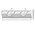
図2は、本発明の第1の実施形態に係る表示装置の概要を示す断面図である。表示装置は、表示パネル10を有する。本実施形態では、表示パネル10は、液晶表示パネルであって、一対の基板12,14(ガラス基板)を有し、両者間には図示しない液晶が介在する。基板12,14には、それぞれ、偏光板16が貼り付けられている。一方の基板12の周縁部には、液晶を駆動するためのドライバ回路を内蔵する集積回路チップ18が搭載され、フレキシブル配線基板20が取り付けられている。あるいは、表示パネル10は、有機EL(Electro Luminescence)パネルであってもよい。
FIG. 2 is a cross-sectional view showing an outline of the display device according to the first embodiment of the present invention. The display device has a
表示装置は、タッチパネル22(例えば静電容量結合方式のタッチパネル22)を有する。タッチパネル22と表示パネル10とは、粘着層24によって貼り付けられている。タッチパネル22が、画像を表示する表示パネル10に重ねられているので、画像に対して指による入力が可能になっている。タッチパネル22には、フレキシブル配線基板26が電気的に接続されている。
The display device includes a touch panel 22 (for example, a capacitively coupled touch panel 22). The
表示装置は、カバー基板28を有する。カバー基板28は、光透過性材料(例えばガラス)からなる。カバー基板28には、画像を表示する領域を囲むように遮光膜30が形成されている。遮光膜30が形成された面が、粘着層31を介して、タッチパネル22に貼り付けられている。
The display device has a
図3は、表示パネルの基板を示す図である。基板12は、画像表示領域32を有する。画像表示領域32には、複数の画素から画像が構成される。複数の画素は、図2にも示す集積回路チップ18に内蔵されるドライバ回路による駆動によって、明るさのレベルが変わるようになっている。駆動は走査方式で行うため、基板12には走査回路34が形成されている。例えば、矩形の画像表示領域32の対向する二辺の隣にそれぞれ走査回路34が形成され、他の一辺の隣に集積回路チップ18が搭載される。
FIG. 3 is a diagram illustrating a substrate of the display panel. The
図4は、画像を表示するための回路を示す図である。画像表示領域32には画素電極36が形成されている。複数の画素電極36によって画素が形成されるので、複数の画素電極36を囲む領域が画像表示領域32である。画像表示領域32には共通電極38が形成されている。共通電極38は基準電位(例えばGND)に設定され、画素電極36には、画素の明るさに応じた電圧が印加される。画素電極36と共通電極38の間に生じる電界を利用した光の制御(例えば液晶の駆動)で画像が表示される。
FIG. 4 is a diagram illustrating a circuit for displaying an image. A
共通電極38は、画像表示領域32の内側及び外側にわたって延びるコモン線40に電気的に接続している。画素電極36は、信号線42に電気的に接続されている。詳しくは、画素電極36と信号線42との間にスイッチング素子44(例えば薄膜トランジスタ)が接続されており、画素電極36と信号線42の電気的な導通及び遮断を行えるようになっている。スイッチング素子44は、走査回路34から引き出された走査線46に接続されており、走査線46に入力される走査信号によって駆動(オン/オフ)される。
The
信号線42は、画像表示領域32の内側にある内側信号線41と、画像表示領域32の外側にある外側信号線43からなる。内側信号線41が画素電極36に電気的に接続される。内側信号線41は、金属などの電気抵抗率が低い材料から形成されている。内側信号線41が共通電極38の近くを通るため、内側信号線41と共通電極38との間にカップリング容量Cが形成される。カップリング容量Cによって、基準電位に設定されるはずの共通電極38の電位が変動するが、本実施形態ではその変動を抑えるために次の特徴を有する。
The
図5は、外側信号線が形成された領域の詳細を示す図である。図6は、図5に示す領域のVI−VI線断面図である。図7は、図5に示す領域のVII−VII線断面図である。 FIG. 5 is a diagram showing details of a region where the outer signal line is formed. FIG. 6 is a cross-sectional view taken along the line VI-VI in the region shown in FIG. 7 is a cross-sectional view taken along the line VII-VII in the region shown in FIG.
外側信号線43は、第1部分48と第2部分50とを含む。第1部分48は、金属などの電気抵抗率が低い材料から形成されており、その材料は内側信号線41と同じ材料であってもよい。第2部分50は、第1部分48よりも電気抵抗が高く、例えば電気抵抗率の高い材料(例えば半導体材料)からなる。また、第2部分50は、図4に示す内側信号線41よりも電気抵抗率の高い材料から形成されている。図5の例では、内側信号線41に近い側に第2部分50が位置し、内側信号線41から離れた側に第1部分48が位置しているが、逆であってもよいし、一対の第1部分48の間に第2部分50があってもよいし、一対の第2部分50の間に第1部分48があってもよい。本実施形態では、第1部分48は、図3に示すように、集積回路チップ18に内蔵されるドライバ回路に電気的に接続される。
The
外側信号線43(第2部分50)が形成された領域では、図6及び図7に示すように、基板12には複数の膜が積層されている。複数の膜は、半導体膜52(例えばポリシリコン膜)を含む。半導体膜52は、図示しない位置で、薄膜トランジスタ(図4に示すスイッチング素子44)の一部を構成する。半導体膜52はゲート絶縁膜54で覆われており、薄膜トランジスタは、ゲート絶縁膜54上にゲート電極(図示せず)を有する。ゲート絶縁膜54上には層間絶縁膜56が形成されている。本実施形態では、第2部分50(図5)は、半導体膜52から形成されている。具体的には、第2部分50は、ポリシリコンからなる。
In the region where the outer signal line 43 (second portion 50) is formed, a plurality of films are laminated on the
本実施形態によれば、第2部分50は、第1部分48よりも電気抵抗が高い。つまり、外側信号線43の一部の電気抵抗が高くなっている。したがって、内側信号線41に伝達される信号は、外側信号線43を通るときに第2部分50の電気抵抗の高さによって遅延する。信号の遅延により、内側信号線41とのカップリング容量Cの影響を受ける共通電極38の電位変動のピークレベルを下げる。これにより、基準電位に設定される共通電極38の電位変動を抑えることができる。
According to the present embodiment, the
第2部分50(半導体膜52)は、絶縁膜(ゲート絶縁膜54及び層間絶縁膜56)に覆われている。絶縁膜(ゲート絶縁膜54及び層間絶縁膜56)には、第2部分50(半導体膜52)を露出する複数のコンタクトホール58が、第2部分50の長さ方向(図5参照)に間隔をあけて形成されている。コンタクトホール58を介して第2部分50との電気的な接続が可能になっている。第2部分50の長さ方向に離れた2つのコンタクトホール58を介して、第2部分50の離れた2個所を電気的に接続すれば、その離れた2個所間の電気抵抗を下げることができる。なお、図5の例では、第2部分50の幅方向に2つのコンタクトホール58が並んでいるが、これは第2部分50との電気的な接続を確実にするためのものである。
The second portion 50 (semiconductor film 52) is covered with an insulating film (
本実施形態では、第2部分50の離れた2個所の電気的接続はなされていないが、それぞれのコンタクトホール58で第2部分50に電気的に接続するように、絶縁膜(層間絶縁膜56)の上からコンタクトホール58内にわたって導電層60が形成されている。つまり、第2部分50の絶縁膜からの露出部がそれぞれ導電層60によって電気的に接続されている。導電層60は、第2部分50の材料よりも電気抵抗率の低い材料(例えば金属)からなる。そして、導電層60の形状を変更するだけで、第2部分50の離れた2個所の電気的接続が可能になる。詳しくは以下の変形例で説明する。導電層60の上には、無機パッシベーション膜62、有機パッシベーション膜64及び他の無機パッシベーション膜66が順に積層されている。
In the present embodiment, electrical connection is not made at two locations apart from the
[変形例]
図8は、図5に示す実施形態の変形例1を示す図である。図9は、図8に示す領域のIX−IX線断面図である。この例では、絶縁膜の上に導電層160が形成されている。導電層160は、第2部分150の長さ方向に離れた2つ以上のコンタクトホール158を通るように形成されている。導電層160はコンタクトホール158で第2部分150に電気的に接続する。つまり、第2部分150の長さ方向に離れた2つ以上のコンタクトホール158で、第2部分150の長さ方向に離れた個所が導電層160によって電気的に接続されている。導電層160は、第2部分150よりも電気抵抗が低いので、導電層160によって、第2部分150の離れた2個所の間の電気抵抗を下げることができる。電気抵抗を下げることで、第2部分150の電気抵抗の高さによる信号の遅延の程度を調整することができる。
[Modification]
FIG. 8 is a diagram illustrating a first modification of the embodiment illustrated in FIG. 5. 9 is a cross-sectional view of the region shown in FIG. 8 taken along the line IX-IX. In this example, a
導電層160は、第2部分150の任意の長さ離れた個所を電気的に接続することができ、任意の数のコンタクトホール158で第2部分150と電気的に接続することができる。例えば、図8には、第2部分150の長さ方向に第1距離d1を以て離れた2つのコンタクトホール158で第2部分150と電気的に接続する導電層160aと、他の第2部分150の長さ方向に第2距離d2を以て離れた一対のコンタクトホール158及びその間に位置する1つのコンタクトホール158で第2部分150と電気的に接続する導電層160bと、さらに他の第2部分150の長さ方向に第3距離d3を以て離れた一対のコンタクトホール158及びその間に位置する複数(2つ)のコンタクトホール158で第2部分150と電気的に接続する導電層160cと、が示されている。
The
図10は、図5に示す実施形態の変形例2を示す図である。この例では、いずれかのコンタクトホール258で第2部分250に接触するように絶縁膜の上に放熱層268が形成されている。放熱層268は、大きいほど放熱性が高くなる。放熱層268は、第2部分250の材料よりも熱伝導率が高い材料からなる。放熱層268が導電層であってもよい。
FIG. 10 is a diagram illustrating a second modification of the embodiment illustrated in FIG. 5. In this example, a heat dissipation layer 268 is formed on the insulating film so as to be in contact with the
図11は、図5に示す実施形態の変形例3を示す図である。図5に示す例では第2部分50は屈曲部を有することで長くなって全体的な電気抵抗を高くしてあるが、図11に示す例では第2部分350は直線を描くように真っ直ぐに延びているので比較的電気抵抗は低くなる。
FIG. 11 is a diagram illustrating a third modification of the embodiment illustrated in FIG. 5. In the example shown in FIG. 5, the
図12は、図5に示す実施形態の変形例4を示す図である。図5に示す例では第2部分50は互い違いに凸部を形成するように屈曲しているが、図12に示す例では第2部分450は、同じ方向に凸部を形成するように屈曲している。
FIG. 12 is a diagram illustrating a fourth modification of the embodiment illustrated in FIG. 5. In the example shown in FIG. 5, the
図13は、図5に示す実施形態の変形例5を示す図である。図5に示す第2部分50では、第2部分50の長さ方向に離れた一対のコンタクトホール58の間で1つの凸部が形成されるように屈曲するのに対して、図13に示す第2部分550では、第2部分550の長さ方向に離れた一対のコンタクトホール558の間で複数(例えば2つ)の凸部が形成されるように屈曲する。複数の凸部は、図13に示すように相互に反対方向に突出するように形成されてもよいし、同じ方向に突出するように形成されていてもよい。
FIG. 13 is a diagram illustrating a fifth modification of the embodiment illustrated in FIG. 5. The
図14は、図5に示す実施形態の変形例6を示す図である。この例では、第2部分650は、第2部分650の長さ方向に離れた一対のコンタクトホール658の間で、クランク状に屈曲している。
FIG. 14 is a diagram illustrating a sixth modification of the embodiment illustrated in FIG. 5. In this example, the
[第2の実施形態]
図15は、本発明の第2の実施形態に係る表示装置が有する表示パネルの基板を示す図である。図16は、画像を表示するための回路を示す図である。
[Second Embodiment]
FIG. 15 is a diagram showing a substrate of a display panel included in the display device according to the second embodiment of the present invention. FIG. 16 is a diagram illustrating a circuit for displaying an image.
表示装置は、画像表示領域732を有する基板712を有する。画像表示領域732の内側に内側信号線741が形成され、画像表示領域732の外側に外側信号線743が形成されている。画像表示領域732の内側及び外側を通るようにコモン線740が形成されている。
The display device includes a
本実施形態に係る表示装置は、図4に示す第1の実施形態で説明した画素電極36と共通電極38を有し、画素電極36と共通電極38の間に生じる電界を利用した光の制御で画像を表示する。その詳細は上記第1の実施形態で説明した通りであり、内側信号線41と共通電極38との間にカップリング容量Cが形成される点も共通である。
The display device according to the present embodiment includes the
図16に示すように、本実施形態に係る表示装置は、RGB選択回路772を有する点で第1の実施形態と相違する。RGB選択回路772によって、外側信号線743の数を減らすことができる。
As shown in FIG. 16, the display device according to the present embodiment is different from the first embodiment in that it includes an
詳しくは、RGB選択回路772は、m(図16ではm=6)個のスイッチング素子744を有する。スイッチング素子744は、内側信号線741と外側信号線743との電気的な導通及び遮断を切り替える。スイッチング素子744には、制御線770から制御信号が入力される。制御線770に制御信号が入力されることで、スイッチング素子744が外側信号線743と内側信号線741を接続する。
Specifically, the
制御線770の数は、n(図16ではn=3)本である。m個のスイッチング素子744は、制御線770と同じ数のn個ごとにグループ化されている。各グループのn個のスイッチング素子744は、それぞれ異なる制御線770で制御される。m個のスイッチング素子744のそれぞれに、m本の内側信号線741の1本が電気的に接続される。各グループのn個のスイッチング素子744に電気的に接続するように、(m/n)本の外側信号線743のそれぞれ(1本)は、n本に分岐している。n本の制御線770の1つに制御信号が入力されることで、各グループの1つのスイッチング素子744が、1本の外側信号線743と1本の内側信号線741を接続する。
The number of
1本の走査線(図示せず)に沿って並ぶ複数の画素は、赤色の画素R1,R2,…、緑色の画素G1,G2,…、青色の画素B1,B2,…を有する。制御線770は、RGB選択回路772に接続されており、いずれかの色を選択するようになっている。そのため、画素の色の数(RGBの3色)と制御線770の数が同じになっている。制御線770によって、いずれかの色が選択されると、その色の画素に、信号線742(外側信号線743)から信号が入力される。
A plurality of pixels arranged along one scanning line (not shown) are red pixels R 1 , R 2 ,..., Green pixels G 1 , G 2 ,..., Blue pixels B 1 , B 2 ,. Has ... The
例えば、赤の画素R1,R2が選択されると制御線770Rに制御信号が入力され、スイッチング素子744R1及びスイッチング素子744R2がオンになって、外側信号線743aと内側信号線741R1を接続し、外側信号線743bと内側信号線741R2を接続する。このとき、外側信号線743a及び外側信号線743bには、それぞれ、赤の画素R1,R2に対応した信号が入力されており、信号に応じて赤の画素R1,R2が表示される。
For example, when the red pixels R 1 and R 2 are selected, a control signal is input to the
緑の画素G1,G2が選択されると制御線770Gに制御信号が入力され、スイッチング素子744G1及びスイッチング素子744G2がオンになって、外側信号線743aと内側信号線741G2を接続し、外側信号線743bと内側信号線741G1を接続する。このとき、外側信号線743a及び外側信号線743bには、それぞれ、緑の画素G1,G2に対応した信号が入力されており、信号に応じて緑の画素G1,G2が表示される。
When the green pixels G 1 and G 2 are selected, a control signal is input to the
青の画素B1,B2が選択されると制御線770Bに制御信号が入力され、スイッチング素子744B1及びスイッチング素子744B2がオンになって、外側信号線743aと内側信号線741B1を接続し、外側信号線743bと内側信号線741B2を接続する。このとき、外側信号線743a及び外側信号線743bには、それぞれ、青の画素B1,B2に対応した信号が入力されており、信号に応じて青の画素B1,B2が表示される。
When the blue pixels B 1 and B 2 are selected, a control signal is input to the
図17は、制御線770を示す図である。制御線770は、第1部分748と第2部分750とを含む。第1部分748は、金属などの電気抵抗率が低い材料から形成されており、その材料は内側信号線741と同じ材料であってもよい。第2部分750は、第1部分748よりも電気抵抗が高い。この例では、第2部分750は、第1部分748よりも細く(幅が狭くなるように)形成されることで、電気抵抗を高くしてある。したがって、第2部分750は、第1部分748と同じ材料(例えば金属)で形成されている。このことは、第1の実施形態にも適用可能である。逆に、第1の実施形態で説明したように、第2部分750を、第1部分748又は内側信号線741よりも電気抵抗率の高い材料(例えばポリシリコンなどの半導体材料)から形成してもよい。
FIG. 17 is a diagram illustrating the
本実施形態によれば、スイッチング素子744に入力される制御信号は、制御線770を通るときに第2部分750の電気抵抗の高さによって遅延する。制御信号の遅延より、スイッチング素子744の動作が遅くなるので、内側信号線741に伝達される信号が遅延する。これにより、内側信号線741とのカップリング容量の影響を受ける共通電極(図示せず)の電位変動のピークレベルが下がるので、基準電位に設定される共通電極(図示せず)の電位変動を抑えることができる。
According to the present embodiment, the control signal input to the
[変形例]
図18は、第2の実施形態の変形例1を示す図である。この例では、第2部分850に電気的に接続するように導電層860が形成されている。詳しくは、第2部分850が金属で形成されていても細くなっていることで電気抵抗が高いが、第2部分850の長さ方向に離れた2つ以上のコンタクトホール858で、第2部分850の長さ方向に離れた個所が導電層860によって電気的に接続されている。導電層860は第2部分850よりも幅が広いので電気抵抗が低くなる。そのため、導電層860によって、第2部分850の離れた2個所の間の電気抵抗を下げることができる。電気抵抗を下げることで、第2部分850の電気抵抗の高さによる信号の遅延の程度を調整することができる。
[Modification]
FIG. 18 is a diagram illustrating a first modification of the second embodiment. In this example, a
図19は、第2の実施形態の変形例2を示す図である。この例でも、導電層960は、第2部分950の任意の長さ離れた個所を電気的に接続することができ、任意の数のコンタクトホール958で第2部分950と電気的に接続することができる。例えば、図19には、第2部分950の長さ方向に第1距離d11を以て離れた2つのコンタクトホール958で第2部分950と電気的に接続する導電層960aと、他の第2部分950の長さ方向に第2距離d22を以て離れた一対のコンタクトホール958及びその間に位置する1つのコンタクトホール958で第2部分950と電気的に接続する導電層960bと、さらに他の第2部分950の長さ方向に第3距離d33を以て離れた一対のコンタクトホール958及びその間に位置する複数(2つ)のコンタクトホール958で第2部分950と電気的に接続する導電層960cと、が示されている。
FIG. 19 is a diagram illustrating a second modification of the second embodiment. Also in this example, the
本発明は、上述した実施形態に限定されるものではなく種々の変形が可能である。例えば、実施形態で説明した構成は、実質的に同一の構成、同一の作用効果を奏する構成又は同一の目的を達成することができる構成で置き換えることができる。 The present invention is not limited to the above-described embodiments, and various modifications can be made. For example, the configuration described in the embodiment can be replaced with substantially the same configuration, a configuration that exhibits the same operational effects, or a configuration that can achieve the same purpose.
10 表示パネル、12 基板、14 基板、16 偏光板、18 集積回路チップ、20 フレキシブル配線基板、22 タッチパネル、24 粘着層、26 フレキシブル配線基板、28 カバー基板、30 遮光膜、32 画像表示領域、34 走査回路、36 画素電極、38 共通電極、40 コモン線、41 内側信号線、42 信号線、43 外側信号線、44 スイッチング素子、46 走査線、48 第1部分、50 第2部分、52 半導体膜、54 ゲート絶縁膜、56 層間絶縁膜、58 コンタクトホール、60 導電層、62 無機パッシベーション膜、64 有機パッシベーション膜、66 無機パッシベーション膜、150 第2部分、158 コンタクトホール、160 導電層、250 第2部分、258 コンタクトホール、268 放熱層、350 第2部分、450 第2部分、550 第2部分、558 コンタクトホール、650 第2部分、658 コンタクトホール、712 基板、732 画像表示領域、740 コモン線、741 内側信号線、742 信号線、743 外側信号線、744 スイッチング素子、748 第1部分、750 第2部分、770 制御線、772 RGB選択回路、850 第2部分、858 コンタクトホール、860 導電層、950 第2部分、958 コンタクトホール、960 導電層。 DESCRIPTION OF SYMBOLS 10 Display panel, 12 board | substrate, 14 board | substrate, 16 polarizing plate, 18 integrated circuit chip, 20 flexible wiring board, 22 touch panel, 24 adhesive layer, 26 flexible wiring board, 28 cover board | substrate, 30 light shielding film, 32 image display area, 34 Scanning circuit, 36 pixel electrode, 38 common electrode, 40 common line, 41 inner signal line, 42 signal line, 43 outer signal line, 44 switching element, 46 scanning line, 48 first part, 50 second part, 52 semiconductor film 54 gate insulating film, 56 interlayer insulating film, 58 contact hole, 60 conductive layer, 62 inorganic passivation film, 64 organic passivation film, 66 inorganic passivation film, 150 second part, 158 contact hole, 160 conductive layer, 250 second Part, 258 contact hole, 68 Heat dissipation layer, 350 Second part, 450 Second part, 550 Second part, 558 Contact hole, 650 Second part, 658 Contact hole, 712 Substrate, 732 Image display area, 740 Common line, 741 Inside signal line, 742 Signal line, 743 Outside signal line, 744 switching element, 748 first part, 750 second part, 770 control line, 772 RGB selection circuit, 850 second part, 858 contact hole, 860 conductive layer, 950 second part, 958 Contact hole, 960 conductive layer.
Claims (9)
前記基板の前記画像表示領域に形成された画素電極と、
前記基板の前記画像表示領域に形成された共通電極と、
前記基板の前記画像表示領域の内側に形成されて前記画素電極に電気的に接続される複数の内側信号線と、
前記基板の前記画像表示領域の外側に形成されて前記複数の内側信号線にそれぞれ電気的に接続される複数の外側信号線と、
前記基板の前記画像表示領域の内側及び外側に形成されて前記共通電極に電気的に接続されるコモン線と、
複数の導電層と、
を有し、
前記画素電極と前記共通電極の間に生じる電界を利用した光の制御で画像を表示し、
前記複数の内側信号線と前記共通電極との間にカップリング容量が形成され、
前記複数の外側信号線のそれぞれ及び前記複数の内側信号線のそれぞれの少なくとも一方は、第1部分と、前記第1部分よりも電気抵抗が高い第2部分と、を含み、
前記第2部分を覆うように絶縁膜が設けられ、
前記絶縁膜には、前記第2部分を露出する複数のコンタクトホールが、前記第2部分の長さ方向に間隔をあけて形成され、
2つ以上の前記コンタクトホールで前記第2部分に電気的に接続するように前記絶縁膜の上に前記複数の導電層のそれぞれが形成され、
前記複数の導電層は、それぞれ、前記第2部分の材料とは電気抵抗が異なり、前記第2部分の長さ方向に沿った長さが相互に異なることを特徴とする表示装置。 A substrate having an image display area;
A pixel electrode formed in the image display area of the substrate;
A common electrode formed in the image display region of the substrate;
A plurality of inner signal lines formed inside the image display area of the substrate and electrically connected to the pixel electrodes;
A plurality of outer signal lines electrically connected to the plurality of inner signal lines formed outside of the image display area of the substrate,
A common line formed inside and outside the image display area of the substrate and electrically connected to the common electrode;
A plurality of conductive layers;
Have
An image is displayed by controlling light using an electric field generated between the pixel electrode and the common electrode,
A coupling capacitor is formed between the plurality of inner signal lines and the common electrode;
At least one of each of the plurality of outer signal lines and each of the plurality of inner signal lines includes a first portion and a second portion having a higher electrical resistance than the first portion,
An insulating film is provided to cover the second portion;
In the insulating film, a plurality of contact holes exposing the second part are formed at intervals in the length direction of the second part,
Each of the plurality of conductive layers is formed on the insulating film so as to be electrically connected to the second portion through two or more contact holes,
Wherein the plurality of conductive layers, respectively, wherein the second portion of the material Ri Do different electrical resistance, a display device whose length along the length direction of the second portion, characterized in Rukoto different from each other.
前記基板の前記画像表示領域に形成された画素電極と、
前記基板の前記画像表示領域に形成された共通電極と、
前記基板の前記画像表示領域の内側に形成されて前記画素電極に電気的に接続される内側信号線と、
前記基板の前記画像表示領域の外側に形成される外側信号線と、
前記内側信号線と前記外側信号線との間で電気的な導通及び遮断を切り替えるスイッチング素子と、
前記スイッチング素子に制御信号を入力するための制御線と、
前記基板の前記画像表示領域の内側及び外側に形成されて前記共通電極に電気的に接続されるコモン線と、
を有し、
前記画素電極と前記共通電極の間に生じる電界を利用した光の制御で画像を表示し、
前記内側信号線と前記共通電極との間にカップリング容量が形成され、
前記制御線は、第1部分と、前記第1部分よりも電気抵抗が高い第2部分と、を含み、
前記第2部分を覆うように絶縁膜が設けられ、
前記絶縁膜には、前記第2部分を露出する複数のコンタクトホールが、前記第2部分の長さ方向に間隔をあけて形成され、
前記第2部分は、屈曲部を有し、
前記屈曲部を間に挟む2つ以上の前記コンタクトホールで前記第2部分に電気的に接続するように前記絶縁膜の上に導電層が形成され、
前記導電層は、前記第2部分の材料とは電気抵抗が異なり、前記第2部分の前記屈曲部と重ならない部分を有することを特徴とする表示装置。 A substrate having an image display area;
A pixel electrode formed in the image display area of the substrate;
A common electrode formed in the image display region of the substrate;
An inner signal line formed inside the image display area of the substrate and electrically connected to the pixel electrode;
An outer signal line formed outside the image display area of the substrate;
A switching element that switches between electrical conduction and interruption between the inner signal line and the outer signal line;
A control line for inputting a control signal to the switching element;
A common line formed inside and outside the image display area of the substrate and electrically connected to the common electrode;
Have
An image is displayed by controlling light using an electric field generated between the pixel electrode and the common electrode,
A coupling capacitor is formed between the inner signal line and the common electrode;
The control line includes a first portion and a second portion having a higher electrical resistance than the first portion,
An insulating film is provided to cover the second portion;
In the insulating film, a plurality of contact holes exposing the second part are formed at intervals in the length direction of the second part,
The second portion has a bent portion;
A conductive layer is formed on the insulating film so as to be electrically connected to the second portion through the two or more contact holes sandwiching the bent portion ;
The conductive layer, the Ri electrical resistance Do different from the second portion of the material, the display device according to claim Rukoto that having a said do not overlap with the bent portion of the second portion.
n本の前記制御線と、
前記制御線と同じ数のn個ごとにグループ化され、各グループではそれぞれ異なる前記制御線で制御されるm個の前記スイッチング素子と、
m個の前記スイッチング素子のそれぞれに1本が電気的に接続されるm本の前記内側信号線と、
各グループのn個の前記スイッチング素子に1本から分岐して電気的に接続する(m/n)本の前記外側信号線と、
を有し、
n本の前記制御線の1つに制御信号が入力されることで、各グループの1つの前記スイッチング素子が、1本の前記外側信号線と1本の前記内側信号線を接続することを特徴とする表示装置。 The display device according to claim 2,
n control lines;
M switching elements that are grouped by the same number n as the control lines, and are controlled by the control lines that are different in each group;
m inner signal lines, one of which is electrically connected to each of the m switching elements,
(M / n) outer signal lines branched from one to n switching elements of each group and electrically connected;
Have
A control signal is input to one of the n control lines, so that one switching element of each group connects one outer signal line and one inner signal line. Display device.
前記導電層は、前記第2部分の材料よりも電気抵抗率の低い材料からなることを特徴とする表示装置。 The display device according to any one of claims 1 to 3,
The display device, wherein the conductive layer is made of a material having an electric resistivity lower than that of the material of the second portion.
前記導電層は、放熱層であり、前記第2部分の材料よりも熱伝導率が高い材料からなることを特徴とする表示装置。 The display device according to any one of claims 1 to 3,
The display device, wherein the conductive layer is a heat dissipation layer and is made of a material having a higher thermal conductivity than the material of the second portion.
前記第2部分は、ポリシリコンからなることを特徴とする表示装置。 The display device according to any one of claims 1 to 5,
The display device, wherein the second portion is made of polysilicon.
前記第2部分は、直線を描くように延びることを特徴とする表示装置。 The display device according to claim 1 ,
The display device, wherein the second portion extends to draw a straight line.
前記複数のコンタクトホールは、最も離れた一対の第1コンタクトホールと、前記一対の第1コンタクトホールに挟まれた位置にある第2コンタクトホールと、を含み、
前記複数の導電層のいずれかは、少なくとも前記一対の第1コンタクトホールで前記第2部分に電気的に接続することを特徴とする表示装置。 The display device according to claim 1 ,
The plurality of contact holes include a pair of first contact holes that are farthest apart and a second contact hole that is located between the pair of first contact holes,
One of the plurality of conductive layers is electrically connected to the second portion through at least the pair of first contact holes .
前記基板と重ねられたタッチパネルをさらに有することを特徴とする表示装置。 The display device according to any one of claims 1 to 8,
The display device further comprising a touch panel overlaid on the substrate.
Priority Applications (10)
| Application Number | Priority Date | Filing Date | Title |
|---|---|---|---|
| JP2012097266A JP6022805B2 (en) | 2012-04-23 | 2012-04-23 | Display device |
| US13/851,130 US8878815B2 (en) | 2012-04-23 | 2013-03-27 | Display device |
| CN201610113361.6A CN105573560B (en) | 2012-04-23 | 2013-03-28 | Display device |
| CN201310116617.5A CN103376605B (en) | 2012-04-23 | 2013-03-28 | Display device |
| US14/526,807 US9214115B2 (en) | 2012-04-23 | 2014-10-29 | Display device |
| US14/938,039 US9437143B2 (en) | 2012-04-23 | 2015-11-11 | Display device |
| US15/227,015 US9704447B2 (en) | 2012-04-23 | 2016-08-03 | Display device |
| US15/497,286 US9928792B2 (en) | 2012-04-23 | 2017-04-26 | Display device |
| US15/898,272 US10134351B2 (en) | 2012-04-23 | 2018-02-16 | Display device |
| US16/161,909 US10593276B2 (en) | 2012-04-23 | 2018-10-16 | Display device |
Applications Claiming Priority (1)
| Application Number | Priority Date | Filing Date | Title |
|---|---|---|---|
| JP2012097266A JP6022805B2 (en) | 2012-04-23 | 2012-04-23 | Display device |
Publications (3)
| Publication Number | Publication Date |
|---|---|
| JP2013225032A JP2013225032A (en) | 2013-10-31 |
| JP2013225032A5 JP2013225032A5 (en) | 2015-06-11 |
| JP6022805B2 true JP6022805B2 (en) | 2016-11-09 |
Family
ID=49379652
Family Applications (1)
| Application Number | Title | Priority Date | Filing Date |
|---|---|---|---|
| JP2012097266A Active JP6022805B2 (en) | 2012-04-23 | 2012-04-23 | Display device |
Country Status (3)
| Country | Link |
|---|---|
| US (7) | US8878815B2 (en) |
| JP (1) | JP6022805B2 (en) |
| CN (2) | CN105573560B (en) |
Families Citing this family (19)
| Publication number | Priority date | Publication date | Assignee | Title |
|---|---|---|---|---|
| JP6022805B2 (en) * | 2012-04-23 | 2016-11-09 | 株式会社ジャパンディスプレイ | Display device |
| USD725650S1 (en) | 2012-12-06 | 2015-03-31 | Intel Corporation | Computing device |
| USD738370S1 (en) * | 2013-07-04 | 2015-09-08 | Lg Electronics Inc. | Tablet PC |
| TWD161239S (en) * | 2013-07-04 | 2014-06-21 | Lg電子股份有限公司 | Tablet pc |
| USD761786S1 (en) * | 2013-08-21 | 2016-07-19 | Intel Corporation | Electronic device |
| USD754123S1 (en) | 2013-08-21 | 2016-04-19 | Intel Corporation | Electronic device |
| USD746281S1 (en) * | 2014-02-03 | 2015-12-29 | Lg Electronics Inc. | Tablet computer |
| USD840392S1 (en) | 2014-12-27 | 2019-02-12 | Intel Corporation | Computing device |
| US10134511B2 (en) | 2015-03-26 | 2018-11-20 | Seiko Epson Corporation | Resistance element, electrostatic protection circuit, temperature detection circuit, and electro-optic apparatus |
| TWI567603B (en) * | 2015-04-16 | 2017-01-21 | Au Optronics Corp | Touch display device |
| KR102369089B1 (en) * | 2015-04-17 | 2022-03-02 | 삼성디스플레이 주식회사 | Flexible display device |
| KR102433650B1 (en) | 2015-10-29 | 2022-08-19 | 삼성디스플레이 주식회사 | Display device |
| CN105867035A (en) * | 2016-06-12 | 2016-08-17 | 武汉华星光电技术有限公司 | Fan-out routing system, array substrate and liquid crystal display device |
| KR102601650B1 (en) * | 2016-07-26 | 2023-11-13 | 삼성디스플레이 주식회사 | Display device |
| CN107634072B (en) * | 2017-10-25 | 2020-04-03 | 厦门天马微电子有限公司 | Array substrate and display panel |
| CN111383608B (en) * | 2018-12-29 | 2022-01-25 | 北京小米移动软件有限公司 | Display control method and apparatus, electronic device, and computer-readable storage medium |
| CN110362227B (en) * | 2019-06-25 | 2021-01-01 | 武汉华星光电半导体显示技术有限公司 | Touch panel and touch display device |
| CN111755465B (en) * | 2020-06-30 | 2022-09-23 | 厦门天马微电子有限公司 | Display module and display device |
| CN116400538A (en) * | 2023-03-14 | 2023-07-07 | 惠科股份有限公司 | Array substrate, display panel and display device |
Family Cites Families (22)
| Publication number | Priority date | Publication date | Assignee | Title |
|---|---|---|---|---|
| KR100237679B1 (en) * | 1995-12-30 | 2000-01-15 | 윤종용 | Liquid crystal display panel |
| KR100697903B1 (en) * | 1997-04-11 | 2007-03-20 | 가부시키가이샤 히타치세이사쿠쇼 | Liquid crystal display device |
| JP4206518B2 (en) * | 1998-08-03 | 2009-01-14 | セイコーエプソン株式会社 | Electro-optical device, manufacturing method thereof, and electronic apparatus |
| JP3669282B2 (en) * | 2000-05-19 | 2005-07-06 | セイコーエプソン株式会社 | Electro-optical device and electronic apparatus |
| JP2003140181A (en) * | 2001-11-02 | 2003-05-14 | Nec Corp | Liquid crystal display device |
| JP4015908B2 (en) * | 2002-08-29 | 2007-11-28 | 松下電器産業株式会社 | Display device drive circuit and display device |
| JP4199501B2 (en) * | 2002-09-13 | 2008-12-17 | Nec液晶テクノロジー株式会社 | Manufacturing method of liquid crystal display device |
| JP3980462B2 (en) * | 2002-10-30 | 2007-09-26 | 株式会社 日立ディスプレイズ | Image display device |
| US7271784B2 (en) * | 2002-12-18 | 2007-09-18 | Semiconductor Energy Laboratory Co., Ltd. | Display device and driving method thereof |
| JP4487875B2 (en) * | 2005-07-20 | 2010-06-23 | セイコーエプソン株式会社 | Method for manufacturing electronic substrate, method for manufacturing electro-optical device, and method for manufacturing electronic device |
| CN100388101C (en) * | 2005-10-12 | 2008-05-14 | 友达光电股份有限公司 | Fan type wire structure |
| CN100538804C (en) * | 2005-10-21 | 2009-09-09 | 友达光电股份有限公司 | Display panel |
| JP2007133067A (en) * | 2005-11-09 | 2007-05-31 | Epson Imaging Devices Corp | Method of manufacturing electrooptical device |
| KR101392160B1 (en) * | 2006-08-25 | 2014-05-08 | 삼성디스플레이 주식회사 | Liquid crystal display device |
| JP5413937B2 (en) | 2006-09-28 | 2014-02-12 | 株式会社ジャパンディスプレイ | Electro-optical device and electronic apparatus |
| JP2008250223A (en) * | 2007-03-30 | 2008-10-16 | Casio Comput Co Ltd | Liquid crystal display device |
| JP5067690B2 (en) * | 2007-05-18 | 2012-11-07 | Nltテクノロジー株式会社 | Liquid crystal display device and terminal device |
| JP4448535B2 (en) * | 2007-12-18 | 2010-04-14 | 株式会社 日立ディスプレイズ | Display device |
| JP2010054551A (en) * | 2008-08-26 | 2010-03-11 | Epson Imaging Devices Corp | Display device and inspection probe for the display device |
| JP5463658B2 (en) * | 2008-12-03 | 2014-04-09 | セイコーエプソン株式会社 | Electro-optical device and electronic apparatus |
| JP5348473B2 (en) * | 2009-01-20 | 2013-11-20 | ソニー株式会社 | Liquid crystal display device and electronic device |
| JP6022805B2 (en) * | 2012-04-23 | 2016-11-09 | 株式会社ジャパンディスプレイ | Display device |
-
2012
- 2012-04-23 JP JP2012097266A patent/JP6022805B2/en active Active
-
2013
- 2013-03-27 US US13/851,130 patent/US8878815B2/en active Active
- 2013-03-28 CN CN201610113361.6A patent/CN105573560B/en active Active
- 2013-03-28 CN CN201310116617.5A patent/CN103376605B/en active Active
-
2014
- 2014-10-29 US US14/526,807 patent/US9214115B2/en active Active
-
2015
- 2015-11-11 US US14/938,039 patent/US9437143B2/en active Active
-
2016
- 2016-08-03 US US15/227,015 patent/US9704447B2/en active Active
-
2017
- 2017-04-26 US US15/497,286 patent/US9928792B2/en active Active
-
2018
- 2018-02-16 US US15/898,272 patent/US10134351B2/en active Active
- 2018-10-16 US US16/161,909 patent/US10593276B2/en active Active
Also Published As
| Publication number | Publication date |
|---|---|
| US20150054804A1 (en) | 2015-02-26 |
| US10134351B2 (en) | 2018-11-20 |
| US9928792B2 (en) | 2018-03-27 |
| US9437143B2 (en) | 2016-09-06 |
| US20160343327A1 (en) | 2016-11-24 |
| US9704447B2 (en) | 2017-07-11 |
| CN105573560B (en) | 2018-10-19 |
| JP2013225032A (en) | 2013-10-31 |
| CN105573560A (en) | 2016-05-11 |
| CN103376605B (en) | 2016-03-30 |
| US20130278553A1 (en) | 2013-10-24 |
| CN103376605A (en) | 2013-10-30 |
| US20160063931A1 (en) | 2016-03-03 |
| US9214115B2 (en) | 2015-12-15 |
| US10593276B2 (en) | 2020-03-17 |
| US20180174539A1 (en) | 2018-06-21 |
| US8878815B2 (en) | 2014-11-04 |
| US20190088225A1 (en) | 2019-03-21 |
| US20170229080A1 (en) | 2017-08-10 |
Similar Documents
| Publication | Publication Date | Title |
|---|---|---|
| JP6022805B2 (en) | Display device | |
| US20200159357A1 (en) | Display device and liquid crystal display device with built-in touch panel | |
| JP6131071B2 (en) | Touch panel built-in display device | |
| TWI510988B (en) | In-cell touch display panel | |
| JP5806383B2 (en) | Liquid crystal display | |
| JP2016038697A (en) | Sensor device and display device | |
| JP5934382B2 (en) | Display device | |
| JP2014145919A (en) | Display device | |
| JP6410908B2 (en) | LCD with built-in touch panel | |
| JP6240278B2 (en) | LCD with built-in touch panel | |
| JP2014123273A (en) | Input device, and display device including the same | |
| JP2014186409A (en) | Display device | |
| JP2012093610A (en) | Liquid crystal display device |
Legal Events
| Date | Code | Title | Description |
|---|---|---|---|
| A521 | Request for written amendment filed |
Free format text: JAPANESE INTERMEDIATE CODE: A523 Effective date: 20150417 |
|
| A621 | Written request for application examination |
Free format text: JAPANESE INTERMEDIATE CODE: A621 Effective date: 20150417 |
|
| A977 | Report on retrieval |
Free format text: JAPANESE INTERMEDIATE CODE: A971007 Effective date: 20160224 |
|
| A131 | Notification of reasons for refusal |
Free format text: JAPANESE INTERMEDIATE CODE: A131 Effective date: 20160301 |
|
| A521 | Request for written amendment filed |
Free format text: JAPANESE INTERMEDIATE CODE: A523 Effective date: 20160406 |
|
| TRDD | Decision of grant or rejection written | ||
| A01 | Written decision to grant a patent or to grant a registration (utility model) |
Free format text: JAPANESE INTERMEDIATE CODE: A01 Effective date: 20160913 |
|
| A61 | First payment of annual fees (during grant procedure) |
Free format text: JAPANESE INTERMEDIATE CODE: A61 Effective date: 20161006 |
|
| R150 | Certificate of patent or registration of utility model |
Ref document number: 6022805 Country of ref document: JP Free format text: JAPANESE INTERMEDIATE CODE: R150 |
|
| R250 | Receipt of annual fees |
Free format text: JAPANESE INTERMEDIATE CODE: R250 |
|
| R250 | Receipt of annual fees |
Free format text: JAPANESE INTERMEDIATE CODE: R250 |
|
| R250 | Receipt of annual fees |
Free format text: JAPANESE INTERMEDIATE CODE: R250 |
|
| R250 | Receipt of annual fees |
Free format text: JAPANESE INTERMEDIATE CODE: R250 |
|
| R250 | Receipt of annual fees |
Free format text: JAPANESE INTERMEDIATE CODE: R250 |