JP3666411B2 - High frequency module device - Google Patents
High frequency module device Download PDFInfo
- Publication number
- JP3666411B2 JP3666411B2 JP2001136490A JP2001136490A JP3666411B2 JP 3666411 B2 JP3666411 B2 JP 3666411B2 JP 2001136490 A JP2001136490 A JP 2001136490A JP 2001136490 A JP2001136490 A JP 2001136490A JP 3666411 B2 JP3666411 B2 JP 3666411B2
- Authority
- JP
- Japan
- Prior art keywords
- wiring
- layer
- pattern
- frequency
- base substrate
- Prior art date
- Legal status (The legal status is an assumption and is not a legal conclusion. Google has not performed a legal analysis and makes no representation as to the accuracy of the status listed.)
- Expired - Lifetime
Links
- 239000000758 substrate Substances 0.000 claims description 70
- 239000004020 conductor Substances 0.000 claims description 22
- 239000011368 organic material Substances 0.000 claims description 12
- 230000015572 biosynthetic process Effects 0.000 claims description 7
- 239000010410 layer Substances 0.000 description 100
- 230000005540 biological transmission Effects 0.000 description 29
- 239000010408 film Substances 0.000 description 14
- 238000000034 method Methods 0.000 description 13
- 238000004891 communication Methods 0.000 description 12
- 239000010409 thin film Substances 0.000 description 11
- 239000000463 material Substances 0.000 description 9
- 239000010949 copper Substances 0.000 description 6
- 229920002120 photoresistant polymer Polymers 0.000 description 6
- RYGMFSIKBFXOCR-UHFFFAOYSA-N Copper Chemical compound [Cu] RYGMFSIKBFXOCR-UHFFFAOYSA-N 0.000 description 5
- 238000006243 chemical reaction Methods 0.000 description 5
- 239000004065 semiconductor Substances 0.000 description 5
- 229920000106 Liquid crystal polymer Polymers 0.000 description 4
- 239000004977 Liquid-crystal polymers (LCPs) Substances 0.000 description 4
- 239000003990 capacitor Substances 0.000 description 4
- 238000005516 engineering process Methods 0.000 description 4
- 238000007747 plating Methods 0.000 description 4
- 229920000636 poly(norbornene) polymer Polymers 0.000 description 4
- 229910052802 copper Inorganic materials 0.000 description 3
- 229910000365 copper sulfate Inorganic materials 0.000 description 3
- ARUVKPQLZAKDPS-UHFFFAOYSA-L copper(II) sulfate Chemical compound [Cu+2].[O-][S+2]([O-])([O-])[O-] ARUVKPQLZAKDPS-UHFFFAOYSA-L 0.000 description 3
- 230000008878 coupling Effects 0.000 description 3
- 238000010168 coupling process Methods 0.000 description 3
- 238000005859 coupling reaction Methods 0.000 description 3
- 238000009713 electroplating Methods 0.000 description 3
- 239000011521 glass Substances 0.000 description 3
- 238000000206 photolithography Methods 0.000 description 3
- 239000004642 Polyimide Substances 0.000 description 2
- 230000003321 amplification Effects 0.000 description 2
- 239000000919 ceramic Substances 0.000 description 2
- 239000011248 coating agent Substances 0.000 description 2
- 238000000576 coating method Methods 0.000 description 2
- 239000011889 copper foil Substances 0.000 description 2
- 238000005530 etching Methods 0.000 description 2
- 238000000605 extraction Methods 0.000 description 2
- 239000011229 interlayer Substances 0.000 description 2
- 238000003199 nucleic acid amplification method Methods 0.000 description 2
- 229920001721 polyimide Polymers 0.000 description 2
- -1 polyphenylethylene Polymers 0.000 description 2
- 239000011347 resin Substances 0.000 description 2
- 229920005989 resin Polymers 0.000 description 2
- 239000000126 substance Substances 0.000 description 2
- 238000010897 surface acoustic wave method Methods 0.000 description 2
- 238000004804 winding Methods 0.000 description 2
- VXNZUUAINFGPBY-UHFFFAOYSA-N 1-Butene Chemical compound CCC=C VXNZUUAINFGPBY-UHFFFAOYSA-N 0.000 description 1
- 239000004925 Acrylic resin Substances 0.000 description 1
- 229920000178 Acrylic resin Polymers 0.000 description 1
- 239000004593 Epoxy Substances 0.000 description 1
- 229910000577 Silicon-germanium Inorganic materials 0.000 description 1
- 239000004840 adhesive resin Substances 0.000 description 1
- 229920006223 adhesive resin Polymers 0.000 description 1
- IAQRGUVFOMOMEM-UHFFFAOYSA-N butene Natural products CC=CC IAQRGUVFOMOMEM-UHFFFAOYSA-N 0.000 description 1
- 238000007766 curtain coating Methods 0.000 description 1
- 238000001514 detection method Methods 0.000 description 1
- 238000003618 dip coating Methods 0.000 description 1
- 238000005553 drilling Methods 0.000 description 1
- 230000000694 effects Effects 0.000 description 1
- 239000003822 epoxy resin Substances 0.000 description 1
- 238000007667 floating Methods 0.000 description 1
- 230000004048 modification Effects 0.000 description 1
- 238000012986 modification Methods 0.000 description 1
- 238000004806 packaging method and process Methods 0.000 description 1
- 230000000149 penetrating effect Effects 0.000 description 1
- 238000005498 polishing Methods 0.000 description 1
- 229920000647 polyepoxide Polymers 0.000 description 1
- 229920001343 polytetrafluoroethylene Polymers 0.000 description 1
- 239000004810 polytetrafluoroethylene Substances 0.000 description 1
- 238000004528 spin coating Methods 0.000 description 1
- 238000004544 sputter deposition Methods 0.000 description 1
- 239000013585 weight reducing agent Substances 0.000 description 1
Images


Classifications
-
- H—ELECTRICITY
- H01—ELECTRIC ELEMENTS
- H01L—SEMICONDUCTOR DEVICES NOT COVERED BY CLASS H10
- H01L23/00—Details of semiconductor or other solid state devices
- H01L23/58—Structural electrical arrangements for semiconductor devices not otherwise provided for, e.g. in combination with batteries
- H01L23/64—Impedance arrangements
- H01L23/66—High-frequency adaptations
-
- H—ELECTRICITY
- H01—ELECTRIC ELEMENTS
- H01L—SEMICONDUCTOR DEVICES NOT COVERED BY CLASS H10
- H01L25/00—Assemblies consisting of a plurality of individual semiconductor or other solid state devices ; Multistep manufacturing processes thereof
-
- H—ELECTRICITY
- H01—ELECTRIC ELEMENTS
- H01F—MAGNETS; INDUCTANCES; TRANSFORMERS; SELECTION OF MATERIALS FOR THEIR MAGNETIC PROPERTIES
- H01F17/00—Fixed inductances of the signal type
- H01F17/0006—Printed inductances
-
- H—ELECTRICITY
- H05—ELECTRIC TECHNIQUES NOT OTHERWISE PROVIDED FOR
- H05K—PRINTED CIRCUITS; CASINGS OR CONSTRUCTIONAL DETAILS OF ELECTRIC APPARATUS; MANUFACTURE OF ASSEMBLAGES OF ELECTRICAL COMPONENTS
- H05K1/00—Printed circuits
- H05K1/16—Printed circuits incorporating printed electric components, e.g. printed resistor, capacitor, inductor
- H05K1/165—Printed circuits incorporating printed electric components, e.g. printed resistor, capacitor, inductor incorporating printed inductors
-
- H—ELECTRICITY
- H01—ELECTRIC ELEMENTS
- H01L—SEMICONDUCTOR DEVICES NOT COVERED BY CLASS H10
- H01L2224/00—Indexing scheme for arrangements for connecting or disconnecting semiconductor or solid-state bodies and methods related thereto as covered by H01L24/00
- H01L2224/01—Means for bonding being attached to, or being formed on, the surface to be connected, e.g. chip-to-package, die-attach, "first-level" interconnects; Manufacturing methods related thereto
- H01L2224/10—Bump connectors; Manufacturing methods related thereto
- H01L2224/15—Structure, shape, material or disposition of the bump connectors after the connecting process
- H01L2224/16—Structure, shape, material or disposition of the bump connectors after the connecting process of an individual bump connector
-
- H—ELECTRICITY
- H01—ELECTRIC ELEMENTS
- H01L—SEMICONDUCTOR DEVICES NOT COVERED BY CLASS H10
- H01L23/00—Details of semiconductor or other solid state devices
- H01L23/48—Arrangements for conducting electric current to or from the solid state body in operation, e.g. leads, terminal arrangements ; Selection of materials therefor
- H01L23/488—Arrangements for conducting electric current to or from the solid state body in operation, e.g. leads, terminal arrangements ; Selection of materials therefor consisting of soldered or bonded constructions
- H01L23/498—Leads, i.e. metallisations or lead-frames on insulating substrates, e.g. chip carriers
- H01L23/49822—Multilayer substrates
-
- H—ELECTRICITY
- H01—ELECTRIC ELEMENTS
- H01L—SEMICONDUCTOR DEVICES NOT COVERED BY CLASS H10
- H01L2924/00—Indexing scheme for arrangements or methods for connecting or disconnecting semiconductor or solid-state bodies as covered by H01L24/00
- H01L2924/01—Chemical elements
- H01L2924/01078—Platinum [Pt]
-
- H—ELECTRICITY
- H01—ELECTRIC ELEMENTS
- H01L—SEMICONDUCTOR DEVICES NOT COVERED BY CLASS H10
- H01L2924/00—Indexing scheme for arrangements or methods for connecting or disconnecting semiconductor or solid-state bodies as covered by H01L24/00
- H01L2924/01—Chemical elements
- H01L2924/01087—Francium [Fr]
-
- H—ELECTRICITY
- H05—ELECTRIC TECHNIQUES NOT OTHERWISE PROVIDED FOR
- H05K—PRINTED CIRCUITS; CASINGS OR CONSTRUCTIONAL DETAILS OF ELECTRIC APPARATUS; MANUFACTURE OF ASSEMBLAGES OF ELECTRICAL COMPONENTS
- H05K2201/00—Indexing scheme relating to printed circuits covered by H05K1/00
- H05K2201/01—Dielectrics
- H05K2201/0183—Dielectric layers
- H05K2201/0195—Dielectric or adhesive layers comprising a plurality of layers, e.g. in a multilayer structure
-
- H—ELECTRICITY
- H05—ELECTRIC TECHNIQUES NOT OTHERWISE PROVIDED FOR
- H05K—PRINTED CIRCUITS; CASINGS OR CONSTRUCTIONAL DETAILS OF ELECTRIC APPARATUS; MANUFACTURE OF ASSEMBLAGES OF ELECTRICAL COMPONENTS
- H05K2201/00—Indexing scheme relating to printed circuits covered by H05K1/00
- H05K2201/09—Shape and layout
- H05K2201/09818—Shape or layout details not covered by a single group of H05K2201/09009 - H05K2201/09809
- H05K2201/09881—Coating only between conductors, i.e. flush with the conductors
-
- H—ELECTRICITY
- H05—ELECTRIC TECHNIQUES NOT OTHERWISE PROVIDED FOR
- H05K—PRINTED CIRCUITS; CASINGS OR CONSTRUCTIONAL DETAILS OF ELECTRIC APPARATUS; MANUFACTURE OF ASSEMBLAGES OF ELECTRICAL COMPONENTS
- H05K3/00—Apparatus or processes for manufacturing printed circuits
- H05K3/46—Manufacturing multilayer circuits
- H05K3/4602—Manufacturing multilayer circuits characterized by a special circuit board as base or central core whereon additional circuit layers are built or additional circuit boards are laminated
-
- H—ELECTRICITY
- H05—ELECTRIC TECHNIQUES NOT OTHERWISE PROVIDED FOR
- H05K—PRINTED CIRCUITS; CASINGS OR CONSTRUCTIONAL DETAILS OF ELECTRIC APPARATUS; MANUFACTURE OF ASSEMBLAGES OF ELECTRICAL COMPONENTS
- H05K3/00—Apparatus or processes for manufacturing printed circuits
- H05K3/46—Manufacturing multilayer circuits
- H05K3/4644—Manufacturing multilayer circuits by building the multilayer layer by layer, i.e. build-up multilayer circuits
- H05K3/4664—Adding a circuit layer by thick film methods, e.g. printing techniques or by other techniques for making conductive patterns by using pastes, inks or powders
-
- H—ELECTRICITY
- H05—ELECTRIC TECHNIQUES NOT OTHERWISE PROVIDED FOR
- H05K—PRINTED CIRCUITS; CASINGS OR CONSTRUCTIONAL DETAILS OF ELECTRIC APPARATUS; MANUFACTURE OF ASSEMBLAGES OF ELECTRICAL COMPONENTS
- H05K3/00—Apparatus or processes for manufacturing printed circuits
- H05K3/46—Manufacturing multilayer circuits
- H05K3/4644—Manufacturing multilayer circuits by building the multilayer layer by layer, i.e. build-up multilayer circuits
- H05K3/467—Adding a circuit layer by thin film methods
Description
【0001】
【発明の属する技術分野】
本発明は、例えばパーソナルコンピュータ、携帯電話機、オーディオ機器等の各種電子機器に搭載され、情報通信機能やストレージ機能等を有して超小型通信機能モジュールを構成する高周波モジュール装置に関する。
【0002】
【従来の技術】
例えば、音楽、音声或いは画像等の各種情報は、近年、データのデジタル化に伴ってパーソナルコンピュータやモバイルコンピュータ等によっても手軽に扱えるようになっている。また、これらの情報は、音声コーデック技術や画像コーデック技術により帯域圧縮が図られて、デジタル通信やデジタル放送により各種の通信端末機器に対して容易にかつ効率的に配信される環境が整いつつある。例えば、オーディオ・ビデオデータ(AVデータ)は、携帯電話機によって屋外での受信も可能である。
【0003】
ところで、データ等の送受信システムは、家庭を始めとして小規模な地域内においても好適なネットワークシステムの提案によって、様々に活用されるようになっている。ネットワークシステムとしては、例えばIEEE802.1aで提案されているような5GHz帯域の狭域無線通信システム、IEEE802.1bで提案されているような2.45GHz帯域の無線LANシステム或いはBluetoothと称される近距離無線通信システム等の種々の次世代ワイヤレスシステムが注目されている。送受信システムは、かかるワイヤレスネットワークシステムを有効に利用して、家庭内や屋外等の様々な場所において手軽にかつ中継装置等を介することなく様々なデータの授受、インターネット網へのアクセスやデータの送受信が可能となる。
【0004】
一方、送受信システムにおいては、上述した通信機能を有する小型軽量かつ携帯可能な通信端末機器の実現が必須となる。通信端末機器においては、送受信部においてアナログの高周波信号の変復調処理を行うことが必要であることから、一般に送受信信号からいったん中間周波数に変換するようにしたスーパーへテロダイン方式による高周波送受信回路が備えられる。
【0005】
高周波送受信回路には、アンテナや切替スイッチを有し情報信号を受信或いは送信するアンテナ部と、送信と受信との切替を行う送受信切替器とが備えられている。高周波送受信回路には、周波数変換回路部や復調回路部等からなる受信回路部が備えられる。高周波送受信回路には、パワーアンプやドライブアンプ及び変調回路部等からなる送信回路部が備えられる。高周波送受信回路には、受信回路部や送信回路部に基準周波数を供給する基準周波数生成回路部が備えられる。
【0006】
かかる高周波送受信回路においては、各段間にそれぞれ介挿された種々のフィルタ、局発装置(VCO)、SAW(表面弾性波)フィルタ等の大型機能部品や、整合回路或いはバイアス回路等の高周波アナログ回路に特有なインダクタ、抵抗、キャパシタ等の受動部品の点数が非常に多い構成となっている。高周波送受信回路は、各回路部のIC化が図られるが、各段間に介挿されるフィルタをIC中に取り込めず、またこのために整合回路も外付けとして必要となる。したがって、高周波送受信回路は、全体に大型となり、通信端末機器の小型軽量化に大きな障害となっていた。
【0007】
一方、通信端末機器には、中間周波数への変換を行わずに情報信号の送受信を行うようにしたダイレクトコンバージョン方式による高周波送受信回路も用いられる。かかる高周波送受信回路においては、アンテナ部によって受信された情報信号が送受信切替器を介して復調回路部に供給されて直接ベースバンド処理が行われる。高周波送受信回路においては、ソース源で生成された情報信号が変調回路部において中間周波数に変換されることなく直接所定の周波数帯域に変調されてアンプと送受信切替器を介してアンテナ部から送信される。
【0008】
かかる高周波送受信回路は、情報信号について中間周波数の変換を行うことなくダイレクト検波を行うことによって送受信する構成であることから、フィルタ等の部品点数が低減されて全体構成の簡易化が図られ、より1チップ化に近い構成が見込まれるようになる。しかしながら、このダイレクトコンバージョン方式による高周波送受信回路においても、後段に配置されたフィルタ或いは整合回路の対応が必要となる。また、高周波送受信回路は、高周波段で一度の増幅を行うことから充分なゲインを得ることが困難となり、ベースバンド部でも増幅操作を行う必要がある。したがって、高周波送受信回路は、DCオフセットのキャンセル回路や余分なローパスフィルタを必要とし、さらに全体の消費電力が大きくなるといった問題がある。
【0009】
【発明が解決しようとする課題】
従来の高周波送受信回路は、上述したようにスーパーへテロダイン方式及びダイレクトコンバージョン方式のいずれにおいても、通信端末機器の小型軽量化等の要求仕様に対して充分な特性を満足し得ないものであった。このため、高周波送受信回路については、例えばSi−CMOS回路等をベースとして簡易な構成によって小型化を図ったモジュール化について種々の試みが図られている。すなわち、このような試みの1つとして、例えば特性の良い受動素子をSi基板上に形成するとともにフィルタ回路や共振器等をLSI上に作り込み、さらにベースバンド部分のロジックLSIも集積化することで1チップ化した高周波モジュール装置が提案されている。
【0010】
しかしながら、このような高周波モジュール装置では、インダクタ素子の特性を良好なものとするために、このインダクタ素子の直下に位置してSi基板に穴を形成することや、このインダクタ素子を浮かせた状態で形成するといったことが行われており、加工コストが増加してしまうといった問題があった。
【0011】
また、高周波信号回路フロントエンド部をSiやSiGe等の半導体基板やガラス基板に形成する場合には、パターン配線層として、高周波信号回路パターンの他に、電源パターン及びグランドパターン、制御用の信号配線パターン等を形成する必要があり、これらパターン配線層が多層化されることで、パターン配線層間の相互干渉や、加工コストの増加といった問題が発生してしまう。
【0012】
また、モジュール全体のパッケージ化を考えた場合には、このような高周波モジュール装置をさらにワイヤーボンディング等によってインターポーザ(中間基板)上へ実装することが行われるものの、実装面積及び厚み方向の寸法が増加してしまい、コスト面から見て必ずしも好ましいものではなかった。
【0013】
そこで、本発明はこのような従来の事情に鑑みて提案されたものであり、インダクタ素子のさらなる特性向上を可能とすると共に、さらなる小型化及び低コスト化を可能とした高周波モジュール装置を提供することを目的とする。
【0014】
【課題を解決するための手段】
この目的を達成する本発明に係る高周波モジュール装置は、最上層を平坦化してビルドアップ形成面を形成してなるベース基板部と、このベース基板部に対してビルドアップ形成面上に積層形成された高周波素子部とを備える。高周波モジュール装置は、ベース基板部が、有機材料からなる基板に信号配線パターンや電源パターン或いはグランドパターンからなるパターン配線層と誘電絶縁層とが交互に多層に形成され、最上層を平坦化してビルドアップ形成面を形成するとともに、ビアホールやスルーホールを介してパターン配線層と接続された底面側の配線層を介してマザーボードやインターポーザに対して高密度実装される。高周波モジュール装置は、高周波素子部が、ベース基板部のビルドアップ形成面上に絶縁層を介して形成され、埋め込み導体を介してベース基板部の最上層のパターン配線層と接続されたインダクタ素子が形成されてなる。
【0015】
高周波モジュール装置においては、ベース基板部が、高周波素子部に形成されたインダクタ素子と対向する領域を、最上層から所定の厚みに亘る内層をパターン配線層が形成されていない配線禁止領域として構成する。高周波モジュール装置においては、この配線禁止領域の下層に位置して、グランドパターンが形成される。高周波モジュール装置においては、高周波素子部のインダクタ素子が、ベース基板部のパターン配線層、特にグランドパターンとの層間間隔が充分に保持されて結合容量が低減され、高いQ値を得ることが可能となる。
【0016】
【発明の実施の形態】
以下、本発明の実施の形態について図面を参照して詳細に説明する。
【0017】
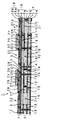
本発明を適用した高周波モジュール装置の一例を図1に示す。なお、図1は、この高周波モジュール装置1の構造を示す断面図である。
【0018】
この高周波モジュール装置1は、マザーボード(ベース基板)やインターポーザ(中間基板)に対する高密度実装を実現するためのパッケージ形態(BGA等)を有し、この装置自体が1つの機能部品として動作するものである。
【0019】
詳述すると、この高周波モジュール装置1は、ベース基板部2と、このベース基板部2の最上層が平坦化層3により平坦化され、この上に高周波素子部4とを備えている。
【0020】
ベース基板部2は、いわゆるプリント配線基板であり、誘電絶縁層となる第1の誘電基板5の両面に、パターン配線層となる第1及び第2の配線層6a,6bが形成された第1の配線基板7と、誘電絶縁層となる第2の誘電基板8の両面に、パターン配線層となる第3及び第4の配線層9a,9bが形成された第2の配線基板10とが、誘電絶縁層となるプリプレグ(接着樹脂)11を介して貼り合わされた構造を有している。
【0021】
このうち、第1の誘電基板5及び第2の誘電基板8は、低誘電率且つ低損失(低tanδ)な材料、すなわち高周波特性に優れた材料により形成されていることが好ましく、このような材料として、例えばポリフェニールエチレン(PPE)や、ビスマレイドトリアジン(BT−resin)、ポリテトラフルオロエチレン、ポリイミド、液晶ポリマー(LCP)、ポリノルボルネン(PNB)等の有機材料や、セラミック或いはセラミックと有機材料との混合材料等を挙げることができる。また、第1の誘電基板5及び第2の誘電基板8は、上述した材料の他に、耐熱性及び耐薬品性を有する材料により形成されていることが好ましく、このような材料からなる誘電基板として、廉価なエポキシ系基板FR−5等を挙げることができる。
【0022】
第1及び第2の配線層6a,6b並びに第3及び第4の配線層9a,9bは、例えばフィルタ12やキャパシタ13といった機能素子と、これらを繋ぐ信号配線パターン14や、電源パターン15及びグランドパターン16とが、例えば銅箔により薄膜形成されてなる。また、第1及び第2の配線層6a,6b並びに第3及び第4の配線層9a,9bとしては、インダクタやレジスタといった受動素子や、アンテナパターン等も形成可能である。
【0023】
また、各機能素子は、これらを繋ぐ信号配線パターン14や、電源パターン15及びグランドパターン16と、第1の誘電基板5及び第2の誘電基板8を貫通して形成された、例えば銅からなるビアホール17やスルーホール18を介して電気的に接続されている。具体的に、これらビアホール17やスルーホール18は、ベース基板部2の一部に、このベース基板部2を貫通する孔をドリル加工やレーザー加工により穿設し、この穿設された孔にビアメッキやスルーホールメッキを施すことにより形成される。
【0024】
このベース基板部2では、廉価な有機材料からなる第1の配線基板7及び第2の配線基板10を従来と同様の多層基板化技術によって積層形成することで、従来のような比較的高価とされるSi基板やガラス基板を用いた場合と比べて、コストの低減化が図られている。
【0025】
なお、このベース基板部2は、上述した構造のものに限定されず、その積層数についても任意である。また、ベース基板部2は、上述した両面配線基板7,10をプリプレグ11を介して貼り合わせたものに限定されず、例えば両面配線基板の両主面側に樹脂付銅箔を積み重ねていく構造のものであってもよい。
【0026】
平坦化層3は、ベース基板部2の最上層、すなわち第2の誘電基板8の第4の配線層9b側を高度に平坦化することにより、いわゆるビルドアップ形成面を形成している。具体的に、ビルドアップ形成面を形成する際は、ベース基板部2の最上層の全面に亘って、高周波特性に優れた有機材料からなる絶縁膜を成膜した後に、この最上層に形成された第4の配線層9bが露出するまで研磨する。これにより、第2の誘電基板8と第4の配線層9bとの間に絶縁膜が埋め込まれ、第2の誘電基板8上の第4の配線層9bが形成されていない部分との段差が無くなり、このベース基板部2の最上層が平坦化層3によって高度に平坦化されることになる。
【0027】
高周波素子部4は、このビルドアップ形成面上に絶縁層19が積層され、この積層された絶縁層19の内層或いは外層に、薄膜形成技術や厚膜形成技術によって、例えばインダクタ20,21,22,23や、キャパシタ、レジスタ等といった受動素子と、これらを繋ぐ配線パターン24及び埋め込み導体25とがパターン配線層として形成されてなる。
【0028】
このうち、絶縁層19は、低誘電率且つ低損失(低tanδ)な材料、すなわち高周波特性に優れた有機材料により形成されていることが好ましく、また、耐熱性及び耐薬品性を有する有機材料により形成されていることが好ましい。このような有機材料としては、例えばベンゾシクロブテン(BCB)や、ポリイミド、ポリノルボルネン(PNB)、液晶ポリマー(LCP)、エポキシ系樹脂、アクリル系樹脂等を挙げることができる。そして、絶縁層19は、このような有機材料を、例えばスピンコート法や、カーテンコート法、ロールコート法、ディップコート法等の塗布均一性及び膜厚制御に優れた方法を用いて、ビルドアップ形成面上に精度良く形成することができる。
【0029】
また、この高周波素子部4の最上層には、半導体チップ26がフリップチップ接続により搭載されている。ここで、フリップチップ接続は、半導体チップ26側の電極上にバンプ27を形成し、表裏逆にして高周波素子部4側の配線パターン24の電極28とバンプ27とを位置合わせし、加熱溶融することで、いわゆるフェースダウンボンディングで接続する実装方法である。このフリップチップ接続によれば、例えばワイヤーボンディングの比べてワイヤーの引き回し空間が不要となり、特に高さ方向の寸法を大幅に削減することができる。
【0030】
そして、これら高周波素子部4に形成された受動素子及び半導体チップ26は、配線パターン24及び埋め込み導体25を介して、ベース基板部2側の第4の配線層9bと電気的に接続されている。
【0031】
この高周波モジュール装置1では、ベース基板部2が多層化されることによって、高周波素子部4における積層数を削減することができる。すなわち、この高周波モジュール装置1では、高周波素子部4の内層或いは外層に形成された、例えば受動素子や配線パターン24、埋め込み導体25等のパターン配線層とは別に、ベース基板部2の内層或いは外層に、例えば機能素子や信号配線パターン14等のパターン配線層が形成されることによって、これらを従来のようなSi基板やガラス基板上にまとめて形成する場合に比べて、高周波素子部4にかかる負担を大幅に低減することができる。これにより、高周波素子部4の積層数を低減することが可能となり、装置全体のさらなる小型化及び低コスト化が可能となっている。
【0032】
また、この高周波モジュール装置1では、上述したベース基板部2のパターン配線層と高周波素子部4のパターン配線層とが分離されることによって、これらパターン配線層の間で発生する電気的干渉を抑制することができ、その特性の向上を図ることができる。
【0033】
さらに、この高周波モジュール装置1では、ベース基板部2の最上層が平坦化層3により高度に平坦化されたビルドアップ形成面が形成されていることから、このビルドアップ形成面上に高周波素子部4を精度良く形成することができる。
【0034】
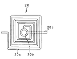
ところで、この高周波モジュール装置1には、ベース基板部2の第1及び第2の配線層6a,6b並びに第3及び第4の配線層9a,9bが形成されていない領域(以下、配線禁止領域という。)30,31,32,33が、少なくともベース基板部2の最上層から厚み方向の中途部に亘って或いはベース基板部2を貫通して設けられている。そして、この配線禁止領域30,31,32,33の直上に位置する高周波素子部4に、インダクタ20,21,22,23がそれぞれ形成されている。
【0035】
具体的に、配線禁止領域30は、図2に示すように、インダクタ20の形成位置から第2の配線層6bに至る領域に亘って設けられている。
【0036】
すなわち、第4の配線層9bには、図2及び図3(a)に示すように、インダクタ20が形成される領域に対応した第1の配線禁止用孔34が穿設されていると共に、第3の配線層9aには、図2及び図3(b)に示すように、インダクタ20が形成される領域に対応した第2の配線禁止用孔35が穿設されている。そして、図2及び図3(c)に示すように、これら第1の配線禁止用孔34及び第2の配線禁止用孔35を通して、第2の配線層6bに形成されたグランドパターン16とインダクタ20とが、所定の距離だけ離された状態で対向配置されている。
【0037】
一方、インダクタ20は、図2及び図4に示すように、絶縁層19の内層或いは外層に位置して、角形スパイラル状に巻回されてなる薄膜コイルパターン20aと、この薄膜コイルパターン20aの内周側の端部と電気的に接続された埋め込み導体パターン20bと、この埋め込み導体パターン20bと電気的に接続された引き出し導体パターン20cとを有し、この引き出し導体パターン20cが、薄膜コイルパターン20aの外周側へと引き出され、この薄膜コイルパターン20aの外周側の端部と共に、埋め込み導体25を介して配線パターン24とそれぞれ電気的に接続された構造とされている。
【0038】
具体的に、このインダクタ20を形成する際は、先ず、図2に示すように、平坦化されたベース基板部2上に、上述した有機材料からなる第1の絶縁層19aを形成する。
【0039】
次に、図2及び図5(a)に示すように、第1の絶縁層19a上に、例えばNiや銅等からなる導電膜を全面に亘って成膜した後に、フォトリソグラフィ技術を用いて所定の形状にパターニングされたフォトレジストをマスクとして、この導電膜をエッチングすることによって、引き出し導体パターン20cのベースを形成する。そして、例えば硫酸銅溶液を用いた電解メッキにより、数μm程度のCuからなる導電膜を成膜することで、引き出し導体パターン20cを形成する。
【0040】
次に、図2及び図5(b)に示すように、この引き出し導体パターン20cが形成された第1の絶縁層19a上に、上述した有機材料からなる第2の絶縁層19bを形成した後に、フォトリソグラフィ技術を用いて所定の形状にパターニングされたフォトレジストをマスクとしてエッチングを行い、引き出し導体パターン20cの端部と接合される部分が露出するビア(孔)を形成する。そして、このフォトレジストを残したまま、例えば硫酸銅溶液を用いた電解メッキにより、Cuからなる導電膜を成膜した後、フォトレジストを、このフォトレジスト上に堆積した導電膜と共に除去する。これにより、第2の絶縁層19bに埋め込まれた埋め込み導体パターン20bと、引き出し導体パターン20cとが電気的に接続される。
【0041】
次に、図2及び図5(c)に示すように、この第2の絶縁層19b上に、例えばNiや銅等からなる導電膜を全面に亘って成膜した後に、フォトリソグラフィ技術を用いて所定の形状にパターニングされたフォトレジストをマスクとして、この導電膜をエッチングすることによって、薄膜コイルパターン20aのベースを形成する。そして、例えば硫酸銅溶液を用いた電解メッキにより、数μm程度のCuからなる導電膜を成膜することで、埋め込み導体パターン20bと電気的に接続された薄膜コイルパターン20aを形成する。以上により、図2及び図4に示すようなインダクタ20が形成される。
【0042】
ここで、図2に示すように、インダクタ20の厚みAは、10μm以上且つ巻回間隔Bの1.5倍以下の範囲とすることが好ましい。
【0043】
このインダクタ20は、上述したメッキ法を用いることにより、従来のようなスパッタリング法を用いた場合(通常、0.5〜2μm程度の膜厚)に比べて、その厚みAを厚く形成することができる。そして、インダクタ20の厚みAを10μm以上とすることにより、このインダクタ20の直列抵抗が低減され、インダクタ20の高いQ値を得ることができる。一方、インダクタ20の厚みAを巻回間隔B、すなわち薄膜コイルパターン20aにおける隣接するパターン同士の間隔Bの1.5倍以下とすることにより、このインダクタ20を精度良く形成することができる。
【0044】
なお、このインダクタ20は、上述したメッキ法以外の厚膜技術を用いて、所定の厚みAで形成することも可能である。
【0045】
また、インダクタ20は、図4に示すような角形スパイラル状に巻回されたものに限定されず、例えば図6に示すような円形スパイラル状に巻回されたものであってもよい。
【0046】
なお、他のインダクタ21,22,23についても、上記インダクタ20と同様な形状を有しており、また、上記インダクタ20と同様にして形成されることから、以下説明を省略するものとする。
【0047】
以上のように、この高周波モジュール装置1では、ベース基板部2の配線禁止領域30,31,32,33が、少なくともベース基板部2の最上層から厚み方向の中途部に亘って或いはベース基板部2を貫通して設けられている。そして、この配線禁止領域30,31,32,33の直上に位置する高周波素子部4に、インダクタ20,21,22,23がそれぞれ形成されている。
【0048】
これにより、高周波モジュール装置1では、インダクタ20,22,23と、グランドパターン16との間の距離を離すことができ、これらインダクタ20,22,23と、グランドパターン16との結合容量を大幅に低減することができる。さらに、インダクタ21は、ベース基板部2を貫通して設けられた配線禁止領域31上に形成されていることから、さらなる特性の向上が図られている。
【0049】
したがって、これらインダクタ20,21,22,23の高いQ値を得ることができ、従来のようなインダクタの直下に位置してSi基板に穴を形成することや、このインダクタ素子を浮かせた状態で形成するといった加工を行わずとも、簡便な構成によってインダクタ20,21,22,23の良好な特性を得ることができる。以上のことから、この高周波モジュール装置1では、インダクタ20,21,22,23のさらなる特性向上が可能であると共に、さらなる小型化及び低コスト化が可能である。
【0050】
【発明の効果】
以上詳細に説明したように、本発明に係る高周波モジュール装置では、ベース基板部の高周波素子部に形成されたインダクタ素子と対向する領域が最上層から所定の厚みに亘る内層をパターン配線層が形成されていない配線禁止領域として構成することから、インダクタ素子とパターン配線層とが層間間隔を充分に保持されインダクタ素子の結合容量が低減されて高いQ値を得ることが可能となる。高周波モジュール装置は、廉価な有機材料からなる基板を用いてプリント配線技術によりパターン配線層と誘電絶縁層とを多層に形成したベース基板部の最上層を平坦化してビルドアップ形成面とし高周波素子部を積層形成することから、高精度のインダクタ素子を有してコスト低減が図られ、またマザーボード等に対して高密度実装されることで小型化が図られるようにする。
【図面の簡単な説明】
【図1】本発明を適用した高周波モジュール装置の一例を示す断面図である。
【図2】上記高周波モジュール装置における配線禁止領域及びインダクタの形成部分を拡大して示す要部断面図である。
【図3】ベース基板部の各層における配線禁止領域の構造を示す平面図であり、(a)は、第2の配線層における配線禁止領域を示し、(b)は、第3の配線層における配線禁止領域を示し、(c)は、第4の配線層における配線禁止領域を示す。
【図4】インダクタの構造を示す平面図である。
【図5】高周波素子部の各層におけるインダクタの構造を示す平面図であり、(a)は、第1の絶縁層上に形成された引き出し導体パターンを示し、(b)は、第2の絶縁層内に埋め込み形成された埋め込み導体パターンを示し、(c)は、第2の絶縁層上に形成された薄膜コイルパターンを示す。
【図6】インダクタの変形例を示す平面図である。
【符号の説明】
1 高周波モジュール装置、2 ベース基板部、3 平坦化層、4 高周波素子部、5 第1の誘電基板、6a,6b 第1の配線層、7 第1の配線基板、8 第2の誘電基板、9a,9b 第2の配線層、10 第2の配線基板、11プリプレグ、12 フィルタ、13 キャパシタ、14 信号配線パターン、15 電源パターン、16 グランドパターン、17 ビアホール、18 スルーホール、19 絶縁層、19a 第1の絶縁層、19b 第2の絶縁層、20インダクタ、20a 薄膜コイルパターン、20b 埋め込み導体パターン、20c 引き出し導体パターン、21,22,23 インダクタ、24 配線パターン、25 埋め込み導体、26 半導体チップ、30,31,32,33 配線禁止領域、34 第1の配線禁止用孔、35 第2の配線禁止用孔[0001]
BACKGROUND OF THE INVENTION
The present invention relates to a high-frequency module device that is mounted on various electronic devices such as a personal computer, a mobile phone, and an audio device, and has an information communication function, a storage function, and the like and constitutes a micro communication function module.
[0002]
[Prior art]
For example, various types of information such as music, voice, and images can be easily handled by personal computers, mobile computers, and the like in recent years as data is digitized. In addition, these information are band-compressed by audio codec technology and image codec technology, and an environment is being prepared in which digital communication and digital broadcasting are easily and efficiently distributed to various communication terminal devices. . For example, audio / video data (AV data) can be received outdoors by a mobile phone.
[0003]
By the way, a data transmission / reception system has been used in various ways by proposing a suitable network system even in a small area such as a home. As a network system, for example, a narrow band wireless communication system of 5 GHz band proposed by IEEE802.1a, a wireless LAN system of 2.45 GHz band proposed by IEEE802.1b, or Bluetooth is used. Various next-generation wireless systems such as distance wireless communication systems are attracting attention. The transmission / reception system makes effective use of such a wireless network system to easily exchange various data in various places such as home and outdoors, without using a relay device, access to the Internet network, and transmission / reception of data. Is possible.
[0004]
On the other hand, in the transmission / reception system, it is essential to realize a small, lightweight and portable communication terminal device having the above-described communication function. In a communication terminal device, since it is necessary to perform modulation / demodulation processing of an analog high-frequency signal in a transmission / reception unit, a high-frequency transmission / reception circuit using a superheterodyne method that is generally converted from a transmission / reception signal to an intermediate frequency is provided. .
[0005]
The high-frequency transmission / reception circuit includes an antenna unit that has an antenna and a changeover switch and receives or transmits an information signal, and a transmission / reception switcher that switches between transmission and reception. The high-frequency transmission / reception circuit includes a reception circuit unit including a frequency conversion circuit unit and a demodulation circuit unit. The high-frequency transmission / reception circuit includes a transmission circuit unit including a power amplifier, a drive amplifier, a modulation circuit unit, and the like. The high-frequency transmission / reception circuit includes a reference frequency generation circuit unit that supplies a reference frequency to the reception circuit unit and the transmission circuit unit.
[0006]
In such a high-frequency transmission / reception circuit, various filters, local oscillators (VCO), SAW (Surface acoustic wave) A large number of functional parts such as filters and passive parts such as inductors, resistors, capacitors and the like peculiar to high-frequency analog circuits such as matching circuits and bias circuits. In the high-frequency transmission / reception circuit, each circuit unit is made into an IC. However, a filter inserted between each stage cannot be incorporated in the IC, and for this reason, a matching circuit is also required as an external device. Therefore, the high-frequency transmission / reception circuit is large in size as a whole, which has been a major obstacle to reducing the size and weight of communication terminal equipment.
[0007]
On the other hand, a high frequency transmission / reception circuit based on a direct conversion system that transmits / receives an information signal without performing conversion to an intermediate frequency is also used for the communication terminal device. In such a high-frequency transmission / reception circuit, the information signal received by the antenna unit is supplied to the demodulation circuit unit via the transmission / reception switch, and direct baseband processing is performed. In a high-frequency transmission / reception circuit, an information signal generated by a source source is directly modulated to a predetermined frequency band without being converted to an intermediate frequency in a modulation circuit unit, and transmitted from an antenna unit via an amplifier and a transmission / reception switch. .
[0008]
Since such a high-frequency transmission / reception circuit is configured to transmit and receive information signals by performing direct detection without converting intermediate frequencies, the number of components such as filters is reduced, and the overall configuration is simplified. A configuration close to one chip is expected. However, also in the high frequency transmission / reception circuit by this direct conversion method, it is necessary to cope with a filter or a matching circuit arranged in the subsequent stage. In addition, since the high-frequency transmission / reception circuit performs amplification once at the high-frequency stage, it is difficult to obtain a sufficient gain, and it is necessary to perform an amplification operation also in the baseband portion. Therefore, the high-frequency transmission / reception circuit requires a DC offset cancel circuit and an extra low-pass filter, and has a problem that the overall power consumption increases.
[0009]
[Problems to be solved by the invention]
As described above, conventional high-frequency transmission / reception circuits cannot satisfy sufficient characteristics with respect to required specifications such as miniaturization and weight reduction of communication terminal equipment in both the superheterodyne method and the direct conversion method. . For this reason, various attempts have been made to make the high-frequency transmission / reception circuit into a module that is reduced in size with a simple configuration based on, for example, a Si-CMOS circuit. That is, as one of such attempts, for example, a passive element with good characteristics is formed on a Si substrate, a filter circuit, a resonator, and the like are formed on an LSI, and a logic LSI in the baseband portion is also integrated. A high-frequency module device made into one chip is proposed.
[0010]
However, in such a high-frequency module device, in order to improve the characteristics of the inductor element, a hole is formed in the Si substrate located immediately below the inductor element, or the inductor element is in a floating state. However, there is a problem that the processing cost increases.
[0011]
When the high-frequency signal circuit front end is formed on a semiconductor substrate such as Si or SiGe or a glass substrate, in addition to the high-frequency signal circuit pattern, a power supply pattern and a ground pattern, and a control signal wiring are used as a pattern wiring layer. It is necessary to form a pattern and the like, and these pattern wiring layers are multilayered, thereby causing problems such as mutual interference between pattern wiring layers and an increase in processing cost.
[0012]
In addition, when considering packaging of the entire module, such a high-frequency module device can be further mounted on an interposer (intermediate substrate) by wire bonding or the like, but the mounting area and the dimension in the thickness direction increase. Therefore, it was not always preferable from the viewpoint of cost.
[0013]
Therefore, the present invention has been proposed in view of such conventional circumstances, and provides a high-frequency module device that enables further improvement in characteristics of the inductor element and further reduction in size and cost. For the purpose.
[0014]
[Means for Solving the Problems]
The high-frequency module device according to the present invention that achieves this object,A base substrate portion formed by flattening the uppermost layer to form a build-up formation surface, and a high-frequency element portion laminated on the build-up formation surface with respect to the base substrate portion. The high-frequency module device is constructed by forming a base substrate portion on a substrate made of an organic material, in which signal wiring patterns, power supply patterns, or pattern wiring layers made of a ground pattern and dielectric insulating layers are alternately formed in multiple layers, and the uppermost layer is flattened. In addition to forming an up-formed surface, high-density mounting is performed on a mother board or an interposer via a wiring layer on the bottom surface side connected to the pattern wiring layer via a via hole or a through hole. In the high-frequency module device, the high-frequency element part is formed on the build-up forming surface of the base substrate part via an insulating layer, and the inductor element connected to the uppermost pattern wiring layer of the base substrate part via the embedded conductor Formed.
[0015]
High frequency module deviceIn this case, the region where the base substrate portion faces the inductor element formed in the high-frequency element portion is configured as a wiring prohibition region in which the inner layer extending from the uppermost layer to a predetermined thickness is not formed with the pattern wiring layer. In the high-frequency module device, a ground pattern is formed in the lower layer of the wiring prohibited area. In the high-frequency module device, the inductor element of the high-frequency element section can sufficiently maintain the interlayer spacing with the pattern wiring layer of the base substrate section, particularly the ground pattern, and can reduce the coupling capacitance and obtain a high Q value. Become.
[0016]
DETAILED DESCRIPTION OF THE INVENTION
Hereinafter, embodiments of the present invention will be described in detail with reference to the drawings.
[0017]
An example of a high-frequency module device to which the present invention is applied is shown in FIG. FIG. 1 is a cross-sectional view showing the structure of the high-
[0018]
The high-
[0019]
More specifically, the high-
[0020]
The
[0021]
Of these, the first
[0022]
The first and second wiring layers 6a and 6b and the third and fourth wiring layers 9a and 9b include functional elements such as a
[0023]
Each functional element is made of, for example, copper formed through the
[0024]
In this
[0025]
The
[0026]
The
[0027]
In the high-
[0028]
Of these, the insulating
[0029]
A
[0030]
The passive elements and the
[0031]
In the high-
[0032]
Further, in the high
[0033]
Further, in the high
[0034]
By the way, in the high-
[0035]
Specifically, as shown in FIG. 2, the
[0036]
That is, as shown in FIGS. 2 and 3A, the fourth wiring layer 9b is provided with a first
[0037]
On the other hand, as shown in FIGS. 2 and 4, the
[0038]
Specifically, when forming the
[0039]
Next, as shown in FIGS. 2 and 5A, a conductive film made of, for example, Ni or copper is formed over the entire surface of the first insulating layer 19a, and then photolithography is used. Using the photoresist patterned in a predetermined shape as a mask, this conductive film is etched to form the base of the
[0040]
Next, as shown in FIGS. 2 and 5B, after the second insulating
[0041]
Next, as shown in FIGS. 2 and 5C, a conductive film made of, for example, Ni or copper is formed over the entire surface of the second insulating
[0042]
Here, as shown in FIG. 2, the thickness A of the
[0043]
The
[0044]
The
[0045]
Further, the
[0046]
The
[0047]
As described above, in the high-
[0048]
Thereby, in the high
[0049]
Therefore, a high Q value of these
[0050]
【The invention's effect】
As described in detail above, in the high-frequency module device according to the present invention,Since the area facing the inductor element formed in the high-frequency element part of the base substrate part is configured as the wiring prohibition area in which the pattern wiring layer is not formed, the inner layer extending from the uppermost layer to a predetermined thickness is formed. Layer andButInterlayer spacingTheSufficiently held, the coupling capacitance of the inductor element is reduced, and a high Q value can be obtained. The high-frequency module device uses a substrate made of an inexpensive organic material to flatten the uppermost layer of the base substrate portion in which the pattern wiring layer and the dielectric insulating layer are formed in multiple layers by printed wiring technology, thereby forming a build-up formation surface, and the high-frequency element portion Therefore, it is possible to reduce the cost by having a highly accurate inductor element and to achieve miniaturization by high-density mounting on a motherboard or the like.
[Brief description of the drawings]
FIG. 1 is a cross-sectional view showing an example of a high-frequency module device to which the present invention is applied.
FIG. 2 is an essential part cross-sectional view showing, in an enlarged manner, a wiring prohibited region and an inductor formation part in the high-frequency module device.
FIGS. 3A and 3B are plan views showing a structure of a wiring prohibited area in each layer of the base substrate portion, wherein FIG. 3A shows a wiring prohibited area in the second wiring layer, and FIG. 3B shows a structure in the third wiring layer; A wiring prohibited area is shown, and (c) shows a wiring prohibited area in the fourth wiring layer.
FIG. 4 is a plan view showing the structure of an inductor.
5A is a plan view showing the structure of an inductor in each layer of a high-frequency element portion, FIG. 5A is a drawing conductor pattern formed on a first insulating layer, and FIG. 5B is a second insulating pattern; The embedded conductor pattern embedded in the layer is shown, and (c) shows the thin film coil pattern formed on the second insulating layer.
FIG. 6 is a plan view showing a modification of the inductor.
[Explanation of symbols]
DESCRIPTION OF
Claims (1)
上記ベース基板部のビルドアップ形成面上に絶縁層を介して形成され、埋め込み導体を介して上記ベース基板部の最上層のパターン配線層と接続されたインダクタ素子が形成されてなる高周波素子部とを備え、
上記ベース基板部が、上記高周波素子部に形成された上記インダクタ素子と対向する領域を、上記最上層から所定の厚みに亘る内層を上記パターン配線層が形成されていない配線禁止領域として構成するとともに、この配線禁止領域の下層位置に上記グランドパターンを形成していることを特徴とする高周波モジュール装置。Pattern wiring layers consisting of signal wiring patterns, power supply patterns or ground patterns and dielectric insulating layers are alternately formed in a multilayer on a substrate made of organic material , and the top layer is flattened to form a build-up formation surface, and via holes and A base substrate portion that is densely mounted on a motherboard or an interposer via a wiring layer on the bottom surface side connected to the pattern wiring layer via a through hole ;
A high-frequency element unit formed on the build-up forming surface of the base substrate unit through an insulating layer and formed with an inductor element connected to the uppermost pattern wiring layer of the base substrate unit via a buried conductor ; With
The base substrate portion constitutes a region facing the inductor element formed in the high-frequency element portion, and an inner layer extending from the uppermost layer to a predetermined thickness is configured as a wiring prohibited region in which the pattern wiring layer is not formed. The high-frequency module device is characterized in that the ground pattern is formed in a lower layer position of the wiring prohibited area .
Priority Applications (5)
| Application Number | Priority Date | Filing Date | Title |
|---|---|---|---|
| JP2001136490A JP3666411B2 (en) | 2001-05-07 | 2001-05-07 | High frequency module device |
| US10/332,015 US6800936B2 (en) | 2001-05-07 | 2002-05-02 | High-frequency module device |
| KR1020037000054A KR100862544B1 (en) | 2001-05-07 | 2002-05-02 | High-frequency module device |
| PCT/JP2002/004409 WO2002091405A1 (en) | 2001-05-07 | 2002-05-02 | High-frequency module device |
| EP02724688A EP1387369A4 (en) | 2001-05-07 | 2002-05-02 | High-frequency module device |
Applications Claiming Priority (1)
| Application Number | Priority Date | Filing Date | Title |
|---|---|---|---|
| JP2001136490A JP3666411B2 (en) | 2001-05-07 | 2001-05-07 | High frequency module device |
Publications (2)
| Publication Number | Publication Date |
|---|---|
| JP2002334806A JP2002334806A (en) | 2002-11-22 |
| JP3666411B2 true JP3666411B2 (en) | 2005-06-29 |
Family
ID=18983757
Family Applications (1)
| Application Number | Title | Priority Date | Filing Date |
|---|---|---|---|
| JP2001136490A Expired - Lifetime JP3666411B2 (en) | 2001-05-07 | 2001-05-07 | High frequency module device |
Country Status (5)
| Country | Link |
|---|---|
| US (1) | US6800936B2 (en) |
| EP (1) | EP1387369A4 (en) |
| JP (1) | JP3666411B2 (en) |
| KR (1) | KR100862544B1 (en) |
| WO (1) | WO2002091405A1 (en) |
Cited By (1)
| Publication number | Priority date | Publication date | Assignee | Title |
|---|---|---|---|---|
| US10193518B2 (en) | 2014-09-18 | 2019-01-29 | Murata Manufacturing Co., Ltd. | Radio-frequency (RF) component |
Families Citing this family (80)
| Publication number | Priority date | Publication date | Assignee | Title |
|---|---|---|---|---|
| US6143981A (en) | 1998-06-24 | 2000-11-07 | Amkor Technology, Inc. | Plastic integrated circuit package and method and leadframe for making the package |
| US20070176287A1 (en) * | 1999-11-05 | 2007-08-02 | Crowley Sean T | Thin integrated circuit device packages for improved radio frequency performance |
| KR100369393B1 (en) | 2001-03-27 | 2003-02-05 | 앰코 테크놀로지 코리아 주식회사 | Lead frame and semiconductor package using it and its manufacturing method |
| JP4604398B2 (en) * | 2001-06-11 | 2011-01-05 | ソニー株式会社 | High frequency module substrate device, high frequency module device and manufacturing method thereof |
| JP2003087007A (en) * | 2001-09-13 | 2003-03-20 | Sony Corp | High-frequency module substrate device |
| JP4318417B2 (en) * | 2001-10-05 | 2009-08-26 | ソニー株式会社 | High frequency module board device |
| US6873529B2 (en) * | 2002-02-26 | 2005-03-29 | Kyocera Corporation | High frequency module |
| US6936921B2 (en) * | 2002-11-11 | 2005-08-30 | Kyocera Corporation | High-frequency package |
| US7035113B2 (en) * | 2003-01-30 | 2006-04-25 | Endicott Interconnect Technologies, Inc. | Multi-chip electronic package having laminate carrier and method of making same |
| CA2455024A1 (en) | 2003-01-30 | 2004-07-30 | Endicott Interconnect Technologies, Inc. | Stacked chip electronic package having laminate carrier and method of making same |
| US6828514B2 (en) * | 2003-01-30 | 2004-12-07 | Endicott Interconnect Technologies, Inc. | High speed circuit board and method for fabrication |
| US7075167B2 (en) * | 2003-08-22 | 2006-07-11 | Agere Systems Inc. | Spiral inductor formed in a semiconductor substrate |
| JP4308073B2 (en) * | 2004-04-30 | 2009-08-05 | アルプス電気株式会社 | Signal receiving device |
| SG119329A1 (en) * | 2004-07-29 | 2006-02-28 | Fujikura Ltd | Semiconductor device and method for manufacturing the same |
| JP4717411B2 (en) * | 2004-10-18 | 2011-07-06 | 株式会社フジクラ | Semiconductor device |
| JP2006108644A (en) * | 2004-09-30 | 2006-04-20 | Endicott Interconnect Technologies Inc | High-speed circuit board for reducing stub of through hole, method of manufacturing the board, and information processing system using the board |
| JP4972306B2 (en) * | 2004-12-21 | 2012-07-11 | オンセミコンダクター・トレーディング・リミテッド | Semiconductor device and circuit device |
| US7750434B2 (en) * | 2005-01-31 | 2010-07-06 | Sanyo Electric Co., Ltd. | Circuit substrate structure and circuit apparatus |
| JP4185499B2 (en) * | 2005-02-18 | 2008-11-26 | 富士通マイクロエレクトロニクス株式会社 | Semiconductor device |
| WO2006106794A1 (en) | 2005-03-31 | 2006-10-12 | Semiconductor Energy Laboratory Co., Ltd. | Wireless chip and electronic device having wireless chip |
| US7742314B2 (en) * | 2005-09-01 | 2010-06-22 | Ngk Spark Plug Co., Ltd. | Wiring board and capacitor |
| JP2007142109A (en) | 2005-11-17 | 2007-06-07 | Tdk Corp | Electronic part |
| US7507603B1 (en) | 2005-12-02 | 2009-03-24 | Amkor Technology, Inc. | Etch singulated semiconductor package |
| US7968998B1 (en) | 2006-06-21 | 2011-06-28 | Amkor Technology, Inc. | Side leaded, bottom exposed pad and bottom exposed lead fusion quad flat semiconductor package |
| JP4722795B2 (en) * | 2006-08-31 | 2011-07-13 | 富士通株式会社 | Wiring board and electronic component module |
| DE102006057332B4 (en) * | 2006-12-05 | 2018-01-25 | Infineon Technologies Ag | Assembly comprising a substrate and a chip mounted on the substrate |
| US20080186123A1 (en) | 2007-02-07 | 2008-08-07 | Industrial Technology Research Institute | Inductor devices |
| US7982297B1 (en) | 2007-03-06 | 2011-07-19 | Amkor Technology, Inc. | Stackable semiconductor package having partially exposed semiconductor die and method of fabricating the same |
| JP4842200B2 (en) * | 2007-04-27 | 2011-12-21 | 株式会社日立製作所 | Printed circuit board with RFID tag |
| US7977774B2 (en) | 2007-07-10 | 2011-07-12 | Amkor Technology, Inc. | Fusion quad flat semiconductor package |
| US8018047B2 (en) * | 2007-08-06 | 2011-09-13 | Infineon Technologies Ag | Power semiconductor module including a multilayer substrate |
| US8154114B2 (en) * | 2007-08-06 | 2012-04-10 | Infineon Technologies Ag | Power semiconductor module |
| US7687899B1 (en) | 2007-08-07 | 2010-03-30 | Amkor Technology, Inc. | Dual laminate package structure with embedded elements |
| JP5114141B2 (en) * | 2007-09-13 | 2013-01-09 | イビデン株式会社 | Electronic component and manufacturing method thereof |
| TWI399139B (en) * | 2007-09-19 | 2013-06-11 | Ind Tech Res Inst | Meander inductor and printed circuit board with a meander inductor |
| US7777351B1 (en) | 2007-10-01 | 2010-08-17 | Amkor Technology, Inc. | Thin stacked interposer package |
| US8089159B1 (en) | 2007-10-03 | 2012-01-03 | Amkor Technology, Inc. | Semiconductor package with increased I/O density and method of making the same |
| US7847386B1 (en) | 2007-11-05 | 2010-12-07 | Amkor Technology, Inc. | Reduced size stacked semiconductor package and method of making the same |
| US7956453B1 (en) | 2008-01-16 | 2011-06-07 | Amkor Technology, Inc. | Semiconductor package with patterning layer and method of making same |
| US7723852B1 (en) | 2008-01-21 | 2010-05-25 | Amkor Technology, Inc. | Stacked semiconductor package and method of making same |
| US8067821B1 (en) | 2008-04-10 | 2011-11-29 | Amkor Technology, Inc. | Flat semiconductor package with half package molding |
| US7768135B1 (en) | 2008-04-17 | 2010-08-03 | Amkor Technology, Inc. | Semiconductor package with fast power-up cycle and method of making same |
| US7808084B1 (en) | 2008-05-06 | 2010-10-05 | Amkor Technology, Inc. | Semiconductor package with half-etched locking features |
| US8125064B1 (en) | 2008-07-28 | 2012-02-28 | Amkor Technology, Inc. | Increased I/O semiconductor package and method of making same |
| US8184453B1 (en) | 2008-07-31 | 2012-05-22 | Amkor Technology, Inc. | Increased capacity semiconductor package |
| US7847392B1 (en) | 2008-09-30 | 2010-12-07 | Amkor Technology, Inc. | Semiconductor device including leadframe with increased I/O |
| US7989933B1 (en) | 2008-10-06 | 2011-08-02 | Amkor Technology, Inc. | Increased I/O leadframe and semiconductor device including same |
| TW201021173A (en) * | 2008-10-08 | 2010-06-01 | Panasonic Corp | Interposer substrate and semiconductor device |
| US8008758B1 (en) | 2008-10-27 | 2011-08-30 | Amkor Technology, Inc. | Semiconductor device with increased I/O leadframe |
| US8089145B1 (en) | 2008-11-17 | 2012-01-03 | Amkor Technology, Inc. | Semiconductor device including increased capacity leadframe |
| US8072050B1 (en) | 2008-11-18 | 2011-12-06 | Amkor Technology, Inc. | Semiconductor device with increased I/O leadframe including passive device |
| US7875963B1 (en) | 2008-11-21 | 2011-01-25 | Amkor Technology, Inc. | Semiconductor device including leadframe having power bars and increased I/O |
| US7982298B1 (en) | 2008-12-03 | 2011-07-19 | Amkor Technology, Inc. | Package in package semiconductor device |
| US8487420B1 (en) | 2008-12-08 | 2013-07-16 | Amkor Technology, Inc. | Package in package semiconductor device with film over wire |
| US8680656B1 (en) | 2009-01-05 | 2014-03-25 | Amkor Technology, Inc. | Leadframe structure for concentrated photovoltaic receiver package |
| US20170117214A1 (en) | 2009-01-05 | 2017-04-27 | Amkor Technology, Inc. | Semiconductor device with through-mold via |
| US8058715B1 (en) | 2009-01-09 | 2011-11-15 | Amkor Technology, Inc. | Package in package device for RF transceiver module |
| US9000558B2 (en) * | 2009-01-19 | 2015-04-07 | Broadcom Corporation | Wafer-level flip chip package with RF passive element/ package signal connection overlay |
| US8026589B1 (en) | 2009-02-23 | 2011-09-27 | Amkor Technology, Inc. | Reduced profile stackable semiconductor package |
| US7960818B1 (en) | 2009-03-04 | 2011-06-14 | Amkor Technology, Inc. | Conformal shield on punch QFN semiconductor package |
| JP4893773B2 (en) * | 2009-04-02 | 2012-03-07 | 株式会社村田製作所 | Electronic component and manufacturing method thereof |
| US8575742B1 (en) | 2009-04-06 | 2013-11-05 | Amkor Technology, Inc. | Semiconductor device with increased I/O leadframe including power bars |
| US8427833B2 (en) * | 2010-10-28 | 2013-04-23 | International Business Machines Corporation | Thermal power plane for integrated circuits |
| US8405998B2 (en) | 2010-10-28 | 2013-03-26 | International Business Machines Corporation | Heat sink integrated power delivery and distribution for integrated circuits |
| US8253234B2 (en) | 2010-10-28 | 2012-08-28 | International Business Machines Corporation | Optimized semiconductor packaging in a three-dimensional stack |
| US8674485B1 (en) | 2010-12-08 | 2014-03-18 | Amkor Technology, Inc. | Semiconductor device including leadframe with downsets |
| US8648450B1 (en) | 2011-01-27 | 2014-02-11 | Amkor Technology, Inc. | Semiconductor device including leadframe with a combination of leads and lands |
| TWI557183B (en) | 2015-12-16 | 2016-11-11 | 財團法人工業技術研究院 | Siloxane resin composition, and photoelectric device employing the same |
| DE102011089639A1 (en) * | 2011-12-22 | 2013-06-27 | Siemens Aktiengesellschaft | Circuit carrier with a separate RF circuit and method for assembling such a circuit carrier |
| US9704725B1 (en) | 2012-03-06 | 2017-07-11 | Amkor Technology, Inc. | Semiconductor device with leadframe configured to facilitate reduced burr formation |
| US8907227B2 (en) * | 2012-08-02 | 2014-12-09 | Hong Kong Science and Technology Research Institute Company Limited | Multiple surface integrated devices on low resistivity substrates |
| KR101486790B1 (en) | 2013-05-02 | 2015-01-28 | 앰코 테크놀로지 코리아 주식회사 | Micro Lead Frame for semiconductor package |
| KR101563911B1 (en) | 2013-10-24 | 2015-10-28 | 앰코 테크놀로지 코리아 주식회사 | Semiconductor package |
| US9673122B2 (en) | 2014-05-02 | 2017-06-06 | Amkor Technology, Inc. | Micro lead frame structure having reinforcing portions and method |
| US9247647B1 (en) | 2014-09-11 | 2016-01-26 | Qualcomm Incorporated | High quality factor inductor and high quality factor filter in package substrate or printed circuit board (PCB) |
| JP6645109B2 (en) * | 2015-10-09 | 2020-02-12 | セイコーエプソン株式会社 | Liquid ejection device and drive circuit |
| US20170236790A1 (en) * | 2016-02-12 | 2017-08-17 | Semtech Corporation | Semiconductor Device on Leadframe with Integrated Passive Component |
| JP6669132B2 (en) * | 2017-06-23 | 2020-03-18 | 株式会社村田製作所 | Multiplexer, transmitting device and receiving device |
| US10700024B2 (en) * | 2017-08-18 | 2020-06-30 | Samsung Electro-Mechanics Co., Ltd. | Fan-out semiconductor package |
| TWI698008B (en) * | 2018-08-31 | 2020-07-01 | 英屬開曼群島商鳳凰先驅股份有限公司 | Integrated driving module with energy conversion function and manufacturing method thereof |
Family Cites Families (12)
| Publication number | Priority date | Publication date | Assignee | Title |
|---|---|---|---|---|
| DE3823469A1 (en) * | 1988-07-11 | 1990-01-18 | Bodenseewerk Geraetetech | FILTER ARRANGEMENT |
| US5215866A (en) * | 1989-08-09 | 1993-06-01 | Avantek, Inc. | Broadband printed spiral |
| US5483100A (en) * | 1992-06-02 | 1996-01-09 | Amkor Electronics, Inc. | Integrated circuit package with via interconnections formed in a substrate |
| TW424321B (en) * | 1996-10-31 | 2001-03-01 | Sharp Kk | Integrated electronic circuit |
| US6005197A (en) * | 1997-08-25 | 1999-12-21 | Lucent Technologies Inc. | Embedded thin film passive components |
| JP3381902B2 (en) | 1998-04-27 | 2003-03-04 | 株式会社村田製作所 | Manufacturing method of coil parts |
| JP3646540B2 (en) | 1998-10-02 | 2005-05-11 | 富士ゼロックス株式会社 | Low pass filter |
| US6303423B1 (en) * | 1998-12-21 | 2001-10-16 | Megic Corporation | Method for forming high performance system-on-chip using post passivation process |
| JP2000189937A (en) * | 1998-12-28 | 2000-07-11 | Matsushita Electric Ind Co Ltd | Environmental assessment system |
| US6274937B1 (en) * | 1999-02-01 | 2001-08-14 | Micron Technology, Inc. | Silicon multi-chip module packaging with integrated passive components and method of making |
| US6218729B1 (en) * | 1999-03-11 | 2001-04-17 | Atmel Corporation | Apparatus and method for an integrated circuit having high Q reactive components |
| JP4005762B2 (en) * | 1999-06-30 | 2007-11-14 | 株式会社東芝 | Integrated circuit device and manufacturing method thereof |
-
2001
- 2001-05-07 JP JP2001136490A patent/JP3666411B2/en not_active Expired - Lifetime
-
2002
- 2002-05-02 US US10/332,015 patent/US6800936B2/en not_active Expired - Lifetime
- 2002-05-02 KR KR1020037000054A patent/KR100862544B1/en active IP Right Grant
- 2002-05-02 EP EP02724688A patent/EP1387369A4/en not_active Withdrawn
- 2002-05-02 WO PCT/JP2002/004409 patent/WO2002091405A1/en active Application Filing
Cited By (1)
| Publication number | Priority date | Publication date | Assignee | Title |
|---|---|---|---|---|
| US10193518B2 (en) | 2014-09-18 | 2019-01-29 | Murata Manufacturing Co., Ltd. | Radio-frequency (RF) component |
Also Published As
| Publication number | Publication date |
|---|---|
| KR20030041951A (en) | 2003-05-27 |
| US20030148739A1 (en) | 2003-08-07 |
| US6800936B2 (en) | 2004-10-05 |
| EP1387369A1 (en) | 2004-02-04 |
| JP2002334806A (en) | 2002-11-22 |
| KR100862544B1 (en) | 2008-10-09 |
| WO2002091405A1 (en) | 2002-11-14 |
| EP1387369A4 (en) | 2009-08-19 |
Similar Documents
| Publication | Publication Date | Title |
|---|---|---|
| JP3666411B2 (en) | High frequency module device | |
| JP4318417B2 (en) | High frequency module board device | |
| US6714422B2 (en) | High frequency module device and method for its preparation | |
| US7741162B2 (en) | Method for manufacturing high-frequency module device | |
| US7599190B2 (en) | High-frequency module, and method of producing same | |
| WO2003047325A1 (en) | High-frequency circuit block, its manufacturing method, high-frequency module device, and its manufacturing method | |
| JP3941416B2 (en) | High frequency module device and manufacturing method thereof | |
| JP2003264348A (en) | High frequency module | |
| JP4608794B2 (en) | High frequency module device and manufacturing method thereof | |
| JP4211378B2 (en) | Capacitor element | |
| JP4595240B2 (en) | High frequency module substrate device and manufacturing method thereof |
Legal Events
| Date | Code | Title | Description |
|---|---|---|---|
| A131 | Notification of reasons for refusal |
Free format text: JAPANESE INTERMEDIATE CODE: A131 Effective date: 20040615 |
|
| A521 | Written amendment |
Free format text: JAPANESE INTERMEDIATE CODE: A523 Effective date: 20040810 |
|
| TRDD | Decision of grant or rejection written | ||
| A01 | Written decision to grant a patent or to grant a registration (utility model) |
Free format text: JAPANESE INTERMEDIATE CODE: A01 Effective date: 20050315 |
|
| A61 | First payment of annual fees (during grant procedure) |
Free format text: JAPANESE INTERMEDIATE CODE: A61 Effective date: 20050328 |
|
| R151 | Written notification of patent or utility model registration |
Ref document number: 3666411 Country of ref document: JP Free format text: JAPANESE INTERMEDIATE CODE: R151 |
|
| FPAY | Renewal fee payment (event date is renewal date of database) |
Free format text: PAYMENT UNTIL: 20080415 Year of fee payment: 3 |
|
| FPAY | Renewal fee payment (event date is renewal date of database) |
Free format text: PAYMENT UNTIL: 20090415 Year of fee payment: 4 |
|
| FPAY | Renewal fee payment (event date is renewal date of database) |
Free format text: PAYMENT UNTIL: 20090415 Year of fee payment: 4 |
|
| FPAY | Renewal fee payment (event date is renewal date of database) |
Free format text: PAYMENT UNTIL: 20100415 Year of fee payment: 5 |
|
| FPAY | Renewal fee payment (event date is renewal date of database) |
Free format text: PAYMENT UNTIL: 20100415 Year of fee payment: 5 |
|
| FPAY | Renewal fee payment (event date is renewal date of database) |
Free format text: PAYMENT UNTIL: 20110415 Year of fee payment: 6 |
|
| R250 | Receipt of annual fees |
Free format text: JAPANESE INTERMEDIATE CODE: R250 |
|
| FPAY | Renewal fee payment (event date is renewal date of database) |
Free format text: PAYMENT UNTIL: 20120415 Year of fee payment: 7 |
|
| R250 | Receipt of annual fees |
Free format text: JAPANESE INTERMEDIATE CODE: R250 |
|
| FPAY | Renewal fee payment (event date is renewal date of database) |
Free format text: PAYMENT UNTIL: 20130415 Year of fee payment: 8 |
|
| R250 | Receipt of annual fees |
Free format text: JAPANESE INTERMEDIATE CODE: R250 |
|
| FPAY | Renewal fee payment (event date is renewal date of database) |
Free format text: PAYMENT UNTIL: 20130415 Year of fee payment: 8 |
|
| FPAY | Renewal fee payment (event date is renewal date of database) |
Free format text: PAYMENT UNTIL: 20140415 Year of fee payment: 9 |
|
| R250 | Receipt of annual fees |
Free format text: JAPANESE INTERMEDIATE CODE: R250 |
|
| R250 | Receipt of annual fees |
Free format text: JAPANESE INTERMEDIATE CODE: R250 |
|
| R250 | Receipt of annual fees |
Free format text: JAPANESE INTERMEDIATE CODE: R250 |
|
| R250 | Receipt of annual fees |
Free format text: JAPANESE INTERMEDIATE CODE: R250 |
|
| R250 | Receipt of annual fees |
Free format text: JAPANESE INTERMEDIATE CODE: R250 |
|
| R250 | Receipt of annual fees |
Free format text: JAPANESE INTERMEDIATE CODE: R250 |
|
| R250 | Receipt of annual fees |
Free format text: JAPANESE INTERMEDIATE CODE: R250 |
|
| R250 | Receipt of annual fees |
Free format text: JAPANESE INTERMEDIATE CODE: R250 |