JP3639302B2 - Resin-sealed semiconductor device - Google Patents
Resin-sealed semiconductor device Download PDFInfo
- Publication number
- JP3639302B2 JP3639302B2 JP2004240416A JP2004240416A JP3639302B2 JP 3639302 B2 JP3639302 B2 JP 3639302B2 JP 2004240416 A JP2004240416 A JP 2004240416A JP 2004240416 A JP2004240416 A JP 2004240416A JP 3639302 B2 JP3639302 B2 JP 3639302B2
- Authority
- JP
- Japan
- Prior art keywords
- semiconductor device
- lead
- resin
- die pad
- sealing resin
- Prior art date
- Legal status (The legal status is an assumption and is not a legal conclusion. Google has not performed a legal analysis and makes no representation as to the accuracy of the status listed.)
- Expired - Lifetime
Links
Images


Classifications
-
- H—ELECTRICITY
- H01—ELECTRIC ELEMENTS
- H01L—SEMICONDUCTOR DEVICES NOT COVERED BY CLASS H10
- H01L2224/00—Indexing scheme for arrangements for connecting or disconnecting semiconductor or solid-state bodies and methods related thereto as covered by H01L24/00
- H01L2224/01—Means for bonding being attached to, or being formed on, the surface to be connected, e.g. chip-to-package, die-attach, "first-level" interconnects; Manufacturing methods related thereto
- H01L2224/42—Wire connectors; Manufacturing methods related thereto
- H01L2224/47—Structure, shape, material or disposition of the wire connectors after the connecting process
- H01L2224/48—Structure, shape, material or disposition of the wire connectors after the connecting process of an individual wire connector
- H01L2224/4805—Shape
- H01L2224/4809—Loop shape
- H01L2224/48091—Arched
-
- H—ELECTRICITY
- H01—ELECTRIC ELEMENTS
- H01L—SEMICONDUCTOR DEVICES NOT COVERED BY CLASS H10
- H01L2224/00—Indexing scheme for arrangements for connecting or disconnecting semiconductor or solid-state bodies and methods related thereto as covered by H01L24/00
- H01L2224/01—Means for bonding being attached to, or being formed on, the surface to be connected, e.g. chip-to-package, die-attach, "first-level" interconnects; Manufacturing methods related thereto
- H01L2224/42—Wire connectors; Manufacturing methods related thereto
- H01L2224/47—Structure, shape, material or disposition of the wire connectors after the connecting process
- H01L2224/48—Structure, shape, material or disposition of the wire connectors after the connecting process of an individual wire connector
- H01L2224/481—Disposition
- H01L2224/48151—Connecting between a semiconductor or solid-state body and an item not being a semiconductor or solid-state body, e.g. chip-to-substrate, chip-to-passive
- H01L2224/48221—Connecting between a semiconductor or solid-state body and an item not being a semiconductor or solid-state body, e.g. chip-to-substrate, chip-to-passive the body and the item being stacked
- H01L2224/48245—Connecting between a semiconductor or solid-state body and an item not being a semiconductor or solid-state body, e.g. chip-to-substrate, chip-to-passive the body and the item being stacked the item being metallic
- H01L2224/48247—Connecting between a semiconductor or solid-state body and an item not being a semiconductor or solid-state body, e.g. chip-to-substrate, chip-to-passive the body and the item being stacked the item being metallic connecting the wire to a bond pad of the item
Description
本発明は、半導体チップとこれに接続されるリードフレームとを樹脂で封止してなる樹脂封止型半導体装置に係り、特に信頼性の向上対策に関する。 The present invention relates to a resin-encapsulated semiconductor device in which a semiconductor chip and a lead frame connected to the semiconductor chip are encapsulated with resin, and more particularly to a measure for improving reliability.
近年、機器の小型・軽量化を目的として、プリント基板に実装する半導体製品の小型化・薄型化が強く要求されている。この目的を実現するために、例えば、ポリイミドテープを用いたTAB実装技術等が開発されている。しかし、現在でも、一般的な機器には、半導体チップとこれに接続されるリードフレームとを樹脂で封止してなる樹脂封止型半導体装置が汎用されている。 In recent years, there has been a strong demand for downsizing and thinning of semiconductor products mounted on a printed circuit board for the purpose of reducing the size and weight of devices. In order to realize this object, for example, a TAB mounting technique using a polyimide tape has been developed. However, at present, a resin-sealed semiconductor device in which a semiconductor chip and a lead frame connected to the semiconductor chip are sealed with a resin is widely used as a general device.
以下、現在汎用されている樹脂封止型半導体装置について説明する。図8は、従来の両面封止型の樹脂封止型半導体装置の一例を示す断面図である。 Hereinafter, resin-encapsulated semiconductor devices that are currently widely used will be described. FIG. 8 is a cross-sectional view showing an example of a conventional double-sided sealing type resin-sealed semiconductor device.
図8に示す従来の樹脂封止型半導体装置は、リードフレームのダイパッド102の上に半導体チップ103を搭載し、その半導体チップ103の電極パッド(図示せず)とリードフレームのインナーリード104とを金属細線105により電気的に接続している。そして、半導体チップ103、ダイパッド102、インナーリード104及び金属細線105が封止樹脂106内に封止されている。そして、インナーリード104につながり封止樹脂106の外方に突出しているアウターリード101がプリント配線板等に接続される外部電極端子となる。この構造では、半導体チップ103の上方とダイパッド102の下方との双方に封止樹脂106が存在することになるので、半導体装置全体の厚みが大きくなる欠点がある。
The conventional resin-encapsulated semiconductor device shown in FIG. 8 has a
そこで、図9及び図10に示す片面封止型半導体装置が考えられている。ただし、図9はインナーリード104が存在する断面における従来の片面封止型半導体装置の断面図であり、図10は従来の片面封止型半導体装置の裏面図である。図9及び図10に示す各部に用いられる材料・機能は図8におけると同じなので同一番号を付して、その説明は省略する。図9及び図10に示す片面封止型の半導体装置の構造では、封止樹脂106がダイパッド102の半導体チップ103を搭載している面側にのみ存在しているので、半導体装置全体の厚さを小さくすることができる。
しかしながら、上記図9及び図10に示す従来の樹脂封止型半導体装置においては、以下のような問題がある。 However, the conventional resin-encapsulated semiconductor device shown in FIGS. 9 and 10 has the following problems.
すなわち、片面封止型の半導体装置の場合、両面封止型の半導体装置に比べてインナーリード104の下方に封止樹脂が存在しないことから、インナーリード104に対する封止樹脂106の保持力がどうしても弱くなるので、図8に示す断面内においてインナーリード104に引っ張り力などの力が作用すると、インナーリード104が容易に封止樹脂から剥がれるおそれがある。特に、半導体チップ内に多数の半導体素子(トランジスタなど)を搭載して高密度化を図ることで、外部電極端子数が増大すると、プリント配線板にかかる曲げ応力により、半田等によって基板に取り付けられた半導体装置の外部電極端子がプリント配線板や封止樹脂から剥がれたり、実装後における半導体装置の温度サイクル耐性が低下したりするなど、信頼性の低下を招くおそれがある。
That is, in the case of a single-sided sealing type semiconductor device, the sealing
本発明は、半導体装置に印加される熱応力等の応力が、特に半導体装置のコーナー部に近づくほど顕著になる点に着目してなされたものである。 The present invention has been made paying attention to the point that stress such as thermal stress applied to a semiconductor device becomes more prominent as it approaches a corner portion of the semiconductor device.
本発明の第1の目的は、半導体装置の1つの辺における外部電極の配置密度を辺の中央部と端部(つまりコーナー部に近い部分)とで異ならせることにより、外部電極数の増大を図りつつ、封止樹脂と外部電極との間の接合力の強化を図ることにある。 The first object of the present invention is to increase the number of external electrodes by making the arrangement density of the external electrodes on one side of the semiconductor device different between the central portion and the end portion (that is, the portion close to the corner portion) of the side. The aim is to strengthen the bonding force between the sealing resin and the external electrode.
また、本発明の第2の目的は、半導体装置の1つの辺における外部電極の面積を辺の中央部と端部とで異ならせることにより、外部電極数の増大を図りつつ、外部電極とプリント配線板等の実装基板との間の接合力の強化を図ることにある。 The second object of the present invention is to increase the number of external electrodes while increasing the number of external electrodes by making the area of the external electrodes on one side of the semiconductor device different between the central part and the end part of the side. The purpose is to reinforce the bonding force with a mounting substrate such as a wiring board.
さらに、本発明の第3の目的は、半導体装置の各辺における外部電極の形状を利用することで、半導体装置の基準位置を識別を可能とし、実装基板への取り付けの容易化を図ることにある。 Furthermore, a third object of the present invention is to make it possible to identify the reference position of the semiconductor device by using the shape of the external electrode on each side of the semiconductor device, and to facilitate the attachment to the mounting substrate. is there.
上記の目的を達成するために、本発明の樹脂封止型半導体装置は、ダイパッドと、溝を有するリードと、ダイパッドに搭載された半導体チップと、半導体チップとリードとを電気的に接続する金属細線と、溝と、金属細線と、半導体チップと、リードの上面とを封止し、かつ、リードの下面の一部を露出する封止樹脂とを備え、溝は、リードの下面の露出部の上方に位置し、リードは、上方の幅が下方の幅よりも広い部分を有し、金属細線は、リードの溝の上でない部分であって、封止樹脂に封止された部分に接続される。In order to achieve the above object, a resin-encapsulated semiconductor device of the present invention includes a die pad, a lead having a groove, a semiconductor chip mounted on the die pad, and a metal that electrically connects the semiconductor chip and the lead. A thin wire, a groove, a metal thin wire, a semiconductor chip, and a sealing resin that seals the upper surface of the lead and exposes a part of the lower surface of the lead, and the groove is an exposed portion of the lower surface of the lead The lead has a portion where the upper width is wider than the lower width, and the fine metal wire is not on the lead groove and is connected to the portion sealed with the sealing resin Is done.
本発明の樹脂封止型半導体装置において、リードの下面の一部以外の部分が封止樹脂により封止されたことが好ましい。In the resin-encapsulated semiconductor device of the present invention, it is preferable that a portion other than a part of the lower surface of the lead is encapsulated with an encapsulating resin.
本発明の樹脂封止型半導体装置において、リードは、上面が下面よりも大きいことが好ましい。In the resin-encapsulated semiconductor device of the present invention, it is preferable that the upper surface of the lead is larger than the lower surface.
本発明の樹脂封止型半導体装置において、溝は、リードの上面に形成されていることが好ましい。In the resin-encapsulated semiconductor device of the present invention, the groove is preferably formed on the upper surface of the lead.
本発明の樹脂封止型半導体装置において、リードは、溝よりもダイパッド側に薄肉部を有し、薄肉部の厚みは、リードの下面の露出部とリードの溝を除く上面とで構成される厚みよりも薄いことが好ましい。In the resin-encapsulated semiconductor device of the present invention, the lead has a thin portion on the die pad side of the groove, and the thickness of the thin portion is constituted by the exposed portion on the lower surface of the lead and the upper surface excluding the groove of the lead. It is preferable that the thickness is smaller than the thickness.
本発明の樹脂封止型半導体装置において、薄肉部の下方に樹脂封止を有していることが好ましい。In the resin-encapsulated semiconductor device of the present invention, it is preferable that the resin-encapsulated semiconductor device has a resin seal below the thin portion.
本発明の樹脂封止型半導体装置において、半導体チップは、前記ダイパッドからはみ出して搭載されていることが好ましい。In the resin-encapsulated semiconductor device of the present invention, the semiconductor chip is preferably mounted so as to protrude from the die pad.
本発明の樹脂封止型半導体装置において、封止樹脂は、ダイパッドの下面を露出していることが好ましい。In the resin-encapsulated semiconductor device of the present invention, it is preferable that the encapsulating resin exposes the lower surface of the die pad.
本発明の樹脂封止型半導体装置において、封止樹脂の側面とリードの先端とがほぼ同一面であることが好ましい。In the resin-encapsulated semiconductor device of the present invention, it is preferable that the side surface of the encapsulating resin and the tip of the lead are substantially the same surface.
本発明の第1の半導体装置によれば、半導体チップ,リード及び接続部材をリードの下面を露出させた状態で封止樹脂内に封止した樹脂封止型半導体装置において、リードの下部を外部電極として機能させるとともに、半導体装置の裏面における外部電極の配列ピッチがコーナー部におけるよりも辺の中央部において小さい構造としたので、特に熱応力等の応力が強く作用するコーナー部におけるリードの抜け,剥がれ等の不具合を防止することにより、半導体装置内の半導体素子の高密度化を図りつつ、信頼性の向上を図ることができる。 According to the first semiconductor device of the present invention, in the resin-encapsulated semiconductor device in which the semiconductor chip, the lead, and the connection member are sealed in the sealing resin with the lower surface of the lead exposed, the lower portion of the lead is externally provided. In addition to functioning as an electrode, the arrangement pitch of the external electrodes on the back surface of the semiconductor device is smaller in the center part of the side than in the corner part. By preventing defects such as peeling, it is possible to improve the reliability while increasing the density of the semiconductor elements in the semiconductor device.
本発明の第2の半導体装置によれば、半導体チップ,リード及び接続部材をリードの下面を露出させた状態で封止樹脂内に封止した樹脂封止型半導体装置において、リードの下部を外部電極として機能させるとともに、半導体装置の裏面における外部電極の下面の面積が辺の中央部におけるよりもコーナー部において大きい構造としたので、特に熱応力等の応力が強く作用するコーナー部における実装基板との接合力を高めることにより、実装後における半導体装置の信頼性の向上を図ることができる。 According to the second semiconductor device of the present invention, in the resin-encapsulated semiconductor device in which the semiconductor chip, the lead, and the connection member are sealed in the sealing resin with the lower surface of the lead exposed, the lower portion of the lead is externally provided. In addition to functioning as an electrode, since the area of the lower surface of the external electrode on the back surface of the semiconductor device is larger in the corner portion than in the central portion of the side, the mounting substrate particularly in the corner portion where stress such as thermal stress acts strongly By increasing the bonding strength, it is possible to improve the reliability of the semiconductor device after mounting.
本発明の第3の半導体装置によれば、半導体チップ,リード及び接続部材をリードの下面を露出させた状態で封止樹脂内に封止した樹脂封止型半導体装置において、リードの下部を外部電極として機能させるとともに、各辺のうち1つの辺における少なくとも1つの外部電極の形状を半導体装置の基準位置の識別マークとなるように形成しておく構造としたので、半導体装置の検査時や実装基板への実装時における基準位置を容易かつ迅速に識別することができ、半導体装置の製造の容易化を図ることができる。 According to the third semiconductor device of the present invention, in the resin-encapsulated semiconductor device in which the semiconductor chip, the lead, and the connection member are sealed in the sealing resin with the lower surface of the lead exposed, the lower portion of the lead is externally provided. In addition to functioning as an electrode, the shape of at least one external electrode on one side of each side is formed so as to be an identification mark of a reference position of the semiconductor device. The reference position at the time of mounting on the substrate can be easily and quickly identified, and the manufacture of the semiconductor device can be facilitated.
本発明の第1のリードフレームによれば、上記第1の半導体装置の効果を実現するためのリードフレームの提供を図ることができる。 According to the first lead frame of the present invention, it is possible to provide a lead frame for realizing the effect of the first semiconductor device.
本発明の第2のリードフレームによれば、上記第2の半導体装置の作用効果を得るためのリードフレームの提供を図ることができる。 According to the second lead frame of the present invention, it is possible to provide a lead frame for obtaining the function and effect of the second semiconductor device.
以下、本発明の樹脂封止型半導体装置の実施形態について図面を参照しながら説明する。 Hereinafter, embodiments of the resin-encapsulated semiconductor device of the present invention will be described with reference to the drawings.
(第1の実施形態)
図1,図2及び図3は、それぞれ本発明の第1の実施形態に係る樹脂封止型半導体装置の構造を説明する断面図,上面図及び裏面図である。ただし、図2の平面図では、内部構造を理解しやすくするため、封止樹脂を透視した状態を示している。また、図1は、図2に示すI-I線における断面図である。
(First embodiment)
1, 2 and 3 are a sectional view, a top view and a back view for explaining the structure of the resin-encapsulated semiconductor device according to the first embodiment of the present invention, respectively. However, in the plan view of FIG. 2, the sealing resin is seen through in order to facilitate understanding of the internal structure. 1 is a cross-sectional view taken along the line II shown in FIG.
図1〜図3に示すように、本実施形態の樹脂封止型半導体装置は、リードフレームの一部である吊りリード10と、吊りリード10により支持されるダイパッド11と、ダイパッド11上に搭載され内部に多数の半導体素子を有する半導体チップ12と、先端が半導体チップ12の近傍に配置されたリード13と、半導体チップ12の主面上の電極パッド(図示せず)とリード13とを電気的に接続する接続部材としての金属細線14と、吊りリード10,ダイパッド11,半導体チップ12,リード13及び金属細線14とを封止する封止樹脂15とによって構成されている。そして、リード13の下部が外部電極16として機能する。つまり、外部電極16の下面とプリント配線板等の実装基板の配線面とをはんだ等により接合することで、半導体装置を実装基板上に実装できるように構成されている。
As shown in FIGS. 1 to 3, the resin-encapsulated semiconductor device according to the present embodiment is mounted on a
また、図1に示すように、各吊りリード10には、ダイパッド11を外部電極16よりも上方に位置させる(つまりアップセットする)ための段差部17が形成されているので、ダイパッド11の下方に封止樹脂15の下方部分15aが存在し、半導体チップ12の上方には封止樹脂の上方部分15bが存在している。つまり、半導体チップ12とダイパッド11が両面側において樹脂封止されている。
Further, as shown in FIG. 1, each
また、各リード13の上面側にはそれぞれ複数例えば2つの溝19が形成されており、この溝19によって封止樹脂15とリード13との接触面積を増大させ、リード13に対する封止樹脂15の保持力を高めるようにしている。
In addition, a plurality of, for example, two
ここで、本実施形態に係る半導体装置の特徴は、図2及び図3に示すように、半導体装置の裏面に露出している各外部電極16のピッチが均一でない点である。すなわち、半導体装置の各辺の中央部では各外部電極16の配列ピッチが小さく、コーナー部である各辺の端部に向かうにつれて各外部電極16間の配列ピッチが大きくなっている。
Here, the feature of the semiconductor device according to the present embodiment is that, as shown in FIGS. 2 and 3, the pitch of the
したがって、本実施形態の半導体装置によると、特に熱応力等の応力が強く作用する半導体装置のコーナー部付近、つまりコーナー部では外部電極16の配列ピッチつまりリード13の配列ピッチを大きくしておき、応力が比較的弱く作用する各辺の中央部でリード13の配列ピッチを小さくすることで、半導体装置全体としての信頼性を低下させることなく、同じサイズの半導体装置同士で比較すると外部電極数を増大させることができる。例えば、コーナー部においてリード13に大きな応力が作用しても、コーナー部ではリード13に対する封止樹脂の存在割合が大きいので、リード13に対する封止樹脂15の保持力が大きい。一方、各辺の中央部では各リード13に対する封止樹脂の存在割合が小さくなり、封止樹脂15の保持力が比較的弱くなるが、この中央部ではリード13に作用する熱応力等の応力が小さい。したがって、実装後に熱サイクルが作用しても、各リード13が封止樹脂15から剥がれる等の不具合が生じる確率は小さくなり、かつその確率は各リード13間でほぼ同等になる。つまり、信頼性が向上することになる。
Therefore, according to the semiconductor device of the present embodiment, the arrangement pitch of the
なお、本実施形態の半導体装置は、図1に示すように、ダイパッド11が外部電極16より上方に位置するように、吊リード10に段差17が形成されているので、ダイパッド11の下方に封止樹脂15の下方部分15aが存在している。つまり、半導体チップ12とダイパッド11が両面において樹脂封止されている。そして、この段差部17の両側の高低差を小さくすることにより、薄型でありながら信頼性の高い半導体装置が得られるという利点をも有する。
In the semiconductor device of the present embodiment, as shown in FIG. 1, the
ただし、本発明はかかる実施形態に限定されるものではなく、図11に示すように、外部電極16を封止樹脂の下面よりも下方に若干突出させたり、あるいは、ダイパット11の下面を露出させ足りした形態の片面封止型の半導体装置に適用しても同様の利点が得られることはいうまでもない。
However, the present invention is not limited to such an embodiment. As shown in FIG. 11, the
さらに、リード13の上面側に溝19が形成されているので、リード13と封止樹脂15との接触面積が増大するために封止樹脂15の保持力が増大する。したがって、より信頼性の高い半導体装置が得られることになる。
Furthermore, since the
また、本実施形態における半導体装置においては、図1及び図2に示すように、リード13の先端部分に2つの溝19を形成し、その溝19の間の領域に金属細線14を接続しているので、金属細線14のリード13との接続部に熱応力によって生じる歪みが緩和され、金属細線14の断線等の不具合を抑制する効果も得られる。
Further, in the semiconductor device according to the present embodiment, as shown in FIGS. 1 and 2, two
また、本実施形態に係る半導体装置の構成は、従来の半導体装置に比べると、封止樹脂15の側方に突出する外部ーリードがない分だけ装置が小型化される。
In addition, the configuration of the semiconductor device according to the present embodiment is reduced in size by the amount of the external-lead projecting to the side of the sealing
なお、本実施形態ではダイパッド11は搭載しようとする半導体チップ12よりも小さな面積を有する構成としているが、本発明はかかる実施形態の構造に限定されるものではない。
In the present embodiment, the
図4は、本実施形態の樹脂封止型半導体装置の製造に適したリードフレームの一例を示す図である。同図に示すように、本実施形態に係るリードフレームは、矩形状の外枠20と、外枠20で囲まれる領域内に配置され半導体チップを搭載するためのダイパッド11と、ダイパッド11と外枠20とを接続するための吊りリード10と、半導体チップの搭載領域に近接した位置から外方に延びて外枠20に接続されるリード13とを備えている。吊りリード10にはダイパッド11をアップセットするための段差部17が設けられている。そして、リード13の配列ピッチは、外枠20のコーナー部におけるよりも辺の中央部で小さいように配列されている。
FIG. 4 is a view showing an example of a lead frame suitable for manufacturing the resin-encapsulated semiconductor device of this embodiment. As shown in the figure, the lead frame according to the present embodiment includes a rectangular
次に、本実施形態に係る樹脂封止型半導体装置の製造方法について、図1〜図4を参照しながら説明する。 Next, a method for manufacturing the resin-encapsulated semiconductor device according to the present embodiment will be described with reference to FIGS.
まず、図4に示すリードフレームを形成した後、導電性接着剤により半導体チップ12の裏面をダイパッド11に接合する。これらのリードフレームには、半導体装置のプリント配線板への実装のために、半導体チップの搭載前に予め、或いは、樹脂封止工程後にパラジウムメッキを行う。なお、半導体チップの搭載前に予めパラジウムメッキを施す場合には、インナーリード13の部分を除いた他の部分をマスクしてリード13のみをメッキするようにしてもよい。
First, after the lead frame shown in FIG. 4 is formed, the back surface of the
次に、半導体チップ12の電極パッド(図示せず)とリードフレームのリード13とを金属細線14により電気的に接続する。その際、リード13側における金属細線14の接続部は、リード13に設けられた2つの溝部19間におけるリード13の上面である。
Next, the electrode pads (not shown) of the
次に、トランスファーモールドにより、半導体チップ12,ダイパッド11,吊りリード10,リード13及び金属細線14を封止樹脂15により封止する。この場合、ダイパッド11の下方に封止樹脂15の下方部分15aが存在し、半導体チップ12の上方には封止樹脂の上方部分15bが存在するように、つまり、半導体チップ12とダイパッド11を両面側において封止する。封止樹脂15の厚みは、ダイパッド部11の下方にある下方部分15aの下面がリード部13の裏面と同一面になり、半導体チップ12の上方にある上方部分15bでは、金属細線14のループ高さ以上の厚さになるように封止する。なお、樹脂封止工程では、リード13の裏面側に封止樹脂15が回り込まないように気密性よく封止することが好ましい。
Next, the
そして、リードフレームのアウターリードの切断を行い、封止樹脂15の側端とリードの先端とほぼ同一面になるように成形する。
Then, the outer leads of the lead frame are cut and molded so that the side ends of the sealing
以上のような工程により、半導体チップ12とダイパッド11の両面を樹脂で封止した信頼性の高い半導体装置を製造することができる。以上の製造工程は、図7に示す従来の半導体装置を形成する工程にくらべ、アウターリードを加工する工程が不要となり、量産性に優れている。
Through the steps as described above, a highly reliable semiconductor device in which both surfaces of the
以上の工程に用いられるリードフレームは、図2に例示した外部電極16の配置・形状を持ち、プリント配線板に実装された時に半導体装置にかかる応力により、外部電極16のはんだ付け部と封止樹脂15からの剥がれ,抜けが発生しないようにしている。
The lead frame used in the above process has the arrangement and shape of the
(第2の実施形態)
次に、第2の実施形態について説明する。図5は本実施形態における半導体装置の裏面図である。本実施形態においても、半導体装置の断面構造は上記第1の実施形態における図1に示す構造と同じであるので、断面図の図示は省略する。また、本実施形態の半導体装置の上面構造は図5に示す裏面図から容易に理解できるので、上面図の図示は省略する。
(Second Embodiment)
Next, a second embodiment will be described. FIG. 5 is a back view of the semiconductor device according to the present embodiment. Also in this embodiment, the cross-sectional structure of the semiconductor device is the same as the structure shown in FIG. 1 in the first embodiment, and thus the cross-sectional view is omitted. Further, since the top structure of the semiconductor device of this embodiment can be easily understood from the back view shown in FIG. 5, the top view is omitted.
図5に示すように、本実施形態の半導体装置において、各辺における外部電極16(つまりリード13)の配列ピッチが各辺の中央部で小さくコーナー部で大きい点は上記第1の実施形態と同じである。ただし、本実施形態では、半導体装置のコーナー部(辺の端部)においては外部電極16の幅が広くかつ短いのに対し、中央部に向かうほど外部電極16の幅が狭くかつ長くなるように形成されている点が特徴である。ただし、半導体装置の4つの辺のうち図中の下辺においては、中央部の1対の外部電極16が短く形成されている。
As shown in FIG. 5, in the semiconductor device of the present embodiment, the arrangement pitch of the external electrodes 16 (that is, the leads 13) on each side is small at the center part of each side and large at the corner part as in the first embodiment. The same. However, in the present embodiment, the width of the
本実施形態の半導体装置によると、半導体装置の各辺における外部電極16(リード13)の配列ピッチを中央に向かうほど小さくするとともに、外部電極16(リード13)の幅を中央に向かうほど狭くすることで、各辺の中央部に、上記第1の実施形態よりもさらに高密度に外部電極16を設けることができる。そして、半導体装置内における半導体素子の高密度化を図りつつ、上記第1の実施形態と同様の作用によって半導体装置の信頼性の向上を図ることができるのである。なお、コーナー部でリードを長くすると、相隣接する辺の端部のリードが互いに接触したり、吊りリードに接触するおそれもあるが、辺の中央部ではかかる制約はない。
According to the semiconductor device of this embodiment, the arrangement pitch of the external electrodes 16 (leads 13) on each side of the semiconductor device is reduced toward the center, and the width of the external electrodes 16 (leads 13) is reduced toward the center. Thus, the
なお、本実施形態において、リード13の下部である外部電極16の下面の面積をコーナー部に向かうほど大きくすることが好ましい。外部電極16は、一般的にははんだ付けによってプリント配線板等の実装基板の接続端子に接続されるが、その際にも半導体装置のコーナー部ほど両者の接続部に加わる熱応力等の応力が大きい。したがって、外部電極16の下面の面積をコーナー部に向かうほど大きくすることにより、外部電極16と実装基板の接続端子との接合の信頼性を高く維持することができる。
In the present embodiment, it is preferable that the area of the lower surface of the
さらに、本実施形態では、半導体装置の4つの辺のうち図中の下辺において中央部の1対の外部電極16を短くして、他の辺とは外部電極16の形状の変化状態を異ならせている。このように、1つの辺の単独または複数の外部電極の形状を他の辺と異なる形状にすることは、外部電極の配列ピッチを変更するとより容易になる。そして、他の辺と異なる形状の外部電極は、半導体装置の検査、プリント配線板への実装時の位置・方向の識別マークとして役立つ。このように、識別マークとして使用する方法は、実施形態のごとく外部電極の配列ピッチをコーナー部と辺の中央部とで異ならせたものに限定されるものではなく、外部電極の配列が等ピッチのものであっても効果を発揮することができる。
Furthermore, in the present embodiment, the pair of
(第3の実施形態)
次に、第3の実施形態について説明する。図6は本実施形態における半導体装置の裏面図である。本実施形態においても、半導体装置の断面構造は上記第1の実施形態における図1に示す構造と同じであるので、断面図の図示は省略する。また、本実施形態の半導体装置の上面構造は図6に示す裏面図から容易に理解できるので、上面図の図示は省略する。
(Third embodiment)
Next, a third embodiment will be described. FIG. 6 is a back view of the semiconductor device according to the present embodiment. Also in this embodiment, the cross-sectional structure of the semiconductor device is the same as the structure shown in FIG. 1 in the first embodiment, and thus the cross-sectional view is omitted. Further, since the top structure of the semiconductor device of this embodiment can be easily understood from the back view shown in FIG. 6, the top view is omitted.
図6に示すように、本実施形態の半導体装置において、各辺における外部電極16(つまりリード13)の配列ピッチが各辺の中央部で小さくコーナー部で大きい点は上記第1の実施形態と同じである。本実施形態では、半導体装置のコーナー部においては外部電極16の幅が広いのに対し、中央部に向かうほど外部電極16の幅が狭くなるように形成されている点が特徴である。ただし、各外部電極16の長さは共通である。
As shown in FIG. 6, in the semiconductor device of this embodiment, the arrangement pitch of the external electrodes 16 (that is, the leads 13) on each side is small at the center of each side and large at the corner, which is the same as in the first embodiment. The same. This embodiment is characterized in that the width of the
本実施形態の半導体装置によると、半導体装置の各辺における外部電極16の配列ピッチを中央に向かうほど小さくするとともに、リード13の幅を中央に向かうほど狭くすることで、各辺の中央部に、上記第1の実施形態よりもさらに高密度にリード13つまり外部電極16を設けることができる。そして、半導体装置内における半導体素子の高密度化を図りつつ、上記第1の実施形態と同様の作用によって、半導体装置の信頼性の向上を図ることができる。
According to the semiconductor device of this embodiment, the arrangement pitch of the
また、本実施形態では、外部電極16の下面の面積を辺の中央部におけるよりもコーナー部で大きくしているので、以下の作用効果が得られる。上述のように、プリント配線板等の実装基板に搭載された状態では、半導体装置のコーナー部ほど両者の接続部に加わる熱応力等の応力が大きい。そこで、外部電極16の下面の面積を辺の中央部におけるよりもコーナー部で大きくすることにより、コーナー部付近における外部電極と実装基板の接続端子との間の接合力を高めることができ、外部電極16と実装基板との接合の信頼性を高く維持することができる。
In the present embodiment, since the area of the lower surface of the
特に、本実施形態のように、外部電極16の配列ピッチを辺の中央部におけるよりもコーナー部で大きくすることにより、外部電極の下面の面積を辺の端部に向かうほど大きくすることが容易である。すなわち、半導体装置自体の信頼性の向上効果に加えて、半導体装置をプリント配線板等の実装基板に実装する場合に、半導体装置の外部電極と実装基板の配線との間の接合部の信頼性の向上をも図ることができるのである。
In particular, as in this embodiment, by increasing the arrangement pitch of the
また、プリント配線板への実装は、半導体装置の直交する中心線でプリント配線板の配線導体との位置あわせをする実装方法が一般的で、この方法でははんだの表面張力の釣り合いによってセルフアライメント効果が生じ、位置補正がされることが知られている。したがって、外部電極の下面の幅を広げることによりセルフアライメント効果が大きくなるので、実装基板上への半導体装置の実装がより容易になるという利点もある。 In general, mounting on a printed wiring board is a mounting method that aligns the printed wiring board with the wiring conductor at the orthogonal center line of the semiconductor device. In this method, the self-alignment effect is achieved by balancing the surface tension of the solder. It is known that position correction is performed. Therefore, since the self-alignment effect is increased by increasing the width of the lower surface of the external electrode, there is an advantage that the mounting of the semiconductor device on the mounting substrate becomes easier.
なお、本実施形態においても、図6の破線に示すように、外部電極の一部の長さを長くするなど、形状を他の外部電極と異ならせることにより、半導体装置を実装基板に実装する際の外部電極と実装基板の配線上の接続端子との接続関係を容易かつ迅速に識別できるように構成することができる。 Also in this embodiment, as shown by the broken line in FIG. 6, the semiconductor device is mounted on the mounting substrate by making the shape different from other external electrodes, for example, by increasing the length of a part of the external electrodes. The connection relation between the external electrode and the connection terminal on the wiring of the mounting board can be easily and quickly identified.
(その他の実施形態)
次に、上記各実施形態に共通に適用できる他の実施形態について説明する。
(Other embodiments)
Next, other embodiments that can be commonly applied to the above-described embodiments will be described.
上記各実施形態において、パット11の下面を露出するようにしてもよい。その場合、吊りリード10に段差部を設けずにストレート形状とすれば、ダイパッド11の下面は封止樹脂から露出する。このように片面封止型半導体装置とすることにより、半導体装置全体の厚みをより薄くできる。
In the above embodiments, the lower surface of the
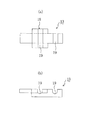
図7(a),(b)に示すように、上記各実施形態において、リード13の内部に広幅部18を設けることができる。ここで、リード13の2つの溝19のうち一方の溝19は幅の狭い部分にあり、他方の溝19は内方の広幅部18にあるようにする。このように、リード13の封止樹脂15内における内部側の幅が外側の幅より広くなるように厚さ方向の幅を加工することによリ、外部電極と封止樹脂との接着力を強化することができる。特に、リード13を側方に引っ張る力に対する広幅部18のアンカー効果によって、リード13の抜け,剥がれを防止することができ、半導体装置の信頼性の向上を図ることができる。
As shown in FIGS. 7A and 7B, in each of the above embodiments, the
さらに、リードの広幅部18において、図7(a)の破線に示すように、リード13の下部である外部電極16となる部分の幅を狭くすることにより、リード13に下方の引っ張り力に対するアンカー効果を生ぜしめることができ、外部電極16を下方にの引っ張る力に対する抜け,剥がれの防止に有効であり、半導体装置の信頼性の向上を図ることができる。
Further, in the
ただし、広幅部だけでなく狭幅部分にこのような段付形状が設けられていてもよいし、広幅部を有しない平面的にストレート形状のリードに対して段付形状が設けられていてもよい。 However, such a stepped shape may be provided not only at the wide portion but also at the narrow portion, or a stepped shape may be provided with respect to a planar straight lead having no wide portion. Good.
また、上記図1及び図2に示すような溝19を有しないリードに対しての本発明は適用できるものである。
Further, the present invention can be applied to a lead having no
なお、上記第2,第3の実施形態では、各外部電極16の配列ピッチが均一であっても、外部電極16の下面の面積が辺の中央部で小さくコーナー部で大きくすることにより、半導体装置の外部電極16とプリント配線板等の接続端子との接合の信頼性を高める効果があるのはいうまでもない。
In the second and third embodiments, even when the arrangement pitch of the
また、上記各実施形態では、吊りリードやダイパッドが存在するが、吊りリード,ダイパッドは必ずしも必要でない。吊りリードやダイパッドが存在しない半導体装置であっても、本発明の効果を有効に発揮することができる。 In each of the above embodiments, there are suspension leads and die pads, but the suspension leads and die pads are not necessarily required. Even in a semiconductor device in which no suspension lead or die pad exists, the effects of the present invention can be effectively exhibited.
さらに、上記各実施形態では、リードと半導体チップの電極パッドとを電気的に接続する接続部材として金属細線を用いているが、金属細線の代わりに、バンプ等を用いてもよいことはいうまでもない。 Furthermore, in each of the above embodiments, a metal thin wire is used as a connection member that electrically connects the lead and the electrode pad of the semiconductor chip. However, it goes without saying that a bump or the like may be used instead of the metal thin wire. Nor.
11 ダイパッド
12 半導体チップ
13 リード
14 金属細線(接続部材)
15 封止樹脂
16 外部電極
17 段差部
18 幅広部
19 溝
20 外枠
11
15
Claims (9)
溝を有するリードと、
前記ダイパッドに搭載された半導体チップと、
前記半導体チップと前記リードとを電気的に接続する金属細線と、
前記溝と、前記金属細線と、前記半導体チップと、前記リードの上面とを封止し、かつ、前記リードの下面の一部を露出する封止樹脂とを備え、
前記溝は、前記リードの下面の露出部の上方に位置し、
前記リードは、上方の幅が下方の幅よりも広い部分を有し、
前記金属細線は、前記リードの前記溝の上でない部分であって、前記封止樹脂に封止された部分に接続される樹脂封止型半導体装置。 Die pad,
A lead having a groove;
A semiconductor chip mounted on the die pad;
A fine metal wire for electrically connecting the semiconductor chip and the lead;
With said groove, said thin metal wire, and the semiconductor chip, sealing an upper surface of the lead, One or, a sealing resin for exposing a part of the lower surface of the front Symbol lead,
The groove is located above the exposed portion of the lower surface of the lead ,
The lead has a portion whose upper width is wider than the lower width;
The thin metal wire is a resin-encapsulated semiconductor device connected to a portion of the lead that is not above the groove and sealed with the sealing resin.
Priority Applications (1)
| Application Number | Priority Date | Filing Date | Title |
|---|---|---|---|
| JP2004240416A JP3639302B2 (en) | 2004-08-20 | 2004-08-20 | Resin-sealed semiconductor device |
Applications Claiming Priority (1)
| Application Number | Priority Date | Filing Date | Title |
|---|---|---|---|
| JP2004240416A JP3639302B2 (en) | 2004-08-20 | 2004-08-20 | Resin-sealed semiconductor device |
Related Parent Applications (1)
| Application Number | Title | Priority Date | Filing Date |
|---|---|---|---|
| JP1649898A Division JPH11214606A (en) | 1998-01-29 | 1998-01-29 | Resin molded semiconductor device and lead frame |
Publications (2)
| Publication Number | Publication Date |
|---|---|
| JP2004328015A JP2004328015A (en) | 2004-11-18 |
| JP3639302B2 true JP3639302B2 (en) | 2005-04-20 |
Family
ID=33509492
Family Applications (1)
| Application Number | Title | Priority Date | Filing Date |
|---|---|---|---|
| JP2004240416A Expired - Lifetime JP3639302B2 (en) | 2004-08-20 | 2004-08-20 | Resin-sealed semiconductor device |
Country Status (1)
| Country | Link |
|---|---|
| JP (1) | JP3639302B2 (en) |
Families Citing this family (5)
| Publication number | Priority date | Publication date | Assignee | Title |
|---|---|---|---|---|
| JP5183572B2 (en) * | 2009-06-08 | 2013-04-17 | 株式会社三井ハイテック | Lead frame and semiconductor device |
| JP5255009B2 (en) | 2010-02-26 | 2013-08-07 | ルネサスエレクトロニクス株式会社 | Semiconductor device |
| JP6253531B2 (en) | 2014-06-30 | 2017-12-27 | ルネサスエレクトロニクス株式会社 | Semiconductor device |
| CN111602240B (en) * | 2018-03-02 | 2023-08-01 | 新电元工业株式会社 | Resin-encapsulated semiconductor device |
| CN116613132A (en) * | 2023-07-19 | 2023-08-18 | 青岛泰睿思微电子有限公司 | Radio frequency chip packaging structure and method |
-
2004
- 2004-08-20 JP JP2004240416A patent/JP3639302B2/en not_active Expired - Lifetime
Also Published As
| Publication number | Publication date |
|---|---|
| JP2004328015A (en) | 2004-11-18 |
Similar Documents
| Publication | Publication Date | Title |
|---|---|---|
| US9171761B2 (en) | Resin sealing type semiconductor device and method of manufacturing the same, and lead frame | |
| JP4091050B2 (en) | Manufacturing method of semiconductor device | |
| US6753599B2 (en) | Semiconductor package and mounting structure on substrate thereof and stack structure thereof | |
| JP2000188366A (en) | Semiconductor device | |
| JP3470111B2 (en) | Method for manufacturing resin-encapsulated semiconductor device | |
| US20090020859A1 (en) | Quad flat package with exposed common electrode bars | |
| JPH11214606A (en) | Resin molded semiconductor device and lead frame | |
| JP2000091488A (en) | Resin-sealed semiconductor device and circuit member used therein | |
| JP3639302B2 (en) | Resin-sealed semiconductor device | |
| JP2569400B2 (en) | Method for manufacturing resin-encapsulated semiconductor device | |
| JP3502377B2 (en) | Lead frame, resin-encapsulated semiconductor device and method of manufacturing the same | |
| JPH09116045A (en) | Resin-sealed semiconductor device of bga type using lead frame and its manufacture | |
| KR100340862B1 (en) | Stack package and its manufacturing method | |
| JP2001077285A (en) | Lead frame and manufacture of resin-sealed semiconductor device using the same | |
| KR100668932B1 (en) | Leadframe and semiconductor package using it | |
| JP3271500B2 (en) | Semiconductor device | |
| JP2003007954A (en) | Manufacturing method for resin-sealing semiconductor device | |
| JP2007080889A (en) | Semiconductor device | |
| JP2000332146A (en) | Resin-sealed semiconductor device, circuit material usable therefor and manufacture thereof | |
| JP3361917B2 (en) | Lead frame, semiconductor device, and method of manufacturing semiconductor device | |
| JP6923299B2 (en) | Semiconductor devices and methods for manufacturing semiconductor devices | |
| JPH1126643A (en) | Semiconductor device | |
| KR200159861Y1 (en) | Semiconductor package | |
| KR100321149B1 (en) | chip size package | |
| JP2000277677A (en) | Lead frame, semiconductor package and manufacture thereof |
Legal Events
| Date | Code | Title | Description |
|---|---|---|---|
| A521 | Written amendment |
Free format text: JAPANESE INTERMEDIATE CODE: A523 Effective date: 20040826 |
|
| A621 | Written request for application examination |
Free format text: JAPANESE INTERMEDIATE CODE: A621 Effective date: 20040826 |
|
| A871 | Explanation of circumstances concerning accelerated examination |
Free format text: JAPANESE INTERMEDIATE CODE: A871 Effective date: 20040826 |
|
| A975 | Report on accelerated examination |
Free format text: JAPANESE INTERMEDIATE CODE: A971005 Effective date: 20040922 |
|
| A131 | Notification of reasons for refusal |
Free format text: JAPANESE INTERMEDIATE CODE: A131 Effective date: 20041005 |
|
| A521 | Written amendment |
Free format text: JAPANESE INTERMEDIATE CODE: A523 Effective date: 20041206 |
|
| TRDD | Decision of grant or rejection written | ||
| A01 | Written decision to grant a patent or to grant a registration (utility model) |
Free format text: JAPANESE INTERMEDIATE CODE: A01 Effective date: 20050105 |
|
| A61 | First payment of annual fees (during grant procedure) |
Free format text: JAPANESE INTERMEDIATE CODE: A61 Effective date: 20050113 |
|
| R150 | Certificate of patent or registration of utility model |
Free format text: JAPANESE INTERMEDIATE CODE: R150 |
|
| FPAY | Renewal fee payment (event date is renewal date of database) |
Free format text: PAYMENT UNTIL: 20080121 Year of fee payment: 3 |
|
| FPAY | Renewal fee payment (event date is renewal date of database) |
Free format text: PAYMENT UNTIL: 20090121 Year of fee payment: 4 |
|
| FPAY | Renewal fee payment (event date is renewal date of database) |
Free format text: PAYMENT UNTIL: 20090121 Year of fee payment: 4 |
|
| FPAY | Renewal fee payment (event date is renewal date of database) |
Free format text: PAYMENT UNTIL: 20100121 Year of fee payment: 5 |
|
| FPAY | Renewal fee payment (event date is renewal date of database) |
Free format text: PAYMENT UNTIL: 20110121 Year of fee payment: 6 |
|
| FPAY | Renewal fee payment (event date is renewal date of database) |
Free format text: PAYMENT UNTIL: 20110121 Year of fee payment: 6 |
|
| FPAY | Renewal fee payment (event date is renewal date of database) |
Free format text: PAYMENT UNTIL: 20120121 Year of fee payment: 7 |
|
| FPAY | Renewal fee payment (event date is renewal date of database) |
Free format text: PAYMENT UNTIL: 20130121 Year of fee payment: 8 |
|
| FPAY | Renewal fee payment (event date is renewal date of database) |
Free format text: PAYMENT UNTIL: 20130121 Year of fee payment: 8 |
|
| EXPY | Cancellation because of completion of term |