JP3628334B2 - Tuning amplifier - Google Patents
Tuning amplifier Download PDFInfo
- Publication number
- JP3628334B2 JP3628334B2 JP51804497A JP51804497A JP3628334B2 JP 3628334 B2 JP3628334 B2 JP 3628334B2 JP 51804497 A JP51804497 A JP 51804497A JP 51804497 A JP51804497 A JP 51804497A JP 3628334 B2 JP3628334 B2 JP 3628334B2
- Authority
- JP
- Japan
- Prior art keywords
- phase shift
- circuit
- resistor
- signal
- input
- Prior art date
- Legal status (The legal status is an assumption and is not a legal conclusion. Google has not performed a legal analysis and makes no representation as to the accuracy of the status listed.)
- Expired - Fee Related
Links
- 230000010363 phase shift Effects 0.000 claims description 275
- 239000003990 capacitor Substances 0.000 claims description 45
- 239000004065 semiconductor Substances 0.000 claims description 6
- 239000000758 substrate Substances 0.000 claims description 6
- 238000010586 diagram Methods 0.000 description 33
- 230000002452 interceptive effect Effects 0.000 description 5
- 230000003321 amplification Effects 0.000 description 4
- 238000003199 nucleic acid amplification method Methods 0.000 description 4
- 230000010354 integration Effects 0.000 description 2
- 230000002238 attenuated effect Effects 0.000 description 1
- 230000000903 blocking effect Effects 0.000 description 1
- 238000006243 chemical reaction Methods 0.000 description 1
- 239000000470 constituent Substances 0.000 description 1
- 230000000694 effects Effects 0.000 description 1
- 230000005669 field effect Effects 0.000 description 1
- 238000004519 manufacturing process Methods 0.000 description 1
- 238000000034 method Methods 0.000 description 1
- 238000012986 modification Methods 0.000 description 1
- 230000004048 modification Effects 0.000 description 1
- 230000010355 oscillation Effects 0.000 description 1
- 238000011144 upstream manufacturing Methods 0.000 description 1
Images
Classifications
-
- H—ELECTRICITY
- H03—ELECTRONIC CIRCUITRY
- H03H—IMPEDANCE NETWORKS, e.g. RESONANT CIRCUITS; RESONATORS
- H03H11/00—Networks using active elements
- H03H11/02—Multiple-port networks
- H03H11/16—Networks for phase shifting
- H03H11/20—Two-port phase shifters providing an adjustable phase shift
-
- H—ELECTRICITY
- H03—ELECTRONIC CIRCUITRY
- H03F—AMPLIFIERS
- H03F3/00—Amplifiers with only discharge tubes or only semiconductor devices as amplifying elements
- H03F3/189—High-frequency amplifiers, e.g. radio frequency amplifiers
- H03F3/19—High-frequency amplifiers, e.g. radio frequency amplifiers with semiconductor devices only
- H03F3/191—Tuned amplifiers
-
- H—ELECTRICITY
- H03—ELECTRONIC CIRCUITRY
- H03F—AMPLIFIERS
- H03F3/00—Amplifiers with only discharge tubes or only semiconductor devices as amplifying elements
- H03F3/189—High-frequency amplifiers, e.g. radio frequency amplifiers
- H03F3/19—High-frequency amplifiers, e.g. radio frequency amplifiers with semiconductor devices only
- H03F3/195—High-frequency amplifiers, e.g. radio frequency amplifiers with semiconductor devices only in integrated circuits
-
- H—ELECTRICITY
- H03—ELECTRONIC CIRCUITRY
- H03H—IMPEDANCE NETWORKS, e.g. RESONANT CIRCUITS; RESONATORS
- H03H11/00—Networks using active elements
- H03H11/02—Multiple-port networks
- H03H11/04—Frequency selective two-port networks
- H03H11/12—Frequency selective two-port networks using amplifiers with feedback
- H03H11/1217—Frequency selective two-port networks using amplifiers with feedback using a plurality of operational amplifiers
Landscapes
- Engineering & Computer Science (AREA)
- Power Engineering (AREA)
- Microelectronics & Electronic Packaging (AREA)
- Amplifiers (AREA)
- Networks Using Active Elements (AREA)
Description
技術分野
この発明は、集積化が容易な同調増幅器に関し、特に、同調周波数と最大減衰量とを互いに干渉することなく、任意に調整し得る同調増幅器に関する。
背景技術
従来から、能動素子およびリアクタンス素子を使用した各種の同調増幅器が提案され実用化されている。
例えばLC共振を利用した従来の同調増幅器は、同調周波数を調整するとLC回路に依存するQと利得が変化し、最大減衰量を調整すると同調周波数が変化し、最大減衰量を調整すると同調周波数における利得が変化するという特徴を有する。したがって、従来の同調増幅器においては、同調周波数、同調周波数における利得、最大減衰量C1、C2を互いに干渉しあうことなく調整することは極めて困難であった。また、同調周波数および最大減衰量を調整し得る同調増幅器を集積回路によって形成することは困難であった。
本発明は、このような点に鑑みて創作されたものであり、その目的は集積化に適しており、同調周波数、同調周波数における利得、最大減衰量を互いに干渉しあうことなく調整することができ、特に同調周波数を可変したときに出力振幅の変化を抑えることができる同調増幅器を提供することにある。
発明の開示
本発明はこのような課題を解決するために考えられたものであり、同調周波数、同調周波数における利得、最大減衰量を互いに干渉させることなく調整することができ、特に同調周波数を可変したときに出力振幅の変化を抑えることができる同調増幅器を提供することにある。
本発明の同調増幅器は、出力が入力側に帰還された差動増幅器を含む全域通過型の2つの移相回路と、
前記2つの移相回路のそれぞれを縦続接続して形成される帰還ループの一部に挿入される分圧回路とを備え、
前記縦続接続された2つの移相回路のうち前段の移相回路に対して前記加算回路によって加算された信号を入力するとともに、後段の移相回路から出力された信号を前記帰還信号として前記加算回路に入力し、前記分圧回路に入力される交流信号を前記同調信号として出力する。
また、本発明の同調増幅器は、入力信号が一方端に入力される入力インピーダンス素子と、帰還信号が一方端に入力される帰還インピーダンス素子とを含んでおり、前記入力信号と前記帰還信号とを加算する加算回路と、
反転入力端子に第1の抵抗の一方端が接続され前記第1の抵抗を介して交流信号が入力される差動増幅器と、前記差動増幅器の出力端子に接続された第1の分圧回路と、前記第1の分圧回路の出力端と前記差動増幅器の反転入力端子との間に接続された第2の抵抗と、キャパシタあるいはインダクタによるリアクタンス素子と第3の抵抗とで構成され前記第1の抵抗の他方端に接続された直列回路とを含み、前記第3の抵抗および前記リアクタンス素子の接続部を前記差動増幅器の非反転入力端子に接続した2つの移相回路と、
を備え、前記2つの移相回路のそれぞれを縦続接続し、これら縦続接続された2つの移相回路のうち前段の移相回路に対して前記加算回路によって加算された信号を入力するとともに、後段の移相回路から出力された信号を前記帰還信号として前記帰還インピーダンス素子の一方端に入力し、これら2つの移相回路のいずれかの出力を同調信号として出力する。
また、本発明の同調増幅器は、入力信号が一方端に入力される入力インピーダンス素子と、帰還信号が一方端に入力される帰還インピーダンス素子とを含んでおり、前記入力信号と前記帰還信号とを加算する加算回路と、
反転入力端子の第1の抵抗の一方端が接続され前記第1の抵抗を介して交流信号が入力される差動増幅器と、前記差動増幅器の反転入力端子と出力端子との間に接続された第2の抵抗と、一方端が前記差動増幅器の反転入力端子に接続され他方端が接地された第3の抵抗と、キャパシタあるいはインダクタによるリアクタンス素子と第4の抵抗とで構成され前記第1の抵抗の他方端に接続された直列回路とを含み、前記第4の抵抗および前記リアクタンス素子の接続部を前記差動増幅器の非反転入力端子に接続した2つの移相回路と、
を備え、前記2つの移相回路のそれぞれを縦続接続し、これら縦続接続された2つの移相回路のうち前段の移相回路に対して前記加算回路によって加算された信号を入力するとともに、後段の移相回路から出力された信号を前記帰還信号として前記帰還インピーダンス素子の一方端に入力し、これら2つの移相回路のいずれかの出力を同調信号として出力する。
また、本発明の同調増幅器は、入力信号が一方端に入力される入力インピーダンス素子と、帰還信号が一方端に入力される帰還インピーダンス素子とを含んでおり、前記入力信号と前記帰還信号とを加算する加算回路と、
反転入力端子に第1の抵抗の一方端が接続され前記第1の抵抗を介して交流信号が入力される差動増幅器と、前記差動増幅器の出力端子に接続された第1の分圧回路と、前記第1の分圧回路の出力端と前記差動増幅器の反転入力端子との間に接続された第2の抵抗と、キャパシタあるいはインダクタによるリアクタンス素子と第3の抵抗とで構成され前記第1の抵抗の他方端に接続された直列回路とを含み、前記第3の抵抗および前記リアクタンス素子の接続部を前記差動増幅器の非反転入力端子に接続した第1の移相回路と、
反転入力端子に第4の抵抗の一方端が接続され前記第4の抵抗を介して交流信号が入力される差動増幅器と、前記差動増幅器の反転入力端子と出力端子との間に接続された第5の抵抗と、一方端が前記差動増幅器の反転入力端子に接続され他方端が接地された第6の抵抗と、キャパシタあるいはインダクタによるリアクタンス素子と第7の抵抗とで構成され前記第4の抵抗の他方端に接続された直列回路とを含み、前記第7の抵抗および前記リアクタンス素子の接続部を前記差動増幅器の非反転入力端子に接続した第2の移相回路と、
を備え、前記第1および第2の移相回路を縦続接続し、これら縦続接続された2つの移相回路のうち前段の移相回路に対して前記加算回路によって加算された信号を入力するとともに、後段の移相回路から出力された信号を前記帰還信号として前記帰還インピーダンス素子の一方端に入力し、前記第1および第2の移相回路のいずれかの出力を前記同調信号として出力する。
【図面の簡単な説明】
第1図は、本発明を適用した第1の実施形態の同調増幅器の構成を示す回路図、
第2図は、第1図に示した前段の移相回路の構成を抜き出して示した図、
第3図は、前段の移相回路の入出力電圧とキャパシタ等に現れる電圧との関係を示すベクトル図、
第4図は、第1図に示した後段の移相回路の構成を抜き出して示した図、
第5図は、後段の移相回路の入出力電圧とキャパシタ等に現れる電圧との関係を示すベクトル図、
第6図は、上述した構成を有する2つの移相回路および分圧回路の全体を伝達関数K1を有する回路に置き換えたシステム図、
第7図は、第6図に示すシステムをミラーの定理によって交換したシステム図、
第8図は、第1図に示した同調増幅器の同調特性を示す図、
第9図は、LR回路を含む移相回路の構成を示す回路図、
第10図は、第9図に示した移相回路の入出力電圧とインダクタ等に現れる電圧との関係を示すベクトル図、
第11図は、LR回路を含む他の移相回路の構成を示す回路図、
第12図は、第11図に示した移相回路の入出力電圧とインダクタ等に現れる電圧との関係を示すベクトル図、
第13図は、同調増幅器の第3の実施態様を示す回路図、
第14図は、第13図に示した移相回路を一般化した図、
第15図は、第13図に示した同調増幅器の前段の移相回路と置き換え可能な移相回路の構成を示す回路図、
第16図は、第13図に示した同調増幅器の後段の移相回路と置き換え可能な移相回路の構成を示す回路図、
第17図は、同調増幅器の第5の実施形態の構成を示す回路図、
第18図は、オペアンプの構成の中で本発明の移相回路の動作に必要な部分を押出した回路図である。
発明を実施するための最良の形態
〔同調増幅器の第1の実施形態〕
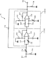
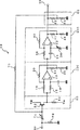
第1図は、本発明を適用した第1の実施形態の同調増幅器の構成を示す回路図である。
同図に示す同調増幅器1は、それぞれが入力される交流信号の位相を所定量シフトさせることにより所定の周波数において合計で360゜の位相シフトを行う2つの移相回路10C、30Cと、後段の移相回路30Cの出力側に設けられた抵抗62および64からなる分圧回路60と、帰還抵抗70および入力抵抗74(入力抵抗74は帰還抵抗70の抵抗値のn倍の抵抗値を有しているものとする)のそれぞれを介することにより分圧回路60の分圧出力(帰還信号)と入力端子90に入力される信号(入力信号)とを所定の割合で加算する加算回路とを含んで構成されている。
第2図は、第1図に示した前段の移相回路10Cの構成を抜き出して示したものである。同図に示す移相回路10Cは、入力端24に入力された交流信号の位相を所定量シフトさせてオペアンプ12の非反転入力端子に入力する可変抵抗16およびキャパシタ14と、入力端24とオペアンプ12の反転入力端子との間に挿入された抵抗18と、オペアンプ12の出力端子に接続されて分圧回路を構成する抵抗21および23と、この分圧回路とオペアンプ12の反転入力端子との間に接続された抵抗20とを含んで構成されている。
このような構成を有する移相回路10Cにおいて、抵抗18と抵抗20の抵抗値は同じに設定されている。
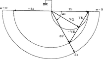
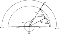
第2図に示す入力端24に所定の交流信号が入力されると、オペアンプ12の非反転入力端子には、キャパシタ14の両端に現れる電圧VC1が印加される。また、抵抗18の両端には、可変抵抗16の両端に現れる電圧VR1と同じ電圧VR1が現れる。2つの抵抗18、20には同じ電流Iが流れ、しかも、上述したように抵抗18と抵抗20の各抵抗値が等しいので、抵抗20の両端にも電圧VR1が現れる。オペアンプ12の反転入力端子(電圧VC1)を基準にして考えると、抵抗18の両端電圧VR1をベクトル的に加算したものが入力電圧Eiに、抵抗20の両端電圧VR1をベクトル的に減算したものが抵抗21と抵抗23の接続点の電圧(分圧出力)Eo′になる。
第3図は、前段の移相回路10Cの入出力電圧とキャパシタ等に現れる電圧との関係を示すベクトル図である。
上述したように、オペアンプ12の非反転入力端子に印加される電圧VC1を基準に考えると、入力電圧Eiと分圧電圧Eo′とは電圧VR1を合成する方向が異なるだけでありその絶対値は等しくなる。したがって、入力電圧Eiと分圧出力Eo′の大きさと位相の関係は、入力電圧Eiおよび分圧出力Eo′を斜辺とし、電圧VR1の2倍を底辺とする二等辺三角形で表すことができ、分圧出力Eo′の振幅は周波数に関係なく入力信号の振幅と同じであって、位相シフト量は第3図に示すφ1で表されることがわかる。この位相のシフト量φ1は、周波数に応じて0゜から180゜まで変化する。しかも、可変抵抗16の抵抗値Rを可変することにより、位相シフト量φ1は変化する。
また、移相回路10Cの出力端26はオペアンプ12の出力端子に接続されているため、抵抗21の抵抗値をR21、抵抗23の抵抗値をR23とすると、出力電圧Eoと上述した分圧出力Eo′との間には、抵抗20の抵抗値に対してR21、R23が十分小さいときはEo=(1+R21/R23)Eo′の関係がある。したがって、R21およびR23の値を調整することにより1より大きな利得が得られ、しかも第3図に示すように周波数が変化しても出力電圧Eoの振幅が一定であり、位相のみを所定量シフトすることができる。
同様に、第4図は第1図に示した後段の移相回路30Cの構成を抜き出して示したものである。同図に示す後段の移相回路30Cは、差動増幅器の一種であるオペアンプ32と、入力端44に入力された信号の位相を所定量シフトさせてオペアンプ32の非反転入力端子に入力するキャパシタ34および可変抵抗36と、入力端44とオペアンプ32の反転入力端子との間に挿入された抵抗38と、オペアンプ32の出力端子に接続されて分圧回路を構成する抵抗41および43と、この分圧回路とオペアンプ32の反転入力端子との間に接続された抵抗40とを含んで構成されている。
このような構成を有する移相回路30Cにおいて、抵抗38と抵抗40の抵抗値は同じに設定されている。
第4図に示した入力端44に所定の交流信号が入力されると、オペアンプ32の非反転入力端子には、可変抵抗36の両端に現れる電圧VR2が印加される。また、抵抗38の両端には、キャパシタ34の両端に現れる電圧VC2と同じ電圧VC2が現れる。2つの抵抗38、40には同じ電流Iが流れ、しかも、上述したように抵抗38と抵抗40の各抵抗値が等しいので、抵抗40の両端にも電圧VC2が現れる。オペアンプ32の反転入力端子(電圧VR2)を基準にして考えると、抵抗38の両端電圧VC2をベクトル的に加算したものが入力電圧Eiに、抵抗40の両端電圧VC2をベクトル的に減算したものが抵抗41と抵抗43の接続点の電圧(分圧出力)Eo′になる。
第5図は、後段の移相回路30Cの入出力電圧とキャパシタ等に現れる電圧との関係を示すベクトル図である。
上述したように、オペアンプ32の非反転入力端子に印加される電圧VR2を基準に考えると、入力電圧Eiと分圧出力Eo′とは電圧VC2を合成する方向が異なるだけでありその絶対値は等しくなる。したがって、入力電圧Eiと分圧出力Eo′の大きさと位相の関係は、入力電圧Eiおよび分圧出力Eo′を斜辺とし、電圧VC2の2倍を底辺とする二等辺三角形で表すことができ、分圧出力Eo′の振幅は周波数に関係なく入力信号の振幅と同じであって、位相シフト量は第5図に示すφ2で表されることがわかる。この位相シフト量φ2は、周波数に応じて、入力電圧Eiを基準として時計回り方向(位相遅れ方向)に180゜から360゜まで変化する。しかも、可変抵抗36の抵抗値Rを可変することにより、位相シフト量φ2は変化する。
また、移相回路30Cの出力端46はオペアンプ32の出力端子に接続されているため、抵抗41の抵抗値をR41、抵抗43の抵抗値をR43とすると、出力電圧Eoと上述した分圧出力Eo′との間には、抵抗40の抵抗値に対してR41、R43が十分小さいときはEo=(1+R41/R43)Eo′の関係がある。したがって、R41およびR43の値を調整することにより1より大きな利得が得られ、しかも第5図に示すように周波数が変化しても出力電圧Eoの振幅が一定であり、位相のみを所定量シフトすることができる。
このようにして、2つの移相回路10C、30Cのそれぞれにおいて位相が所定量シフトされ、第3図および第5図に示すように、所定の周波数において2つの移相回路10C、30Cの全体により位相シフト量の合計が360゜となる。
また、後段の移相回路30Cの出力は、出力端子92から同調増幅器1の出力として取り出されるとともに、この移相回路30Cの出力を分圧回路60を通した信号が帰還抵抗70を介して前段の移相回路10Cの入力側に帰還されている。そして、この帰還された信号と入力抵抗74を介して入力される信号とが加算され、この加算された信号が前段の移相回路10Cに入力される。
このように、2つの移相回路10C、30Cによって所定の周波数における位相シフト量の合計が360゜となり、このとき2つの移相回路10C、30C、分圧回路60および帰還抵抗70を含んで形成される帰還ループのループゲインを1以下に設定することにより、上述した所定の周波数成分の信号のみを通過させる同調動作が行われる。
また、同調増幅器1の出力端子92からは、分圧回路60に入力される前の移相回路30Cの出力が取り出されているため、同調増幅器1自体に利得を持たせることができ、同調動作と同時に信号振幅の増加が可能となる。
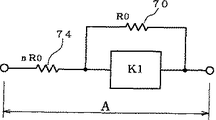
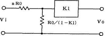
第6図は、上述した構成を有する2つの移相回路10C、30Cおよび分圧回路60の全体を伝達関数K1を有する回路に置き換えたシステム図であり、伝達関数K1を有する回路と並列に抵抗R0を有する帰還抵抗70が、直列に帰還抵抗70のn倍の抵抗値(nR0)を有する入力抵抗74が接続されている。
第7図は、第6図に示すシステムをミラーの定理によって変換したシステム図であり、変換後のシステム全体の伝達関数Aは、
A=Vo/Vi=K1/{n(1−K1)+1} ・・・(1)
で表すことができる。
前段の移相回路10Cの伝達関数K2は、可変抵抗16とキャパシタ14からなるCR回路の時定数をT1(可変抵抗16の抵抗値をR、キャパシタ14の静電容量をCとするとT1=CR)とすると、
K2=a1(1−T1s)/(1+T1s) ・・・(2)
となる。ここで、s=jωであり、a1は移相回路10Cの利得であって、a1=(1+R21/R23)>1である。
また、後段の移相回路30Cの伝達関数K3は、キャパシタ34と可変抵抗36からなるCR回路の時定数をT2(キャパシタ34の静電容量をC、可変抵抗36の抵抗値をRとするとT2=CR)とすると、
K3=−a2(1−T2s)/(1+T2s) ・・・(3)
となる。ここで、a2は移相回路30Cの利得であってa2=(1+R41/R43)>1である。
分圧回路60を介することによって信号振幅が1/a1a2に減衰するものとすると、2つの移相回路10C、30Cと分圧回路60を縦続接続した場合の全体の伝達関数K1は、
K1=−{1+(Ts)2−2Ts}/{1+(Ts)2+2Ts} ・・・(4)
となる。なお、上述した(4)式においては、計算を簡単なものとするために、各移相回路の時定数T1、T2をともにTとした。この(4)式を上述した(1)式に代入すると、
A=−{1+(Ts)2−2Ts}
/〔(2n+1){1+(Ts)2}+2Ts〕
=−{1/(2n+1)}〔{1+(Ts)2−2Ts}
/{1+(Ts)2+2Ts/(2n+1)}〕 ・・・(5)
となる。
この(5)式によれば、ω=0(直流の領域)のときにA=−1/(2n+1)となって、最大減衰量を与えることがわかる。また、ω=∞のときにもA=−1/(2n+1)となって、最大減衰量を与えることがわかる。さらに、ω=1/Tの同調点(各移相回路の時定数が異なる場合には、
![]()
ところで、上述した第6図において、伝達関数K1で示される全域通過回路が入力インピーダンスを有する場合、帰還抵抗70とこの全域通過回路の入力インピーダンスによる分圧回路が形成されるため、全域通過回路を含む帰還ループのオープンループゲインは伝達関数K1の絶対値より小さくなる。全域通過回路の入力インピーダンスとは、前段の移相回路10Cの入力インピーダンスであり、オペアンプ12の入力抵抗18に可変抵抗16とキャパシタ14からなるCR回路の直列インピーダンスが並列に接続されて形成される入力インピーダンスに他ならない。したがって、全域通過回路の入力インピーダンスによる帰還ループのオープンループゲインの損失を補償するには、全域通過回路自体の利得を1以上に設定することが必要である。
例えば、移相回路10Cに含まれる抵抗21、23による分圧回路を無視して考える(分圧比が1の場合であって、上述した(2)式におけるa1が1の場合を考える)と、移相回路10Cは、(2)式によれば、入力された周波数に応じて利得が1倍のホロワ回路から利得が−1倍の反転増幅器としての範囲で動作しなければならないので、抵抗18と20の抵抗比を1以外にすることは好ましくない。なぜなら、抵抗18、20の各抵抗値をR18、R20とすると、移相回路10Cが反転増幅器として動作するときの利得は−R20/R18であるが、ホロワ回路として動作する場合の利得は抵抗18と抵抗20の抵抗比にかかわらず常に1であるから、抵抗18と抵抗20の抵抗比が1でない場合には、移相回路10Cが動作する全領域において、その入出力間の位相だけが変化し、出力振幅が変化しない理想条件が満足できなくなるからである。
移相回路10Cの出力側に抵抗21と抵抗23からなる分圧回路を付加し、この分圧回路を介してオペアンプ12の反転入力端子への帰還を施すことにより、抵抗18と抵抗20の抵抗比を1に保持したまま移相回路10Cの利得を1以上に設定することが可能となる。同様に、移相回路30Cの出力側に抵抗41と抵抗43からなる分圧回路を付加し、この分圧回路を介してオペアンプ32の反転入力端子への帰還を施すことにより、抵抗38と抵抗40の抵抗比を1に保持したまま移相回路30Cの利得を1以上に設定することが可能となる。
なお、上述したように、移相回路10C内の可変抵抗16と移相回路30C内の可変抵抗36の抵抗値を変えることにより、キャパシタ14および可変抵抗16からなるCR回路の時定数T1と、キャパシタ34および可変抵抗36からなるCR回路の時定数T2とを変化させることができるため、
![]()
また、(2)式あるいは(3)式から第3図、第5図に示したφ1、φ2を求めると、
φ1=tan{2ωT1/(1−ω2T1 2)} ・・・(6)
φ2=tan{2ωT2/(1−ω2T2 2)} ・・・(7)
となる。なお、(6)、(7)式のφ1およびφ2は、第3図および第5図に示す入力電圧Eiを基準として時計回り方向(位相遅れ方向)を正方向としたものである。
例えばT1=T2(=T)の場合には、ω=1/Tのときに2つの移相回路10C、30Cによる位相シフト量の合計が360゜となって上述した同調動作が行われ、このときφ1=90゜、φ2=270゜となる。
このように、第1の実施形態の同調増幅器1は、帰還抵抗70と入力抵抗74の抵抗比nを変えても同調周波数および同調時の利得が一定で、かつ最大減衰量および同調帯域幅を変えることができる同調増幅器1を用いて同調動作を行っているため、混信が生じる場合には上述した抵抗比nを大きく設定して同調帯域幅を狭くして混信を防ぐことができ、反対に混信が少ない場合には上述した抵抗比nを小さく設定して同調帯域幅を広げて受信信号を忠実に再現することができる。
なお、上述した第1の実施形態では、帰還抵抗70と入力抵抗74の抵抗値を固定にしているが、少なくともいずれか一方の抵抗を可変できるようにして、上述した抵抗比nを任意に変更可能としてもよい。
また、第1の実施形態の同調増幅器1は、移相回路10C内の抵抗18と抵抗20の抵抗値を同じ値に設定するとともに移相回路30C内の抵抗38と抵抗40の抵抗値を同じ値に設定するため、同調周波数を変えても振幅が変動することはなく、ほぼ一定の振幅を有する同調出力を得ることができる。
特に、同調出力の振幅変動を抑えたことにより、上述した抵抗比nを大きくして同調増幅器1のQの値を大きくすることができる。すなわち、オープンループゲインに周波数依存性があると、利得の低い周波数では抵抗比nを大きくしてもQが上がらず、利得の高い周波数ではオープンループゲインが1を越えて発振することがある。したがって、振幅変動が大きい場合には、このような発振を防止するために抵抗比nをあまり大きな値に設定することができず、同調増幅器1のQの値も小さくなる。これに対して、上述した第1の実施形態では、移相回路10C、30C内にそれぞれ分圧回路を設け、かつ抵抗18と20、抵抗38と40の抵抗値をそれぞれ同じ値に設定することにより、同調増幅器1の同調出力の振幅変動を抑えるため、抵抗比nを大きく設定することができる、同調増幅器1のQの値を大きくすることができる。
また、分圧回路60を介して減衰した信号を帰還信号として用いるとともに、分圧回路60に入力する前の信号を同調増幅器1の出力として取り出すことにより、入力信号の中から所定の周波数成分のみを抽出する同調動作とともに、この抽出された信号に対する所定の増幅動作を行うことができる。しかも、このときの利得は、分圧回路60の分圧比を変えることにより任意に設定できる。
また、最大減衰量は、帰還抵抗70と入力抵抗74の抵抗比nによって決定され、同調周波数は可変抵抗16または36の抵抗値によって決定されるため、同調周波数や最大減衰量を互いに干渉しあうことなく調整することができる。なお、可変抵抗16,36のいずれか一方を抵抗値が固定の抵抗に置き換えてもよい。
さらに、上述した同調増幅器1は、オペアンプ、キャパシタおよび抵抗を組み合わせて構成しており、すべての構成素子を半導体基板上に形成することができる。
また、可変抵抗16、36の少なくとも一方の抵抗値を連続的に変えることにより、同調周波数を連続的に変更でき、同調周波数の変更のために従来は必要不可欠であったバリコンを省くことができる。したがって、製造工程が大幅に簡略化され、コストダウンも図れる。
なお、上述した第2図の移相回路10Cと第4図の移相回路30Cを縦続接続する場合には、各移相回路内のオペアンプ12あるいは32の出力端に接続された分圧回路のうち、いずれか一方の分圧回路を省略し、あるいは分圧比を1に設定してもよい。例えば、移相回路10C内の分圧回路を省略してオペアンプ12の出力端子を抵抗20の一方端に直接接続する。これは、分圧回路を構成する抵抗62の抵抗値を極端に小さな値にして、分圧比を1に設定したことと同じである。
このように、縦続接続された2つの移相回路の一方について分圧回路を省略してゲインを1に設定した場合には、他方の移相回路10Cのゲインを1より大きな値に設定することにより、第1図に示した同調増幅器1と同様の同調動作が行われる。
また、増幅動作が不要な場合には、移相回路30Cの後段の分圧回路60を省略し、移相回路30Cの出力を直接前段側に帰還してもよい。あるいは分圧回路60内の抵抗62の抵抗値を極端に小さな値にして分圧比を1に設定してもよい。
〔第2の実施形態〕
上述した同調増幅器1においては、CR回路を一部に含むように各移相回路10C、30Cを構成したが、CR回路の代わりにLR回路を一部に含むように移相回路を構成することもできる。
第9図は、LR回路を含む移相回路の構成を示す回路図であり、第1図に示した同調増幅器1の前段の移相回路10Cと置き換え可能な構成が示されている。同図に示す移相回路10Lは、第1図に示した前段の移相回路10C内のキャパシタ14と可変抵抗16からなるCR回路を、可変抵抗16とインダクタ17からなるLR回路に置き換えた構成を有しており、抵抗18と抵抗20の各抵抗値は同じ値に設定されている。
したがって、上述した移相回路10Lの入出力電圧等の関係は、第10図のベクトル図に示すように、第3図に示した電圧VC1を可変抵抗16の両端電圧VR3に、第3図に示した電圧VR1をインダクタ17の両端電圧VL1にそれぞれ置き換えて考えることができる。
また、第9図に示した移相回路10Lの伝達関数は、インダクタ17と可変抵抗16からなるLR回路の時定数をT1(インダクタ17のインダクタンスをL、可変抵抗16の抵抗値をRとするとT1=L/R)とすると、(2)式に示したK2をそのまま適用でき、第10図に示す位相シフト量φ3も上述した(6)式に示したφ1と同じになる。
このように、第9図に示す移相回路10Lは、第2図に示した移相回路10Cと基本的に等価であり、第1図に示した移相回路10Cから第9図に示した移相回路10Lへの置き換えが可能であることがわかる。また、第9図に示した抵抗18と20の各抵抗値は同じ値に設定されているため、同調周波数を可変した際の振幅変動がなく、ほぼ一定の同調出力を得ることができる。
第11図は、LR回路を含む移相回路の他の構成を示す回路図であり、第1図に示した同調増幅器1の後段の移相回路30Cと置き換え可能な構成が示されている。同図に示す移相回路30Lは、第4図に示した後段の移相回路30C内のキャパシタ34と可変抵抗36からなるCR回路を、可変抵抗36とインダクタ37からなるLR回路に置き換えた構成を有しており、抵抗38と抵抗40の各抵抗値は同じ値に設定されている。
したがって、上述した移相回路30Lの入出力電圧等の関係は、第12図のベクトル図に示すように、第5図に示した電圧VR2をインダクタ37の両端電圧VL2に、第5図に示した電圧VC2を可変抵抗36の両端電圧VR4にそれぞれ置き換えて考えることができる。
ところで、第11図に示した移相回路30Lの伝達関数は、可変抵抗36とインダクタ37からなるLR回路の時定数をT2(可変抵抗36の抵抗値をR、インダクタ37のインダクタンスをLとするとT2=L/R)とすると、(3)式に示したK3をそのまま適用でき、第12図に示す位相シフト量φ4も上述した(7)式に示したφ2と同じになる。
このように、第1図に示した2つの移相回路10Cおよび30Cのいずれか一方、あるいは両方を第9図、第11図に示した移相回路10L、30Lに置き換えることができる。2つの移相回路10C、30Cの両方を移相回路10L、30Lに置き換えた場合には、同調増幅器全体を集積化することにより同調周波数の高周波化が容易となる。
また、2つの移相回路10C、30Cのいずれか一方のみを移相回路10Lあるいは30Lに置き換えた場合であって、LR回路を構成するインダクタを含めて、あるいはこのインダクタを除く同調回路全体を集積化した場合には、温度変化による同調周波数の変動を防止する。いわゆる温度補償が可能となる。
なお、第1図に示した移相回路10C、30Cの少なくとも一方を、第9図あるいは第11図に示した移相回路10L、30Lに置き換えた場合には、各移相回路内のオペアンプ12あるいは32の出力端に接続された分圧回路のうち、いずれか一方の分圧回路を省略し、あるいは分圧比を1に設定してもよい。また、分圧回路60を構成する抵抗62の抵抗値を極端に小さな値にして、分圧比を1にしてもよい。
〔第3の実施形態〕
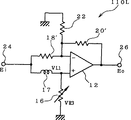
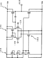
第13図は、同調増幅器の第3の実施形態を示す回路図である。同図に示す同調増幅器1Aは、それぞれが入力される交流信号の位相を所定量シフトさせることにより所定の周波数において合計で360゜の位相シフトを行う2つの移相回路110C、130Cと、帰還抵抗70および入力抵抗74(入力抵抗74は帰還抵抗70の抵抗値のn倍の抵抗値を有しているものとする)のそれぞれを介することにより後段の移相回路130Cの出力(帰還信号)と入力端子90に入力される信号(入力信号)とを所定の割合で加算する加算回路とを含んで構成されている。
第1図に示した同調増幅器1においては、前段の移相回路10C内の抵抗18と抵抗20の各抵抗値を同じに設定することで、入力される交流信号の周波数が変わったときの振幅変化を抑え、オペアンプ12の出力側に抵抗21と23による分圧回路を接続することで、移相回路10Cの利得を1より大きな値に設定している。これに対し、第13図に示す同調増幅器1Aに含まれる前段の移相回路110Cは、上述した抵抗21、23による分圧回路を用いずに、抵抗18′の抵抗値よりも抵抗20′の抵抗値を大きく設定することにより、移相回路110Cの利得を1より大きな値に設定している。
後段の移相回路130Cについても同様であり、抵抗38′の抵抗値よりも抵抗40′の抵抗値を大きく設定することで、移相回路130Cの利得を1より大きな値に設定している。また、移相回路130Cの出力端子には、帰還抵抗70、出力端子92および抵抗78が接続されている。
なお、第13図に示す同調増幅器1Aにおいては、後段の移相回路130Cのさらに後段に分圧回路を接続し、その分圧出力を帰還抵抗70を介して帰還させるようにしてもよい。
ところで、各移相回路の利得を1より大きな値に設定した場合には、入力される信号の周波数に応じて利得変動が生じる。例えば、前段の移相回路110Cについて考えると、入力信号の周波数が低い場合には移相回路110Cはボルテージホロワ回路となるためこのときの利得は1倍となるのに対し、周波数が高い場合には移相回路110Cは反転増幅器となるためこのときの利得は−m倍(mは抵抗20′と抵抗18′の抵抗比)となるため、入力信号の周波数が変化したときに移相回路110Cの利得も変化して出力信号の振幅変動が生じる。
このような振幅変動は、オペアンプ12の反転入力端子に抵抗22を接続して、入力信号の周波数が低い場合と高い場合の利得を一致させることにより抑えることができる。移相回路130Cについても同様であり、オペアンプ32の反転入力端子に所定の抵抗値を有する抵抗42を接続することにより、出力信号の振幅変動を抑えることができる。
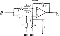
次に、この抵抗22(あるいは抵抗42)の抵抗値をどのような値に設定すればよいかを検討する。第14図は、上述した移相回路110Cおよび130Cを一般化した図であり、各移相回路に含まれるCR回路をインピーダンスz1、z2を有する素子に置き換えた構成が示されている。同図に示すように、オペアンプの入力抵抗の抵抗値をr、帰還抵抗の抵抗値をmr、オペアンプの反転入力端子に接続された抵抗(抵抗22あるいは42)の抵抗値をR、オペアンプの反転入力端子の電位をVとする。
入力電圧Eiと電圧Vとの間には、
r(I a+I b)+V=Ei ・・・(8)
の関係がある。また、電圧Vを第14図に示した各種の定数を用いて表すと、
V=I b R ・・・(9)
V=Eo+mr・I a ・・・(10)
V={z2/(z1+z2)}Ei=kEi ・・・(11)
となる。(11)式において、インピーダンスz1、z2を有する2つの素子による分圧比をkとした。
(10)式からI aを、(9)式からI bをそれぞれ求め、これらを(8)式に代入し、さらにその代入した結果に(11)式を代入してVを消去すると、
Eo=(Rk+Rmk+mrk−Rm)Ei/R ・・・(12)
となる。
ところで、第14図に示した移相回路が反転増幅器として動作する場合とは、インピーダンスz2が0Ωであってk=0の場合であり、このとき(12)式から、
Eo=−mEi ・・・(13)
となる。また、第14図に示した移相回路がホロワ回路として動作する場合とは、インピーダンスz1が0Ωであってk=1の場合であり、このとき(12)式から、
Eo=(R+mr)Ei/R ・・・(14)
となる。移相回路110Cあるいは130Cが反転増幅器およびホロワ回路として動作するときの利得変動がない場合とは、(13)式で求めたEoの絶対値と(14)式で求めたEoの絶対値が等しい場合であり、
m=(R+mr)/R ・・・(15)
となる。Rについて解くと、
R=mr/(m−1) ・・・(16)
となる。したがって、移相回路110C内の抵抗22の抵抗値R、あるいは移相回路130C内の抵抗42の抵抗値Rを(16)式に従って設定することにより、同調周波数を低周波から高周波まで変化させたときに生じる利得変動を抑えることができる。
〔第4の実施形態〕
第13図に示す同調増幅器1Aでは、移相回路110Cおよび130C内にCR回路を含む例を説明したが、CR回路の代わりにLR回路を含む場合にも、同様の移相回路を構成できる。
第15図は、LR回路を含む移相回路の構成を示す回路図であり、第13図に示した同調増幅器1Aの前段の移相回路110Cと置き換え可能な構成が示されている。同図に示す移相回路110Lは、第13図に示した前段の移相回路110C内のキャパシタ14と可変抵抗16からなるCR回路を、可変抵抗16とインダクタ17からなるLR回路に置き換えた構成を有している。
また、第16図はLR回路を含む移相回路の他の構成を示す回路図であり、第13図に示した同調増幅器1Aの後段の移相回路130Cと置き換え可能な構成が示されている。同図に示す移相回路130Lは、第13図に示した後段の移相回路130C内の可変抵抗36とキャパシタ34からなるCR回路を、インダクタ37と可変抵抗36からなるLR回路に置き換えた構成を有している。
第15図に示した移相回路110Lおよび第16図に示した移相回路130Lのそれぞれは、第13図に示した移相回路110Cおよび130Cと等価であり、第13図に示した同調増幅器1Aにおいて、前段の移相回路110Cを第15図に示した移相回路110Lに、後段の移相回路130Cを第16図に示した移相回路130Lにそれぞれ置き換えることが可能である。第13図に示した2つの移相回路110C、130Cのそれぞれを移相回路110L、130Lに置き換えた場合には、同調増幅器全体を集積化することにより同調周波数の高周波化が容易となる。また、2つの移相回路110C、130Cのいずれか一方を移相回路110Lあるいは130Lに置き換えるようにしてもよい。この場合には、温度変化に対する同調周波数の変動を抑制する効果がある。
ところで、第13図に示した同調増幅器1Aは、2つの移相回路110C、130Cのそれぞれに抵抗22あるいは42を接続することにより、同調周波数を可変したときの振幅変動を防止したが、周波数の可変範囲が狭い場合には振幅変動も少なくなるため上述した抵抗22、42を取り除いて同調増幅器を構成することもできる。あるいは、一方の抵抗22あるいは42のみを取り除いて同調増幅器を構成することもできる。
〔第5の実施形態〕
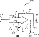
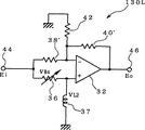
上述した同調増幅器の第1〜第4の実施形態において、2つの移相回路10Cおよび30C等を含む全域通過回路と帰還抵抗70からなる帰還ループのオープンループゲインの損失は、前段の移相回路10C等の入力インピーダンスに起因するものであるから、この入力インピーダンスに起因する損失の発生を抑えるために、前段の移相回路10C等のさらに前段にトランジスタによるホロワ回路を挿入し、帰還される信号をこのホロワ回路を介して前段の移相回路10C等に入力するようにしてもよい。
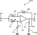
第17図は、同調増幅器の第5の実施形態の構成を示す回路図であり、第1図に示した同調増幅器1内部の前段の移相回路10Cのさらに前段にトランジスタによるホロワ回路50を挿入したものである。
このホロワ回路50は、ドレインが正電源Vddに、ソースが抵抗54を介して負電源Vssにそれぞれ接続されたFET52を含んで構成されている。これらFET52と抵抗54によりソースホロワ回路が形成されており、このソースホロワ回路の出力が前段の移相回路10Cに入力されている。なお、ソースホロワ回路の代わりにエミッタホロワ回路を用いるようにしてもよい。
このように、前段の移相回路10C等のさらに前段にトランジスタによるホロワ回路を縦続接続すれば、第1図等に示した同調増幅器1等と比較して、帰還抵抗70および入力抵抗74の抵抗値を高く設定することができる。特に、同調増幅器1等を半導体基板上に集積化するような場合には、帰還抵抗70等の抵抗値を小さくしようとすると素子の占有面積を大きくしなければならないため、ある程度抵抗値が大きい方が好ましく、ホロワ回路を接続する意義がある。
〔その他の実施形態〕
なお、本発明は上述した各種の実施形態に限定されるものではなく、この発明の要旨の範囲内で種々の変形実施が可能である。
例えば、上述した同調増幅器1等では、前段に移相回路10Cや110Cを、後段に30Cや130Cをそれぞれ配置したが、2つの移相回路全体で入出力信号間の位相シフト量が360゜となればよいことから、前後を入れ替えて前段に移相回路30Cや130Cを、後段に移相回路10Cや110Cをそれぞれ配置して同調増幅器を構成してもよい。
すなわち、本発明の同調増幅器は、第2図に示す移相回路10C、第9図に示す移相回路10L、第13図に示す移相回路110C、および第15図に示す移相回路110Lのうちいずれか一つと、第4図に示す移相回路30C、第11図に示す移相回路30L、第13図に示す移相回路130C、および第16図に示す移相回路130Lのうちいずれか一つとを任意の順序で縦続接続して構成することができる。
また、これら縦続接続された2つの移相回路のうち、一方の移相回路については、移相回路内の分圧回路を省略し、あるいは分圧比を1に設定してもよい。同様に、縦続接続された2つの移相回路のうち、一方の移相回路については、オペアンプの反転入力端子と接地端子間に接続された抵抗(例えば、第13図に示す抵抗22)を省略するか、その抵抗の抵抗値を十分に大きくしてもよい。また、縦続接続された2つの移相回路のうち、前段の移相回路のさらに前段にホロワ回路50を接続してもよい。
また、上述した同調増幅器1等に含まれる移相回路10C等には可変抵抗16や36が含まれている。この可変抵抗16や36はさらに具体的には接合型あるいはMOS型の電界効果トランジスタ(FET)のチャネル抵抗を利用して実現することができる。FETのソース・ドレイン間に形成されるチャネルを抵抗体として利用して可変抵抗16の代わりに使用すると、ゲート電圧を可変に制御してこのチャネル抵抗をある範囲で任意に変化させて各移相回路における位相シフト量を変えることができる。
また、可変抵抗16や36を1つのFET、すなわちpチャネルあるいはnチャネルのFETによって構成する代わりに、pチャネルのFETとnチャネルのFETとを並列接続して1つの可変抵抗を構成してもよい。2つのFETを組み合わせて可変抵抗を構成すれば、FETの非線形領域の改善を行うことができるため、同調信号の歪みを軽減できる。
また、上述した移相回路10C等は、キャパシタ14等と直列に接続された可変抵抗16等の抵抗値を変化させて位相シフト量を変化させることにより全体の同調周波数を変えるようにしたが、キャパシタ14等の静電容量を変化させることにより全体の同調周波数を変えるようにしてもよい。
例えば、2つの移相回路の中の少なくとも一方に含まれるキャパシタ14等を可変容量素子に置き換えてこの静電容量を可変することにより、各移相回路による移相シフト量を変化させて同調周波数を変えることができる。さらに具体的には、上述した可変容量素子をアノード・カソード間に印加する逆バイアス電圧が変更可能な可変容量ダイオードによって、あるいはゲート電圧によってゲート容量が変更可能なFETによって形成することができる。
なお、上述した可変容量素子に印加する逆バイアス電圧を可変するには、この可変容量素子と直列に直流電流阻止用のキャパシタを接続すればよい。
また、上述したように可変抵抗や可変容量素子を用いる場合の他、素子定数が異なる複数の抵抗、キャパシタあるいはインダクタを用意しておいて、スイッチを切り換えることにより、これら複数の素子の中から1つあるいは複数を選ぶようにしてもよい。この場合にはスイッチ切り換えにより接続する素子の個数および接続方法(直列接続、並列接続あるいはこれらの組み合わせ)によって、素子定数を不連続に切り換えることができる。
例えば、可変抵抗の代わりに抵抗値がR、2R、4R、…といった2のn乗の系列の複数の抵抗を用意しておいて、1つあるいは任意の複数を選択して直列接続することにより、等間隔の抵抗値の切り換えをより少ない素子で容易に実現することができる。同様に、キャパシタの代わりに静電容量がC、2C、4C、…といった2のn乗の系列の複数のキャパシタを用意しておいて、1つあるいは任意の複数を選択して並列接続することにより、等間隔の静電容量の切り換えをより少ない素子で容易に実現することができる。このため、同調周波数が複数ある回路、例えばAMラジオにこの実施形態の同調増幅器を適用して、複数の放送局から1局を選局して受信するような用途に適している。
また、上述した同調増幅器1等では、帰還インピーダンス素子として抵抗値が固定の帰還抵抗70を用い、入力インピーダンス素子として抵抗値が固定の入力抵抗74を用いるようにしたが、少なくとも一方の抵抗を可変抵抗により構成して、同調増幅器1等における同調帯域幅や最大減衰量を可変するようにしてもよい。
また、上述した各実施形態においては、オペアンプを用いて移相回路10C、30C等を構成することにより安定度の高い回路を構成することができるが、上述した各実施形態のような使い方をする場合にはオフセット電圧や電圧利得はそれほど高性能なものが要求されないため、所定の増幅度を有する差動入力増幅器を各移相回路内のオペアンプの代わりに使用するようにしてもよい。
第18図は、オペアンプの構成の中で各実施形態の移相回路の動作に必要な部分を抽出した回路図であり、全体が所定の増幅度を有する差動入力増幅器として動作する。同図に示す差動入力増幅器は、FETにより構成された差動入力段100と、この差動入力段100に定電流を与える定電流回路102と、定電流回路102に所定のバイアス電圧を与えるバイアス回路104と、差動入力段100に接続された出力アンプ106とによって構成されている。同図に示すように、実際のオペアンプに含まれている電圧利得を稼ぐための多段増幅回路を省略して、差動入力増幅器の構成を簡略化し、広帯域化を図ることができる。このように、回路の簡略化を行うことにより、動作周波数の上限を高くすることができるため、その分この差動入力増幅器を用いて構成した同調増幅器の同調周波数の上限を高くすることができる。
また、上述した各実施形態の同調増幅器は、後段の移相回路30C等の出力端46を同調増幅器の出力端子92に接続して同調信号を取り出したが、前段の移相回路10C等や第17図に示すホロワ回路50から同調信号を取り出すようにしてもよい。また、後段の移相回路30C等の前後から、あるいは前段の移相回路10C等の前後から互いに所定の位相差を有する2相出力を取り出すようにしてもよい。
また、第1図および第13図に示した同調増幅器1、1Aにおいては、後段の移相回路30Cのさらに後段に分圧回路60を接続したが、移相回路10Cと30Cの間、あるいはホロワ回路50の前後のいずれかに分圧回路60を挿入するようにしてもよい。この場合には、分圧回路60の出力を次段の回路に入力するとともに、分圧回路60による分圧前の信号を同調増幅器の出力として取り出せばよい。
産業上の利用可能性
以上の各実施形態に基づく説明から明らかなように、同調周波数を可変した場合に、その下限近傍から上限近傍までの広範囲にわたって振幅変動がなくほぼ一定の安定した同調出力を得ることができる。特に、同調周波数を可変した際の出力振幅の変動を抑えることにより、帰還抵抗と入力抵抗の抵抗比nを大きくして同調増幅器のQの値を大きくすることができる。
また、この発明の同調増幅器は、最大減衰量が入力インピーダンス素子と帰還インピーダンス素子の抵抗比nによって決まるとともに、同調周波数が各移相回路におけるCR回路やLR回路の時定数によって決まるため、最大減衰量や同調周波数および同調周波数における利得を互いに干渉しあうことなく設定することができる。
また、この発明の同調増幅器は、帰還ループ内に分圧回路を挿入することにより、同調動作と増幅動作を1つの回路で同時に行うことができる。これにより、この同調増幅器を含む装置全体の簡略化等が実現できる。
また、同調増幅器内の2つの移相回路をCR回路を含んで構成した場合には、同調増幅器全体を容易に集積化することができる。同様に、2つの移相回路をLR回路を含んで構成した場合には、集積化によって小さなインダクタを形成することにより容易に同調周波数の高周波化が可能となる。一方の移相回路をCR回路を含んで、他方の移相回路をLR回路を含んで構成した場合には、温度等による特性の変動を防止して特性の安定化が可能となる。Technical field
The present invention relates to a tuning amplifier that can be easily integrated, and more particularly to a tuning amplifier that can arbitrarily adjust a tuning frequency and a maximum attenuation amount without interfering with each other.
Background art
Conventionally, various tuning amplifiers using active elements and reactance elements have been proposed and put into practical use.
For example, in a conventional tuning amplifier using LC resonance, Q and gain depending on the LC circuit change when the tuning frequency is adjusted, the tuning frequency changes when the maximum attenuation is adjusted, and at the tuning frequency when the maximum attenuation is adjusted. It has the feature that the gain changes. Therefore, in the conventional tuning amplifier, it is extremely difficult to adjust the tuning frequency, the gain at the tuning frequency, and the maximum attenuation amounts C1 and C2 without interfering with each other. In addition, it has been difficult to form a tuning amplifier that can adjust the tuning frequency and the maximum attenuation amount by an integrated circuit.
The present invention was created in view of the above points, and its purpose is suitable for integration, and it is possible to adjust the tuning frequency, the gain at the tuning frequency, and the maximum attenuation without interfering with each other. In particular, it is an object of the present invention to provide a tuning amplifier that can suppress a change in output amplitude when the tuning frequency is varied.
Disclosure of the invention
The present invention has been conceived to solve such a problem, and the tuning frequency, the gain at the tuning frequency, and the maximum attenuation can be adjusted without interfering with each other, particularly when the tuning frequency is varied. An object of the present invention is to provide a tuning amplifier capable of suppressing a change in output amplitude.
The tuning amplifier of the present invention includes two all-pass type phase shift circuits including a differential amplifier whose output is fed back to the input side,
A voltage dividing circuit inserted into a part of a feedback loop formed by cascading each of the two phase shift circuits,
The signal added by the adder circuit is input to the previous phase shift circuit of the two cascaded phase shift circuits, and the signal output from the subsequent phase shift circuit is used as the feedback signal as the feedback signal. An AC signal input to the circuit and input to the voltage dividing circuit is output as the tuning signal.
The tuned amplifier of the present invention includes an input impedance element in which an input signal is input to one end and a feedback impedance element in which a feedback signal is input to one end, and the input signal and the feedback signal are An adding circuit for adding;
A differential amplifier in which one end of a first resistor is connected to an inverting input terminal and an AC signal is input through the first resistor, and a first voltage dividing circuit connected to the output terminal of the differential amplifier And a second resistor connected between the output terminal of the first voltage dividing circuit and the inverting input terminal of the differential amplifier, a reactance element such as a capacitor or an inductor, and a third resistor. Two phase shift circuits including a series circuit connected to the other end of the first resistor, and connecting a connection portion of the third resistor and the reactance element to a non-inverting input terminal of the differential amplifier;
Each of the two phase shift circuits is connected in cascade, and the signal added by the adder circuit is input to the previous phase shift circuit among the two phase shift circuits connected in cascade. The signal output from the phase shift circuit is input to the one end of the feedback impedance element as the feedback signal, and the output of either of these two phase shift circuits is output as the tuning signal.
The tuned amplifier of the present invention includes an input impedance element in which an input signal is input to one end and a feedback impedance element in which a feedback signal is input to one end, and the input signal and the feedback signal are An adding circuit for adding;
A differential amplifier to which one end of the first resistor of the inverting input terminal is connected and an AC signal is input via the first resistor, and is connected between the inverting input terminal and the output terminal of the differential amplifier. A second resistor, a third resistor having one end connected to the inverting input terminal of the differential amplifier and the other end grounded, a reactance element such as a capacitor or an inductor, and a fourth resistor. Two phase shift circuits including a series circuit connected to the other end of the first resistor, and a connection portion of the fourth resistor and the reactance element connected to a non-inverting input terminal of the differential amplifier;
Each of the two phase shift circuits is connected in cascade, and the signal added by the adder circuit is input to the previous phase shift circuit among the two phase shift circuits connected in cascade. The signal output from the phase shift circuit is input to the one end of the feedback impedance element as the feedback signal, and the output of either of these two phase shift circuits is output as the tuning signal.
The tuned amplifier of the present invention includes an input impedance element in which an input signal is input to one end and a feedback impedance element in which a feedback signal is input to one end, and the input signal and the feedback signal are An adding circuit for adding;
A differential amplifier in which one end of a first resistor is connected to an inverting input terminal and an AC signal is input through the first resistor, and a first voltage dividing circuit connected to the output terminal of the differential amplifier And a second resistor connected between the output terminal of the first voltage dividing circuit and the inverting input terminal of the differential amplifier, a reactance element such as a capacitor or an inductor, and a third resistor. A first phase shift circuit including a series circuit connected to the other end of the first resistor, and a connection portion of the third resistor and the reactance element connected to a non-inverting input terminal of the differential amplifier;
A differential amplifier in which one end of a fourth resistor is connected to the inverting input terminal and an AC signal is input through the fourth resistor, and is connected between the inverting input terminal and the output terminal of the differential amplifier. A fifth resistor, a sixth resistor having one end connected to the inverting input terminal of the differential amplifier and the other end grounded, a reactance element such as a capacitor or an inductor, and a seventh resistor. A series circuit connected to the other end of the four resistors, and a second phase shift circuit in which a connection portion of the seventh resistor and the reactance element is connected to a non-inverting input terminal of the differential amplifier;
The first and second phase shift circuits are connected in cascade, and the signal added by the adder circuit is input to the previous phase shift circuit of the two phase shift circuits connected in cascade. The signal output from the subsequent phase shift circuit is input to the one end of the feedback impedance element as the feedback signal, and the output of one of the first and second phase shift circuits is output as the tuning signal.
[Brief description of the drawings]
FIG. 1 is a circuit diagram showing a configuration of a tuning amplifier according to a first embodiment to which the present invention is applied;
FIG. 2 is a diagram showing an extracted configuration of the previous phase shift circuit shown in FIG.
FIG. 3 is a vector diagram showing the relationship between the input / output voltage of the previous phase shift circuit and the voltage appearing on the capacitor,
FIG. 4 is a diagram showing the configuration of the subsequent phase shift circuit shown in FIG.
FIG. 5 is a vector diagram showing the relationship between the input / output voltage of the subsequent phase shift circuit and the voltage appearing on the capacitor,
FIG. 6 is a system diagram in which two phase shift circuits and voltage divider circuits having the above-described configuration are replaced with a circuit having a transfer function K1,
FIG. 7 is a system diagram in which the system shown in FIG. 6 is replaced by the mirror theorem.
FIG. 8 is a diagram showing the tuning characteristics of the tuning amplifier shown in FIG.
FIG. 9 is a circuit diagram showing a configuration of a phase shift circuit including an LR circuit,
FIG. 10 is a vector diagram showing the relationship between the input / output voltage of the phase shift circuit shown in FIG. 9 and the voltage appearing in the inductor, etc.
FIG. 11 is a circuit diagram showing the configuration of another phase shift circuit including the LR circuit,
FIG. 12 is a vector diagram showing the relationship between the input / output voltage of the phase shift circuit shown in FIG. 11 and the voltage appearing in the inductor,
FIG. 13 is a circuit diagram showing a third embodiment of the tuning amplifier;
FIG. 14 is a generalized diagram of the phase shift circuit shown in FIG.
FIG. 15 is a circuit diagram showing the configuration of a phase shift circuit that can be replaced with the phase shift circuit in the previous stage of the tuning amplifier shown in FIG.
FIG. 16 is a circuit diagram showing a configuration of a phase shift circuit that can be replaced with a phase shift circuit in the subsequent stage of the tuning amplifier shown in FIG.
FIG. 17 is a circuit diagram showing a configuration of a fifth embodiment of a tuning amplifier;
FIG. 18 is a circuit diagram in which a portion necessary for the operation of the phase shift circuit of the present invention is pushed out in the configuration of the operational amplifier.
BEST MODE FOR CARRYING OUT THE INVENTION
[First Embodiment of Tuning Amplifier]
FIG. 1 is a circuit diagram showing a configuration of a tuning amplifier according to a first embodiment to which the present invention is applied.
The
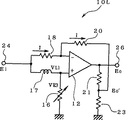
FIG. 2 shows an extracted configuration of the preceding
In the
When a predetermined AC signal is input to the
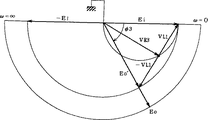
FIG. 3 is a vector diagram showing the relationship between the input / output voltage of the preceding
As described above, when the voltage VC1 applied to the non-inverting input terminal of the
Since the
Similarly, FIG. 4 shows an extracted configuration of the subsequent
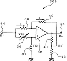
In the
When a predetermined AC signal is input to the
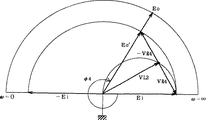
FIG. 5 is a vector diagram showing the relationship between the input / output voltage of the subsequent
As described above, considering the voltage VR2 applied to the non-inverting input terminal of the
Since the
In this way, the phase is shifted by a predetermined amount in each of the two
Further, the output of the subsequent
As described above, the total phase shift amount at a predetermined frequency is 360 ° by the two
Further, since the output of the
FIG. 6 is a system diagram in which the two
FIG. 7 is a system diagram in which the system shown in FIG. 6 is converted by Miller's theorem, and the transfer function A of the entire system after conversion is
A = Vo / Vi = K1 / {n (1-K1) +1} (1)
Can be expressed as
The transfer function K2 of the preceding
K2 = a1(1-T1s) / (1 + T1s) (2)
It becomes. Where s = jω and a1Is the gain of the
Further, the transfer function K3 of the subsequent
K3 = -a2(1-T2s) / (1 + T2s) (3)
It becomes. Where a2Is the gain of the
The signal amplitude is 1 / a through the voltage divider circuit 60.1a2When the two
K1 =-{1+ (Ts)2-2Ts} / {1+ (Ts)2+ 2Ts} (4)
It becomes. In the above equation (4), in order to simplify the calculation, the time constant T of each phase shift circuit is set.1, T2Both are T. Substituting this equation (4) into the above equation (1),
A =-{1+ (Ts)2−2Ts}
/ [(2n + 1) {1+ (Ts)2} + 2Ts]
=-{1 / (2n + 1)} [{1+ (Ts)2−2Ts}
/ {1+ (Ts)2+ 2Ts / (2n + 1)}] (5)
It becomes.
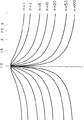
According to the equation (5), it can be seen that when ω = 0 (DC region), A = −1 / (2n + 1), and the maximum attenuation is given. It can also be seen that even when ω = ∞, A = −1 / (2n + 1), giving the maximum attenuation. Furthermore, the tuning point of ω = 1 / T (if the time constant of each phase shift circuit is different,
![]()
Incidentally, in FIG. 6 described above, when the all-pass circuit indicated by the transfer function K1 has an input impedance, a voltage dividing circuit is formed by the
For example, the voltage dividing circuit by the
By adding a voltage dividing circuit consisting of a
As described above, by changing the resistance values of the
![]()
Further, when φ1 and φ2 shown in FIG. 3 and FIG. 5 are obtained from the equation (2) or (3),
φ1 = tan {2ωT1/ (1-ω2T1 2)} (6)
φ2 = tan {2ωT2/ (1-ω2T2 2)} (7)
It becomes. In the equations (6) and (7), φ1 and φ2 are obtained by setting the clockwise direction (phase delay direction) as the positive direction with reference to the input voltage Ei shown in FIGS.
For example T1= T2In the case of (= T), when ω = 1 / T, the total phase shift amount by the two
As described above, the
In the first embodiment described above, the resistance values of the
In the
In particular, by suppressing the amplitude fluctuation of the tuning output, the resistance ratio n described above can be increased and the Q value of the
Further, the signal attenuated through the
Further, since the maximum attenuation is determined by the resistance ratio n of the
Furthermore, the
In addition, by continuously changing the resistance value of at least one of the
When the
As described above, when the voltage dividing circuit is omitted for one of the two cascaded phase shift circuits and the gain is set to 1, the gain of the other
When the amplification operation is unnecessary, the
[Second Embodiment]
In the
FIG. 9 is a circuit diagram showing the configuration of the phase shift circuit including the LR circuit, and shows a configuration that can be replaced with the
Therefore, the relationship between the input / output voltages and the like of the phase shift circuit 10L described above is such that the voltage VC1 shown in FIG. 3 is changed to the voltage VR3 across the
The transfer function of the phase shift circuit 10L shown in FIG. 9 is the time constant of the LR circuit composed of the
Thus, the phase shift circuit 10L shown in FIG. 9 is basically equivalent to the
FIG. 11 is a circuit diagram showing another configuration of the phase shift circuit including the LR circuit, and shows a configuration that can replace the
Therefore, the relationship between the input / output voltages and the like of the
By the way, the transfer function of the
Thus, one or both of the two
In addition, when only one of the two
When at least one of the
[Third Embodiment]
FIG. 13 is a circuit diagram showing a third embodiment of the tuning amplifier. The tuning amplifier 1A shown in FIG. 1 includes two
In the
The same applies to the subsequent
In the tuning amplifier 1A shown in FIG. 13, a voltage dividing circuit may be further connected to the subsequent stage of the subsequent
By the way, when the gain of each phase shift circuit is set to a value larger than 1, gain fluctuations occur according to the frequency of the input signal. For example, in the case of the phase-
Such amplitude fluctuation can be suppressed by connecting the
Next, what value should be set for the resistance value of the resistor 22 (or resistor 42) is examined. FIG. 14 is a diagram in which the above-described
Between the input voltage Ei and the voltage V,
r (I a + I b) + V = Ei (8)
There is a relationship. Moreover, when the voltage V is expressed using various constants shown in FIG.
V = I b R (9)
V = Eo + mr · I a (10)
V = {z2 / (z1 + z2)} Ei = kEi (11)
It becomes. In the equation (11), the voltage division ratio by two elements having impedances z1 and z2 is k.
If I a is obtained from the equation (10) and I b is obtained from the equation (9), and these are substituted into the equation (8). Further, the equation (11) is substituted into the substituted result, and V is deleted.
Eo = (Rk + Rmk + mrk−Rm) Ei / R (12)
It becomes.
By the way, the case where the phase shift circuit shown in FIG. 14 operates as an inverting amplifier is a case where the impedance z2 is 0Ω and k = 0.
Eo = −mEi (13)
It becomes. Also, the case where the phase shift circuit shown in FIG. 14 operates as a follower circuit is a case where the impedance z1 is 0Ω and k = 1.
Eo = (R + mr) Ei / R (14)
It becomes. When there is no gain fluctuation when the phase-
m = (R + mr) / R (15)
It becomes. Solving for R,
R = mr / (m−1) (16)
It becomes. Therefore, the tuning frequency is changed from a low frequency to a high frequency by setting the resistance value R of the
[Fourth Embodiment]
In the tuning amplifier 1A shown in FIG. 13, the example in which the CR circuit is included in the
FIG. 15 is a circuit diagram showing a configuration of a phase shift circuit including an LR circuit, and shows a configuration that can replace the
FIG. 16 is a circuit diagram showing another configuration of the phase shift circuit including the LR circuit, and shows a configuration that can replace the
Each of the
By the way, the tuning amplifier 1A shown in FIG. 13 prevents the amplitude fluctuation when the tuning frequency is varied by connecting the
[Fifth Embodiment]
In the first to fourth embodiments of the tuning amplifier described above, the loss of the open loop gain of the feedback loop including the all-pass circuit including the two
FIG. 17 is a circuit diagram showing the configuration of the fifth embodiment of the tuning amplifier, and a
The
In this way, if a transistor follower circuit is cascade-connected to the preceding stage such as the preceding
[Other Embodiments]
The present invention is not limited to the various embodiments described above, and various modifications can be made within the scope of the present invention.
For example, in the
That is, the tuning amplifier of the present invention includes a
Of the two phase shift circuits connected in cascade, one of the phase shift circuits may omit the voltage dividing circuit in the phase shifting circuit or set the voltage dividing ratio to 1. Similarly, of two phase shift circuits connected in cascade, one of the phase shift circuits omits the resistor (for example, the
The
Further, instead of configuring the
The
For example, by changing the capacitance by replacing the
In order to vary the reverse bias voltage applied to the above-described variable capacitance element, a DC current blocking capacitor may be connected in series with the variable capacitance element.
In addition to the case of using a variable resistor or variable capacitance element as described above, a plurality of resistors, capacitors, or inductors having different element constants are prepared, and one of the plurality of elements is switched by switching the switch. One or more may be selected. In this case, the element constants can be switched discontinuously depending on the number of elements to be connected by switching and the connection method (series connection, parallel connection, or a combination thereof).
For example, instead of a variable resistor, a plurality of resistors in the n-th power series such as R, 2R, 4R,... Are prepared, and one or an arbitrary plurality are selected and connected in series. The switching of resistance values at equal intervals can be easily realized with fewer elements. Similarly, instead of capacitors, prepare a plurality of 2 n series capacitors with capacitances C, 2C, 4C,..., Select one or any plurality and connect them in parallel Thus, switching of the capacitance at equal intervals can be easily realized with fewer elements. For this reason, the tuning amplifier of this embodiment is applied to a circuit having a plurality of tuning frequencies, for example, an AM radio, and is suitable for an application in which one station is selected and received from a plurality of broadcasting stations.
In the
In each of the above-described embodiments, a circuit with high stability can be configured by configuring the
FIG. 18 is a circuit diagram in which a portion necessary for the operation of the phase shift circuit of each embodiment is extracted from the configuration of the operational amplifier, and the whole operates as a differential input amplifier having a predetermined amplification degree. The differential input amplifier shown in FIG. 1 includes a
In the tuning amplifiers of the above-described embodiments, the
Further, in the
Industrial applicability
As is clear from the description based on each of the above embodiments, when the tuning frequency is varied, an almost constant and stable tuning output can be obtained with no amplitude fluctuation over a wide range from the vicinity of the lower limit to the vicinity of the upper limit. In particular, by suppressing fluctuations in the output amplitude when the tuning frequency is varied, the resistance ratio n between the feedback resistor and the input resistor can be increased, and the Q value of the tuning amplifier can be increased.
In the tuning amplifier of the present invention, the maximum attenuation is determined by the resistance ratio n between the input impedance element and the feedback impedance element, and the tuning frequency is determined by the time constant of the CR circuit and the LR circuit in each phase shift circuit. The quantity, the tuning frequency and the gain at the tuning frequency can be set without interfering with each other.
In addition, the tuning amplifier of the present invention can perform the tuning operation and the amplification operation simultaneously with one circuit by inserting a voltage dividing circuit in the feedback loop. Thereby, simplification of the entire apparatus including the tuning amplifier can be realized.
Further, when the two phase shift circuits in the tuning amplifier include the CR circuit, the entire tuning amplifier can be easily integrated. Similarly, when the two phase shift circuits are configured to include the LR circuit, the tuning frequency can be easily increased by forming a small inductor by integration. When one phase shift circuit includes a CR circuit and the other phase shift circuit includes an LR circuit, the characteristics can be stabilized by preventing variation in characteristics due to temperature or the like.
Claims (37)
出力が入力側に帰還された差動増幅器を含む全域通過型の2つの移相回路と、
前記2つの移相回路のそれぞれを縦続接続して形成される帰還ループの一部に挿入される分圧回路とを備え、
前記縦続接続された2つの移相回路のうち前段の移相回路に対して前記加算回路によって加算された信号を入力するとともに、後段の移相回路から出力された信号を前記帰還信号として前記加算回路に入力し、前記分圧回路に入力される交流信号を前記同調信号として出力することを特徴とする同調増幅器。An adding circuit for adding the input signal and the feedback signal;
Two phase shift circuits including a differential amplifier whose output is fed back to the input side;
A voltage dividing circuit inserted into a part of a feedback loop formed by cascading each of the two phase shift circuits,
The signal added by the adder circuit is input to the previous phase shift circuit of the two cascaded phase shift circuits, and the signal output from the subsequent phase shift circuit is used as the feedback signal as the feedback signal. A tuning amplifier that inputs to a circuit and outputs an AC signal input to the voltage dividing circuit as the tuning signal.
反転入力端子に第1の抵抗の一方端が接続され前記第1の抵抗を介して交流信号が入力される差動増幅器と、前記差動増幅器の出力端子に接続された第1の分圧回路と、前記第1の分圧回路の出力端と前記差動増幅器の反転入力端子との間に接続された第2の抵抗と、キャパシタあるいはインダクタによるリアクタンス素子と第3の抵抗とで構成され前記第1の抵抗の他方端に接続された直列回路とを含み、前記第3の抵抗および前記リアクタンス素子の接続部を前記差動増幅器の非反転入力端子に接続した2つの移相回路と、
を備え、前記2つの移相回路のそれぞれを縦続接続し、これら縦続接続された2つの移相回路のうち前段の移相回路に対して前記加算回路によって加算された信号を入力するとともに、後段の移相回路から出力された信号を前記帰還信号として前記帰還インピーダンス素子の一方端に入力し、これら2つの移相回路のいずれかの出力を同調信号として出力することを特徴とする同調増幅器。An addition circuit that includes an input impedance element that is input to one end of the input signal and a feedback impedance element that is input to the other end of the feedback signal, and adds the input signal and the feedback signal;
A differential amplifier in which one end of a first resistor is connected to an inverting input terminal and an AC signal is input through the first resistor, and a first voltage dividing circuit connected to the output terminal of the differential amplifier And a second resistor connected between the output terminal of the first voltage dividing circuit and the inverting input terminal of the differential amplifier, a reactance element such as a capacitor or an inductor, and a third resistor. Two phase shift circuits including a series circuit connected to the other end of the first resistor, and connecting a connection portion of the third resistor and the reactance element to a non-inverting input terminal of the differential amplifier;
Each of the two phase shift circuits is connected in cascade, and the signal added by the adder circuit is input to the previous phase shift circuit among the two phase shift circuits connected in cascade. A tuning amplifier characterized in that the signal output from the phase shift circuit is input to the one end of the feedback impedance element as the feedback signal, and the output of either of the two phase shift circuits is output as a tuning signal.
反転入力端子に第1の抵抗の一方端が接続され前記第1の抵抗を介して交流信号が入力される差動増幅器と、前記差動増幅器の反転入力端子と出力端子との間に接続された第2の抵抗と、一方端が前記差動増幅器の反転入力端子に接続され他方端が接地された第3の抵抗と、キャパシタあるいはインダクタによるリアクタンス素子と第4の抵抗とで構成され前記第1の抵抗の他方端に接続された直列回路とを含み、前記第4の抵抗および前記リアクタンス素子の接続部を前記差動増幅器の非反転入力端子に接続した2つの移相回路と、
を備え、前記2つの移相回路のそれぞれを縦続接続し、これら縦続接続された2つの移相回路のうち前段の移相回路に対して前記加算回路によって加算された信号を入力するとともに、後段の移相回路から出力された信号を前記帰還信号として前記帰還インピーダンス素子の一方端に入力し、これら2つの移相回路のいずれかの出力を同調信号として出力することを特徴とする同調増幅器。An addition circuit that includes an input impedance element that is input to one end of the input signal and a feedback impedance element that is input to the other end of the feedback signal, and adds the input signal and the feedback signal;
A differential amplifier in which one end of the first resistor is connected to the inverting input terminal and an AC signal is input through the first resistor, and is connected between the inverting input terminal and the output terminal of the differential amplifier. A second resistor, a third resistor having one end connected to the inverting input terminal of the differential amplifier and the other end grounded, a reactance element such as a capacitor or an inductor, and a fourth resistor. Two phase shift circuits including a series circuit connected to the other end of the first resistor, and a connection portion of the fourth resistor and the reactance element connected to a non-inverting input terminal of the differential amplifier;
Each of the two phase shift circuits is connected in cascade, and the signal added by the adder circuit is input to the previous phase shift circuit among the two phase shift circuits connected in cascade. A tuning amplifier characterized in that the signal output from the phase shift circuit is input to the one end of the feedback impedance element as the feedback signal, and the output of either of the two phase shift circuits is output as a tuning signal.
反転入力端子に第1の抵抗の一方端が接続され前記第1の抵抗を介して交流信号が入力される差動増幅器と、前記差動増幅器の出力端子に接続された第1の分圧回路と、前記第1の分圧回路の出力端と前記差動増幅器の反転入力端子との間に接続された第2の抵抗と、キャパシタあるいはインダクタによるリアクタンス素子と第3の抵抗とで構成され前記第1の抵抗の他方端に接続された直列回路とを含み、前記第3の抵抗および前記リアクタンス素子の接続部を前記差動増幅器の非反転入力端子に接続した第1の移相回路と、
反転入力端子に第4の抵抗の一方端が接続され前記第4の抵抗を介して交流信号が入力される差動増幅器と、前記差動増幅器の反転入力端子と出力端子との間に接続された第5の抵抗と、一方端が前記差動増幅器の反転入力端子に接続され他方端が接地された第6の抵抗と、キャパシタあるいはインダクタによるリアクタンス素子と第7の抵抗とで構成され前記第4の抵抗の他方端に接続された直列回路とを含み、前記第7の抵抗および前記リアクタンス素子の接続部を前記差動増幅器の非反転入力端子に接続した第2の移相回路と、
を備え、前記第1および第2の移相回路を縦続接続し、これら縦続接続された2つの移相回路のうち前段の移相回路に対して前記加算回路によって加算された信号を入力するとともに、後段の移相回路から出力された信号を前記帰還信号として前記帰還インピーダンス素子の一方端に入力し、前記第1および第2の移相回路のいずれかの出力を前記同調信号として出力することを特徴とする同調増幅器。An addition circuit that includes an input impedance element that is input to one end of the input signal and a feedback impedance element that is input to the other end of the feedback signal, and adds the input signal and the feedback signal;
A differential amplifier in which one end of a first resistor is connected to an inverting input terminal and an AC signal is input through the first resistor, and a first voltage dividing circuit connected to the output terminal of the differential amplifier And a second resistor connected between the output terminal of the first voltage dividing circuit and the inverting input terminal of the differential amplifier, a reactance element such as a capacitor or an inductor, and a third resistor. A first phase shift circuit including a series circuit connected to the other end of the first resistor, and a connection portion of the third resistor and the reactance element connected to a non-inverting input terminal of the differential amplifier;
A differential amplifier in which one end of a fourth resistor is connected to the inverting input terminal and an AC signal is input through the fourth resistor, and is connected between the inverting input terminal and the output terminal of the differential amplifier. A fifth resistor, a sixth resistor having one end connected to the inverting input terminal of the differential amplifier and the other end grounded, a reactance element such as a capacitor or an inductor, and a seventh resistor. A series circuit connected to the other end of the four resistors, and a second phase shift circuit in which a connection portion of the seventh resistor and the reactance element is connected to a non-inverting input terminal of the differential amplifier;
The first and second phase shift circuits are connected in cascade, and the signal added by the adder circuit is input to the previous phase shift circuit of the two phase shift circuits connected in cascade. The signal output from the subsequent phase shift circuit is input to the one end of the feedback impedance element as the feedback signal, and the output of one of the first and second phase shift circuits is output as the tuning signal. A tuned amplifier.
Applications Claiming Priority (3)
| Application Number | Priority Date | Filing Date | Title |
|---|---|---|---|
| JP31366995 | 1995-11-07 | ||
| JP31367095 | 1995-11-07 | ||
| PCT/JP1996/000530 WO1997017754A1 (en) | 1995-11-07 | 1996-03-06 | Tuning amplifier |
Publications (1)
| Publication Number | Publication Date |
|---|---|
| JP3628334B2 true JP3628334B2 (en) | 2005-03-09 |
Family
ID=26567661
Family Applications (1)
| Application Number | Title | Priority Date | Filing Date |
|---|---|---|---|
| JP51804497A Expired - Fee Related JP3628334B2 (en) | 1995-11-07 | 1996-03-06 | Tuning amplifier |
Country Status (10)
| Country | Link |
|---|---|
| US (1) | US6034566A (en) |
| EP (1) | EP0860942B1 (en) |
| JP (1) | JP3628334B2 (en) |
| KR (1) | KR19990028989A (en) |
| CN (1) | CN1084962C (en) |
| AU (1) | AU4889196A (en) |
| DE (1) | DE69636411D1 (en) |
| HK (1) | HK1016760A1 (en) |
| TW (1) | TW291625B (en) |
| WO (1) | WO1997017754A1 (en) |
Families Citing this family (31)
| Publication number | Priority date | Publication date | Assignee | Title |
|---|---|---|---|---|
| US6061551A (en) | 1998-10-21 | 2000-05-09 | Parkervision, Inc. | Method and system for down-converting electromagnetic signals |
| US7515896B1 (en) | 1998-10-21 | 2009-04-07 | Parkervision, Inc. | Method and system for down-converting an electromagnetic signal, and transforms for same, and aperture relationships |
| US7236754B2 (en) | 1999-08-23 | 2007-06-26 | Parkervision, Inc. | Method and system for frequency up-conversion |
| US7039372B1 (en) | 1998-10-21 | 2006-05-02 | Parkervision, Inc. | Method and system for frequency up-conversion with modulation embodiments |
| US6370371B1 (en) | 1998-10-21 | 2002-04-09 | Parkervision, Inc. | Applications of universal frequency translation |
| US6813485B2 (en) * | 1998-10-21 | 2004-11-02 | Parkervision, Inc. | Method and system for down-converting and up-converting an electromagnetic signal, and transforms for same |
| US6879817B1 (en) * | 1999-04-16 | 2005-04-12 | Parkervision, Inc. | DC offset, re-radiation, and I/Q solutions using universal frequency translation technology |
| US6853690B1 (en) | 1999-04-16 | 2005-02-08 | Parkervision, Inc. | Method, system and apparatus for balanced frequency up-conversion of a baseband signal and 4-phase receiver and transceiver embodiments |
| US7110435B1 (en) * | 1999-03-15 | 2006-09-19 | Parkervision, Inc. | Spread spectrum applications of universal frequency translation |
| US7693230B2 (en) | 1999-04-16 | 2010-04-06 | Parkervision, Inc. | Apparatus and method of differential IQ frequency up-conversion |
| US7065162B1 (en) | 1999-04-16 | 2006-06-20 | Parkervision, Inc. | Method and system for down-converting an electromagnetic signal, and transforms for same |
| US7110444B1 (en) | 1999-08-04 | 2006-09-19 | Parkervision, Inc. | Wireless local area network (WLAN) using universal frequency translation technology including multi-phase embodiments and circuit implementations |
| US8295406B1 (en) | 1999-08-04 | 2012-10-23 | Parkervision, Inc. | Universal platform module for a plurality of communication protocols |
| US7010286B2 (en) | 2000-04-14 | 2006-03-07 | Parkervision, Inc. | Apparatus, system, and method for down-converting and up-converting electromagnetic signals |
| US7454453B2 (en) | 2000-11-14 | 2008-11-18 | Parkervision, Inc. | Methods, systems, and computer program products for parallel correlation and applications thereof |
| US7010559B2 (en) * | 2000-11-14 | 2006-03-07 | Parkervision, Inc. | Method and apparatus for a parallel correlator and applications thereof |
| US6492876B1 (en) * | 2001-10-25 | 2002-12-10 | National Semiconductor Corporation | Low power analog equalizer with variable op-amp gain |
| US7072427B2 (en) | 2001-11-09 | 2006-07-04 | Parkervision, Inc. | Method and apparatus for reducing DC offsets in a communication system |
| US7379883B2 (en) | 2002-07-18 | 2008-05-27 | Parkervision, Inc. | Networking methods and systems |
| US7460584B2 (en) | 2002-07-18 | 2008-12-02 | Parkervision, Inc. | Networking methods and systems |
| US7116163B2 (en) * | 2004-08-02 | 2006-10-03 | Broadcom Corporation | Buffer circuit |
| DE102006045279A1 (en) * | 2006-01-31 | 2007-08-09 | Micro-Epsilon Messtechnik Gmbh & Co. Kg | Circuit for setting an impedance |
| CN101420209B (en) * | 2008-11-21 | 2011-08-31 | 北京时代民芯科技有限公司 | High speed large dynamic range digital automatic gain control circuit |
| KR101666877B1 (en) | 2011-10-12 | 2016-10-18 | 삼성에스디아이 주식회사 | Rechargeable lithium battery |
| US9595931B2 (en) * | 2014-09-12 | 2017-03-14 | Ess Technology, Inc. | Two differential amplifier configuration |
| CN105450198A (en) * | 2015-12-31 | 2016-03-30 | 陕西烽火电子股份有限公司 | Dielectric resonator type electrically tunable filter |
| CN108111010A (en) * | 2017-03-20 | 2018-06-01 | 中惠创智无线供电技术有限公司 | A kind of power factor compensation system and power supply |
| US10986712B2 (en) * | 2017-09-30 | 2021-04-20 | Signify Holding B.V. | Controllable driver and drive method to connect an electronic ballast to an LED light source based on the model, type, or identity of the ballast |
| CN107967907B (en) * | 2018-01-18 | 2021-03-09 | 京东方科技集团股份有限公司 | Inverter circuit, driving method, array substrate, detection method and display device |
| US11552644B2 (en) * | 2020-01-19 | 2023-01-10 | Ixi Technology Holdings, Inc. | Fast frequency hopping of modulated signals |
| US20230179210A1 (en) * | 2021-12-08 | 2023-06-08 | SiliconIntervention Inc. | Analog Signal Time Gain Amplifier |
Family Cites Families (13)
| Publication number | Priority date | Publication date | Assignee | Title |
|---|---|---|---|---|
| US3434070A (en) * | 1966-01-14 | 1969-03-18 | Sylvania Electric Prod | Shunt feed for increasing amplifier output power |
| US4023113A (en) * | 1974-03-04 | 1977-05-10 | Hammond Corporation | Voltage controlled filter |
| US3972006A (en) * | 1974-09-20 | 1976-07-27 | Beckman Instruments, Inc. | Bandpass filter |
| DE2608431C3 (en) * | 1976-03-01 | 1978-08-17 | Siemens Ag, 1000 Berlin Und 8000 Muenchen | Coilless filter circuit formed from two all-pass elements of the first order |
| JPS5840935A (en) * | 1981-09-03 | 1983-03-10 | Fujitsu Ten Ltd | High frequency tuning circuit |
| JPH02130008A (en) * | 1988-11-09 | 1990-05-18 | Toshiba Corp | High frequency power amplification circuit |
| US4994761A (en) * | 1989-11-06 | 1991-02-19 | Motorola Inc. | VHF power amplifier |
| US5235223A (en) * | 1991-08-29 | 1993-08-10 | Harman International Industries, Inc. | Constant Q peaking filter utilizing synthetic inductor and simulated capacitor |
| JP2712923B2 (en) * | 1991-09-10 | 1998-02-16 | 富士通株式会社 | SAT phase shift circuit |
| US5329249A (en) * | 1993-10-13 | 1994-07-12 | Pacific Monolithics, Inc. | High efficiency RF power amplifier |
| KR100367070B1 (en) * | 1994-05-10 | 2003-03-15 | 타케시 이케다 | Tuning Amplifier |
| WO1995034953A1 (en) * | 1994-06-13 | 1995-12-21 | Takeshi Ikeda | Tuned amplifier |
| WO1996004712A1 (en) * | 1994-08-05 | 1996-02-15 | Takeshi Ikeda | Tuning amplifier |
-
1996
- 1996-03-06 JP JP51804497A patent/JP3628334B2/en not_active Expired - Fee Related
- 1996-03-06 KR KR1019980700291A patent/KR19990028989A/en not_active Application Discontinuation
- 1996-03-06 CN CN96196164A patent/CN1084962C/en not_active Expired - Fee Related
- 1996-03-06 DE DE69636411T patent/DE69636411D1/en not_active Expired - Lifetime
- 1996-03-06 AU AU48891/96A patent/AU4889196A/en not_active Abandoned
- 1996-03-06 WO PCT/JP1996/000530 patent/WO1997017754A1/en active IP Right Grant
- 1996-03-06 US US09/051,932 patent/US6034566A/en not_active Expired - Fee Related
- 1996-03-06 EP EP96905001A patent/EP0860942B1/en not_active Expired - Lifetime
- 1996-04-18 TW TW085104626A patent/TW291625B/en active
-
1998
- 1998-11-12 HK HK98111943A patent/HK1016760A1/en not_active IP Right Cessation
Also Published As
| Publication number | Publication date |
|---|---|
| TW291625B (en) | 1996-11-21 |
| WO1997017754A1 (en) | 1997-05-15 |
| KR19990028989A (en) | 1999-04-15 |
| CN1192829A (en) | 1998-09-09 |
| CN1084962C (en) | 2002-05-15 |
| HK1016760A1 (en) | 1999-11-05 |
| US6034566A (en) | 2000-03-07 |
| AU4889196A (en) | 1997-05-29 |
| DE69636411D1 (en) | 2006-09-14 |
| EP0860942A1 (en) | 1998-08-26 |
| EP0860942A4 (en) | 2004-03-10 |
| EP0860942B1 (en) | 2006-08-02 |
Similar Documents
| Publication | Publication Date | Title |
|---|---|---|
| JP3628334B2 (en) | Tuning amplifier | |
| EP0461922B1 (en) | Integration circuit | |
| WO1996021970A1 (en) | Tuning circuit | |
| EP0768753A1 (en) | Tuned amplifier | |
| JP3628402B2 (en) | Tuning amplifier | |
| JP3628407B2 (en) | Tuning amplifier | |
| EP0696846B1 (en) | High-pass filter structure with programmable zeros | |
| JP2007519366A (en) | Integrated variable frequency filter for wideband tuners. | |
| JP3628408B2 (en) | Tuning control method | |
| JP3766469B2 (en) | Tuning circuit | |
| JP3625526B2 (en) | Tuning amplifier | |
| JP3766472B2 (en) | Tuning circuit | |
| JPH08265056A (en) | Tuning amplifier | |
| JP3636774B2 (en) | Tuning amplifier | |
| JPH0865100A (en) | Tuned amplifier | |
| JPH09307364A (en) | Synchronizing amplifier | |
| JPH0974318A (en) | Receiver | |
| JP3515270B2 (en) | Tuning circuit | |
| JPH09252233A (en) | Tuning control system | |
| JPH09214248A (en) | Oscillator | |
| JP3628389B2 (en) | Tuning amplifier | |
| JPH08154034A (en) | Tuned amplifier | |
| JPH08195648A (en) | Tuning amplifier | |
| JP3628388B2 (en) | Tuning amplifier | |
| JPH09214287A (en) | Tuning circuit |
Legal Events
| Date | Code | Title | Description |
|---|---|---|---|
| TRDD | Decision of grant or rejection written | ||
| A01 | Written decision to grant a patent or to grant a registration (utility model) |
Free format text: JAPANESE INTERMEDIATE CODE: A01 Effective date: 20041207 |
|
| A61 | First payment of annual fees (during grant procedure) |
Free format text: JAPANESE INTERMEDIATE CODE: A61 Effective date: 20041208 |
|
| R150 | Certificate of patent or registration of utility model |
Free format text: JAPANESE INTERMEDIATE CODE: R150 |
|
| FPAY | Renewal fee payment (event date is renewal date of database) |
Free format text: PAYMENT UNTIL: 20071217 Year of fee payment: 3 |
|
| FPAY | Renewal fee payment (event date is renewal date of database) |
Free format text: PAYMENT UNTIL: 20081217 Year of fee payment: 4 |
|
| LAPS | Cancellation because of no payment of annual fees |