JP3611202B2 - Non-rectangular LSI layout method - Google Patents
Non-rectangular LSI layout method Download PDFInfo
- Publication number
- JP3611202B2 JP3611202B2 JP2001122996A JP2001122996A JP3611202B2 JP 3611202 B2 JP3611202 B2 JP 3611202B2 JP 2001122996 A JP2001122996 A JP 2001122996A JP 2001122996 A JP2001122996 A JP 2001122996A JP 3611202 B2 JP3611202 B2 JP 3611202B2
- Authority
- JP
- Japan
- Prior art keywords
- area
- rectangular
- layout
- rectangular area
- lsi
- Prior art date
- Legal status (The legal status is an assumption and is not a legal conclusion. Google has not performed a legal analysis and makes no representation as to the accuracy of the status listed.)
- Expired - Fee Related
Links
Images


Description
【0001】
【発明の属する技術分野】
本発明は矩形LSI自動レイアウトツールを用いて行う非矩形レイアウト方法に関するものである。
【0002】
【従来の技術】
近年の大規模集積回路(LSI)の発展を支えてきた不可欠の技術として自動設計技術がある。LSI設計の一段階として回路設計に基づいてウェーハ上に半導体回路セルの配置配線を行うレイアウト設計は、その結果得られるチップサイズがLSIのコストを直接左右するため、LSI設計の成否を決定付ける重要なステップである。そのため、自動レイアウト設計においても、ウェーハから無駄なくLSIが採取できるように、レイアウト領域をできるだけ小さな矩形にまとめる工夫がなされてきた。
【0003】
デジタルLSIにおいては、半導体回路セルとして一群のスタンダードセルを用いてLSIを設計する手法が確立されている。さらに大規模なLSI開発においては、設計されたLSIレイアウトを1つのLSIブロックとし、このようなLSIブロックやメモリ回路ブロックをスタンダードセルと組み合わせて設計する手法が一般的となっている。
【0004】
アナログLSIにおいては、2値論理で記述できるデジタル回路設計と異なり、開発費も含めた総コストの観点から、スタンダードセルを用いたデジタルLSI設計と同様な設計手法が必ずしも有利とは言えない。むしろ、近年のさまざまな分野へのLSIの用途では、アナログ機能をデジタルLSIと組み合わせて構成するハイブリッド型LSIの需要が圧倒的に多いことから、1つのアナログ機能は1つのLSIブロックとして別途設計し、それらのアナログLSIブロックを他のLSIブロックとともにスタンダードセルと組み合わせて設計する手法が一般的になっている。
【0005】
【発明が解決しようとする課題】
このようなハイブリッド型LSIの設計においては、LSIブロックはレイアウト形状があらかじめ与えられ、これとスタンダードセルを用いた自動設計ブロックを合わせて1チップに収めなければならない。しかしながら、特にアナログLSIブロックはアナログ系の電気特性の考慮を優先して設計されるために、デジタル系の自動レイアウトと組み合わせるのに必ずしも都合の良い形状をしていない。
【0006】
このような場合であっても、従来のデジタル系のLSI自動レイアウトツールは矩形対象ツールであるため、LSI設計で自動レイアウトを実施しないLSIブロックがチップの大部分を占める場合には、レイアウトされたLSIブロック間に無駄な空きスペースが発生する可能性があった。
【0007】
これに対して、デジタル系の自動レイアウトを非矩形で行うことが考えられるが、従来から使用されているLSI自動レイアウトツールは矩形レイアウト形状のみを対象としているため、非矩形レイアウトを実施しようとしても、レイアウト時に必要な入力データの読み込みが不可能であるという問題を有していた。
【0008】
本発明は上記従来の問題点を解決するもので、スタンダードセルを用いた非矩形LSIブロックのレイアウトに矩形LSI自動レイアウトツールを用いることを可能にすることにより、LSIレイアウトにおける無駄な空きスペースの発生をなくすことができる非矩形LSIレイアウト方法を提供することを目的とする。
【0009】
【課題を解決するための手段】
本発明の請求項1に係る非矩形LSIレイアウト方法は、レイアウト対象の非矩形領域のブロック境界に外接する付加領域を付加することにより前記非矩形領域を内包する最小の矩形領域を得る工程(100)と、前記付加領域に接する前記非矩形領域のピン位置を前記付加領域に接する前記矩形領域のピン位置に変更する工程(101)と、前記付加領域をセル配置禁止領域とする工程(103)と、前記矩形領域をレイアウト領域としてセル配置を行う工程(104)と、前記付加領域において前記非矩形領域の変更前のピン位置と前記矩形領域の変更後のピン位置とのそれぞれ対応するピンを結ぶ配線のみを可能にする配線領域を除いて配線禁止領域を設ける工程(106)と、前記矩形領域をレイアウト領域として配線を行う工程(107)と、前記矩形領域のレイアウト後にレイアウト領域のブロック境界を前記矩形領域から前記非矩形領域に変更する工程(108)と、前記矩形領域のレイアウト後に前記矩形領域のピン位置を前記非矩形領域のピン位置に戻す工程(110)と、を含むことにより、矩形LSI自動レイアウトツールを用いて非矩形LSIレイアウトを行う方法である。
【0010】
請求項1記載の非矩形LSIレイアウト方法によれば、レイアウト対象の非矩形領域に付加領域を付加して矩形領域を得、ピン位置をこの矩形領域に合わせて変更し、付加領域に対してセル配置禁止や配線禁止領域を指定することにより、矩形LSI自動レイアウトツールに対して非矩形領域を矩形領域と認識させることができ、矩形LSI自動レイアウトツールを用いて非矩形LSIブロックのレイアウトを実施することが可能になる。
【0011】
本発明の請求項2に係るLSIレイアウト方法は、請求項1記載の非矩形LSIレイアウト方法において、セルの電源および接地配線が前記付加領域にレイアウトされた場合に、前記矩形領域のレイアウト後に前記付加領域のセルの電源および接地配線を削除する工程(109)を含むものである。
【0012】
請求項2記載の非矩形LSIレイアウト方法によれば、請求項1記載の非矩形LSIレイアウト方法において、セルの電源および接地配線が付加領域にレイアウトされた場合に、前記矩形領域のレイアウト後に前記付加領域のセルの電源および接地配線を削除することができ、矩形LSI自動レイアウトツールを用いて非矩形LSIブロックのレイアウトを実施する際に生成される冗長な部分を削除することができる。
【0013】
【発明の実施の形態】
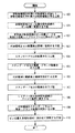
以下、本発明の実施の形態について図面を参照して説明する。図1は本発明の一実施の形態に係る矩形LSI自動レイアウトツールを用いた非矩形LSIレイアウト方法を示すフローチャートである。また、図2から図11は、図1に示すフローチャートの各工程に対応するLSIレイアウトの様子を説明する図である。
【0014】
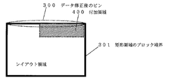
図1において、工程100はレイアウト対象の非矩形領域の外側に付加領域を付加して非矩形領域を含む最小の矩形領域を得る工程である。工程100について図2から図4を用いて説明する。図2はレイアウト対象の非矩形領域を示し、非矩形領域のブロック境界202を有する。図3は図2の非矩形領域を含む最小の矩形領域を示し、矩形領域のブロック境界301を有する。図4には、ブロック境界202を有する非矩形領域からブロック境界301を有する矩形領域を得るために、非矩形領域のブロック境界202の外側に付加した付加領域400を示す。
【0015】
工程101は、工程100で付加した付加領域に接する非矩形領域のピン位置を矩形領域のピン位置に変更する工程である。工程101について図2から図4を用いて説明する。図2において、200は付加領域400に接していないため変更が不要なピン位置を示し、201は付加領域400に接しているため変更の対象となるピン位置を示す。図3において、300はピン位置を変更した後の矩形領域のピン位置を示す。矩形LSI自動レイアウトツールは矩形領域のデータのみ認識可能なので、工程102で、変更により得られた矩形領域のピン位置データを矩形LSI自動レイアウトツールに読み込ませる。
【0016】
工程103は、工程100で付加した付加領域をセル配置禁止領域とする工程である。工程103について図4および図5を用いて説明する。図4の付加領域400は実際のレイアウト対象の非矩形領域に存在しない領域であるので、付加領域400をスタンダードセルの配置禁止領域500として指定する。
【0017】
工程104は矩形領域にスタンダードセルの配置を行う工程である。工程104について図5に示すスタンダードセルの配置図を用いて説明する。工程103で付加領域400がスタンダードセルの配置禁止領域500として指定されているので、工程104によりスタンダードセルの配置を行うと、スタンダードセル501は非矩形領域のブロック境界202の形状に合わせて配置される。ただし矩形LSI自動レイアウトツールはレイアウト形状を矩形領域のブロック境界301で認識しているため、非矩形領域のブロック境界202は認識していない。
【0018】
工程105はスタンダードセルの電源・グランド配線を行う工程である。105の工程について図6に示すスタンダードセルの電源・グランド接続図を用いて説明する。図6において、スタンダードセル用にあらかじめ固定パターンとして設定された電源・グランド配線600により、スタンダードセルの電源およびグランドを配線が行われる。図6においては、電源・グランド配線が機械的に行われた結果、スタンダードセルの配置禁止領域500にも電源・グランド配線が行われる場合を示している。
【0019】
工程106は付加領域に配線禁止領域を指定する工程である。106の工程について図7に示すスタンダードセルの配線禁止領域の指定図を用いて説明する。付加領域400は実際のレイアウト対象の非矩形領域に存在しない領域であるので、配線禁止領域に指定しなければならないが、工程101においてピン位置201がピン位置300に変更されているので、ピン位置300には配線されなければならない。
【0020】
工程106においては、図7に示すように、ピン位置201からピン位置300に変更されたN本のピンについて、ピン位置201とピン位置300の対応するそれぞれのピンを結ぶN本の配線のみを可能にするように、付加領域400上にスタンダードセルの配線禁止領域700を互いに間隔を空けてN+1個指定する。図7において、スタンダードセルの配線禁止領域700を隔てるN個の配線領域701は、それぞれ1本の配線のみが可能なように幅が設定される領域である。
【0021】
工程107はスタンダードセルの配線を行う工程である。工程107について図8を用いて説明する。工程107でスタンダードセルの配線を行うと、矩形LSI自動レイアウトツールはレイアウト形状を矩形領域のブロック境界301で認識して配線を行うが、工程106で付加領域400上にスタンダードセルの配線禁止領域701が指定されているので、結果的として、スタンダードセルの配線802は非矩形領域のブロック境界202の形状に合わせて配線される。また、工程101でピン位置201から変更されたピン位置300の各ピンに対しては、変更前のそれぞれのピン位置201を経由し、それぞれ配線領域701を通して配線が行われる。
【0022】
工程108は矩形領域のブロック境界を非矩形領域のブロック境界に変更する工程である。工程108について図9を用いて説明する。工程107まではスタンダードセルの配置および配線の自動レイアウト処理を行うために、矩形LSI自動レイアウトツールにレイアウト形状を矩形領域のブロック境界301で認識させる必要があったが、自動レイアウト処理が終了したことにより、工程108ではレイアウト形状を元の非矩形領域のブロック境界202に戻す。図9は矩形領域のブロック境界301を非矩形領域のブロック境界202に戻す変更を行った図である。
【0023】
工程109は付加領域に残されたスタンダードセルの電源・グランド配線を削除する工程である。109の工程について図10を用いて説明する。図10は工程105でスタンダードセルの電源・グランド配線が付加領域にも適用された場合を示す図であり、冗長な電源・グランド配線1001は削除されなければならない。工程109において冗長な電源・グランド配線1001が削除されると、スタンダードセルの電源・グランド配線600が残る領域はブロック境界202で示される非矩形領域と一致する。
【0024】
工程110は、工程101においてピン位置201からピン位置300に変更されたピン位置を、非矩形領域のブロック境界に合わせて元のピン位置に戻す工程である。工程110について図11を用いて説明する。図11において、ピン位置1101はピン位置300のうち工程101でピン位置201から変更された部分である。工程109において、工程107で配線領域701を通してピン位置1101に配線された配線部分を削除することにより、非矩形領域内からピン位置201までの配線が残り、ピン位置1101を非矩形領域のブロック境界の元のピン位置201に移動させることができる。
【0025】
以上のように本実施の形態によれば、非矩形領域に付加領域を付加して矩形領域を得る手順と、矩形領域に合わせてピン位置を変更する手順と、付加領域に対してスタンダードセルの配置禁止領域および配線禁止領域を指定する手順と、スタンダードセルの自動レイアウト処理後に不要な部分を削除する手順とを加えることにより、矩形LSI自動レイアウトツールを用いて非矩形レイアウトを行うことができる。
【0026】
【発明の効果】
以上説明したように、本発明によれば、非矩形領域に付加領域を付加し矩形領域を得ることにより、矩形LSI自動レイアウトツールに対して非矩形領域データを矩形領域データとして認識させ、付加領域に対してスタンダードセルの配置禁止領域および配線禁止領域を指定することにより、付加領域にスタンダードセルの不要な配置配線が行われることを避けることができ、矩形LSI自動レイアウトツールを用いて非矩形レイアウトを実現することが可能になる。
【図面の簡単な説明】
【図1】本発明の一実施の形態に係る矩形LSI自動レイアウトツールを用いた非矩形LSIレイアウト方法を示すフローチャート。
【図2】非矩形領域とそのピン位置を説明する図。
【図3】矩形領域とそのピン位置を説明する図。
【図4】付加領域とそのピン位置を説明する図。
【図5】スタンダードセルの配置禁止領域とスタンダードセルの配置を説明する図。
【図6】スタンダードセルの電源・グランドピン接続図。
【図7】スタンダードセルの配線禁止領域の指定を説明する図。
【図8】スタンダードセルの配線図。
【図9】矩形領域から非矩形領域へのブロック境界の変更を説明する図。
【図10】スタンダードセルの電源・グランド配線の削除を説明する図。
【図11】矩形領域から非矩形領域へのピン位置の変更を説明する図。
【符号の説明】
200 変更が不要な非矩形領域のピン位置
201 変更が必要な非矩形領域のピン位置
202 非矩形領域のブロック境界
300 変更後の矩形領域のピン位置
301 矩形領域のブロック境界
400 付加領域
500 スタンダードセルの配置禁止領域
501 スタンダードセル
600 スタンダードセルの電源・グランド配線
700 スタンダードセルの配線禁止領域
701 1本の配線が可能な配線領域
802 スタンダードセルの配線
1001 削除するスタンダードセルの電源・グランド配線
1101 工程101で変更された矩形領域のピン位置[0001]
BACKGROUND OF THE INVENTION
The present invention relates to a non-rectangular layout method performed using a rectangular LSI automatic layout tool.
[0002]
[Prior art]
As an indispensable technology that has supported the development of large-scale integrated circuits (LSIs) in recent years, there is an automatic design technology. Layout design that places and routes semiconductor circuit cells on a wafer based on circuit design as one stage of LSI design is critical for determining the success or failure of LSI design because the resulting chip size directly affects LSI cost. It is an important step. Therefore, in the automatic layout design, ingenuity has been made to collect the layout area into as small a rectangle as possible so that LSI can be extracted from the wafer without waste.
[0003]
In digital LSI, a technique for designing an LSI using a group of standard cells as semiconductor circuit cells has been established. Further, in large-scale LSI development, a method of designing a designed LSI layout as one LSI block and combining such an LSI block or memory circuit block with a standard cell is common.
[0004]
In an analog LSI, unlike a digital circuit design that can be described in binary logic, a design method similar to a digital LSI design using standard cells is not necessarily advantageous from the viewpoint of total cost including development costs. Rather, in recent years, LSI applications in various fields are overwhelmingly demanded for hybrid LSIs that combine analog functions with digital LSIs, so one analog function is separately designed as one LSI block. A method of designing these analog LSI blocks in combination with standard cells together with other LSI blocks has become common.
[0005]
[Problems to be solved by the invention]
In the design of such a hybrid LSI, the layout shape of the LSI block is given in advance, and this and the automatic design block using standard cells must be combined into one chip. However, since analog LSI blocks are designed with priority given to the consideration of analog electrical characteristics, they do not necessarily have a convenient shape for combination with a digital automatic layout.
[0006]
Even in such a case, the conventional digital LSI automatic layout tool is a rectangular target tool. Therefore, when LSI blocks that do not perform automatic layout in LSI design occupy most of the chip, the layout is performed. There is a possibility that useless empty space may occur between LSI blocks.
[0007]
On the other hand, it is conceivable to perform digital automatic layout in a non-rectangular form. However, since the LSI automatic layout tool that has been used in the past only targets the rectangular layout shape, even if an attempt is made to implement a non-rectangular layout. The input data necessary for layout cannot be read.
[0008]
The present invention solves the above-described conventional problems, and it is possible to use a rectangular LSI automatic layout tool for the layout of a non-rectangular LSI block using standard cells, thereby generating unnecessary empty space in the LSI layout. An object of the present invention is to provide a non-rectangular LSI layout method that can eliminate the problem.
[0009]
[Means for Solving the Problems]
In the non-rectangular LSI layout method according to claim 1 of the present invention, a step of obtaining a minimum rectangular region including the non-rectangular region by adding an additional region circumscribing the block boundary of the non-rectangular region to be laid out (100) ), Changing the pin position of the non-rectangular area in contact with the additional area to the pin position of the rectangular area in contact with the additional area, and making the additional area a cell placement prohibited area (103) And (104) performing cell placement using the rectangular area as a layout area, and in the additional area, corresponding pins of the pin position before the non-rectangular area change and the pin position after the rectangular area change. A step (106) of providing a wiring prohibition region excluding a wiring region that enables only wiring to be connected, and a step of wiring using the rectangular region as a layout region ( 07), a step (108) of changing a block boundary of the layout area from the rectangular area to the non-rectangular area after layout of the rectangular area, and a pin position of the rectangular area after the layout of the rectangular area. And a step (110) of returning to the pin position of the non-rectangular LSI using the rectangular LSI automatic layout tool.
[0010]
According to the non-rectangular LSI layout method of claim 1, a rectangular area is obtained by adding an additional area to the non-rectangular area to be laid out, and the pin position is changed in accordance with the rectangular area, and a cell is added to the additional area. By designating the layout prohibition or wiring prohibition area, the rectangular LSI automatic layout tool can recognize the non-rectangular area as the rectangular area, and the layout of the non-rectangular LSI block is performed using the rectangular LSI automatic layout tool. It becomes possible.
[0011]
An LSI layout method according to a second aspect of the present invention is the non-rectangular LSI layout method according to the first aspect, wherein when the cell power supply and ground wiring are laid out in the additional area, the additional area is laid out after the rectangular area is laid out. This includes a step (109) of deleting the power supply and ground wiring of the cell in the area.
[0012]
According to a non-rectangular LSI layout method according to claim 2, in the non-rectangular LSI layout method according to claim 1, when cell power and ground wirings are laid out in an additional area, the addition is performed after the rectangular area is laid out. The power supply and ground wiring of the cells in the area can be deleted, and the redundant portion generated when the layout of the non-rectangular LSI block is performed using the rectangular LSI automatic layout tool can be deleted.
[0013]
DETAILED DESCRIPTION OF THE INVENTION
Hereinafter, embodiments of the present invention will be described with reference to the drawings. FIG. 1 is a flowchart showing a non-rectangular LSI layout method using a rectangular LSI automatic layout tool according to an embodiment of the present invention. 2 to 11 are views for explaining the LSI layout corresponding to each step of the flowchart shown in FIG.
[0014]
In FIG. 1,
[0015]
[0016]
[0017]
Step 104 is a step of arranging standard cells in a rectangular area. Step 104 will be described with reference to the standard cell layout shown in FIG. Since the additional area 400 is designated as the standard cell arrangement prohibition area 500 in
[0018]
Step 105 is a step of performing power supply / ground wiring of the standard cell. The
[0019]
Step 106 is a step of designating a wiring prohibited area as the additional area. The
[0020]
In
[0021]
Step 107 is a step of wiring standard cells. Step 107 will be described with reference to FIG. When the standard cell wiring is performed in
[0022]
Step 108 is a step of changing the block boundary of the rectangular area to the block boundary of the non-rectangular area. Step 108 will be described with reference to FIG. Up to step 107, in order to perform standard cell placement and wiring automatic layout processing, it was necessary for the rectangular LSI automatic layout tool to recognize the layout shape at the
[0023]
Step 109 is a step of deleting the power / ground wiring of the standard cell remaining in the additional region. Step 109 will be described with reference to FIG. FIG. 10 is a diagram showing a case where the power / ground wiring of the standard cell is also applied to the additional region in
[0024]
Step 110 is a step of returning the pin position changed from the pin position 201 to the pin position 300 in
[0025]
As described above, according to the present embodiment, a procedure for obtaining a rectangular area by adding an additional area to a non-rectangular area, a procedure for changing the pin position according to the rectangular area, A non-rectangular layout can be performed using the rectangular LSI automatic layout tool by adding a procedure for designating the placement prohibited area and the wiring prohibited area and a procedure for deleting unnecessary portions after the automatic layout processing of the standard cell.
[0026]
【The invention's effect】
As described above, according to the present invention, by adding an additional area to the non-rectangular area to obtain a rectangular area, the rectangular LSI automatic layout tool is made to recognize the non-rectangular area data as rectangular area data, and the additional area By designating the standard cell placement prohibition area and the wiring prohibition area, it is possible to avoid unnecessary placement and routing of the standard cell in the additional area, and the non-rectangular layout using the rectangular LSI automatic layout tool. Can be realized.
[Brief description of the drawings]
FIG. 1 is a flowchart showing a non-rectangular LSI layout method using a rectangular LSI automatic layout tool according to an embodiment of the present invention.
FIG. 2 is a diagram for explaining a non-rectangular region and its pin position.
FIG. 3 is a diagram illustrating a rectangular area and its pin position.
FIG. 4 is a diagram for explaining an additional region and its pin position.
FIG. 5 is a diagram for explaining an arrangement prohibition area of standard cells and an arrangement of standard cells;
FIG. 6 is a power cell / ground pin connection diagram of a standard cell.
FIG. 7 is a view for explaining designation of a wiring prohibited area of a standard cell.
FIG. 8 is a wiring diagram of a standard cell.
FIG. 9 is a diagram for explaining a block boundary change from a rectangular area to a non-rectangular area.
FIG. 10 is a diagram for explaining deletion of a power supply / ground wiring of a standard cell.
FIG. 11 is a diagram illustrating a change in pin position from a rectangular area to a non-rectangular area.
[Explanation of symbols]
200 Pin position 201 of non-rectangular area that does not need to be changed
Claims (2)
レイアウト対象の非矩形領域のブロック境界に外接する付加領域を付加することにより前記非矩形領域を内包する最小の矩形領域を得る工程と、
前記付加領域に接する前記非矩形領域のピン位置を前記付加領域に接する前記矩形領域のピン位置に変更する工程と、
前記付加領域をセル配置禁止領域とする工程と、
前記矩形領域をレイアウト領域としてセル配置を行う工程と、
前記付加領域において前記非矩形領域の変更前のピン位置と前記矩形領域の変更後のピン位置とのそれぞれ対応するピンを結ぶ配線のみを可能にする配線領域を除いて配線禁止領域を設ける工程と、
前記矩形領域をレイアウト領域として配線を行う工程と、
前記矩形領域のレイアウト後にレイアウト領域のブロック境界を前記矩形領域から前記非矩形領域に変更する工程と、
前記矩形領域のレイアウト後に前記矩形領域のピン位置を前記非矩形領域のピン位置に戻す工程と、
を含むことを特徴とする非矩形LSIレイアウト方法。In a non-rectangular LSI layout method performed using a rectangular LSI automatic layout tool,
Obtaining a minimum rectangular area containing the non-rectangular area by adding an additional area circumscribing the block boundary of the non-rectangular area to be laid out;
Changing the pin position of the non-rectangular area in contact with the additional area to the pin position of the rectangular area in contact with the additional area;
Making the additional region a cell placement prohibited region;
Performing cell placement using the rectangular area as a layout area;
A step of providing a wiring prohibition area in the additional area, except for a wiring area that enables only a wiring connecting pins corresponding to the pin position before the change of the non-rectangular area and the pin position after the change of the rectangular area; ,
Wiring the rectangular region as a layout region;
Changing the block boundary of the layout area from the rectangular area to the non-rectangular area after the layout of the rectangular area;
Returning the pin position of the rectangular area to the pin position of the non-rectangular area after the layout of the rectangular area;
A non-rectangular LSI layout method comprising:
Priority Applications (1)
| Application Number | Priority Date | Filing Date | Title |
|---|---|---|---|
| JP2001122996A JP3611202B2 (en) | 2001-04-20 | 2001-04-20 | Non-rectangular LSI layout method |
Applications Claiming Priority (1)
| Application Number | Priority Date | Filing Date | Title |
|---|---|---|---|
| JP2001122996A JP3611202B2 (en) | 2001-04-20 | 2001-04-20 | Non-rectangular LSI layout method |
Publications (2)
| Publication Number | Publication Date |
|---|---|
| JP2002319622A JP2002319622A (en) | 2002-10-31 |
| JP3611202B2 true JP3611202B2 (en) | 2005-01-19 |
Family
ID=18972619
Family Applications (1)
| Application Number | Title | Priority Date | Filing Date |
|---|---|---|---|
| JP2001122996A Expired - Fee Related JP3611202B2 (en) | 2001-04-20 | 2001-04-20 | Non-rectangular LSI layout method |
Country Status (1)
| Country | Link |
|---|---|
| JP (1) | JP3611202B2 (en) |
-
2001
- 2001-04-20 JP JP2001122996A patent/JP3611202B2/en not_active Expired - Fee Related
Also Published As
| Publication number | Publication date |
|---|---|
| JP2002319622A (en) | 2002-10-31 |
Similar Documents
| Publication | Publication Date | Title |
|---|---|---|
| KR102358571B1 (en) | Integrated circuit and standard cell library | |
| US5231590A (en) | Technique for modifying an integrated circuit layout | |
| JP3822009B2 (en) | AUTOMATIC DESIGN METHOD, EXPOSURE MASK SET, SEMICONDUCTOR INTEGRATED CIRCUIT DEVICE, SEMICONDUCTOR INTEGRATED CIRCUIT DEVICE MANUFACTURING METHOD, AND RECORDING MEDIUM CONTAINING AUTOMATIC DESIGN PROGRAM | |
| US7137094B2 (en) | Method for reducing layers revision in engineering change order | |
| JPS63245940A (en) | Block disposition processing system | |
| JP4254059B2 (en) | Semiconductor integrated circuit design method | |
| US6414852B1 (en) | Integrated circuit and method of design thereof | |
| JP2001306641A (en) | Automatic arranging and wiring method for semiconductor integrated circuit | |
| JP3611202B2 (en) | Non-rectangular LSI layout method | |
| US6780745B2 (en) | Semiconductor integrated circuit and method of manufacturing the same | |
| JP3647686B2 (en) | Semiconductor integrated circuit design method and semiconductor integrated circuit manufacturing method | |
| JP2910734B2 (en) | Layout method | |
| US7698675B2 (en) | Method and design system for semiconductor integrated circuit with a reduced placement area | |
| JP4248925B2 (en) | Automatic floor plan determination method | |
| JP3204381B2 (en) | Automatic placement and routing of semiconductor devices | |
| US20030023946A1 (en) | Standard cell library generation using merged power method | |
| JP2912300B2 (en) | ASIC layout method | |
| JP3651654B2 (en) | Functional macro, design method thereof, and design method of semiconductor device | |
| US7992118B2 (en) | Semiconductor integrated circuit and design method for semiconductor integrated circuit | |
| JP2001358223A (en) | Method of designing lsi circuit using hard blocks and method of restoring cell-placement information of hard blocks for lsi | |
| JP2620005B2 (en) | Placement and wiring decision method | |
| JPH06216249A (en) | Automatic layout design system for ic chip | |
| JP2580982B2 (en) | LSI power supply wiring layout system | |
| JP2002134621A (en) | Method for synthesizing mask data, method for inspecting mask data, and semiconductor integrated device | |
| JPH0221634A (en) | Mask layout method for semiconductor integrated circuit |
Legal Events
| Date | Code | Title | Description |
|---|---|---|---|
| A977 | Report on retrieval |
Free format text: JAPANESE INTERMEDIATE CODE: A971007 Effective date: 20040827 |
|
| TRDD | Decision of grant or rejection written | ||
| A01 | Written decision to grant a patent or to grant a registration (utility model) |
Free format text: JAPANESE INTERMEDIATE CODE: A01 Effective date: 20041013 |
|
| A61 | First payment of annual fees (during grant procedure) |
Free format text: JAPANESE INTERMEDIATE CODE: A61 Effective date: 20041014 |
|
| R150 | Certificate of patent or registration of utility model |
Free format text: JAPANESE INTERMEDIATE CODE: R150 |
|
| FPAY | Renewal fee payment (event date is renewal date of database) |
Free format text: PAYMENT UNTIL: 20071029 Year of fee payment: 3 |
|
| FPAY | Renewal fee payment (event date is renewal date of database) |
Free format text: PAYMENT UNTIL: 20081029 Year of fee payment: 4 |
|
| FPAY | Renewal fee payment (event date is renewal date of database) |
Free format text: PAYMENT UNTIL: 20091029 Year of fee payment: 5 |
|
| FPAY | Renewal fee payment (event date is renewal date of database) |
Free format text: PAYMENT UNTIL: 20091029 Year of fee payment: 5 |
|
| FPAY | Renewal fee payment (event date is renewal date of database) |
Free format text: PAYMENT UNTIL: 20101029 Year of fee payment: 6 |
|
| LAPS | Cancellation because of no payment of annual fees |