JP3600228B2 - Optical scanning device and image forming apparatus - Google Patents
Optical scanning device and image forming apparatus Download PDFInfo
- Publication number
- JP3600228B2 JP3600228B2 JP2002295220A JP2002295220A JP3600228B2 JP 3600228 B2 JP3600228 B2 JP 3600228B2 JP 2002295220 A JP2002295220 A JP 2002295220A JP 2002295220 A JP2002295220 A JP 2002295220A JP 3600228 B2 JP3600228 B2 JP 3600228B2
- Authority
- JP
- Japan
- Prior art keywords
- scanning
- light
- optical
- scanned
- image
- Prior art date
- Legal status (The legal status is an assumption and is not a legal conclusion. Google has not performed a legal analysis and makes no representation as to the accuracy of the status listed.)
- Expired - Fee Related
Links
Images


Classifications
-
- B—PERFORMING OPERATIONS; TRANSPORTING
- B41—PRINTING; LINING MACHINES; TYPEWRITERS; STAMPS
- B41J—TYPEWRITERS; SELECTIVE PRINTING MECHANISMS, i.e. MECHANISMS PRINTING OTHERWISE THAN FROM A FORME; CORRECTION OF TYPOGRAPHICAL ERRORS
- B41J2/00—Typewriters or selective printing mechanisms characterised by the printing or marking process for which they are designed
- B41J2/435—Typewriters or selective printing mechanisms characterised by the printing or marking process for which they are designed characterised by selective application of radiation to a printing material or impression-transfer material
- B41J2/47—Typewriters or selective printing mechanisms characterised by the printing or marking process for which they are designed characterised by selective application of radiation to a printing material or impression-transfer material using the combination of scanning and modulation of light
- B41J2/471—Typewriters or selective printing mechanisms characterised by the printing or marking process for which they are designed characterised by selective application of radiation to a printing material or impression-transfer material using the combination of scanning and modulation of light using dot sequential main scanning by means of a light deflector, e.g. a rotating polygonal mirror
- B41J2/473—Typewriters or selective printing mechanisms characterised by the printing or marking process for which they are designed characterised by selective application of radiation to a printing material or impression-transfer material using the combination of scanning and modulation of light using dot sequential main scanning by means of a light deflector, e.g. a rotating polygonal mirror using multiple light beams, wavelengths or colours
-
- G—PHYSICS
- G02—OPTICS
- G02B—OPTICAL ELEMENTS, SYSTEMS OR APPARATUS
- G02B26/00—Optical devices or arrangements for the control of light using movable or deformable optical elements
- G02B26/08—Optical devices or arrangements for the control of light using movable or deformable optical elements for controlling the direction of light
- G02B26/10—Scanning systems
- G02B26/12—Scanning systems using multifaceted mirrors
- G02B26/123—Multibeam scanners, e.g. using multiple light sources or beam splitters
-
- H—ELECTRICITY
- H04—ELECTRIC COMMUNICATION TECHNIQUE
- H04N—PICTORIAL COMMUNICATION, e.g. TELEVISION
- H04N1/00—Scanning, transmission or reproduction of documents or the like, e.g. facsimile transmission; Details thereof
- H04N1/04—Scanning arrangements, i.e. arrangements for the displacement of active reading or reproducing elements relative to the original or reproducing medium, or vice versa
- H04N1/047—Detection, control or error compensation of scanning velocity or position
- H04N1/0473—Detection, control or error compensation of scanning velocity or position in subscanning direction, e.g. picture start or line-to-line synchronisation
-
- H—ELECTRICITY
- H04—ELECTRIC COMMUNICATION TECHNIQUE
- H04N—PICTORIAL COMMUNICATION, e.g. TELEVISION
- H04N1/00—Scanning, transmission or reproduction of documents or the like, e.g. facsimile transmission; Details thereof
- H04N1/04—Scanning arrangements, i.e. arrangements for the displacement of active reading or reproducing elements relative to the original or reproducing medium, or vice versa
- H04N1/113—Scanning arrangements, i.e. arrangements for the displacement of active reading or reproducing elements relative to the original or reproducing medium, or vice versa using oscillating or rotating mirrors
-
- H—ELECTRICITY
- H04—ELECTRIC COMMUNICATION TECHNIQUE
- H04N—PICTORIAL COMMUNICATION, e.g. TELEVISION
- H04N1/00—Scanning, transmission or reproduction of documents or the like, e.g. facsimile transmission; Details thereof
- H04N1/40—Picture signal circuits
- H04N1/40006—Compensating for the effects of ageing, i.e. changes over time
-
- H—ELECTRICITY
- H04—ELECTRIC COMMUNICATION TECHNIQUE
- H04N—PICTORIAL COMMUNICATION, e.g. TELEVISION
- H04N1/00—Scanning, transmission or reproduction of documents or the like, e.g. facsimile transmission; Details thereof
- H04N1/40—Picture signal circuits
- H04N1/401—Compensating positionally unequal response of the pick-up or reproducing head
- H04N1/4015—Compensating positionally unequal response of the pick-up or reproducing head of the reproducing head
-
- H—ELECTRICITY
- H04—ELECTRIC COMMUNICATION TECHNIQUE
- H04N—PICTORIAL COMMUNICATION, e.g. TELEVISION
- H04N1/00—Scanning, transmission or reproduction of documents or the like, e.g. facsimile transmission; Details thereof
- H04N1/04—Scanning arrangements, i.e. arrangements for the displacement of active reading or reproducing elements relative to the original or reproducing medium, or vice versa
- H04N1/113—Scanning arrangements, i.e. arrangements for the displacement of active reading or reproducing elements relative to the original or reproducing medium, or vice versa using oscillating or rotating mirrors
- H04N1/1135—Scanning arrangements, i.e. arrangements for the displacement of active reading or reproducing elements relative to the original or reproducing medium, or vice versa using oscillating or rotating mirrors for the main-scan only
-
- H—ELECTRICITY
- H04—ELECTRIC COMMUNICATION TECHNIQUE
- H04N—PICTORIAL COMMUNICATION, e.g. TELEVISION
- H04N1/00—Scanning, transmission or reproduction of documents or the like, e.g. facsimile transmission; Details thereof
- H04N1/04—Scanning arrangements, i.e. arrangements for the displacement of active reading or reproducing elements relative to the original or reproducing medium, or vice versa
- H04N1/12—Scanning arrangements, i.e. arrangements for the displacement of active reading or reproducing elements relative to the original or reproducing medium, or vice versa using the sheet-feed movement or the medium-advance or the drum-rotation movement as the slow scanning component, e.g. arrangements for the main-scanning
-
- H—ELECTRICITY
- H04—ELECTRIC COMMUNICATION TECHNIQUE
- H04N—PICTORIAL COMMUNICATION, e.g. TELEVISION
- H04N1/00—Scanning, transmission or reproduction of documents or the like, e.g. facsimile transmission; Details thereof
- H04N1/04—Scanning arrangements, i.e. arrangements for the displacement of active reading or reproducing elements relative to the original or reproducing medium, or vice versa
- H04N1/19—Scanning arrangements, i.e. arrangements for the displacement of active reading or reproducing elements relative to the original or reproducing medium, or vice versa using multi-element arrays
- H04N1/191—Scanning arrangements, i.e. arrangements for the displacement of active reading or reproducing elements relative to the original or reproducing medium, or vice versa using multi-element arrays the array comprising a one-dimensional array, or a combination of one-dimensional arrays, or a substantially one-dimensional array, e.g. an array of staggered elements
- H04N1/192—Simultaneously or substantially simultaneously scanning picture elements on one main scanning line
-
- H—ELECTRICITY
- H04—ELECTRIC COMMUNICATION TECHNIQUE
- H04N—PICTORIAL COMMUNICATION, e.g. TELEVISION
- H04N2201/00—Indexing scheme relating to scanning, transmission or reproduction of documents or the like, and to details thereof
- H04N2201/024—Indexing scheme relating to scanning, transmission or reproduction of documents or the like, and to details thereof deleted
- H04N2201/02406—Arrangements for positioning elements within a head
- H04N2201/02439—Positioning method
- H04N2201/02441—Positioning method using screws
-
- H—ELECTRICITY
- H04—ELECTRIC COMMUNICATION TECHNIQUE
- H04N—PICTORIAL COMMUNICATION, e.g. TELEVISION
- H04N2201/00—Indexing scheme relating to scanning, transmission or reproduction of documents or the like, and to details thereof
- H04N2201/04—Scanning arrangements
- H04N2201/047—Detection, control or error compensation of scanning velocity or position
- H04N2201/04701—Detection of scanning velocity or position
- H04N2201/04715—Detection of scanning velocity or position by detecting marks or the like, e.g. slits
- H04N2201/04722—Detection of scanning velocity or position by detecting marks or the like, e.g. slits on a photoconductive drum or belt
-
- H—ELECTRICITY
- H04—ELECTRIC COMMUNICATION TECHNIQUE
- H04N—PICTORIAL COMMUNICATION, e.g. TELEVISION
- H04N2201/00—Indexing scheme relating to scanning, transmission or reproduction of documents or the like, and to details thereof
- H04N2201/04—Scanning arrangements
- H04N2201/047—Detection, control or error compensation of scanning velocity or position
- H04N2201/04701—Detection of scanning velocity or position
- H04N2201/04732—Detecting at infrequent intervals, e.g. once or twice per line for main-scan control
-
- H—ELECTRICITY
- H04—ELECTRIC COMMUNICATION TECHNIQUE
- H04N—PICTORIAL COMMUNICATION, e.g. TELEVISION
- H04N2201/00—Indexing scheme relating to scanning, transmission or reproduction of documents or the like, and to details thereof
- H04N2201/04—Scanning arrangements
- H04N2201/047—Detection, control or error compensation of scanning velocity or position
- H04N2201/04753—Control or error compensation of scanning position or velocity
- H04N2201/04758—Control or error compensation of scanning position or velocity by controlling the position of the scanned image area
- H04N2201/04787—Control or error compensation of scanning position or velocity by controlling the position of the scanned image area by changing or controlling the addresses or values of pixels, e.g. in an array, in a memory, by interpolation
-
- H—ELECTRICITY
- H04—ELECTRIC COMMUNICATION TECHNIQUE
- H04N—PICTORIAL COMMUNICATION, e.g. TELEVISION
- H04N2201/00—Indexing scheme relating to scanning, transmission or reproduction of documents or the like, and to details thereof
- H04N2201/04—Scanning arrangements
- H04N2201/047—Detection, control or error compensation of scanning velocity or position
- H04N2201/04753—Control or error compensation of scanning position or velocity
- H04N2201/04794—Varying the control or compensation during the scan, e.g. using continuous feedback or from line to line
- H04N2201/04796—Varying the sub-scan control during the main-scan, e.g. for correcting skew, tilt or bow of a scanning beam
Description
【0001】
【発明の属する技術分野】
この発明は光走査装置および画像形成装置に関する。
【0002】
【従来の技術】
画像データに基づき変調された光源からの光束を、回転多面鏡等の「光偏向走査手段」により主走査方向に偏向し、偏向光束をfθレンズ等の「走査結像光学系」により被走査面に向けて集光し、被走査面上に光スポットを形成し、光スポットにより被走査面を光走査する光走査装置は、光プリンタや光プロッタ、デジタル複写機等の画像形成装置に関連して広く知られている。
【0003】
光走査装置を用いる画像形成装置では一般に「光走査により画像の書込みを行う画像書込工程を含む画像形成プロセス」が実行されるが、形成される画像の良否は光走査の良否にかかっている。光走査の良否は、光走査装置の「主走査方向や副走査方向の走査特性」に依存する。
【0004】
主走査方向の走査特性としては例えば、光走査の等速特性がある。
例えば、光偏向走査手段として回転多面鏡を用いる場合、光束の偏向は等角速度的に行われるので、光走査の等速特性を実現するために、走査結像光学系としてfθ特性を持つものを用いている。しかしながら、走査結像光学系に要請される他の性能との関係もあって、完全なfθ特性を実現することは容易でない。このため、現実の光走査においては、光走査が完全に等速的に行われることは無く、走査特性としての等速特性は「理想の等速走査からのずれ」を伴っている。
【0005】
主走査方向の走査特性はまた、fθ特性が十分補正されていない場合以外にも、光走査光学系の光学部品精度・ハウジングへの取付精度の劣化や、光走査装置内の温度・湿度などの環境変動による光学部品の特性変動、被走査面の実態をなす感光体や中間転写体の回転軸方向のぶれ等にも起因して生じる。
【0006】
副走査方向の走査特性には「走査線曲がり」や「走査線の傾き」がある。走査線は「被走査面上における光スポットの移動軌跡」で、直線であることが理想であり、光走査装置の設計も走査線が直線となるように行われるが、実際には、加工誤差や組立誤差等が原因して走査線の曲がりが発生するのが普通である。このような走査線の曲がりを「走査線曲がり」と呼び、その曲がり具合を「走査線曲がり特性」と呼ぶ。
【0007】
走査結像光学系として「結像ミラー」を用い、偏向光束の、結像ミラーへの入射方向と反射方向との間に、副走査方向で角度を持たせる場合には、原理的に走査線曲がりが発生するし、走査結像光学系をレンズ系として構成する場合でも、被走査面を「副走査方向に分離した複数の光スポットで光走査」するマルチビーム走査方式では走査線曲がりが不可避的である。
【0008】
「走査線の傾き」は、走査線が副走査方向に対して正しく直交しない現象で、走査線曲がりの1種である。従って、以下の説明においては特に断らない限り、「走査線の傾き」は走査線曲がりに含めて説明する。
【0009】
光走査の等速特性が完全でないと、形成された画像に主走査方向の歪みが生じ、走査線曲がりは、形成された画像に副走査方向の歪みを生じさせる。画像がモノクロームで、単一の光走査装置により書込み形成される場合は、走査線曲がりや等速特性の不完全さ(理想の等速走査からのずれ)がある程度抑えられていれば、形成された画像に「目視で分かるほどの歪み」は生じないが、それでも、このような画像の歪みは少ないに越したことは無い。
【0010】
モノクロームの画像であっても、CAD(コンピュータ支援デザイン)の出力等で、画像における直線性が重視されるような場合には、僅かな走査線曲がりでも出力された画像の品質を著しく劣化させることになり、無視できない問題となる。
【0011】
マゼンタ・シアン・イエローの3色、あるいはこれに黒を加えた4色の画像を色成分画像として形成し、これらの色成分画像を重ね合せることにより合成的にカラー画像を形成することは、従来から、カラー複写機等で行われている。
【0012】
このようなカラー画像形成を行うのに、各色の成分画像を異なる光走査装置で異なる感光体に形成する所謂「タンデム型」と呼ばれる画像形成方式があるが、このような画像形成方式の場合、光走査装置相互で「走査線の曲がり具合や傾きが異なる」と、光走査装置ごとの走査線曲がりが一応の許容範囲内に補正されていたとしても、光走査装置ごとの走査線の僅かな不一致に起因して、形成されたカラー画像に「色ずれ」と呼ばれる画像異常が現れて、カラー画像の画質を劣化させる。
【0013】
また、色ずれ現象の現われ方の1つとして、カラー画像における色合いが所望のものにならないという現象がある。
近来、走査特性の向上を目して、光走査装置の結像光学系に、非球面に代表される特殊な面を採用することが一般化しており、このような特殊な面を容易に形成でき、なおかつコストも安価な「樹脂材料の結像光学系」が多用されている。
【0014】
樹脂材料の結像光学系は、温度や湿度の変化の影響を受けて素子の形状や屈折率等が変化して光学特性が変化しやすく、このような光学特性の変化は「走査線の曲がり具合や等速特性」をも変化させる。そうすると、例えば、数十枚のカラー画像の形成を連続して行う場合に、画像形成装置の連続運転により機内温度が上昇し、結像光学系の光学特性が変化して、各光走査装置の書込む走査線の曲がり具合や等速特性が次第に変化し、色ずれの現象により、初期に得られたカラー画像と、終期に得られたカラー画像とで、色合いが全く異なるものになることがある。
【0015】
請求項2や請求項10以下の発明において行われる「被走査面あるいは被走査領域に、副走査方向において露光分布」を形成することに関しては特許文献1に記載がある。また、「光源の変調駆動タイミングの調整により、走査線位置を副走査方向に調整する」点に関しては特許文献2に記載がある。
【0016】
また、請求項4記載の発明で用いる液晶偏向素子に関連した技術は、特許文献3、4に記載がある。
【0017】
【特許文献1】
特開2001−215437号公報
【特許文献2】
特開2000−235290号公報
【特許文献3】
特開平8−313941号公報(0057)
【特許文献4】
特開平8−313941号公報(0060)
【0018】
【発明が解決しようとする課題】
この発明は、光走査装置において、走査線の曲がりを有効に補正し、良好な光走査を可能とすることを課題とする。
この発明はまた、光走査装置において、走査線の曲がりの補正に加えて、等速特性に起因する「主走査方向の走査位置のずれ」を良好に補正することにより、より良好な光走査を可能とすることを課題とする。
【0019】
さらにこの発明は、画像形成装置に上記光走査装置を用いることにより、光走査による良好な画像形成を可能ならしむることを課題とする。
【0020】
この発明はさらに、複数の被走査領域の光走査を個別的に行う場合に、被走査領域間での相対的な走査線のずれや曲がり・傾きを補正することを課題とする。
【0021】
【課題を解決するための手段】
請求項1記載の光走査装置は「画像データに基づき変調された光源からの光束を光偏向走査手段により主走査方向に偏向し、偏向光束を走査結像光学系により被走査面に向けて集光し、被走査面上に光スポットを形成し、この光スポットにより被走査面を光走査する光走査装置」である。
【0022】
「画像データ」は、光走査により形成しようとする画像の「画素単位のデータの集合」であり、光源から放射される光束は、この画像データに従って強度変調され、画素に応じた被走査面位置に書込みを行う。画像データは「複写しようとする原稿を読取って画素ごとのデータに変換したもの」であることもあるし、コンピュータやワードプロセッサ、デジタルカメラや情報端末装置等で生成されたものである場合もあり、外部データとして転送されるものである場合もある。
【0023】
「光偏向走査手段」は、光源側からの光束を光走査のために主走査方向に偏向させる手段であり、ポリゴンミラーを回転させる回転多面鏡を始め、ピラミダルミラーやホゾ型ミラー等の回転1面鏡や、回転2面鏡あるいはガルバノミラー等、従来から知られた各種のものを用いることができる。
【0024】
「走査結像光学系」は、光偏向走査手段により偏向された光束を被走査面に向けて集光させ、被走査面上に光スポットを形成するための光学系であり、fθレンズ等の「レンズ系」として構成することも、fθミラー等の「結像ミラー系」として構成することもでき、「レンズ系とミラー系の複合系」として構成することもできる。
【0025】
走査結像光学系は「樹脂製結像素子」を含むことができる。この場合、樹脂製結像素子は走査結像光学系の一部を構成しても良いし、走査結像光学系全体が樹脂製結像素子で構成されていてもよい。勿論、単一の樹脂製結像素子が「走査結像光学系自体」を構成することもできる。
【0026】
走査結像光学系は、光スポットによる光走査を等速化する「等速化機能」を有する。例えば、光偏向走査手段による光束の偏向が等角速度的である場合、走査結像光学系として「光スポットによる走査を等速化するためにfθ機能を有するもの」が用いられる。この場合は「fθ特性」が「光走査の等速特性」である。
【0027】
「被走査面」は、光スポットにより光走査される面で、実体としては一般に感光媒体である。
【0028】
「感光媒体」としては種々のものが可能である。例えば、感光媒体として「銀塩フィルム」を用いることができる。この場合、光走査による書込みで潜像が形成されるが、この潜像は通常の銀塩写真プロセスによる処理で可視化することができる。このような感光媒体を用いる画像形成装置は「光製版装置」や、CTスキャン画像等を描画する「光描画装置」として実施できる。
【0029】
感光媒体としてはまた「光走査の際に光スポットの熱エネルギにより発色する発色媒体」を用いることもでき、この場合には、光走査により直接に可視画像を形成できる。
【0030】
感光媒体としてはまた「光導電性の感光体」を用いることができる。光導電性の感光体は、酸化亜鉛紙のようにシート状のものもあるし、セレン感光体や有機光半導体等「ドラム状あるいはベルト状で繰り返し使用されるもの」であることもある。
【0031】
請求項1記載の光走査装置は、以下の如き特徴を有する。
即ち「有効走査領域を、走査線曲がり特性に応じて複数の領域:Di(i=1,2,..)に分割し、各光走査ごとに、複数走査ラインにおける画像データのうちから、各領域:Diの光走査に適した画像データを選択することにより、走査線曲がりに拘わらず、各走査ラインの画像データを、走査線曲がりを補正して書込む分割書込み方式を実行」する。
【0032】
「有効走査領域」は、光スポットが光走査する被走査面上における主走査方向の領域で、画像データの書込みを有効に行い得る領域を言う。
「走査ライン」は、画像上で画像の1ラインを構成するラインを理想化した直線であり、1走査ラインには、このライン上の画像を構成する一連の画像データが書込まれる。
【0033】
請求項1記載の光走査装置では、光スポットが被走査面を1回光走査するごとに、複数の走査ラインの画像データが選択されることにより「複数の走査ラインが、それぞれ部分的に書込ま」れる。従って、1走査ライン全体の画像データは、光スポットによる複数回の光走査で書込まれることになる。
【0034】
このように、請求項1記載の光走査装置では、光スポットによる1回の光走査の際に、複数走査ラインの画像データが分割して書込まれ、また1走査ラインを構成する画像データが、光スポットの複数回の光走査に分割されて行われるので、このような光走査方式を「分割書込み方式」と呼ぶのである。
【0035】
上記請求項1記載の光走査装置の光源は「被走査面上に副走査方向に近接した2以上の光スポットを形成するような複数の光束」を放射することができ、この場合「複数の光束の光強度分布を副走査方向に重畳した合成光強度分布における重心位置」を各光束の強度調整により可変とし、分割書込み方式で補正しきれない1走査ライン内の走査線曲がりを微調補正するようにできる(請求項2)。
【0036】
請求項1記載の光走査装置はまた「光源からの光束を副走査方向に偏向可能な偏向手段」を有することができ、この偏向手段による光束の偏向により、被走査面上における光スポット位置を副走査方向に可変とし、分割書込み方式で補正しきれない1走査ライン内の走査線曲がりを微調補正するように構成できる(請求項3)。
【0037】
請求項3記載の光走査装置における「偏向手段」は、1以上の液晶偏向素子を有することもできるし(請求項4)、「反射面の向きを調整可能な偏向ミラー」を有することもできる(請求項5)。
【0038】
上記請求項1〜5の任意の1に記載の光走査装置は「書込む画像データの画素クロックよりも高い高周波クロックに基づき、画素クロックの位相シフトを行い、光スポット位置を主走査方向に補正的に調整する」ことができる。
【0039】
「光スポット位置を主走査方向に補正的に調整する」とは、被走査面上における光スポットの位置を、各像高ごとに「主走査方向の理想の位置」に合致させ、あるいは近づけるように調整することを意味する。
【0040】
上記請求項1〜6の任意の1に記載の光走査装置は、「偏向光束の光スポットの走査位置を検出する走査位置検出手段」を有することができる。
【0041】
請求項8記載の光走査装置は、以下の点を特徴とする。
即ち、光源から複数の光束を放射させ、これら複数の光束が被走査面上で副走査方向に分離した複数の光スポットを形成し、且つ、各光スポットの走査線曲がり特性が実質的に同一となるようにして、これら複数の光スポットにより被走査面を同時に光走査するようにする。
【0042】
また、有効走査領域を、走査線曲がり特性に応じて複数の領域:Di(i=1,2,..)に分割する。そして「複数の光スポットによる同時の光走査ごと」に、走査ラインごとに上記複数の光束のうちから、各領域:Diの光走査に適した光束を選択することにより、走査線曲がりに拘わらず、各走査ラインの画像データを「走査線曲がりを補正して書込む光束選択書込み方式」を実行する。
【0043】
即ち、光束選択書込み方式は、上に説明した分割書込み方式をマルチビーム化したものである。分割書込み方式では光スポットは1個なので、この光スポットが曲がった走査線を描くのに合わせて、情報を書き込む走査ラインを異ならせるのであるが、請求項8記載の発明のように、被走査面を副走査方向に分離した複数の光スポットで同時に光走査する場合だと、光スポットの数をNとして、同時にN本の走査ラインに対する書込みが可能なので、各光束の光走査に対して上記分割書込み方式を実施すると、各走査ラインは、複数の光束のうちから当該走査ラインの書込みに最も適したものが選択され(この特徴のために「光束選択書込み方式」と呼ばれる)、且つ、一度にN本の走査ラインの書込みが可能となる。
【0044】
この発明の画像形成装置は「光導電性の感光体をN(≧2)個、シート状記録媒体の搬送路に沿って配置し、各感光体に別個の静電潜像を光走査により書込み形成し、各静電潜像を色の異なるトナー画像として可視化し、これらトナー画像を同一のシート状記録媒体上に重ね合せて転写・定着するタンデム式の画像形成装置」であって、以下の如き特徴を有する。
【0045】
即ち、感光体ごとに光走査装置を有し、感光体のうちのひとつには、黒トナー画像が形成される。そして、この黒トナー画像が形成される感光体以外のN−1個の感光体に対する光走査装置は請求項1〜8の任意の1に記載のものであり、黒トナー画像を基準として、走査線曲がり・走査位置の主走査方向の補正のうち、少なくとも、走査線曲がりの補正を行う。
【0046】
上記複数の光走査装置は互いに独立した別個のもので良いが、後述する実施の形態におけるように「光源から被走査面に至る光路上において、一部の光学素子(例えば、光偏向走査手段)を共通化する」ことができる。
【0047】
「光導電性の感光体」は、セレン感光体や有機光半導体等「ドラム状あるいはベルト状で繰り返し使用されるもの」である。静電潜像は、感光体の均一帯電と、光走査装置による光走査により形成される。
【0048】
トナー画像が転写・定着される「シート状記録媒体」は、転写紙やOHPシート(オーバヘッドプロジェクタ用のプラスチックシート)等である。
【0049】
光導電性の感光体からシート状記録媒体へのトナー画像の転写は、感光体からシート状記録媒体へ直接的に転写(直接転写方式)しても良いし、感光体から一旦中間転写ベルト等の中間転写媒体に転写した後、この中間転写媒体からシート状記録媒体へ転写(中間転写方式)するようにしてもよい。
このような画像形成装置は、光カラープリンタや光カラープロッタ、デジタルカラー複写機、カラーファクシミリ装置等として実施できる。
【0050】
以下に参考例として説明する画像形成装置は「複数の光走査手段を用い、複数の被走査領域を光走査し、所望の画像を合成するべき画像を複数の被走査領域に分けて書込む光走査装置」を用いる。上記複数の光走査手段は互いに独立した別個のものでも良いが、後述する実施の形態におけるように「光源から被走査面に至る光路上において、一部の光学素子(例えば、光偏向走査手段)を共通化する」ことができる。
【0051】
「光走査手段」は、変調駆動される光源からの光束を光偏向走査手段により偏向させ、偏向光束を走査結像光学系により導光して被走査面上に光スポットを形成し、この光スポットにより被走査面を光走査する手段である。参考例の画像形成装置は、このような光走査手段が複数用いられ、各光走査手段は「互いに異なる被走査領域」を光走査する。
【0052】
「変調駆動される光源からの光束」は、前述の「画像データに基づき変調された光束」と同義である。「被走査領域」は、実体的には感光性媒体の感光面で、上述した被走査面の概念を含むものであるが、別個の被走査領域は「それぞれ光導電性の感光体」である。
【0053】
参考例の画像形成装置では「少なくとも1つの被走査領域において、副走査方向に隣接する走査線間に重心を有する露光分布を形成し、重心の副走査方向の位置を可変とする」のである。
【0054】
「副走査方向に隣接する走査線間に重心を有する露光分布」は、「被走査領域上で副走査方向に隣接する走査線上に、互いに副走査方向に隣接する2つの光スポットを形成した場合における、これら2つの光スポットの光強度分布を、副走査方向に重畳した合成光強度分布における重心位置が、上記隣接する走査線間にあるもの」を言う。上記2つの光スポットの光強度を相対的に変化させ、一方の光強度を大きく、他方の光強度を小さくすることにより、上記重心の位置を副走査方向に可変にできる。
【0055】
前記請求項2記載の光走査装置では、このように形成される光強度分布の重心位置の調整で「分割書込み方式で補正しきれない1走査ライン内の走査線曲がりを微調補正する」のであるが、参考例の光画像形成装置では、被走査領域内に形成される走査線の長さ全域にわたって、重心位置の調整を行う。
【0056】
参考例の画像形成装置において「副走査方向に隣接する走査線の間に露光分布を形成する被走査領域において、主走査方向に長い1ドットラインを形成する」場合、隣接する走査線の一方から、副走査方向における露光分布の重心までの距離を「主走査方向の位置に応じて異ならせる」ことができ、この場合、主走査方向に長い1ドットラインの主走査方向の位置に応じて「隣接する走査線の一方から、副走査方向における露光分布の重心までの距離を、主走査方向の位置に応じて連続的に変化させる」ことができる。
【0057】
露光分布の重心位置は、主走査方向の位置に従って、副走査方向に段差をなして変化しても良い。即ち、この場合には、露光分布の重心位置は副走査方向に段階的に変位する。
【0058】
参考例の画像形成装置においては「主走査方向に長い1ドットラインを形成するための露光分布の重心位置が、副走査方向に隣接する2つ以上の走査線をまたがって変位可能である」ことができる。
【0059】
ここに露光分布の重心位置が「副走査方向に隣接する2つ以上の走査線をまたがって変位可能」であるとは、以下の如き意味である。
【0060】
即ち、副走査方向に隣接する走査線を、走査線i―1、i、i+1とするとき、走査線i―1上の光スポットと、走査線i上の光スポットとのなす露光分布の重心はこれら光スポットの相対的な光強度の調整により、走査線i―1とi間で変位させることができるが、さらに、走査線iとi+1のそれぞれに形成される光スポットの露光分布の重心は、これら光スポットの相対的な光強度の調整で、走査線iとi+1との間で変位させることができる。
【0061】
このようにして、1本の走査線を書込む間に3以上の走査線上に形成される光スポットの内、隣接する2つの光スポットの光強度を調整することにより、露光分布の重心は「2以上の走査線間(上の例では走査線i―1とiとi+1)」で変位可能である。このような場合を「露光分布の重心が2以上の走査線をまたがって変位する」という。
【0062】
上記参考例の画像形成装置に用いられる光走査装置においては「複数の被走査領域を副走査方向に設定」することができ、このように設定された複数の被走査領域の少なくとも1つにおいて「副走査方向に隣接する走査線間に重心を有する露光分布」を形成し、この重心の副走査方向の位置を変位させることにより、複数の被走査領域相互における副走査方向の相対的な光走査位置を補正することができる。勿論、この場合も「露光分布の重心が2以上の走査線をまたがって変位する」ようにできる。
【0063】
上記参考例の画像形成装置においては「複数の被走査領域を副走査方向に設定し、被走査領域の少なくとも1つにおいて、副走査方向に隣接する走査線間に重心を有する露光分布を形成し、重心の副走査方向の位置を変位させることにより、複数の被走査領域相互における相対的な走査線の曲がりを補正する」ことができる。「走査線の曲がり」は、走査線の傾きを含む。
【0064】
このように、複数の被走査領域を副走査方向に設定することは、例えば、被走査領域の個々を光導電性の感光体とし、これらを副走査方向に並列的に配置することによって実現できる。したがって、上記参考例の画像形成装置は、タンデム型の画像形成装置として実施することができる。
【0065】
副走査方向に設定された被走査領域は、上記の「副走査方向に並列的に配設された感光体」に限らず、同一の感光体の感光面に「異なる画像を書込まれる別個の光走査位置」として設定される場合も含む。
【0066】
参考例の画像形成装置は「少なくとも1つの光走査手段において、光源の変調駆動タイミングの調整により、走査線位置を副走査方向に調整可能」である。
【0067】
「光源の変調駆動タイミングの調整により、走査線位置を副走査方向に調整」するのは以下の如き方法による。
光偏向走査手段として、偏向反射面をn面有する回転多面鏡を考えて見る。この場合、回転多面鏡の回転で各偏向反射面により光束偏向を行わせれば、回転多面鏡の1回転でn本の走査線を光走査できる。例えば、n=6とすれば、回転多面鏡の1回転で6走査線を光走査できる。
【0068】
このような回転多面鏡を用い、偏向反射面に番号を振って1〜6番目の偏向反射面とし、光束の偏向を奇数番目の偏向反射面で行うようにすると、回転多面鏡の1回転ごとに3走査線が光走査される。このとき光源の変調駆動タイミングを調整して、光束の偏向を偶数番目の偏向反射面で行うようにすると、光走査される走査線の位置を、奇数番目の偏向反射面のみを用いて光束を偏向させる場合に対し「副走査方向に走査線ピッチの1/2ピッチ分」だけずらすことができる。
【0069】
一般に、偏向反射面のN面ごとに光束の偏向を行うとすれば、光源の変調駆動タイミングを調整して、光束偏向を行う偏向反射面を1面ずらすようにすると、走査線位置を副走査方向に、走査線ピッチの1/Nピッチ分だけずらすことができる。したがって、上記Nの大きさを然るべく大きく設定すれば、走査線位置を副走査方向に細かくずらすことができる。
【0070】
しかしながら、上記Nを大きくすると、回転多面鏡の1回転あたりの光走査の回数が小さくなるため、高速の光走査を実現することが困難になる。したがって一般には、Nは、2〜3が適当であり、これらの場合には、走査線位置の調整は、走査線ピッチの1/2ピッチ分もしくは1/3ピッチ分である。この程度の走査線位置調整は必ずしも十分とは言いがたいが、参考例の光走査装置のように「副走査方向に隣接する走査線間に重心を有する露光分布を形成し、重心の副走査方向の位置を可変とする」方法と組み合わせることにより、走査線位置の調整や走査線の曲がり(傾きを含む)を精妙に補正することが可能となる。
【0071】
参考例の画像形成装置は「複数の被走査領域をそれぞれ光導電性の感光体とし、これらに光走査により静電潜像を形成し、これら静電潜像を異なる色のトナーで可視化し、各色トナー画像を同一のシート状記録媒体上に重ね合せて転写して画像形成を行う画像形成装置」であって、複数の被走査領域を光走査する光走査装置として上記のものを用いたものである。
【0072】
各色トナー画像は同一のシート状記録媒体上に重ね合せて転写されるので、各静電潜像が形成される複数の被走査領域の実体をなす感光体は、副走査方向に配列されることになる。形成される画像は、例えば2色画像、多色画像あるいはカラー画像である。
【0073】
参考例の画像形成装置においては、複数の被走査領域に形成された静電潜像を可視化するトナーのうちの1種を黒色トナーとする場合、「副走査方向に隣接する走査線間に重心を有する露光分布を形成することにより形成される静電潜像が、黒以外の色のトナーにより可視化される」ことが好ましい。
【0074】
タンデム型の画像形成装置においてカラー画像を形成する場合、カラー画像を構成するトナー画像の色としては通常、黒・シアン・イエロー・マゼンダの4色が用いられる。この場合、カラー画像の画質上で解像度が最も要求されるのは黒色のトナー画像である。これは「解像度が要求される文字画像にはブラックが用いられることが圧倒的に多い」ことによる。
【0075】
文字画像に黒以外の色が用いられる場合には、単色(例えばシアン)のみを用いることは少なく、複数のトナーを重ね合わせることが多く、このときに、解像度を向上させるためには「色ずれを低減させる」ことが最重要となる。
【0076】
上に説明した「副走査方向に隣接する走査線間に重心を有する露光分布を形成する被走査領域」に黒トナー画像用の静電潜像を形成する場合、走査線の補正が行われることにより、黒トナー画像に要求される解像度に対し、実際の解像度が若干不足する可能性がある。従って「露光分布を形成する」被走査領域には「黒色以外のトナーで可視化する潜像」を形成することが好ましい。
【0077】
請求項10に記載の光走査装置は、変調駆動される光源からの光束を光偏向走査手段により偏向させ、偏向光束を走査結像光学系により導光して被走査面上に光スポットを形成し、上記光スポットにより上記被走査面を光走査する光走査手段を複数用い、複数の被走査領域を光走査し、所望の画像を合成するべき画像を上記複数の被走査領域に分けて書込む光走査装置において、複数の被走査領域が主走査方向に配列され、被走査領域の少なくとも1つにおいて、副走査方向に隣接する走査線間に重心を有する露光分布を形成し、上記重心の副走査方向の位置を可変とすることにより、上記複数の被走査領域相互における副走査方向の相対的な光走査位置を補正することを特徴とする。
【0078】
請求項10記載の光記録装置では「複数の被走査領域は主走査方向に配列」される。即ち、「所望の画像を得るために光走査される全領域」が主走査方向に複数の被走査領域に分割され、これら被走査領域が別個の光走査手段により光走査される。所望の画像は「各被走査領域に書込まれた画像」を部分画像として、主走査方向へ連ねたものとなる。このような場合、被走査領域相互で「走査線間の食い違い」や「走査線の曲がりの程度に差異」があると画質が著しく劣化する。
【0079】
請求項10記載の光走査装置では、少なくとも1つの被走査領域において「露光分布における重心位置の調整」を行い得るようにすることにより、この被走査領域とこれに隣接する被走査領域相互での走査線の食い違い等を、有効に軽減もしくは防止できる。
【0080】
請求項10記載の光走査装置は「複数の被走査領域を主走査方向に設定し、被走査領域の少なくとも1つにおいて、副走査方向に隣接する走査線間に重心を有する露光分布を形成し、重心の副走査方向の位置を変位させることにより、複数の被走査領域相互における相対的な走査線の曲がりを補正する」構成とすることができる(請求項14)。
【0081】
請求項10〜14の任意の1に記載の光走査装置は「少なくとも1つの光走査手段において、光源の変調駆動タイミングの調整により、走査線位置を副走査方向に調整可能である」ことができる(請求項15)。
【0082】
請求項16記載の画像形成装置は「複数の被走査領域をそれぞれ光導電性の感光体とし、これらに光走査により静電潜像を形成し、これら静電潜像をトナーで可視化し、同一のシート状記録媒体上に合成的に転写して画像形成を行う画像形成装置」であって、複数の被走査領域を光走査する光走査装置として、請求項10〜15の任意の1に記載の光走査装置を用いたことを特徴とする。
【0083】
なお「主走査方向に複数の被走査領域を持つ被走査面」を、副走査方向に複数配列し、各被走査面に形成される潜像を異なる色に可視化し、各色可視像を重ね合せて多色画像やカラー画像を得るようにできることは言うまでも無い。
【0084】
請求項10以下における光走査装置は「変調駆動される光源からの光束(画像データに基づき変調された光束)を光偏向走査手段により偏向させ、偏向光束を走査結像光学系により導光して被走査面上に光スポットを形成し、光スポットにより被走査面を光走査する光走査手段を用い、被走査領域を光走査し、所望の画像を上記被走査領域に書込む光走査装置」において、被走査領域において、副走査方向に隣接する走査線間に重心を有する露光分布を形成し、重心の副走査方向の位置を可変とする。
【0085】
この光走査装置は「被走査領域に、主走査査方向に長い1ドットラインを形成するとき、隣接する走査線の一方から、副走査方向における露光分布の重心までの距離を、主走査方向の位置に応じて異ならせる」ことができ、「被走査領域において、主走査方向に長い1ドットラインを形成するとき、隣接する走査線の一方から、副走査方向における露光分布の重心までの距離を、主走査方向の位置に応じて連続的に変化させる」ことができる。
【0086】
上記光走査装置において「主走査方向に長い1ドットラインを形成するための露光分布の重心位置を、副走査方向に隣接する2つ以上の走査線をまたがって変位可能」とすることができる。
【0087】
「被走査領域を光導電性の感光体とし、この感光体に光走査により静電潜像を形成し、この静電潜像をトナーで可視化し、シート状記録媒体上に転写して画像形成を行う画像形成装置」であって、被走査領域を光走査する光走査装置として上記のものを用いることができる。
【0088】
請求項10以下の発明において「副走査方向に隣接する走査線間に重心を有する露光分布」は、上述の如く「被走査領域上で副走査方向に隣接する走査線上に、互いに副走査方向に隣接する2つの光スポットを形成し、これら2つの光スポットの光強度分布を副走査方向に重畳した合成光強度分布」として形成するが、この場合「2つの光スポット」は、「副走査方向に互いに隣接する2光スポットとして同時に形成」してもよいが、同一光束による連続した光走査により「副走査方向に隣接する2光スポットを時間的にずれて形成する」ようにしてもよい。光走査される被走査面のもつ感光性は一般に「複数回の露光を受けるときは、各露光による感光度がスカラー的に加算されたもの」であるからである。
【0089】
請求項10〜16に記載された発明や上記参考例の技術は、シングルビーム走査方式のみならず、マルチビーム走査方式にも適用できること勿論である。
【0090】
【発明の実施の形態】
以下、発明の実施の形態を説明する。
図1において、図の面は被走査面を示し、矢印で示すように図の上方が副走査方向である。即ち、主走査が繰り返されるに連れ、被走査面の実体をなす感光媒体は図の上方へ移動する。
【0091】
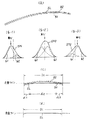
図中、符号S1、S2、S3、S4、S5は、副走査方向に連なる5本の「走査ライン」を示している。また、符号SL1、SL2、SL3、SL4、SL5は、単一の光スポットにより連続して行われた5回の光走査により「被走査面上に仮想的に記された走査線」を示している。即ち、光スポットによる光走査は、走査線SL1、SL2、SL3、SL4、SL5の順に行われる。
【0092】
前述の如く「走査線は直線であることが理想」であり、仮に、理想的に直線状の走査線を実現できれば「各走査線を走査ラインに合致させた光走査」を実現できるが、実際の光走査においては前述の如く「走査線曲がり」が発生する。
【0093】
請求項1記載の光記録装置においては「分割書込み方式による画像データの書込み」が行われる。以下、この分割書込み方式を説明する。
分割書込み方式では、図1の例で言えば「1つの光スポットが被走査面上を移動して光走査が行われるとき、光スポットの移動軌跡である走査線の部分に着目し、走査線の部分部分が最も近い走査ライン用の画像データの書込みを行う」書込み方式である。
【0094】
このために、分割書込み方式では、図1の如く、有効走査領域を複数の領域:Di(i=1,2,..)に分割する。図1の例では、有効走査領域は6つの領域D1〜D6に分割されている。この分割の仕方は、走査線曲がり特性、即ち、走査線の曲がり具合に応じて定まる。
【0095】
走査線SL3を例にとると、光走査の開始側(図の左方)から光走査が進行するに連れて、走査線SL3は、領域:D1においては走査ラインS5に最も近く、領域:D2では走査ラインS4に最も近く、領域:D3では走査ラインS3に最も近く、領域:D4では走査ラインS2に最も近く、領域:D5では走査ラインS3に最も近く、領域:D6では走査ラインS4に最も近い。
【0096】
従って、光スポットが走査線SL3に沿って書込みを行うとき、領域:D1では走査ラインS5、領域:D2では走査ラインS4、領域:D3では走査ラインS3、領域:D4では走査ラインS2、領域:D5では走査ラインS3、領域:D6では走査ラインS4の画像データの書込みを行うのである。
【0097】
即ち、走査ラインの番号をkとし、書込むべき領域:Diと、この領域:Diに対して書込みを行う走査線の番号:jとで、画像データを印付ける。k番目の走査ラインの領域:Diにj番目の走査線で書込まれる画像データをDkijとする。具体的な例として、上に説明した走査線SL3による光走査の場合を考える、走査線を指定する指標:jとしてj=3とする。また走査ラインの番号としてはS1〜S5に応じてk=1〜5とする。
【0098】
例えば上記の如く、光スポットが走査線SL3にそって光走査を行うとき、走査線SL3を描く光スポットの光強度は、領域:D1では画像データ:D513、領域:D2では画像データ:D423、領域:D3では画像データ:D333、領域:D4では画像データ:D243、領域:D5では画像データ:D353、領域:D6では画像データ:D463で強度変調されることになる。
【0099】
図1の下の図は、上記のようにして、走査ラインSL3に対応して「走査線曲がりを補正された光走査」で画像データを書込まれた1ライン分の書込み画像を示している。この書込み画像は、領域ごとに異なる走査線で書込まれている。
【0100】
即ち、走査ラインSL3を書込むための画像データは、領域:D1では画像データ:D311、領域:D2では画像データ:D322、領域:D3では画像データ:D333、領域:D4では画像データ:D344、領域:D5では画像データ:D353、領域:D6では画像データ:D362のように分割され、領域:D1は走査線SL1、領域:D2は走査線SL2、領域:D3は走査線SL3、領域:D4は走査線SL4、領域:D5は走査線SL3、領域:D6は走査線SL2で書込まれる。
【0101】
図1の下の「走査ラインSL3に応じた書込み画像(上記分割書込み方式で主走査方向に長い直線を書き込んだものである)」を見ると、その個々の領域において、画像は不連続で「ギクシャク」しているけれども、書込まれた画像の副走査方向の変動範囲は、走査ラインSL1を中心として、隣接する走査ラインSL2とSL4との間の1走査ライン分の幅(走査ラインの1間隔幅)に収まっており、走査線にそって一連に書き込んだ場合(この場合には、書込まれた画像が走査線曲がりに一致して曲がることになり、図の例では走査ラインの4間隔分にまたがる)に比して有効に補正軽減されていることがわかる。
【0102】
走査線の曲がりを、例えば、有効走査領域幅:290mmに対して最大で0.5mmとすると、図1の下図のように書込まれた書込み画像における領域ごとのギクシャクの大きさは、図の場合でせいぜい0.1mm強程度になるので、走査線曲がりが有効に軽減されることは明らかであり、この程度のスケールで考えれば、上記画像のギクシャクは然程問題とならない。
【0103】
上に説明したように「分割書き込み方式」では、有効走査領域が走査線曲がり特性に応じて複数の領域:Di(i=1,2,..)に分割され、各光走査ごとに、複数走査ラインにおける画像データのうちから、各領域:Diの光走査に適した画像データを選択することにより、走査線曲がりに拘わらず、各走査ラインの画像データが、走査線曲がりを補正して書込まれる。
【0104】
図2は、画像形成装置の実施の1形態を説明するための図である。
この画像形成装置は、図2(b)に示すように、タンデム式のカラー画像形成装置で、図示されないシート状記録媒体の搬送路(図の右から左に向う)に沿うて、被走査面の実体をなす4つの光導電性の感光体8A’、8A、8B、8B’が配列され、それぞれ個別に光走査されるようになっている。
【0105】
図2(a)、(b)に示すように、光走査装置は、光源から走査結像光学系に至る部分が、光偏向走査手段である回転多面鏡のポリゴンミラー4の軸方向に重ねられている。
【0106】
光源からポリゴンミラー4に至る部分を見ると、図2(a)に示すように、半導体レーザである光源1Aから放射された光束はカップリングレンズ2Aによりカップリングされて平行光束(若しくは弱い発散性または弱い集束性の光束)に変換され、ビーム整形用のアパーチュアAPを通過してビーム整形され、線像結像光学系であるシリンドリカルレンズ3Aを透過し、副走査方向に集光され、ポリゴンミラー4の偏向反射面近傍に主走査方向に長い線像として結像する。
【0107】
上の光学系に重なり合うように設けられた光源1A’(半導体レーザ)から放射された光束はカップリングレンズ2A’によりカップリングされて平行光束(若しくは弱い発散性または弱い集束性の光束)に変換され、ビーム整形用のアパーチュアAP’を通過してビーム整形され、線像結像光学系であるシリンドリカルレンズ3A’を透過し、副走査方向に集光され、ポリゴンミラー4の偏向反射面近傍に主走査方向に長い線像として結像する。このとき結像される線像は、光源1Aからの光束による線像に対し、ポリゴンミラー4の軸方向(副走査方向)に分離している。
【0108】
半導体レーザである光源1Bと1B’、カップリングレンズ2Bと2B’、アパーチュアBPとBP’、シリンドリカルレンズ3Bと3B’も、ポリゴンミラー4の軸方向である副走査方向に重なり合うように配置されている。
【0109】
半導体レーザである光源1B(1B’)から放射された光束は、カップリングレンズ2B(2B’)によりカップリングされて平行光束(若しくは弱い発散性または弱い集束性の光束)に変換され、ビーム整形用のアパーチュアBP(BP’)を通過してビーム整形され、線像結像光学系であるシリンドリカルレンズ3B(3B’)を透過し、副走査方向に集光され、ポリゴンミラー4の偏向反射面近傍に主走査方向に長い線像として結像する。光源1B、1B’が結像する線像も、副走査方向に互いに分離している。
【0110】
ポリゴンミラー4は、図2(b)に示すように、回転軸方向に広い偏向反射面を持ち、4光束を同時に偏向走査できるようになっている。
光源1Aからの光束は、ポリゴンミラー4により偏向されると、レンズ5Aを透過し、光路折り曲げ用のミラーMA1、MA2、MA3により反射され、レンズ6Aを透過して被走査面の実体を成す光導電性の感光体8Aに導光され、fθレンズを構成するレンズ5A、6Aの作用により感光体8A上に光スポットとして集光し、感光体8Aを光走査する。
【0111】
光源1A’からの光束はポリゴンミラー4により偏向されると、レンズ5A’を透過し、光路折り曲げ用のミラーMAにより反射され、レンズ6A’を透過して被走査面の実体を成す光導電性の感光体8A’に導光され、fθレンズを構成するレンズ5A’、6A’の作用により感光体8A’上に光スポットとして集光し、感光体8Aを光走査する。
【0112】
光源1Bからの光束は、ポリゴンミラー4により偏向されると、レンズ5Bを透過し、光路折り曲げ用のミラーMB1、MB2、MB3により反射され、レンズ6Bを透過して被走査面の実体を成す光導電性の感光体8Bに導光され、fθレンズを構成するレンズ5B、6Bの作用により感光体8B上に光スポットとして集光し、感光体8Bを光走査する。
【0113】
光源1B’からの光束はポリゴンミラー4により偏向されると、レンズ5B’を透過し、光路折り曲げ用のミラーMBにより反射され、レンズ6B’を透過して被走査面の実体を成す光導電性の感光体8B’に導光され、fθレンズを構成するレンズ5B’、6B’の作用により感光体8B’上に光スポットとして集光し、感光体8Aを光走査する。
【0114】
例えば、感光体8A’,8A、8B、8B’にそれぞれイエロー、マゼンタ、シアン、黒の各画像に対応する静電潜像を書込み形成し、これら各潜像を対応する色のトナーで可視化して、イエロートナー画像、マゼンタトナー画像、シアントナー画像、黒トナー画像とし、これら各色画像を図示されないシート状記録媒体上に位置合わせして重ね合せて転写し、定着すればカラー画像を形成できる。
【0115】
その際に、各光源1A、1B、1A’、1B’の発光強度を変調する画像データの印加を、図示されない制御手段(コンピュータ等)で制御して、上に図1で説明した方法により「分割書き込み方式」を実行すれば、各感光体8A、8A’、8B、8B’に書込まれる画像は、走査線曲がりの存在に拘わらず、走査線曲がりを有効に補正されたものとなるので、前述した走査線曲がりに起因する色ずれの問題を有効に軽減できる。
【0116】
即ち「図2に示す光走査装置に、図1の分割書込み方式を適用したもの」は、画像データに基づき変調された光源1A、1A’、1B、1B’からの光束を光偏向走査手段4により主走査方向に偏向し、偏向光束を走査結像光学系5A、6A、5A’、6A’、5B、6B、5B’、6B’により被走査面8A、8A’、8B、8B’に向けて集光し、被走査面上に光スポットを形成し、光スポットにより被走査面を光走査する光走査装置において、有効走査領域を、走査線曲がり特性に応じて複数の領域:Di(i=1,2,..)に分割し、各光走査ごとに、複数走査ラインにおける画像データのうちから、各領域:Diの光走査に適した画像データを選択することにより、走査線曲がりに拘わらず、各走査ラインの画像データを、走査線曲がりを補正して書込む分割書込み方式を実行する光走査装置(請求項1)である。
【0117】
請求項1記載の光走査装置で行われる分割書込み方式では、上に説明したように走査線曲がりは有効に補正されるけれども、この補正は図1下図の、走査ラインS3の書込み画像に示されたように、必ずしも「完全な」補正というわけではなく、更なる微調補正(微小な調整を行う補正)が望まれる。
【0118】
請求項2記載の説明では、このような微調補正が行われる。
請求項2記載の光走査装置で行われる微調補正を説明する。
この微調補正は「光源から複数の光束を放射させ、被走査面上に副走査方向に近接した2以上の光スポットを形成する。そして、複数の光束の光強度分布を副走査方向に重畳した合成光強度分布における重心位置を、各光束の強度を調整することにより可変とし、分割書込み方式で補正しきれない1走査ライン内の走査線曲がりを微調補正する(請求項2)」補正である。
【0119】
図3(a)において、符号B1、B2は「光源から放射された2光束が、被走査面上に形成する2つの光スポットの移動軌跡」を示している。2つのスポットの移動軌跡は「副走査方向に近接」している。
図3(b−2)は、被走査面上における2つの光スポットb1、b2の光強度分布を主走査方向から見た図であり、図の左右方向は副走査方向に相当する。図3(b−2)に示すように、光スポットb1、b2の光強度分布が互いに等しいと、両光スポットは副走査方向に近接しているので、これらの光強度分布は互いに合成されて実線で示すような合成光強度分布SPOを生じる。
【0120】
上の説明における「複数の光束の光強度分布を副走査方向に重畳した合成光強度分布における重心位置」とあるのは、図3(b−2)の場合に即して言えば、合成光強度分布SPOの(副走査方向における)最大強度位置である。
光走査が行われる間、光スポットb1、b2の光強度分布を「互いに等しく設定」しておけば、図3(a)において、2つの光スポットが移動軌跡B1、B2を描くとき、合成光強度分布SPOは図3(a)の実線の如き軌跡SLを描き、被走査面は実質的に合成光強度分布SPOにより走査されるので、被走査面における走査線は実線で示す「軌跡SL」に合致することになる。
【0121】
図3(b−1)は、光スポットb1、b2の発光強度をアンバランスにし、光スポットb2の光強度を、光スポットb1の光強度よりも小さくした場合であり、このとき合成光強度分布SP1の重心位置は図の如く「左方へずれ」る。同様に、図3(b−3)は、光スポットb1、b2の発光強度をアンバランスにし、光スポットb1の光強度を、光スポットb2の光強度よりも小さくした場合であり、このとき合成光強度分布SP1の重心位置は図の如く「右方へずれ」る。
【0122】
従って、もし、合成光強度分布SP1で光走査を行えば、被走査面における走査線SLは、図3(a)において軌跡B1の側に近づくことになるし、合成光強度分布SP2で光走査を行えば、被走査面における走査線SLは、図3(a)において軌跡B2の側に近づくことになる。
【0123】
即ち、2つの光スポットb1、b2の光強度分布の大小関係を調整すると、合成光強度分布における重心の位置(被走査面を光走査する「合成の光スポットの中心」の位置)を副走査方向にずらすことができる。
【0124】
そこで、例えば、前述した分割書込み方式による走査線曲がりの補正を行った結果、「ある走査領域:Di」における走査線SLの形状が、図3(c)に示す如きものであった場合に、領域:Di内の区間:di1では光スポットb2の光強度を大きく、区間:di2では光スポットb1の光強度を大きく、区間:di3では光スポットb2の光強度を大きくすることにより、合成光強度分布の重心を走査ラインに近づけると、その結果として、合成光強度分布の重心の軌跡である走査線SLを、図3(d)に示すように実質的に走査ラインに極めて良く合致させることができる。
【0125】
分割書込み方式において「分割された他の領域:Dj」においても同様にして走査線曲がりを走査ラインに「より合致」させることができ、このようにして、分割書込み方式で補正しきれなかった走査線曲がりを、さらに微調補正して良好な走査線を実現できる。
【0126】
若干付言すると、上の説明においては、光スポットb1、b2が副走査方向に並んでいるものとして説明を行ったが、実際には、これら光スポットb1、b2は、必ずしも副走査方向に完全に並んでいる必要はなく、相互に主走査方向にずれていても構わない。光スポットb1、b2で露光されるタイミングが多少ずれても、合成された露光分布に大きな影響は与えない。即ち、被走査面の実体をなす感光媒体の露光量は、光スポットb1、b2の光強度のスカラー和であり、これらが同時に露光を行う必要は無いのである。さらには、光スポットb1、b2を、同一の光束による連続した光走査により「時間的にずらして形成」することもできる。
【0127】
また、上には、2つの光スポットb1、b2を用いる場合を説明したが、3以上の光スポットの合成光強度分布で走査線を形成することも可能で、この場合には、各光スポット相互の光強度分布を調整することにより、より精細な微調補正を行うことができる。
【0128】
このように複数の光スポットの「合成光強度分布の重心移動」で走査線曲がりの微調補正を行う場合、各光スポットが互いに分離せず、副走査方向の解像度を劣化させないためには、各光スポットにおける光強度分布の最大強度の1/e2で定義される、被走査面上での副走査方向の静止光スポット径:Ws、隣接する光スポットによる走査軌跡間隔:Lが下式を満足することが好ましい。
【0129】
1.2<Ws/L<4.5
パラメータ:Ws/Lが下限値の1.2を下回ると、光スポット相互の重なり具合が少なくなり、合成光強度分布の形状が「一山形状」とならず、合成光強度分布による光走査が難しくなる。また上限を超えると、合成光強度分布の副走査方向の幅が小さくなるため、その重心移動の移動幅が小さく、有効な微調補正を行うことが難しい。
【0130】
なお、図2に示した画像形成装置において、上記請求項2記載の発明を実施するには、例えば、光源における発光源として、半導体レーザ発光部が2以上アレイ配列されたモノリシックな半導体レーザアレイを用い、各半導体レーザ発光部からの光束を被走査面上に複数の、副走査方向に近接した光スポットを形成し、各半導体レーザ発光部からの発光光束を強度変調するようにすればよい。
【0131】
分割書込み方式により補正された走査線曲がりをさらに微調補正する方法は、上記請求項2記載のもののほかにも、請求項3記載のものがある。
即ち、請求項3記載の光走査装置では、分割書込み方式で補正しきれない1走査ライン内の走査線曲がりを微調補正するのに「光源からの光束を副走査方向に偏向可能な偏向手段」を用い、偏向手段による光束の偏向により、被走査面上における光スポット位置を副走査方向に変位」させる。
【0132】
偏向手段としては「液晶偏向素子」を用いる(請求項4)ことも、「偏向ミラー」を用いることもできる(請求項5)が、先ずは液晶偏向素子を用いる場合を説明する。
【0133】
液晶偏向素子は、液晶を用いて光偏向を行う光学素子であり、従来から種々のものが知られている。液晶偏向素子は、電気的な信号で駆動されるものと、磁気的な信号で駆動されるものとが知られているが、ここでは電気的な信号で駆動されるものを例にとって説明する。
【0134】
電気的な信号による駆動で光束を偏向させる液晶偏向素子は、大別すると、電気信号により「屈折率を変化させる」ものと、電気信号により「回折作用を起こさせる」ものとの2種に分けられる。
【0135】
屈折率の変化を利用する液晶偏向素子は、例えば、前述の特許文献3に記載されている。これは、液晶に屈折率の勾配を形成することにより、透過光束を偏向させるものである。このような液晶偏向素子を駆動する電気信号としては「パルス状または正弦波状に変調された信号で、平均電圧が0V近傍であるもの」が好ましく、この場合、パルス信号の「パルスのデュ−ティ比」を変えることによって偏向量を制御することができる。
【0136】
図5に示すのは「電気信号で回折作用を起こさせるタイプの液晶偏向素子」の1例である。このタイプの液晶偏向素子は、例えば、前述の特許文献4に詳しく記載されている。
【0137】
図5において、液晶偏向素子17は液晶セル171とこれを駆動する駆動回路172で構成されている。液晶セル171は平行に対向させられた1対のガラス基板1711、1712の対向する面に、ITO等による透明電極1713、1714を形成し、これら透明電極に配向膜1715、1716を形成し、スペーサ1717、1718を介して配向膜1715、1716に挟まれた空間に、液晶170を薄層状に封入したものである。駆動回路172は、透明電極1713、1714間に駆動電圧を印加する。
【0138】
液晶170は例えば「液晶分子の分子軸方向の誘電率が、分子軸に直交する方向の誘電率よりも小さい、誘電異方性が負のネマチック液晶」で、配向膜1715、1716により、液晶分子の分子軸方向が図面に直交する方向となるように配向されている。
透明電極1713、1714間に駆動回路172により「直流もしくは300Hz程度以下の低周波の電圧」を印加すると、液晶171内に配向方向と直交する方向(図の上下方向)を格子配列方向とする回折格子パターンが形成される。
【0139】
この状態で、図の如く入射光束を液晶セル171に入射させると、透過光は上記回折格子パターンにより回折光を生じる。上記低周波の電圧の電圧値を変化させると、形成される回折格子パターンの格子ピッチが変化し、回折角が変化する(特許文献3「0057」)。
【0140】
従って、例えば「回折の1次光」に着目すれば、1次光の偏向角を調整することにより、光束を所定方向(上の場合では、図5の上下方向)に所望の偏向角で偏向させることができる。また、液晶セル171の透明電極1713、1714間に印加する電圧を高周波電圧にすると、液晶170に配向方向に直交する方向の回折格子パターンが現れ「図面に直交する方向の回折光」が得られる。この場合は、液晶に印加する高周波電圧の「包絡電圧」を増減させることにより、回折角を変化させることができる(特許文献4「0060」)。
【0141】
図4には、液晶偏向素子を利用して走査線曲がりの微調補正を行う実施の形態を2例示す。
図4(a)に示す光走査装置では、半導体レーザとカップリングレンズとにより構成される光源装置10から平行光束(もしくは弱い発散性または弱い集束性の光束)が射出し、液晶偏向素子17を透過し、シリンドリカルレンズ12により副走査方向に集光されてポリゴンミラー14の偏向反射面近傍に主走査方向に長い線像を結像する。
【0142】
ポリゴンミラー14により反射された偏向光束は、走査結像光学系としてのfθレンズ16を構成するレンズ161、162を透過し、被走査面20上に光スポットを形成し、光走査が行われる。このとき、図示されない制御手段の作用により「画像データの組換え」が行われ、被走査面に対する「分割書込み方式」による画像書込みが行われる。
【0143】
図4(a)に示す光走査装置は、偏向手段が液晶偏向素子17を有し、この液晶偏向素子17とコントローラ22が「偏向手段」を構成する。コントローラ22は画像形成装置全体を制御する前記制御手段(マイクロコンピュータ等)における機能の1つとして設定されている。
【0144】
液晶偏向素子17は、図5に即して説明した如きものであり、回折作用を利用して光束の偏向を行うが、これに限らず屈折率分布を形成して偏向を行うものでも良いし、磁気信号により駆動されるものであってもよい。
【0145】
光スポットによる光走査が行われるごとに、コントローラ22が液晶偏向素子17による「光束の副走査方向への偏向量」を制御し、前述した分割書込み方式で補正しきれない走査線曲がりの微調補正を行う。
【0146】
図4(b)に示す光走査装置では、偏向手段が液晶偏向素子アレイ18とコントローラ22とで構成されている。液晶偏向素子アレイ18は、図4(a)に示した液晶偏向素子17と同様の機能を持ったものを、主走査方向に複数個、長尺にアレイ配列したものであり、アレイを構成する各液晶偏向素子が、所定区間における微調補正を行う。図4(a)における液晶偏向素子17は「光スポットの光走査ごと」に光走査の時間内で微調補正のために偏向量を切り換え制御する必要があるが、図4(b)の液晶偏向素子アレイ18を用いると、光走査ごとの微調補正を一括して行えるため、応答速度が遅い液晶偏向素子を用い得るというメリットがある。
【0147】
上には偏向手段として、液晶偏向素子を用いる場合を説明した。走査線曲がりの微調補正を行うための偏向手段は、液晶偏向素子以外にも可能であり、請求項5記載の光走査装置のように「偏向ミラー」を用いることもできる。偏向ミラーは、反射面の向きを比較的小さい範囲で高速に変化させることのできる光学デバイスであり、種々のものが知られている。代表的な2例を、図6(a)、(b)に示す。
【0148】
図6(a)に示す「偏向ミラー」は、電磁力を駆動力とするものである。
基板61は、図示されない支持機構により、軸62の回りに揺動自在に支持されており、その一方の面にミラー面67が形成され、このミラー面67を囲繞するようにコイル65が形成され、振動素子となっている。この振動素子を図の上下から挟むように固定磁石63、64が固定的に設けられ、振動素子の上下方向に磁場を作用させている。基板61には、図示されないバネによる弾性力が作用され、この弾性力により中立位置を保つようになっている。
【0149】
コイル65に駆動回路66から駆動電流を通ずると、コイル65を流れる駆動電流に対して固定磁石63、64の作用する磁場の作用によるローレンツ力が、振動素子に回転モーメントを生じさせ、これによりミラー面67の向きが変化する。コイル65に通ずる電流は、矩形波あるいは正弦波または直流であることができる。直流電流を通じた場合には、ミラー面の向きを一定の向きに維持固定することができる。
【0150】
コイル65に通ずる電流の制御により、ミラー面67の向きを制御できる。基板61はシリコン等からなり、コイル65やミラー面67は蒸着やメッキなどの方法で薄膜形成される。このように、単一のシリコン基板61上にコイル65やミラー面67を形成することにより、半導体生成プロセスを使用でき軽量かつ安価に製作可能である。振動素子は軽量であるので、高速駆動を少ないエネルギで実現できる。
【0151】
図6(b)に示す「偏向ミラー」は、圧電効果を利用した例である。
固定板68は固定して設けられている。この固定板68に対し揺動基板69が軸72を共通として蝶番状に係合されて揺動自在と成っている。揺動基板69には蒸着やメッキ等の方法でミラー面70が薄膜形成されている(蒸着形成に替えて揺動基板をアルミ金属で構成し、その表面を鏡面加工しても良い。)。
【0152】
揺動基板69と固定板71の自由端部側で挟まれるように圧電素子71が固定されている。2KHz以上の高周波電気信号を発生する駆動回路73により圧電素子71を駆動して、揺動基板69を軸72の回りに回転させることができる。
【0153】
図6(a)、(b)に即して説明したような偏向ミラーを、光源と光偏向走査手段との間に配置し、光源側からの光束を副走査方向に偏向させることにより、前述の「分割書込み方式で補正し切れなかった走査線曲がり」の微調補正を行うことができる。
【0154】
図6(c)、(d)は、上記の如き偏向ミラー75をシリンドリカルレンズ12と光偏向走査手段との間に配置し、光源側からの光束を副走査方向に偏向させるようにした例を2例示している。例えば、図4(a)、(b)に示す実施の形態から、液晶偏向素子17、液晶偏向素子アレイ18を取り除き、光偏向走査手段の光源側を図6(c)あるいは(d)に示すように変更することにより、上記微調補正が実現されることは容易に理解されるであろう。
【0155】
なお、液晶偏向素子や偏向ミラーによる偏向手段を用いて「微調補正」を行うことは、図2に示した光走査装置においても実施可能であることは言うまでも無い。
【0156】
上に説明した請求項1〜5の発明では「副走査方向の走査位置の理想位置からのずれ」である走査線曲がり(走査線の傾きを含む)の補正を行った。走査特性としては上述のように、主走査方向の走査特性としての等速特性(fθ特性)に起因する光スポットの主走査方向の「走査位置のずれ」も存在する。「走査位置のずれ」は、主走査方向と副走査方向とで略独立であるから、副走査方向のずれの補正と、主走査方向のずれの補正は、同時に行うこともできる。
【0157】
即ち、請求項6記載の光走査装置では、上に説明した請求項1〜5の任意の1に記載の光走査装置において行われる走査線曲がりの補正に加え、光スポット位置を主走査方向に補正的に調整する。このために「書込む画像データの画素クロックよりも高い高周波クロックに基づき、画素クロックの位相シフトを行」う。「画素クロック」は、光スポットに1画素を書込ませるためのクロック信号である。
【0158】
fθ特性に起因する光スポットの「主走査方向の位置ずれ」を電気的に補正することは従来から知られている。fθ特性に起因する光スポットの主走査方向の位置ずれは、光スポットの主走査方向の移動速度が等速にならないことに起因するのであるから、基本的には、光スポットの移動速さが規定の速さ(理想上のfθ特性が実現される時の速さ)よりも大きい(あるいは小さい)ところでは、画素クロックの立ち上がりのタイミングを早く(あるいは遅く)し、同時に、画素クロックの時間幅を縮める(あるいは延ばす)ことにより、光スポットが当該画素を書込むドット位置を調整できる。
【0159】
このような調整を1画素単位で行えば、原理的には光スポットの主走査方向の位置ずれを完全に補正できる。
【0160】
図7に、光スポットの主走査方向の位置の調整を実施する場合の1例を示す。
【0161】
図7(a)に示すように、光走査装置の偏向光束が被走査面700上に形成する光スポットの有効走査領域の両側にフォトセンサ701、702を配し、光走査が行われるときに、フォトセンサ701、702間を光スポットが移動する時間を計時カウンタ703によりカウントし、カウント値をルックアップテーブル704に入力する。
【0162】
光走査装置におけるfθ特性(等速特性)は予め知られており、ルックアップテーブルには「計時カウンタによりカウントされた値に応じて、主走査方向の位置を補正する補正量」が記憶されており、この記憶内容に基づきカウント値に応じた補正量が設定される。
【0163】
補正値は位相同期回路705に印加される。位相同期回路705にはクロック生成回路706からクロックが入力される。クロック生成回路706で生成するクロックは「画素クロックに比して高周波」である。クロックの周波数が、画素クロックの周波数のn倍(例えば8倍)であるとすると、このようなクロックで画素クロックを生成させると、画素クロックの立上がりのタイミング(位相)を、画素クロックの基準長さ:Tに対し、T/n刻みでシフトさせることができ、また、画素クロックの長さもT/n刻みで変化させることができる。
【0164】
位相同期回路705は、クロック生成回路706から入力するクロックを用い、ルックアップテーブル704からの補正量に応じて「立上がりタイミングと信号長さをシフトされた画素クロック」を発生し、これを画像処理回路707に印加する。画像処理回路707は、画像データと画素クロックとを半導体レーザ駆動回路708に印加する。
【0165】
半導体レーザ駆動回路708は、画像データに応じて画素クロックに基づき、所定のタイミングで光源の半導体レーザ709を点滅させ、その点滅のタイミングと点灯時間とに応じて、主走査方向の位置を調整された光スポットによる画像データ書込みが行われる。
【0166】
例えば、等速特性に基づく「光スポットの主走査方向の位置ずれ」が、図7(b)上図の如くに変化するものとする。図7(b)において、上下方向は主走査方向の位置ずれ量を表し、横軸は光スポットの像高を表している。
【0167】
このような場合に、主走査方向の位置ずれの補正を行う1つの方法として、図7(b)上図のように、像高の範囲を8つの領域に分ける(この8分割は、説明と図示の簡単化のためであり、実際には15〜30分割程度が適当である。また、分割も等分割するよりは、光スポットの移動速度の大きい部分ほど細かく分割するように、不等間隔に分割するのがよい。)。
【0168】
そして、このように分割された領域ごとに「画素クロックの位相シフト量と信号長さを一律に」定め、各分割領域で、この領域に対して定められた位相シフト量と信号長さの画素クロックで光書込みを行うと、図7(b)下図のように、光スポットの像高ごとの主走査方向のずれは、補正前(図7(b)の上図)に比して有効に軽減される。像高の範囲を分割する分割数を大きくするほど、主走査方向のずれを良好に軽減できる。
【0169】
上に、走査線曲がり(走査線の傾きを含む)の調整と、主走査方向の位置調整とを説明した。このような補正を行うには、光走査装置を組み込んだ画像形成装置の「初期調整」の際に、上記補正内容を最適化すればよいが、実際上の画像形成装置で長期間にわたる運転が行われる場合には、補正対象が経時的に変化することも考えられるし、また、樹脂製の光学素子が用いられる場合には、温度・湿度といった環境条件の変化で光学特性が変化して、上記補正対象が変動する。
【0170】
このような観点からすると、走査線曲がりや主走査方向の走査位置ずれを適時に検出し、検出結果に応じて補正を最適化できることが好ましい。
【0171】
請求項7記載の光走査装置は、これを実現するために「偏向光束の光スポットの走査位置を検出する走査位置検出手段」を有する。
【0172】
図8(a)に示す走査位置検出手段80は、固定板81に設けられた複数のエリアセンサP1、P2、・・Pi、・・の受光面を主走査方向に配列させた構成となっている。走査位置検出手段80は、各エリアセンサPiの受光面が「被走査面と光学的に等価な位置」を占めるように配設され、偏向光束もしくは偏向光束の一部を分離した検出光束で走査されるようになっている。エリアセンサPiとしては、2次元CCD、CMOSセンサなどが用いられる。
【0173】
例えば、光走査による画像形成プロセスを行うに先立ち、光源を発光させ、光走査を行う。このとき、光源の発光は時間的に間欠的に行い、発光ごとに上記偏向光束もしくは検出光束が、走査位置検出手段80の各エリアセンサPiに順次に入射するようにする。
【0174】
走査位置検出手段80はエリアセンサPi(i=1、2、・・)が検出する光スポットの「副走査方向の位置」を演算手段(例えば、画像形成装置の全体を制御する制御手段の機能の一部として設定できる)に向けて出力する。
【0175】
図8(b)において「曲線Slにそって配列された1群の黒丸」が、このように検出された副走査方向の位置を示している。この図における破線は「走査ライン」で、主走査方向に直線的である。
【0176】
コントローラは、検出された「副走査方向の光スポット位置(走査位置)」に基づき、最小2乗法等により、走査線の形態を「多項式」として近似する。この多項式が「検出された走査線曲がり」であり、曲線Slがこれを示す。
【0177】
各エリアセンサPiにより主走査方向の走査位置を検出すれば、上記の如くしてfθ特性に起因する、光スポットの主走査方向の位置ずれを特定できる。
【0178】
ここで、走査位置検出手段80による走査位置の検出を説明する。
上に説明した例では、走査位置検出手段80はエリアセンサPiの受光面が被走査面と光学的に等価な位置を占めるように配設され、偏向光束もしくは偏向光束の一部を分離した検出光束で走査されるが、この場合の具体例を図9(a)、(b)に示す。
【0179】
図9(a)で、図面に直交する方向が主走査方向、上下方向が副走査方向である。因みに、図4(b)に示す光走査装置における走査位置検出は、図9(a)に示す如き方式で行われ、液晶偏向素子アレイ18は、主走査方向に偏向される結像光束の光路上において「副走査方向に対して若干傾け」て配設されている。
【0180】
このため、結像光束はその一部が液晶偏向素子アレイ18の入射側面で反射されて検出光束LSとなり、上記入射側の面を反射面として被走査面20と等価な面に配置された走査位置検出手段80の受光面位置に光スポットを形成し、走査位置を検出される。
【0181】
図9(b)でも、図面に直交する方向が主走査方向、上下方向が副走査方向である。主走査方向に偏向され、液晶偏向素子アレイ18を透過した結像光束は、結像光束光路上において「副走査方向に対して傾け」て配設された反射面部材19により反射され、反射面部材19の反射面に関して被走査面20と等価な面に配置された走査位置検出手段23の受光面位置に光スポットを形成し、走査位置を検出される。
【0182】
反射面部材19は、これを透明ガラスで構成して常時図示の位置に設置し、結像光束の一部を反射により走査位置検出手段80側へ分離するようにしても良いし、結像光束の光路に出入可能とし、走査位置検出を行うときにのみ図示の位置に設置するようにしてもよい。
【0183】
図9(a)、(b)に示したのは、偏向光束による光スポットを直接検出して、走査位置の検出を行う場合であるが、走査位置検出は、必ずしも光スポットの検出により行う必要はない。走査位置検出の別例を図9(c)、(d)に示す。
【0184】
図9(c)において、符号25は「被走査面の実体」をなす光導電性の感光体を示している。走査位置は感光体25の感光面に対する光スポット位置であるから、画像形成プロセスにより走査線1ライン分を感光体25に書込み、得られる静電潜像を可視化して線状のトナー画像LTIを得ると、このトナー画像LTIは走査線を可視化したものとなっている。
【0185】
トナー画像LTIをランプ26で照射し、結像系27によりイメージセンサ28上に結像させて読取り、その結果に基づき走査線曲がりを検出できる。この場合、ランプ26、結像系27、イメージセンサ28が「走査位置検出手段」を構成する。
【0186】
図9(d)において、符号29は、中間転写媒体としての中間転写ベルトを示している。図9(c)の場合と同様にして感光体25上に形成した線状のトナー画像LTIを、転写手段30により中間転写ベルト29上に転写し、転写されたトナー画像LTIをランプ26で照射し、結像系27によりイメージセンサ28上に結像させて読取り、その結果に基づき走査線曲がりを検出する。この場合も、ランプ26、結像系27、イメージセンサ28が「走査位置検出手段」を構成する。
【0187】
図9(c)、(d)の場合とも、線状のトナー画像LTIは、検出後、図示されないクリーニング手段により感光体25、中間転写ベルト29から除去される。
【0188】
等速特性の検出のために、主走査方向の走査位置検出を行うには、「副走査方向に適宜の長さとなる直線状の画像」を互いに平行となるようにして主走査方向に必要な本数だけ書込み、これを可視化する。
【0189】
各「副走査方向の直線」の間隔は、等間隔を理想とするように形成する。これら直線を可視化したものを、感光体上もしくは中間転写ベルト上で検出し、各直線間の間隔を調べることにより等速特性を知ることができる。
【0190】
以上は走査位置検出手段により走査位置を検出する場合であるが、走査位置検出手段を持たない場合には以下の如くにすれば良い。即ち、この場合には、上記の如くして形成したトナー画像を転写紙上に転写・定着し、転写紙上に得られた画像に基づき走査線曲がり(走査線の傾きを含む)、等速特性を測定し、その結果に基づき、液晶偏向素子アレイの各液晶偏向素子における偏向量を決定する。
【0191】
勿論、光学系が環境変動の影響を受けない場合や、環境変動の影響を自動的に補正するように構成されている場合には、予め測定により走査線曲がりや等速特性を測定し、そのデータによる補正用データを制御手段に記憶させておいて、上記の如き補正を行えば良い。
【0192】
図10は請求項8記載の発明を説明するための図であり、図1に倣って描いてある。図1におけると同じく、符号S1〜S5は「相続く5本の走査ライン」を示している。図1との相違は以下の点にある。即ち、図1においては符号SL1〜SL5は、単一の光スポットが相次ぐ光走査により描く走査線であったが、図10において符号SL1〜SL4は、4つの光スポットにより同時に走査される走査線である。即ち、図10の実施の形態においては、被走査面は、4つの光スポットにより線順次方式でマルチビーム走査される。各走査線SL1〜SL4は実質的に同一の走査線曲がり特性を有している。
【0193】
即ち、請求項8記載の光走査装置は、画像データに基づき変調された光源からの光束を光偏向走査手段により主走査方向に偏向し、偏向光束を走査結像光学系により被走査面に向けて集光し、被走査面上に光スポットを形成し、光スポットにより被走査面を光走査する光走査装置において、光源から複数の光束を放射させ、これら複数の光束が被走査面上で副走査方向に分離した複数の光スポットを形成し、且つ、各光スポットの走査線曲がり特性が実質的に同一となるようにして、これら複数の光スポットにより被走査面を同時に光走査するようにする。
【0194】
複数の光スポットは副走査方向の間隔が、略走査ライン間隔と一致するように設定し、光学系の像高間の倍率を略等しくすれば、走査線曲がりは各々ほぼ同等と見なして良い。
【0195】
そして、有効走査領域は、走査線曲がり特性に応じて複数の領域:Di(図の例ではi=1〜4)に分割され、複数光スポットによる同時の光走査ごとに、走査ラインごとに複数の光束のうちから「各領域:Diの光走査に適した光束」が選択され、走査線曲がりに拘わらず、各走査ラインの画像データを、走査線曲がりを補正して書込む「光束選択書込み方式」が実行される。
【0196】
例えば、図10における走査ラインS4への画像書込みを例にとると、この走査ラインS4への書込みに際しては、領域:D1では走査線SL2の走査に与る光束を選択し、領域:D2では走査線SL3の走査に与る光束を選択し、領域:D3では走査線SL4の走査に与る光束を選択し、領域:D4では走査線SL3の走査に与る光束を選択して画像書込みを行うのである。
【0197】
他の走査ラインS1、S2等でも同様に「光束選択書込み方式」が並行して行われ、一度の光走査で4本の走査ラインを同時に画像書込みすることができる。このようにして、マルチビーム走査方式の持つ光走査の高速性を活かしつつ、走査線曲がりを有効に補正して良好な光走査を実現できる。
【0198】
勿論、この請求項8記載の発明においても、前述した各種の微調補正が適用でき、主走査方向の走査位置の調整を併用できることは言うまでも無い。
【0199】
図11は、画像形成装置の実施の別形態を示している。
この画像形成装置は、光導電性の感光体を感光媒体とし、カラー画像を形成するためのものである。形成されるべきカラー画像は、イエロー、マゼンタ、シアン、黒の4色の成分画像を形成し、これら成分画像を同一のシート状記録媒体上で重ね合せることにより得られる。
【0200】
符号151、152はポリゴンミラーを示す。ポリゴンミラー151、152は同一形状のもので共通の軸に固定的に設けられ、一体として回転するようになっており、図示されない駆動手段と共に「光偏向走査手段」を構成する。
【0201】
図示されていないが「4つの光源装置」が設けられている。4つの光源装置のうち2つからの光束はポリゴンミラー151に入射し、他の2つからの光束はポリゴンミラー152に入射する。各光源装置からポリゴンミラー151、152に至る光路上の光学配置は、図2の画像形成装置のものと同様である。
【0202】
ポリゴンミラー152により偏向される偏向光束LSY、LSKはそれぞれ、イエロー成分画像、黒成分画像を書込むための光束である。
偏向光束LSYはイエロー色成分の画像情報で強度変調され、走査結像光学系としてのfθレンズを構成するレンズLNY1、LNY2(保持体PTYに保持されている)を透過し、光路折曲げミラーMY1、MY2、MY3により順次反射され、光導電性の感光体150Yの感光面(被走査面の実体を成す)に導光され、上記感光面を光走査する。
【0203】
感光体150Yは円筒状で、矢印方向へ回転しつつ帯電器CYにより均一帯電された状態で、偏向光束LSYの光スポットで光走査され、イエロー成分画像を書込まれてイエロー潜像を形成される。
【0204】
偏向光束LSKは黒色成分の画像情報で強度変調され、fθレンズを構成するレンズLNK1、LNK2(保持体PTKに保持されている)を透過し、光路折曲げミラーMK1、MK2、MK3により順次反射され、光導電性の感光体150Kの感光面に導光され、上記感光面を光走査する。
【0205】
感光体150Kは円筒状で、矢印方向へ回転しつつ帯電器CKにより均一帯電された状態で、偏向光束LSKの光スポットで光走査され、黒成分画像を書込まれて黒潜像を形成される。
【0206】
ポリゴンミラー151により偏向される偏向光束LSM、LSCはそれぞれ、マゼンタ成分画像、シアン成分画像を書込むための光束である。
偏向光束LSMはマゼンタ色成分の画像情報で強度変調され、fθレンズを構成するレンズLNM1、LNM2(保持体PTMに保持されている)を透過し、光路折曲げミラーMM1、MM2、MM3により順次反射され、光導電性の感光体150Mの感光面に導光され、上記感光面を光走査する。
【0207】
感光体150Mは円筒状で、矢印方向へ回転しつつ帯電器CMにより均一帯電された状態で、偏向光束LSMの光スポットで光走査され、マゼンタ成分画像を書き込まれてマゼンタ潜像を形成される。
【0208】
偏向光束LSCはシアン色成分の画像情報で強度変調され、fθレンズを構成するレンズLNC1、LNC2(保持体PTCに保持されている)を透過し、光路折曲げミラーMC1、MC2、MC3により順次反射され光導電性の感光体150Cの感光面に導光され、上記感光面を光走査する。
【0209】
感光体150Cは円筒状で、矢印方向へ回転しつつ帯電器CCにより均一帯電された状態で、偏向光束LSCの光スポットで光走査され、シアン成分画像を書込まれてシアン潜像を形成される。
【0210】
各感光体の光走査は、説明中の例では「シングルビーム走査方式」で行うが、「マルチビーム走査方式」で行ってもよい。シングルビーム方式で光走査を行う場合には上述の「分割書込み方式」が実行され、マルチビーム走査方式で光走査を行うときは、図10に即して説明した「光束選択書込み方式」が実行される。また、必要に応じ、請求項6記載の発明による「光スポットの主走査方向の位置調整」や前述の各種「微調補正」が行われる。
【0211】
これら分割書込み方式や光束選択書込み方式に必要な画像データの組替え制御は、図示されない制御手段(マイクロコンピュータ等で構成され、画像形成装置全体を制御する)で行われる。
【0212】
また、各感光体を帯電する帯電器としてコロナ放電式のものを例示したが、帯電ローラや帯電ブラシ等の接触式のものを用いても良い。
【0213】
感光体150Y、150M、150C、150Kに形成されたイエロー、マゼンタ、シアン、黒の各潜像は、それぞれ対応する現像装置153Y、153M、153C、153Kにより、対応する色のトナー(イエロートナー、マゼンタトナー、シアントナー、黒トナー)により現像されて可視化される。
【0214】
このようにして、感光体150Yにはイエロートナー画像、感光体150Mにはマゼンタトナー画像、感光体150Cにはシアントナー画像、感光体150Kには黒トナー画像がそれぞれ形成される。これら各トナー画像は、以下のようにしてシート状記録媒体である転写紙P上に転写される。
【0215】
感光体150Y、150M、150C、150Kに、図の下方から接するように無端状の搬送ベルト154がプーリ155、156に掛け回されて設けられており、搬送ベルト154の内周面側において、転写器157Y、157M、157C、157K(コロナ放電式のものを例示したが、転写ローラ等の接触式のものを用いることもできる)が、ベルト面を介して対応する感光体150Y〜150Kに対向するように設けられている。
【0216】
シート状記録媒体としての転写紙Pは積載収納されているカセット158内から給紙され、送り込みローラ159により搬送ベルト154上に乗せ掛けられ、帯電器160による帯電を受けて搬送ベルト154の外周面に静電吸着されて保持される。搬送ベルト154は反時計回りに回転し、転写紙Pを周面に保持して搬送する。
【0217】
転写紙Pは上記の如く搬送されつつ、先ず、感光体150Y上のイエロートナー画像を転写器157Yにより転写され、続いて、感光体150M、150C、150K上の、マゼンタ、シアン、黒の各色トナー画像を順次、転写器157M、157C、157Kにより転写される。各色トナー画像の転写は、これらトナー画像が互いに位置合わせされて重なり合うように行われる。
【0218】
このようにして転写紙P上にカラー画像が形成される。カラー画像を形成された転写紙Pは、除電器161により除電され、自身の腰の強さにより搬送ベルト154から剥離し、定着装置162によりカラー画像を定着され、排出ローラ163により、画像形成装置の天板を兼ねたトレイ164上に排出される。
【0219】
トナー画像を転写された後の各感光体は、対応するクリーナ165Y、165M、165C、165Kにより残留トナーや紙粉等を除去される。また、搬送ベルト154は除電器166により除電され、クリーナ167によりクリーニングされる。
【0220】
以上が「フルカラーモードにおける画像形成プロセスのあらまし」である。感光体150Kに対してのみ画像形成を実行することにより、モノクロームの黒白画像を形成できるし、画像形成を行う感光体の組合せにより2色画像や多色画像の形成も可能になる。
図11に示した実施の形態における各色トナー画像の転写紙への転写方式に代えて周知の「中間転写ベルトに各色トナー画像を転写してカラー画像とし、このカラー画像を転写紙に転写する転写方式」を行うようにしてもよい。
【0221】
前述の如く、このカラー画像形成装置において、走査結像光学系はfθレンズであり各偏向光束ごとに1組ずつ、全部で4組が設けられ、各組は2枚のレンズで構成されている。これら4組のfθレンズは「互いに光学的に等価」で、各光源装置から対応する感光体に至る光路長も互いに等しく設定されている。これらは光学ハウジング175内に設けられている。
【0222】
レンズLNY1、LNM1、LNC1、LNK1は同一の樹脂材料で構成され、レンズLNY2、LNM2、LNC2、LNK2も同一の樹脂材料で構成されている。これらレンズの材料樹脂としては、低吸水性や高透明性、成形性に優れたポリカーボネートやポリカーボネートを主成分とする合成樹脂が好適である。樹脂材料で構成すると非球面の形成も容易であるし、材料費も安いため、カラー画像形成装置の低コスト化上有利である。
【0223】
反面、樹脂レンズは温・湿度変化の影響で光学特性が変化するので、走査線曲がり・走査線の傾きや等速特性も環境変化に応じて変動する。そこで、図4(b)に即して説明した液晶偏向素子アレイ18と同様の液晶偏向素子アレイ170Y、170M、170C、170Kを、各感光体150Y、150M、150C、150Kを光走査する偏向光束の光路上に図の如く設け、先に説明した如くして、各感光体上における光スポットの位置を副走査方向に調整し、また画像クロックの位相シフトにより主走査方向に調整することにより走査線曲がり・等速特性を補正する。
【0224】
図11に示すようなタンデム式のカラー画像形成装置では、各感光体上に形成される画像における走査線曲がりが、感光体相互で互いに異なると「色ずれ」の問題が顕著に現れるので、上記のようにして走査線曲がりを各感光体ごとに補正して、これらが実質的に同じになるようにすることにより「色ずれ」の問題を有効に軽減若しくは防止することができる。
【0225】
なお、図11に図示していないが、各偏向光束LSY〜LSKが対応感光体上に形成する光スポットの走査位置はそれぞれ、図8(b)に即して説明した走査位置検出手段80(各被走査面と光学的に等価な位置に配置される)と同様のものにより検出され、偏向光束の一部を走査位置検出手段に導くため、液晶偏向素子アレイ170Y〜170Kは(図では明らかでないが)、図9(a)に即して説明したように、各偏向光束の光路上で副走査方向に対して若干傾けて配置され、検出光束を各走査位置検出手段(図示されず)に向けて反射する。
【0226】
上記のように、全ての走査結像光学系を樹脂レンズで構成するのではなく、そのうちの1組、例えばレンズLNK1、LNK2の組を「走査位置基準となる光学系」として、温度変動による影響をなくすため「熱膨張率の小さ」いガラスで構成し、偏向光束LSY、LSM、LSCの光路内に設けた液晶偏向素子アレイ170Y、170M、170Cにより、偏向光束LSY、LSM、LSCによる光走査における走査線曲がりや光スポットの主走査方向の位置調整を「レンズLNK1、LNK2により結像される偏向光束LSKの走査線曲がりや主走査方向の走査位置に合わせる」ように補正を行うことができる(請求項9)。
【0227】
この場合、レンズLNK1、LNK2によるfθレンズは、他のfθレンズと光学特性を等価にし、他のfθレンズの光路内に液晶偏向素子アレイを用いることによる光路長の差を補正するために、液晶偏向素子アレイ170Kに代えて、これと光学的厚さ(物理的な厚さに屈折率を掛けたもの)が等価な透明平行平板を用いる。
【0228】
このようにすると、液晶偏向素子アレイを全ての偏向光束の光路上に搭載する必要が無く、また高価なガラスレンズは基準となる走査結像光学系のみに使用され、他の走査結像光学系は安価なプラスチックレンズを使用できるので、全体として安価なカラー画像形成装置を実現でき、色ずれの少ない高品質のカラー画像を得ることが可能になる。
【0229】
即ち、このようなカラー画像形成装置は、光導電性の感光体をN(=4)個、シート状記録媒体Pの搬送路に沿って配置し、各感光体に別個の静電潜像を光走査により書込み形成し、各静電潜像を色の異なるトナー画像として可視化し、これらトナー画像を同一のシート状記録媒体上に重ね合せて転写・定着するタンデム式の画像形成装置において、感光体ごとに光走査装置を有し、感光体のうちのひとつ(感光体150K)には黒トナー画像が形成され、この黒トナー画像が形成される感光体以外のN−1(=3)個の感光体150Y、150M、150Cに対する光走査装置は上に説明した請求項1〜8の任意の1に記載のものを用いることができ、黒トナー画像を基準として、走査線曲がり・光スポット位置の主走査方向の補正のうち、少なくとも、走査線曲がりの補正を行うものである(請求項9)。
【0230】
この請求項9記載の画像形成装置のように、黒トナー画像を基準として、他の色の画像における走査線曲がり等を補正するが、カラー画像における画像品質のうち、解像度(鮮鋭性)、粒状性(ざらつき)に支配的な影響を与えるのは、黒トナー画像である。黒トナー画像を基準として、他の色のトナー画像の走査線曲がり等を補正することにより、色ずれと共に、解像度、粒状性を同時に満足する高画質カラー画像を得ることができるとともに、補正が必用とされるデータ量が少なく済むため、コスト的に有利となる。
【0231】
なお、この発明における走査線曲がり補正は、従来の機構的な走査線曲がり補正と組合せても有効であることは言うまでもない。
【0232】
以下には、先に説明した参考例の光走査装置の実施形態を説明する。光走査装置の形態としては図2に示す如きものを想定する。したがって、光走査装置の構成・動作については、図2に即した前述の説明を援用する。
【0233】
図2を参照すると、参考例の光走査装置は、変調駆動される光源1A(1A'、1B、1B')からの光束を光偏向走査手段4により偏向させ、偏向光束を、走査結像光学系5A、6A(5A'、6A'、5B、6B、5B'、6B')により導光して被走査面8A(8A'、8B、8B')上に光スポットを形成し、光スポットにより被走査面を光走査する光走査手段を複数(4手段)用い、複数の被走査領域8A、8A'、8B、8B'を光走査し、所望の画像を合成するべき画像を複数の被走査領域に分けて書込む光走査装置である。
【0234】
即ち、この光走査装置においては、光源の個々(1A、1A’、1B、1B’)からの光束を、対応する被走査面(8A、8A’、8B、8B’)に導光して光スポットを形成する各光学素子の組合せ(例えば、光源1A、カップリングレンズ2A、アパーチュア1P、シリンドリカルレンズ3A、光偏向走査手段4、レンズ5A、6A、光路折り曲げ用のミラーMA1〜MA3)がそれぞれ光走査手段を構成し、光導電性の感光体8A、8A’、8B、8B’の感光面が個々の被走査面であって且つ「被走査領域」である。即ち、被走査領域は4つで、副走査方向へ配列されている。
【0235】
前述の説明のように、感光体8A’,8A、8B、8B’にそれぞれイエロー、マゼンタ、シアン、黒の各画像に対応する静電潜像を書込み形成し、これら各潜像を対応する色のトナーで可視化して、イエロートナー画像、マゼンタトナー画像、シアントナー画像、黒トナー画像とし、これら各色画像を不図示のシート状記録媒体上に位置合わせして重ね合せて転写し、定着してカラー画像を形成するものとする。
【0236】
このとき、少なくとも1つの被走査領域において、副走査方向に隣接する走査線間に重心を有する露光分布を形成し、重心の副走査方向の位置を可変とするのであるが、この実施の形態においては、「黒以外の色のトナーにより可視化される静電潜像」を形成される被走査領域である感光体8A'、8A、8Bに対する画像書込みを行うに際して「副走査方向に隣接する走査線間に重心を有する露光分布」を形成する。
【0237】
この実施の形態において、感光体8A’〜8B’の個々に対する光走査は「シングルビーム走査方式」で行われ、「副走査方向に隣接する走査線間に重心を有する露光分布」は、相次ぐ光走査により形成される。
【0238】
また、黒トナーにより可視化さるべき静電潜像を形成される感光体(被走査領域)における走査線(「黒走査線」という。)を基準とし、他の感光体8A’、8A、8Bにおける走査線(それぞれ「イエロー走査線」、「マゼンタ走査線」、「シアン走査線」という。)を相対的に補正し、各色トナー画像を重ね合せるとき、イエロー、マゼンタ、シアンの各走査線が黒走査線と重なり合うようにする場合を説明する。
【0239】
黒走査線は一般に走査線曲がりを生じているが、ここでは説明の簡単のために、黒走査線が直線であり、他の色の走査線を直線的に補正するものとする。
【0240】
イエロー・マゼンタ・シアン走査線の補正は何れも原理的には同じであるから、イエロー走査線の補正を説明する。
【0241】
図12を参照すると、図12(a)において符号SL1、SL2はそれぞれ、感光体8A’の光走査による走査線を示している。図の上下方向が副走査方向である。上述の如く、光走査はシングルビーム走査方式で行われるので、ある光走査により走査線SL1が形成され、これに続く光走査により走査線SL2が形成される。
【0242】
走査線に書込まれる画像を「主走査方向に長い線」とすると、走査線SL1上に光スポットSP1が密接して照射されて長い線状の潜像が形成される。また走査線SL2は光スポットSP2により露光される。
【0243】
図12(a)は、走査線SL1、SL2に「走査線曲がり」の無い理想的な状態(走査線と走査ラインが合致している状態)を示している。走査線SL1は光スポットSP1の中心部(光スポットはガウス型の光強度分布を有し、この強度分布の最大強度部の位置に相当する)を連ねた線となり、図においては直線である。同様に、走査線SL2は光スポットSP2の中心部を連ねた直線となる。
【0244】
実際の走査線には一般に「走査線曲がり」が存在する。図12(b)は「走査線曲がりがある場合」を説明図的に示している。走査線SL1、SL2は上述の場合と同様、相続く2回の光走査により光スポットが走査する軌跡である。このように走査線SL1に走査線曲がりが存在する場合、これを補正して直線状の走査線SL0を得るには、走査線SL1を光走査するときの光スポットSP1と、走査線SL2を走査するときの光スポットSP2との光強度分布を合成した露光分布を利用する。
【0245】
例えば、図12(b)における位置:Aを考えてみると、補正の目的となる直線化された走査線SL0は、走査線SL1とSL2との間にあって、やや走査線SL1よりの位置を通っている。
【0246】
そこで、図12(c)に示すように、光スポットSP1により走査線SL1の光走査を行うとき、位置:Aにおいては、(c−1)の如く、光スポットSP1の光強度分布として「やや強め」の光強度分布SP1(A)で露光を行う。続いて走査線SL2の光走査を行うとき、位置:Aにおいては、(c−2)に示すように、やや弱めの光強度分布SP2(A)を光スポットに付与する。なお、図12(c)において、横軸は副走査方向、縦軸は露光強度を表す。
【0247】
このようにすると、図12(c)の(c−3)に示すように、走査線SL1、SL2が光走査される際に、位置:Aにおいては、光強度分布SP1(A)とSP2(A)との和として露光分布SPAが形成されることになり、このとき、露光分布SP(A)の重心位置が位置:Aにおける走査線SL0の位置を与えることになる。即ち、(c−3)で、位置:Aにおける走査線SL1と露光分布SP(A)の重心との距離:DAが、図12(b)に示す位置:Aにおける走査線SP1と走査線SL0との差に等しくなる。
【0248】
なお、露光分布の重心位置変位のために、各光スポットの光強度分布を調整する方法としては、「各画素を書込む変調時間を変える(パルス幅変調)」や「光源から放射される光束の光量を変える(パワー変調)」、さらにはこれらを組合せる方法が可能である。
【0249】
図12(b)における位置:Bでは、走査線の補正の目的である走査線SL0は走査線SL1、SL2の略中間にあるので、このときは図12(d)に示すように、走査線SL1の光走査の際、位置:Bにおける光スポットの光強度分布を図中の光強度分布SP1(B)のようにし、走査線SL2の光走査の際、位置:Bにおける光スポットの光強度分布を光強度分布SP1(B)に略等しい光強度分布SP2(B)のようにし、これらの合成による露光分布SP(B)の重心位置が、走査線SL1、SL2の略中央となるようにする。
【0250】
このとき、走査線SL1と上記重心との距離:DBは、図12(b)に示すように位置:Bにおける走査線SL1とSL0との距離になる。
【0251】
同様に、図12(b)における位置:Cでは、走査線の補正の目的である走査線SL0は走査線SL1、SL2の間で「走査線SL1よりの位置」にあるので、このときは図12(e)に示すように、走査線SL1の光走査の際、位置:Cにおける光スポットの光強度分布を図中の光強度分布SP1(C)のように大きくし、走査線SL2の光走査の際、位置:Bにおける光スポットの光強度分布を弱い光強度分布SP2(C)のようにし、これらの合成による露光分布SP(C)の重心位置が「走査線SL1よりの位置」となるようにする。
【0252】
このとき、走査線SL1と上記重心との距離:DCは、図12(b)に示すように位置:Cにおける走査線SL1とSL0との距離になる。
【0253】
光走査の全域にわたって、上記の如く、走査線SL1を光走査するときの光スポットSP1の光強度分布と、走査線SL2を光走査するときの光スポットの光強度分布を相対的に制御し、これら光スポットにより形成される露光分布の重心位置が、走査線SL0に沿って推移するようにして、走査線曲がりを直線的に補正した走査線SL0を得ることができる。
【0254】
即ち、副走査方向に隣接する走査線SL1、SL2の間に露光分布を形成する被走査領域(感光体8A')において、主走査方向に長い1ドットラインを形成するとき、隣接する走査線SL1の一方から、副走査方向における露光分布の重心までの距離を、主走査方向の位置に応じて異ならせることができる。そして、隣接する走査線SL1の一方から、副走査方向における露光分布の重心までの距離を、主走査方向の位置に応じて連続的に変化させることができる。
【0255】
上の説明から明らかなように、露光分布の重心の位置は、露光分布を形成することになる2つの光スポット(相次ぐ光走査により形成される)の光強度分布の相対的な大小関係を調整することにより、上記2つの光スポット間において任意に変位させることができるから、露光分布の重心位置を、直線化することは勿論、所望の曲線に合わせることもでき、露光分布の重心位置の軌跡(補正された走査線)の位置を副走査方向へ変位させることもできる。
【0256】
このようにして、イエロー走査線の走査線曲がりや副走査方向の位置を調整して、黒走査線に合致させ、イエロートナー画像が黒トナー画像と良好に重なりあうようにできる。
【0257】
例えば、図13に示すように、黒走査線SLBLに対してイエロー走査線SLY1が傾いているような場合、イエロー走査線SLY1を光走査する光スポットとイエロー走査線SLY2を光走査する光スポットの形成する露光分布の重心位置SLYが黒走査線SLBLと合致するようにできる。即ち、この場合、イエロー走査線SLY1を光走査するときの光スポットは、その強度を図の左側から右側へ光走査位置が変化するにしたがって次第に強くし、イエロー走査線SLY2を光走査するときの光スポットは逆に当初は強く、次第に弱くなるように光強度を調整される。
【0258】
上に説明した例は、走査線SL1、SL2を補正して、これら走査線SL1、SL2の間に露光分布の重心により「補正された走査線」を形成する場合であるが、走査線の曲がりがある程度大きいと、このような補正では、補正された走査線を直線にできない場合もある。このような場合には、走査線の補正に、3以上の走査線を光走査する光スポットを関与させることにより、所望の補正を実行できる。図14はこのような場合の例である。
【0259】
走査線SL1〜SL3が、相次ぐ3回の光走査における光スポットの軌跡である。走査線の曲がりを補正して直線状の走査線SL0を得る場合を考えて見ると、例えば、位置:Aでは、走査線SL0の位置は走査線SL3の位置に合致しているから、位置:Aにおいては、図14(b)の如く、走査線SL3を光走査する際の光スポットの光強度分布SP3(A)で露光を行う。
【0260】
位置:Bでは、走査線SL2を光走査する際の光強度分布SP2(B)(同図(c)参照)で露光を行い、位置:Cでは、同図(d)に示すように、走査線SL1を光走査するときの光スポットの光強度分布SP1(C)と、走査線SL2を光走査するときの光スポットの光強度分布SP2(C)との露光分布の重心位置が走査線SL0の位置に合致するようにし、位置:Dでは、同図(e)に示すように、走査線SL1を光走査するときの光スポットの光強度分布SP1(D)で露光を行う。
【0261】
このように、3本の走査線SL1、SL2、SL1の光走査にかかわる光スポットの1個もしくは2個の組合せにより、直線状の走査線SL0を実現できる。勿論、4本以上の走査線の光走査にかかわる光スポットの1個もしくは2個を組合せて補正を行うことができることは言うまでも無い。
【0262】
このようにすると、主走査方向に長い1ドットラインを形成するための露光分布の重心位置は、副走査方向に隣接する2つ以上の走査線(図14(a)で走査線SL1とSL2)をまたがって変位可能である。
【0263】
上にはイエロー走査線を補正(副走査方向の位置補正や走査線曲がり補正)して、黒走査線に合致させる場合を説明したが、上記と全く同様にして、マゼンタ走査線やシアン走査線を補正して、黒走査線と合致させることができる。
【0264】
即ち、複数の被走査領域(感光体8A'、8A、8B、8B')を副走査方向に設定し、被走査領域の少なくとも1つ(感光体8A'、8A、8B)において、副走査方向に隣接する走査線間に重心を有する露光分布を形成し、重心の副走査方向の位置を変位させることにより、複数の被走査領域相互における副走査方向の相対的な光走査位置を補正することができ、複数の被走査領域相互における相対的な走査線の曲がりを補正することができる。
【0265】
上記複数の被走査領域相互における副走査方向の光走査位置の補正は「走査線相互の曲がりが補正された段階で、各走査線の副走査方向における相対的な位置を調整する」ことであり、これは「露光分布の形成の仕方」でも実現できるが、前述したように「少なくとも1つの光走査手段において、光源の変調駆動タイミングの調整により、走査線位置を副走査方向に調整可能」とすることにより、調整がさらに容易となる。
【0266】
上に説明した実施の形態は、図2に即して説明した光走査装置の実施の形態であったが、上記走査線の補正は勿論、図11の画像形成装置においても実施することができる。このように、図11の画像形成装置の上記走査線補正を適用したものは、複数の被走査領域をそれぞれ光導電性の感光体150Y〜150Kとし、これらに光走査により静電潜像を形成し、これら静電潜像を異なる色のトナーで可視化し、各色トナー画像を同一のシート状記録媒体P上に重ね合せて転写して画像形成を行う画像形成装置において、複数の被走査領域を光走査する光走査装置として、参考例の光走査装置を用いたものである。
【0267】
また、複数の被走査領域に形成された静電潜像を可視化するトナーのうちの1種は黒色トナーであり、副走査方向に隣接する走査線間に重心を有する露光分布を形成することにより形成される静電潜像が、黒以外の色のトナーにより可視化される。
【0268】
図15は、請求項10以下に記載された光走査装置の実施の1形態を示す図である。この実施の形態では、被走査面の実体をなす光導電性の感光体48が、その主走査方向(回転軸方向)に2つの被走査領域A、Bに分割されている。即ち、複数の被走査領域A、Bが主走査方向に配列されている。これら被走査領域A、Bは光走査手段A、Bによりそれぞれ光走査される。
【0269】
光走査手段A(B)は変調駆動される光源41A(41B)からの光束を光偏向走査手段45A(45B)により偏向させ、偏向光束を走査結像光学系46A(46B)により導光して被走査面48上に光スポットを形成し、光スポットにより被走査面48の複数の被走査領域A(B)を光走査し、所望の画像を合成するべき画像を複数の被走査領域A(B)に分けて書込む光走査装置を構成する。
【0270】
各光走査手段において、符号42A、42Bは光源(半導体レーザ等)からの光束をカップリングするカップリングレンズ、符号43A、43Bはビーム整形用のアパーチュア、符号44A、44Bはシリンドリカルレンズ、符号47A、47Bは光路折曲げ用ミラー、符号49A、49Bは光センサを示している。
【0271】
光走査手段A(B)において、光源42A(42B)からの光束はカップリングレンズ42A(42B)によりカップリングされ、アパーチュア43A(43B)によりビーム整形され、シリンドリカルレンズ44A(44B)によりポリゴンミラー45A(45B)の偏向反射面位置に主走査方向に長い線像として結像され、ポリゴンミラー45A(45B)による偏向光束は、走査結像光学系46A(46B)の作用により、被走査領域A(B)上に光スポットとして集光される。
【0272】
走査結像光学46A、46Bを透過した光束の光路は、光路折り曲げ用ミラー47A、47Bで光路を折り曲げられ、各光束は光センサ49A、49Bにより検出され、その検出結果に基づき「光走査の同期」が取られる。
【0273】
被走査領域A、Bのうち少なくとも1つの被走査領域において「副走査方向に隣接する走査線間に重心を有する露光分布」を形成し、重心の副走査方向の位置を可変とすることができる。
【0274】
例えば、光走査手段Aが「被走査領域Aにおいて、副走査方向に隣接する走査線間に重心を有する露光分布を形成し、重心の副走査方向の位置を可変とする」機能を持つものとすると、図16(a)に示すように、被走査領域Aの走査線SL1、SL2等が、被走査領域Bにおいて対応する走査線SLBと副走査方向に食い違っている場合に、走査線SLA1、SLA2間に露光分布を形成し、その重心の軌跡による走査線SLA0が走査線SLBと繋がるようにできる。
【0275】
即ち、被走査領域の少なくとも1つである被走査領域Aにおいて、副走査方向に隣接する走査線SLA1、SLA2間に重心を有する露光分布を形成し、重心の副走査方向の位置を変位させることにより、複数の被走査領域A、B相互における副走査方向の相対的な光走査位置を補正することができる。
【0276】
勿論、主走査方向に設定された複数の被走査領域A、Bにおいて、副走査方向に隣接する走査線間に重心を有する露光分布を形成し、重心の副走査方向の位置を変位させることにより、複数の被走査領域相互における相対的な走査線の曲がりを補正することができる。このことは、先に、図12〜図14に即して説明したところから明かであろう。
【0277】
図15の如き光走査装置においても、少なくとも1つの光走査手段(例えば、光走査手段A)において、光源の変調駆動タイミングの調整により、走査線位置を副走査方向に調整可能であるようにし、この変調駆動タイミングの調整による走査線位置の調整と、露光分布の重心位置の変化による補正とを組み合わせることにより「より容易」に補正を行うことができる。
【0278】
あるいはまた、図16(b)に示すように、光走査領域Aにおける走査線SLA1、SLA2等と、被走査領域Bにおける走査線SLB1、SLB2等が「互いに異なる傾き方」をしているような場合に、光走査領域A、Bにおいて、露光分布を形成する補正により、被走査領域A、Bに滑らかに繋がる走査線SLA0、SLB0を形成できる。
【0279】
被走査面の実体をなす光導電性の感光体48に形成される静電線像をトナー画像として可視化し、さらに同一のシート上記録媒体に転写するように構成した画像形成装置は「複数の被走査領域A、Bをそれぞれ光導電性の感光体とし、これらに光走査により静電潜像を形成し、これら静電潜像をトナーで可視化し、同一のシート状記録媒体上に合成的に転写して画像形成を行う画像形成装置」であって、複数の被走査領域A、Bを光走査する光走査装置として請求項10〜15の任意の1に記載の光走査装置を用いたもの(請求項16)である。
【0280】
図15に示す実施の形態においては、2個の光走査手段A、Bで2つの被走査領域A、Bを光走査したが、被走査領域・光走査手段の個数を3以上として良いことは言うまでも無い。このように主走査方向に複数の被走査領域を設定し、各被走査領域を個別の光走査手段で光走査するようにすると、たとえば、被走査面の主走査方向の長さを大きくすることにより、大きなサイズの画像を形成することが可能になる。
【0281】
また、光走査手段の個数を増やし、個々の被走査領域の「主走査方向の長さ」を短くすると、個々の被走査領域を光走査する光走査手段の画角を小さくすることができ、光走査手段の光学性能を高性能化しやすく、良好な画像形成が可能になる。
【0282】
被走査面を主走査方向に複数分割し、各被走査領域に別個の光走査を行って1画像を「被走査領域ごとの画像の合成により形成」する場合、走査線曲がりや走査線の傾きは「個々の被走査領域に形成される画像」では目立たなくても、被走査領域相互で図16(a)のような「走査線の食い違い」や、図16(b)のような「走査線の傾きの不連続」があると、合成的に得られた画像では際立って目立ち、画質を著しく劣化させるが、上記の如くして走査線の副走査方向の位置や、傾き、曲がりを補正することにより良好な画像を得ることができる。
【0283】
なお、図16に示す状態を1単位とし、これと同様のものを4単位、副走査方向に配列し、各感光体に形成される静電潜像を異なる色のトナーで可視化し、同一のシート状記録媒体に転写・定着して大サイズのカラー画像を得るようにできることは言うまでも無い。
【0284】
上に説明した実施の形態では被走査領域が複数あり、これらが主走査方向に配列されている場合であるが、上に説明した走査線の補正は、被走査領域が単一である場合にも適用できることは明らかである。即ち、図15の実施の形態において「光走査手段Aと被走査領域Aの部分を独立させたもの」は、従来から知られている光走査装置を構成している。
【0285】
このような光走査装置において上記の如き走査線補正を行うようにしたものは「変調駆動される光源からの光束を光偏向走査手段により偏向させ、偏向光束を走査結像光学系により導光して被走査面上に光スポットを形成し、光スポットにより被走査面を光走査する光走査手段を用い、被走査領域を光走査し、所望の画像を被走査領域に書込む光走査装置において、被走査領域において、副走査方向に隣接する走査線間に重心を有する露光分布を形成し、重心の副走査方向の位置を可変とする光走査装置」である。
【0286】
そしてこの光走査装置において、被走査領域に、主走査方向に長い1ドットラインを形成するとき、隣接する走査線の一方から、副走査方向における露光分布の重心までの距離を、主走査方向の位置に応じて異ならせることができ、隣接する走査線の一方から、副走査方向における露光分布の重心までの距離を、主走査方向の位置に応じて連続的に変化させることができ、主走査方向に長い1ドットラインを形成するための露光分布の重心位置が、副走査方向に隣接する2つ以上の走査線をまたがって変位可能であることができる。
【0287】
そして、被走査領域を光導電性の感光体とし、この感光体に光走査により静電潜像を形成し、この静電潜像をトナーで可視化し、シート状記録媒体上に転写して画像形成を行う画像形成装置において、被走査領域を光走査する光走査装置として、上に説明した光走査装置を用いた画像形成装置を構成することができる。
【0288】
なお、請求項10〜16に記載された各発明において、先に説明したfθ特性等の等速性の補正を併用できることは言うまでもない。
【0289】
【発明の効果】
以上に説明したように、この発明によれば新規な光走査装置・画像形成装置を実現できる。この発明の光走査装置は、走査線曲がりの補正や主走査方向の走査位置調整を簡易且つ容易に行うことができ、良好な光走査を実現できる。そして、このような光走査装置を用いるこの発明の画像形成装置は、良好な画像形成を行うことができる。とくに請求項10以下の発明にかかる光走査装置は、露光量分布の形成により走査線曲がり等を容易且つ確実に補正することができ、このような光走査装置によりタンデム式のカラー画像形成装置を構成するときは、色むらや色ずれのない良好なカラー画像を得ることができ、また、請求項10〜15の光走査装置では、大サイズの画像、あるいは高品質の画像を良好に書込むことができ、請求項16記載の画像形成装置は大サイズもしくは高品質の画像を得ることができる。
【図面の簡単な説明】
【図1】分割書込み方式を説明するための図である。
【図2】画像形成装置の実施の1形態を説明するための図である。
【図3】走査線曲がりの微調補正の1例を説明するための図である。
【図4】光走査装置の実施の形態を2例示す図である。
【図5】走査線曲がりの微調補正に用いる液晶偏向素子を説明するための図である。
【図6】偏向ミラーと、これを用いる微調補正を説明するための図である。
【図7】請求項6記載の発明による主走査方向の走査位置の補正を説明するための図である。
【図8】走査位置検出手段の実施の1形態を説明するための図である。
【図9】走査位置検出手段による走査位置検出を説明するための図である。
【図10】光束選択書込み方式を説明するための図である。
【図11】画像形成装置の実施の別形態を説明するための図である。
【図12】参考例の光走査装置における走査線曲がり等の補正を説明するための図である。
【図13】参考例の光走査装置における走査線の傾きの補正を説明するための図である。
【図14】参考例を説明するための図である。
【図15】請求項10記載の発明の実施の1形態を説明するための図である。
【図16】図15の実施の形態における走査線補正を説明するための図である。
【符号の説明】
S1〜S5 走査ライン
SL1〜SL5 走査線[0001]
TECHNICAL FIELD OF THE INVENTION
The present invention relates to an optical scanning device and an image forming device.
[0002]
[Prior art]
A light beam from a light source modulated based on image data is deflected in the main scanning direction by an “optical deflection scanning unit” such as a rotary polygon mirror, and the deflected light beam is scanned by a “scanning optical system” such as an fθ lens. An optical scanning device that forms a light spot on a surface to be scanned and optically scans the surface to be scanned with the light spot is related to an image forming apparatus such as an optical printer, an optical plotter, or a digital copying machine. And widely known.
[0003]
In an image forming apparatus using an optical scanning device, an “image forming process including an image writing step of writing an image by optical scanning” is generally performed, and the quality of an image to be formed depends on the quality of optical scanning. . The quality of the optical scanning depends on the “scanning characteristics in the main scanning direction and the sub-scanning direction” of the optical scanning device.
[0004]
The scanning characteristics in the main scanning direction include, for example, constant speed characteristics of optical scanning.
For example, when a rotary polygon mirror is used as the light deflection scanning means, the light beam is deflected at a constant angular velocity. Therefore, in order to realize the constant speed characteristic of the optical scanning, a scanning imaging optical system having an fθ characteristic is used. Used. However, it is not easy to realize perfect fθ characteristics due to the relationship with other performances required for the scanning imaging optical system. For this reason, in actual optical scanning, optical scanning is not performed completely at a constant speed, and the constant speed characteristic as a scanning characteristic is accompanied by “a deviation from ideal constant speed scanning”.
[0005]
The scanning characteristics in the main scanning direction are not limited to the case where the fθ characteristics are not sufficiently corrected, and the accuracy of the optical components of the optical scanning optical system and the mounting accuracy to the housing are deteriorated. This is also caused by fluctuations in the characteristics of optical components due to environmental fluctuations, and fluctuations in the direction of the rotation axis of the photosensitive member and the intermediate transfer member that form the actual surface to be scanned.
[0006]
The scanning characteristics in the sub-scanning direction include “scanning line bending” and “scanning line inclination”. Ideally, the scanning line is a “trajectory of the light spot on the surface to be scanned” and is a straight line. The optical scanning device is designed so that the scanning line is a straight line. It is common that the scanning line is bent due to an error or assembling error. Such a bending of the scanning line is called “scanning line bending”, and the degree of the bending is called “scanning line bending characteristics”.
[0007]
When using an "imaging mirror" as the scanning imaging optical system and providing an angle in the sub-scanning direction between the incident direction and the reflection direction of the deflected light beam on the imaging mirror, the scanning line should be used in principle. Even when bending occurs and the scanning image forming optical system is configured as a lens system, scanning line bending is inevitable in the multi-beam scanning method in which the scanned surface is "optically scanned with a plurality of light spots separated in the sub-scanning direction". It is a target.
[0008]
The “inclination of a scanning line” is a phenomenon in which a scanning line is not correctly orthogonal to a sub-scanning direction, and is a type of scanning line bending. Therefore, in the following description, “scanning line inclination” is included in the scanning line bending unless otherwise specified.
[0009]
If the constant speed characteristics of the optical scanning are not perfect, the formed image will be distorted in the main scanning direction, and the bending of the scanning line will cause the formed image to be distorted in the sub-scanning direction. In the case where an image is monochrome and written and formed by a single optical scanning device, the image is formed if scanning line bending and imperfections in constant velocity characteristics (deviation from ideal constant velocity scanning) are suppressed to some extent. Although "distortion that can be seen visually" does not occur in the resulting image, the distortion of such an image is still small.
[0010]
Even in the case of monochrome images, when the linearity in the image is emphasized in the output of CAD (computer-aided design) or the like, even a slight scan line curve can significantly degrade the quality of the output image. Becomes a problem that cannot be ignored.
[0011]
Conventionally, forming a three-color image of magenta, cyan, and yellow or a four-color image obtained by adding black as a color component image and forming a color image synthetically by superimposing these color component images is a conventional technique. From a color copier.
[0012]
In order to form such a color image, there is an image forming method called a “tandem type” in which component images of each color are formed on different photoconductors by different optical scanning devices. In the case of such an image forming method, If the scanning lines are different in the degree and inclination of the scanning lines between the optical scanning devices, even if the scanning line bending for each optical scanning device is corrected within a tentative allowable range, the slightest scan line Due to the mismatch, an image abnormality called “color shift” appears in the formed color image, and the image quality of the color image deteriorates.
[0013]
Further, as one of the appearances of the color misregistration phenomenon, there is a phenomenon that a color image does not have a desired color tone.
In recent years, with the aim of improving scanning characteristics, it has become common to employ a special surface represented by an aspheric surface in the imaging optical system of an optical scanning device, and such a special surface can be easily formed. “Imaging optical system made of resin material” which is possible and inexpensive is often used.
[0014]
The imaging optical system made of a resin material is susceptible to changes in the shape and refractive index of the element under the influence of changes in temperature and humidity, and optical characteristics are likely to change. Condition and constant velocity characteristics ". Then, for example, when forming several tens of color images continuously, the temperature inside the apparatus increases due to the continuous operation of the image forming apparatus, the optical characteristics of the imaging optical system change, and the The degree of bending and constant velocity characteristics of the scanning line to be written gradually change, and the color shift phenomenon may cause the color image to be completely different between the color image obtained at the beginning and the color image obtained at the end. is there.
[0015]
Japanese Patent Application Laid-Open Publication No. HEI 11-163873 describes forming an "exposure distribution in a sub-scanning direction on a surface to be scanned or a region to be scanned" performed in the second and tenth aspects of the invention. Japanese Patent Application Laid-Open No. H11-163,086 describes the point of “adjusting the scanning line position in the sub-scanning direction by adjusting the modulation drive timing of the light source”.
[0016]
Further, techniques related to the liquid crystal deflecting element used in the invention described in
[0017]
[Patent Document 1]
JP 2001-215437 A
[Patent Document 2]
JP 2000-235290 A
[Patent Document 3]
JP-A-8-313941 (0057)
[Patent Document 4]
JP-A-8-313941 (0060)
[0018]
[Problems to be solved by the invention]
SUMMARY OF THE INVENTION It is an object of the present invention to effectively correct a scan line bending in an optical scanning device, thereby enabling good optical scanning.
According to the present invention, in the optical scanning device, in addition to the correction of the bending of the scanning line, a better optical scanning can be performed by satisfactorily correcting the “deviation of the scanning position in the main scanning direction” caused by the constant velocity characteristic. The task is to make it possible.
[0019]
Still another object of the present invention is to make it possible to form a good image by optical scanning by using the optical scanning device in an image forming apparatus.
[0020]
It is still another object of the present invention to correct a relative shift, bend, or inclination of a scanning line between scanning regions when performing optical scanning of a plurality of scanning regions individually.
[0021]
[Means for Solving the Problems]
The optical scanning device according to
[0022]
“Image data” is a “set of data in pixel units” of an image to be formed by optical scanning, and the luminous flux emitted from the light source is intensity-modulated according to this image data, and the position of the scanned surface corresponding to the pixel is adjusted. Write to. The image data may be "a document to be copied and converted into data for each pixel", or may be generated by a computer, a word processor, a digital camera, an information terminal device, or the like. In some cases, the data is transferred as external data.
[0023]
The "light deflection scanning means" is a means for deflecting a light beam from the light source side in the main scanning direction for optical scanning. The light deflection scanning means includes a rotating polygon mirror for rotating a polygon mirror, a pyramidal mirror, a tenon type mirror or the like. Various conventionally known mirrors such as a plane mirror, a rotating two-sided mirror, and a galvanometer mirror can be used.
[0024]
The “scanning optical system” is an optical system for forming a light spot on the scanned surface by condensing the light beam deflected by the light deflection scanning unit toward the scanned surface, such as an fθ lens. It may be configured as a “lens system”, as an “imaging mirror system” such as an fθ mirror, or as a “combined system of a lens system and a mirror system”.
[0025]
The scanning imaging optical system can include a “resin imaging element”. In this case, the resin imaging element may constitute a part of the scanning imaging optical system, or the entire scanning imaging optical system may be comprised of the resin imaging element. Of course, a single resin imaging element may constitute the “scanning optical system itself”.
[0026]
The scanning image forming optical system has a “constant speed function” for equalizing the speed of light scanning by the light spot. For example, when the light deflection scanning unit deflects a light beam at a constant angular velocity, a scanning image forming optical system that has an fθ function to make scanning with a light spot at a constant speed is used. In this case, the “fθ characteristic” is the “optical scanning constant velocity characteristic”.
[0027]
The “scanned surface” is a surface that is optically scanned by a light spot, and is generally a photosensitive medium as a substance.
[0028]
Various types of "photosensitive medium" are possible. For example, a “silver salt film” can be used as a photosensitive medium. In this case, a latent image is formed by writing by optical scanning, and this latent image can be visualized by processing using a normal silver halide photographic process. An image forming apparatus using such a photosensitive medium can be implemented as an "optical plate making apparatus" or an "optical drawing apparatus" for drawing a CT scan image or the like.
[0029]
As the photosensitive medium, a "coloring medium that develops color by the thermal energy of a light spot during optical scanning" can be used. In this case, a visible image can be directly formed by optical scanning.
[0030]
As the photosensitive medium, a "photoconductive photoreceptor" can be used. The photoconductive photoreceptor may be in the form of a sheet such as zinc oxide paper, or may be a "repeatedly used in a drum or belt shape" such as a selenium photoreceptor or an organic optical semiconductor.
[0031]
The optical scanning device according to the first aspect has the following features.
That is, “the effective scanning area is divided into a plurality of areas: Di (i = 1, 2,...) In accordance with the scanning line bending characteristics, and for each optical scan, each of the image data in the plurality of scanning lines is selected. By selecting image data suitable for the optical scanning of the area: Di, a divisional writing method is executed in which the image data of each scanning line is written after correcting the scanning line curvature regardless of the scanning line curvature. "
[0032]
The “effective scanning area” refers to an area in the main scanning direction on the scanned surface on which the light spot optically scans, in which image data can be effectively written.
A “scan line” is a straight line obtained by idealizing a line constituting one line of an image on an image, and a series of image data constituting an image on this line is written in one scan line.
[0033]
In the optical scanning apparatus according to the first aspect, every time the light spot optically scans the surface to be scanned once, the image data of the plurality of scanning lines is selected, so that “the plurality of scanning lines are respectively partially written. Is included. " Therefore, the image data of one entire scanning line is written by a plurality of light scans using the light spot.
[0034]
Thus, in the optical scanning device according to the first aspect, in one optical scan by the light spot, the image data of a plurality of scan lines is divided and written, and the image data forming one scan line is written. This is performed by dividing the light spot into a plurality of times of light scanning, and such an optical scanning method is referred to as a “division writing method”.
[0035]
The light source of the optical scanning device according to
[0036]
The optical scanning device according to the first aspect may further include “deflecting means capable of deflecting the light beam from the light source in the sub-scanning direction”. It can be configured to be variable in the sub-scanning direction so as to finely correct a scan line curve in one scan line that cannot be corrected by the divided writing method.
[0037]
The "deflecting means" in the optical scanning device according to the third aspect may include one or more liquid crystal deflecting elements (claim 4) or may include "a deflecting mirror capable of adjusting the direction of the reflection surface". (Claim 5).
[0038]
The optical scanning device according to any one of
[0039]
"Adjusting the light spot position in the main scanning direction in a corrective manner" means that the position of the light spot on the surface to be scanned is matched or approximated to the "ideal position in the main scanning direction" for each image height. Means to adjust.
[0040]
The optical scanning device according to any one of the first to sixth aspects can include “scanning position detecting means for detecting the scanning position of the light spot of the deflected light beam”.
[0041]
The optical scanning device according to claim 8 has the following features.
That is, a plurality of light beams are emitted from the light source, and the plurality of light beams form a plurality of light spots separated in the sub-scanning direction on the surface to be scanned, and the scanning line bending characteristics of each light spot are substantially the same. In such a manner, the surface to be scanned is simultaneously optically scanned by the plurality of light spots.
[0042]
Further, the effective scanning area is divided into a plurality of areas: Di (i = 1, 2,...) According to the scanning line bending characteristics. Then, by selecting a light beam suitable for the light scanning of each region: Di from among the plurality of light beams for each scanning line for each “simultaneous light scanning by a plurality of light spots”, regardless of the scanning line bending. Then, the "light beam selective writing method for writing the image data of each scanning line by correcting the scanning line bending" is executed.
[0043]
That is, the luminous flux selective writing method is a multi-beam version of the above-described divisional writing method. Since there is one light spot in the divisional writing method, the scanning line for writing information is changed in accordance with the formation of a curved scanning line by this light spot. In the case where light scanning is performed simultaneously with a plurality of light spots whose surfaces are separated in the sub-scanning direction, the number of light spots can be set to N, and writing can be simultaneously performed on N scanning lines. When the division writing method is performed, each scanning line is selected from among a plurality of light beams that is most suitable for writing the scanning line (referred to as a “light beam selective writing method” due to this feature) and once. , N lines can be written.
[0044]
According to the image forming apparatus of the present invention, “N (≧ 2) photoconductive photoconductors are arranged along the conveyance path of a sheet-shaped recording medium, and a separate electrostatic latent image is written on each photoconductor by optical scanning. Tandem-type image forming apparatus that forms, visualizes each electrostatic latent image as a toner image having a different color, and superimposes and transfers and fixes these toner images on the same sheet-shaped recording medium. It has the following features.
[0045]
That is, each photoconductor has an optical scanning device, and a black toner image is formed on one of the photoconductors. The optical scanning device for the N-1 photoconductors other than the photoconductor on which the black toner image is formed is the one according to any one of
[0046]
The plurality of optical scanning devices may be independent and separate from each other. However, as described in an embodiment to be described later, "on the optical path from the light source to the surface to be scanned, some optical elements (for example, light deflection scanning means) Can be standardized. "
[0047]
The “photoconductive photoreceptor” is “a photoreceptor that is repeatedly used in a drum shape or a belt shape” such as a selenium photoreceptor or an organic optical semiconductor. The electrostatic latent image is formed by uniform charging of the photoconductor and optical scanning by an optical scanning device.
[0048]
The “sheet-shaped recording medium” on which the toner image is transferred and fixed is a transfer sheet, an OHP sheet (a plastic sheet for an overhead projector), or the like.
[0049]
The transfer of the toner image from the photoconductive photoconductor to the sheet-shaped recording medium may be directly performed from the photoconductor to the sheet-shaped recording medium (direct transfer method), or may be performed once from the photoconductor to an intermediate transfer belt or the like. After the image is transferred to the intermediate transfer medium, the image may be transferred from the intermediate transfer medium to a sheet-shaped recording medium (intermediate transfer method).
Such an image forming apparatus can be implemented as an optical color printer, an optical color plotter, a digital color copying machine, a color facsimile machine, or the like.
[0050]
This is described below as a reference exampleThe image forming apparatus uses an “optical scanning device that optically scans a plurality of scanned areas using a plurality of optical scanning units and writes an image to be combined with a desired image into the plurality of scanned areas”. The plurality of optical scanning units may be independent and separate from each other. However, as described in an embodiment described later, “on the optical path from the light source to the surface to be scanned, some optical elements (for example, optical deflection scanning units) Can be standardized. "
[0051]
The “light scanning means” deflects a light beam from a light source that is modulated and driven by the light deflection scanning means, guides the deflected light beam by the scanning and imaging optical system, and forms a light spot on the surface to be scanned. This is a means for optically scanning the surface to be scanned with a spot.Reference exampleThe image forming apparatus uses a plurality of such optical scanning units, and each optical scanning unit optically scans “different scanning target areas”.
[0052]
The “light flux from the light source that is modulated and driven” has the same meaning as the “light flux modulated based on the image data” described above. The “scanned area” is substantially a photosensitive surface of a photosensitive medium and includes the concept of the above-described scanned surface. However, separate scanned areas are “each photoconductive photoconductor”.
[0053]
In the image forming apparatus of the reference example,"In at least one scanned region, an exposure distribution having a center of gravity between scanning lines adjacent in the sub-scanning direction is formed, and the position of the center of gravity in the sub-scanning direction is made variable."
[0054]
“Exposure distribution having a center of gravity between scanning lines adjacent in the sub-scanning direction” is defined as “a case where two light spots adjacent to each other in the sub-scanning direction are formed on a scanning line adjacent to the scanning direction in the sub-scanning direction. In which the barycentric position in the combined light intensity distribution obtained by superimposing the light intensity distributions of these two light spots in the sub-scanning direction is between the adjacent scanning lines. The position of the center of gravity can be varied in the sub-scanning direction by relatively changing the light intensity of the two light spots, increasing one light intensity and decreasing the other light intensity.
[0055]
In the optical scanning device according to the second aspect, by adjusting the position of the center of gravity of the light intensity distribution formed in this way, "fine adjustment of the scanning line bending in one scanning line that cannot be completely corrected by the divided writing method" is performed. But,Reference exampleIn the optical image forming apparatus, the position of the center of gravity is adjusted over the entire length of the scanning line formed in the scanned area.
[0056]
Reference exampleIn the image forming apparatus, when “one dot line that is long in the main scanning direction is formed in a scanned area where an exposure distribution is formed between scanning lines adjacent in the sub-scanning direction”, the sub-scanning is performed from one of the adjacent scanning lines. The distance to the center of gravity of the exposure distribution in the direction can be "different according to the position in the main scanning direction"Can thisIn this case, according to the position of one dot line long in the main scanning direction in the main scanning direction, “the distance from one of the adjacent scanning lines to the center of gravity of the exposure distribution in the sub-scanning direction is continuously determined according to the position in the main scanning direction. Can be changed "Wear.
[0057]
The center of gravity of the exposure distribution isAccording to the position in the main scanning direction, it may be changed with a step in the sub scanning direction. That is, in this case, the position of the center of gravity of the exposure distribution is displaced stepwise in the sub-scanning direction.
[0058]
Reference example image forming apparatusIn that the position of the center of gravity of the exposure distribution for forming one long dot line in the main scanning direction can be displaced across two or more adjacent scanning lines in the sub-scanning direction.it can.
[0059]
Here, that the position of the center of gravity of the exposure distribution is “displaceable across two or more scanning lines adjacent in the sub-scanning direction” has the following meaning.
[0060]
That is, when scanning lines adjacent in the sub-scanning direction are scanning lines i-1, i, i + 1, the center of gravity of the exposure distribution formed by the light spot on the scanning line i-1 and the light spot on the scanning line i. Can be displaced between the scanning lines i-1 and i by adjusting the relative light intensity of these light spots. Further, the center of gravity of the exposure distribution of the light spot formed on each of the scanning lines i and i + 1 Can be displaced between scanning lines i and i + 1 by adjusting the relative light intensity of these light spots.
[0061]
In this way, by adjusting the light intensity of two adjacent light spots among the light spots formed on three or more scanning lines while writing one scanning line, the center of gravity of the exposure distribution becomes “ It can be displaced between two or more scanning lines (in the above example, scanning lines i-1, i, and i + 1). Such a case is referred to as “the center of gravity of the exposure distribution is displaced across two or more scanning lines”.
[0062]
Optical scanning device used in the image forming apparatus of the above reference example, "A plurality of scanned areas can be set in the sub-scanning direction". In at least one of the plurality of scanned areas set in this way, "a center of gravity exists between adjacent scanning lines in the sub-scanning direction. By forming an “exposure distribution” and displacing the position of the center of gravity in the sub-scanning direction, it is possible to correct the relative optical scanning position in the sub-scanning direction among a plurality of scanned regions.it can.Of course, in this case as well, the "center of gravity of the exposure distribution is displaced across two or more scanning lines".
[0063]
Reference example aboveIn the image forming apparatus, "a plurality of scanned regions are set in the sub-scanning direction, and in at least one of the scanned regions, an exposure distribution having a center of gravity between scanning lines adjacent to each other in the sub-scanning direction is formed. By displacing the position in the sub-scanning direction, it is possible to correct the relative scanning line bending among a plurality of scanned areas. "it can.The “bending of the scanning line” includes the inclination of the scanning line.
[0064]
Setting the plurality of scanned areas in the sub-scanning direction in this way can be realized, for example, by setting each of the scanned areas to be a photoconductive photoconductor and arranging them in parallel in the sub-scanning direction. . Therefore,The image forming apparatus of the above reference example isThe present invention can be implemented as a tandem type image forming apparatus.
[0065]
The region to be scanned set in the sub-scanning direction is not limited to the above-described "photoconductors arranged in parallel in the sub-scanning direction", and "separate images on which different images are written on the photosensitive surface of the same photoconductor". This includes the case where it is set as “optical scanning position”.
[0066]
Reference exampleThe image forming apparatus is capable of adjusting the scanning line position in the sub-scanning direction by adjusting the modulation drive timing of the light source in at least one optical scanning unit.
[0067]
“Adjusting the scanning line position in the sub-scanning direction by adjusting the modulation drive timing of the light source” is performed by the following method.
As a light deflection scanning means, consider a rotating polygon mirror having n deflection deflection surfaces. In this case, if the light beam is deflected by each deflecting and reflecting surface by the rotation of the rotary polygon mirror, n scanning lines can be optically scanned by one rotation of the rotary polygon mirror. For example, if n = 6, six scanning lines can be optically scanned by one rotation of the rotating polygon mirror.
[0068]
By using such a rotating polygon mirror, numbering the deflecting and reflecting surfaces to be the first to sixth deflecting and reflecting surfaces, and deflecting the light beam on the odd-numbered deflecting and reflecting surfaces, the rotation of the rotating polygon mirror is made every rotation. The three scanning lines are optically scanned. At this time, if the modulation drive timing of the light source is adjusted so that the light beam is deflected on the even-numbered deflecting and reflecting surfaces, the position of the scanning line to be optically scanned can be adjusted using only the odd-numbered deflecting and reflecting surfaces. The deflection can be shifted by “a half pitch of the scanning line pitch in the sub-scanning direction”.
[0069]
Generally, if the light beam is deflected for each of the N surfaces of the deflecting / reflecting surface, the modulation drive timing of the light source is adjusted so that the deflecting / reflecting surface for deflecting the light beam is shifted by one surface. The direction can be shifted by 1 / N pitch of the scanning line pitch. Therefore, if the value of N is set to be as large as possible, the scanning line position can be finely shifted in the sub-scanning direction.
[0070]
However, when the above N is increased, the number of optical scans per rotation of the rotating polygon mirror is reduced, so that it is difficult to realize high-speed optical scan. Therefore, in general, N is suitably 2 to 3, and in these cases, the adjustment of the scanning line position is performed for 1/2 or 1/3 of the scanning line pitch. Although this level of scanning line position adjustment is not always sufficient,Reference exampleAdjustment of the scanning line position or the like, by combining with the method of forming an exposure distribution having a center of gravity between scanning lines adjacent in the sub-scanning direction and making the position of the center of gravity variable in the sub-scanning direction as in an optical scanning device. It is possible to precisely correct the scanning line bending (including the inclination).
[0071]
Reference exampleThe image forming apparatus uses a photoconductive photoreceptor for each of a plurality of scanned areas, forms an electrostatic latent image on these by optical scanning, visualizes these electrostatic latent images with toners of different colors, and forms a toner image of each color. An image forming apparatus for forming an image by superimposing and transferring an image on the same sheet-shaped recording medium ", and using the above-described apparatus as an optical scanning apparatus for optically scanning a plurality of scanned areas.Things.
[0072]
Since the toner images of the respective colors are transferred onto the same sheet-shaped recording medium in a superimposed manner, the photoconductors, which are the substance of the plurality of scanned areas where the electrostatic latent images are formed, are arranged in the sub-scanning direction. become. The formed image is, for example, a two-color image, a multi-color image, or a color image.
[0073]
Reference exampleIn the image forming apparatus, when one of the toners for visualizing the electrostatic latent images formed in the plurality of scanned areas is black toner, “an exposure having a center of gravity between adjacent scanning lines in the sub-scanning direction” is performed. The electrostatic latent image formed by forming the distribution is visualized by toner of a color other than black. "preferable.
[0074]
When a color image is formed by a tandem type image forming apparatus, four colors of black, cyan, yellow, and magenta are usually used as the colors of the toner image forming the color image. In this case, the black toner image requires the highest resolution in terms of the quality of the color image. This is due to the fact that black is overwhelmingly used for character images requiring resolution.
[0075]
When a color other than black is used for a character image, it is rare to use only a single color (for example, cyan), and a plurality of toners are often superimposed. Is most important.
[0076]
When an electrostatic latent image for a black toner image is formed in the above-described “scanned region that forms an exposure distribution having a center of gravity between scanning lines adjacent in the sub-scanning direction”, the scanning line is corrected. Therefore, the actual resolution may be slightly insufficient with respect to the resolution required for the black toner image. Therefore, it is preferable to form a “latent image visualized by toner other than black” in the scanned area where “exposure distribution is formed”.
[0077]
Claim 10The light scanning device according to the above, the light beam from the light source that is modulated and driven is deflected by the light deflection scanning means, the deflected light beam is guided by the scanning imaging optical system to form a light spot on the surface to be scanned, Optical scanning that uses a plurality of optical scanning means for optically scanning the surface to be scanned with a light spot, optically scans a plurality of scanned regions, and writes an image to be combined with a desired image into the plurality of scanned regions. In the apparatus, a plurality of scanning regions are arranged in a main scanning direction, and in at least one of the scanning regions, an exposure distribution having a center of gravity between scanning lines adjacent in a sub-scanning direction is formed. By changing the position, the relative optical scanning position in the sub-scanning direction among the plurality of scanned areas is corrected.
[0078]
Claim 10In the optical recording apparatus, the “plurality of scanned areas are arranged in the main scanning direction”. That is, "the entire area to be optically scanned to obtain a desired image" is divided into a plurality of scanned areas in the main scanning direction, and these scanned areas are optically scanned by separate optical scanning means. The desired image is a continuous image in the main scanning direction with the “image written in each scanned area” as a partial image. In such a case, if there is a “difference between scanning lines” or “a difference in the degree of bending of the scanning lines” between the scanned regions, the image quality is significantly deteriorated.
[0079]
Claim 10In the optical scanning device of the first aspect, it is possible to perform “adjustment of the position of the center of gravity in the exposure distribution” in at least one scanned area, so that the scanning line is different between the scanned area and the adjacent scanned area. Can be effectively reduced or prevented.
[0080]
Claim 10The optical scanning device of “sets a plurality of scanned areas in the main scanning direction, forms an exposure distribution having a center of gravity between adjacent scanning lines in the sub-scanning direction in at least one of the scanned areas, By displacing the position in the scanning direction, the relative curvature of the scanning line in the plurality of scanned areas is corrected.Claim 14).
[0081]
The optical scanning device according to claim 1.Can be adjusted in the sub-scanning direction by adjusting the modulation drive timing of the light source in at least one optical scanning unit.Claim 15).
[0082]
Claim 16The image forming apparatus described in, "A plurality of scanned areas are each made of a photoconductive photoreceptor, an electrostatic latent image is formed on these by optical scanning, these electrostatic latent images are visualized with toner, and the same sheet-shaped recording is performed. An image forming apparatus that performs image formation by synthetically transferring the image onto a medium, and an optical scanning apparatus that optically scans a plurality of scanned areas.
[0083]
A plurality of "scanned surfaces having a plurality of scan areas in the main scan direction" are arranged in the sub-scan direction, and the latent images formed on each scan surface are visualized in different colors, and the visible images of each color are superimposed. Needless to say, a multicolor image or a color image can be obtained together.
[0084]
The optical scanning device according to claim 10 or the following claims, "the light beam from the light source which is modulated and driven (the light beam modulated based on the image data) is deflected by the light deflection scanning means, and the deflected light beam is guided by the scanning image forming optical system. An optical scanning device that forms a light spot on a surface to be scanned, optically scans the region to be scanned by optical scanning means that optically scans the surface to be scanned with the light spot, and writes a desired image into the region to be scanned. In the above, in the scanned area, an exposure distribution having a center of gravity between the scanning lines adjacent in the sub-scanning direction is formed, and the position of the center of gravity in the sub-scanning direction is made variable.
[0085]
This optical scanning device is configured such that “when forming one long dot line in the main scanning direction in the scanned area, the distance from one of the adjacent scanning lines to the center of gravity of the exposure distribution in the sub-scanning direction is determined in the main scanning direction. "When forming a long one-dot line in the main scanning direction in the scanned area, the distance from one of adjacent scanning lines to the center of gravity of the exposure distribution in the sub-scanning direction can be changed. , Continuously changing according to the position in the main scanning direction. "
[0086]
The above optical scanning deviceCan be made such that the position of the center of gravity of the exposure distribution for forming one long dot line in the main scanning direction can be displaced across two or more adjacent scanning lines in the sub-scanning direction.
[0087]
"The area to be scanned is a photoconductive photoreceptor, an electrostatic latent image is formed on the photoreceptor by optical scanning, the electrostatic latent image is visualized with toner, and transferred to a sheet recording medium to form an image. And an optical scanning device for optically scanning an area to be scanned.
[0088]
In the invention as set forth in
[0089]
[0090]
BEST MODE FOR CARRYING OUT THE INVENTION
Hereinafter, embodiments of the present invention will be described.
In FIG. 1, the surface of the drawing indicates the surface to be scanned, and the upper side of the drawing is the sub-scanning direction as indicated by the arrow. That is, as the main scanning is repeated, the photosensitive medium, which is the substance of the scanned surface, moves upward in the figure.
[0091]
In the figure, reference numerals S1, S2, S3, S4, and S5 indicate five “scan lines” that are continuous in the sub-scanning direction. Reference numerals SL1, SL2, SL3, SL4, and SL5 denote “scan lines virtually written on the surface to be scanned” by five light scans continuously performed by a single light spot. I have. That is, the light scanning by the light spot is performed in the order of the scanning lines SL1, SL2, SL3, SL4, and SL5.
[0092]
As described above, it is ideal that a scanning line is a straight line. If an ideal linear scanning line can be realized, it is possible to realize an optical scanning in which each scanning line matches a scanning line. In the optical scanning, the "scanning line bending" occurs as described above.
[0093]
In the optical recording apparatus according to the first aspect, "writing of image data by a division writing method" is performed. Hereinafter, the divided writing method will be described.
In the divisional writing method, in the example of FIG. 1, "when one light spot moves on the surface to be scanned and optical scanning is performed, the scanning line, which is the movement locus of the light spot, is focused on. The writing of the image data for the scanning line whose portion is the closest is performed. "
[0094]
For this reason, in the divisional writing method, as shown in FIG. 1, the effective scanning area is divided into a plurality of areas: Di (i = 1, 2,...). In the example of FIG. 1, the effective scanning area is divided into six areas D1 to D6. The manner of division is determined according to the scanning line bending characteristics, that is, the degree of the scanning line bending.
[0095]
Taking the scanning line SL3 as an example, the scanning line SL3 is closest to the scanning line S5 in the region: D1, and is closer to the scanning line S2 as the light scanning progresses from the start side of the optical scanning (left side in the figure). Is closest to the scan line S3 in the area: D3, is closest to the scan line S2 in the area: D4, is closest to the scan line S3 in the area: D5, and is closest to the scan line S4 in the area: D6. near.
[0096]
Therefore, when the light spot writes along the scanning line SL3, the scanning line S5 in the region D1, the scanning line S4 in the region D2, the scanning line S3 in the region D3, the scanning line S2 in the region D4, and the region: In D5, the image data of the scanning line S3 is written, and in the area: D6, the image data of the scanning line S4 is written.
[0097]
That is, the number of the scanning line is k, and the image data is marked with the area to be written: Di and the number of the scanning line to be written to this area: Di: j. k-th scan line area: the image data written by the j-th scan line iskijAnd As a specific example, consider the case of optical scanning using the scanning line SL3 described above, and j = 3 as an index for designating the scanning line: j. The scanning line numbers are set to k = 1 to 5 according to S1 to S5.
[0098]
For example, as described above, when the light spot performs optical scanning along the scanning line SL3, the light intensity of the light spot depicting the scanning line SL3 is image data: D in the area: D1.513, Region: D2, image data: D423, Region: D3, image data: D333, Region: D4, image data: D243, Area: D5, image data: D353, Region: D6, image data: D463Is intensity modulated.
[0099]
The lower diagram in FIG. 1 shows a write image of one line in which image data has been written by “optical scanning with scan line bending corrected” corresponding to the scan line SL3 as described above. . This written image is written by a different scanning line for each area.
[0100]
That is, the image data for writing the scanning line SL3 is the image data: D in the area: D1.311, Region: D2, image data: D322, Region: D3, image data: D333, Region: D4, image data: D344, Area: D5, image data: D353, Region: D6, image data: D362The region: D1 is the scanning line SL1, the region: D2 is the scanning line SL2, the region: D3 is the scanning line SL3, the region: D4 is the scanning line SL4, the region: D5 is the scanning line SL3, and the region: D6 is the scanning line SL3. Writing is performed by the scanning line SL2.
[0101]
Looking at the “written image corresponding to the scanning line SL3 (written with a long straight line in the main scanning direction by the divided writing method)” at the bottom of FIG. 1, the image is discontinuous in each individual region. Although the image is “jerky,” the fluctuation range of the written image in the sub-scanning direction is the width of one scan line between the adjacent scan lines SL2 and SL4 with respect to the scan line SL1 (one scan line). (Interval width), and when a series of writing is performed along the scanning line (in this case, the written image bends in accordance with the bending of the scanning line, and in the example of FIG. It can be seen that the correction and reduction are more effectively performed as compared to (over the interval).
[0102]
Assuming that the scanning line bend is, for example, 0.5 mm at the maximum with respect to the effective scanning area width: 290 mm, the size of the jiggle in each area in the written image written as shown in the lower part of FIG. It is clear that the scanning line bending can be effectively reduced because it is at most about 0.1 mm in some cases, and the jerkyness of the image does not cause much problem when considered on this scale.
[0103]
As described above, in the “divided writing method”, the effective scanning area is divided into a plurality of areas: Di (i = 1, 2,...) According to the scanning line bending characteristics, and a plurality of areas are provided for each optical scanning. By selecting image data suitable for optical scanning of each area: Di from among the image data on the scanning line, the image data of each scanning line is written by correcting the scanning line bending regardless of the scanning line bending. Be included.
[0104]
FIG. 2 is a diagram for explaining an embodiment of the image forming apparatus.
This image forming apparatus is, as shown in FIG. 2B, a tandem type color image forming apparatus which scans a surface to be scanned along a sheet-shaped recording medium conveyance path (from right to left in the figure). The four
[0105]
As shown in FIGS. 2A and 2B, in the optical scanning device, a portion from a light source to a scanning image forming optical system is overlapped in an axial direction of a
[0106]
Looking at the portion from the light source to the
[0107]
A light beam emitted from a
[0108]
The light sources 1B and 1B ', which are semiconductor lasers, the coupling lenses 2B and 2B', the apertures BP and BP ', and the cylindrical lenses 3B and 3B' are also arranged so as to overlap in the sub-scanning direction which is the axial direction of the
[0109]
A light beam emitted from a light source 1B (1B '), which is a semiconductor laser, is coupled by a coupling lens 2B (2B') and converted into a parallel light beam (or a light beam having a weak divergence or a weak converging property), and beam shaping is performed. Beam is passed through an aperture BP (BP ') for imaging, is beam-shaped, passes through a cylindrical lens 3B (3B'), which is a line image forming optical system, is condensed in the sub-scanning direction, and is deflected and reflected by the
[0110]
As shown in FIG. 2B, the
When the light beam from the
[0111]
When the light beam from the
[0112]
When the light beam from the light source 1B is deflected by the
[0113]
When the light beam from the light source 1B 'is deflected by the
[0114]
For example, electrostatic latent images corresponding to yellow, magenta, cyan, and black images are written and formed on the
[0115]
At this time, the application of image data for modulating the light emission intensity of each of the
[0116]
That is, “the optical scanning device shown in FIG. 2 to which the divisional writing method shown in FIG. 1 is applied” means that the light fluxes from the
[0117]
In the divisional writing method performed by the optical scanning device according to the first aspect, although the scanning line bending is effectively corrected as described above, this correction is shown in the writing image of the scanning line S3 in the lower diagram of FIG. As described above, the correction is not always “perfect”, and further fine adjustment (correction for performing fine adjustment) is desired.
[0118]
In the description of the second aspect, such fine adjustment is performed.
The fine adjustment performed by the optical scanning device will be described.
This fine adjustment is performed by “emitting a plurality of light beams from a light source to form two or more light spots close to each other in the sub-scanning direction on the surface to be scanned. Then, the light intensity distributions of the plurality of light beams are superimposed in the sub-scanning direction. The correction is to make the position of the center of gravity in the combined light intensity distribution variable by adjusting the intensity of each light beam, and finely correct the scan line bending in one scan line that cannot be corrected by the divided writing method (claim 2). .
[0119]
In FIG. 3A, reference numerals B1 and B2 indicate "moving trajectories of two light spots formed on the surface to be scanned by two light beams emitted from the light source". The movement trajectories of the two spots are “close to each other in the sub-scanning direction”.
FIG. 3B-2 is a diagram of the light intensity distribution of the two light spots b1 and b2 on the surface to be scanned, as viewed from the main scanning direction, and the horizontal direction in the figure corresponds to the sub-scanning direction. As shown in FIG. 3B-2, when the light intensity distributions of the light spots b1 and b2 are equal to each other, the light intensity distributions are combined with each other because both light spots are close to each other in the sub-scanning direction. A combined light intensity distribution SPO as shown by a solid line is generated.
[0120]
In the above description, “the position of the center of gravity in the combined light intensity distribution obtained by superimposing the light intensity distributions of a plurality of light beams in the sub-scanning direction” corresponds to the case of FIG. 3B-2. This is the maximum intensity position (in the sub-scanning direction) of the intensity distribution SPO.
If the light intensity distributions of the light spots b1 and b2 are set to be “equal to each other” during the light scanning, the combined light is drawn when the two light spots draw the movement trajectories B1 and B2 in FIG. The intensity distribution SPO draws a locus SL as shown by a solid line in FIG. 3A, and the surface to be scanned is substantially scanned by the combined light intensity distribution SPO. Will be matched.
[0121]
FIG. 3B-1 shows a case where the light intensity of the light spots b1 and b2 is unbalanced and the light intensity of the light spot b2 is smaller than the light intensity of the light spot b1. The center of gravity of SP1 is "shifted to the left" as shown in the figure. Similarly, FIG. 3B-3 shows a case where the light intensity of the light spots b1 and b2 is unbalanced and the light intensity of the light spot b1 is smaller than the light intensity of the light spot b2. The position of the center of gravity of the light intensity distribution SP1 is "shifted to the right" as shown in the figure.
[0122]
Therefore, if the optical scanning is performed with the combined light intensity distribution SP1, the scanning line SL on the surface to be scanned approaches the side of the locus B1 in FIG. 3A, and the light scanning with the combined light intensity distribution SP2. Is performed, the scanning line SL on the surface to be scanned approaches the locus B2 in FIG. 3A.
[0123]
That is, when the magnitude relationship between the light intensity distributions of the two light spots b1 and b2 is adjusted, the position of the center of gravity (the position of the “center of the combined light spot” for optically scanning the scanned surface) in the combined light intensity distribution is sub-scanned. Can be shifted in the direction.
[0124]
Thus, for example, as a result of correcting the scanning line bending by the above-described divisional writing method, when the shape of the scanning line SL in “a certain scanning region: Di” is as shown in FIG. In the section: Di in the section: Di, the light intensity of the light spot b2 is increased in the section di1, the light intensity of the light spot b1 is increased in the section: di2, and the light intensity of the light spot b2 is increased in the section: di3. When the center of gravity of the distribution is brought closer to the scanning line, as a result, the scanning line SL, which is the locus of the center of gravity of the combined light intensity distribution, can be made to conform very well to the scanning line substantially as shown in FIG. it can.
[0125]
Similarly, in the “divisional other area: Dj” in the divisional writing method, the scan line curve can be made to “better match” the scanning line, and thus the scanning that cannot be completely corrected by the divisional writing method Good scanning lines can be realized by further fine-tuning the line bending.
[0126]
To add a little, in the above description, the description has been made assuming that the light spots b1 and b2 are arranged in the sub-scanning direction. However, actually, these light spots b1 and b2 are not necessarily completely formed in the sub-scanning direction. They need not be arranged side by side, and may be shifted from each other in the main scanning direction. Even if the timing of exposure at the light spots b1 and b2 is slightly shifted, it does not significantly affect the combined exposure distribution. That is, the exposure amount of the photosensitive medium that is the substance of the surface to be scanned is a scalar sum of the light intensities of the light spots b1 and b2, and these do not need to be exposed at the same time. Further, the light spots b1 and b2 can be formed "time-shifted" by continuous optical scanning with the same light beam.
[0127]
Although the case where two light spots b1 and b2 are used has been described above, it is also possible to form a scanning line with a composite light intensity distribution of three or more light spots. By adjusting the mutual light intensity distribution, finer fine adjustment can be performed.
[0128]
As described above, when performing fine-tuning correction of scanning line bending by “moving the center of gravity of the composite light intensity distribution” of a plurality of light spots, each light spot does not separate from each other, and in order not to deteriorate the resolution in the sub-scanning direction, 1 / e of the maximum intensity of the light intensity distribution at the light spot2It is preferable that the stationary light spot diameter in the sub-scanning direction on the surface to be scanned: Ws and the scanning trajectory interval L between adjacent light spots satisfy the following expression.
[0129]
1.2 <Ws / L <4.5
Parameter: When Ws / L is less than the lower limit of 1.2, the degree of overlap between the light spots decreases, the shape of the combined light intensity distribution does not become “single peak shape”, and light scanning by the combined light intensity distribution is not performed. It becomes difficult. If the upper limit is exceeded, the width of the combined light intensity distribution in the sub-scanning direction becomes small, so that the width of movement of the center of gravity is small, and it is difficult to perform effective fine adjustment correction.
[0130]
In the image forming apparatus shown in FIG. 2, in order to carry out the invention described in
[0131]
A method for further fine-tuning the scanning line curvature corrected by the divisional writing method is described in
That is, in the optical scanning device according to the third aspect, "deflecting means capable of deflecting the light beam from the light source in the sub-scanning direction" to finely correct the scanning line bending in one scanning line that cannot be completely corrected by the divided writing method. And the light spot position on the surface to be scanned is displaced in the sub-scanning direction by the deflection of the light beam by the deflecting means.
[0132]
As the deflecting means, either a "liquid crystal deflecting element" (claim 4) or a "deflecting mirror" can be used (claim 5). First, the case of using a liquid crystal deflecting element will be described.
[0133]
A liquid crystal deflecting element is an optical element that deflects light using liquid crystal, and various types are conventionally known. The liquid crystal deflecting element is known to be driven by an electric signal and to be driven by a magnetic signal. Here, an example in which the liquid crystal deflecting element is driven by an electric signal will be described.
[0134]
Liquid crystal deflecting elements that deflect a light beam by driving with an electric signal are roughly classified into two types: those that change the refractive index by an electric signal and those that cause a diffraction effect by an electric signal. Can be
[0135]
A liquid crystal deflecting element utilizing a change in the refractive index is described, for example, in
[0136]
FIG. 5 shows an example of a “liquid crystal deflecting element of a type that causes a diffraction effect by an electric signal”. This type of liquid crystal deflecting element is described in detail, for example, in the
[0137]
In FIG. 5, the liquid crystal deflecting element 17 is composed of a liquid crystal cell 171 and a
[0138]
The liquid crystal 170 is, for example, a “nematic liquid crystal having a negative dielectric anisotropy in which the dielectric constant in the molecular axis direction of the liquid crystal molecule is smaller than the dielectric constant in the direction orthogonal to the molecular axis”. Are oriented such that the molecular axis direction is perpendicular to the drawing.
When a “direct current or a low-frequency voltage of about 300 Hz or less” is applied between the transparent electrodes 1713 and 1714 by the driving
[0139]
In this state, when an incident light beam is made incident on the liquid crystal cell 171 as shown in the figure, the transmitted light generates diffracted light by the diffraction grating pattern. When the voltage value of the low-frequency voltage is changed, the grating pitch of the formed diffraction grating pattern changes, and the diffraction angle changes (
[0140]
Therefore, for example, focusing on “first-order light of diffraction”, by adjusting the deflection angle of the first-order light, the light beam is deflected in a predetermined direction (in the above case, the vertical direction in FIG. 5) at a desired deflection angle. Can be done. When the voltage applied between the transparent electrodes 1713 and 1714 of the liquid crystal cell 171 is a high-frequency voltage, a diffraction grating pattern in a direction perpendicular to the alignment direction appears on the liquid crystal 170, and “diffraction light in a direction perpendicular to the drawing” is obtained. . In this case, the diffraction angle can be changed by increasing or decreasing the “envelope voltage” of the high-frequency voltage applied to the liquid crystal (
[0141]
FIG. 4 shows two examples of an embodiment in which fine adjustment of scanning line bending is performed using a liquid crystal deflection element.
In the optical scanning device shown in FIG. 4A, a parallel light beam (or a weakly divergent or weakly converging light beam) is emitted from the
[0142]
The deflected light beam reflected by the
[0143]
In the optical scanning device shown in FIG. 4A, the deflecting means has a liquid crystal deflecting element 17, and the liquid crystal deflecting element 17 and the
[0144]
The liquid crystal deflecting element 17 is as described with reference to FIG. 5. The liquid crystal deflecting element 17 deflects a light beam using a diffractive action. However, the present invention is not limited to this. , May be driven by a magnetic signal.
[0145]
Each time the light spot is scanned by the light spot, the
[0146]
In the optical scanning device shown in FIG. 4B, the deflecting means includes the liquid crystal
[0147]
The case where a liquid crystal deflecting element is used as the deflecting means has been described above. The deflecting means for performing the fine adjustment of the scanning line bending may be other than the liquid crystal deflecting element, and a "deflection mirror" may be used as in the optical scanning device according to the fifth aspect. A deflecting mirror is an optical device that can change the direction of a reflection surface at a high speed within a relatively small range, and various types are known. FIGS. 6A and 6B show two typical examples.
[0148]
The “deflection mirror” shown in FIG. 6A uses electromagnetic force as a driving force.
The
[0149]
When a drive current is passed from the
[0150]
By controlling the current flowing through the
[0151]
The “deflection mirror” shown in FIG. 6B is an example utilizing the piezoelectric effect.
The fixing
[0152]
The piezoelectric element 71 is fixed so as to be sandwiched between the
[0153]
The deflecting mirror as described with reference to FIGS. 6A and 6B is arranged between the light source and the light deflection scanning means, and deflects the light beam from the light source side in the sub-scanning direction. Fine adjustment of “scanning line bending that could not be corrected by the divisional writing method” can be performed.
[0154]
FIGS. 6C and 6D show an example in which the above-described
[0155]
It is needless to say that the "fine adjustment" using the deflecting means by the liquid crystal deflecting element or the deflecting mirror can be performed also in the optical scanning device shown in FIG.
[0156]
In the first to fifth aspects of the present invention described above, the correction of the scanning line bending (including the inclination of the scanning line), which is "the deviation of the scanning position in the sub-scanning direction from the ideal position", is performed. As described above, there is also a “scan position shift” of the light spot in the main scanning direction due to the constant speed characteristic (fθ characteristic) as the scanning characteristic in the main scanning direction as described above. Since the “scan position shift” is substantially independent in the main scanning direction and the sub-scanning direction, the correction of the shift in the sub-scanning direction and the correction of the shift in the main scanning direction can be performed simultaneously.
[0157]
That is, in the optical scanning device according to the sixth aspect, in addition to the correction of the scanning line bending performed in the optical scanning device according to any one of the first to fifth aspects described above, the light spot position is shifted in the main scanning direction. Adjust for correction. For this purpose, “the phase shift of the pixel clock is performed based on a high-frequency clock higher than the pixel clock of the image data to be written”. “Pixel clock” is a clock signal for writing one pixel in the light spot.
[0158]
It has been conventionally known to electrically correct the “position shift in the main scanning direction” of the light spot due to the fθ characteristic. The displacement of the light spot in the main scanning direction due to the fθ characteristic is due to the fact that the moving speed of the light spot in the main scanning direction does not become constant. If the speed is higher (or lower) than a specified speed (speed at which the ideal fθ characteristic is realized), the rising timing of the pixel clock is advanced (or slowed), and at the same time, the time width of the pixel clock is increased. Is reduced (or lengthened), the dot position at which the light spot writes the pixel can be adjusted.
[0159]
If such adjustment is performed in units of one pixel, in principle, the displacement of the light spot in the main scanning direction can be completely corrected.
[0160]
FIG. 7 shows an example in which the position of the light spot in the main scanning direction is adjusted.
[0161]
As shown in FIG. 7A,
[0162]
The fθ characteristic (constant velocity characteristic) in the optical scanning device is known in advance, and a “correction amount for correcting the position in the main scanning direction according to the value counted by the clock counter” is stored in the lookup table. Then, a correction amount corresponding to the count value is set based on the stored contents.
[0163]
The correction value is applied to the
[0164]
The
[0165]
The semiconductor
[0166]
For example, it is assumed that the “position shift of the light spot in the main scanning direction” based on the constant velocity characteristic changes as shown in the upper diagram of FIG. In FIG. 7B, the vertical direction represents the amount of displacement in the main scanning direction, and the horizontal axis represents the image height of the light spot.
[0167]
In such a case, as one method of correcting the displacement in the main scanning direction, the range of the image height is divided into eight regions as shown in the upper diagram of FIG. For the sake of simplicity of illustration, it is appropriate that the division is actually about 15 to 30. Also, the division is not equally divided so that the higher the moving speed of the light spot is, the smaller the division is. It is better to divide it.)
[0168]
Then, “the phase shift amount and the signal length of the pixel clock are uniformly determined” for each of the divided regions. In each divided region, the pixel having the phase shift amount and the signal length determined for this region is determined. When the optical writing is performed by the clock, as shown in the lower diagram of FIG. 7B, the deviation of the light spot in the main scanning direction for each image height becomes more effective than before correction (the upper diagram of FIG. 7B). It is reduced. As the number of divisions into which the range of image height is divided is increased, the shift in the main scanning direction can be more favorably reduced.
[0169]
The adjustment of the scanning line bending (including the inclination of the scanning line) and the position adjustment in the main scanning direction have been described above. In order to perform such a correction, the above-mentioned correction contents may be optimized at the time of “initial adjustment” of the image forming apparatus incorporating the optical scanning device. When the correction is performed, it is conceivable that the correction target changes over time, and when a resin optical element is used, the optical characteristics change due to changes in environmental conditions such as temperature and humidity. The correction target varies.
[0170]
From such a viewpoint, it is preferable that the scanning line bend and the scanning position shift in the main scanning direction can be detected in a timely manner, and the correction can be optimized according to the detection result.
[0171]
In order to realize this, the optical scanning device according to claim 7 has "scanning position detecting means for detecting the scanning position of the light spot of the deflected light beam".
[0172]
The scanning position detecting means 80 shown in FIG. 8A has a configuration in which light receiving surfaces of a plurality of area sensors P1, P2,... Pi provided on a fixed plate 81 are arranged in the main scanning direction. I have. The scanning position detecting means 80 is disposed so that the light receiving surface of each area sensor Pi occupies a “position optically equivalent to the surface to be scanned”, and performs scanning with a deflected light beam or a detection light beam obtained by separating a part of the deflected light beam. It is supposed to be. As the area sensor Pi, a two-dimensional CCD, a CMOS sensor, or the like is used.
[0173]
For example, prior to performing an image forming process by optical scanning, a light source is caused to emit light and optical scanning is performed. At this time, the light source emits light intermittently in time, so that the deflection light beam or the detection light beam is sequentially incident on each area sensor Pi of the scanning position detection means 80 for each light emission.
[0174]
The scanning position detecting means 80 calculates the “position in the sub-scanning direction” of the light spot detected by the area sensor Pi (i = 1, 2,...) (For example, a function of a control means for controlling the entire image forming apparatus). Can be set as a part of).
[0175]
In FIG. 8B, “a group of black circles arranged along the curve S1” indicates the position in the sub-scanning direction detected in this manner. The broken line in this figure is a “scan line”, which is linear in the main scanning direction.
[0176]
Based on the detected “light spot position (scanning position) in the sub-scanning direction”, the controller approximates the form of the scanning line as a “polynomial” by the least square method or the like. This polynomial is "detected scanning line bending", and the curve Sl indicates this.
[0177]
If the scanning position in the main scanning direction is detected by each area sensor Pi, the displacement of the light spot in the main scanning direction due to the fθ characteristic can be specified as described above.
[0178]
Here, detection of the scanning position by the scanning position detecting means 80 will be described.
In the example described above, the scanning position detecting means 80 is provided so that the light receiving surface of the area sensor Pi occupies a position optically equivalent to the surface to be scanned, and detects the deflected light beam or a part of the deflected light beam. Scanning is performed with a light beam, and specific examples in this case are shown in FIGS. 9 (a) and 9 (b).
[0179]
In FIG. 9A, the direction perpendicular to the drawing is the main scanning direction, and the vertical direction is the sub-scanning direction. Incidentally, the scanning position detection in the optical scanning device shown in FIG. 4B is performed by a method as shown in FIG. 9A, and the liquid crystal
[0180]
For this reason, a part of the image forming light beam is reflected by the incident side surface of the liquid crystal
[0181]
Also in FIG. 9B, the direction perpendicular to the drawing is the main scanning direction, and the vertical direction is the sub-scanning direction. The image-forming light beam deflected in the main scanning direction and transmitted through the liquid crystal
[0182]
The reflecting surface member 19 may be made of transparent glass and always installed at the position shown in the figure, and a part of the image forming light beam may be separated by reflection into the scanning position detecting means 80 side. May be set in the illustrated position only when scanning position detection is performed.
[0183]
FIGS. 9A and 9B show a case where the light spot by the deflected light beam is directly detected and the scanning position is detected. However, the scanning position is necessarily detected by detecting the light spot. There is no. Another example of the scanning position detection is shown in FIGS.
[0184]
In FIG. 9C,
[0185]
The toner image LTI is illuminated by the
[0186]
In FIG. 9D,
[0187]
9C and 9D, the linear toner image LTI is removed from the
[0188]
In order to detect the scanning position in the main scanning direction for detecting the constant velocity characteristic, it is necessary to make the “linear images having an appropriate length in the sub-scanning direction” parallel to each other in the main scanning direction. Write as many as you want and visualize them.
[0189]
The intervals between the “straight lines in the sub-scanning direction” are formed such that the ideal intervals are ideal. Visualization of these straight lines is detected on the photoreceptor or on the intermediate transfer belt, and the uniform speed characteristic can be known by checking the interval between the straight lines.
[0190]
The above is the case where the scanning position is detected by the scanning position detecting means. If the scanning position detecting means is not provided, the following may be performed. That is, in this case, the toner image formed as described above is transferred and fixed on the transfer paper, and the scanning line bends (including the inclination of the scanning line) and the constant speed characteristics are obtained based on the image obtained on the transfer paper. The amount of deflection in each liquid crystal deflecting element of the liquid crystal deflecting element array is determined based on the measurement result.
[0191]
Of course, if the optical system is not affected by environmental fluctuations, or if it is configured to automatically correct the effects of environmental fluctuations, scan line bending and constant velocity characteristics are measured in advance by measurement, and the The correction data may be stored in the control means, and the correction may be performed as described above.
[0192]
FIG. 10 is a view for explaining the invention according to claim 8, and is drawn in accordance with FIG. As in FIG. 1, reference numerals S1 to S5 indicate "five consecutive scan lines". The difference from FIG. 1 lies in the following points. That is, in FIG. 1, reference numerals SL1 to SL5 are scanning lines drawn by successive optical scanning of a single light spot, but in FIG. 10, reference numerals SL1 to SL4 are scanning lines which are simultaneously scanned by four light spots. It is. That is, in the embodiment of FIG. 10, the scanned surface is scanned by four light spots in a multi-beam manner in a line sequential manner. Each of the scanning lines SL1 to SL4 has substantially the same scanning line bending characteristics.
[0193]
That is, in the optical scanning device according to the eighth aspect, the light beam from the light source modulated based on the image data is deflected in the main scanning direction by the light deflection scanning means, and the deflected light beam is directed to the surface to be scanned by the scanning image forming optical system. In a light scanning device that forms a light spot on the surface to be scanned and optically scans the surface to be scanned with the light spot, a plurality of light beams are emitted from a light source, and the plurality of light beams are projected on the surface to be scanned. A plurality of light spots separated in the sub-scanning direction are formed, and the scanning line bending characteristics of the respective light spots are made substantially the same. To
[0194]
If a plurality of light spots are set so that the interval in the sub-scanning direction is substantially equal to the scanning line interval, and the magnification between the image heights of the optical system is made substantially equal, the scanning line bending may be regarded as substantially equal.
[0195]
Then, the effective scanning area is divided into a plurality of areas: Di (i = 1 to 4 in the example in the figure) according to the scanning line bending characteristics, and a plurality of areas are provided for each scanning line for each simultaneous light scanning by a plurality of light spots. Is selected from among the luminous fluxes, the "luminous flux suitable for optical scanning of Di" is selected, and the image data of each scanning line is written by correcting the scanning line curvature regardless of the scanning line curvature. The method is executed.
[0196]
For example, taking an example of writing an image on the scanning line S4 in FIG. 10, when writing on the scanning line S4, a light beam which affects the scanning of the scanning line SL2 is selected in the area: D1, and scanning is performed in the area: D2. An image writing is performed by selecting a light beam for scanning the line SL3, selecting a light beam for scanning the scanning line SL4 in the area D3, and selecting a light beam for scanning the scanning line SL3 in the area D4. It is.
[0197]
Similarly, the “light beam selective writing method” is performed in parallel on the other scanning lines S1, S2, etc., so that four scanning lines can be simultaneously image-written by one optical scan. In this manner, while taking advantage of the high speed of optical scanning of the multi-beam scanning method, it is possible to effectively correct the scanning line bending and realize good optical scanning.
[0198]
Of course, also in the invention according to the eighth aspect, it goes without saying that the various fine adjustments described above can be applied, and the adjustment of the scanning position in the main scanning direction can be used together.
[0199]
FIG. 11 shows another embodiment of the image forming apparatus.
This image forming apparatus is for forming a color image using a photoconductive photoreceptor as a photosensitive medium. The color image to be formed is obtained by forming component images of four colors of yellow, magenta, cyan, and black, and superimposing these component images on the same sheet-shaped recording medium.
[0200]
[0201]
Although not shown, “four light source devices” are provided. Light beams from two of the four light source devices enter the
[0202]
The deflected light beams LSY and LSK deflected by the polygon mirror 152 are light beams for writing a yellow component image and a black component image, respectively.
The deflected light beam LSY is intensity-modulated by image information of a yellow color component, passes through lenses LNY1 and LNY2 (held by a holding body PTY) constituting an fθ lens as a scanning image forming optical system, and passes through an optical path bending mirror MY1. , MY2, and MY3 are sequentially reflected, guided to the photosensitive surface of the photoconductive photoreceptor 150Y (which constitutes the actual surface to be scanned), and optically scan the photosensitive surface.
[0203]
The photoreceptor 150Y is cylindrical, is rotated in the direction of the arrow, and is uniformly charged by the charger CY, and is optically scanned by the light spot of the deflected light beam LSY to write a yellow component image to form a yellow latent image. You.
[0204]
The deflected light beam LSK is intensity-modulated by the image information of the black component, passes through the lenses LNK1, LNK2 (held by the holding body PTK) constituting the fθ lens, and is sequentially reflected by the optical path bending mirrors MK1, MK2, MK3. Is guided to the photosensitive surface of the photoconductive photoconductor 150K, and the photosensitive surface is optically scanned.
[0205]
The photoreceptor 150K is cylindrical, is rotated in the direction of the arrow, is uniformly charged by the charger CK, is optically scanned by the light spot of the deflecting light beam LSK, and writes a black component image to form a black latent image. You.
[0206]
The deflected light beams LSM and LSC deflected by the
The deflected light beam LSM is intensity-modulated by image information of a magenta color component, passes through lenses LNM1, LNM2 (held by a holding body PTM) constituting an fθ lens, and is sequentially reflected by optical path bending mirrors MM1, MM2, MM3. Then, the light is guided to the photosensitive surface of the photoconductive photoconductor 150M, and the photosensitive surface is optically scanned.
[0207]
The photoreceptor 150M is cylindrical, is rotated in the direction of the arrow, and is uniformly charged by the charger CM, and is optically scanned with the light spot of the deflected light beam LSM to write a magenta component image to form a magenta latent image. .
[0208]
The deflected light beam LSC is intensity-modulated by image information of a cyan component, passes through lenses LNC1 and LNC2 (held by a holding body PTC) constituting the fθ lens, and is sequentially reflected by light path bending mirrors MC1, MC2 and MC3. Then, the light is guided to the photosensitive surface of the photoconductive photoconductor 150C, and the photosensitive surface is optically scanned.
[0209]
The photoreceptor 150C is cylindrical, is rotated in the direction of the arrow and is uniformly charged by the charger CC, and is optically scanned by the light spot of the deflecting light beam LSC to write a cyan component image to form a cyan latent image. You.
[0210]
The optical scanning of each photoconductor is performed by a “single beam scanning method” in the example described, but may be performed by a “multi-beam scanning method”. When the light scanning is performed by the single beam method, the above-described “split writing method” is executed. When the light scanning is performed by the multi-beam scanning method, the “light beam selective writing method” described with reference to FIG. 10 is executed. Is done. If necessary, the "position adjustment of the light spot in the main scanning direction" and the various "fine adjustment" described above are performed.
[0211]
The control of the rearrangement of the image data required for the divisional writing method and the light beam selective writing method is performed by a control means (constituted by a microcomputer or the like and controlling the entire image forming apparatus) not shown.
[0212]
In addition, although a corona discharge type charger has been exemplified as a charger for charging each photoconductor, a contact type charger such as a charging roller or a charging brush may be used.
[0213]
The respective latent images of yellow, magenta, cyan, and black formed on the photoconductors 150Y, 150M, 150C, and 150K are respectively subjected to corresponding color toners (yellow toner, magenta, and magenta) by the corresponding developing devices 153Y, 153M, 153C, and 153K. (Toner, cyan toner, black toner).
[0214]
In this manner, a yellow toner image is formed on the photoconductor 150Y, a magenta toner image is formed on the photoconductor 150M, a cyan toner image is formed on the photoconductor 150C, and a black toner image is formed on the photoconductor 150K. These toner images are transferred onto transfer paper P, which is a sheet-like recording medium, as follows.
[0215]
An
[0216]
The transfer paper P as a sheet-shaped recording medium is fed from the
[0217]
While the transfer paper P is conveyed as described above, first, the yellow toner image on the photoconductor 150Y is transferred by the transfer unit 157Y, and subsequently, the magenta, cyan, and black toners on the photoconductors 150M, 150C, and 150K are transferred. The images are sequentially transferred by the
[0218]
Thus, a color image is formed on the transfer paper P. The transfer paper P on which the color image is formed is neutralized by the
[0219]
After the transfer of the toner image, the residual toner, paper dust, and the like are removed from the respective photoconductors by the corresponding cleaners 165Y, 165M, 165C, and 165K. The
[0220]
The above is the “summary of the image forming process in the full color mode”. By performing image formation only on the photoconductor 150K, a monochrome black-and-white image can be formed, and a two-color image or a multicolor image can also be formed by a combination of photoconductors that perform image formation.
Instead of the method of transferring each color toner image to transfer paper in the embodiment shown in FIG. 11, a well-known "transfer of each color toner image to an intermediate transfer belt to form a color image, and transfer of this color image to transfer paper Method may be performed.
[0221]
As described above, in this color image forming apparatus, the scanning imaging optical system is an fθ lens, and four sets are provided, one set for each deflected light beam, and each set is composed of two lenses. . These four sets of fθ lenses are “optically equivalent to each other”, and the optical path lengths from each light source device to the corresponding photoconductor are set to be equal to each other. These are provided in the
[0222]
The lenses LNY1, LNM1, LNC1, and LNK1 are made of the same resin material, and the lenses LNY2, LNM2, LNC2, and LNK2 are made of the same resin material. As a material resin for these lenses, polycarbonate having excellent low water absorption, high transparency, and excellent moldability, or a synthetic resin containing polycarbonate as a main component is preferable. The use of a resin material makes it easy to form an aspheric surface and the material cost is low, which is advantageous in reducing the cost of the color image forming apparatus.
[0223]
On the other hand, the optical characteristics of the resin lens change due to changes in temperature and humidity, so that the scanning line bending, the inclination of the scanning line, and the constant velocity characteristics also change according to environmental changes. Therefore, a deflecting light beam that optically scans each of the photoconductors 150Y, 150M, 150C, and 150K with a liquid crystal
[0224]
In the tandem-type color image forming apparatus as shown in FIG. 11, the problem of "color misregistration" appears remarkably when the scanning lines in the images formed on the respective photoconductors are different from each other. By correcting the scanning line curvature for each photoconductor in such a manner as described above so that these are substantially the same, the problem of "color misregistration" can be effectively reduced or prevented.
[0225]
Although not shown in FIG. 11, the scanning positions of the light spots formed by the respective deflected light beams LSY to LSK on the corresponding photoconductors are respectively the scanning position detecting means 80 (described with reference to FIG. 8B). The liquid crystal deflecting element arrays 170Y to 170K (which are clearly shown in the figure) are detected by the same devices as those which are arranged at positions optically equivalent to the respective scanning surfaces, and guide a part of the deflected light beam to the scanning position detecting means. However, as described with reference to FIG. 9A, each of the deflected light beams is disposed on the optical path of the deflected light beam so as to be slightly inclined with respect to the sub-scanning direction, and the detected light beam is transmitted to each scanning position detecting means (not shown). Reflects toward.
[0226]
As described above, not all the scanning image forming optical systems are formed of resin lenses, but one of them, for example, a set of lenses LNK1 and LNK2 is set as an “optical system serving as a scanning position reference”, and the influence of temperature fluctuation is obtained. The optical scanning by the deflecting light beams LSY, LSM, and LSC is performed by the liquid crystal deflecting element arrays 170Y, 170M, and 170C made of glass having "low thermal expansion coefficient" and provided in the optical path of the deflecting light beams LSY, LSM, and LSC. And the position adjustment of the light spot in the main scanning direction can be corrected to "match the scanning line bending of the deflected light beam LSK formed by the lenses LNK1 and LNK2 and the scanning position in the main scanning direction". (Claim 9).
[0227]
In this case, the fθ lens formed by the lenses LNK1 and LNK2 has the same characteristics as the other fθ lens, and the liquid crystal is used to correct the difference in optical path length due to the use of the liquid crystal deflecting element array in the optical path of the other fθ lens. Instead of the deflecting
[0228]
In this case, it is not necessary to mount the liquid crystal deflecting element array on the optical path of all the deflecting light beams, and the expensive glass lens is used only for the reference scanning image forming optical system, and other scanning image forming optical systems are used. Since an inexpensive plastic lens can be used, an inexpensive color image forming apparatus can be realized as a whole, and a high-quality color image with little color shift can be obtained.
[0229]
That is, in such a color image forming apparatus, N (= 4) photoconductive photoconductors are arranged along the conveyance path of the sheet-shaped recording medium P, and a separate electrostatic latent image is formed on each photoconductor. In a tandem-type image forming apparatus in which each electrostatic latent image is visualized as a toner image of a different color by writing and forming by electrostatic scanning, and these toner images are superimposed and transferred and fixed on the same sheet-shaped recording medium. Each body has an optical scanning device, and a black toner image is formed on one of the photoconductors (photoconductor 150K), and N-1 (= 3) non-photoconductors other than the photoconductor on which the black toner image is formed are formed. The optical scanning device for the photoconductors 150Y, 150M, and 150C can be the one described in any one of
[0230]
As in the image forming apparatus according to the ninth aspect, the scanning line curve or the like in the image of another color is corrected based on the black toner image. It is the black toner image that has a dominant effect on the character (roughness). By correcting the scan line curve of the toner image of another color based on the black toner image, it is possible to obtain a high-quality color image that simultaneously satisfies the resolution and the granularity as well as the color shift, and the correction is necessary. This is advantageous in terms of cost because the amount of data required is small.
[0231]
It is needless to say that the scanning line bending correction in the present invention is effective even in combination with the conventional mechanical scanning line bending correction.
[0232]
Below,Embodiment of the optical scanning device of the reference example described aboveWill be described. It is assumed that the form of the optical scanning device is as shown in FIG. Therefore, for the configuration and operation of the optical scanning device, the above description with reference to FIG. 2 is cited.
[0233]
Referring to FIG.Reference exampleThe optical scanning device deflects a light beam from the
[0234]
That is, in this optical scanning device, the light flux from each of the light sources (1A, 1A ', 1B, 1B') is guided to the corresponding surface to be scanned (8A, 8A ', 8B, 8B'). Each combination of the optical elements forming the spot (for example, the
[0235]
As described above, the electrostatic latent images corresponding to the yellow, magenta, cyan, and black images are written and formed on the
[0236]
At this time, in at least one scanning region, an exposure distribution having a center of gravity between the scanning lines adjacent in the sub-scanning direction is formed, and the position of the center of gravity in the sub-scanning direction is made variable.There isIn this embodiment, when performing image writing on the
[0237]
In this embodiment, the optical scanning of each of the
[0238]
Also, with reference to a scanning line (referred to as “black scanning line”) on a photoconductor (scanned area) on which an electrostatic latent image to be visualized by black toner is formed, the
[0239]
Although the black scanning line generally has a curved scanning line, for simplicity of description here, it is assumed that the black scanning line is a straight line and the scanning lines of other colors are linearly corrected.
[0240]
Since the correction of the yellow, magenta, and cyan scanning lines is the same in principle, the correction of the yellow scanning line will be described.
[0241]
Referring to FIG. 12, in FIG. 12A, reference numerals SL1 and SL2 indicate scanning lines of the
[0242]
Assuming that the image written on the scanning line is a “long line in the main scanning direction”, the light spot SP1 is radiated closely on the scanning line SL1 to form a long linear latent image. The scanning line SL2 is exposed by the light spot SP2.
[0243]
FIG. 12A shows an ideal state in which the scanning lines SL1 and SL2 have no “scanning line bending” (a state in which the scanning lines coincide with each other). The scanning line SL1 is a line connecting the center of the light spot SP1 (the light spot has a Gaussian light intensity distribution and corresponds to the position of the maximum intensity part of this intensity distribution), and is a straight line in the figure. Similarly, the scanning line SL2 is a straight line connecting the center of the light spot SP2.
[0244]
Actual scanning lines generally have “scanning line bending”. FIG. 12B is an explanatory diagram showing “the case where the scanning line is bent”. The scanning lines SL1 and SL2 are trajectories that the light spot scans by two successive light scans, as in the case described above. In the case where the scanning line SL1 is curved as described above, in order to correct this and obtain a linear scanning line SL0, the light spot SP1 when the scanning line SL1 is optically scanned and the scanning line SL2 are scanned. The exposure distribution obtained by synthesizing the light intensity distribution with the light spot SP2 is used.
[0245]
For example, considering the position A in FIG. 12B, the linearized scanning line SL0 to be corrected is located between the scanning lines SL1 and SL2 and slightly passes through the position from the scanning line SL1. ing.
[0246]
Therefore, as shown in FIG. 12C, when optical scanning of the scanning line SL1 is performed by the light spot SP1, at the position: A, as shown in (c-1), the light intensity distribution of the light spot SP1 is "slightly". Exposure is performed with the "strong" light intensity distribution SP1 (A). Subsequently, when performing optical scanning of the scanning line SL2, at the position: A, as shown in (c-2), a slightly weaker light intensity distribution SP2 (A) is given to the light spot. In FIG. 12C, the horizontal axis represents the sub-scanning direction, and the vertical axis represents the exposure intensity.
[0247]
Thus, as shown in (c-3) of FIG. 12C, when the scanning lines SL1 and SL2 are optically scanned, at the position A, the light intensity distributions SP1 (A) and SP2 ( Exposure distribution SPA is formed as the sum of A and A). At this time, the position of the center of gravity of exposure distribution SP (A) gives the position of scanning line SL0 at position A. That is, in (c-3), the distance DA between the scanning line SL1 at the position A and the center of gravity of the exposure distribution SP (A) is DA, and the scanning line SP1 and the scanning line SL0 at the position A shown in FIG. And is equal to the difference.
[0248]
As a method of adjusting the light intensity distribution of each light spot for the displacement of the center of gravity of the exposure distribution, there are "changing the modulation time for writing each pixel (pulse width modulation)" and "light flux emitted from the light source". To change the amount of light (power modulation) "and a method of combining them.
[0249]
At the position B in FIG. 12B, the scanning line SL0, which is the object of the scanning line correction, is located substantially in the middle of the scanning lines SL1 and SL2. In this case, as shown in FIG. In the light scanning of SL1, the light intensity distribution of the light spot at the position: B is set as the light intensity distribution SP1 (B) in the figure, and when the scanning of the scanning line SL2 is performed, the light intensity of the light spot at the position: B is obtained. The distribution is like a light intensity distribution SP2 (B) substantially equal to the light intensity distribution SP1 (B), and the center of gravity of the exposure distribution SP (B) obtained by combining these distributions is approximately at the center of the scanning lines SL1 and SL2. I do.
[0250]
At this time, the distance: DB between the scanning line SL1 and the center of gravity is the distance between the scanning lines SL1 and SL0 at the position: B as shown in FIG.
[0251]
Similarly, at the position C in FIG. 12B, the scanning line SL0, which is the object of the scanning line correction, is at the “position from the scanning line SL1” between the scanning lines SL1 and SL2. As shown in FIG. 12 (e), at the time of optical scanning of the scanning line SL1, the light intensity distribution of the light spot at the position C is increased as shown by the light intensity distribution SP1 (C) in the drawing, and the light of the scanning line SL2 is increased. At the time of scanning, the light intensity distribution of the light spot at the position: B is set to be a weak light intensity distribution SP2 (C), and the center of gravity of the exposure distribution SP (C) obtained by combining these is referred to as “the position from the scanning line SL1”. To be.
[0252]
At this time, the distance DC between the scanning line SL1 and the center of gravity is the distance between the scanning lines SL1 and SL0 at the position C as shown in FIG.
[0253]
As described above, the light intensity distribution of the light spot SP1 when optically scanning the scanning line SL1 and the light intensity distribution of the light spot when optically scanning the scanning line SL2 are controlled over the entire area of the optical scanning, as described above. The center of gravity of the exposure distribution formed by these light spots changes along the scanning line SL0, so that the scanning line SL0 in which the bending of the scanning line is linearly corrected can be obtained.
[0254]
That is, when forming one long dot line in the main scanning direction in the scanned area (
[0255]
As is apparent from the above description, the position of the center of gravity of the exposure distribution adjusts the relative magnitude relationship between the light intensity distributions of the two light spots (formed by successive light scanning) that will form the exposure distribution. By doing so, it is possible to arbitrarily displace between the two light spots, so that the center of gravity of the exposure distribution can be linearized and also adjusted to a desired curve, and the locus of the center of gravity of the exposure distribution can be obtained. The position of the (corrected scanning line) can be displaced in the sub-scanning direction.
[0256]
In this manner, the scanning line bend and the position in the sub-scanning direction of the yellow scanning line are adjusted to match the black scanning line, so that the yellow toner image can overlap the black toner image well.
[0257]
For example, as shown in FIG. 13, when the yellow scanning line SLY1 is inclined with respect to the black scanning line SLBL, a light spot for optically scanning the yellow scanning line SLY1 and a light spot for optically scanning the yellow scanning line SLY2. The center of gravity SLY of the exposure distribution to be formed can be made to match the black scanning line SLBL. That is, in this case, the intensity of the light spot when light scanning the yellow scanning line SLY1 gradually increases as the light scanning position changes from the left side to the right side in the figure, and the light spot when the yellow scanning line SLY2 performs light scanning. Conversely, the light intensity is adjusted so that the light spot is initially strong and gradually weakens.
[0258]
The example described above is a case where the scanning lines SL1 and SL2 are corrected and a “corrected scanning line” is formed between the scanning lines SL1 and SL2 by the center of gravity of the exposure distribution. In some cases, such a correction may not make the corrected scanning line a straight line if is large to some extent. In such a case, a desired correction can be executed by involving a light spot that optically scans three or more scanning lines in the correction of the scanning line. FIG. 14 shows an example of such a case.
[0259]
The scanning lines SL1 to SL3 are the trajectories of the light spots in three successive light scans. Considering the case where a straight scanning line SL0 is obtained by correcting the bending of the scanning line, for example, at the position: A, the position of the scanning line SL0 matches the position of the scanning line SL3. In FIG. 14A, as shown in FIG. 14B, exposure is performed using the light intensity distribution SP3 (A) of the light spot when the scanning line SL3 is optically scanned.
[0260]
At the position: B, exposure is performed with the light intensity distribution SP2 (B) (see FIG. 3C) when the scanning line SL2 is optically scanned. At the position: C, scanning is performed as shown in FIG. The center of gravity of the exposure distribution between the light intensity distribution SP1 (C) of the light spot when the line SL1 is optically scanned and the light intensity distribution SP2 (C) of the light spot when the scanning line SL2 is optically scanned is the scanning line SL0. In the position: D, exposure is performed with the light intensity distribution SP1 (D) of the light spot when the scanning line SL1 is optically scanned, as shown in FIG.
[0261]
In this manner, a linear scanning line SL0 can be realized by one or a combination of two light spots involved in the optical scanning of the three scanning lines SL1, SL2, and SL1. Of course, it is needless to say that the correction can be performed by combining one or two light spots related to the light scanning of four or more scanning lines.
[0262]
With this arrangement, the barycentric position of the exposure distribution for forming one long dot line in the main scanning direction is determined by two or more scanning lines adjacent to each other in the sub-scanning direction (scanning lines SL1 and SL2 in FIG. 14A). Displaceable acrossis there.
[0263]
Above, the case where the yellow scanning line is corrected (position correction in the sub-scanning direction and scanning line bending correction) to match the black scanning line has been described, but the magenta scanning line and the cyan scanning line are exactly the same as above. Can be corrected to match the black scanning line.
[0264]
That is, a plurality of scanned areas (photoconductors 8A ′, 8A, 8B, 8B ′) are set in the sub-scanning direction, and at least one of the scanned areas (photoconductors 8A ′, 8A, 8B) is scanned in the sub-scanning direction. Forming an exposure distribution having a center of gravity between adjacent scanning lines, and displacing the position of the center of gravity in the sub-scanning direction, thereby correcting the relative optical scanning position in the sub-scanning direction among the plurality of scanned areas. ButYes, multipleCan correct the relative scanning line bending between the scanned areas.it can.
[0265]
The correction of the optical scanning position in the sub-scanning direction among the plurality of scanned regions is to “adjust the relative position of each scanning line in the sub-scanning direction at the stage when the bending between the scanning lines is corrected”. This can also be realized by "how to form an exposure distribution", but as described above, "at least one optical scanning means can adjust the scanning line position in the sub-scanning direction by adjusting the modulation drive timing of the light source."By doingAdjustment becomes easier.
[0266]
The above-described embodiment is the embodiment of the optical scanning device described with reference to FIG. 2, but can be implemented not only in the above-described scanning line correction but also in the image forming apparatus in FIG. . As described above, in the image forming apparatus of FIG. 11 to which the above-described scanning line correction is applied, a plurality of scanned areas are each made of photoconductive photoconductors 150Y to 150K, and an electrostatic latent image is formed by optical scanning on these photoconductors. Then, in an image forming apparatus that visualizes these electrostatic latent images with toners of different colors and superimposes and transfers the toner images of the respective colors onto the same sheet-shaped recording medium P to form an image, a plurality of scanned areas are formed. Optical scanning device for optical scanningOf the reference exampleThis uses an optical scanning device.
[0267]
Further, one of the toners for visualizing the electrostatic latent images formed in the plurality of scanned areas is black toner, and by forming an exposure distribution having a center of gravity between adjacent scanning lines in the sub-scanning direction. The formed electrostatic latent image is visualized with toner of a color other than blackIs done.
[0268]
[0269]
The light scanning means A (B) deflects the light beam from the light source 41A (41B) which is modulated and driven by the light deflection scanning means 45A (45B), and guides the deflected light beam by the scanning and imaging
[0270]
In each optical scanning means,
[0271]
In the optical scanning means A (B), the light beam from the
[0272]
The optical paths of the light beams transmitted through the
[0273]
An “exposure distribution having a center of gravity between scanning lines adjacent in the sub-scanning direction” is formed in at least one of the scanned areas A and B, and the position of the center of gravity in the sub-scanning direction can be made variable. .
[0274]
For example, the optical scanning means A has a function of “forming an exposure distribution having a center of gravity between scanning lines adjacent in the sub-scanning direction in the scanned area A and making the position of the center of gravity variable in the sub-scanning direction”. Then, as shown in FIG. 16A, when the scanning lines SL1, SL2, etc. of the scanned area A are different from the corresponding scanning lines SLB in the scanned area B in the sub scanning direction, the scanning lines SLA1, SL2, An exposure distribution is formed between the SLA2, and the scanning line SLA0 based on the locus of the center of gravity can be connected to the scanning line SLB.
[0275]
That is, in the scanned area A which is at least one of the scanned areas, an exposure distribution having a center of gravity is formed between the scanning lines SLA1 and SLA2 adjacent in the sub-scanning direction, and the position of the center of gravity in the sub-scanning direction is displaced. The relative optical scanning position in the sub-scanning direction between the plurality of scanned areas A and BCan be corrected.
[0276]
Of course, in a plurality of scanned areas A and B set in the main scanning direction, by forming an exposure distribution having a center of gravity between scanning lines adjacent in the sub-scanning direction, and displacing the position of the center of gravity in the sub-scanning direction. To correct relative scan line bending in a plurality of scanned areasIt is possibleYou. This will be apparent from the description above with reference to FIGS.
[0277]
Also in the optical scanning device as shown in FIG. 15, in at least one optical scanning unit (for example, the optical scanning unit A), the scanning line position can be adjusted in the sub-scanning direction by adjusting the modulation drive timing of the light source. By combining the adjustment of the scanning line position by adjusting the modulation drive timing and the correction by changing the position of the center of gravity of the exposure distribution, the correction can be performed “easierly”.it can.
[0278]
Alternatively, as shown in FIG. 16B, the scanning lines SLA1, SLA2, etc. in the light scanning area A and the scanning lines SLB1, SLB2, etc. in the scanning area B have a "different inclination". In this case, in the optical scanning areas A and B, the scanning lines SLA0 and SLB0 smoothly connected to the scanned areas A and B can be formed by the correction for forming the exposure distribution.
[0279]
An image forming apparatus configured to visualize an electrostatic ray image formed on a
[0280]
In the embodiment shown in FIG. 15, the two scanned areas A and B are optically scanned by the two optical scanning means A and B. However, the number of the scanned areas and the optical scanning means may be three or more. Needless to say. By setting a plurality of scanned areas in the main scanning direction and performing optical scanning on each scanned area by individual optical scanning means, for example, the length of the scanned surface in the main scanning direction can be increased. Accordingly, it is possible to form a large-sized image.
[0281]
Also, by increasing the number of light scanning means and shortening the "length in the main scanning direction" of each scanned area, the angle of view of the light scanning means for optically scanning each scanned area can be reduced. It is easy to improve the optical performance of the optical scanning means, and good image formation is possible.
[0282]
When the scanned surface is divided into a plurality of portions in the main scanning direction, and each scanned region is subjected to separate optical scanning to form one image by "combining images for each scanned region", the scanning line may be bent or the scanning line may be inclined. 16A is not noticeable in the “image formed in each scanning area”, but “scanning line discrepancy” between scanning areas or “scanning” as in FIG. `` Discontinuities in line slopes '' are noticeable in synthetically obtained images and significantly degrade image quality.However, as described above, the position of scan lines in the sub-scanning direction, tilt and bend are corrected. By doing so, a good image can be obtained.
[0283]
The state shown in FIG. 16 is defined as one unit, and the same unit is arranged in the sub-scanning direction in four units, and the electrostatic latent images formed on the respective photoconductors are visualized with toners of different colors. It goes without saying that a large-size color image can be obtained by transferring and fixing to a sheet-shaped recording medium.
[0284]
In the embodiment described above, there are a plurality of scanned areas, and these are arranged in the main scanning direction. However, the above-described correction of the scanning line is performed when the scanned area is single. Obviously, also can be applied. That is, in the embodiment of FIG. 15, "the optical scanning unit A and the portion to be scanned A are made independent" constitute a conventionally known optical scanning device.
[0285]
In such an optical scanning apparatus, the one that performs the above-described scanning line correction is described as follows. “A light beam from a light source that is modulated and driven is deflected by an optical deflection scanning unit, and a deflected light beam is guided by a scanning image forming optical system. An optical scanning device that forms a light spot on a surface to be scanned by using light scanning means that optically scans the surface to be scanned with the light spot, optically scans the region to be scanned, and writes a desired image to the region to be scanned. Forming an exposure distribution having a center of gravity between scanning lines adjacent to each other in the sub-scanning direction in the scanned region, and determining the position of the center of gravity in the sub-scanning direction.Variable optical scanning device".
[0286]
AndThis optical scanning deviceIn the case where one dot line long in the main scanning direction is formed in the scanned area, the distance from one of the adjacent scanning lines to the center of gravity of the exposure distribution in the sub-scanning direction is different depending on the position in the main scanning direction. To letYes, adjacentThe distance from one of the scanning lines to the center of gravity of the exposure distribution in the sub-scanning direction can be continuously changed according to the position in the main scanning direction.Can and runThe position of the center of gravity of the exposure distribution for forming one long dot line in the scanning direction may be displaceable across two or more scanning lines adjacent in the sub-scanning direction.it can.
[0287]
An area to be scanned is a photoconductive photoreceptor, an electrostatic latent image is formed on the photoreceptor by optical scanning, the electrostatic latent image is visualized with toner, and the image is transferred to a sheet-shaped recording medium to form an image. In an image forming apparatus that performs formation, as an optical scanning device that optically scans a scanned region,An image forming apparatus using the optical scanning device described above can be configured.
[0288]
In addition,
[0289]
【The invention's effect】
As described above, according to the present invention, a novel optical scanning device / image forming device can be realized. The optical scanning device according to the present invention can easily and easily perform the correction of the scanning line bending and the adjustment of the scanning position in the main scanning direction, and can realize good optical scanning. Then, the image forming apparatus of the present invention using such an optical scanning device can perform good image formation. In particular, the optical scanning device according to the tenth and following aspects of the present invention can easily and surely correct a scanning line bending or the like by forming an exposure amount distribution, and a tandem type color image forming apparatus can be implemented by such an optical scanning device. When configuring, it is possible to obtain a good color image without color unevenness and color shift,Claims 10 to 15According to the optical scanning device described above, a large-sized image or a high-quality image can be satisfactorily written, and the image forming apparatus according to claim 16 can obtain a large-sized or high-quality image.
[Brief description of the drawings]
FIG. 1 is a diagram for explaining a divided writing method.
FIG. 2 is a diagram for explaining an embodiment of the image forming apparatus.
FIG. 3 is a diagram for explaining an example of fine-tuning correction of scanning line bending.
FIG. 4 is a diagram illustrating two examples of an embodiment of an optical scanning device.
FIG. 5 is a diagram for explaining a liquid crystal deflecting element used for fine-tuning correction of scanning line bending.
FIG. 6 is a diagram illustrating a deflection mirror and fine adjustment using the same.
FIG. 7 is a diagram for explaining correction of a scanning position in a main scanning direction according to the invention described in claim 6;
FIG. 8 is a diagram for explaining one embodiment of a scanning position detecting means.
FIG. 9 is a diagram for explaining scanning position detection by a scanning position detection unit.
FIG. 10 is a diagram for explaining a light beam selective writing method.
FIG. 11 is a diagram for explaining another embodiment of the image forming apparatus.
FIG.Reference exampleFIG. 4 is a diagram for explaining correction of scanning line bending and the like in the optical scanning device.
FIG. 13Reference exampleFIG. 4 is a diagram for explaining correction of the inclination of a scanning line in the optical scanning device.
FIG. 14Reference exampleIt is a figure for explaining.
FIG.Claim 10It is a figure for explaining one Embodiment of the invention of the invention.
FIG. 16 is a diagram for explaining scanning line correction in the embodiment of FIG.
[Explanation of symbols]
S1 to S5 scanning line
SL1 to SL5 scanning line
Claims (16)
複数の被走査領域が主走査方向に配列され、A plurality of scanned areas are arranged in the main scanning direction,
被走査領域の少なくとも1つにおいて、副走査方向に隣接する走査線間に重心を有する露光分布を形成し、上記重心の副走査方向の位置を可変とすることにより、上記複数の被走査領域相互における副走査方向の相対的な光走査位置を補正することを特徴とする光走査装置。By forming an exposure distribution having a center of gravity between scanning lines adjacent to each other in the sub-scanning direction in at least one of the scanned areas and changing the position of the center of gravity in the sub-scanning direction, the plurality of scanned areas An optical scanning device for correcting a relative optical scanning position in the sub-scanning direction.
副走査方向に隣接する走査線の間に露光分布を形成する被走査領域において、主走査方向に長い1ドットラインを形成するとき、隣接する走査線の一方から、副走査方向における露光分布の重心までの距離を、主走査方向の位置に応じて異ならせることを特徴とする光走査装置。When one dot line long in the main scanning direction is formed in a scanned area in which an exposure distribution is formed between scanning lines adjacent in the sub-scanning direction, the center of gravity of the exposure distribution in the sub-scanning direction starts from one of the adjacent scanning lines. An optical scanning device, wherein the distance to the optical scanning device is varied according to the position in the main scanning direction.
副走査方向に隣接する走査線の間に露光分布を形成する被走査領域において、主走査方向に長い1ドットラインを形成するとき、隣接する走査線の一方から、副走査方向における露光分布の重心までの距離を、主走査方向の位置に応じて連続的に変化させることを特徴とする光走査装置。When one dot line long in the main scanning direction is formed in a scanned area in which an exposure distribution is formed between scanning lines adjacent in the sub-scanning direction, the center of gravity of the exposure distribution in the sub-scanning direction starts from one of the adjacent scanning lines. An optical scanning device wherein the distance to the optical scanning device is continuously changed according to the position in the main scanning direction.
主走査方向に長い1ドットラインを形成するための露光分布の重心位置が、副走査方向に隣接する2つ以上の走査線をまたがって変位可能であることを特徴とする光走査装置。An optical scanning device, wherein the center of gravity of the exposure distribution for forming one dot line long in the main scanning direction can be displaced across two or more adjacent scanning lines in the sub-scanning direction.
複数の被走査領域相互における相対的な走査線の曲がりを補正することを特徴とする光走査装置。An optical scanning device for correcting relative bending of a scanning line among a plurality of scanning regions.
少なくとも1つの光走査手段において、光源の変調駆動タイミングの調整により、走査線位置を副走査方向に調整可能であることを特徴とする光走査装置。An optical scanning device, wherein at least one optical scanning unit is capable of adjusting a scanning line position in a sub-scanning direction by adjusting modulation drive timing of a light source.
Priority Applications (5)
| Application Number | Priority Date | Filing Date | Title |
|---|---|---|---|
| JP2002295220A JP3600228B2 (en) | 2002-03-01 | 2002-10-08 | Optical scanning device and image forming apparatus |
| US10/375,036 US6906739B2 (en) | 2002-03-01 | 2003-02-28 | Optical scanner and imaging apparatus using the same |
| US11/074,648 US7110016B2 (en) | 2002-03-01 | 2005-03-09 | Optical scanner and imaging apparatus using the same |
| US11/488,668 US7903133B2 (en) | 2002-03-01 | 2006-07-19 | Optical scanner and imaging apparatus using the same |
| US12/956,773 US8130250B2 (en) | 2002-03-01 | 2010-11-30 | Optical scanner and imaging apparatus using the same |
Applications Claiming Priority (3)
| Application Number | Priority Date | Filing Date | Title |
|---|---|---|---|
| JP2002055517 | 2002-03-01 | ||
| JP2002-55517 | 2002-03-01 | ||
| JP2002295220A JP3600228B2 (en) | 2002-03-01 | 2002-10-08 | Optical scanning device and image forming apparatus |
Publications (2)
| Publication Number | Publication Date |
|---|---|
| JP2003322811A JP2003322811A (en) | 2003-11-14 |
| JP3600228B2 true JP3600228B2 (en) | 2004-12-15 |
Family
ID=28043673
Family Applications (1)
| Application Number | Title | Priority Date | Filing Date |
|---|---|---|---|
| JP2002295220A Expired - Fee Related JP3600228B2 (en) | 2002-03-01 | 2002-10-08 | Optical scanning device and image forming apparatus |
Country Status (2)
| Country | Link |
|---|---|
| US (4) | US6906739B2 (en) |
| JP (1) | JP3600228B2 (en) |
Cited By (1)
| Publication number | Priority date | Publication date | Assignee | Title |
|---|---|---|---|---|
| US9025197B2 (en) | 2007-05-22 | 2015-05-05 | Canon Kabushiki Kaisha | Optical scanning device in image forming apparatus, and control method thereof |
Families Citing this family (91)
| Publication number | Priority date | Publication date | Assignee | Title |
|---|---|---|---|---|
| JP2001215437A (en) * | 2000-02-03 | 2001-08-10 | Ricoh Co Ltd | Image forming device |
| JP3463294B2 (en) * | 2000-03-27 | 2003-11-05 | 株式会社リコー | Optical scanning device |
| JP3980812B2 (en) * | 2000-05-19 | 2007-09-26 | 株式会社リコー | Multi-beam scanning device / Multi-beam scanning method / Image forming device |
| US7555333B2 (en) | 2000-06-19 | 2009-06-30 | University Of Washington | Integrated optical scanning image acquisition and display |
| US6845190B1 (en) * | 2000-11-27 | 2005-01-18 | University Of Washington | Control of an optical fiber scanner |
| DE10062187B4 (en) * | 2000-12-14 | 2005-08-04 | Schott Ag | Use of a device for ceramizing the starting glass of a glass ceramic |
| JP2002202472A (en) * | 2000-12-28 | 2002-07-19 | Ricoh Co Ltd | Optical scanner and image forming device |
| JP3600228B2 (en) * | 2002-03-01 | 2004-12-15 | 株式会社リコー | Optical scanning device and image forming apparatus |
| US6987593B2 (en) * | 2002-03-08 | 2006-01-17 | Ricoh Company, Ltd. | Optical scanning device and image forming apparatus using the same |
| JP2004157522A (en) * | 2002-10-17 | 2004-06-03 | Sony Corp | Image generating device, image display device, image display method, and device for adjusting optical modulation element |
| JP4139209B2 (en) * | 2002-12-16 | 2008-08-27 | 株式会社リコー | Optical scanning device |
| JP4462917B2 (en) * | 2003-01-23 | 2010-05-12 | 株式会社リコー | Light beam writing apparatus, image forming apparatus, and image correction method |
| JP4324488B2 (en) * | 2003-07-07 | 2009-09-02 | 株式会社リコー | Image forming apparatus |
| US7277212B2 (en) * | 2003-09-19 | 2007-10-02 | Ricoh Company, Limited | Optical scanning unit and image forming apparatus |
| JP2005140922A (en) * | 2003-11-05 | 2005-06-02 | Ricoh Co Ltd | Optical scanner, image forming apparatus and correcting method for deviation of position |
| WO2005058137A2 (en) | 2003-12-12 | 2005-06-30 | University Of Washington | Catheterscope 3d guidance and interface system |
| JP4341908B2 (en) * | 2004-01-07 | 2009-10-14 | 株式会社リコー | Pixel clock and pulse modulation signal generation apparatus, optical scanning apparatus, and image forming apparatus |
| JP4386423B2 (en) * | 2004-01-28 | 2009-12-16 | 株式会社リコー | Image forming apparatus |
| US20060023285A1 (en) * | 2004-07-29 | 2006-02-02 | Kuo-Yen Lai | Pixel differential polygon scanning projector |
| US7298938B2 (en) | 2004-10-01 | 2007-11-20 | University Of Washington | Configuration memory for a scanning beam device |
| US8929688B2 (en) | 2004-10-01 | 2015-01-06 | University Of Washington | Remapping methods to reduce distortions in images |
| JP2006125961A (en) * | 2004-10-28 | 2006-05-18 | Tokyo Electric Power Co Inc:The | Fluid flow measuring system and wind power generating device |
| US7352440B2 (en) * | 2004-12-10 | 2008-04-01 | Asml Netherlands B.V. | Substrate placement in immersion lithography |
| US7784697B2 (en) | 2004-12-23 | 2010-08-31 | University Of Washington | Methods of driving a scanning beam device to achieve high frame rates |
| US7189961B2 (en) | 2005-02-23 | 2007-03-13 | University Of Washington | Scanning beam device with detector assembly |
| US7530948B2 (en) | 2005-02-28 | 2009-05-12 | University Of Washington | Tethered capsule endoscope for Barrett's Esophagus screening |
| JP2006301482A (en) * | 2005-04-25 | 2006-11-02 | Ricoh Co Ltd | Image forming apparatus |
| JP2006313208A (en) | 2005-05-06 | 2006-11-16 | Canon Inc | Image forming apparatus and its control method |
| US7936493B2 (en) | 2005-06-21 | 2011-05-03 | Ricoh Company, Ltd. | Dot position correcting apparatus, optical scanning apparatus, imaging apparatus, and color imaging apparatus |
| JP2007008132A (en) * | 2005-07-04 | 2007-01-18 | Ricoh Co Ltd | Dot position correction device, optical scanning device, image formation device, and color image formation device |
| US7395967B2 (en) | 2005-07-21 | 2008-07-08 | University Of Washington | Methods and systems for counterbalancing a scanning beam device |
| US7706642B2 (en) * | 2005-08-05 | 2010-04-27 | Beneficial Photonics, Inc. | Methods and devices for moving optical beams |
| US7312879B2 (en) | 2005-08-23 | 2007-12-25 | University Of Washington | Distance determination in a scanned beam image capture device |
| JP2007094122A (en) * | 2005-09-29 | 2007-04-12 | Hitachi Via Mechanics Ltd | Laser direct drawing apparatus |
| JP2007148346A (en) * | 2005-10-25 | 2007-06-14 | Ricoh Co Ltd | Optical scanner and image forming apparatus |
| JP2009516568A (en) | 2005-11-23 | 2009-04-23 | ユニヴァーシティ オブ ワシントン | Scanning a beam with variable sequential framing using interrupted scanning resonances |
| JP4896663B2 (en) * | 2006-02-17 | 2012-03-14 | 株式会社リコー | Pixel forming apparatus, optical scanning apparatus, optical scanning method, image forming apparatus, color image forming apparatus, program, and recording medium |
| US8253768B2 (en) | 2005-12-09 | 2012-08-28 | Ricoh Company, Ltd. | Optical scanner and image forming apparatus |
| US7554796B2 (en) | 2006-01-20 | 2009-06-30 | Adc Telecommunications, Inc. | Modular power distribution system and methods |
| EP1991314A2 (en) | 2006-03-03 | 2008-11-19 | University of Washington | Multi-cladding optical fiber scanner |
| JP2007249003A (en) * | 2006-03-17 | 2007-09-27 | Ricoh Co Ltd | Optical scanner, image forming apparatus and method of correcting variation in scanning line |
| KR100765780B1 (en) * | 2006-05-03 | 2007-10-12 | 삼성전자주식회사 | Laser scanning unit and color laser printer employing the same |
| JP4921896B2 (en) * | 2006-09-01 | 2012-04-25 | 株式会社リコー | Optical scanning apparatus and image forming apparatus |
| US7688491B2 (en) * | 2006-09-15 | 2010-03-30 | Ricoh Company, Ltd. | Diffractive-optical element, scanning optical system, optical scanner, and image forming apparatus |
| JP4976092B2 (en) * | 2006-09-19 | 2012-07-18 | 株式会社リコー | Optical scanning device and image forming apparatus using the same |
| US8233209B2 (en) * | 2007-01-31 | 2012-07-31 | Ricoh Company, Limited | Optical scanning device and image forming apparatus |
| US7876485B2 (en) * | 2007-02-09 | 2011-01-25 | Ricoh Company, Ltd. | Light scanning unit and image forming apparatus using the same |
| JP4836267B2 (en) | 2007-02-22 | 2011-12-14 | 株式会社リコー | Optical scanning apparatus and image forming apparatus |
| US8081203B2 (en) * | 2007-03-02 | 2011-12-20 | Ricoh Company, Ltd. | Light-amount detecting device, light source device, optical scanning unit and image forming apparatus |
| JP5032158B2 (en) * | 2007-03-07 | 2012-09-26 | 株式会社リコー | Optical scanning device and image forming device |
| US8045248B2 (en) * | 2007-03-09 | 2011-10-25 | Ricoh Company, Ltd. | Optical scanning device and image forming apparatus |
| US8840566B2 (en) | 2007-04-02 | 2014-09-23 | University Of Washington | Catheter with imaging capability acts as guidewire for cannula tools |
| US7952718B2 (en) | 2007-05-03 | 2011-05-31 | University Of Washington | High resolution optical coherence tomography based imaging for intraluminal and interstitial use implemented with a reduced form factor |
| US7760223B2 (en) * | 2007-05-14 | 2010-07-20 | Ricoh Company, Ltd. | Optical scan apparatus and image formation apparatus |
| JP5050262B2 (en) * | 2007-05-14 | 2012-10-17 | 株式会社リコー | Image forming apparatus |
| US7800641B2 (en) * | 2007-08-20 | 2010-09-21 | Ricoh Company, Ltd. | Light source unit, optical scan apparatus, and image formation apparatus |
| JP2009053378A (en) * | 2007-08-27 | 2009-03-12 | Ricoh Co Ltd | Optical scanner and image forming apparatus |
| US7710445B2 (en) * | 2007-08-31 | 2010-05-04 | Ricoh Company, Ltd. | Light source unit, optical scan apparatus, and image formation apparatus |
| JP2009066803A (en) * | 2007-09-11 | 2009-04-02 | Ricoh Co Ltd | Optical scanner, writing method, and image formation device |
| JP5094318B2 (en) * | 2007-10-09 | 2012-12-12 | キヤノン株式会社 | Optical scanning device and image forming apparatus using the same |
| JP5080948B2 (en) | 2007-11-22 | 2012-11-21 | キヤノン株式会社 | Image forming apparatus and control method thereof |
| JP5084025B2 (en) * | 2007-12-03 | 2012-11-28 | 株式会社リコー | Image forming apparatus |
| US7542200B1 (en) * | 2007-12-21 | 2009-06-02 | Palo Alto Research Center Incorporated | Agile beam steering mirror for active raster scan error correction |
| JP4942205B2 (en) * | 2008-01-07 | 2012-05-30 | キヤノン株式会社 | Image forming apparatus, image forming apparatus control method, and program |
| JP2009163137A (en) * | 2008-01-09 | 2009-07-23 | Ricoh Co Ltd | Optical scanner and image forming apparatus |
| JP5022253B2 (en) * | 2008-01-31 | 2012-09-12 | 株式会社リコー | Optical scanning apparatus and image forming apparatus |
| JP2009265614A (en) | 2008-04-03 | 2009-11-12 | Ricoh Co Ltd | Optical scanning device and image forming apparatus |
| JP2010000720A (en) * | 2008-06-20 | 2010-01-07 | Canon Inc | Image adjusting method |
| JP5103673B2 (en) | 2008-06-23 | 2012-12-19 | 株式会社リコー | Optical scanning device and image forming apparatus |
| JP5339824B2 (en) * | 2008-09-08 | 2013-11-13 | キヤノン株式会社 | Image forming apparatus and control method thereof |
| JP5381371B2 (en) * | 2008-11-07 | 2014-01-08 | 株式会社リコー | Polarization separation device, optical scanning device, and image forming apparatus |
| KR101704714B1 (en) * | 2009-08-25 | 2017-02-08 | 에스프린팅솔루션 주식회사 | Image forming apparatus providing improved optical path of scanner |
| JP5744391B2 (en) * | 2009-11-27 | 2015-07-08 | キヤノン株式会社 | Image forming apparatus |
| JP5407880B2 (en) * | 2010-01-13 | 2014-02-05 | 株式会社リコー | Optical scanning apparatus and image forming apparatus |
| JP2011053700A (en) * | 2010-10-06 | 2011-03-17 | Ricoh Co Ltd | Optical scanning apparatus, image forming apparatus and method of correcting scanning line variation |
| JP5656557B2 (en) * | 2010-10-20 | 2015-01-21 | キヤノン株式会社 | Image forming apparatus |
| WO2012060432A1 (en) * | 2010-11-02 | 2012-05-10 | Canon Kabushiki Kaisha | Image processing apparatus, image processing method and program |
| WO2012066776A1 (en) * | 2010-11-17 | 2012-05-24 | パナソニック株式会社 | Optical deflector and liquid crystal display device using same |
| JP5644513B2 (en) | 2011-01-06 | 2014-12-24 | 株式会社リコー | Optical scanning apparatus and image forming apparatus |
| JP5679110B2 (en) | 2011-01-25 | 2015-03-04 | 株式会社リコー | Image forming apparatus |
| US9052512B2 (en) * | 2011-03-03 | 2015-06-09 | Asahi Glass Company, Limited | Diffractive optical element and measuring apparatus |
| US8654168B2 (en) | 2011-08-03 | 2014-02-18 | Ricoh Company, Ltd. | Optical scanning device, image forming apparatus, and optical scanning device designing method |
| JP6244663B2 (en) | 2012-07-05 | 2017-12-13 | 株式会社リコー | Optical scanning apparatus and image forming apparatus |
| JP6360699B2 (en) * | 2014-03-25 | 2018-07-18 | スタンレー電気株式会社 | head lamp |
| US9186909B1 (en) * | 2014-09-26 | 2015-11-17 | Intel Corporation | Method and system of lens shading color correction using block matching |
| JP6512809B2 (en) * | 2014-12-10 | 2019-05-15 | キヤノン株式会社 | Scanning optical apparatus and image forming apparatus |
| US9864934B2 (en) | 2014-12-10 | 2018-01-09 | Canon Kabushiki Kaisha | Optical scanning device, image forming apparatus, and correction method |
| US20180284015A1 (en) * | 2015-05-08 | 2018-10-04 | Konica Minolta, Inc. | Gas Concentration Measurement Device |
| KR20170059304A (en) * | 2015-11-20 | 2017-05-30 | 에스프린팅솔루션 주식회사 | Light scanning unit and image forming apparatus having the same |
| US10268136B2 (en) * | 2016-03-29 | 2019-04-23 | Kyocera Document Solutions Inc. | Optical scanning device and image forming apparatus provided with same |
| CN112445050B (en) * | 2019-08-29 | 2023-05-05 | 深圳光峰科技股份有限公司 | Projection optical system |
Family Cites Families (43)
| Publication number | Priority date | Publication date | Assignee | Title |
|---|---|---|---|---|
| US5319393A (en) * | 1992-04-02 | 1994-06-07 | Xerox Corporation | Multiple-spot beam control for a raster output scanner an electrophotographic printer |
| JPH07174995A (en) * | 1993-10-01 | 1995-07-14 | Xerox Corp | Raster scanning device |
| JP3379671B2 (en) | 1995-05-23 | 2003-02-24 | 富士通株式会社 | Light deflection device |
| JP3556349B2 (en) * | 1995-09-25 | 2004-08-18 | 株式会社リコー | Image forming device |
| JP3753792B2 (en) * | 1996-07-02 | 2006-03-08 | 株式会社リコー | Image forming apparatus |
| JP3990008B2 (en) * | 1997-10-20 | 2007-10-10 | コニカミノルタビジネステクノロジーズ株式会社 | Multi-beam scanning device |
| JP2000235290A (en) | 1998-12-17 | 2000-08-29 | Fuji Xerox Co Ltd | Image forming device |
| JP3478491B2 (en) * | 1999-08-31 | 2003-12-15 | 株式会社リコー | Scanning imaging lens / optical scanning device and image forming apparatus |
| US6509995B1 (en) * | 1999-09-01 | 2003-01-21 | Ricoh Company, Ltd. | Optical scanning device, line-image forming optical system therein, imaging adjustment method in the device and image forming apparatus |
| US6785028B1 (en) | 1999-11-24 | 2004-08-31 | Ricoh Company, Ltd. | Optical scanning device having a temperature compensation unit |
| JP2001215437A (en) | 2000-02-03 | 2001-08-10 | Ricoh Co Ltd | Image forming device |
| US6596985B2 (en) | 2000-02-22 | 2003-07-22 | Rioch Company, Ltd. | Multi-beam scanning device, multi-beam scanning method, light source device, and image forming apparatus |
| JP3463294B2 (en) | 2000-03-27 | 2003-11-05 | 株式会社リコー | Optical scanning device |
| JP3939896B2 (en) * | 2000-04-05 | 2007-07-04 | 株式会社リコー | Optical scanning device |
| JP4774157B2 (en) | 2000-04-13 | 2011-09-14 | 株式会社リコー | Multi-beam light source device and optical scanning device |
| JP2002040342A (en) | 2000-07-24 | 2002-02-06 | Ricoh Co Ltd | Optical scanner, method of optical scanning, and image forming device |
| JP2002082303A (en) | 2000-09-08 | 2002-03-22 | Ricoh Co Ltd | Optical scanner and image forming apparatus using the scanner |
| US6999208B2 (en) | 2000-09-22 | 2006-02-14 | Ricoh Company, Ltd. | Optical scanner, optical scanning method, scanning image forming optical system, optical scanning lens and image forming apparatus |
| JP4039797B2 (en) | 2000-10-03 | 2008-01-30 | 株式会社リコー | Optical scanning apparatus and image forming apparatus |
| JP4118013B2 (en) | 2000-10-27 | 2008-07-16 | 株式会社リコー | Optical scanning apparatus, image forming apparatus, and image forming method |
| JP2002127492A (en) | 2000-10-27 | 2002-05-08 | Ricoh Co Ltd | Optical write unit and apparatus for inspecting optical write unit |
| JP2002202472A (en) | 2000-12-28 | 2002-07-19 | Ricoh Co Ltd | Optical scanner and image forming device |
| JP3453737B2 (en) | 2001-01-18 | 2003-10-06 | 株式会社リコー | Scanning imaging optical system / optical scanning device and image forming apparatus |
| US6657765B2 (en) | 2001-03-01 | 2003-12-02 | Ricoh Company, Ltd. | Optical deflecting unit, optical scanning unit, image forming apparatus, and method of producing optical unit |
| US7423787B2 (en) | 2001-03-01 | 2008-09-09 | Ricoh Company, Ltd. | Optical scanning module, device, and method, and imaging apparatus |
| JP2002277801A (en) | 2001-03-21 | 2002-09-25 | Ricoh Co Ltd | Optical scanner and image forming device |
| US7170660B2 (en) | 2001-04-24 | 2007-01-30 | Ricoh Company, Ltd. | Optical scanner and image forming device |
| JP2002365570A (en) | 2001-06-05 | 2002-12-18 | Ricoh Co Ltd | Image surface adjusting method and line image forming optical system for optical scanner, the optical scanner and imaging apparatus |
| JP2002365532A (en) | 2001-06-05 | 2002-12-18 | Ricoh Co Ltd | Resin aspherical optical element, optical scanner and imaging apparatus |
| JP4619576B2 (en) | 2001-06-25 | 2011-01-26 | 株式会社リコー | Scanning optical device and image forming apparatus having the same |
| US7206014B2 (en) | 2001-07-24 | 2007-04-17 | Ricoh Company, Ltd. | Multi-beam pitch adjusting apparatus and image forming apparatus |
| JP4495883B2 (en) | 2001-07-30 | 2010-07-07 | 株式会社リコー | Scanning imaging optical system, optical scanning device, and image forming apparatus |
| US7593029B2 (en) | 2001-08-20 | 2009-09-22 | Ricoh Company, Ltd. | Optical scanning device and image forming apparatus using the same |
| US6822775B2 (en) | 2001-08-23 | 2004-11-23 | Ricoh Company, Ltd. | Method and apparatus for polygon mirror scanning capable of performing a stable high speed polygon mirror rotation |
| JP3600228B2 (en) * | 2002-03-01 | 2004-12-15 | 株式会社リコー | Optical scanning device and image forming apparatus |
| JP2004070090A (en) | 2002-08-07 | 2004-03-04 | Ricoh Co Ltd | Multi-beam optical scanner and image forming apparatus |
| US7301554B2 (en) | 2002-09-20 | 2007-11-27 | Ricoh Company, Ltd. | Light scanning device, scanning line adjusting method, scanning line adjusting control method, image forming apparatus, and image forming method |
| JP4139209B2 (en) | 2002-12-16 | 2008-08-27 | 株式会社リコー | Optical scanning device |
| JP4430314B2 (en) | 2003-02-17 | 2010-03-10 | 株式会社リコー | Optical scanning apparatus and image forming apparatus |
| JP4340515B2 (en) | 2003-02-27 | 2009-10-07 | 株式会社リコー | Optical scanning apparatus and image forming apparatus |
| US7450274B2 (en) | 2003-05-07 | 2008-11-11 | Ricoh Company, Ltd. | Optical scanning apparatus, image forming apparatus, and beam positioning method |
| US7106483B2 (en) | 2003-06-12 | 2006-09-12 | Ricoh Company, Limited | Optical scanner and image forming apparatus |
| US7045773B2 (en) | 2003-07-18 | 2006-05-16 | Ricoh Company, Ltd. | Optical scanning apparatus for accurately detecting and correcting position of optical beam in subscanning direction, and the method |
-
2002
- 2002-10-08 JP JP2002295220A patent/JP3600228B2/en not_active Expired - Fee Related
-
2003
- 2003-02-28 US US10/375,036 patent/US6906739B2/en not_active Expired - Lifetime
-
2005
- 2005-03-09 US US11/074,648 patent/US7110016B2/en not_active Expired - Lifetime
-
2006
- 2006-07-19 US US11/488,668 patent/US7903133B2/en active Active
-
2010
- 2010-11-30 US US12/956,773 patent/US8130250B2/en not_active Expired - Fee Related
Cited By (1)
| Publication number | Priority date | Publication date | Assignee | Title |
|---|---|---|---|---|
| US9025197B2 (en) | 2007-05-22 | 2015-05-05 | Canon Kabushiki Kaisha | Optical scanning device in image forming apparatus, and control method thereof |
Also Published As
| Publication number | Publication date |
|---|---|
| US20050151826A1 (en) | 2005-07-14 |
| US6906739B2 (en) | 2005-06-14 |
| US8130250B2 (en) | 2012-03-06 |
| US20110069137A1 (en) | 2011-03-24 |
| US20060256185A1 (en) | 2006-11-16 |
| US7903133B2 (en) | 2011-03-08 |
| US7110016B2 (en) | 2006-09-19 |
| US20030179428A1 (en) | 2003-09-25 |
| JP2003322811A (en) | 2003-11-14 |
Similar Documents
| Publication | Publication Date | Title |
|---|---|---|
| JP3600228B2 (en) | Optical scanning device and image forming apparatus | |
| USRE42865E1 (en) | Image forming system employing effective optical scan-line control device | |
| US7471307B2 (en) | Image forming apparatus and method of controlling same | |
| JP4662446B2 (en) | Optical scanning apparatus and image forming apparatus | |
| JPH08262352A (en) | Optical scanner and image forming device utilizing the same | |
| JP4818070B2 (en) | Scanning optical apparatus and image forming apparatus | |
| JP3833542B2 (en) | Optical scanning apparatus, image forming apparatus, and image forming method | |
| JP4077209B2 (en) | Optical scanning apparatus and image forming apparatus | |
| JP2008112041A5 (en) | ||
| JP2006301482A (en) | Image forming apparatus | |
| JP2004045840A (en) | Method and device for optical scanning, and image forming device | |
| JP2007114518A (en) | Optical scanner, image forming apparatus, and method of correcting vertical scanning position | |
| JP4369658B2 (en) | Optical scanning apparatus and image forming apparatus | |
| JP2004109761A (en) | Optical scanning device and image forming apparatus | |
| JP4170637B2 (en) | Optical scanning apparatus and image forming apparatus | |
| JP2006133287A (en) | Optical scanner and image forming apparatus | |
| JP3787285B2 (en) | Optical scanning device | |
| JP3749431B2 (en) | Optical scanning device | |
| JP2006133288A (en) | Optical scanner and image forming apparatus | |
| JP4458415B2 (en) | Multicolor image forming apparatus | |
| JP5273559B2 (en) | Optical scanning apparatus and image forming apparatus | |
| JP2008026909A (en) | Optical scanner | |
| JP2006126851A (en) | Optical scanner | |
| JP2004082736A (en) | Color image formation apparatus | |
| JP2004334230A (en) | Image forming apparatus and optical scanner |
Legal Events
| Date | Code | Title | Description |
|---|---|---|---|
| A871 | Explanation of circumstances concerning accelerated examination |
Free format text: JAPANESE INTERMEDIATE CODE: A871 Effective date: 20040107 |
|
| A975 | Report on accelerated examination |
Free format text: JAPANESE INTERMEDIATE CODE: A971005 Effective date: 20040203 |
|
| A131 | Notification of reasons for refusal |
Free format text: JAPANESE INTERMEDIATE CODE: A131 Effective date: 20040217 |
|
| A521 | Request for written amendment filed |
Free format text: JAPANESE INTERMEDIATE CODE: A523 Effective date: 20040419 |
|
| A02 | Decision of refusal |
Free format text: JAPANESE INTERMEDIATE CODE: A02 Effective date: 20040608 |
|
| A521 | Request for written amendment filed |
Free format text: JAPANESE INTERMEDIATE CODE: A523 Effective date: 20040715 |
|
| A911 | Transfer to examiner for re-examination before appeal (zenchi) |
Free format text: JAPANESE INTERMEDIATE CODE: A911 Effective date: 20040825 |
|
| TRDD | Decision of grant or rejection written | ||
| A01 | Written decision to grant a patent or to grant a registration (utility model) |
Free format text: JAPANESE INTERMEDIATE CODE: A01 Effective date: 20040914 |
|
| A61 | First payment of annual fees (during grant procedure) |
Free format text: JAPANESE INTERMEDIATE CODE: A61 Effective date: 20040915 |
|
| R150 | Certificate of patent or registration of utility model |
Free format text: JAPANESE INTERMEDIATE CODE: R150 |
|
| FPAY | Renewal fee payment (event date is renewal date of database) |
Free format text: PAYMENT UNTIL: 20080924 Year of fee payment: 4 |
|
| FPAY | Renewal fee payment (event date is renewal date of database) |
Free format text: PAYMENT UNTIL: 20080924 Year of fee payment: 4 |
|
| FPAY | Renewal fee payment (event date is renewal date of database) |
Free format text: PAYMENT UNTIL: 20090924 Year of fee payment: 5 |
|
| FPAY | Renewal fee payment (event date is renewal date of database) |
Free format text: PAYMENT UNTIL: 20090924 Year of fee payment: 5 |
|
| FPAY | Renewal fee payment (event date is renewal date of database) |
Free format text: PAYMENT UNTIL: 20100924 Year of fee payment: 6 |
|
| FPAY | Renewal fee payment (event date is renewal date of database) |
Free format text: PAYMENT UNTIL: 20110924 Year of fee payment: 7 |
|
| FPAY | Renewal fee payment (event date is renewal date of database) |
Free format text: PAYMENT UNTIL: 20120924 Year of fee payment: 8 |
|
| FPAY | Renewal fee payment (event date is renewal date of database) |
Free format text: PAYMENT UNTIL: 20130924 Year of fee payment: 9 |
|
| LAPS | Cancellation because of no payment of annual fees |