JP5744391B2 - Image forming apparatus - Google Patents
Image forming apparatus Download PDFInfo
- Publication number
- JP5744391B2 JP5744391B2 JP2009270102A JP2009270102A JP5744391B2 JP 5744391 B2 JP5744391 B2 JP 5744391B2 JP 2009270102 A JP2009270102 A JP 2009270102A JP 2009270102 A JP2009270102 A JP 2009270102A JP 5744391 B2 JP5744391 B2 JP 5744391B2
- Authority
- JP
- Japan
- Prior art keywords
- pixel
- target pixel
- light
- scanning direction
- image
- Prior art date
- Legal status (The legal status is an assumption and is not a legal conclusion. Google has not performed a legal analysis and makes no representation as to the accuracy of the status listed.)
- Active
Links
Images


Classifications
-
- B—PERFORMING OPERATIONS; TRANSPORTING
- B41—PRINTING; LINING MACHINES; TYPEWRITERS; STAMPS
- B41J—TYPEWRITERS; SELECTIVE PRINTING MECHANISMS, i.e. MECHANISMS PRINTING OTHERWISE THAN FROM A FORME; CORRECTION OF TYPOGRAPHICAL ERRORS
- B41J2/00—Typewriters or selective printing mechanisms characterised by the printing or marking process for which they are designed
- B41J2/435—Typewriters or selective printing mechanisms characterised by the printing or marking process for which they are designed characterised by selective application of radiation to a printing material or impression-transfer material
- B41J2/47—Typewriters or selective printing mechanisms characterised by the printing or marking process for which they are designed characterised by selective application of radiation to a printing material or impression-transfer material using the combination of scanning and modulation of light
- B41J2/471—Typewriters or selective printing mechanisms characterised by the printing or marking process for which they are designed characterised by selective application of radiation to a printing material or impression-transfer material using the combination of scanning and modulation of light using dot sequential main scanning by means of a light deflector, e.g. a rotating polygonal mirror
- B41J2/473—Typewriters or selective printing mechanisms characterised by the printing or marking process for which they are designed characterised by selective application of radiation to a printing material or impression-transfer material using the combination of scanning and modulation of light using dot sequential main scanning by means of a light deflector, e.g. a rotating polygonal mirror using multiple light beams, wavelengths or colours
-
- G—PHYSICS
- G03—PHOTOGRAPHY; CINEMATOGRAPHY; ANALOGOUS TECHNIQUES USING WAVES OTHER THAN OPTICAL WAVES; ELECTROGRAPHY; HOLOGRAPHY
- G03G—ELECTROGRAPHY; ELECTROPHOTOGRAPHY; MAGNETOGRAPHY
- G03G15/00—Apparatus for electrographic processes using a charge pattern
- G03G15/22—Apparatus for electrographic processes using a charge pattern involving the combination of more than one step according to groups G03G13/02 - G03G13/20
- G03G15/32—Apparatus for electrographic processes using a charge pattern involving the combination of more than one step according to groups G03G13/02 - G03G13/20 in which the charge pattern is formed dotwise, e.g. by a thermal head
- G03G15/326—Apparatus for electrographic processes using a charge pattern involving the combination of more than one step according to groups G03G13/02 - G03G13/20 in which the charge pattern is formed dotwise, e.g. by a thermal head by application of light, e.g. using a LED array
-
- B—PERFORMING OPERATIONS; TRANSPORTING
- B41—PRINTING; LINING MACHINES; TYPEWRITERS; STAMPS
- B41J—TYPEWRITERS; SELECTIVE PRINTING MECHANISMS, i.e. MECHANISMS PRINTING OTHERWISE THAN FROM A FORME; CORRECTION OF TYPOGRAPHICAL ERRORS
- B41J2/00—Typewriters or selective printing mechanisms characterised by the printing or marking process for which they are designed
- B41J2/435—Typewriters or selective printing mechanisms characterised by the printing or marking process for which they are designed characterised by selective application of radiation to a printing material or impression-transfer material
- B41J2/447—Typewriters or selective printing mechanisms characterised by the printing or marking process for which they are designed characterised by selective application of radiation to a printing material or impression-transfer material using arrays of radiation sources
- B41J2/45—Typewriters or selective printing mechanisms characterised by the printing or marking process for which they are designed characterised by selective application of radiation to a printing material or impression-transfer material using arrays of radiation sources using light-emitting diode [LED] or laser arrays
-
- B—PERFORMING OPERATIONS; TRANSPORTING
- B41—PRINTING; LINING MACHINES; TYPEWRITERS; STAMPS
- B41J—TYPEWRITERS; SELECTIVE PRINTING MECHANISMS, i.e. MECHANISMS PRINTING OTHERWISE THAN FROM A FORME; CORRECTION OF TYPOGRAPHICAL ERRORS
- B41J2/00—Typewriters or selective printing mechanisms characterised by the printing or marking process for which they are designed
- B41J2/435—Typewriters or selective printing mechanisms characterised by the printing or marking process for which they are designed characterised by selective application of radiation to a printing material or impression-transfer material
- B41J2/447—Typewriters or selective printing mechanisms characterised by the printing or marking process for which they are designed characterised by selective application of radiation to a printing material or impression-transfer material using arrays of radiation sources
- B41J2/455—Typewriters or selective printing mechanisms characterised by the printing or marking process for which they are designed characterised by selective application of radiation to a printing material or impression-transfer material using arrays of radiation sources using laser arrays, the laser array being smaller than the medium to be recorded
-
- G—PHYSICS
- G06—COMPUTING; CALCULATING OR COUNTING
- G06K—GRAPHICAL DATA READING; PRESENTATION OF DATA; RECORD CARRIERS; HANDLING RECORD CARRIERS
- G06K15/00—Arrangements for producing a permanent visual presentation of the output data, e.g. computer output printers
- G06K15/02—Arrangements for producing a permanent visual presentation of the output data, e.g. computer output printers using printers
- G06K15/12—Arrangements for producing a permanent visual presentation of the output data, e.g. computer output printers using printers by photographic printing, e.g. by laser printers
- G06K15/1204—Arrangements for producing a permanent visual presentation of the output data, e.g. computer output printers using printers by photographic printing, e.g. by laser printers involving the fast moving of an optical beam in the main scanning direction
- G06K15/1209—Intensity control of the optical beam
-
- G—PHYSICS
- G06—COMPUTING; CALCULATING OR COUNTING
- G06K—GRAPHICAL DATA READING; PRESENTATION OF DATA; RECORD CARRIERS; HANDLING RECORD CARRIERS
- G06K15/00—Arrangements for producing a permanent visual presentation of the output data, e.g. computer output printers
- G06K15/02—Arrangements for producing a permanent visual presentation of the output data, e.g. computer output printers using printers
- G06K15/12—Arrangements for producing a permanent visual presentation of the output data, e.g. computer output printers using printers by photographic printing, e.g. by laser printers
- G06K15/1238—Arrangements for producing a permanent visual presentation of the output data, e.g. computer output printers using printers by photographic printing, e.g. by laser printers simultaneously exposing more than one point
- G06K15/1257—Arrangements for producing a permanent visual presentation of the output data, e.g. computer output printers using printers by photographic printing, e.g. by laser printers simultaneously exposing more than one point on more than one main scanning line
- G06K15/1261—Arrangements for producing a permanent visual presentation of the output data, e.g. computer output printers using printers by photographic printing, e.g. by laser printers simultaneously exposing more than one point on more than one main scanning line using an array of light sources
-
- G—PHYSICS
- G06—COMPUTING; CALCULATING OR COUNTING
- G06K—GRAPHICAL DATA READING; PRESENTATION OF DATA; RECORD CARRIERS; HANDLING RECORD CARRIERS
- G06K15/00—Arrangements for producing a permanent visual presentation of the output data, e.g. computer output printers
- G06K15/02—Arrangements for producing a permanent visual presentation of the output data, e.g. computer output printers using printers
- G06K15/12—Arrangements for producing a permanent visual presentation of the output data, e.g. computer output printers using printers by photographic printing, e.g. by laser printers
- G06K15/128—Arrangements for producing a permanent visual presentation of the output data, e.g. computer output printers using printers by photographic printing, e.g. by laser printers generating or processing printable items, e.g. characters
-
- H—ELECTRICITY
- H04—ELECTRIC COMMUNICATION TECHNIQUE
- H04N—PICTORIAL COMMUNICATION, e.g. TELEVISION
- H04N1/00—Scanning, transmission or reproduction of documents or the like, e.g. facsimile transmission; Details thereof
- H04N1/04—Scanning arrangements, i.e. arrangements for the displacement of active reading or reproducing elements relative to the original or reproducing medium, or vice versa
- H04N1/047—Detection, control or error compensation of scanning velocity or position
- H04N1/0473—Detection, control or error compensation of scanning velocity or position in subscanning direction, e.g. picture start or line-to-line synchronisation
-
- G—PHYSICS
- G03—PHOTOGRAPHY; CINEMATOGRAPHY; ANALOGOUS TECHNIQUES USING WAVES OTHER THAN OPTICAL WAVES; ELECTROGRAPHY; HOLOGRAPHY
- G03G—ELECTROGRAPHY; ELECTROPHOTOGRAPHY; MAGNETOGRAPHY
- G03G15/00—Apparatus for electrographic processes using a charge pattern
- G03G15/04—Apparatus for electrographic processes using a charge pattern for exposing, i.e. imagewise exposure by optically projecting the original image on a photoconductive recording material
- G03G15/043—Apparatus for electrographic processes using a charge pattern for exposing, i.e. imagewise exposure by optically projecting the original image on a photoconductive recording material with means for controlling illumination or exposure
- G03G15/0435—Apparatus for electrographic processes using a charge pattern for exposing, i.e. imagewise exposure by optically projecting the original image on a photoconductive recording material with means for controlling illumination or exposure by introducing an optical element in the optical path, e.g. a filter
-
- H—ELECTRICITY
- H04—ELECTRIC COMMUNICATION TECHNIQUE
- H04N—PICTORIAL COMMUNICATION, e.g. TELEVISION
- H04N2201/00—Indexing scheme relating to scanning, transmission or reproduction of documents or the like, and to details thereof
- H04N2201/04—Scanning arrangements
- H04N2201/047—Detection, control or error compensation of scanning velocity or position
- H04N2201/04753—Control or error compensation of scanning position or velocity
- H04N2201/04794—Varying the control or compensation during the scan, e.g. using continuous feedback or from line to line
- H04N2201/04796—Varying the sub-scan control during the main-scan, e.g. for correcting skew, tilt or bow of a scanning beam
Description
本発明は、画像データに基づいて複数の発光源を発光させて、画像データに応じた光を感光体に照射し、感光体上に潜像を形成する画像形成装置に関する。 The present invention relates to an image forming apparatus that emits a plurality of light emission sources based on image data, irradiates a photoconductor with light corresponding to the image data, and forms a latent image on the photoconductor.
レーザビームを利用した電子写真方式の複写機やレーザビームプリンタ等の画像形成装置において、印字の高速化や高解像度化のために、複数のレーザ発光源により複数ライン分の走査線を同時に描くことが提案されている(特許文献1参照)。 In an image forming apparatus such as an electrophotographic copier or laser beam printer using a laser beam, multiple scanning lines can be drawn simultaneously by multiple laser emission sources in order to increase printing speed and resolution. Has been proposed (see Patent Document 1).
しかしながら、各レーザ光の光路が異なるために、各レーザ光が光学系を通過する位置が異なり、各レーザで異なった湾曲や傾きが発生することがある。すると、各レーザにより描かれる走査線の間隔(ピッチ)が主走査位置によって異なってしまう。従って、走査線のピッチが一様にならないため、1頁面内、背景、又は所定領域が一様な濃度であるスクリーン画像に濃度ムラが発生する場合があった。 However, since the optical paths of the laser beams are different, the positions at which the laser beams pass through the optical system are different, and different curvatures and inclinations may occur in the lasers. As a result, the interval (pitch) of the scanning lines drawn by each laser differs depending on the main scanning position. Accordingly, since the pitch of the scanning lines is not uniform, density unevenness may occur in a screen image having a uniform density within a page, background, or predetermined area.
この問題について詳細に説明する。図5は発光源A及びBから射出されたレーザ光が光学系を介して感光体上に照射された走査線を示す図である。一点鎖線は理想的な走査線、実線は発光源Aからのレーザ光による走査線、点線は発光源Bからのレーザ光による走査線を表す。発光源A及びBからのレーザ光による走査線は、光学系内の通過位置又は反射位置の違いによってそれぞれ異なる度合で湾曲する。その結果、発光源A及びBからのレーザ光による走査線には粗密ができてしまう。例えば、主走査位置X1において1走査目で発光源AとBがレーザ光を発光した場合、照射された2つのレーザスポットは理想よりも近づく(走査線間のピッチが密の状態となる)。一方、主走査位置X2において1走査目で発光源Bが2走査目で発光源Aがレーザ光を発光した場合、照射された2つのレーザスポットは理想よりも遠ざかる(走査線間のピッチが粗の状態となる)。 This problem will be described in detail. FIG. 5 is a diagram showing scanning lines in which the laser beams emitted from the light emitting sources A and B are irradiated onto the photoconductor via the optical system. An alternate long and short dash line represents an ideal scanning line, a solid line represents a scanning line by a laser beam from the light source A, and a dotted line represents a scanning line by a laser beam from the light source B. The scanning lines by the laser beams from the light emission sources A and B are curved with different degrees depending on the difference in the passing position or the reflecting position in the optical system. As a result, the scanning lines by the laser beams from the light emission sources A and B become dense. For example, when the light sources A and B emit laser light in the first scan at the main scanning position X1, the two irradiated laser spots are closer than ideal (the pitch between the scanning lines is in a dense state). On the other hand, when the light emission source B emits laser light in the first scan in the first scan at the main scan position X2, the two irradiated laser spots are farther than ideal (the pitch between the scan lines is coarse). ).
図6(a)は密の状態の2つのレーザスポットにより形成された潜像電位、図6(b)は粗の状態の2つのレーザスポットにより形成された潜像電位を示す図である。縦軸の下方向が副走査方向、横軸の右方向が感光体708の表面電位、横軸の左方向が現像により感光体708に付着するトナー付着量を示す。感光体708の表面がマイナスの高電圧により帯電された状態でレーザが照射されると、感光体708の表面電位が上昇し、潜像電位が形成される。潜像電位が閾値Vthを超えた部分には、現像処理によりトナーが付着する。発光源A及びBのレーザスポットが近接していると、2つの潜像電位の重なり度合に応じた合成潜像電位が形成される。密の状態の2つのレーザスポットにより潜像が形成される場合、図6(a)に示すように、それぞれの潜像電位の重なり部分が多くなるため、合成潜像電位が閾値Vthを超える領域が多くなる。その結果、副走査方向のトナー付着幅が広くなる。一方、粗の状態の2つのレーザスポットにより潜像が形成される場合、図6(b)に示すように、それぞれの潜像電位の重なり部分が少なくなるため、合成潜像電位が閾値Vthを超える領域が少なくなる。その結果、副走査方向のトナー付着幅が狭くなる。 FIG. 6A shows a latent image potential formed by two laser spots in a dense state, and FIG. 6B shows a latent image potential formed by two laser spots in a coarse state. The downward direction of the vertical axis indicates the sub-scanning direction, the right direction of the horizontal axis indicates the surface potential of the photoconductor 708, and the left direction of the horizontal axis indicates the amount of toner attached to the photoconductor 708 due to development. When the laser is irradiated while the surface of the photoconductor 708 is charged with a negative high voltage, the surface potential of the photoconductor 708 rises and a latent image potential is formed. Toner adheres to the portion where the latent image potential exceeds the threshold value Vth by development processing. When the laser spots of the light sources A and B are close to each other, a combined latent image potential corresponding to the overlapping degree of the two latent image potentials is formed. When a latent image is formed by two laser spots in a dense state, as shown in FIG. 6A, the overlapping portions of the latent image potentials increase, so that the region where the combined latent image potential exceeds the threshold value Vth Will increase. As a result, the toner adhesion width in the sub-scanning direction is widened. On the other hand, when a latent image is formed by two laser spots in a rough state, as shown in FIG. 6B, overlapping portions of the latent image potentials are reduced, so that the combined latent image potential has a threshold value Vth. There are fewer areas to exceed. As a result, the toner adhesion width in the sub-scanning direction is narrowed.
従って、1頁面内、背景、又は所定領域が一様な濃度であるスクリーン画像を形成すると、走査線の粗密とスクリーンの周期が干渉したモアレのような濃度ムラが発生する場合があった。 Accordingly, when a screen image having a uniform density on one page surface, background, or predetermined area is formed, density unevenness such as moire in which the density of scanning lines interferes with the cycle of the screen may occur.
本発明の画像形成装置は、1つの感光体上を露光する複数の光ビームを出射する複数の光源と、前記複数の光ビームが前記感光体上を走査するように、前記複数の光ビームを偏向する偏向部と、前記偏向された複数の光ビームが通過するレンズと、前記レンズを通過した前記複数の光ビームによって露光される前記感光体と、前記光ビームが走査する方向に対応する主走査方向における注目画素の位置情報に応じて、第1および第2のフィルタ係数を含むフィルタ係数を設定する設定手段と、前記主走査方向に直交する副走査方向において前記注目画素の上流側に位置する周辺画素の値と前記第1フィルタ係数との演算の結果、および該副走査方向において該注目画素の下流側に位置する周辺画素の値と前記第2フィルタ係数との演算の結果を用いて、該注目画素の値を修正するフィルタ処理手段と、
前記修正された注目画素の値に応じて前記光源を駆動する駆動手段とを有し、前記第1のフィルタ係数は、前記主走査方向における前記注目画素の位置における、前記注目画素に対応する光ビームの露光位置と前記注目画素の上流側に位置する周辺画素に対応する光ビームの露光位置との間隔である第1間隔に応じており、前記第2のフィルタ係数は、前記注目画素に対応する光ビームの露光位置と前記注目画素の下流側に位置する周辺画素に対応する光ビームの露光位置との間隔である第2間隔に応じていることを特徴とする。
An image forming apparatus according to the present invention includes a plurality of light sources that emit a plurality of light beams for exposing one photosensitive member, and the plurality of light beams so that the plurality of light beams scan the photosensitive member. A deflecting unit that deflects; a lens through which the deflected light beams pass; the photoconductor exposed by the plurality of light beams that have passed through the lens; and a main that corresponds to a scanning direction of the light beam. Setting means for setting filter coefficients including first and second filter coefficients according to position information of the pixel of interest in the scanning direction, and a position upstream of the pixel of interest in the sub-scanning direction orthogonal to the main scanning direction Result of the calculation of the value of the surrounding pixel and the first filter coefficient, and the result of the calculation of the value of the peripheral pixel located downstream of the target pixel in the sub-scanning direction and the second filter coefficient Using a filtering means for modifying the value of the target pixel,
Driving means for driving the light source according to the corrected value of the target pixel, and the first filter coefficient is light corresponding to the target pixel at the position of the target pixel in the main scanning direction. The second filter coefficient corresponds to the target pixel according to a first interval that is an interval between the exposure position of the beam and the exposure position of the light beam corresponding to the peripheral pixel located upstream of the target pixel. And a second interval which is an interval between the exposure position of the light beam and the exposure position of the light beam corresponding to the peripheral pixel located downstream of the target pixel.
本発明によれば、光源から出射される光ビームの特性に基づき生じる画素位置に応じた特性の変化を低減させ、高品質の出力画像を得ることができる。 According to the present invention, it is possible to reduce the change in characteristics according to the pixel position that occurs based on the characteristics of the light beam emitted from the light source, and to obtain a high-quality output image.
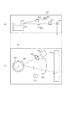
図1は本発明の実施形態に係る画像形成装置の断面図である。原稿スキャナ700は、プラテンガラス702上の画像を照明ランプ703、ミラー704A、B、C、及びレンズ705を介してカラーイメージセンサ706に結像して、原稿のカラー画像を、ブルー(B)、グリーン(G)、レッド(R)の色成分毎に読み取り、電気的な画像信号に変換する。そして、この原稿スキャナ700で得たB、G、Rの画像信号に対して色変換処理を行い、ブラック(K)、シアン(C)、マゼンタ(M)、イエロー(Y)のカラー画像データを得る。
FIG. 1 is a cross-sectional view of an image forming apparatus according to an embodiment of the present invention. The document scanner 700 forms an image on the platen glass 702 on the
プリンタ701では、レーザスキャナ707(符号に付されたM、C、Y、Kは画像形成する色を示す。以下同じ。)が、原稿スキャナ700からのカラー画像データに応じたレーザ光を発光して、原稿画像に対応した静電潜像を副走査方向に回転駆動される感光体708上に形成する。感光体708の周りには、帯電器709、現像器710、中間転写ベルト711、第1転写バイアスブレード712が設けられている。中間転写ベルト711は駆動ローラ713と、従動ローラ714、715に張架されている。また、第2転写バイアスローラ716は、中間転写ベルト711の従動ローラ714に対向する位置に配置されている。また、中間転写ベルト711の表面で従動ローラ715に対向する所定位置に、ベルトクリーニングユニット717が設けられている。感光体708上の静電潜像は現像器710により現像される。現像された感光体708上のトナー画像は第2転写バイアスローラ716により中間転写ベルト711に転写される。中間転写ベルト711上に転写されたトナー画像は第2転写バイアスローラ716によりカセット718から給紙された記録紙(記録シート)に転写される。記録紙上のトナー画像は定着器724により定着処理される。
In the
図2(a)はレーザスキャナ707の側面断面図、図2(b)はその上視断面図である。発光素子群800は、画像データに応じたレーザ光を発光する2つの発光源(副走査方向先頭から順に発光源A、B)を有する。発光素子群800は発光源A及びBにより2ライン分のレーザ光の発光を同時に行う。発光源A、Bから射出されるレーザ光の光路をそれぞれ実線、点線で表す。発光素子群800から射出された2つのレーザ光は光学系(レンズ801、ポリゴンミラー806、fθレンズ804、平面ミラー805)を介して感光体708の副走査方向に並べて感光体708に照射される。6面の反射面を側部に有するポリゴンミラー806はポリゴンモータ802により回転駆動される。ポリゴンミラー806が1回転すると、ポリゴンミラー806は発光素子群800のレーザ光を主走査方向に6回偏向走査する。検知素子803がポリゴンミラー806により偏向されたレーザ光を検知すると、検知素子803は各主走査の露光開始のトリガーとなるBD(BeamDetect)信号を出力する。
2A is a side sectional view of the
図3は原稿スキャナ700から出力された画像データを画像処理してレーザスキャナ707へ出力する画像処理部のブロック構成図である。読み取り画像処理部152は、イメージセンサ706から出力されるRGB信号に対して、シェーディング補正、色変換処理、ノイズ除去などを実施することにより、イメージセンサ706を含む光学系のバラツキや特性の補正を行う。コントローラ153は、読み取り画像処理部152から出力された画像データを受けて、必要に応じて画像圧縮をかけて、メモリ157に格納する。また、コントローラ153は、インターフェイス156を介してコンピュータから受信したデータを画像データに展開したり、モデム159を介して受信したファクシミリ画像を展開したりした後、メモリ157に格納する。また、コントローラ153は、メモリ157に一旦格納した画像を、ハードディスク158に格納することで、画像の入力順や出力順に拘束されない円滑なプリントを実現する。また、コントローラ153は、プリント時には、メモリ157またはハードディスク158に格納された画像データを書き込み画像処理部154に送る。書き込み画像処理部154は、RGBデータからYMCKデータへの変換や、プリンタの色域に合わせた変換、2次元的な周波数特性の補正、階調補正、階調数変換、解像度変換などの画像処理を行い、画像処理後の画像データをレーザスキャナ707に送る。レーザスキャナ707は、書き込み画像処理部154から画像データを受けて、画像データをPWM(パルス幅変調)信号に変換して、内部のレーザ駆動回路により発光源A及びBを駆動し、レーザ光を発光させ、感光体708上に潜像を形成する。
FIG. 3 is a block diagram of an image processing unit that performs image processing on the image data output from the document scanner 700 and outputs the image data to the
図4は書き込み画像処理部154のブロック構成図である。色空間変換部301は、各10bitのRGBデータ(輝度データ)を入力して、各10bitのYMCKデータ(濃度データ)に変換して出力する。補正部310は周波数特性補正、階調補正、階調数変換、走査線ピッチ補正を行う。周波数特性補正部311は、色毎の周波数特性の補正や、後段の階調数変換部313に適用される画像処理に合わせて適切な特性でフィルタリングする。階調補正部312は、後段の階調数変換部313と環境変動に応じて、テスト用のパターンなどからのフィードバックにより階調を調整する。レーザピッチ補正部314は、走査線ピッチの粗密によって生じる濃度ムラを補正する。
FIG. 4 is a block diagram of the write
図5は発光素子群800の発光源A及びBから射出されたレーザ光が光学系を介して感光体708上に照射された走査線を示す図である。一点鎖線は理想的な走査線、実線は発光源Aからのレーザ光による走査線、点線は発光源Bからのレーザ光による走査線を表す。発光源A及びBからのレーザ光による走査線は、光学系内の通過位置又は反射位置の違いによってそれぞれ異なる度合で湾曲する。その結果、発光源A及びBからのレーザ光による走査線には粗密ができてしまう。例えば、主走査位置X1において1走査目で発光源AとBがレーザ光を発光した場合、照射された2つのレーザスポットは理想よりも近づく(走査線間のピッチが密の状態となる)。一方、主走査位置X2において1走査目で発光源Bが2走査目で発光源Aがレーザ光を発光した場合、照射された2つのレーザスポットは理想よりも遠ざかる(走査線間のピッチが粗の状態となる)。
FIG. 5 is a diagram showing scanning lines in which the laser light emitted from the light emitting sources A and B of the light emitting
図6(a)は密の状態の2つのレーザスポットにより形成された潜像電位、図6(b)は粗の状態の2つのレーザスポットにより形成された潜像電位を示す図である。縦軸の下方向が副走査方向、横軸の右方向が感光体708の表面電位、横軸の左方向が現像により感光体708に付着するトナー付着量を示す。感光体708の表面がマイナスの高電圧により帯電された状態でレーザが照射されると、感光体708の表面電位が上昇し、潜像電位が形成される。潜像電位が閾値Vthを超えた部分には、現像処理によりトナーが付着する。発光源A及びBのレーザスポットが近接していると、2つの潜像電位の重なり度合に応じた合成潜像電位が形成される。密の状態の2つのレーザスポットにより潜像が形成される場合、図6(a)に示すように、それぞれの潜像電位の重なり部分が多くなるため、合成潜像電位が閾値Vthを超える領域が多くなる。その結果、副走査方向のトナー付着幅が広くなる。一方、粗の状態の2つのレーザスポットにより潜像が形成される場合、図6(b)に示すように、それぞれの潜像電位の重なり部分が少なくなるため、合成潜像電位が閾値Vthを超える領域が少なくなる。その結果、副走査方向のトナー付着幅が狭くなる。 FIG. 6A shows a latent image potential formed by two laser spots in a dense state, and FIG. 6B shows a latent image potential formed by two laser spots in a coarse state. The downward direction of the vertical axis indicates the sub-scanning direction, the right direction of the horizontal axis indicates the surface potential of the photoconductor 708, and the left direction of the horizontal axis indicates the amount of toner attached to the photoconductor 708 due to development. When the laser is irradiated while the surface of the photoconductor 708 is charged with a negative high voltage, the surface potential of the photoconductor 708 rises and a latent image potential is formed. Toner adheres to the portion where the latent image potential exceeds the threshold value Vth by development processing. When the laser spots of the light sources A and B are close to each other, a combined latent image potential corresponding to the overlapping degree of the two latent image potentials is formed. When a latent image is formed by two laser spots in a dense state, as shown in FIG. 6A, the overlapping portions of the latent image potentials increase, so that the region where the combined latent image potential exceeds the threshold value Vth Will increase. As a result, the toner adhesion width in the sub-scanning direction is widened. On the other hand, when a latent image is formed by two laser spots in a rough state, as shown in FIG. 6B, the overlapping portions of the latent image potentials are reduced, so that the combined latent image potential has a threshold value Vth. There are fewer areas to exceed. As a result, the toner adhesion width in the sub-scanning direction is narrowed.
図7(a)は理想的な距離の2つのレーザスポットによる潜像に付着したトナー領域、図7(b)は密の状態の2つのレーザスポットによる潜像に付着したトナー領域、図7(c)は粗の状態の2つのレーザスポットによる潜像に付着したトナー領域を示す図である。図中の濃い領域は潜像電位の重なりにより閾値Vthを越えた部分である。図からわかるように、2つのレーザスポットが密の場合はトナー領域が理想より大きく、粗の場合はトナー領域が理想より小さくなる。そこで、前述したレーザピッチ補正部314において、注目画素のレーザスポットと副走査方向の隣接画素のレーザスポットが密の場合には、画像データ中の注目画素の濃度を減少させ、注目画素のレーザスポットと副走査方向の隣接画素のレーザスポットが粗の場合には、画像データ中の注目画素の濃度を増加させる。すなわち、2つの発光源の光が感光体上で複数回走査されることにより感光体上に形成される複数の走査線間の粗密に応じて、画像データの濃度を増減する画像処理を行う。レーザピッチ補正部314から出力された画像データは、レーザスキャナ707でPWM変換されるため、各画素に対応したレーザスポットの主走査方向の幅は、各画素の値に対応した幅となる。従って、注目画素のレーザスポットと副走査方向の隣接画素のレーザスポットが密の場合には、レーザスポットの主走査方向の幅は縮小され、図7(b)の点線で示すようにトナー領域が縮小されて理想に近づけられる。また、注目画素のレーザスポットと副走査方向の隣接画素のレーザスポットが粗の場合には、レーザスポットの主走査方向の幅は拡大され、図7(c)の点線で示すようにトナー領域が拡大されて理想に近づけられる。
7A is a toner region attached to a latent image by two laser spots at an ideal distance, FIG. 7B is a toner region attached to a latent image by two laser spots in a dense state, and FIG. (c) is a diagram showing a toner region attached to a latent image by two laser spots in a rough state. The dark area in the figure is the part exceeding the threshold value Vth due to the overlapping of the latent image potential. As can be seen from the figure, when the two laser spots are dense, the toner area is larger than ideal, and when it is coarse, the toner area is smaller than ideal. Therefore, in the laser pitch correction unit 314 described above, when the laser spot of the target pixel and the laser spot of the adjacent pixel in the sub-scanning direction are dense, the density of the target pixel in the image data is decreased, and the laser spot of the target pixel is reduced. When the laser spot of adjacent pixels in the sub-scanning direction is rough, the density of the target pixel in the image data is increased. That is, image processing for increasing or decreasing the density of image data is performed according to the density between a plurality of scanning lines formed on the photosensitive member by scanning the light of the two light emitting sources a plurality of times on the photosensitive member. Since the image data output from the laser pitch correction unit 314 is PWM-converted by the
図8はレーザピッチ補正部314のブロック構成図である。レーザピッチ補正部314に入力された3ライン分の画像データがフィルタ演算部103に入力される。N−1ライン目の画像データIMAGE_L2はラインメモリ102を介して、Nライン目の画像データIMAGE_L1はラインメモリ101を介して、N+1ライン目の画像データIMAGE_INは直接フィルタ演算部103に入力される。ラインメモリ101及び102はそれぞれ1主走査ライン分の画像データを記憶できる。画素カウンタ110は、フィルタ演算部103がフィルタ演算すべき画素(注目画素)の主走査位置情報を出力するものであり、画像データIMAGE_INを転送するための画素単位のクロックに応じてカウントアップし、1主走査ラインの最終画素までカウントアップされるとリセットされる。フィルタ演算部103は、Nライン目の画像データのうち画素カウンタ110が示す主走査位置の画素を注目画素として、注目画素の値に対して隣接画素(N−1ライン目とN+1ライン目)の値とフィルタ係数を用いたフィルタ演算を行う。具体的には、フィルタ演算部103は、次式を用いて、Nライン目の画像データIMAGE_L1、N−1ライン目の画像データIMAGE_L2、フィルタ係数K2、N+1ライン目の画像データIMAGE_IN、フィルタ係数K0に基づくフィルタ演算を行い、演算後の画像データIMAGE_OUTを出力する。
IMAGE_OUT=IMAGE_IN×K0+IMAGE_L1+IMAGE_L2×K2
フィルタ係数K2は、N−1ライン目の隣接画素のレーザスポットと注目画素のレーザスポットが理想よりも近い場合には負の値をとり、理想よりも遠い場合には正の値をとる。同様に、フィルタ係数K0は、N+1ライン目の隣接画素のレーザスポットと注目画素のレーザスポットが理想よりも近い場合には負の値をとり、理想よりも遠い場合には正の値をとる。つまり、隣接画素のレーザスポットと注目画素のレーザスポットが理想よりも近い(走査線間のピッチが密)場合には、注目画素の濃度を減少させ、隣接画素のレーザスポットと注目画素のレーザスポットが理想よりも遠い(走査線間のピッチが粗)場合には、注目画素の濃度を増加させる。このようにして、注目画素の画像データIMAGE_L1は、副走査方向の隣接画素のレーザスポットとの粗密の度合、及び、副走査方向の隣接画素の画像データIMAGE_L2,IMAGE_INに応じて増減され、画像データIMAGE_OUTとして出力される。
FIG. 8 is a block diagram of the laser pitch correction unit 314. The image data for three lines input to the laser pitch correction unit 314 is input to the filter calculation unit 103. The image data IMAGE_L2 of the (N-1) th line is input to the filter operation unit 103 via the
IMAGE_OUT = IMAGE_IN × K0 + IMAGE_L1 + IMAGE_L2 × K2
The filter coefficient K2 takes a negative value when the laser spot of the adjacent pixel on the (N−1) th line and the laser spot of the target pixel are closer than ideal, and takes a positive value when farther than ideal. Similarly, the filter coefficient K0 takes a negative value when the laser spot of the adjacent pixel on the (N + 1) th line and the laser spot of the pixel of interest are closer than ideal, and takes a positive value when farther than ideal. That is, when the laser spot of the adjacent pixel and the laser spot of the target pixel are closer than ideal (the pitch between the scanning lines is dense), the density of the target pixel is decreased, and the laser spot of the adjacent pixel and the laser spot of the target pixel are reduced. Is farther than ideal (the pitch between scan lines is coarse), the density of the pixel of interest is increased. In this way, the image data IMAGE_L1 of the target pixel is increased or decreased according to the degree of density with the laser spot of the adjacent pixel in the sub-scanning direction and the image data IMAGE_L2 and IMAGE_IN of the adjacent pixel in the sub-scanning direction. Output as IMAGE_OUT.
フィルタ係数制御部104は、注目画素と隣接画素のレーザスポット間距離に対応するフィルタ係数K0及びK2を、フィルタ係数テーブル105を参照して求めて、フィルタ演算部103に供給する。フィルタ係数制御部104は、注目画素と隣接画素のレーザスポット間距離を、理想のレーザスポット間距離と、注目画素のレーザスポットの理想位置からのズレ量と、隣接画素のレーザスポットの理想位置からのズレ量とから求める。 The filter coefficient control unit 104 obtains filter coefficients K0 and K2 corresponding to the distance between the laser spots of the target pixel and adjacent pixels with reference to the filter coefficient table 105, and supplies the filter coefficients to the filter calculation unit 103. The filter coefficient control unit 104 determines the distance between the laser spot of the target pixel and the adjacent pixel from the ideal distance between the laser spots, the amount of deviation from the ideal position of the laser spot of the target pixel, and the ideal position of the laser spot of the adjacent pixel. Calculate from the amount of deviation.
図9は注目画素と隣接画素のレーザスポット間距離の求め方を説明する図である。図9(a)は理想のレーザスポット間距離Dを示す。図9(b)は、注目画素のレーザが発光源Aにより発光される場合の、注目画素と隣接画素のレーザスポット間距離の求め方を示す。ズレ量SA及びSBは、それぞれ発光源A及びBのレーザスポットの理想位置からのズレ量を表し、図9の上方向(副走査方向と逆方向)のズレを正、下方向(副走査方向)のズレを負で表す。注目画素と上側の隣接画素のレーザスポット間距離はD+(SB−SA)で求められ、注目画素と下側の隣接画素のレーザスポット間距離はD+(SA−SB)で求められる。図9(c)は、注目画素のレーザが発光源Bにより発光される場合の、注目画素と隣接画素のレーザスポット間距離の求め方を示す。注目画素と上側の隣接画素のレーザスポット間距離はD+(SA−SB)で求められ、注目画素と下側の隣接画素のレーザスポット間距離はD+(SB−SA)で求められる。ズレ量SA及びSBはそれぞれ、ズレ量演算部A106及びズレ量演算部B108がプロファイルメモリA107及びプロファイルメモリB109を参照しながら求められ、フィルタ係数制御部104に供給される。フィルタ係数制御部104は、ズレ量SA及びSBと前述の式によって、注目画素と隣接画素のレーザスポット間距離を求める。 FIG. 9 is a diagram for explaining how to obtain the distance between the laser spot of the target pixel and the adjacent pixel. FIG. 9A shows an ideal distance D between laser spots. FIG. 9B shows how to obtain the distance between the laser spot of the pixel of interest and the adjacent pixel when the laser of the pixel of interest emits light from the light source A. The shift amounts SA and SB represent the shift amounts from the ideal positions of the laser spots of the light sources A and B, respectively, and the shift in the upper direction (the reverse direction to the sub-scanning direction) in FIG. ) Is negative. The distance between the laser spot of the target pixel and the upper adjacent pixel is obtained by D + (SB−SA), and the distance between the laser spot of the target pixel and the lower adjacent pixel is obtained by D + (SA−SB). FIG. 9C shows how to obtain the distance between the laser spot of the target pixel and the adjacent pixel when the laser of the target pixel emits light from the light emission source B. The distance between the laser spot of the target pixel and the upper adjacent pixel is obtained by D + (SA−SB), and the distance between the laser spots of the target pixel and the lower adjacent pixel is obtained by D + (SB−SA). The deviation amounts SA and SB are obtained by the deviation amount calculation unit A106 and the deviation amount calculation unit B108 with reference to the profile memory A107 and the profile memory B109, respectively, and are supplied to the filter coefficient control unit 104. The filter coefficient control unit 104 obtains the distance between the laser spot of the target pixel and the adjacent pixel based on the shift amounts SA and SB and the above-described formula.
ズレ量演算部A106及びズレ量演算部B108は、発光源A及びBの走査線プロファイルに基づいてズレ量SA及びSBを求める。図10は発光源A及びBの走査線プロファイルを示す図である。実際の発光源A及びBの走査線プロファイルは曲線であるが、プロファイルメモリに記憶させるデータ量を減らすために、プロファイル曲線を1次スプライン補間で直線近似し、変化点のプロファイルデータのみをプロファイルメモリA107及びプロファイルメモリB109に記憶させておく。図11はプロファイルメモリA107及びプロファイルメモリB109に記憶された走査線プロファイルデータ(変化点の座標データと変化率データ)を示す図である。図10からわかるように、各主走査位置におけるズレ量SAは、変化点の座標データXAn及びYAnと変化率データMAn/NAnに基づいて次式により求められ、同様にズレ量SBは、変化点の座標データXBn及びYBnと変化率データMBn/NBnに基づいて次式により求められる。YAnは発光源Aのレーザスポットの主走査位置XAnでのズレ量、YBnは発光源Bのレーザスポットの主走査位置XBnでのズレ量である。また、Xは画素カウンタ110のカウント値が示す主走査位置である。XAnは、XAn≦X<XAn+1を満たすXAnが用いられる。ズレ量演算部A106及びズレ量演算部B108は、プロファイルメモリA107及びプロファイルメモリB109からプロファイルデータを読み出して次式によりズレ量SA及びSBを求める。
SA=YAn+(MAn/NAn)×(X−XAn)
SB=YBn+(MBn/NBn)×(X−XBn)
The deviation amount
SA = YAn + (MAn / NAn) × (X−XAn)
SB = YBn + (MBn / NBn) × (X−XBn)
発光素子群800の発光源A及びBの走査線プロファイルは、画像形成装置の製造過程において個体毎に測定され、コントローラ153により走査線プロファイルデータがプロファイルメモリA107及びプロファイルメモリB109に書き込まれる。プロファイルメモリA107及びプロファイルメモリB109は不揮発性メモリである。図12は発光源A及びBのプロファイルを測定するためのパッチ検知センサ901の外観図である。パッチ検知センサ901は、画像形成装置の製造過程におけるプロファイル測定時に一時的に、感光体708M、708C、708Y、708Kの近傍にそれぞれ取り付けられ、コントローラ153に電気的に接続される。ラインセンサ902は感光体708の主走査左端上のパッチ画像を、ラインセンサ903は感光体708の主走査中央部上のパッチ画像を、ラインセンサ904は感光体708の主走査右端上のパッチ画像を読み取り、これらの画像データをコントローラ153に出力する。コントローラ153は、主走査方向の左端部、中央部、右端部にパッチ画像(四角形の単一濃度)を感光体708上に形成させる。このとき、コントローラ153は3つのパッチ画像を理論上同一の副走査位置に形成させ、パッチ検知センサ901から出力されるそれぞれのパッチ画像の副走査位置から2次関数で近似することによりプロファイルを求める。プロファイルを測定する際、発光源A及びBのプロファイルをそれぞれ測定するため、コントローラ153は発光源Aのみを用いたパッチ画像形成及びパッチ画像検知と発光源Bのみを用いたパッチ画像形成及びパッチ画像検知をそれぞれ行う。発光源A及びBのプロファイルを求めたコントローラ153は、プロファイルデータをプロファイルメモリA107及びプロファイルメモリB109に書き込む。
The scanning line profiles of the light sources A and B of the light emitting
上述の実施形態では、発光素子群800の発光源数は2つであったが、本発明は3つ以上の発光源を有する画像形成装置にも適用することができる。
In the above-described embodiment, the number of light emitting sources in the light emitting
800 発光素子群
314 レーザピッチ補正部
103 フィルタ演算部
800 Light Emitting Element Group 314 Laser Pitch Correction Unit 103 Filter Operation Unit
Claims (4)
前記複数の光ビームが前記感光体上を走査するように、前記複数の光ビームを偏向する偏向部と、
前記偏向された複数の光ビームが通過するレンズと、
前記レンズを通過した前記複数の光ビームによって露光される前記感光体と、
前記光ビームが走査する方向に対応する主走査方向における注目画素の位置情報に応じて、第1および第2のフィルタ係数を含むフィルタ係数を設定する設定手段と、
前記主走査方向に直交する副走査方向において前記注目画素の上流側に位置する周辺画素の値と前記第1フィルタ係数との演算の結果、および該副走査方向において該注目画素の下流側に位置する周辺画素の値と前記第2フィルタ係数との演算の結果を用いて、該注目画素の値を修正するフィルタ処理手段と、
前記修正された注目画素の値に応じて前記光源を駆動する駆動手段とを有し、
前記第1のフィルタ係数は、前記主走査方向における前記注目画素の位置における、前記注目画素に対応する光ビームの露光位置と前記注目画素の上流側に位置する周辺画素に対応する光ビームの露光位置との間隔である第1間隔に応じており、前記第2のフィルタ係数は、前記注目画素に対応する光ビームの露光位置と前記注目画素の下流側に位置する周辺画素に対応する光ビームの露光位置との間隔である第2間隔に応じている
ことを特徴とする画像形成装置。 A plurality of light sources for emitting a plurality of light beams for exposing one photosensitive member;
A deflecting unit that deflects the plurality of light beams such that the plurality of light beams scan on the photosensitive member;
A lens through which the deflected light beams pass;
The photoreceptor exposed by the plurality of light beams that have passed through the lens;
Setting means for setting a filter coefficient including first and second filter coefficients in accordance with position information of a target pixel in a main scanning direction corresponding to a direction in which the light beam scans;
The result of the calculation of the value of the peripheral pixel located upstream of the target pixel and the first filter coefficient in the sub-scanning direction orthogonal to the main scanning direction, and the downstream position of the target pixel in the sub-scanning direction Filter processing means for correcting the value of the target pixel using the result of the operation of the value of the surrounding pixel and the second filter coefficient;
Driving means for driving the light source in accordance with the corrected value of the target pixel;
The first filter coefficient is an exposure position of a light beam corresponding to the target pixel at a position of the target pixel in the main scanning direction and an exposure of a light beam corresponding to a peripheral pixel located upstream of the target pixel. The second filter coefficient is a light beam corresponding to an exposure position of a light beam corresponding to the pixel of interest and a peripheral pixel located downstream of the pixel of interest. An image forming apparatus according to claim 2, wherein the second interval is an interval from the exposure position.
前記プロファイルと前記注目画素の位置情報とに基づき、前記第1間隔および前記第2間隔を算出する算出手段とを有し、
前記プロファイルは該プロファイルが対応する前記光源から出射される光ビームの走査線の湾曲特性を示すことを特徴とする請求項1記載の画像形成装置。 Holding means for holding a profile corresponding to each of the plurality of light sources;
Calculation means for calculating the first interval and the second interval based on the profile and position information of the pixel of interest;
The image forming apparatus according to claim 1, wherein the profile indicates a curve characteristic of a scanning line of a light beam emitted from the light source corresponding to the profile.
前記光ビームが走査する方向に対応する主走査方向における注目画素の位置情報に応じて、第1および第2のフィルタ係数を含むフィルタ係数を設定し、
前記主走査方向に直交する副走査方向において前記注目画素の上流側に位置する周辺画素の値と前記第1フィルタ係数との演算の結果、および該副走査方向において該注目画素の下流側に位置する周辺画素の値と前記第2フィルタ係数との演算の結果を用いて、該注目画素の値を修正するフィルタ処理する画像処理方法であり、
前記第1のフィルタ係数は、前記主走査方向における前記注目画素の位置における、前記注目画素に対応する光ビームの露光位置と前記注目画素の上流側に位置する周辺画素に対応する光ビームの露光位置との間隔である第1間隔に応じており、前記第2のフィルタ係数は、前記注目画素に対応する光ビームの露光位置と前記注目画素の下流側に位置する周辺画素に対応する光ビームの露光位置との間隔である第2間隔に応じている
ことを特徴とする画像処理方法。 A plurality of light sources for emitting a plurality of light beams for exposing one photosensitive member; a deflecting unit for deflecting the plurality of light beams so that the plurality of light beams scan on the photosensitive member; An image processing method for an image forming apparatus, comprising: a lens through which the plurality of light beams passed, and the photoconductor exposed by the plurality of light beams that have passed through the lens,
According to the position information of the pixel of interest in the main scanning direction corresponding to the direction in which the light beam scans, a filter coefficient including first and second filter coefficients is set,
The result of the calculation of the value of the peripheral pixel located upstream of the target pixel and the first filter coefficient in the sub-scanning direction orthogonal to the main scanning direction, and the downstream position of the target pixel in the sub-scanning direction An image processing method for performing a filter process for correcting the value of the target pixel using the result of the calculation of the value of the surrounding pixel and the second filter coefficient,
The first filter coefficient is an exposure position of a light beam corresponding to the target pixel at a position of the target pixel in the main scanning direction and an exposure of a light beam corresponding to a peripheral pixel located upstream of the target pixel. The second filter coefficient is a light beam corresponding to an exposure position of a light beam corresponding to the pixel of interest and a peripheral pixel located downstream of the pixel of interest. An image processing method according to claim 2, wherein the second interval is an interval from the exposure position.
Priority Applications (5)
| Application Number | Priority Date | Filing Date | Title |
|---|---|---|---|
| JP2009270102A JP5744391B2 (en) | 2009-11-27 | 2009-11-27 | Image forming apparatus |
| KR1020100115737A KR101401750B1 (en) | 2009-11-27 | 2010-11-19 | Image forming apparatus and image processing method |
| EP10191807.6A EP2333617B1 (en) | 2009-11-27 | 2010-11-19 | Image forming apparatus |
| US12/954,172 US9308743B2 (en) | 2009-11-27 | 2010-11-24 | Image forming apparatus |
| CN201010568503.0A CN102081229B (en) | 2009-11-27 | 2010-11-26 | Image forming apparatus |
Applications Claiming Priority (1)
| Application Number | Priority Date | Filing Date | Title |
|---|---|---|---|
| JP2009270102A JP5744391B2 (en) | 2009-11-27 | 2009-11-27 | Image forming apparatus |
Publications (3)
| Publication Number | Publication Date |
|---|---|
| JP2011110846A JP2011110846A (en) | 2011-06-09 |
| JP2011110846A5 JP2011110846A5 (en) | 2013-03-21 |
| JP5744391B2 true JP5744391B2 (en) | 2015-07-08 |
Family
ID=43708941
Family Applications (1)
| Application Number | Title | Priority Date | Filing Date |
|---|---|---|---|
| JP2009270102A Active JP5744391B2 (en) | 2009-11-27 | 2009-11-27 | Image forming apparatus |
Country Status (5)
| Country | Link |
|---|---|
| US (1) | US9308743B2 (en) |
| EP (1) | EP2333617B1 (en) |
| JP (1) | JP5744391B2 (en) |
| KR (1) | KR101401750B1 (en) |
| CN (1) | CN102081229B (en) |
Families Citing this family (7)
| Publication number | Priority date | Publication date | Assignee | Title |
|---|---|---|---|---|
| JP5930750B2 (en) * | 2012-02-10 | 2016-06-08 | キヤノン株式会社 | Image forming apparatus and image forming method |
| WO2015010865A1 (en) | 2013-07-22 | 2015-01-29 | Harman Becker Automotive Systems Gmbh | Automatic timbre control |
| EP3025516B1 (en) | 2013-07-22 | 2020-11-04 | Harman Becker Automotive Systems GmbH | Automatic timbre, loudness and equalization control |
| JP6821341B2 (en) * | 2015-07-16 | 2021-01-27 | キヤノン株式会社 | Image forming device |
| JP6723848B2 (en) * | 2015-07-16 | 2020-07-15 | キヤノン株式会社 | Image forming device |
| JP6611510B2 (en) * | 2015-08-05 | 2019-11-27 | キヤノン株式会社 | Correction method for image forming apparatus |
| JP6632393B2 (en) * | 2016-01-25 | 2020-01-22 | キヤノン株式会社 | Image forming device |
Family Cites Families (17)
| Publication number | Priority date | Publication date | Assignee | Title |
|---|---|---|---|---|
| US4887225A (en) * | 1985-05-24 | 1989-12-12 | Danippon Screen Mfg. Co., Ltd. | Method and device for controlling exposure beams |
| JP2575849B2 (en) * | 1988-11-14 | 1997-01-29 | 富士写真フイルム株式会社 | Image exposure method and apparatus |
| JPH0816737B2 (en) | 1990-06-08 | 1996-02-21 | キヤノン株式会社 | Image processing device |
| JPH09109458A (en) * | 1995-08-11 | 1997-04-28 | Hitachi Koki Co Ltd | Electrophotographic apparatus |
| JP3562263B2 (en) * | 1997-10-27 | 2004-09-08 | 富士ゼロックス株式会社 | Multicolor image forming device |
| US7003241B1 (en) * | 1998-07-31 | 2006-02-21 | Ricoh Printing Systems, Ltd. | Image recording device and an image recording system |
| JP2000238329A (en) * | 1999-02-24 | 2000-09-05 | Fuji Xerox Co Ltd | Image-forming apparatus |
| US7030899B2 (en) * | 2001-07-19 | 2006-04-18 | Konica Corporation | Image-forming apparatus having function of preventing unevenness of image formed on recording medium |
| US7206014B2 (en) * | 2001-07-24 | 2007-04-17 | Ricoh Company, Ltd. | Multi-beam pitch adjusting apparatus and image forming apparatus |
| JP3600228B2 (en) * | 2002-03-01 | 2004-12-15 | 株式会社リコー | Optical scanning device and image forming apparatus |
| JP2006150772A (en) * | 2004-11-30 | 2006-06-15 | Kyocera Mita Corp | Imaging device |
| US7508407B2 (en) * | 2005-05-31 | 2009-03-24 | Seiko Epson Corporation | Light scanning apparatus, image forming apparatus equipped with such light scanning apparatus, and control method or image forming method for such image forming apparatus |
| US7548252B2 (en) * | 2006-02-16 | 2009-06-16 | Canon Kabushiki Kaisha | Optical scanning apparatus and color image forming apparatus using the same |
| JP4942176B2 (en) * | 2006-11-01 | 2012-05-30 | キヤノン株式会社 | Image forming apparatus and control method thereof |
| US8149258B2 (en) * | 2007-06-29 | 2012-04-03 | Canon Kabushiki Kaisha | Image forming apparatus and control method |
| JP2009039945A (en) * | 2007-08-08 | 2009-02-26 | Canon Inc | Image forming apparatus, its control method and control program |
| JP5369935B2 (en) * | 2008-09-05 | 2013-12-18 | 株式会社リコー | Image forming apparatus |
-
2009
- 2009-11-27 JP JP2009270102A patent/JP5744391B2/en active Active
-
2010
- 2010-11-19 EP EP10191807.6A patent/EP2333617B1/en active Active
- 2010-11-19 KR KR1020100115737A patent/KR101401750B1/en active IP Right Grant
- 2010-11-24 US US12/954,172 patent/US9308743B2/en active Active
- 2010-11-26 CN CN201010568503.0A patent/CN102081229B/en active Active
Also Published As
| Publication number | Publication date |
|---|---|
| EP2333617A2 (en) | 2011-06-15 |
| EP2333617B1 (en) | 2019-07-10 |
| KR101401750B1 (en) | 2014-05-30 |
| KR20110059536A (en) | 2011-06-02 |
| CN102081229A (en) | 2011-06-01 |
| CN102081229B (en) | 2015-06-03 |
| EP2333617A3 (en) | 2016-09-07 |
| US9308743B2 (en) | 2016-04-12 |
| US20110128344A1 (en) | 2011-06-02 |
| JP2011110846A (en) | 2011-06-09 |
Similar Documents
| Publication | Publication Date | Title |
|---|---|---|
| JP5744391B2 (en) | Image forming apparatus | |
| US7746370B2 (en) | Image forming apparatus and method of controlling same | |
| JP4065533B2 (en) | Modulator | |
| KR20150142022A (en) | Image formation device | |
| US7405743B2 (en) | Image forming method and apparatus | |
| JP5515893B2 (en) | Optical writing apparatus, image forming apparatus, and control method of optical writing apparatus | |
| JP5484614B2 (en) | Image forming apparatus | |
| US9904206B2 (en) | Image forming apparatus | |
| JP4667201B2 (en) | Image forming apparatus and control method thereof | |
| JP7191716B2 (en) | image forming device | |
| JP5917081B2 (en) | Image forming apparatus | |
| JP4612857B2 (en) | Image forming apparatus and image distortion correction method | |
| JP6760013B2 (en) | Image forming device | |
| JP4939660B2 (en) | Image forming apparatus and control method thereof | |
| JP5188097B2 (en) | Image forming apparatus | |
| JP6136391B2 (en) | Image processing apparatus, image forming apparatus, image correction method, and program | |
| JP6091685B2 (en) | Image forming apparatus | |
| JP2022012828A (en) | Image formation apparatus | |
| JP5621863B2 (en) | Image forming apparatus, streak determination method, and streak determination program in image forming apparatus | |
| US20050062837A1 (en) | Method and apparatus for controlling a laser scanning unit | |
| JP2007316121A (en) | Color image forming apparatus, image forming method and program | |
| JP2011007980A (en) | Image forming apparatus | |
| JP2017201374A (en) | Image forming apparatus and image processing apparatus | |
| JP2006088567A (en) | Image forming apparatus | |
| JP2014148169A (en) | Image formation device |
Legal Events
| Date | Code | Title | Description |
|---|---|---|---|
| A621 | Written request for application examination |
Free format text: JAPANESE INTERMEDIATE CODE: A621 Effective date: 20121127 |
|
| A521 | Request for written amendment filed |
Free format text: JAPANESE INTERMEDIATE CODE: A523 Effective date: 20130131 |
|
| A977 | Report on retrieval |
Free format text: JAPANESE INTERMEDIATE CODE: A971007 Effective date: 20130924 |
|
| A131 | Notification of reasons for refusal |
Free format text: JAPANESE INTERMEDIATE CODE: A131 Effective date: 20131001 |
|
| A521 | Request for written amendment filed |
Free format text: JAPANESE INTERMEDIATE CODE: A523 Effective date: 20131202 |
|
| A131 | Notification of reasons for refusal |
Free format text: JAPANESE INTERMEDIATE CODE: A131 Effective date: 20140819 |
|
| TRDD | Decision of grant or rejection written | ||
| A01 | Written decision to grant a patent or to grant a registration (utility model) |
Free format text: JAPANESE INTERMEDIATE CODE: A01 Effective date: 20150407 |
|
| A61 | First payment of annual fees (during grant procedure) |
Free format text: JAPANESE INTERMEDIATE CODE: A61 Effective date: 20150430 |
|
| R151 | Written notification of patent or utility model registration |
Ref document number: 5744391 Country of ref document: JP Free format text: JAPANESE INTERMEDIATE CODE: R151 |