JP2004157522A - Image generating device, image display device, image display method, and device for adjusting optical modulation element - Google Patents
Image generating device, image display device, image display method, and device for adjusting optical modulation element Download PDFInfo
- Publication number
- JP2004157522A JP2004157522A JP2003319971A JP2003319971A JP2004157522A JP 2004157522 A JP2004157522 A JP 2004157522A JP 2003319971 A JP2003319971 A JP 2003319971A JP 2003319971 A JP2003319971 A JP 2003319971A JP 2004157522 A JP2004157522 A JP 2004157522A
- Authority
- JP
- Japan
- Prior art keywords
- light
- light modulation
- modulation element
- image display
- drive signal
- Prior art date
- Legal status (The legal status is an assumption and is not a legal conclusion. Google has not performed a legal analysis and makes no representation as to the accuracy of the status listed.)
- Pending
Links
Images


Classifications
-
- G—PHYSICS
- G09—EDUCATION; CRYPTOGRAPHY; DISPLAY; ADVERTISING; SEALS
- G09G—ARRANGEMENTS OR CIRCUITS FOR CONTROL OF INDICATING DEVICES USING STATIC MEANS TO PRESENT VARIABLE INFORMATION
- G09G3/00—Control arrangements or circuits, of interest only in connection with visual indicators other than cathode-ray tubes
- G09G3/20—Control arrangements or circuits, of interest only in connection with visual indicators other than cathode-ray tubes for presentation of an assembly of a number of characters, e.g. a page, by composing the assembly by combination of individual elements arranged in a matrix no fixed position being assigned to or needed to be assigned to the individual characters or partial characters
- G09G3/34—Control arrangements or circuits, of interest only in connection with visual indicators other than cathode-ray tubes for presentation of an assembly of a number of characters, e.g. a page, by composing the assembly by combination of individual elements arranged in a matrix no fixed position being assigned to or needed to be assigned to the individual characters or partial characters by control of light from an independent source
-
- G—PHYSICS
- G02—OPTICS
- G02B—OPTICAL ELEMENTS, SYSTEMS OR APPARATUS
- G02B26/00—Optical devices or arrangements for the control of light using movable or deformable optical elements
- G02B26/08—Optical devices or arrangements for the control of light using movable or deformable optical elements for controlling the direction of light
- G02B26/10—Scanning systems
- G02B26/105—Scanning systems with one or more pivoting mirrors or galvano-mirrors
-
- G—PHYSICS
- G09—EDUCATION; CRYPTOGRAPHY; DISPLAY; ADVERTISING; SEALS
- G09G—ARRANGEMENTS OR CIRCUITS FOR CONTROL OF INDICATING DEVICES USING STATIC MEANS TO PRESENT VARIABLE INFORMATION
- G09G3/00—Control arrangements or circuits, of interest only in connection with visual indicators other than cathode-ray tubes
- G09G3/001—Control arrangements or circuits, of interest only in connection with visual indicators other than cathode-ray tubes using specific devices not provided for in groups G09G3/02 - G09G3/36, e.g. using an intermediate record carrier such as a film slide; Projection systems; Display of non-alphanumerical information, solely or in combination with alphanumerical information, e.g. digital display on projected diapositive as background
- G09G3/002—Control arrangements or circuits, of interest only in connection with visual indicators other than cathode-ray tubes using specific devices not provided for in groups G09G3/02 - G09G3/36, e.g. using an intermediate record carrier such as a film slide; Projection systems; Display of non-alphanumerical information, solely or in combination with alphanumerical information, e.g. digital display on projected diapositive as background to project the image of a two-dimensional display, such as an array of light emitting or modulating elements or a CRT
-
- G—PHYSICS
- G09—EDUCATION; CRYPTOGRAPHY; DISPLAY; ADVERTISING; SEALS
- G09G—ARRANGEMENTS OR CIRCUITS FOR CONTROL OF INDICATING DEVICES USING STATIC MEANS TO PRESENT VARIABLE INFORMATION
- G09G2310/00—Command of the display device
- G09G2310/02—Addressing, scanning or driving the display screen or processing steps related thereto
- G09G2310/0235—Field-sequential colour display
-
- G—PHYSICS
- G09—EDUCATION; CRYPTOGRAPHY; DISPLAY; ADVERTISING; SEALS
- G09G—ARRANGEMENTS OR CIRCUITS FOR CONTROL OF INDICATING DEVICES USING STATIC MEANS TO PRESENT VARIABLE INFORMATION
- G09G2320/00—Control of display operating conditions
- G09G2320/02—Improving the quality of display appearance
- G09G2320/0233—Improving the luminance or brightness uniformity across the screen
Abstract
Description
本発明は、例えば、光を回折又は反射させる回折格子型光バルブなどの光回折変調素子を用いて二次元画像を生成あるいは表示する画像生成装置、画像表示装置、画像表示方法、および光変調素子調整装置に関する。 The present invention provides, for example, an image generation device, an image display device, an image display method, and a light modulation device that generate or display a two-dimensional image using a light diffraction modulation device such as a diffraction grating light valve that diffracts or reflects light. It relates to an adjusting device.
プロジェクターやプリンターなどの画像形成装置において、画像の解像度を上げるには、1次元の画像表示素子からの光束を光走査手段で走査しながら画像形成手段に投影し、2次元画像を形成する方法が知られている(例えば、特許文献1参照)。1次元の画像表示素子として、米国Silicon Light Machine社が開発した回折ライト・バルブ(GLV: Grating Light Valve)が知られている(例えば、特許文献2、特許文献3参照)。
GLVは光の回折を利用したマイクロマシン位相反射型回折格子より成っている。GLVを用いれば、光の階調を電気的にコントロールすることにより画像表示が可能となる。
In order to increase the resolution of an image in an image forming apparatus such as a projector or a printer, there is a method of forming a two-dimensional image by projecting a light beam from a one-dimensional image display element onto an image forming unit while scanning the light beam with an optical scanning unit. It is known (for example, see Patent Document 1). As a one-dimensional image display element, a diffractive light valve (GLV: Grating Light Valve) developed by Silicon Light Machine Company in the United States is known (for example, see
The GLV is composed of a micromachined phase reflection type diffraction grating utilizing light diffraction. When the GLV is used, an image can be displayed by electrically controlling the gradation of light.
例えば、GLVにおいて、数μmのリボン電極数本で1画素を形成する画素素子とし、その画素素子を1次元方向に数百〜数千個配置する。当該複数の画素素子からなる1次元画像素子GLVは1次元空間変調器として機能し、1次元方向に集光した照明光をGLVにて変調した後にガルバノミラー(ポリゴンミラー)等で水平方向に走査することによって、2次元表示画像は形成される。
通常の2次元表示装置と比較して、GLVを用いた場合は、画面の縦方向の画素数は1次元方向の画素数と同じになるが、横方向は少なくとも1画素幅あれば良いので、2次元画像表示に必要な画素(ピクセル)数は少なくて済む。また、GLVの能動領域は、その寸法を小さく構成することが可能であり、高い解像度、高速なスイッチング速度及び広い帯域幅の表示が可能である一方、低い印加電圧で動作されるので、非常に小型化された表示装置を実現することが期待されている。
For example, in a GLV, a pixel element is formed to form one pixel with several ribbon electrodes of several μm, and several hundred to several thousand pixel elements are arranged in a one-dimensional direction. The one-dimensional image element GLV including the plurality of pixel elements functions as a one-dimensional spatial modulator, and the illumination light condensed in the one-dimensional direction is modulated by the GLV and then horizontally scanned by a galvanometer mirror (polygon mirror) or the like. By doing so, a two-dimensional display image is formed.
Compared to a normal two-dimensional display device, when GLV is used, the number of pixels in the vertical direction of the screen is the same as the number of pixels in the one-dimensional direction, but at least one pixel width in the horizontal direction is sufficient. The number of pixels required for displaying a two-dimensional image is small. In addition, the active area of the GLV can be configured to have a small size, and a high resolution, a high switching speed, and a wide bandwidth can be displayed. It is expected to realize a miniaturized display device.
このような1次元画像表示素子GLVを用いた画像表示装置は、通常の二次元画像表示装置、例えば、液晶パネルなどを用いた投射型表示装置と比べて、GLV自体に画素間の境界が存在しないため、極めて滑らかで自然な画像表現が可能である。さらに、三原色である赤色、緑色、青色のレーザを光源とし、これらの光を混合することで、極めて広い、自然な色再現範囲の画像が表現できるなど、従来にない優れた表示性能を有している。
しかし、実際に、例えば、1080画素素子を含むGLVをスキャンして得た1080×1920画素の画像表示装置において、良好な画像表示を全画素で実現することは容易ではない。その理由は、通常デバイス製造上画素素子を構成するリボン電極の形状や表面状態を表示領域全体に対して均一に作製することが難しい。そのため素子を動作させない状態でもnm程度の凹凸が発生するため、変調器としてのGLVは、画素素子ごとに変調特性(駆動電圧−変調光輝度)が変動する。その結果、画面上に輝度の不均一性が生じ、例えば、均一な黒画像を得ることが出来ない問題があった。
また、画素毎に設けられ、輝度の階調を調整する駆動回路特性自体にバラツキが存在するため、画素素子の変調特性を均一にすることも容易ではない。例えば、リボン電極をnmレベルで移動させる駆動信号の誤差により、GLVの可動リボン電極の移動量がばらつき、画素素子変調特性の変動を生じる。
以上のような変調特性のバラツキが表示画像上1画素から数画素単位の横縞として認識され画質の劣化を招いていた。
However, in practice, for example, in an image display device of 1080 × 1920 pixels obtained by scanning a GLV including 1080 pixel elements, it is not easy to realize good image display with all pixels. The reason is that it is usually difficult to uniformly manufacture the shape and the surface state of the ribbon electrode constituting the pixel element over the entire display region in device manufacturing. Therefore, unevenness of about nm occurs even in a state where the element is not operated, so that the modulation characteristic (drive voltage-modulated light luminance) of the GLV as a modulator varies for each pixel element. As a result, non-uniformity of luminance occurs on the screen, and for example, there is a problem that a uniform black image cannot be obtained.
In addition, since there is variation in the characteristics of a driving circuit that is provided for each pixel and adjusts the gradation of luminance, it is not easy to make the modulation characteristics of the pixel elements uniform. For example, due to an error in a drive signal for moving the ribbon electrode at the nm level, the amount of movement of the movable ribbon electrode of the GLV fluctuates, causing fluctuations in pixel element modulation characteristics.
The variation in the modulation characteristics as described above is recognized as horizontal stripes in units of several pixels from one pixel on the display image, causing deterioration in image quality.
また、1次元画像素子であるGLVを照明するために、照明光は1次元方向に集光されて、1列となるGLVに照射する。この場合、全照明領域内に、照明光強度を均一にすることは容易ではない。光学設計並びに初期調整で均一照明を実現できたとしても、温度変化や経時変化による光源や光学系の変動の影響があるため常に均一な照明光を実現することは難しい。このような照明の不均一性は単色では比較的目立たないが、カラー画像のように色を重ねた場合、画面全体で色異常として認識され画質の劣化を招く。特にレーザープロジェクターのように色毎に個別の照明系を使用する場合には、このような色の不均一性が起こり易い。 In addition, in order to illuminate the GLV, which is a one-dimensional image element, the illumination light is condensed in a one-dimensional direction and irradiates the GLV in one row. In this case, it is not easy to make the illumination light intensity uniform over the entire illumination area. Even if uniform illumination can be achieved by optical design and initial adjustment, it is difficult to always achieve uniform illumination light due to the influence of fluctuations in the light source and the optical system due to temperature changes and temporal changes. Such non-uniformity of illumination is relatively inconspicuous in a single color, but when colors are superimposed as in a color image, it is recognized as a color abnormality on the entire screen, resulting in deterioration of image quality. In particular, when an individual illumination system is used for each color as in a laser projector, such color non-uniformity is likely to occur.
また、画素素子に印加する駆動信号の処理により画質を劣化することが生じる可能性がある。
通常、前段の回路から入力されたディジタル駆動信号は、D/A変換回路でアナログ信号に変換され、駆動回路に入力されて、画素素子に印加される。
D/A変換回路と駆動回路のビット幅は前段回路より小さい場合に、前段のビット幅の大きい信号がD/A変換回路と駆動回路に入力されると、該信号の下位のビットはカットされて、信号は間引きされ、信号の値は比較的に不連続になる、言い換えれば、量子化(ディジタル化)される。
このように量子化された駆動信号は、階調が粗くなり、前段回路での駆動信号に比べ、誤差が生じる。これは量子化誤差と言う。
この量子化誤差によって、画面上に画素間の不連続性が生じる。人間の目の感度が高いので、このような画素間僅かの不連続性は、不自然な表示として人間に認識される。特に、GLVからの光を走査して2次元画像を表示する表示装置において,1次元画像を画面上に走査することによって、1次元画像での異常な点は、画面上に横縞になって、さらに感知しやすくなる。
Further, there is a possibility that image quality may be degraded by processing of the drive signal applied to the pixel element.
Normally, a digital drive signal input from a preceding circuit is converted into an analog signal by a D / A conversion circuit, input to the drive circuit, and applied to a pixel element.
When the bit width of the D / A conversion circuit and the drive circuit is smaller than that of the preceding stage circuit, and a signal of a large bit width in the preceding stage is input to the D / A conversion circuit and the drive circuit, the lower bits of the signal are cut off. Thus, the signal is decimated and the value of the signal becomes relatively discontinuous, in other words, quantized (digitized).
The drive signal quantized in this way has a coarse gradation, and an error occurs as compared with the drive signal in the preceding circuit. This is called a quantization error.
This quantization error causes discontinuity between pixels on the screen. Because of the high sensitivity of the human eye, such slight discontinuities between pixels are perceived by humans as an unnatural display. In particular, in a display device that displays a two-dimensional image by scanning light from the GLV, by scanning the one-dimensional image on the screen, abnormal points in the one-dimensional image become horizontal stripes on the screen, It becomes easier to sense.
また、GLVを用いた画像表示装置は、小型化しつつ、高品質のカラー映像を表示するために、光源、各光学部品の配置などの構造上の改善が必要である。特にレーザープロジェクターのように色毎に個別の照明系を使用する場合には、いかに表示装置のサイズを減少しながら、各色の照明光を質良く合成し、不必要な照明光成分を効率よく取り除き、画像表示に用いる照明光にノイズを少なくすることを実現するかは技術上、問題となっている。 Further, in order to display a high-quality color image while reducing the size of the image display device using the GLV, it is necessary to improve the structure such as the arrangement of the light source and each optical component. Especially when using an individual illumination system for each color such as a laser projector, how to reduce the size of the display device, combine the illumination light of each color with good quality, and efficiently remove unnecessary illumination light components However, it is technically a problem to reduce noise in illumination light used for image display.
本発明は、このような課題を鑑みてなされ、その第1の目的は、表示画面上に生じる輝度と色の不均一性を低減することができる画像生成装置、画像表示装置及び画像表示方法を提供することにある。
また、本発明の第2の目的は、変調素子の変調特性の不均一性を検出して補正することができる光変調素子調整装置を提供することにある。
また、本発明の第3の目的は、コンパクトに構成することができる画像表示装置を提供することにある。
また、本発明の第4の目的は、GLVを用いた画像表示装置において、駆動信号の量子化処理により生じた量子化誤差による画像不連続性を抑えることができる画像表示装置を提供することにある。
The present invention has been made in view of such a problem, and a first object of the present invention is to provide an image generation device, an image display device, and an image display method capable of reducing non-uniformity of luminance and color generated on a display screen. To provide.
A second object of the present invention is to provide an optical modulation element adjustment device capable of detecting and correcting nonuniformity of the modulation characteristics of the modulation element.
A third object of the present invention is to provide an image display device that can be made compact.
A fourth object of the present invention is to provide an image display device using a GLV, which can suppress image discontinuity due to a quantization error generated by quantization processing of a drive signal. is there.
上記課題を解決するために、本発明の第1の観点に係る画像生成装置は、光を変調させる光変調素子と、入力信号に応じて、光変調素子を駆動する駆動回路と、入力信号から生成され、光変調素子を駆動するための初期駆動信号を生成する初期駆動信号生成回路と、初期駆動信号に応じて光変調素子から射出される変調光の目標光強度と、駆動信号に応じて射出される変調光の強度から、目標光強度に対応する各光変調素子の駆動信号の値を求め、該求められた駆動信号を駆動回路に入力する補正手段とを有する。 In order to solve the above-described problems, an image generation device according to a first aspect of the present invention includes a light modulation element that modulates light, a driving circuit that drives the light modulation element according to an input signal, and an input signal. An initial drive signal generation circuit that generates and generates an initial drive signal for driving the light modulation element; a target light intensity of modulated light emitted from the light modulation element according to the initial drive signal; Correcting means for determining the value of the drive signal of each light modulation element corresponding to the target light intensity from the intensity of the emitted modulated light, and inputting the determined drive signal to a drive circuit.
上記の第1の観点に係る画像生成装置は、入力信号から初期駆動信号生成回路によって生成された初期駆動信号を補正する補正手段を設け、該補正手段は、初期駆動信号に応じて光変調素子から射出される変調光に予め目標光強度を設定し、駆動信号に応じた変調光の光強度の測定結果から、該目標光強度を有する変調光を射出するような各光変調素子の駆動信号の値を求め、該求められた駆動信号を駆動回路に入力する。 The image generation apparatus according to the first aspect includes a correction unit that corrects an initial drive signal generated by an initial drive signal generation circuit from an input signal, and the correction unit includes a light modulation element according to the initial drive signal. The target light intensity is set in advance to the modulated light emitted from the device, and from the measurement result of the light intensity of the modulated light according to the drive signal, the drive signal of each light modulation element that emits the modulated light having the target light intensity is obtained. Is obtained, and the obtained drive signal is input to the drive circuit.
上記課題を解決するために、本発明の第2の観点に係る画像表示装置は、光源と、印加された駆動信号に応じて変位又は変形する複数の電極を有し、電極は隣接する電極と段差を形成し、複数の電極の一方の面に入射された光源からの照明光を、段差に応じて変調させ、変調光を線状に配列し、1次元画像を結像する複数の光変調素子と、変調光が照射され、画像を形成する画像表示手段と、入力信号に応じて、光変調素子の電極に駆動信号を印加し駆動する駆動回路と、入力信号から生成される、光変調素子を駆動するための初期駆動信号を生成する初期駆動信号生成回路と、初期駆動信号生成回路と駆動回路との間に設けられ、初期駆動信号に応じて光変調素子から射出される変調光の目標光強度と、駆動信号に応じて射出される変調光の強度から、目標光強度に対応する各光変調素子の駆動信号の値を求め、該求められた駆動信号を駆動回路に入力する補正手段とを有する。 In order to solve the above problem, an image display device according to a second aspect of the present invention has a light source and a plurality of electrodes that are displaced or deformed in accordance with an applied drive signal, wherein the electrodes are adjacent electrodes. Forming a step, modulating illumination light from a light source incident on one surface of the plurality of electrodes according to the step, arranging the modulated light linearly, and forming a one-dimensional image into a plurality of light modulations. An element, image display means for forming an image by irradiating the modulated light, a drive circuit for applying and driving a drive signal to an electrode of the light modulation element according to the input signal, and light modulation generated from the input signal An initial drive signal generation circuit for generating an initial drive signal for driving the element, and an initial drive signal generation circuit provided between the initial drive signal generation circuit and the drive circuit; Modulated light emitted according to target light intensity and drive signal From the intensity, it determined the value of the driving signal of each light modulator element corresponding to the target light intensity, and a correction means for inputting the driving signal obtained in the driving circuit.
上記の第2の観点に係る画像表示装置によれば、入力信号から初期駆動信号生成回路によって生成された初期駆動信号を補正する補正手段を設け、該補正手段は、初期駆動信号に応じて光変調素子から射出される変調光に予め目標光強度を設定し、駆動信号に応じた変調光の光強度の測定結果から、該目標光強度を有する変調光を射出するような各光変調素子の駆動信号の値を求め、該求められた駆動信号を駆動回路に入力する。 According to the image display device according to the second aspect, the correction unit that corrects the initial drive signal generated by the initial drive signal generation circuit from the input signal is provided, and the correction unit is configured to control the light in accordance with the initial drive signal. The target light intensity is set in advance to the modulated light emitted from the modulation element, and from the measurement result of the light intensity of the modulated light according to the drive signal, each light modulation element that emits the modulated light having the target light intensity is measured. The value of the drive signal is obtained, and the obtained drive signal is input to the drive circuit.
本発明の第3の観点に係る画像表示方法は、印加された該駆動信号に応じて変位又は変形する複数の電極を有し、電極は隣接する電極と段差を形成し、電極の一方の面に入射された光源からの照明光を、段差に応じて変調させる複数の光変調素子から射出され、線状に配列されて1次元画像を結像する変調光を、平面上に走査し、2次元画像を表示する画像表示方法であって、画像を表示する前に、入力信号から生成された初期駆動信号に応じて光変調素子により射出される変調光の目標光強度と、駆動信号に応じて射出される変調光の光強度から、目標光強度に対応する各光変調素子の駆動信号の値を求める駆動信号補正工程と、画像を表示する時に、求められた駆動信号を各光変調素子に印加し、各光変調素子を駆動する工程とを有する。
駆動信号補正工程において、各光変調素子からの変調光を測定し、各光変調素子の変調特性を求める第1の工程と、求められた各光変調素子の変調特性から、初期駆動信号に応じて射出される目標光強度に対応する各光変調素子の駆動信号の値を求める第2の工程とを有する。
An image display method according to a third aspect of the present invention includes a plurality of electrodes that are displaced or deformed in response to the applied drive signal, wherein the electrodes form a step with an adjacent electrode, and one surface of the electrode is formed. A plurality of light modulating elements that modulate illumination light from a light source incident on the light source according to a step and are arranged in a line to form a one-dimensional image are scanned on a plane. An image display method for displaying a two-dimensional image, wherein before displaying an image, a target light intensity of modulated light emitted by a light modulation element according to an initial drive signal generated from an input signal and a drive signal. A driving signal correction step for obtaining a value of a driving signal of each light modulation element corresponding to a target light intensity from the light intensity of the modulated light emitted from the light modulation element, and a driving signal obtained when displaying an image, And driving each light modulation element.
In the drive signal correction step, the first step of measuring the modulation light from each light modulation element and determining the modulation characteristic of each light modulation element, and the modulation characteristic of each light modulation element determined according to the initial drive signal. And determining a value of a drive signal of each light modulation element corresponding to a target light intensity to be emitted.
上記の第3の観点に係る画像表示方法によれば、画像を表示する前に、初期駆動信号に応じて光変調素子が射出する変調光に予め目標光強度を設定し、駆動信号に応じた変調光の光強度の測定結果から、各光変調素子の該目標光強度を有する変調光を射出するような駆動信号の値を求める。画像を表示する時に、求められた駆動信号を各光変調素子に印加し、各光変調素子を駆動し、輝度と色不均一性の無い高品質画像を表示する。 According to the image display method of the third aspect, before displaying an image, the target light intensity is set in advance to the modulated light emitted from the light modulation element according to the initial drive signal, and the target light intensity is set according to the drive signal. From the measurement result of the light intensity of the modulated light, the value of the drive signal that causes each light modulation element to emit the modulated light having the target light intensity is obtained. When an image is displayed, the obtained drive signal is applied to each light modulation element, and each light modulation element is driven to display a high-quality image without luminance and color non-uniformity.
本発明の第4の観点に係る変調素子調整装置は、光源と、印加された駆動信号に応じて変位又は変形する複数の電極を有し、電極は隣接する電極と段差を形成し、複数の電極の一方の面に入射された光源からの照明光を、段差に応じて変調させ、変調光を線状に配列し、1次元画像を結像する複数の光変調素子と、入力信号に応じて、各光変調素子の電極に駆動信号を印加し駆動する駆動回路と、入力信号から生成され、光変調素子を駆動するための初期駆動信号を生成する初期駆動信号生成回路と、光変調素子から射出された変調光を測定可能な位置に脱着自在に設置され、各光変調素子から射出された変調光の強度を測定し、各光変調素子に印加される駆動信号と各光変調素子から射出される変調光の光強度との関係を示す各光変調素子の変調特性を求める測定手段と、初期駆動信号生成回路と駆動回路との間に設けられ、測定された各光変調素子の変調特性と、初期駆動信号に応じて光変調素子により射出される変調光の目標光強度から、目標光強度に対応する各光変調素子の駆動信号の値を求め、求められた駆動信号を駆動回路に入力する補正手段とを有する。
補正手段は、初期駆動信号と初期駆動信号に応じて光変調素子により射出される変調光の目標光強度の関係を示す目標変調特性を求め、目標光強度を設定する。
A modulation element adjustment device according to a fourth aspect of the present invention includes a light source and a plurality of electrodes that are displaced or deformed in accordance with an applied drive signal, wherein the electrodes form a step with an adjacent electrode, and a plurality of electrodes are formed. Illumination light from a light source incident on one surface of the electrode is modulated according to a step, the modulated light is arranged in a line, and a plurality of light modulation elements for forming a one-dimensional image are formed according to an input signal. A driving circuit for applying a driving signal to the electrodes of each light modulation element to drive the light modulation element; an initial drive signal generation circuit for generating an initial drive signal generated from an input signal for driving the light modulation element; It is installed detachably at a position where the modulated light emitted from the optical modulator can be measured, measures the intensity of the modulated light emitted from each optical modulator, and determines the drive signal applied to each optical modulator and Each light modulation element indicating the relationship with the light intensity of the modulated light emitted A measuring means for determining the modulation characteristic, and a modulation light which is provided between the initial drive signal generation circuit and the drive circuit and is emitted by the light modulation element according to the measured modulation characteristic of each light modulation element and the initial drive signal. From the target light intensity, a value of a drive signal of each light modulation element corresponding to the target light intensity is obtained, and the obtained drive signal is input to a drive circuit.
The correction means obtains a target modulation characteristic indicating a relationship between the initial drive signal and the target light intensity of the modulated light emitted by the light modulation element according to the initial drive signal, and sets the target light intensity.
上記の第4の観点に係る光変調素子調整装置によれば、測定手段と補正手段を設け、測定手段は、各変調素子からの変調光を測定し、各変調素子の変調特性(駆動電圧−変調光強度(或は輝度))を求める。補正手段は、初期駆動信号に応じて光変調素子が射出する変調光に予め目標光強度を設定し、測定された各光変調素子の変調特性から、目標光強度を有する変調光を射出するような各光変調素子の駆動信号の値を求める。 According to the light modulation element adjusting device according to the fourth aspect, the measurement means and the correction means are provided, and the measurement means measures the modulated light from each modulation element, and modulates the modulation characteristics (drive voltage-drive voltage) of each modulation element. The modulated light intensity (or luminance) is obtained. The correcting means sets a target light intensity in advance to the modulated light emitted from the light modulation element according to the initial drive signal, and emits the modulated light having the target light intensity from the measured modulation characteristics of each light modulation element. The value of the drive signal for each light modulation element is determined.
本発明の第5の観点に係る画像表示装置は、複数の画素素子と、応じた駆動信号を複数の画素素子に印加する駆動回路とを有し、複数の画素素子により形成され、複数の画素が行列状に配置される複数のフレームを連続的に表示する画像表示装置であって、所定の対象画素を表示する際に、駆動信号データを、駆動回路に入力する際に生じる対象画素素子の駆動信号の量子化誤差を、表示中の現フレームにおいて対象画素の近傍の複数の画素及び該現フレームの後に表示されるフレームにおいて所定範囲内の複数の画素に割振り、割振られた量子化誤差を、複数の画素素子の駆動信号データに加算し、駆動回路に入力する駆動信号供給手段を有する。 An image display device according to a fifth aspect of the present invention includes a plurality of pixel elements, and a drive circuit for applying a corresponding drive signal to the plurality of pixel elements. Is an image display device that continuously displays a plurality of frames arranged in a matrix, when displaying a predetermined target pixel, the drive signal data, the target pixel element generated when input to the drive circuit The quantization error of the drive signal is assigned to a plurality of pixels near the target pixel in the current frame being displayed and to a plurality of pixels within a predetermined range in a frame displayed after the current frame, and the assigned quantization error is calculated. , A driving signal supply means for adding the driving signal data to the driving signal data of the plurality of pixel elements and inputting the data to the driving circuit.
駆動信号供給手段は、ビット幅がmである駆動信号データを、mより小さいビット数がnとなる上位ビット部と、ビット数がm−nとなる下位ビット部とに分割するデータ分割手段と、下位ビット部と直前の誤差割振り処理で割振られた前の誤差とを加算し、誤差の総和を出力する第1の加算手段と、所定のしきい値が設けられており、第1の加算手段が出力した誤差の総和をしきい値と比較し、比較の結果により、第1のデータ、又は、第2のデータを出力する誤差丸め処理手段と、上位ビット部と、誤差丸め処理手段が出力した第1のデータ、又は、第2のデータとを加算して、ビット幅がnビットとなる駆動信号データを駆動回路に入力する第2の加算手段と、誤差丸め処理手段が出力した第1のデータ、又は、第2のデータと、第1の加算手段が出力した誤差の総和とを減算し、現在の誤差として出力する減算手段と、減算手段が出力した現在の誤差に所定の重み係数を掛け、現フレーム内における対象画素の近傍の複数の画素、及び、現フレームの後に表示されるフレームの所定範囲内の複数の画素に割振り、割振られた現在の誤差を前記第1の加算手段に入力する誤差割振り手段とを有する。 A drive signal supply unit configured to divide the drive signal data having a bit width of m into an upper bit portion in which the number of bits smaller than m is n and a lower bit portion in which the number of bits is mn; A first adding means for adding the lower bit portion and the previous error allocated in the immediately preceding error allocation processing and outputting the sum of the errors, and a predetermined threshold value, The sum of the errors output by the means is compared with a threshold value, and based on the result of the comparison, the error rounding processing means for outputting the first data or the second data, the upper bit part, and the error rounding processing means A second adding unit that adds the output first data or the second data and inputs drive signal data having a bit width of n bits to the drive circuit; and a second adder that is output by the error rounding unit. The first data or the second data and the first data Subtracting the sum of the errors output by the adding means and outputting the current error as a current error; and multiplying the current error output by the subtracting means by a predetermined weighting coefficient to obtain a plurality of values near the target pixel in the current frame. Error allocating means for allocating pixels and a plurality of pixels within a predetermined range of a frame displayed after the current frame, and inputting the allocated current error to the first adding means.
上記の第5の観点に係る画像表示装置によれば、ビット幅の大きい、即ち高精度の駆動信号データをビット幅の小さい駆動回路に入力する際に発生する量子化誤差を、駆動信号供給手段により、3次元誤差拡散(フレーム内及びフレーム間)処理され、画像表示の不連続性を低減する。このように低ビット駆動回路を用いて高ビット駆動回路と同様の画質の画像を表示する。 According to the image display device according to the fifth aspect, the quantization error generated when the drive signal data having a large bit width, that is, high-precision drive signal data is input to the drive circuit having a small bit width, is reduced by the drive signal supply means. Thereby, three-dimensional error diffusion (intra-frame and inter-frame) processing is performed, and discontinuity of image display is reduced. In this manner, an image having the same image quality as that of the high bit drive circuit is displayed using the low bit drive circuit.
本発明の第6の観点に係る画像表示装置は、光源と、印加された駆動信号に応じて変位又は変形する複数の電極を有し、電極は隣接する電極と段差を形成し、複数の電極の一方の面に入射された光源からの照明光を、段差に応じて変調させ、変調光を線状に配列し、一列の画素からなる1次元画像を結像する複数の光変調素子と、駆動信号を各々の光変調素子における複数の電極に印加する駆動回路とを有し、変調光を照射されて1列の画素が画像表示手段に展開されてなる2次元画像を含む複数のフレームを連続的に表示する画像表示装置であって、各光変調素子の駆動信号データを出力する第1の駆動信号供給手段と、所定の対象画素を表示する際に、駆動信号データを、駆動回路に入力する際に生じる変調素子の駆動信号の量子化誤差を、表示中の現フレーム内において対象画素の近傍の複数の画素及び該現フレームの後に表示されるフレームにおいて所定範囲内の複数の画素に割振り、割振られた量子化誤差を、複数の光変調素子の駆動信号データに加算し、駆動回路に入力する第2の駆動信号供給手段を有する。 An image display device according to a sixth aspect of the present invention includes a light source and a plurality of electrodes that are displaced or deformed in accordance with an applied drive signal, wherein the electrodes form a step with an adjacent electrode, and a plurality of electrodes are formed. A plurality of light modulation elements for modulating illumination light from a light source incident on one surface of the light source according to a step, arranging the modulated light in a line, and forming a one-dimensional image composed of pixels in a row; A drive circuit for applying a drive signal to a plurality of electrodes in each light modulation element, wherein a plurality of frames including a two-dimensional image obtained by irradiating the modulated light and developing one row of pixels on an image display means are provided. An image display device for continuously displaying, wherein first drive signal supply means for outputting drive signal data for each light modulation element, and when displaying a predetermined target pixel, the drive signal data is sent to a drive circuit. Quantization error of the drive signal of the modulation element that occurs when inputting Assigning a plurality of pixels near a target pixel in a current frame being displayed and a plurality of pixels within a predetermined range in a frame displayed after the current frame to a plurality of light modulation elements, Second driving signal supply means for adding the driving signal data to the driving signal data and inputting the driving signal data to the driving circuit.
上記の第6の観点に係る画像表示装置によれば、ビット幅の大きい、即ち高精度の駆動信号データをビット幅の小さい駆動回路に入力する際に発生する量子化誤差を、駆動信号供給手段により、3次元誤差拡散(フレーム内及びフレーム間)処理され、画像表示の不連続性を低減する。このように低ビット駆動回路を用いて高ビット駆動回路と同様の画質の画像を表示する。 According to the image display device of the sixth aspect, the quantization error that occurs when the drive signal data having a large bit width, that is, high-precision drive signal data is input to a drive circuit having a small bit width, is reduced by a drive signal supply unit. Thereby, three-dimensional error diffusion (intra-frame and inter-frame) processing is performed, and discontinuity of image display is reduced. In this manner, an image having the same image quality as that of the high bit drive circuit is displayed using the low bit drive circuit.
本発明によれば、画素毎に照明条件の不均一性、及び画素素子特性のバラツキを補正した補正駆動信号によって光変調素子を駆動するため、画面上に輝度と色の不均一性の無い高品質な映像を提供できる。
また、環境経時変化に影響されやすい照明条件の不均一性のみを検出し、補正するため色不均一性のない安定した高画質映像を提供できる。照明条件のみを測定するため、測定時間を大幅に短縮することが可能となり、実用性が高い。複数に分割した照明領域毎に最大輝度関数を設定するため、照明光の輝度を無駄にせず、有効に活用することができる。
According to the present invention, since the light modulation element is driven by the correction drive signal that corrects the non-uniformity of the illumination condition and the variation of the characteristics of the pixel element for each pixel, there is no unevenness in luminance and color on the screen. We can provide high quality images.
In addition, since only the non-uniformity of the illumination condition, which is easily affected by environmental change over time, is detected and corrected, a stable high-quality image without color non-uniformity can be provided. Since only the illumination conditions are measured, the measurement time can be greatly reduced, and the practicability is high. Since the maximum luminance function is set for each of the plurality of divided illumination areas, the luminance of the illumination light can be effectively used without wasting.
また、本発明によれば、補正テーブル生成時に発生する量子化誤差を画像情報の中に均等に拡散して付加するため、補正誤差や2次的に発生する画質欠陥を低減できる。このような処理によって、低いビット幅の駆動回路を用いても高いビット幅の駆動回路と同様の筋ムラ補正を実現できるため駆動回路の低コスト化が可能となる。
また、不均一性補正機能を導入することよって、照明光学系設計公差等の緩和や光学系調整工数の低減が可能となる。システム全体のコストを低減できる。
Further, according to the present invention, since the quantization error generated when the correction table is generated is evenly diffused and added to the image information, the correction error and the secondary image quality defect can be reduced. By such processing, even when a drive circuit having a low bit width is used, stripe unevenness correction similar to that of a drive circuit having a high bit width can be realized, so that the cost of the drive circuit can be reduced.
Further, by introducing the non-uniformity correction function, it is possible to reduce the design tolerance of the illumination optical system and the like, and to reduce the number of steps for adjusting the optical system. The cost of the entire system can be reduced.
以下、本発明の実施の形態について、添付の図面を参照して述べる。
第1の実施形態
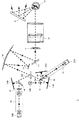
図1は、本実施形態の画像表示装置1の構成の一例を示す図である。画像表示装置1は、例えば、GLVからなる複数の変調素子を用いたプロジェクターである。
図1に示すように、画像表示装置1は光学系システム1aと信号処理部9と電源90とによって構成される。
光学系システム1aは、光源部2と、照明光学系3と、光変調部4と、空間フィルタ5(SFT)と、光投射部6と、スクリーン8とを有する。
信号処理部9は、映像信号入力処理部27(VSIP)と、素子駆動回路部28(DRV)と、システム制御部29(CPU)と、スキャン制御部30(SCMCNT)とを有する。
映像信号入力処理部27(VSIP)は、本発明の請求項における「初期駆動信号生成回路」に相当する。
素子駆動回路部28(DRV)は、本発明の請求項における「駆動回路」に相当する。
次に、以上の各部分の機能について簡単に説明し、そして、画像表示装置1において各構成成分の配置図2を用いて、各構成成分の構成と動作を詳細に説明する。
Hereinafter, embodiments of the present invention will be described with reference to the accompanying drawings.
First Embodiment FIG. 1 is a diagram illustrating an example of a configuration of an
As shown in FIG. 1, the
The optical system 1a includes a
The
The video signal input processing unit 27 (VSIP) corresponds to an “initial drive signal generation circuit” in the claims of the present invention.
The element driving circuit section (DRV) corresponds to a “driving circuit” in the claims of the present invention.
Next, the function of each part described above will be briefly described, and the configuration and operation of each component will be described in detail with reference to the layout diagram 2 of each component in the
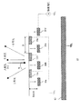
光源部2は、例えば、赤(R)、緑(G)、青色(B)レーザダイオードからなり、赤色、緑色、及び青色レーザビーム光を射出する赤色レーザ21R(LD(R))と、緑色レーザ21G(LD(G))と、青色レーザ21B(LD(B))とを含む。これらのレーザダイオードは電源90(PWR)から給電され、それぞれの色のレーザビームを射出する。
照明光学系3は、赤色用照明光学系22R(LG(R))と、緑色用照明光学系22G(LG(G))と、青色用照明光学系22B(LG(B))とを含み、1次元に配列されているGLVの形状に合わせて、赤色レーザ21Rと、緑色レーザ21Gと、青色レーザ21Bとから出射されたレーザ光の断面の形状を変形手段により変形し、収束レンズにより収束した後、変更ミラーによって光変調素子に集光する。
The
The illumination
光変調部4は、それぞれ1次元に羅列されてアレイ化され、1次元画像を表示する赤色用GLV(Grating Light Valve:回折格子ライト・バルブ)23R(GLV(R))と、緑色用GLV23G(GLV(G))と、青色用GLV23B(GLV(B))と、色合成部24(MX)とを含む。
各GLVは、例えば1080画素を表示する1080画素素子が1次元に配列してなり、画像信号に対応する駆動電圧の印加によって動作し、照明光学系3から射出されて、各GLVに入射した1次元方向に集光する照明光を反射又は回折し、反射光、又は、0次光、±1次光、±2次光等を含む回折光を射出する。即ち、各GLVは画像信号に応じてレーザビームを変調する変調手段として機能する。
色合成部24(MX)は、赤色用GLV23Rと、緑色用GLV23Gと、青色用GLV23Bとで変調された赤色、緑色、及び青色の変調光を色合成フィルターにより合成し、様々な色の変調光を生成し、カラー画像を表示する。ここで、色合成部を色合成手段とする。
The
Each GLV includes, for example, 1080 pixel elements displaying 1080 pixels arranged one-dimensionally, operates by applying a drive voltage corresponding to an image signal, and is emitted from the illumination
The color synthesizing unit 24 (MX) synthesizes red, green, and blue modulated lights modulated by the
空間フィルタ5(SFT)は、例えば、凹面および凸面ミラーを用いてGLVで生成された変調光のうち、強度が最も高く、画像表示に用いられる±1次回折光を選択し、光学系を通過させ、画像表示に用いない他の成分を遮断する。ここで、空間フィルターを表示分離手段とする。 For example, the spatial filter 5 (SFT) selects ± 1st-order diffracted light having the highest intensity and used for image display among modulated lights generated by the GLV using concave and convex mirrors, and passes through the optical system. Block other components not used for image display. Here, the spatial filter is a display separating unit.
光投射部6は、光拡散部(ディフューザ:diffuser)7(DIFF)と、投影レンズ25(PJL)と、スキャンミラー26(SCM)とを含む。
光拡散部7は、±1次回折光の断面を1次元方向に拡散し、線状の拡散光に変換する。投影レンズ25は、得られた1次元拡散光をスキャナーミラー26に投射する。スキャンミラー26は、例えばガルバノミラーからなり、映像信号に同期して回転し、1次元拡散光をスクリーン8上に投射しながら、所定の方向に走査し、スクリーン8上に投射表示画像を形成する。
The
The
信号処理部9において、映像信号入力処理部27では、例えば、DVDなどの映像再生機器より入力された映像信号VIDEOは、色差信号YCbCr(YPbPr)からRGB信号に変換される。非線形特性(γ特性)が付加されているので、映像信号入力処理部27では、逆ガンマ補正処理で線形特性に変換した後に、照明光源の色再現範囲に対応させるために、色空間変換処理を実施する。そして、その処理された映像信号を素子駆動回路部28に入力する。
素子駆動回路部28は、映像信号入力処理部27から出力された信号を受け、所定のタイミングでGLV23R、GLV23G、GLV23Bに印加し、GLV23R、GLV23G、GLV23Bを駆動して、赤色レーザ21R、緑色レーザ21G、青色レーザ21Bから出射されたレーザ光を変調する。
スキャン制御部30は、スキャンミラー26の回転を駆動及び制御する信号をスキャンミラー26に出力する。
CPU29は、映像信号入力処理部27(VSIP)と、素子駆動回路部28(DRV)と、スキャン制御部30(SCMCNT)を制御し、素子駆動回路部28からGLV23R、GLV23G、GLV23Bに印加する駆動電圧信号と、スキャン制御部30(SCMCNT)の出力信号と、及びGLV23R、GLV23G、GLV23Bの動作タイミング並びにスキャンミラー26の回転タイミングとを同期させる。
In the
The element
The
The
従って、画像表示装置1は、次のように動作して2次元カラー画像を表示する。
R,G,Bの各光源21Rと、21Gと、21Bとから出射された三原色の光が照明光学系3でそれぞれ1次元方向に集光され、各色用のGLV23Rと、23Gと、23Bとに照射される。各色用のGLVにおける各画素素子は、素子駆動回路部28から印加された駆動信号に応じて入射光の回折状態を制御し、各色の照明光を変調する。
変調されたR,G,Bの変調光は、色合成部24によって集光され、所望色の変調光を合成する。
その後、空間フィルタ5で不要な変調光(±1次回折光以外)を取り除き、光拡散部7にて変調光は拡散光に変換される。得られた1次元変調拡散光は投影レンズ25を通過し、スキャンミラー26に入射される。スキャン制御部30から入力される回転駆動信号に従って、スキャンミラー26は映像信号VIDEO並びに素子駆動回路部28から各GLVに印加した駆動信号に同期して、スクリーン8上に1次元変調拡散光を走査し、スクリーン8上に2次元カラー画像が形成される。
Therefore, the
The three primary colors of light emitted from the R, G, and B
The modulated R, G, and B modulated lights are condensed by the
Thereafter, unnecessary modulated light (other than ± first-order diffracted light) is removed by the spatial filter 5, and the modulated light is converted into diffused light by the
図2は、画像表示装置1における前述した各構成成分の配置の一例を示す図である。
図2に示すように、画像表示装置1において、緑色レーザ21Gと青色レーザ21Bは、紙面に平行する方向にレーザ光を射出するように配置されているのに対して、赤色レーザ21Rは赤色レーザ光が紙面と直交するように配置されている。
FIG. 2 is a diagram illustrating an example of the arrangement of the above-described components in the
As shown in FIG. 2, in the
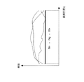
次に、図3〜図5を参照して、画像表示装置1の中核となる1次元画像素子GLV23R、23G、23Bの構成と動作原理を説明する。記載の便宜上、必要な場合にGLV23R、23G、23Bをまとめて符号23で表わす。
図3は、1次元画像を表示する1次元GLV23の部分模式的斜視図である。
図3に示すように、GLV23において、シリコン基板上のポリシリコン薄膜からなる共通電極12の上に、共通電極12と所定の間隔を保って、条帯状(ストリップ)のリボン電極10a,11a,10b,11b,10c,11c,10dが形成されている。これらのリボン電極は、上面に反射膜(不図示)が形成されており、反射部材として作用する。
Next, the configuration and operation principle of the one-dimensional image elements GLV23R, 23G, and 23B, which are the core of the
FIG. 3 is a partial schematic perspective view of the one-
As shown in FIG. 3, in the
図3に示すように、リボン電極10a,10b,10c,10dに駆動電圧を印加された時に、リボン電極10a,10b,10c,10dと共通電極12の間に静電力が生じ、その静電力により、リボン電極10a,10b,10c,10dは駆動電圧に応じて、図3において上下方向に移動または変形し、リボン電極10a,10b,10c,10dの反射膜の高さが変化する。一方、リボン電極11a,11b,11cは位置を一定とし、移動しない。
移動又は変形可能なリボン電極10a,10b,10c,10dは可動リボン電極、移動しないリボン電極11a,11b,11cは固定リボン電極と呼ぶ。
As shown in FIG. 3, when a driving voltage is applied to the
The movable or
リボン電極の代表的な寸法として、例えば、リボン電極の幅は3〜4μm、隣接するリボン電極間ギャップは約0.6μm、リボン電極の長さは200〜400μm程度である。
複数のリボン電極が1セットで1つの画素(ピクセル)に用いることができる。例えば、図3に示された隣接する6本のリボン電極10a,11a,10b,11b,10c,11cが1つの画素を表わすように用いることができる。この場合、1画素分の幅は約25μmである。
例えば、実用化されつつある1080画素を表示するGLVにおいては、図3の横方向に沿って、1080画素分のリボン電極が多数配置している。
As typical dimensions of the ribbon electrode, for example, the width of the ribbon electrode is 3 to 4 μm, the gap between adjacent ribbon electrodes is about 0.6 μm, and the length of the ribbon electrode is about 200 to 400 μm.
A plurality of ribbon electrodes can be used for one pixel in one set. For example, the six
For example, in a GLV displaying 1080 pixels, which is being put to practical use, a large number of ribbon electrodes for 1080 pixels are arranged along the horizontal direction in FIG.
図4と図5は、GLV23の動作原理を説明する。
図4と図5は、図3に示すGLV23の横方向の断面図である。図4において、可動リボン電極10a,10b,10c,10dへの駆動電圧がOFF、固定リボン電極11a,11b,11cが接地されている。この状態はGLV23のOFF状態という。
駆動電圧はゼロであるので、可動リボン電極10a,10b,10c,10dが移動せず、すべてのリボン電極が共通電極12から一定の距離を保ち、同じ平面に位置する。
4 and 5 illustrate the operation principle of the
4 and 5 are cross-sectional views of the
Since the driving voltage is zero, the
この状態で照明光をリボン電極に入射すると、各リボン電極10a,11a,10b,11b,10c,11c,10dにおいて反射された各反射光の全光路差は生じずに、0次(通常の反射方向)、±2次光など偶数次数の回折光のみが生じる。
画像表示装置1において、±1次回折光のみスクリーン8上に集光する構成であるため、上述のGLV23のOFF状態では、スクリーン8が黒になる。
When the illumination light is incident on the ribbon electrode in this state, the reflected light reflected by each of the
In the
図5においては、可動リボン電極10a,10b,10c,10dに所定の駆動電圧が印加され、固定リボン電極11a,11b,11cは接地されている。
図5に示すように、駆動電圧が印加された可動リボン電極10a,10b,10c,10dが、静電力で共通電極12側に引き下げられる。
例えば、波長λが532nmである入射光に対して、印加された駆動電圧に応じて、可動リボン電極10a,10b,10c,10dがλ/4引き下げられた場合は、可動リボン電極はλ/4=133nm移動する。可動リボン電極の移動量はλ/4となるときは、1次光の回折効率が最大となる。
In FIG. 5, a predetermined drive voltage is applied to the
As shown in FIG. 5, the
For example, when the
この状態では照明光をリボン電極に入射すると、可動リボン電極10a,10b,10c,10dで反射される光束と固定リボン電極11a,11b,11cで反射される光束間の全光路差は半波長λ/2となる。これにより、GLV23が反射型回折格子として機能し、反射光束(0次光)同士は干渉して打ち消し合い、±1次光、±3次光など奇数次数を含む回折光が生じる。
GLV23R、23G、23Bで生成された各次数の回折光は、GLV23R、GLV23G、GLV23Bの空間周期により決められた各方向に進行し、即ち、空間的に変調される。これらの回折光は色合成フィルタ24aと24bからなる色合成部24で合成され、所望の色の光束を生成し、オフナーリレーミラー5aとシュリーレンフィルタ5bからなる空間フィルタ5では、±1次光以外の回折光は取り除かれる。残りの±1次光は光拡散部7(ディフューザ)で拡散され、投影レンズ25にてスキャンミラー26に投影される。スキャンミラー26は、回折光をスクリーン8上に偏向して1次元画像を形成し、また、画像信号に応じて回転しているスキャンミラー26は回折光及び1次元画像をスクリーン8上に走査し、カラー画像を形成する。
In this state, when illumination light is incident on the ribbon electrode, the total optical path difference between the light beam reflected by the
The diffracted light of each order generated by the
続いて、図2に示された画像表示装置1の他の構成成分について説明する。
前述したように、赤色用照明光学系22Rと、緑色用照明光学系22Gと、青色用照明光学系22Bとからなる照明光学系3は、1次元画像素子であるGLV23R,23G,23Bの形状に合わせて、赤色レーザ21R、緑色レーザ21G、青色レーザ21Bからの光ビームの断面の形状を変換して、GLV23R、23G、23Bに照射する。
図2に示すように、赤色用照明光学系22Rは、ラインジェネレータ・エキズパンダ45、緑色用照明光学系22Gは、ラインジェネレータ・エキズパンダ46と、ミラー48と、収束レンズ49と、青色用照明光学系22Bは、ラインジェネレータ・エキズパンダ41と、収束レンズ43と、ミラー44とをそれぞれ含む。
各ラインジェネレータ・エキズパンダ(Line Generator Expander)は、2つの光学レンズからなり、線状に配列されたGLV23R,23G,23Bに照射する線状のレーザ光を形成する。
Next, other components of the
As described above, the illumination
As shown in FIG. 2, the red illumination
Each line generator / expander (Line Generator Expander) is composed of two optical lenses, and forms a linear laser beam to irradiate linearly arranged
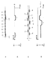
図6(a)、及び(b)と(c)は、各レーザ光源21R、21G、21Bから射出され、照明光学系22R、22G、22Bに入射する前のレーザビームの断面形状、及び空間強度分布を示す。図6(a)、(b)、及び(c)において、x軸は、いずれのGLVにおける各リボン電極と平行する方向となっており、即ち、図5に紙面と直交する方向である。y軸はいずれのGLVの長手方向となっており、即ち、リボン電極の羅列方向に沿って、各リボン電極と垂直している。図6(b)と(c)において、軸Iは光強度を表わす。
各レーザ光源21R、21G、21Bから射出されたレーザビームの断面形状は、例えば、図6(a)の実線で示されているように、スポットとなっている。図6(a)において、ビームの形状と比較するために、GLV23R、23G、23Bのいずれかの位置が破線で示されている。
図6(b)は、いずれのGLVにおいてリボン電極と平行する方向での照明光強度分布を示し、図6(c)は、いずれのGLVの長手方向での照明光強度分布を示す。
図6(a)〜(c)に示すように、各レーザ光源21R、21G、21Bから射出され、照明光学系3に成形されていないレーザビームは、GLV23R、23G、23Bのそれぞれの一部しか照射できず、照明光の強度分布は均一ではない。
FIGS. 6A, 6B, and 6C show cross-sectional shapes and spatial intensities of laser beams emitted from the respective
The cross-sectional shape of the laser beam emitted from each of the
FIG. 6B shows the illumination light intensity distribution in a direction parallel to the ribbon electrode in any GLV, and FIG. 6C shows the illumination light intensity distribution in any longitudinal direction of the GLV.
As shown in FIGS. 6A to 6C, laser beams emitted from the
図7(a)、及び(b)と(c)は、各レーザ光源21R、21G、21Bから射出され、照明光学系22R、22G、22Bに成形された後に出射されたレーザビームの断面形状、及び空間強度分布を示す。図7(a)、(b)、及び(c)において、x軸、y軸、及びI軸の定義は、図6と同様である。
図7(a)〜(c)に示すように、各レーザ光源21R、21G、21Bからのレーザビームは、照明光学系22R、22G、22Bに成形されて出射する。具体的に、レーザビームは、リボン電極方向においてリボン幅程度に収束され、GLVのリボン電極の羅列方向において、全リボン電極を照明するように成形される。したがって、照明光学系22R、22G、22Bから射出されたレーザビームの断面形状は、GLVの羅列方向に沿った線状になっており、GLVの全面に照射している。
GLVの各リボン電極はサイズが小さいので、照明光学系22R、22G、22Bの射出された光束は、x方向でのサイズが十分小さいものでなければならない。
FIGS. 7A, 7B, and 7C show cross-sectional shapes of laser beams emitted from the
As shown in FIGS. 7A to 7C, the laser beams from the respective
Since each ribbon electrode of the GLV is small in size, the luminous flux emitted from the illumination
図2に示すように、ラインジェネレータ・エキズパンダ41が射出された線状青色レーザビームは、収束レンズ43に収束され、ミラー44に偏向され、GLV23Bに集光される。ラインジェネレータ・エキズパンダ46が射出された線状緑色レーザビームは、ミラー48に偏向され、収束レンズ49に収束され、GLV23Gに集光される。ラインジェネレータ・エキズパンダ45が射出された線状赤色レーザビームは、図示しない収束レンズとミラーに収束、偏向され、GLV23Rに集光される。ここで、ラインジェネレータ・エキズパンダ41,45,46は、第1の成形手段とし、収束レンズ43,49は、第1の収束レンズとし、ミラー44,48は、第1の偏向ミラーとする。
As shown in FIG. 2, the linear blue laser beam emitted from the line generator /
空間変調器の機能を有するGLV23R、GLV23G、GLV23Bは、各画素素子の各リボン電極が印加された駆動電圧に応じて変位することにより、入射されたレーザ光を変調して、0次光、±2次光などの偶数次数の回折光、又は、±1次光、±3次光などの奇数次数の回折光を含む変調光を射出する。各次数の回折光は、GLV23R、GLV23G、GLV23Bの空間周期により決められた各方向に進行し、即ち、空間的に変調される。
射出された各色の変調光は、色合成部24で混合され、所望の色のレーザ光を形成する。
色合成部24は、第1の色合成フィルタ24aと、第2の色合成フィルタ24bとから構成されている。
The
The emitted modulated lights of each color are mixed in the
The
GLV23Rで変調された赤色のレーザ光と、GLV23Gで変調された緑色のレーザ光とが、第1の色合成フィルタ24aで先に色合成が行なわれる。
そして、GLV23Bで変調された青色のレーザ光が、第2の色合成フィルタ24bにおいて、第1の色合成フィルタ24aで合成されたレーザ光と合成される。
これで、3つのGLVで変調された3色の変調光は色合成が行なわれる。
青色レーザの輝度が緑色及び赤色に比べて低いため、青色と緑又は赤色とそのまま合成を行なうと、輝度の相違により、青色の成分が緑色又は赤色によって弱められる。赤色と緑色とは輝度が近似しているので、輝度レベルの調整を行なうことなく、色合成を行なうことができる。
The red laser light modulated by the
Then, the blue laser light modulated by the
Thus, the modulated light of the three colors modulated by the three GLVs is subjected to color synthesis.
Since the luminance of the blue laser is lower than that of green and red, if blue and green or red are directly synthesized, the blue component is weakened by green or red due to the difference in luminance. Since the luminances of red and green are similar, color synthesis can be performed without adjusting the luminance level.
図1に示された空間フィルタ5は、図2に示されたように、対向した位置に設けられている凹面のオフナーリレーミラー5aと凸面ミラーからなるシュリーレンフィルタ5bとから構成される。
図2に示すように、第2の色合成フィルタ24bで合成されたレーザ光は凹面のオフナーリレーミラー5aに照射され、凹面のオフナーリレーミラー5aは、その照射光を凸面のシュリーレンフィルタ5bに反射させる。
凸面ミラーからなるシュリーレンフィルタ5bは、凹面のオフナーリレーミラー5aのフーリエ面に配置され、凹面のオフナーリレーミラー5aとの曲率半径の比が1:2となっている。凹面のオフナーリレーミラー5aで反射された0次光、+2次光、−2次光、若しくは、+1次光、−1次光、並びに他の高次数の回折光は、シュリーレンフィルタ5bの凸面において、それぞれ異なる位置に収束する。シュリーレンフィルタ5bは、±1次光以外の回折光を取り除き、±1次光だけを光拡散部7に導く。
As shown in FIG. 2, the spatial filter 5 shown in FIG. 1 includes a concave Offner relay mirror 5a and a schlieren filter 5b composed of a convex mirror provided at opposing positions.
As shown in FIG. 2, the laser light synthesized by the second
The schlieren filter 5b composed of a convex mirror is arranged on the Fourier surface of the concave Offner relay mirror 5a, and has a radius of curvature ratio of 1: 2 with the concave Offner relay mirror 5a. The 0-order light, + 2nd-order light, -2nd-order light, + 1st-order light, -1st-order light, and other high-order diffracted lights reflected by the concave Offner relay mirror 5a are convex surfaces of the schlieren filter 5b. , Each converges to a different position. The schlieren filter 5b removes diffracted light other than the ± first-order light, and guides only the ± first-order light to the
図8(a)、(b)および(c)は、空間フィルタ5の原理を説明する模式図である。
図8(a)において、空間フィルター5は、オフナーリレーミラー5aの機能を表すレンズ51を示し、シュリーレンフィルタの機能を表す反射面52をそれぞれ有する。Xは、レンズ51のフーリエ面である。
レンズ51に照射された各次数の回折光は、フーリエ面Xに設けられた反射面52に収束する。例えば、0次光は位置bに収束し、+1次光と−1次光は、位置aと位置cにそれぞれ収束する。
図8(b)に示すように、反射面52において、位置aには開口部55が設けられており、0次光を通過させる。反射面52の位置aに対応する領域56a及び位置bに対応する領域56bは、+1次光と−1次光をそれぞれ反射させる。
±2次光、または、±3次光並びに他の高次数回折光は、反射面52において、位置aと位置cの両外側の位置、即ち、領域57aまたは57bに収束する。図8(b)に示すように、領域57aと57bには、開口部が設けられており、これらの高次数回折光を通過させる。
このように、シュリーレンフィルタ5bになる凸面反射面に、必要な回折光を反射させ、不必要な回折光を、その収束位置に開口部を設け、通過させることによって、空間フィルタ5は±1次光だけを取り出す。取り出された±1次光は、オフナーリレーミラー5aに反射される。空間フィルター5は、上記のように、表示光と非表示光とを分離する表示光分離手段とする。
FIGS. 8A, 8B and 8C are schematic diagrams illustrating the principle of the spatial filter 5. FIG.
In FIG. 8A, the spatial filter 5 shows a
The diffracted light of each order irradiated on the
As shown in FIG. 8B, an
The ± 2nd-order light, ± 3rd-order light, and other higher-order diffracted lights converge on the
As described above, the necessary diffraction light is reflected on the convex reflecting surface serving as the schlieren filter 5b, and the unnecessary diffraction light is provided with the opening at the convergence position and passed therethrough, so that the spatial filter 5 has ± 1 order. Take out only the light. The extracted ± 1st order light is reflected by the Offner relay mirror 5a. The spatial filter 5 is a display light separating unit that separates display light and non-display light as described above.
図2に示すように、凹面のオフナーリレーミラー5aは、第2の色合成フィルタ24bで合成されたレーザ光を、平板の反射ミラーより小さい反射角度で凸面のシュリーレンフィルタ5bに反射させる。凸面シュリーレンフィルタ5bは、±1次光を平板の反射ミラーより大きい反射角度でオフナーリレーミラー5aに反射させる。凹面のオフナーリレーミラー5aは、±1次光を平板の反射ミラーより小さい反射角度でミラーら50に反射させる。
凹面のオフナーリレーミラー5aと凸面のシュリーレンフィルタ5bの配置により、±1次光を無収差で取り出すことができる。
図8(c)は、図8(b)におけるZZ´方向に見た回折光の焦点位置を示す。図8(c)に示すように、各次数の回折光は、ZZ´方向に収束点が分離しているものの、ZZ´方向と直交する方向に、収束点は分離していない。
As shown in FIG. 2, the concave Offner relay mirror 5a reflects the laser beam synthesized by the second
Due to the arrangement of the concave Offner relay mirror 5a and the convex Schlieren filter 5b, ± first-order light can be extracted without aberration.
FIG. 8C shows the focal position of the diffracted light as viewed in the ZZ ′ direction in FIG. 8B. As shown in FIG. 8C, the converging points of the diffracted lights of the respective orders are separated in the ZZ ′ direction, but are not separated in the direction orthogonal to the ZZ ′ direction.
ミラー50は、変調光を光拡散部7に偏向する。光拡散部7は、図9(a)と(b)に図解したように、ミラー50から入射したレーザ光を、側面が幅の広い平行光(図9(a))、上面が幅の狭い平行光(図8(b))に拡散する。拡散された線状レーザ光は投射レンズ25に入射させる。投射レンズ25は、該拡散された線状レーザ光をスキャンミラー26に投射する。ここで、ミラー50は、第2の偏向ミラーとし、光拡散部7は、第2の成形手段とし、投射レンズ25は、投射光学系とする。
スキャンミラー26は、例えば、ガルバノミラーからなり、上記線状レーザ光を前方のスクリーン8に投射し、一列の画素からなる1次元画像を形成する。また、スキャンミラー26は画像信号に応じて回転しており、1次元画像をスクリーン8に走査し、2次元画像を形成する。さらに、スキャンミラー26は、走査手段とする。
The
The
本実施形態によれば、GLVを用いたプロジェクターである画像表示装置は、コンパクトにすることが可能である。また、質の良い表示色を合成でき、不必要な回折光を効率よく取り除き、画像表示に用いる回折光にノイズは少ないので、高品質のカラー映像を表示できる。 According to the present embodiment, the image display device which is a projector using the GLV can be made compact. In addition, high quality display colors can be synthesized, unnecessary diffracted light can be efficiently removed, and the diffracted light used for image display has little noise, so that a high-quality color image can be displayed.
第2の実施形態
本実施形態に係る画像表示装置は、基本構成が図1と図2で図解した第1の実施形態に係る画像表示装置と同様である。
レーザ光源21R、21G、21Bの照明条件の不均一性、及び1次元画像素子GLV23R、GLV23G、GLV23Bにおける各画素素子の変調特性にバラツキが存在するので、それらにより、表示される画像は色と輝度の不均一性が存在する。本実施形態は、その不均一性を検出して補正し、高画質の映像を表示可能な画像表示装置について述べる。
なお、本実施形態において、第1の実施形態の画像表示装置と同じ構成成分に同じ符号を用い、重複する説明を省略する。
Second Embodiment The image display device according to the present embodiment has the same basic configuration as the image display device according to the first embodiment illustrated in FIGS.
The unevenness of the illumination conditions of the
Note that, in the present embodiment, the same reference numerals are used for the same components as those of the image display device of the first embodiment, and overlapping descriptions will be omitted.
照明条件が均一で、かつGLV23R、GLV23G、GLV23Bにおける各画素素子の変調特性にバラツキが存在しない場合は、上記に説明した画像表示装置において、画像信号をGLV23R、GLV23G、GLV23Bの駆動回路に入力し、GLV23R、GLV23G,GLV23Bを動作することによって、理想的な映像を表示できる。
しかし、実際に、GLV23R、GLV23G、GLV23B自体の特性や駆動回路特性にバラツキが存在する。そのため入射光に対して均一にならず、画面上に横縞が発生し、輝度の不均一性が生じる。
また、照明条件に関しては、照明光学系を最適化しても、GLV全体に亘って照明条件を均一することが困難であり、画面上に輝度と色表示の不均一性が生じる。
When the illumination conditions are uniform and there is no variation in the modulation characteristics of the pixel elements in the GLV23R, GLV23G, and GLV23B, an image signal is input to the drive circuits of the GLV23R, GLV23G, and GLV23B in the above-described image display device. , GLV23R, GLV23G, and GLV23B can be operated to display an ideal image.
However, actually, there are variations in the characteristics of the
Regarding the illumination conditions, even if the illumination optical system is optimized, it is difficult to make the illumination conditions uniform over the entire GLV, and unevenness in luminance and color display occurs on the screen.
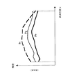
図10は、図3に示すGLV23の横方向の断面図である。
図10(a)と(c)において、6本のリボン電極10a,11a,10b,11b,10c、並びに11cはGLV23の1画素素子を構成する。隣接するリボン電極10d,11d,10eは隣接する画素素子を構成するリボン電極である。図3〜図5と同じように、リボン電極10a,10b,10c,10d,10eが可動リボン電極、リボン電極11a,11b,11c,11dは固定リボン電極である。
図10(b)および図10(d)は、図10(a)および図10(c)に示すGLVの動作状態に対応するスクリーン8上に形成された1次元画像の輝度分布を示す図である。
FIG. 10 is a lateral cross-sectional view of the
10A and 10C, six
FIGS. 10B and 10D are diagrams showing the luminance distribution of the one-dimensional image formed on the screen 8 corresponding to the operation state of the GLV shown in FIGS. 10A and 10C. is there.
図10(a)は、駆動電圧が印加されていない時に、GLVにおける各リボン電極の位置のバラツキを例示する図である。図10(b)は、可動リボン電極に駆動電圧が印加されていない時に、図10(a)の状態のGLVに対応するスクリーン8上に1次元画像の輝度分布を示す図である。
図10(a)に示すように、駆動電圧が印加されていなくても、リボン電極10aと10dは、他のリボン電極と同じ平面に位置せず、それぞれΔD1、ΔD2の高低差がある。これにより、GLVの各画素素子の変調特性に固有のバラツキが存在する。
駆動電圧が印加されていない場合は、照明光をGLV23に入射した時、理想的には、回折光が発生せず、スクリーン8上に黒が表示される。しかし、GLVのリボン電極の高低差により、僅かな回折光が発生し、スクリ−ン8の暗画面に、リボン電極10aと10dに対応する位置iとjに意図しない明るいスポットが表示される。さらに、スキャンミラー26は該1次元画像を走査し、スクリーン8上に横縞が形成され、画面のコントラストが低下する。
FIG. 10A is a diagram illustrating a variation in the position of each ribbon electrode in the GLV when a drive voltage is not applied. FIG. 10B is a diagram illustrating a luminance distribution of a one-dimensional image on the screen 8 corresponding to the GLV in the state of FIG. 10A when a driving voltage is not applied to the movable ribbon electrode.
As shown in FIG. 10A, even when the drive voltage is not applied, the
When the driving voltage is not applied, when the illumination light enters the
図10(c)は、駆動電圧が印加された時に、GLVにおける各リボン電極の位置のバラツキを例示する図である。図10(d)は、図10(c)に示す状態のGLVに対応するスクリーン8上に1次元画像の輝度分布を示す図である。
図10(c)に示すように、駆動電圧が印加された時は、リボン電極10cと10dは、意図せぬ位置に移動し、所望の位置とそれぞれΔZ1、−ΔZ2の高低差がある。スクリーン8上において、リボン電極10c,10dに対応する位置kとlで輝度は、所望の輝度と一致せず、輝度のバラツキが生じる。同じように、スキャンミラー26は該1次元画像を走査し、スクリーン8上に横縞を形成してしまい、画質を劣化させる。
FIG. 10C is a diagram illustrating a variation in the position of each ribbon electrode in the GLV when a driving voltage is applied. FIG. 10D is a diagram showing a luminance distribution of a one-dimensional image on the screen 8 corresponding to the GLV in the state shown in FIG. 10C.
As shown in FIG. 10C, when the driving voltage is applied, the
図11は、赤色(R)、緑色(G)、青色(B)のレーザ21R、21G、21Bに存在する照明条件の不均一性により、スクリーン8上の1次元画像における色と輝度の不均一性を例示する図である。GLV23R、23G、23Bの各々に照明条件が不均一であるので、画面上に輝度と色表示の不均一性が生じ、スキャンミラーの走査により、色と輝度の横縞が生じる。
FIG. 11 shows non-uniformity of color and brightness in a one-dimensional image on the screen 8 due to non-uniformity of illumination conditions existing in the red (R), green (G), and blue (B)
このような画像素子と光源に固有な特性のバラツキや不安定による画面上の輝度と色の不均一性を解消するために、本実施形態において、光検出装置及び補正の演算を行なう回路とを設けて、その輝度と色の不均一性を予め測定して補正し、得られる最適化の結果をデータテーブルとしてメモリに記憶し、画像表示の際に用いる。 In order to eliminate the non-uniformity of the luminance and color on the screen due to the variation and instability of the characteristics inherent to the image element and the light source, in the present embodiment, the light detecting device and the circuit for performing the calculation of the correction are used. The non-uniformity of the brightness and the color is measured and corrected in advance, and the obtained optimization result is stored in a memory as a data table and used for displaying an image.
図12は、本実施形態の画像表示装置101の構成の一例を示す図である。
図13は、画像表示装置101における前述した各構成成分の配置の一例を示す図である。
図13に示すように、画像表示装置101において、光学系システム101aでは、光源部2と、照明光学系3と、光変調部4と、空間フィルタ5(SFT)と、光投射部6と、スクリーン8とに加えて、光検出装置15が設けられている。
また、図12に示すように、信号処理部9において、映像信号入力処理部27(VSIP)と、素子駆動回路部28(DRV)と、システム制御部29(CPU)と、スキャン制御部30(SCMCNT)とに加えて、表示される色と輝度の不均一性を検出するためにGLV23R、GLV23G、GLV23Bにそれぞれテスト駆動電圧を印加するテスト信号生成部31と、光検出装置15で検出した信号を処理する検出信号処理部32(DSP)と、検出信号に基づいて、表示される色と輝度の不均一性を補正する最適な駆動電圧を求める補正回路部33が設けられている。
映像信号入力処理部27(VSIP)は、本発明の請求項における「初期駆動信号生成回路」に相当する。
素子駆動回路部28(DRV)は、本発明の請求項における「駆動回路」に相当する。
テスト信号生成部31と、検出信号処理部32(DSP)と、補正回路部33とは、本発明の請求項における「補正手段」に相当する。
FIG. 12 is a diagram illustrating an example of the configuration of the
FIG. 13 is a diagram illustrating an example of the arrangement of the above-described components in the
As shown in FIG. 13, in the
12, in the
The video signal input processing unit 27 (VSIP) corresponds to an “initial drive signal generation circuit” in the claims of the present invention.
The element driving circuit section (DRV) corresponds to a “driving circuit” in the claims of the present invention.
The test
光検出装置15は、本実施形態においてGLVの各画素素子から射出された変調光を測定し、変調特性を求める。また、変調特性のバラツキ及び照明条件により表示された輝度と色の不均一性を検出する。図12に示すように、光検出装置15は、反射ミラー16と、例えば、積分球、或は、CCD等からなる光センサ17とを含む。さらに、図13に示すように、反射ミラー16と光センサ17の間に偏向されたレーザ光を収束するレンズ18が設けられている。
反射ミラー16は、投影レンズ25から射出された変調光を光センサ17に偏向する。
光センサ17は、例えば、積分球を用いる場合は、入力した光を外部に漏出させないように積分球内部で反射し、入射された光の全てを集め、そのエネルギー、即ち、入射された光の光量を測定する。
反射ミラー16は、例えば、表示不均一性を予め測定する時のみ図13に示す位置に設置し、光路を変更する。実際に画像を表示する時に、反射ミラー16を外し、通常の光路になる。
光検出装置15は、本発明の請求項における「測定手段」に相当する。
The
The
For example, when an integrating sphere is used, the
For example, the
The light detecting
従って、画像表示装置101は、次のように動作して2次元カラー画像を表示する。
まず、予め表示される輝度と色の不均一性を測定して補正する。
図14はその流れを示すフローチャートである。
ステップS11:
画像表示装置101における表示輝度と色の不均一性の測定を行なう。
ステップS12:
レーザ光源21R、21G、21Bは、GLV23R、GLV23G、GLV23Bに順次照射し、各GLVの各画素素子について、テスト信号生成部31が例えば所定の最小電圧から所定の最大電圧値までのテスト信号を駆動信号として照射されたGLVにおける全ての画素素子に印加する。光検出装置15が個々の画素素子から射出された変調光の光量を個別に測定する。
Therefore, the
First, non-uniformity of luminance and color displayed in advance is measured and corrected.
FIG. 14 is a flowchart showing the flow.
Step S11:
The display luminance and the color non-uniformity in the
Step S12:
The
ステップS13:
検出信号処理部32は、光検出装置15で測定された各画素素子からの変調光の信号について、ゲインの調整、A/D変換などの初期処理を施す。補正回路部33は、光検出装置15で測定された各画素素子からの変調光の光量を用いて、各画素素子による画像表示の輝度と色の不均一性を解析して検出し、所定の初期駆動電圧に対して、各色の各画素素子に印加する最適な駆動電圧を求める。求められた最適化した駆動電圧データのデータテーブルを作成し、表示装置101のメモリに記憶する。
実際に画像を表示する際に、記憶された駆動電圧のデータテーブルを用いて、GLVの各画素素子に印加する。
その後の画像表示の流れは、第1の実施形態と同様である。
Step S13:
The detection
When an image is actually displayed, the driving voltage is applied to each pixel element of the GLV using a stored data table of the driving voltage.
The subsequent image display flow is the same as in the first embodiment.
次に、本実施形態において、表示される輝度と色の不均一性を測定と補正する方法を説明する。
図15は、信号処理部9の詳細な構成を示すブロック図である。
図15において、映像信号入力処理部27は、逆γ補正回路69(IGC)と色空間変換回路70(CSC)を有し、例えば色差信号YCbCr(YPbPr)から変換されたRGB信号である映像信号VIDEOを処理する。
逆γ補正回路69は、RGB信号に付加されている非線形特性(γ特性)を、逆ガンマ補正処理で線形特性に変換する。
色空間変換回路70は、照明光源の色再現範囲に対応させるために、RGB信号について、色空間変換処理を実施する。このように処理された映像信号VIDEO補正回路部33に入力する。
Next, a method for measuring and correcting non-uniformity of displayed luminance and color in the present embodiment will be described.
FIG. 15 is a block diagram illustrating a detailed configuration of the
In FIG. 15, the video signal
The inverse
The color
検出信号処理部32は、ゲイン調整回路61(GM)とA/D変換回路62とを有し、光センサ17で測定された各画素素子からの変調光の信号について初期処理を施す。
ゲイン調整回路61は、検出された変調光信号について、レーザ光源21R、21G、21Bから射出された、異なる波長のレーザ光に対して、光センサ17における検出感度の相違を補正する。
A/D変換回路62は、該補正した後の検出信号をディジタル信号に変換する。変換された検出データは、補正回路部33内のメモリ63に順次蓄積される。
The detection
The
The A /
補正回路部33は、メモリ63と、補正値演算器64(CCAL)と、データテーブル記憶部65(LUT)と、選択回路66(SEL)とを有する。
GLV23R,GLV23G,GLV23Bにおける全ての画素素子について変調光の測定を行ない、得られたデータをメモリ63に蓄積する。その後、補正値演算器64は、各画素素子の測定データを用いて、各画素素子の変調特性を求め、各GLVの照明プロファイルを導出する。GLVごとの各画素素子について、所定の初期駆動電圧に対して、各GLVの照明プロファイルにおける輝度と色の不均一性がなくなるように、各GLVの各画素素子に印加する最適な駆動電圧を求める。求められた最適化された駆動電圧データのデータテーブルを作成し、データテーブル記憶部65に記憶する。
The
The modulation light is measured for all the pixel elements in the GLV23R, GLV23G, and GLV23B, and the obtained data is stored in the memory 63. Thereafter, the
画像を表示する時に、データテーブル記憶部65に記憶された補正後の駆動信号を素子駆動回路部28に出力し、画像表示を行なう。
選択回路66は、表示前に表示不均一性を測定及び補正する時に、テスト信号生成部31から出力するテスト駆動信号と、画像を表示する時にデータテーブル記憶部65に記憶された補正後の駆動信号とを切り替え、必要な方を選択する。
補正値演算器64における処理について、後程詳細に述べる。
When displaying an image, the corrected drive signal stored in the data
The selection circuit 66 measures the test drive signal output from the test
The processing in the
素子駆動回路部28は、D/A変換回路67と、駆動回路68(DRVC)を有する。D/A変換回路67は、補正回路部33から出力されたディジタル駆動信号をアナログ信号に変換する。駆動回路68は、そのアナログ信号をGLV23R、GLV23G、GLV23Bの所定の画素素子の各リボン電極に印加する。GLV23R、GLV23G、GLV23Bは駆動信号に応じて動作し、赤色レーザ21R、緑色レーザ21G、青色レーザ21Bから出射されたレーザ光を変調する。
CPU29は、信号処理部9の上記各構成成分の動作タイミングを制御する。
The element
The
次に、図14におけるステップS12、即ち、表示される輝度と色の不均一性を検出する方法を説明する。
図16は、表示される輝度と色の不均一性を測定する処理を説明するフローチャートである。
ステップS21:
画像表示を行なう前に、ミラー16と光センサ17を設置し、輝度と色の不均一性を予め測定する。
ステップS22:
レーザ光源、例えば、赤色レーザ光源21Rを点灯し、射出されたレーザ光は照明光学系22Rで線形に成形され、GLV23R全体に照射する。
Next, step S12 in FIG. 14, that is, a method of detecting nonuniformity of displayed luminance and color will be described.
FIG. 16 is a flowchart illustrating a process for measuring the nonuniformity of the displayed luminance and color.
Step S21:
Before displaying an image, a
Step S22:
The laser light source, for example, the red laser
ステップS23:
GLV23Rの全ての画素素子の変調特性、即ち、駆動電圧と変調光の輝度の関係を順次測定する。
ある画素素子の変調特性を測定するために、テスト信号生成部31で生成したテスト信号を、駆動電圧信号として選択回路66を介して測定対象画素素子の駆動回路に入力し、該測定対象画素素子の各リボン電極に印加する。
Step S23:
The modulation characteristics of all the pixel elements of the
In order to measure the modulation characteristic of a certain pixel element, the test signal generated by the test
図17(a)は、テスト信号生成部31が生成したテスト信号の波形を示す。
テスト信号生成部31が生成したテスト信号は、図17(a)に示すように、時間につれて、信号のレベル(相対値)は0、1、…、254、255というように徐々に変化する、いわゆる三角信号である。
測定対象画素素子は、図17(a)に示された、レベル(相対値)が0、1、…、254、255というように変化する駆動信号に応じて駆動し、入射された赤色レーザ光を変調し、それぞれのレベルに応じた強度の回折光からなる変調光を射出する。
図17(a)に示したテスト信号は、本発明の請求項における「第1のテスト信号」に相当する。信号レベルの最小(0)から最大(255)までの変化範囲は本発明の請求項における「第1の変化範囲」に相当する。
レーザ光源21はGLV23R全体に照射する場合に、該光源21は本発明の請求項における「第1の照明手段」に相当する。
FIG. 17A shows the waveform of the test signal generated by the
In the test signal generated by the test
The pixel element to be measured is driven according to the drive signal whose level (relative value) changes as 0, 1,..., 254, 255 shown in FIG. And emits modulated light composed of diffracted light having an intensity corresponding to each level.
The test signal shown in FIG. 17A corresponds to the “first test signal” in the claims of the present invention. The change range of the signal level from the minimum (0) to the maximum (255) corresponds to the “first change range” in the claims of the present invention.
When the laser light source 21 irradiates the
光センサ17は、入射される変調光の強度を測定し、測定された変調光の強度を電気信号に変換して出力する。
変調光の強度は、GLV23Rにおける1画素当たりのリボン電極間の段差による。該段差はリボン電極の固有の表面位置のバラツキと、駆動電圧の精度によるリボン電極の表面位置のバラツキに起因する。
図17(b)は、印加されたテスト信号の各レベルに対する、光センサ17が測定した変調光の強度に相当する出力信号のレベル、いわゆる変調特性である。
図17(b)に示すように、テスト信号の電圧値が線形的に変化するのに対して、変調光の強度の変化は線形ではない。駆動電圧のレベルは小さい場合は、変調光の強度はゼロであり、駆動電圧のレベルがある値を越えると、変調光の強度は急に増大する。
The
The intensity of the modulated light depends on the level difference between the ribbon electrodes per pixel in the
FIG. 17B shows a level of an output signal corresponding to the intensity of the modulated light measured by the
As shown in FIG. 17B, while the voltage value of the test signal changes linearly, the change in the intensity of the modulated light is not linear. When the driving voltage level is small, the intensity of the modulated light is zero, and when the driving voltage level exceeds a certain value, the intensity of the modulated light sharply increases.
図18は、光センサ17の感度の波長による変化を示す図である。図18に示すように、光センサ17は、異なる波長の光に対して、測定感度が異なる。即ち、強度が同一、波長が異なる入射光に対して、光センサ17の出力のレベルが変化する。従って、R,G,B三色のレーザ光について、各GLVの各画素素子の変調特性を測定する場合、測定結果を規格化する必要がある。
センサの波長感度差を補正するため、センサの波長感度を事前に測定し、レーザ光源21R、21G、21Bから射出する光の波長の場合の規格係数fr、fg、fbを求めておく。そして、レーザ光源21R、21G、21Bを点灯する場合の光センサ17の出力に対して、係数fr、fg、fbをそれぞれ掛け、光源毎の光センサ17のゲインを合わせる。
これによって、ある画素素子に所定の駆動電圧を印加し、該画素素子には同じ強度のR,G,B三色の照明光を照射する場合は、光センサ17の出力(電圧値)が同じになる。
FIG. 18 is a diagram illustrating a change in the sensitivity of the
In order to correct the difference in the wavelength sensitivity of the sensor, the wavelength sensitivity of the sensor is measured in advance, and the standard coefficients fr, fg, and fb for the wavelength of the light emitted from the
Thus, when a predetermined drive voltage is applied to a certain pixel element and the pixel elements are irradiated with three colors of R, G, and B illumination light having the same intensity, the output (voltage value) of the
図15に示された検出信号処理部32におけるゲイン調整回路61は、上記したゲイン合わせの処理を行なう。
A/D変換回路62は、ゲイン調整回路61から出力されたアナログ信号をデジタルデータに変換し、256個のデータを補正回路部33のメモリ63に記憶する。該256個のデータは測定対象画素素子の変調特性となる。
図17(b)に示す結果は、1画素素子の変調特性の測定結果である。GLV23Rは、例えば、1080画素を表示する場合、以上の測定を1080回繰り返し、GLV23Rの1080画素素子について、同じように変調特性を測定し、得られた1080×256のデータをメモリ63に記憶する。
所定の1画素素子について測定を行なう場合、照明光を照射されないように、他の画素素子を遮光する。
The
The A /
The result shown in FIG. 17B is a measurement result of the modulation characteristic of one pixel element. For example, when displaying 1080 pixels, the
When the measurement is performed for a predetermined one pixel element, the other pixel elements are shielded so as not to be irradiated with the illumination light.
ステップS24:
例えば、GLV23Rの全ての画素素子の変調特性を測定した後に、レーザ光源21Rを消灯する。
ステップS25:
レーザ光源21G、または、21Bについても、同じように処理を行ない、GLV23G,または、GLV23Bの全部の画素素子の変調特性を測定する。
測定されたGLV23G,GLV23Bの全部の画素素子の変調特性のデータもメモリ63に記憶される。
GLV23R,GLV23G,GLV23Bのそれぞれの全部の画素素子の変調特性データを、まとめて関数Ir(v、x)、Ig(v、x)、Ib(v、x)で表す。ここで、変数vは、駆動電圧を表し、変数xは、各画素素子の位置を表し、画素素子を区別する変数である。r、g、bは、赤、緑、青三色を表す。
Step S24:
For example, after measuring the modulation characteristics of all the pixel elements of the
Step S25:
The same processing is performed for the
The data of the modulation characteristics of all the pixel elements of the measured
The modulation characteristic data of all the pixel elements of the GLV23R, GLV23G, and GLV23B are collectively represented by functions Ir (v, x), Ig (v, x), and Ib (v, x). Here, the variable v represents the drive voltage, the variable x represents the position of each pixel element, and is a variable for distinguishing the pixel element. r, g, and b represent three colors of red, green, and blue.
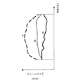
図19は、テスト信号のあるレベルv1で、GLV23R,23G,23Bの変調特性Ir(v1、x)、Ig(v1、x)、Ib(v1、x)の一例を示し、各GLVにおいて、各画素素子から射出された変調光の強度の変動を例示する。
図19に示すように、GLV23R,23G,23Bの画素素子の配置方向に沿って、変調光の強度が大きく変動する。
GLV23R,23G,23Bから射出された変調光の強度は、各画素素子の各リボン電極の位置のバラツキ、及び、レーザ光源21R、21G,21Bの強度による。特に、各レーザ光源は各GLVの全画素に渡って照射光の強度は変動しており、均一ではない。さらに、この照明光の強度分布は経時変化や温度変化をする。
FIG. 19 shows an example of the modulation characteristics Ir (v1, x), Ig (v1, x), and Ib (v1, x) of the
As shown in FIG. 19, the intensity of the modulated light greatly fluctuates along the arrangement direction of the pixel elements of the
The intensity of the modulated light emitted from the
メモリ63に記憶されたGLV23R,GLV23G,GLV23Bの全ての画素素子の変調特性データは、補正回路部33に含まれる補正値演算器64において解析されて、表示される輝度と色の不均一性を解消する。
図20は補正値演算器64の構成を示す。
補正値演算器64は、GLV23R,23G,23Bの変調特性Ir(v、x)、Ig(v、x)、Ib(v、x)の値を電圧値から輝度値IYr(v、x)、IYg(v、x)、IYb(v、x)に変換する電圧/輝度変換部81(L/V)と、上記輝度関数IYr(v、x)、IYg(v、x)、IYb(v、x)を解析する輝度分布解析部82(LDA)と、所望の変調特性関数を生成する理想変調特性関数生成部83(IV0)と、乗算器84と、駆動信号の補正を行ない、補正データテーブルを生成する補正テーブル生成部85a、85b、85c(CTG)と、駆動信号の補正データテーブルを書き込むデータテーブル記憶部86a、86b、86cと(LUT_R,LUT_G,LUT_B)を有する。
The modulation characteristic data of all the pixel elements of the GLV23R, GLV23G, and GLV23B stored in the memory 63 is analyzed by the
FIG. 20 shows the configuration of the
The
次に、図21のフローチャートを参照しながら、補正値演算器64の動作を説明する。
ステップS31:
R,G,Bレーザ光源について、GLV23R,23G,23Bそれぞれの全画素の変調特性Ir(v,x)、Ig(v,x)、Ib(v,x)を測定し、メモリ63に記憶する。その後に、補正回路部33において、その測定データを処理し、補正を行なう。
Next, the operation of the
Step S31:
For the R, G, B laser light sources, the modulation characteristics Ir (v, x), Ig (v, x), Ib (v, x) of all the pixels of the
ステップS32:
測定されたGLV23R,23G,23Bの変調特性Ir(v,x)、Ig(v,x)、Ib(v,x)は電圧値であり、補正値演算器64に含まれる電圧/輝度変換部81は、それら電圧値を輝度に変換する。
Step S32:
The measured modulation characteristics Ir (v, x), Ig (v, x), and Ib (v, x) of the
具体的に、まずは、目標とする白色光を実現するために、R,G,B三原色の混合比Rc、Gc、Bcを求める。
たとえば、R,G,B3原色の各三刺激値をR(Xr、Yr、Xr)、G(Xg、Yg、Zg)、B(Xb、Yb、Zb)、白の三刺激値をW(Xw、Yw、Zw)とする。その結果、白色を実現ための三原色の混合量Rc,Gc,Bcと各三刺激値の関係は下記の式(1)で定義される。
Specifically, first, in order to achieve a target white light, the mixing ratios Rc, Gc, and Bc of the three primary colors R, G, and B are obtained.
For example, the tristimulus values of the three primary colors R, G, and B are R (Xr, Yr, Xr), G (Xg, Yg, Zg), B (Xb, Yb, Zb), and the tristimulus value of white is W (Xw , Yw, Zw). As a result, the relationship between the mixing amounts Rc, Gc, Bc of the three primary colors and the respective tristimulus values for realizing white is defined by the following equation (1).

本実施形態に用いるR,G,Bレーザ光源の三刺激値および、白(色温度6500K)の三刺激値は、例えば、下記のような値となる。
R(0.4121、 0.1596、 0.0000)、
G(0.1891、 0.8850、 0.0369)、
B(0.3089、 0.0526、 1.7209)、
W(0.9505、 1.0000, 1.0890)。
白を実現するためのR,G,B三原色の混合量は式(1)に上記値を代入することによって下記の式(2)のように求められる。
The tristimulus values of the R, G, and B laser light sources and the tristimulus values of white (color temperature 6500K) used in the present embodiment are, for example, as follows.
R (0.4121, 0.1596, 0.0000),
G (0.1891, 0.8850, 0.0369),
B (0.3089, 0.0526, 1.7209),
W (0.9505, 1.0000, 1.0890).
The mixing amount of the three primary colors R, G, and B for realizing white can be obtained as in the following equation (2) by substituting the above values into the equation (1).
上記混合量は、上記三刺激値を持つ3原色にて色温度6500Kの白を輝度Y=1で実現するために必要なレーザーパワーの比をあらわしている。即ち、Rc:Gc:Bc=1.4648:0.8292:0.6510。
光センサ17にて各色の変調光量[W]を測定した結果Ir(v,x),Ig(v,x),Ib(v,x)は、図19に示されたものである。
かかるGLVから射出される変調光を全部混合する場合に実現可能な白の輝度をYwr,Ywg,Ywbで表わし、下記の式(4)のように求められる。
The mixing amount represents the ratio of the laser power required to realize white with a color temperature of 6500 K at the luminance Y = 1 in the three primary colors having the above-mentioned tristimulus values. That is, Rc: Gc: Bc = 1.648: 0.8292: 0.6510.
As a result of measuring the modulated light amount [W] of each color by the
The white luminance achievable when all the modulated lights emitted from the GLV are mixed is represented by Ywr, Ywg, and Ywb, and is obtained as in the following equation (4).
〔数4〕
Ywr=Ir(v,x)/Rc
Ywg=Ig(v,x)/Gc
Ywb=Ib(v,x)/Bc
(4)
[Equation 4]
Ywr = Ir (v, x) / Rc
Ywg = Ig (v, x) / Gc
Ywb = Ib (v, x) / Bc
(4)
前述したように、光センサ17は図18に示すような波長感度を持っている。また、光センサ17は、幾何学条件により、測定効率は100%ではない。そのため、これらの効果を補正する必要がある。具体的には、予め光センサ17の受光面積や波長感度による測定量の変化を反映する輝度変換係数Kr,Kg,Kbを求め、上記輝度関数Ywr,Ywg,Ywbに掛け、補正する。
従って、補正後の実現可能な白色の輝度IYは次の式(5)のようになる。
〔数5〕
IYr=Kr×Ywr=Kr×I(v,x)/Rc(ルーメン)
IYg=Kg×Ywg=Kg×Ig(v,x)/Gc(ルーメン)
IYb=Kb×Ywb=Kb×Ib(v,x)/Bc(ルーメン)
(5)
As described above, the
Therefore, the achievable white luminance IY after the correction is as shown in the following equation (5).
[Equation 5]
IYr = Kr × Ywr = Kr × I (v, x) / Rc (lumen)
IYg = Kg × Ywg = Kg × Ig (v, x) / Gc (lumen)
IYb = Kb × Ywb = Kb × Ib (v, x) / Bc (lumen)
(5)
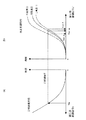
図22は、図19に示された駆動電圧v=v1の時の変調特性の分布(光量−画素位置)を電圧/輝度変換部81において上記のように処理することによって、得られた輝度特性(または、輝度プロファイル、即ち輝度と画素位置の関係)IYr,IYg,IYbを示す。
ステップS33:
輝度分布解析部82は、輝度特性(輝度−画素位置)IYr,IYg,IYbを解析し、各駆動電圧vに対して、IYr(v、x),IYg(v、x),IYb(v、x)の共通の最小値IY0を探し、その値を補正回路33で補正を行なった後に、実現可能な白の最大輝度IYmaxとする。
IY0より大きい白の輝度は、GLV23R,23G,23Bの中に、その輝度を実現できない画素素子は必ず存在するからである。
図22において、輝度特性IYr(v、x),IYg(v、x),IYb(v、x)の共通の最小値IY0は、IYb(v、x)の最小値となる。即ち、IYb(v、x)が白を実現する上で拘束条件になり、IYb(v、x)の最小値IY0が実現可能な白の最大輝度IYmaxになる。
FIG. 22 shows a luminance characteristic obtained by processing the distribution of the modulation characteristic (light quantity-pixel position) when the drive voltage v = v1 shown in FIG. (Or a luminance profile, that is, a relation between luminance and pixel position) IYr, IYg, and IYb.
Step S33:
The luminance distribution analysis unit 82 analyzes luminance characteristics (luminance-pixel position) IYr, IYg, IYb, and for each drive voltage v, IYr (v, x), IYg (v, x), IYb (v, The common minimum value IY0 of x) is searched, and the value is corrected by the
This is because there is always a pixel element in the
In FIG. 22, the common minimum value IY0 of the luminance characteristics IYr (v, x), IYg (v, x), and IYb (v, x) is the minimum value of IYb (v, x). That is, IYb (v, x) becomes a constraint condition for realizing white, and the minimum value IY0 of IYb (v, x) becomes the maximum achievable white luminance IYmax.
ステップS34:
前述したように、画像入力機器によって入力映像信号VIDEOが特有のγ特性を有する、即ち、入力信号をx(0<x<1)、出力信号をy(0<y<1)とすると、y=xγの関係が成立する。例えば、通常テレビの場合、γ=2.2である。
その結果、入力映像信号VIDEOのγ特性に応じて、GLV23R,23G,23Bの画素素子には、理想的な変調特性が存在する。ここで、GLV23R,23G,23Bの入力映像信号VIDEOのγ特性に応じた変調特性を関数IV(t)で表わし、全部画素素子の理想的な変調特性IT(v)は、変調特性IV(t)と、上記において求めた白の最大輝度IYmaxとの積になる。即ち、IT(v)=IYmax×IV(v)となる。以降、理想的な変調特性IT(v)を目標変調特性と呼ぶ。γに応じた変調特性IV(t)は、ユーザにより指定可能である。
補正値演算器64において、輝度分布解析部82は実現可能な白の最大輝度IYmaxを出力し、理想変調特性関数生成部83は、ユーザが指定した理想変調特性関数IV(t)を出力する。乗算器84において、関数IYmaxと関数IV(t)を乗算し、その乗算の結果は目標変調特性IT(v)となる。
図23は、このように求められた目標変調特性IT(v)の一例を示す。
Step S34:
As described above, the input video signal VIDEO has a specific γ characteristic depending on the image input device, that is, if the input signal is x (0 <x <1) and the output signal is y (0 <y <1), y = Xγ. For example, in the case of a normal television, γ = 2.2.
As a result, the pixel elements of the
In the
FIG. 23 shows an example of the target modulation characteristic IT (v) thus obtained.
ステップS35:
補正テーブル生成部85a,85b,85cは、算出した図23に示された目標変調特性IT(v)と実際に測定した画素毎の輝度(変調)特性IYr(v、x),IYg(v、x),IYb(v、x)(図17(b)、図19)に基づいて、表示される輝度と色の不均一性を無くすように、R、G、B照明毎、および画素素子毎に、駆動信号の補正を行ない、駆動信号の補正テーブルをRGB照明毎に作製する。
Step S35:
The correction table generators 85a, 85b, and 85c calculate the calculated target modulation characteristics IT (v) shown in FIG. 23 and the actually measured luminance (modulation) characteristics IYr (v, x), IYg (v, x), IYb (v, x) (FIG. 17 (b), FIG. 19), for each R, G, B illumination, and for each pixel element so as to eliminate non-uniformity of displayed luminance and color. Then, the drive signal is corrected, and a drive signal correction table is created for each of the RGB illuminations.
図24は本実施形態の表不均一性を補正する方法を示している。
図24(a)は上記に算出した目標変調特性IT(v)、図24(b)は実際に測定された輝度(変調)特性IYr(v)、または、IYg(v)、または、IYb(v)を示している。図24(a)と(b)において、横軸は駆動電圧、縦軸は変調光の輝度を表わしている。
表示不均一性を補正するために、補正テーブル生成部85a,85b,85cは、図24(a)に示す目標変調特性IT(v)の曲線上に、表示不均一性が存在しない場合に各画素素子に印加すべき所定の初期駆動電圧Vinに対して、対応する目標輝度値Yを求める。
次に、図24(b)において、測定された変調特性、例えば、輝度特性IYr(v)の曲線上に、目標輝度値Yを発生するために印加すべき駆動電圧Voutを画素毎に求める。
このようにして、輝度値Yを実現するために、画素素子N,M,L…の駆動電圧がそれぞれVout_n、Vout_m、Vout_l…となる。
FIG. 24 shows a method of correcting table non-uniformity according to the present embodiment.
FIG. 24A shows the target modulation characteristic IT (v) calculated above, and FIG. 24B shows the actually measured luminance (modulation) characteristic IYr (v), IYg (v), or IYb ( v). 24A and 24B, the horizontal axis represents the drive voltage, and the vertical axis represents the luminance of the modulated light.
In order to correct the display non-uniformity, the correction table generation units 85a, 85b, and 85c perform the operations when the display non-uniformity does not exist on the curve of the target modulation characteristic IT (v) shown in FIG. With respect to a predetermined initial drive voltage Vin to be applied to the pixel element, a corresponding target luminance value Y is obtained.
Next, in FIG. 24B, a drive voltage Vout to be applied to generate the target luminance value Y is obtained for each pixel on a curve of the measured modulation characteristic, for example, the luminance characteristic IYr (v).
In this manner, the driving voltages of the pixel elements N, M, L,... Become Vout_n, Vout_m, Vout_l,.
即ち、図25に示すように、所定の初期駆動電圧Vinに対して、画素素子N,M,Lが同じ輝度値Yを表示するように、画素素子N,M,Lに印加する駆動電圧はVout_n,Vout_m,Vout_lに補正された。
このように得られたGLV23R,23G,23Bの全部の画素素子の補正後の駆動電圧は、データテーブル記憶部86a、86b、86cに書き込まれ、補正処理は完了する。
That is, as shown in FIG. 25, the driving voltage applied to the pixel elements N, M, L is such that the pixel elements N, M, L display the same luminance value Y for a predetermined initial driving voltage Vin. It was corrected to Vout_n, Vout_m, and Vout_l.
The corrected drive voltages of all the pixel elements of the
以後入力される画像信号は、データテーブル記憶部86a,86b、及び86cにて、画素素子および駆動信号レベル毎に随時駆動信号が補正され、輝度と色の不均一性が補正され、高品質の映像が出力される。
図26は、図22と対比して、輝度と色の不均一性が補正された後の輝度プロファイルを示す。
図26に示すように、補正後の駆動電圧を印加した後に、レーザ光源21R,21G,21Bの輝度プロファイルIYrと、IYgと、IYbとが同一になり、色温度6500K(IYbルーメン)の白を正しく実現できる。
The image signals input thereafter are corrected in the data
FIG. 26 shows a luminance profile after the non-uniformity of luminance and color has been corrected in comparison with FIG.
As shown in FIG. 26, after the corrected drive voltage is applied, the luminance profiles IYr, IYg, and IYb of the
本実施形態によれば、画素毎に照明条件の不均一性、及び画素素子特性のバラツキを補正した補正駆動信号によってGLVを駆動するため、画面上に輝度と色の不均一性の無い高品質な映像を提供できる。 According to this embodiment, since the GLV is driven by the correction drive signal in which the non-uniformity of the illumination condition and the variation in the characteristics of the pixel elements are corrected for each pixel, high quality without luminance and color non-uniformity on the screen. Can provide a beautiful image.
第3の実施形態
本実施形態に係る画像表示装置の基本構成が図12、図13及び図15で図解した第2の実施形態に係る画像表示装置と同様である。ただし、本実施形態において、色と輝度の不均一性の補正方法は第2の実施形態と異なる。それに伴い、駆動電圧の補正値を算出する補正値演算器の構成は、第2の実施形態における補正値演算器64と異なる。本実施形態の補正値演算器を符号64bで表わす。
本実施形態において、1次元画像素子GLV23R、GLV23G、GLV23Bにおける各画素素子の変調特性のバラツキ(照明条件の不均一性を含まない)を事前に測定し、レーザ光源21R,21G,21Bの照明条件の不均一性をプロジェクター動作直前に測定する。この2回の測定結果に基づいて、駆動電圧の補正データテーブルを作成する。
Third Embodiment The basic configuration of an image display device according to the present embodiment is the same as that of the image display device according to the second embodiment illustrated in FIG. 12, FIG. 13, and FIG. However, in the present embodiment, the method of correcting non-uniformity of color and luminance is different from that of the second embodiment. Accordingly, the configuration of the correction value calculator for calculating the correction value of the drive voltage is different from that of the
In the present embodiment, the variation (not including the non-uniformity of the illumination condition) of the modulation characteristics of each pixel element in the one-dimensional image elements GLV23R, GLV23G, and GLV23B is measured in advance, and the illumination conditions of the
GLVのリボン電極間の固有の段差は、例えば、製造工程の不安定性や、駆動信号の誤差によるものであり、経時変化や温度変化は生じない。一方、光源は、照明条件の不均一性には経時変化や温度変化があり、事前に測定した結果は、時間を経つと適用できない可能性がある。そのため、両方を独立して、照明の影響を含まない素子の変調特性を先に測定し、使用する直前に照明の不均一性を測定する方法は、光源の動作条件の経時変化に対応できる。
本実施形態に係る画像表示装置の図解を省略し、なお、第1と第2の実施形態の画像表示装置と同じ部分に同じ符号を用い、重複する説明を省略する。
The inherent step between the ribbon electrodes of the GLV is due to, for example, instability in the manufacturing process or an error in the drive signal, and does not change with time or temperature. On the other hand, as for the light source, the non-uniformity of the illumination condition has a change with time and a change in temperature, and a result measured in advance may not be applied after a lapse of time. Therefore, the method of independently measuring the modulation characteristics of the element which does not include the influence of the illumination first and measuring the non-uniformity of the illumination immediately before use can cope with the temporal change of the operating condition of the light source.
The illustration of the image display device according to the present embodiment is omitted, and the same portions as those of the image display devices according to the first and second embodiments are denoted by the same reference numerals, and redundant description is omitted.
図27は、本実施形態の画像表示装置において、画素素子の変調特性のバラツキと照明条件の不均一性を測定し、駆動電圧の補正を行なう処理の全体の流れを示すフローチャートである。
次に、図27の各ステップについて説明する。
ステップS41:
事前に、例えば、別個の調整装置を用いて、レーザ光をGLV23R、GLV23G、GLV23Bにおける個々の画素素子に照射し、個々の画素素子の変調特性(照明条件の不均一性を含まない)を測定する。
ステップS42:
本実施形態の画像表示装置によって画像を表示する直前に、本実施形態の画像表示装置におけるレーザ光源21R、21G、21Bを順次点灯し、GLV23R、GLV23G、GLV23Bに順次照射する。各GLVの個々の画素素子について、テスト信号生成部31が高いレベルのテスト信号を駆動信号として各GLVに順次印加し、光検出装置15がテスト信号を印加された画素素子から射出された変調光の光量を測定し、照明条件の不均一性(照明プロファイル)を得る。
FIG. 27 is a flowchart illustrating an overall flow of a process of measuring the variation in the modulation characteristics of the pixel elements and the non-uniformity of the illumination condition and correcting the drive voltage in the image display device according to the present embodiment.
Next, each step of FIG. 27 will be described.
Step S41:
In advance, for example, a laser beam is applied to each of the pixel elements in the GLV23R, GLV23G, and GLV23B using a separate adjustment device, and the modulation characteristics (including non-uniformity of illumination conditions) of each of the pixel elements are measured. I do.
Step S42:
Immediately before an image is displayed by the image display device of the present embodiment, the
ステップS43:
補正回路部33は、測定された各画素素子からの変調特性と照明プロファイルを処理し、所定の初期駆動電圧に対して、各色の各画素素子に印加する最適な駆動電圧を求める。求められた最適化な駆動電圧データのデータテーブルを作成し、メモリに記憶する。
そして、画像を表示する際に、記憶された駆動電圧のデータテーブルを用いて、GLVの各画素素子に印加する。
その後の画像表示の流れは、第1と第2の実施形態と同様である。
Step S43:
The
Then, when displaying an image, the driving voltage is applied to each pixel element of the GLV by using the stored data table of the driving voltage.
The subsequent image display flow is the same as in the first and second embodiments.
図28は、事前に、GLV23R、GLV23G、GLV23Bにおける個々の画素素子の変調特性(照明条件の不均一性を含まない)を測定する変調素子調整装置201の構成の一例を示している。
変調素子調整装置201は、R、G、Bレーザ光源を含む光源202、光源202からのレーザ光を成形する照明光学系203、該レーザ光を偏向して画素毎にGLV205に入射させるミラー204aと、照射された画素素子から射出された変調光を偏向するミラー204bと、変調光を結像する投影レンズ206と、変調光に含まれる1次回折光を取り出し、他の次数の回折光を取り除く空間フィルタ207と、光検出器217とを有する。
FIG. 28 illustrates an example of the configuration of the modulation
The modulation
変調素子調整装置201において、照明光学系203は、光源202から射出された単色レーザ光をビームスポットが点状となるように成形して、GLV205を画素ごとに照射する。照射されている画素素子に図17(a)に示されたテスト信号を印加し、入射光を変調する。射出された変調光を光センサ217で測定し、該画素素子の変調光の強度を測定し、変調特性を求める。ここで、1画素範囲内に照明光の強度変動がないと仮定する。
空間フィルタ207は、第1と第2の実施形態における空間フィルタ5と同様である。また、GLV205は、赤色、緑色、青色用の3つのGLVを含み、それぞれをGLV205R、GLV205G、GLV205Bで示す。
図示していないが、変調素子調整装置201に、GLVデバイスを固定して照明位置を1画素ずつ調整する位置固定装置が設けられている。
GLVデバイスには、変調素子調整装置201に搭載時と画像表示装置搭載時の最適な照明位置が一致するように、位置合わせ用マークが設けられている。変調素子調整装置201を用いて測定をする時に、そのマークに応じて、GLVデバイスと照明の位置が位置固定装置によって調整される。
光源202及び照明光学系203は、本発明の請求項における「第2の照明手段」に相当する。
In the modulation
The
Although not shown, the modulation
The GLV device is provided with a positioning mark so that the optimum illumination position when the GLV device is mounted on the modulation
The
次に、画素素子の変調特性(照明条件の不均一性を含まない)を事前に測定する方法を説明する。
図29は、画素素子の変調特性(照明条件の不均一性を含まない)を事前に測定する処理を説明するフローチャートである。
ステップS51:
例えば、プロジェクターに組み込む前に、予め駆動回路特性を含むGLVデバイスの変調特性を測定する。GLV205をセットし、上記のように位置調整後に、光センサ217を測定画素の結像位置に移動し、測定を開始する。
ステップS52:
光源202、例えば、赤色レーザ光源を点灯し、射出されたレーザ光は照明光学系203で成形され、GLV205Rに照射する。
Next, a method of measuring in advance the modulation characteristics (not including non-uniformity of illumination conditions) of the pixel element will be described.
FIG. 29 is a flowchart illustrating a process of measuring in advance the modulation characteristics (not including non-uniformity of illumination conditions) of a pixel element.
Step S51:
For example, before assembling into the projector, the modulation characteristics of the GLV device including the driving circuit characteristics are measured in advance. After the
Step S52:
The
前述したように、GLV205の1画素素子(6本のリボン電極からなる)の代表的な寸法は、幅が約25μm、長さが約200〜400μmである。従って、GLV205の1画素素子に照射するビームスポットは,例えば、25μm×500μmにすれば、GLV205を画素ごとに照射できる。
位置固定装置は光ビームの照明位置をGLV上に移動し、1画素ずつ調整する。
As described above, typical dimensions of one pixel element (consisting of six ribbon electrodes) of the
The position fixing device moves the illumination position of the light beam onto the GLV, and adjusts it one pixel at a time.
ステップS53:
GLV205の各画素素子の変調特性、即ち、駆動電圧と変調光の輝度の関係を順次測定する。
画素素子の変調特性を測定するために、第2の実施形態と同じように、図30(a)に示されたテスト信号を駆動電圧信号として該画素素子の駆動回路に入力し、各リボン電極に印加する。
該画素素子は、入射されたレーザ光を変調し、印加された駆動電圧の各レベルに応じた強度の回折光(変調光)を射出する。
Step S53:
The modulation characteristics of each pixel element of the
In order to measure the modulation characteristics of the pixel element, the test signal shown in FIG. Is applied.
The pixel element modulates the incident laser light and emits diffracted light (modulated light) having an intensity corresponding to each level of the applied drive voltage.
光センサ217は、射出された変調光の強度を測定する。図30(b)は、測定された変調特性を例示する。
そして、第2の実施形態で示された検出信号処理部32におけるゲイン調整回路61は、光センサ217の出力信号に対して、ゲイン合わせの処理を行ない、A/D変換回路62は、ゲイン調整回路61から出力されたアナログ信号をデジタルデータに変換し、1画素素子について256個のデータからなる測定変調特性を補正値演算器64bのメモリ282に記憶する。
GLV205、具体的に、GLV205Rは、例えば、1080画素を表示する場合は、以上の測定を検出器の位置を移動させながら1080回繰り返し、GLV205Rの1080画素素子のそれぞれの変調特性を測定する。得られた1080×256のデータをメモリ282に記憶する。
The
Then, the
The
ステップS54:
例えば、GLV205Rの全ての画素素子の変調特性を測定した後に、点灯されている赤色レーザを消灯する。
ステップS55:
緑色レーザ光源と青色レーザ光源についても、同じように処理を行ない、GLV205GとGLV205Bの全部の画素素子の変調特性を測定する。
測定されたGLV205GとGLV205Bの全部の画素素子の変調特性のデータもメモリ282に記憶される。
GLV205R,GLV205G、及びGLV205Bのそれぞれの全部の画素素子の変調特性データをまとめて関数Isr(v、x),Isg(v、x),Isb(v、x)で表す。ここで、変数vは、駆動電圧を表し、変数xは、各画素素子の位置を表し、画素素子を区別する変数である。r、g、bは、赤、緑、青三色を表す。
Step S54:
For example, after measuring the modulation characteristics of all the pixel elements of the GLV 205R, the lit red laser is turned off.
Step S55:
The same processing is performed for the green laser light source and the blue laser light source, and the modulation characteristics of all the pixel elements of the GLV 205G and the GLV 205B are measured.
The measured data of the modulation characteristics of all the pixel elements of the GLV 205G and the GLV 205B are also stored in the
The modulation characteristic data of all the pixel elements of GLV205R, GLV205G, and GLV205B are collectively represented by functions Isr (v, x), Isg (v, x), Isb (v, x). Here, the variable v represents the drive voltage, the variable x represents the position of each pixel element, and is a variable for distinguishing the pixel element. r, g, and b represent three colors of red, green, and blue.
図31は、テスト信号のあるレベルv1で、GLV205R、GLV205G、及びGLV205Bの変調特性Isr(v1、x),Isg(v1、x),Isb(v1、x)の一例を示し、各GLVにおいて、各画素素子から射出された変調光の強度の変動を例示する。
図31に示すように、画素素子変調特性のバラツキにより、GLV205R,GLV205G、及びGLV205Bの画素素子の配置方向に沿って変調光の強度が大きく変動する。
ここで示されている変調特性Isr(v1、x),Isg(v1、x),Isb(v1、x)の変動は、各画素素子及び駆動回路に固有のバラツキによるものであり、光源202の照明プロファイルの影響が含まれていない。
FIG. 31 shows an example of the modulation characteristics Isr (v1, x), Isg (v1, x), Isb (v1, x) of the GLV 205R, GLV 205G, and GLV 205B at a certain level v1 of the test signal. The variation of the intensity of the modulated light emitted from each pixel element is illustrated.
As shown in FIG. 31, the intensity of the modulated light greatly fluctuates along the direction in which the pixel elements of the GLV 205R, GLV 205G, and GLV 205B are arranged due to variations in the pixel element modulation characteristics.
The fluctuations of the modulation characteristics Isr (v1, x), Isg (v1, x), Isb (v1, x) shown here are due to variations unique to each pixel element and driving circuit, and Does not include lighting profile effects.
次に、画像表示直前に照明プロファイルを単独に検出する方法を説明する。この時、GLVデバイスを画像表示装置に搭載し、図12に示されたように、画像表示装置に光検出装置15を設けて、画像表示装置に配置された光源21R,21G,21Bの照明プロファイルを測定する。
ここで測定する照明プロファイルは、画素素子に固有の変調特性(駆動回路の影響を含む)のバラツキの影響は含まれていない。
しかし、画素素子の変調特性を単独に測定することが可能であることに対して、照明プロファイルを単独に測定することが容易にできない。何故なら、GLV全体を照明すると、照明不均一性の影響が、画素素子に固有の変調特性(駆動回路の影響を含む)のバラツキによる影響と必ず併存するからである。従って、画素素子による表示不均一性が存在する限り、照明プロファイルを単独に測定することができない。
Next, a method for independently detecting an illumination profile immediately before displaying an image will be described. At this time, the GLV device is mounted on the image display device, and as shown in FIG. 12, a
The illumination profile measured here does not include the influence of the variation in the modulation characteristics (including the influence of the driving circuit) unique to the pixel element.
However, while it is possible to independently measure the modulation characteristics of the pixel elements, it is not easy to measure the illumination profile independently. This is because, when the entire GLV is illuminated, the influence of the illumination non-uniformity always coexists with the influence of the variation of the modulation characteristic (including the influence of the drive circuit) unique to the pixel element. Therefore, the illumination profile cannot be measured independently as long as there is display non-uniformity due to the pixel element.
しかし、近似的に照明プロファイルを単独に測定する方法がある。
前述したように、可動リボン電極の最大の変位量がλ/4である。ここで、λは入射光の波長である。例えば、本実施形態で用いられるR、G、B光源の場合は、赤色(R):λ=650nm、緑色(G):λ=532nm、青色(B):λ=460nmとなっており、各照明光に対して、可動リボン素子の最大移動量λ/4はそれぞれ162.5nm、133nm、115nmとなる。
一方、リボン電極の表面固有の凹凸や、駆動回路によるリボン電極表面の位置のバラツキは通常数nm程度である。従って、可動リボン素子を最大距離で変位させる場合は、リボン電極自身の凹凸及び駆動信号による凹凸がGLVの変調効果に影響は十分小さいものと考えられ、無視できる。
従って、図32に示すように、駆動信号として、レベルが240〜255の範囲に変化するテスト信号をGLVに印加して動作させ、変調光を光センサ17で測定し、各画素素子の照明プロファイル、即ち、輝度と画素(位置)の関係Pr(x)、Pg(x)、Pb(x)を測定できる。
実際に、テスト信号が240〜255の範囲では、変調光の光量が単調に増加しない。そこで、テスト信号が240〜255の範囲で測定された輝度の最大値を照明プロファイルの値とする。
図32に示したレベルが240〜255の範囲に変化するテスト信号は、本発明の請求項における「第2の範囲に変化する第2のテスト信号」に相当する。
However, there is a method of approximately measuring the illumination profile alone.
As described above, the maximum displacement of the movable ribbon electrode is λ / 4. Here, λ is the wavelength of the incident light. For example, in the case of the R, G, and B light sources used in the present embodiment, red (R): λ = 650 nm, green (G): λ = 532 nm, and blue (B): λ = 460 nm. The maximum movement amount λ / 4 of the movable ribbon element with respect to the illumination light is 162.5 nm, 133 nm, and 115 nm, respectively.
On the other hand, irregularities inherent to the surface of the ribbon electrode and variations in the position of the ribbon electrode surface due to the drive circuit are usually about several nm. Therefore, when the movable ribbon element is displaced at the maximum distance, the unevenness of the ribbon electrode itself and the unevenness due to the drive signal are considered to have a sufficiently small effect on the GLV modulation effect and can be ignored.
Therefore, as shown in FIG. 32, as a drive signal, a test signal whose level changes in the range of 240 to 255 is applied to the GLV to operate, the modulated light is measured by the
Actually, when the test signal is in the range of 240 to 255, the amount of modulated light does not monotonously increase. Therefore, the maximum value of the luminance measured in the range of 240 to 255 for the test signal is set as the value of the illumination profile.
The test signal whose level changes in the range of 240 to 255 shown in FIG. 32 corresponds to “a second test signal that changes in the second range” in the claims of the present invention.
図33は、画像表示直前に照明プロファイルを単独に検出する処理を説明するフローチャートである。
ステップS61:
画像表示を行なう直前に、図12に示すミラー16と光センサ17を設置し、照明プロファイルを測定する。
ステップS62:
レーザ光源、例えば、赤色レーザ光源21Rを点灯し、射出されたレーザ光は照明光学系22Rで線形に成形され、GLV23R全体に照射する。
FIG. 33 is a flowchart illustrating a process of detecting an illumination profile alone immediately before displaying an image.
Step S61:
Immediately before displaying an image, the
Step S62:
The laser light source, for example, the red laser
ステップS63:
GLV23Rの個々の画素素子について、変調光の強度を測定する。
そのために、テスト信号生成部31が図32に示されたようなテスト信号を生成し、駆動電圧信号として選択回路66を介して測定対象画素素子の駆動回路に入力し、該測定対象画素素子の各リボン電極に印加する。
図32に示されたテスト信号は、レベル(相対値)が240〜255の範囲で変化する。
Step S63:
The intensity of the modulated light is measured for each pixel element of the
For this purpose, the test
The level (relative value) of the test signal shown in FIG. 32 changes in the range of 240 to 255.
測定対象画素素子は、入射された赤色レーザ光を変調し、GLV23Rは変調光を射出する。光センサ17は、上記テスト信号の各レベルに対応する変調光の強度を測定する。
図15に示された検出信号処理部32におけるゲイン調整回路61は、光センサ17からの出力信号について、光センサの波長感度の変化を補正するために、ゲイン合わせの処理を行なう。A/D変換回路62はその信号をデジタルデータに変換し、テスト信号の240〜255の各レベルに対応するデータを該画素素子の照明プロファイルデータとして補正回路部33のメモリ63に記憶する。
例えば、GLV23Rは1080画素素子から構成される場合は、以上の測定を1080回繰り返し、GLV23Rの1080画素素子について、同じように測定し、得られた照明プロファイルデータをメモリ63に記憶する。
なお、測定された画素素子を除き、他の画素素子を遮光する。
The pixel element to be measured modulates the incident red laser light, and the
The
For example, when the
Note that other pixel elements are shielded from light except for the measured pixel element.
ステップS64:
例えば、GLV23Rの全ての画素素子について測定を終了した後に、レーザ光源21Rを消灯する。
ステップS65:
レーザ光源21G、または、21Bについても、同じように処理を行ない、GLV23G,または、GLV23Bの全部の画素素子について測定を行なう。
測定されたGLV23G、GLV23Bの各画素素子の照明プロファイルデータもメモリ63に記憶される。
GLV23R、GLV23G、GLV23Bのそれぞれの全部の画素素子の照明プロファイルデータデータを、まとめて関数IQr(v、x)、IQg(v、x)、IQb(v、x)で表す。ここで、変数vは、駆動電圧を表し、変数xは、各画素素子の位置を表し、画素素子を区別する変数である。r、g、bは、赤、緑、青三色を表す。
ステップS66:
レーザ光源21R、21G、21Bに対して、GLV23R、GLV23G、GLV23Bの全ての画素素子について測定を行なった後に、照明プロファイルの測定を終了する。
Step S64:
For example, the
Step S65:
The same processing is performed for the
The measured illumination profile data of each pixel element of the
The illumination profile data data of all the pixel elements of the GLV23R, GLV23G, and GLV23B are collectively represented by functions IQr (v, x), IQg (v, x), and IQb (v, x). Here, the variable v represents the drive voltage, the variable x represents the position of each pixel element, and is a variable for distinguishing the pixel element. r, g, and b represent three colors of red, green, and blue.
Step S66:
After measuring all the pixel elements of the
メモリ63に記憶されたGLV23R,GLV23G,GLV23Bの全ての画素素子の照明プロファイルデータは、補正回路部33における補正値演算器64bにおいて解析される。
図34は補正値演算器64bの構成を示す。
補正値演算器64bは、電圧輝度変換281(L/V)と、画素素子の変調特性データを格納するメモリ282と、所望の変調特性関数を生成する理想変調特性関数生成部283(IV0)と、乗算器284a,284b,284c,284dと、輝度分布解析部287(LDA)と、補正テーブル生成部285a,285b,285c(CTG)と、データテーブル記憶部286a,286b,286cと(LUT_R,LUT_G,LUT_B)を有する。
The illumination profile data of all the pixel elements of the
FIG. 34 shows the configuration of the correction value calculator 64b.
The correction value calculator 64b includes a voltage / luminance converter 281 (L / V), a
次に、図35のフローチャートを参照して、補正値演算器64bの動作を説明する。
ステップS71:
R,G,Bレーザ光源について、GLV23R,23G,23Bそれぞれの全画素の照明プロファイルデータIQr(v,x)、IQg(v,x)、IQb(v,x)を測定し、メモリ63に記憶した後に、補正回路部33において、その測定データを処理し、補正を行なう。
Next, the operation of the correction value calculator 64b will be described with reference to the flowchart in FIG.
Step S71:
With respect to the R, G, and B laser light sources, the illumination profile data IQr (v, x), IQg (v, x), and IQb (v, x) of all the pixels of the
ステップS72:
電圧輝度変換/輝度分布解析部281は、照明プロファイルデータIQr(v、x)、IQg(v、x)、IQb(v、x)を解析し、各画素素子について、照明プロファイルデータの最大値を抽出し、該画素素子の照明プロファイルの値とし、光源21R,21G,21Bの照明プロファイルIPr(x)、IPg(x)、IPb(x)を導出する。
さらに、電圧輝度変換/輝度分布解析部281は、電圧値であるIPr(x)、IPg(x)、IPb(x)を輝度値Pr(x)、Pg(x)、Pb(x)に変換する。具体的な変換方法は、第2の実施形態と同様である。
図36は、測定された照明プロファイルPr(x)、Pg(x)、Pb(x)の一例を示す。
図36に示すように、光源21R,21G,21Bの照明プロファイルが大きく変動する。
Step S72:
The voltage / luminance conversion / luminance
Further, the voltage / luminance conversion / luminance
FIG. 36 shows an example of the measured illumination profiles Pr (x), Pg (x), and Pb (x).
As shown in FIG. 36, the illumination profiles of the
ステップS73:
メモリ282から、GLV23R,23G,23Bの全部の画素画素素子の変調特性データIsr(v、x)、Isg(v、x)、Isb(v、x)を読み出す。
ステップS74:
乗算器284a、284b、284cにおいて、照明プロファイルPr(x)、Pg(x)、Pb(x)と素子の変調特性データIsr(v、x)、Isg(v、x)、Isb(v、x)とを乗算し、照明光分布を含んだ変調特性IYr(v、x)、IYg(v、x)、IYb(v、x)を算出する。
Step S73:
From the
Step S74:
In the
図37は、テスト信号のレベルはv=v1の時の算出された照明光分布を含んだ変調特性IYr(v1、x)、IYg(v1、x)、IYb(v1、x)を示す。
ステップS75:
輝度分布解析部287は、例えば、図37で示された輝度特性IYr,IYg,IYbを解析し、輝度特性IYr,IYg,IYbを画素配置方向に数分割し、分割領域毎に実現可能な白の最大輝度関数IYmax(v、x)を求める。
分割方法は均等である必要なく、例えば、図38に示すように、画素領域を3分割し、分割領域毎に共通の最小値IY0を探し、下記のように白の最大輝度関数IYmax(v、x)を求める。
領域1:IYmax(v、x)=ax+b、
領域2:IYmax(v、x)=c、
領域3:IYmax(v、x)=f−dx
ここで、xは画素位置を示す。
輝度分布解析部287は実現可能な白の最大輝度IYmaxを出力し、理想変調特性関数生成部283は、ユーザが指定した理想変調特性関数IV(t)を出力し、乗算器284dにおいて、関数IYmaxと関数IV(t)が乗算し、その乗算の結果は目標変調特性IT(v)となる。
FIG. 37 shows the modulation characteristics IYr (v1, x), IYg (v1, x), and IYb (v1, x) including the calculated illumination light distribution when the test signal level is v = v1.
Step S75:
The luminance
The division method does not need to be uniform. For example, as shown in FIG. 38, the pixel area is divided into three parts, a common minimum value IY0 is searched for each divided area, and a white maximum luminance function IYmax (v, x) is determined.
Area 1: IYmax (v, x) = ax + b,
Region 2: IYmax (v, x) = c,
Area 3: IYmax (v, x) = f−dx
Here, x indicates a pixel position.
The luminance
ステップS76:
補正テーブル生成部285a,285b,285cは、算出した目標変調特性IT(v)と実際に測定で得られた画素毎の変調特性IYr(v、x)、IYg(v、x)、IYb(v、x)(図37)に基づいて、表示される輝度と色の不均一性を無くすように、R、G、B照明毎にかつ画素素子毎に、駆動信号の補正を行ない、駆動信号の補正テーブルをRGB照明毎に作製する。
具体的な補正方法は、第2の実施形態において、図24に示した方法と同様である。
即ち、所定の初期駆動電圧Vinに対して、各画素素子が同じ輝度値Yを表示するように、画素素子に印加する駆動電圧は補正される。
このように得られたGLV23R,23G,23Bの全部の画素素子の補正後の駆動電圧は、データテーブル記憶部286a,286b,286cに書き込まれ、補正処理は完了する。
Step S76:
The
The specific correction method is the same as the method shown in FIG. 24 in the second embodiment.
That is, the drive voltage applied to the pixel element is corrected such that each pixel element displays the same luminance value Y with respect to the predetermined initial drive voltage Vin.
The corrected driving voltages of all the pixel elements of the
以後、入力される画像信号は、データテーブル記憶部286a,286b、及び286cにて、画素素子および駆動信号レベル毎に随時駆動信号が補正され、輝度と色の不均一性が補正され、高品質の映像が出力される。
図39は、図37と対比して、輝度と色の不均一性が補正された後の輝度プロファイルを示す。
図39に示すように、補正後の駆動電圧を印加した後に、レーザ光源21R,21G,21Bの輝度プロファイルIYrと、IYgと、IYbとが同一であり、白を正しく表示できる。
Thereafter, the input image signal is corrected in the data
FIG. 39 shows a luminance profile after the non-uniformity of luminance and color has been corrected in comparison with FIG. 37.
As shown in FIG. 39, after applying the corrected drive voltage, the luminance profiles IYr, IYg, and IYb of the
本実施形態によれば、画素毎に照明条件の不均一性、及び画素素子特性のバラツキを補正した補正駆動信号よってGLVを駆動するため、画面上に輝度と色の不均一性の無い高品質な映像を提供できる。
また、環境経時変化に影響されやすい照明不均一性を適宜補正できるため、常に色不均一性のない映像を提供できる。
また、複数分割した照明領域毎に最大輝度関数を設定するため、輝度を無駄にせず有効活用することができ、かつ、照明領域毎でR,G,Bの輝度比率は一定となるため、画質劣化の原因となる色不均一性が発生しない。
また、画像を表示直前に照明プロファイルのみを測定するため、測定時間を大幅に短縮することが可能となる。そのため使用者の待ち時間を低減することができる。
According to the present embodiment, since the GLV is driven by the correction driving signal in which the illumination condition is non-uniform for each pixel and the variation of the pixel element characteristics is corrected, high quality without luminance and color non-uniformity on the screen is obtained. Can provide a beautiful image.
In addition, since the illumination non-uniformity that is easily affected by environmental aging can be appropriately corrected, an image without color non-uniformity can always be provided.
In addition, since the maximum luminance function is set for each of the plurality of divided illumination areas, the luminance can be effectively used without wasting, and the luminance ratio of R, G, and B is constant for each illumination area. No color non-uniformity that causes deterioration occurs.
Also, since only the illumination profile is measured immediately before displaying the image, the measurement time can be significantly reduced. Therefore, the waiting time of the user can be reduced.
第4の実施形態
本実施形態に係る画像表示装置の基本構成が図12、図13及び図15で図解した第2の実施形態に係る画像表示装置と同様である。ただし、本実施形態において、データテーブル記憶部に記憶された駆動電圧補正データを駆動回路に入力する際に発生する量子化誤差の影響を低減する処理回路が、画像表示装置に付加されている。
図40は、本実施形態に係る画像表示装置において、信号処理部301の部分構成を示すブロック図である。
Fourth Embodiment The basic configuration of an image display device according to this embodiment is the same as that of the image display device according to the second embodiment illustrated in FIGS. 12, 13 and 15. However, in the present embodiment, a processing circuit for reducing the influence of a quantization error generated when the drive voltage correction data stored in the data table storage unit is input to the drive circuit is added to the image display device.
FIG. 40 is a block diagram illustrating a partial configuration of the
図40に示す信号処理部301は、映像信号入力処理部302(VSIP)と、データテーブル記憶部(LUT)303、誤差拡散回路304(EDC)と、D/A変換回路305と、駆動回路306(DRVC)とを含む。
図40において、映像信号入力処理部302は、RGB信号である映像信号VIDEOを処理する。例えば、映像信号入力処理部302は、DVDなどの映像再生機器より入力された色差信号YCbCr(YPbPr)をRGB信号に変換し、また、非線形特性(γ特性)付加されているRGB信号について、逆ガンマ補正処理にて線形特性に変換する。さらに、照明光源の色再現範囲に対応させるために、RGB信号について色空間変換処理を実施する。このように処理された映像信号VIDEOはデータテーブル記憶部303に入力される。
The
In FIG. 40, a video signal
データテーブル記憶部303に、GLV23R、GLV23G、GLV23Bにおける全ての画素素子の補正後の駆動電圧データが記憶されている。映像信号VIDEOがデータテーブル記憶部303に入力されると、映像信号VIDEOに対応する駆動電圧を初期駆動電圧として、それに対応するGLV23R、GLV23G、または、GLV23Bにおける全ての画素素子の補正後の駆動電圧データがデータテーブル記憶部303から読み出され、誤差拡散回路304を介して、D/A変換回路305にてD/A変換された後に、GLVの各画素素子の駆動回路に印加する。
該補正後の駆動電圧を印加することによって、画面上に輝度と色の不均一性がなくなり、高品質の画像を表示される。
D/A変換回路305は、入力されたディジタル駆動信号をアナログ信号に変換する。駆動回路306は、そのアナログ信号をGLV23R、GLV23G、GLV23Bの所定の画素素子の各リボン電極に印加する。GLV23R、GLV23G、GLV23Bは駆動信号に応じて動作し、赤色レーザ21R、緑色レーザ21G、青色レーザ21Bから出射されたレーザ光を変調する。
The data
By applying the drive voltage after the correction, non-uniformity of luminance and color is eliminated on the screen, and a high-quality image is displayed.
The D /
市販されたD/A変換器305と駆動回路306のビット幅は8ビットのものである。
一方,第2と第3の実施形態で述べたように目標変調特性と実際に測定した画素毎の変調特性に基づいて補正テーブルを求める際、測定および補正の処理は精密な処理であり、測定精度、補正精度、および演算精度を保つため、例えば、補間処理等を用いて、高いビット数のデータフォーマットで以上の処理を行ない、高いビット数にて駆動電圧の補正データテーブルを作成する必要がある。例えば、補正された駆動電圧のデータのビット数が10ビットとし、即ち、データテーブル記憶部303に記憶されている全ての画素素子の補正後の駆動電圧データのビット数が10ビットである。
The bit width of the commercially available D /
On the other hand, as described in the second and third embodiments, when obtaining the correction table based on the target modulation characteristics and the actually measured modulation characteristics for each pixel, the measurement and correction processes are precise processes. In order to maintain accuracy, correction accuracy, and calculation accuracy, for example, it is necessary to perform the above processing in a data format with a high bit number using interpolation processing or the like, and create a correction data table of the drive voltage with a high bit number. is there. For example, the number of bits of the corrected drive voltage data is 10 bits, that is, the number of bits of the corrected drive voltage data of all the pixel elements stored in the data
ところが、データテーブル記憶部303のデータはD/A変換器305と駆動回路306に入力されると、比較的に連続しているデータテーブル記憶部303のデータは間引きされる、言い換えれば、256値に量子化(ディジタル化)される。
この量子化によって、駆動電圧の階調が粗くなり、データテーブル記憶部303に記憶された駆動電圧の補正データに比べ、誤差が生じる。これは量子化誤差と言う。
この量子化誤差によって、画面上に画素間の不連続性が生じると、第2と第3の実施形態の補正方法を用いても解消できない。しかも、人間の目の感度が高いので、このような画素間僅かの不連続性は、不自然な表示として人間に認識される。特に、本実施形態のように、GLVからの変調光を走査して2次元画像を表示する表示装置において,1次元画像を画面上に走査することによって、1次元画像での異常な点は、画面上に横縞になって、さらに感知しやすくなる。
However, when the data in the data
Due to this quantization, the gradation of the driving voltage becomes coarse, and an error occurs compared to the correction data of the driving voltage stored in the data
If discontinuity between pixels occurs on the screen due to this quantization error, it cannot be eliminated even by using the correction methods of the second and third embodiments. In addition, since the sensitivity of the human eye is high, such a slight discontinuity between pixels is recognized by a human as an unnatural display. In particular, in a display device that scans modulated light from a GLV to display a two-dimensional image as in the present embodiment, by scanning a one-dimensional image on a screen, abnormal points in the one-dimensional image are: Horizontal stripes on the screen make it easier to detect.
そこで、本実施形態において、データテーブル記憶部303とD/A変換器305及び駆動回路306の間に、誤差拡散処理部304を設けて、画面上1画素で生じた量子化誤差を該画素周囲の複数の画素に割振り、さらに、次のフレームの所定の領域の複数の画素にも割振る。また、1画面内の全画素についても、同じように、処理対象となる画素の量子化誤差を、現在のフレームと次のフレームの所定の領域の複数の画素に拡散する。その結果、ビデオ画像全体としての誤差を最小にし、表示される画像をより自然なものにする。
静止する1枚の画面内に量子化誤差を拡散する方法、いわゆる2次元量子化誤差拡散方法は知られているが、本実施形態に係る画像表示装置は、ビデオ映像を表示する装置であり、連続して表示される複数のフレームは、画面の内容もほぼ連続している。このため、本実施形態において、駆動電圧の量子化誤差による画面上の不連続性を最大限に軽減するために、フレーム間にも量子化誤差の拡散処理(以降、3次元誤差拡散と呼ぶ)を行なう。
Therefore, in the present embodiment, an error
Although a method of diffusing a quantization error in a single still screen, a so-called two-dimensional quantization error diffusion method, is known, the image display device according to the present embodiment is a device that displays a video image, In a plurality of frames displayed continuously, the contents of the screen are also substantially continuous. For this reason, in the present embodiment, in order to minimize discontinuity on the screen due to quantization error of the drive voltage, diffusion processing of the quantization error between frames (hereinafter referred to as three-dimensional error diffusion). Perform
図41は、本実施形態に係る画像表示装置において、誤差拡散回路304の構成の一例を示すブロック図である。
誤差拡散回路304は、加算器311と、加算器312と、誤差丸め処理部313(ERP)と、減算器314と、誤差フィルタ315(EFLT)とを有する。
データテーブル記憶部303は、記憶された10ビットの駆動電圧補正データを出力する時に、該10ビットのデータを上位8ビットと下位2ビットに分割する。
上位8ビットA(x,y)は加算器311に入力され、下位2ビットB(x,y)は加算器312に入力され、誤差として処理される。
具体的に、加算器312で、下位2ビットBと、前の1ライン、若しくは、前の1フレームの所定の領域(x',y')の画素で発生した2ビットの誤差E(x',y')とが加算される。該2ビットの加算結果G(x,y)を誤差丸め処理部(ERP)313で処理する。
誤差丸め処理部313には、所定のしきい値U0が設けられており、なお、2ビットのデータが入力される。誤差丸め処理部313は入力されたデータをしきい値U0と比較し、しきい値U0より大きい場合は、例えば、誤差丸め処理部313は1を出力し(即ち、図41において、D(x,y)=1)、しきい値U0より小さい場合は、例えば0を出力する(即ち、図41において、D(x,y)=0)。しきい値U0より大きい場合、たとえば、1を出力するとき、または、しきい値U0より小さい場合、たとえば0を出力するときを、第1のデータ、または第2のデータとする。
加算器311は、誤差丸め処理部313から出力されたD(x,y)を、上位8ビットA(x,y)の下位2ビットと加算し、補正された駆動電圧データC(x,y)として出力する。
誤差フィルタ315は、誤差丸め処理部313の入力データG(x,y)と出力データD(x,y)の差E'を画素(x,y)で新たに発生した量子化誤差E(x,y)として、周囲の画素に対応した重み係数を付けて周囲の画素に割振る。
FIG. 41 is a block diagram illustrating an example of a configuration of the
The
When outputting the stored 10-bit drive voltage correction data, the data
The upper 8 bits A (x, y) are input to the
Specifically, in the
The
The
The
誤差拡散回路304は、次のように動作し、量子化誤差を拡散する。
データテーブル記憶部303から出力された上位8ビットA(x,y)と下位2ビットB(x,y)は、それぞれ加算器311と312に入力される。下位2ビットB(x,y)は、誤差フィルタ315によって決定される1ラインあるいは1フレーム前の誤差成分E(x',y')と加算器312で加算され、G(x,y)が得られる。G(x,y)は誤差丸め処理部313に入力され、しきい値U0と比較して、D(x,y)を出力する。
加算器311でD(x,y)は、A(x,y)と加算された後に、量子化誤差を処理後の駆動電圧データとして、駆動回路D/A変換器305に入力される。
減算器314では、誤差丸め処理部313の入力データG(x,y)と出力データD(x,y)とが減算し、画素(x、y)で新たに発生した誤差E’とする。誤差フィルタ315は、該新たに発生した誤差E’に設定された周辺の個々の画素に応じた重み値を掛けて、周辺画素、例えば、次のライン、或は、次のフレームの所定の画素に振り分ける。
誤差拡散回路304は、本発明の請求項における「駆動信号供給手段」、または、「第2の駆動信号供給手段」に相当する。
データテーブル記憶部303は、本発明の請求項における「第1の駆動信号供給手段」に相当する。
The
Upper 8 bits A (x, y) and lower 2 bits B (x, y) output from the data
The
The
The
The data
図42は、本実施形態に係る画像表示装置において、2次元誤差拡散の一例を示す図である。
図42において、例えば、画素(x+1,y+1)では、駆動電圧の誤差となる下位2ビットB(x,y)の値は1である。該量子化誤差は、誤差拡散回路301において、X方向(GLVの画素素子配置方向)とY方向(走査方向)に拡散され、画素(x+1,y)、画素(x,y+2)にそれぞれ0.1と0.5の誤差を分配した。ここで、説明の便宜上、前回の誤差E(x,y)はゼロとする。
FIG. 42 is a diagram illustrating an example of two-dimensional error diffusion in the image display device according to the present embodiment.
In FIG. 42, for example, in the pixel (x + 1, y + 1), the value of the lower two bits B (x, y) that is an error in the drive voltage is 1. The quantization error is diffused in the
以上は、いわゆる2次元量子化誤差拡散である。
図43は、本実施形態に係る画像表示装置において画像の構造を示す図である。
図43に示すように、本実施形態に係る画像表示装置は、ビデオ映像を表示する。連続して表示される複数のフレームは、画面の内容もほぼ連続しているので、駆動電圧の量子化誤差による画面上の不連続性は認識されやすい。
このため、本実施形態において、フレーム間の表示不連続性を軽減するために、フレーム間量子化誤差拡散を含む誤差拡散処理、即ち3次元誤差拡散を行なう。
The above is the so-called two-dimensional quantization error diffusion.
FIG. 43 is a diagram illustrating a structure of an image in the image display device according to the present embodiment.
As shown in FIG. 43, the image display device according to the present embodiment displays a video image. Since the contents of the screen are substantially continuous in a plurality of frames displayed continuously, discontinuity on the screen due to a quantization error of the driving voltage is easily recognized.
Therefore, in the present embodiment, in order to reduce display discontinuity between frames, error diffusion processing including inter-frame quantization error diffusion, that is, three-dimensional error diffusion is performed.
図44は、本実施形態に係る画像表示装置において、3次元誤差拡散の一例を示す図である。
図44に示すように、XY方向だけでなく、フレーム方向に誤差を拡散させる3次元誤差フィルタ315を適用することも可能である。
図44に示すように、例えば、フレームNにおいて、画素(x+1,y+1,t)では、駆動電圧の誤差となる下位2ビットB(x,y)の値は1である。該量子化誤差は、誤差拡散回路301において、X方向(GLVの画素素子配置方向)、Y方向(走査方向)、とt方向(フレーム方向)に拡散され、同じフレームN内の画素(x,y+2,t)に0.2、次のフレームN+1内の画素(x,y,t+1)に0.1、次のフレームN+1内の画素(x,y+1,t+1)に0.2、次のフレームN+1内の画素(x+1,y+1,t+1)に0.1、次のフレームN+1内の画素(x,y+1,t+1)に0.1をそれぞれ分配する。
同じように、ここで、説明の便宜上、前回の誤差E(x,y)はゼロとする。
FIG. 44 is a diagram illustrating an example of three-dimensional error diffusion in the image display device according to the present embodiment.
As shown in FIG. 44, it is also possible to apply a three-
As shown in FIG. 44, for example, in the frame N, the value of the lower two bits B (x, y) that is a driving voltage error is 1 at the pixel (x + 1, y + 1, t). The quantization error is diffused in the
Similarly, for the sake of convenience, the previous error E (x, y) is assumed to be zero.
本実施形態によれば、量子化誤差を拡散する処理を行なう回路を付加することによって、量子化誤差成分を均等に駆動信号の補正信号に反映させることができるため、低ビット駆動回路でも高ビット駆動回路と同様の筋ムラ補正を実現することが出来る。 According to the present embodiment, by adding a circuit for performing processing for diffusing the quantization error, the quantization error component can be uniformly reflected on the correction signal of the drive signal. Streak unevenness correction similar to that of the drive circuit can be realized.
第5の実施形態
本実施形態に係る画像生成装置の基本構成を図45に示す。上記の実施形態と重複する部分は、説明を省略する。本発明の光変調素子の位置実施態様として、GLVあるいはDMD(Digital Mirror Device)が挙げられる。
Fifth Embodiment FIG. 45 shows a basic configuration of an image generating apparatus according to the fifth embodiment . The description of the same parts as those in the above embodiment will be omitted. As a position embodiment of the light modulation element of the present invention, there is a GLV or a DMD (Digital Mirror Device).
図45は、本応用例に係る画像生成装置を模式的に示すブロック図である。
画像生成装置は、初期駆動信号生成回路350と、駆動回路351と、補正手段352と、光変調素子353とを有する。
初期駆動信号生成回路350は、入力された入力信号から、光変調素子353を駆動する初期駆動信号を生成する。
駆動回路351は、入力信号に応じて光変調素子353を駆動する。
補正手段352は、初期駆動信号に応じて光変調素子353から射出される変調項の目標光強度を求める。また、駆動信号に応じて光変調素子353から射出される変調光の強度から、目標光強度に対応する光変調素子353の駆動信号の値を求める。さらに、求められた駆動信号を駆動回路351に入力する。
光変調素子353は、入射された光を変調し、射出する。
上記の構成において実現される画像生成装置としては、プロジェクタ、ディスプレイ、プリンタ、CTP(Computer To Plate)などが挙げられる。
FIG. 45 is a block diagram schematically illustrating an image generation device according to the application example.
The image generation device includes an initial drive
The initial drive
The
The
The
Examples of the image generation device realized in the above configuration include a projector, a display, a printer, a CTP (Computer To Plate), and the like.
次に、本実施形態に係る画像生成装置の動作について説明する。本実施形態に係る画像生成装置の動作は、上記の実施形態に係る画像表示装置と実質的に対応している。
まず、光源354から出射された光は、光変調素子353に照射する。また、各光変調素子353について、駆動回路351が所定の最小電圧から所定の最大電圧までの電圧を駆動信号としてすべての光変調素子に印加する。光検出装置が個々の光変調素子から射出された変調光の光量を個別に測定する。
Next, the operation of the image generation device according to the present embodiment will be described. The operation of the image generation device according to the present embodiment substantially corresponds to the image display device according to the above embodiment.
First, light emitted from the
次に、補正手段352は、光検出装置で測定された変調光の信号について、ゲインの調整、A/D変換などの初期処理を施す。また、補正手段352は、光検出装置で測定された変調光の光量を用いて、光変調素子の各画素素子により生成された画像の輝度と色の不均一性を解析して検出し、所定の初期駆動電圧に対して、各色の各画素素子に印加する最適な駆動電圧を求める。求められた最適化した駆動電圧データのデータテーブルを作成し、生成装置のメモリに記憶する。
実際に画像を表示する際に、記憶された駆動電圧のデータテーブルを用いて、光変調素子の各画素素子に印加する。
Next, the
At the time of actually displaying an image, the driving voltage is applied to each pixel element of the light modulation element using the stored data table.
上記のように最適化された駆動電圧が光変調素子に印加され、光変調素子は光源から出射される光を変調して、画像を生成する。このとき、例えば、上記の実施形態と同様に、走査手段により変調光をスキャンして画像を生成する。光源は、複数の単色光を用いてもよい。また、必要に応じて、カラーフィルタや、投影レンズ、集光レンズなどを組み合わせて用いることもできる。
上記の画像生成装置によれば、生成する画像の輝度と色の不均一を低減することができる。
The driving voltage optimized as described above is applied to the light modulation element, and the light modulation element modulates light emitted from the light source to generate an image. At this time, for example, similarly to the above embodiment, the scanning unit scans the modulated light to generate an image. The light source may use a plurality of monochromatic lights. If necessary, a color filter, a projection lens, a condenser lens, and the like can be used in combination.
According to the above-described image generation device, it is possible to reduce unevenness in luminance and color of an image to be generated.
以上、本発明を好ましい実施の形態に基づき説明したが、本発明は以上に説明した実施の形態に限られるものではなく、本発明の要旨を逸脱しない範囲で、種々の改変が可能である。
以上の実施形態に、本発明に係る画像生成装置、画像表示装置と変調素子調整装置の構成の一例を説明したが、その構成の各種の変更が可能である。
また、第3の実施形態で説明した照明領域を分割する方法は、第2の実施形態にも適用できる。
また、本発明に説明した画像表示装置において、GLVの1画素は6本のリボン電極を含んでいるが、本発明はこれに限定されない。
第4の実施形態で説明した3次元誤差拡散方法は、GLVを用いた画像表示装置に限定されない。
As described above, the present invention has been described based on the preferred embodiments. However, the present invention is not limited to the above-described embodiments, and various modifications can be made without departing from the gist of the present invention.
In the above embodiment, an example of the configuration of the image generation device, the image display device, and the modulation element adjustment device according to the present invention has been described, but various changes in the configuration are possible.
Further, the method of dividing the illumination area described in the third embodiment can be applied to the second embodiment.
In the image display device described in the present invention, one pixel of the GLV includes six ribbon electrodes, but the present invention is not limited to this.
The three-dimensional error diffusion method described in the fourth embodiment is not limited to an image display device using GLV.
1…画像表示装置、1a…光学系システム、2…光源部、3…照明光学系、4…光変調部、5…空間フィルタ、5a…オフナーリレー、5b…シュリーレンフィルタ、6…光投射部、7…光拡散部、8…スクリーン、9…信号処理部、10a,10b,10c,10d,10e,11a,11b,11c,11d…リボン素子、12…共通電極、13…GLV、15…光検出装置、16…ミラー、17…光センサ、18…レンズ、21R…赤色レーザ、21G…緑色レーザ、21B…青色レーザ、22R…赤色用照明光学系、22G…緑色用照明光学系、22B…青色用照明光学系、23R…赤色用GLV、23G…緑色用GLV、23B…青色用GLV、24…色合成部、24a、24b…色合成フィルタ、25…光投影レンズ、26…スキャンミラー、27…映像信号入力処理部、28…駆動回路部、29…CPU、30…スキャナー制御部、31…テスト信号生成部、32…検出信号処理部、33…補正回路部、41…ラインジェネレータ・エキズパンダ、43…フォーカスレンズ、44…ミラー、45…ラインジェネレータ・エキズパンダ、46…ラインジェネレータ・エキズパンダ、48…ミラー、49…フォーカスレンズ、50…ミラー、51…レンズ、52…シュリーレンフィルタ、55…0次光透過部(開口部)、56a、56b…±1次光反射部、57a、57b…高次光透過部(開口部)、61…ゲイン調整部、62…A/D変換部、63…補正値演算部、64…メモリ、65…データテーブル、66…セレクタ、67…D/A変換部、68…駆動回路、69…逆ガンマ補正部、70…色空間変換部、81…電圧輝度変換部、82…輝度分布解析部、83…理想変調特性関数生成部、84…乗算器、85a、85b、85c…補正テーブル生成部、86a、86b、86c…赤、緑、青色補正テーブル、90…電源、91…レギュレータ、92…警報手段、101…画像表示装置、101a…光学系システム、102…光源部、103…照明光学系、104…光変調部、105…空間フィルタ、106…光拡散部、107…光投影部、108…スクリーン、109…信号処理部、121R…赤色レーザ、121G…緑色レーザ、121B…青色レーザ、122R…赤色用照明光学系、122G…緑色用照明光学系、122B…青色用照明光学系、123R…赤色用GLV、123G…緑色用GLV、123B…青色用GLV、124…色合成フィルタ、125…光投影レンズ、126…スキャンミラー、127…映像信号入力処理部、128…駆動回路部、129…CPU、130…スキャナー制御部、201…素子モジュール測定装置、202…光源、203…照明光学系、204a、204b…ミラー、205…GLV、206…レンズ、207…空間フィルタ、208a、208c…表示用光、208b…非表示用光、217…光センサ、281…電圧輝度変換部、282…メモリ、283…理想変調特性関数生成部、284a、284b、284c、284d…乗算器、285a、285b、285c…補正テーブル生成部、286a、286b、286c…赤、緑、青色補正テーブル、287…輝度分布解析部、301…画像表示装置、302…映像信号入力処理部、303…データテーブル、304…誤差拡散回路、305…D/A変換部、306…駆動回路、307…GLV素子、311、312…加算器、313…誤差丸め処理、314…減算器、315…誤差フィルタ、350…初期信号生成回路、351…駆動回路、352…補正手段、353…光変調素子、354…光源、Ir…赤色変調特性プロファイル、Ig…緑色変調特性プロファイル、Ib…青色変調特性プロファイル、IPr…赤色照明による照明プロファイル(電圧値)、IPg…緑色照明による照明プロファイル(電圧値)、IPb…青色照明による照明プロファイル(電圧値)、IQr…赤色照明による照明プロファイルデータ、IQg…緑色照明による照明プロファイルデータ、IQb…青色照明による照明プロファイルデータ、Isr…赤色用素子の変調特性プロファイル、Isg…緑色用素子の変調特性プロファイル、Isb…青色用素子の変調特性プロファイル、It…目標変調特性、IV…変調特性関数、IYr…赤色照明による白色輝度プロファイル、IYg…緑色照明による白色輝度プロファイル、IYb…青色照明による白色輝度プロファイル、IY0…輝度プロファイルの最小値、LD(R)…赤色レーザダイオード、LD(G)…緑色レーザダイオード、LD(B)…青色レーザダイオード、Pr…赤色照明による照明プロファイル(輝度)、Pg…緑色照明による照明プロファイル(輝度)、Pb…青色照明による照明プロファイル(輝度)、X…フーリエ面
DESCRIPTION OF
Claims (77)
入力信号に応じて、前記光変調素子を駆動する駆動回路と、
前記入力信号から生成され、前記光変調素子を駆動するための初期駆動信号を生成する初期駆動信号生成回路と、
前記初期駆動信号に応じて前記光変調素子から射出される変調光の目標光強度と、前記駆動信号に応じて射出される変調光の強度から、前記目標光強度に対応する前記各光変調素子の駆動信号の値を求め、該求められた駆動信号を前記駆動回路に入力する補正手段と
を有する画像生成装置。 A light modulation element for modulating light,
A drive circuit that drives the light modulation element according to an input signal;
An initial drive signal generation circuit that is generated from the input signal and generates an initial drive signal for driving the light modulation element,
From the target light intensity of the modulated light emitted from the light modulation element according to the initial drive signal and the intensity of the modulated light emitted according to the drive signal, each of the light modulation elements corresponding to the target light intensity And a correcting means for determining the value of the drive signal and inputting the determined drive signal to the drive circuit.
印加された駆動信号に応じて変位又は変形する複数の電極を有し、前記電極は隣接する電極と段差を形成し、前記複数の電極の一方の面に入射された前記光源からの照明光を、前記段差に応じて変調させ、前記変調光を線状に配列し、1次元画像を結像する複数の光変調素子と、
前記変調光が照射され、画像を形成する画像表示手段と、
入力信号に応じて、前記光変調素子の電極に前記駆動信号を印加し駆動する駆動回路と、
入力信号から生成され、前記光変調素子を駆動するための初期駆動信号を生成する初期駆動信号生成回路と、
前記初期駆動信号生成回路と前記駆動回路との間に設けられ、前記初期駆動信号に応じて前記光変調素子から射出される変調光の目標光強度と、前記駆動信号に応じて射出される変調光の強度から、前記目標光強度に対応する前記各光変調素子の駆動信号の値を求め、該求められた駆動信号を前記駆動回路に入力する補正手段と
を有する画像表示装置。 A light source,
It has a plurality of electrodes that are displaced or deformed according to the applied drive signal, the electrodes form a step with an adjacent electrode, and illuminate light from the light source that is incident on one surface of the plurality of electrodes. A plurality of light modulation elements for modulating according to the step, arranging the modulated light linearly, and forming a one-dimensional image;
Image display means for irradiating the modulated light and forming an image,
A drive circuit that applies and drives the drive signal to the electrode of the light modulation element according to an input signal,
An initial drive signal generation circuit that is generated from an input signal and generates an initial drive signal for driving the light modulation element,
A target light intensity of modulated light emitted from the light modulation element according to the initial drive signal, provided between the initial drive signal generation circuit and the drive circuit; and a modulation emitted according to the drive signal. An image display device comprising: a value of a drive signal of each of the light modulation elements corresponding to the target light intensity from light intensity; and a correction unit that inputs the obtained drive signal to the drive circuit.
をさらに有する請求項2に記載の画像表示装置。 A drive signal that is detachably installed at a position where the modulated light emitted from the light modulation element can be measured, measures the intensity of the modulated light emitted from each light modulation element, and is applied to each light modulation element. 3. The image display device according to claim 2, further comprising: a measuring unit configured to determine a modulation characteristic of each of the light modulation elements, the measurement unit indicating a relationship between intensity of modulated light emitted from each of the light modulation elements in accordance with the drive signal. 4. .
をさらに有し、
前記補正手段は、求められた前記各光変調素子の変調特性から、前記初期駆動信号に応じて射出される前記目標光強度に対応する前記各光変調素子の前記駆動信号の値を求める
請求項2に記載の画像表示装置。 A drive signal that is detachably installed at a position where the modulated light emitted from the light modulation element can be measured, measures the intensity of the modulated light emitted from each light modulation element, and is applied to each light modulation element. And measuring means for determining a modulation characteristic of each of the light modulation elements, which indicates a relationship between the intensity of the modulated light emitted according to the drive signal from each of the light modulation elements,
The said correction means calculates | requires the value of the said drive signal of each said light modulation element corresponding to the said target light intensity emitted according to the said initial drive signal from the calculated modulation characteristic of each said light modulation element. 3. The image display device according to 2.
請求項4に記載の画像表示装置。 The correction unit obtains a target modulation characteristic that is a relationship between the initial drive signal and the target light intensity of the modulated light emitted according to the initial drive signal, and sets the target light intensity for the drive signal. The image display device according to claim 4.
前記光変調素子は、前記単色光源から照射される単色照明光を変調する複数の光変調素子がそれぞれ配列されてなる第1の光変調素子アレイと、第2の光変調素子アレイと、第3の光変調素子アレイとを含む
請求項2に記載の画像表示装置。 The light source includes red, green, and blue monochromatic light sources,
The light modulation element includes a first light modulation element array in which a plurality of light modulation elements for modulating monochromatic illumination light emitted from the monochromatic light source are arranged, a second light modulation element array, and a third light modulation element array. The image display device according to claim 2, further comprising: a light modulation element array.
前記補正手段は、前記各光変調素子アレイを構成する各光変調素子の前記変調特性から、前記初期駆動信号に応じて設定される前記各光変調素子アレイを構成する各光変調素子の目標光強度に対応する駆動信号の値を求める
請求項4に記載の画像表示装置。 The measuring unit is configured to determine the modulation characteristic of each light modulation element from the intensity of the modulated light emitted from the plurality of light modulation element arrays in which the plurality of light modulation elements that modulate the monochromatic illumination light emitted from the monochromatic light source are arranged. Asked,
The correction means sets the target light of each light modulation element constituting each light modulation element array which is set according to the initial drive signal from the modulation characteristics of each light modulation element constituting each light modulation element array. The image display device according to claim 4, wherein a value of the drive signal corresponding to the intensity is obtained.
請求項7に記載の画像表示装置。 The image display device according to claim 7, wherein the correction unit obtains a target modulation characteristic of each light modulation element included in each light modulation element array, and sets the target light intensity.
前記補正手段は、電圧値を第1の変化範囲内に変化させて第1のテスト信号を生成し、前記駆動回路を介して前記各光変調素子に印加する
請求項7に記載の画像表示装置。 The light source has a first illumination unit that simultaneously irradiates the monochromatic illumination light to the light modulation elements constituting each of the light modulation element arrays for each light modulation element array,
The image display device according to claim 7, wherein the correction unit generates a first test signal by changing a voltage value within a first change range, and applies the first test signal to each of the light modulation elements via the drive circuit. .
前記補正手段は、該求められた各光変調素子の変調特性を用いて、前記各光変調素子アレイを構成する各光変調素子から射出された変調光の光強度と光変調素子位置との関係を示す色毎の照明プロファイルを求める
請求項7に記載の画像表示装置。 The measuring means is arranged such that each light modulating element constituting each light modulating element array illuminated by the first illuminating means simultaneously irradiating monochromatic illumination light for each light modulating element array corresponds to a voltage value of a first test signal. Measuring the light intensity of the modulated light emitted, and determining the modulation characteristics of each light modulation element,
The correction means uses the obtained modulation characteristic of each light modulation element to determine the relationship between the light intensity of the modulated light emitted from each light modulation element constituting each light modulation element array and the position of the light modulation element. The image display device according to claim 7, wherein an illumination profile for each color indicating the following is obtained.
請求項10に記載の画像表示装置。 The image display device according to claim 10, wherein the correction unit obtains a target modulation characteristic of a light modulation element included in each of the light modulation element arrays from an illumination profile for each color.
前記色毎の照明プロファイルから、赤色、緑色、及び青色の単色光源により実現可能な白色の輝度分布を求め、
前記各光変調素子アレイにおける前記白色輝度分布の最小値を、前記各光変調素子アレイを構成する光変調素子において実現する白色の目標最大輝度とし、所定の変調特性関数と前記白色の目標最大輝度とから、前記光変調素子の目標変調特性を求める
請求項11に記載の画像表示装置。 The correction means,
From the illumination profile for each color, red, green, and white luminance distribution that can be realized by a monochromatic light source of blue,
The minimum value of the white luminance distribution in each of the light modulation element arrays is defined as a target maximum luminance of white light realized in the light modulation elements constituting each of the light modulation element arrays, and a predetermined modulation characteristic function and the target maximum luminance of the white light are used. The image display device according to claim 11, wherein a target modulation characteristic of the light modulation element is obtained from the following.
前記各光変調素子アレイを構成する光変調素子を、光変調素子の位置によって、複数のグループに分割し、
前記色毎の照明プロファイルから、前記グループに分割された各光変調素子の目標変調特性をそれぞれ個別に求める
請求項11に記載の画像表示装置。 The correction means,
The light modulation elements constituting each of the light modulation element arrays are divided into a plurality of groups according to the positions of the light modulation elements,
The image display device according to claim 11, wherein a target modulation characteristic of each of the light modulation elements divided into the group is individually obtained from the illumination profile for each color.
前記色毎の照明プロファイルから、赤色、緑色、及び青色の単色光源により実現可能な白色の輝度分布を求め、
所定のグループに分割された前記光変調素子における白色輝度分布の最小値を、前記光変調素子の白色の目標最大輝度とし、所定の変調特性関数と前記白色の目標最大輝度とから、前記各光変調素子グループにおける光変調素子の目標変調特性を求める
請求項13に記載の画像表示装置。 The correction means,
From the illumination profile for each color, red, green, and white luminance distribution that can be realized by a monochromatic light source of blue,
The minimum value of the white luminance distribution in the light modulation element divided into a predetermined group is defined as a target maximum luminance of white light of the light modulation element, and each light is obtained from a predetermined modulation characteristic function and the target maximum luminance of white. The image display device according to claim 13, wherein a target modulation characteristic of the light modulation element in the modulation element group is obtained.
前記補正手段は、前記第1の照明手段と前記第2の照明手段により、前記各光変調素子アレイを構成する各光変調素子の変調特性と、前記各光変調素子アレイにおける照明プロファイルとを個別に求める
請求項7に記載の画像表示装置。 The light source is a first illuminating unit that simultaneously irradiates the monochromatic illumination light to the light modulation elements constituting each light modulation element array for each light modulation element array, and the monochromatic illumination light for each light modulation element. Second illumination means for irradiating each light modulation element constituting the light modulation element array,
The correction means individually modulates a modulation characteristic of each light modulation element constituting each light modulation element array and an illumination profile in each light modulation element array by the first lighting means and the second lighting means. The image display device according to claim 7.
前記補正手段は、電圧値が第1の変化範囲内に変化する第1のテスト信号を生成し、前記駆動回路を介して前記各光変調素子に印加し、
前記測定手段は、前記第2の照明手段によって照射された各光変調素子が前記第1のテスト信号の電圧値に応じて射出した変調光の光強度を測定し、前記各光変調素子の変調特性を求める
請求項15に記載の画像表示装置。 When the second illumination means irradiates each light modulation element in each light modulation element array,
The correction unit generates a first test signal whose voltage value changes within a first change range, and applies the first test signal to each of the light modulation elements via the driving circuit;
The measuring means measures the light intensity of the modulated light emitted by each light modulating element radiated by the second lighting means in accordance with the voltage value of the first test signal, and modulates the light modulating element. The image display device according to claim 15, wherein the characteristic is obtained.
前記補正手段は、電圧値が第2の変化範囲内に変化する第2のテスト信号を生成し、前記駆動回路を介して前記各光変調素子に印加する
請求項15に記載の画像表示装置。 When the first illumination means irradiates each light modulation element constituting each light modulation element array,
The image display device according to claim 15, wherein the correction unit generates a second test signal whose voltage value changes within a second change range, and applies the second test signal to each of the light modulation elements via the drive circuit.
前記補正手段は、該測定された各光変調素子からの変調光の光強度から、前記各光変調素子アレイを構成する光変調素子の照明プロファイルを求める
請求項17に記載の画像表示装置。 The measuring means is configured such that each light modulating element of each light modulating element array irradiated by the first lighting means is deformed or displaced in accordance with the voltage value of the second test signal, and changes the light intensity of the modulated light emitted. Measure,
The image display device according to claim 17, wherein the correction unit obtains an illumination profile of a light modulation element included in each of the light modulation element arrays from the measured light intensity of the modulated light from each light modulation element.
請求項18に記載の画像表示装置。 The said correction | amendment part calculates | requires the target modulation characteristic of the light modulation element which comprises each said light modulation element array from the modulation characteristic of each light modulation element obtained individually, and the illumination profile for every said color. Image display device.
前記各光変調素子の変調特性及び前記色毎の照明プロファイルから、前記赤色、緑色、及び青色の単色光源により実現可能な白色の輝度分布を求め、
前記各光変調素子アレイにおける白色輝度分布の最小値を、前記各光変調素子アレイを構成する光変調素子において実現する白色の目標最大輝度とし、
所定の変調特性関数と前記白色の目標最大輝度とから、前記光変調素子の目標変調特性を求める
請求項19に記載の画像表示装置。 The correction means,
From the modulation characteristics of each light modulation element and the illumination profile for each color, the red, green, and white luminance distribution that can be realized by a blue monochromatic light source,
The minimum value of the white luminance distribution in each of the light modulation element arrays, the target maximum luminance of white realized in the light modulation elements constituting each light modulation element array,
20. The image display device according to claim 19, wherein a target modulation characteristic of the light modulation element is obtained from a predetermined modulation characteristic function and the target maximum luminance of the white color.
前記各光変調素子アレイを構成する前記光変調素子を、光変調素子の位置によって、複数のグループに分割し、
前記各光変調素子の変調特性及び前記色毎の照明プロファイルから、グループに分割された前記光変調素子の目標変調特性をそれぞれ個別に求める
請求項19に記載の画像表示装置。 The correction means,
The light modulating elements constituting each light modulating element array are divided into a plurality of groups by the position of the light modulating elements,
20. The image display device according to claim 19, wherein a target modulation characteristic of each of the light modulation elements divided into groups is individually obtained from a modulation characteristic of each of the light modulation elements and an illumination profile for each color.
前記各光変調素子の変調特性及び前記色毎の照明プロファイルから、赤色、緑色、及び青色の単色光源により実現可能な白色の輝度分布を求め、
所定のグループに分割された前記光変調素子における白色輝度分布の最小値を、光変調素子において実現する白色の目標最大輝度とし、
所定の変調特性関数と前記白色の目標最大輝度とから、前記各光変調素子グループにおける光変調素子の目標変調特性を求める
請求項21に記載の画像表示装置。 The correction means,
From the modulation characteristic of each light modulation element and the illumination profile for each color, red, green, and white luminance distribution that can be realized by a blue monochromatic light source,
The minimum value of the white luminance distribution in the light modulation element divided into a predetermined group, the target maximum luminance of white light realized in the light modulation element,
22. The image display device according to claim 21, wherein a target modulation characteristic of a light modulation element in each of the light modulation element groups is obtained from a predetermined modulation characteristic function and the target maximum luminance of white.
請求項6に記載の画像表示装置。 The image display device according to claim 6, wherein the illumination light emitted from the red light source is emitted in a direction orthogonal to the illumination light emitted from the green light source and the illumination light emitted from the blue light source.
をさらに有する請求項6に記載の画像表示装置。 The cross-sectional shape of the monochromatic illumination light from each monochromatic light source is converted into a linear shape, and the linear light is irradiated onto the first, second, and third light modulation element arrays, respectively. The image display device according to claim 6, further comprising: an illumination optical system.
照明光の断面を成形する第1の成形手段と、
前記第1の成形手段の後に設けられ、前記第1の成形手段に成形された照明光を収束する第1の収束レンズと、
前記第1の収束レンズで収束された照明光を前記各光変調素子アレイに偏向する第1の偏向ミラーと
を有する請求項24に記載の画像表示装置。 In each of the illumination optical systems,
First shaping means for shaping the cross section of the illumination light;
A first converging lens that is provided after the first shaping means and converges illumination light shaped by the first shaping means;
The image display device according to claim 24, further comprising: a first deflecting mirror that deflects the illumination light converged by the first converging lens to each of the light modulation element arrays.
をさらに有する請求項6に記載の画像表示装置。 A red modulation light modulated by each light modulation element of the first light modulation element array, a green modulation light modulated by each light modulation element of the second light modulation element array, and a third modulation light; The image display device according to claim 6, further comprising: a color synthesizing unit that synthesizes blue modulated light modulated by each light modulation element of the light modulation element array.
前記第1の光変調素子アレイの各光変調素子に変調される赤色の変調光と、前記第2の光変調素子アレイの各光変調素子に変調される緑色の変調光とを合成する第1の色合成フィルタと、
前記第3の光変調素子アレイの各光変調素子に変調される青色の変調光と、前記第1の色合成フィルタから射出される光とを合成する第2の色合成フィルタと
を有する請求項26に記載の画像表示装置。 In the color combining means,
A first modulation unit that combines red modulation light modulated by each light modulation element of the first light modulation element array with green modulation light modulated by each light modulation element of the second light modulation element array; Color synthesis filter,
And a second color synthesizing filter for synthesizing blue modulated light modulated by each light modulating element of the third light modulating element array and light emitted from the first color synthesizing filter. 27. The image display device according to 26.
をさらに有する請求項6に記載の画像表示装置。 The image display device according to claim 6, further comprising: a display light separating unit that separates display light that is modulated by each of the light modulation elements to display a one-dimensional image and non-display light that is not used for image display.
前記表示光分離手段において、前記表示用光として、前記変調光から±1次回折光が分離される
請求項28に記載の画像表示装置。 In each of the light modulation elements, illumination light from the illumination optical system is diffracted, and modulated light including diffracted light of a plurality of orders is emitted,
The image display device according to claim 28, wherein the display light separating unit separates ± 1st-order diffracted light from the modulated light as the display light.
前記複数の次数の回折光を含む変調光を反射する凹面ミラーと、
前記凹面反射ミラーと対向して配置され、前記凹面反射ミラーから反射された回折光のうちの前記非表示用光を透過させる開口部が設けられ、前記凹面反射ミラーから反射された回折光のうちの前記表示用光を再び前記凹面反射ミラーへ反射する凸面反射ミラーと
を有する請求項28に記載の画像表示装置。 In the display light separating means,
A concave mirror that reflects modulated light including the plurality of orders of diffracted light,
An opening is provided that is arranged to face the concave reflecting mirror and transmits the non-display light of the diffracted light reflected from the concave reflecting mirror, and the diffracted light reflected from the concave reflecting mirror is provided. 29. The image display device according to claim 28, further comprising: a convex reflecting mirror that reflects the display light to the concave reflecting mirror again.
前記表示光分離手段により分離された前記表示用光を前記第2の成形手段に偏向する第2の偏向ミラーと
を有する請求項28に記載の画像表示装置。 Second shaping means for making a cross section of the display light separated by the display light separating means linear;
29. The image display device according to claim 28, further comprising: a second deflecting mirror that deflects the display light separated by the display light separation unit to the second shaping unit.
前記測定手段において、前記各光変調素子からの変調光を測定し、該各光変調素子からの変調光の光強度に応じた電気信号を生成する光測定器と、
光軸上に設置され、前記複数の光変調素子の各々からの変調光を前記光測定器へ偏向する第3の偏向ミラーと、
前記光測定器と前記第3の偏向ミラーとの間に配置され、前記第3の偏向ミラーで反射された光を収束する第2の収束レンズと
を有する請求項7に記載の画像表示装置。 Before the measuring means for measuring the intensity of the modulated light, a second shaping means for setting the cross section of the display light to a linear shape is provided,
In the measuring means, a light measuring device that measures modulated light from each of the light modulation elements and generates an electric signal corresponding to the light intensity of the modulated light from each of the light modulation elements,
A third deflecting mirror installed on the optical axis and deflecting the modulated light from each of the plurality of light modulation elements to the light measuring device;
The image display device according to claim 7, further comprising: a second converging lens disposed between the optical measurement device and the third deflecting mirror, and configured to converge light reflected by the third deflecting mirror.
表示光の断面を線状にする第2の成形手段から射出された表示用光を前記走査手段に投射する投射光学系と
を有する請求項7に記載の画像表示装置。 A scanning unit that rotates in response to the input signal, scans display light with an image display unit, and forms a two-dimensional image on the image display unit;
The image display device according to claim 7, further comprising: a projection optical system configured to project the display light emitted from the second shaping unit that makes the cross section of the display light linear, to the scanning unit.
画像を表示する前に、入力信号から生成された初期駆動信号に応じて前記光変調素子により射出される前記変調光の目標光強度と、前記駆動信号に応じて射出される変調光の光強度から、該目標光強度に対応する前記各光変調素子の前記駆動信号の値を求める駆動信号補正工程と、
画像を表示する時に、前記求められた駆動信号を前記各光変調素子に印加し、前記各光変調素子を駆動する工程と
を有する画像表示方法。 A plurality of electrodes that are displaced or deformed in accordance with the applied drive signal, the electrodes form steps with adjacent electrodes, and emit illumination light from a light source incident on one surface of the plurality of electrodes. An image display method for scanning a two-dimensional image by scanning the modulated light emitted from a plurality of light modulation elements that modulate according to the step and arranged linearly to form a one-dimensional image on a plane. And
Before displaying an image, a target light intensity of the modulated light emitted by the light modulation element according to an initial drive signal generated from an input signal, and a light intensity of the modulated light emitted according to the drive signal From, a drive signal correction step of determining the value of the drive signal of each light modulation element corresponding to the target light intensity,
Applying the determined drive signal to each of the light modulation elements when displaying an image, and driving each of the light modulation elements.
前記各光変調素子からの変調光を測定し、前記各光変調素子の変調特性を求める第1の工程と、
求められた前記各光変調素子の変調特性から、前記初期駆動信号に応じて射出される前記目標光強度に対応する前記各光変調素子の前記駆動信号の値を求める第2の工程と
を有する請求項34に記載の画像表示方法。 In the drive signal correction step,
A first step of measuring modulated light from each of the light modulation elements and determining a modulation characteristic of each of the light modulation elements;
A second step of obtaining a value of the drive signal of each light modulation element corresponding to the target light intensity emitted according to the initial drive signal from the obtained modulation characteristic of each light modulation element. The image display method according to claim 34.
前記光変調素子は、前記赤色、緑色、及び青色の単色光源からの単色照明光をそれぞれ変調する、複数の光変調素子がそれぞれ配列されてなる第1の光変調素子アレイと、第2の光変調素子アレイと、第3の光変調素子アレイとを含む
請求項34に記載の画像表示方法。 The light source includes red, green, and blue monochromatic light sources,
A first light modulation element array in which a plurality of light modulation elements are arranged, each of which modulates monochromatic illumination light from the red, green, and blue monochromatic light sources; and a second light modulation element. The image display method according to claim 34, comprising a modulation element array and a third light modulation element array.
前記第2の工程は、求められた前記色毎の各光変調素子の変調特性から、前記初期駆動信号に応じて、前記各光変調素子アレイを構成する各光変調素子から射出される変調光の前記目標光強度に対応する駆動信号の値を求める工程を有する
請求項35に記載の画像表示方法。 The first step includes a step of modulating monochromatic illumination light from a monochromatic light source, and obtaining a modulation characteristic of each light modulation element in a plurality of light modulation element arrays in which a plurality of light modulation elements are arranged,
In the second step, based on the obtained modulation characteristic of each light modulation element for each color, modulated light emitted from each light modulation element constituting each light modulation element array according to the initial drive signal 36. The image display method according to claim 35, further comprising: obtaining a value of a drive signal corresponding to the target light intensity.
請求項37に記載の画像表示方法。 The image display method according to claim 37, wherein the second step includes a step of obtaining a target modulation characteristic of a light modulation element included in each of the light modulation element arrays and setting the target light intensity.
前記各単色光源は、単色照明光を前記各光変調素子アレイを構成する光変調素子に同時に照射し、
前記各光変調素子アレイを構成する各光変調素子の変調特性を求め、
前記第2の工程において、
求められた前記各光変調素子の変調特性より、前記各光変調素子アレイを構成する各光変調素子から射出された変調光の光強度と光変調素子位置との関係を示す色毎の照明プロファイルを求める
請求項37に記載の画像表示方法。 In the first step,
Each of the monochromatic light sources simultaneously irradiates monochromatic illumination light to the light modulating elements constituting each of the light modulating element arrays,
Determine the modulation characteristics of each light modulation element constituting each light modulation element array,
In the second step,
From the obtained modulation characteristics of each light modulation element, an illumination profile for each color indicating the relationship between the light intensity of the modulated light emitted from each light modulation element constituting each light modulation element array and the position of the light modulation element. The image display method according to claim 37.
電圧値が第1の範囲内に変化する第1のテスト信号を生成し、前記各光変調素子に印加する工程と、
前記第1のテスト信号の電圧値に応じた前記各光変調素子からの変調光の光強度を測定する工程と
を有する請求項39に記載の画像表示方法。 The first step includes:
Generating a first test signal whose voltage value changes within a first range, and applying the first test signal to each of the light modulation elements;
The method according to claim 39, further comprising: measuring a light intensity of modulated light from each of the light modulation elements according to a voltage value of the first test signal.
請求項39に記載の画像表示方法。 The image display method according to claim 39, wherein the second step includes a step of obtaining a target modulation characteristic of a light modulation element in each light modulation element array from an illumination profile for each color.
前記色毎の照明プロファイルから、赤色、緑色、及び青色の単色光源により実現可能な白色の輝度分布を求める工程と、
前記各光変調素子アレイにおける前記白色輝度分布の最小値を、前記各光変調素子アレイを構成する光変調素子において実現する白色の目標最大輝度とする工程と、
所定の変調特性関数と前記白色の目標最大輝度とから、前記光変調素子の目標変調特性を求める工程と
を有する請求項41に記載の画像表示方法。 The second step includes:
From the illumination profile for each color, red, green, and a step of obtaining a white luminance distribution achievable by a blue monochromatic light source,
A step of setting the minimum value of the white luminance distribution in each of the light modulation element arrays to a target maximum luminance of white light realized in the light modulation elements constituting each of the light modulation element arrays,
42. The image display method according to claim 41, further comprising: determining a target modulation characteristic of the light modulation element from a predetermined modulation characteristic function and the target maximum luminance of white.
前記各光変調素子アレイを構成する光変調素子を、光変調素子の位置によって、複数のグループに分割する工程と、
前記色毎の照明プロファイルから、グループに分割された前記光変調素子の目標変調特性を個別に求める工程と
を有する請求項41に記載の画像表示方法。 The second step includes:
A step of dividing the light modulation elements constituting each of the light modulation element arrays into a plurality of groups according to the positions of the light modulation elements;
42. The image display method according to claim 41, further comprising: a step of individually obtaining target modulation characteristics of the light modulation elements divided into groups from the illumination profile for each color.
前記色毎の照明プロファイルから、前記赤色、緑色、及び青色の単色光源により実現可能な白色の輝度分布を求める工程と、
所定のグループに分割された前記光変調素子における白色輝度分布の最小値を、光変調素子の白色の目標最大輝度とし、所定の変調特性関数と前記白色の目標最大輝度とを用い、前記光変調素子の目標変調特性を求める工程と
を有する請求項43に記載の画像表示方法。 The second step includes:
From the illumination profile for each color, the red, green, and a step of obtaining a white luminance distribution feasible with a blue monochromatic light source,
The minimum value of the white luminance distribution in the light modulation element divided into a predetermined group is set as a target maximum luminance of white light of the light modulation element, and the light modulation is performed using a predetermined modulation characteristic function and the target maximum luminance of white. The method according to claim 43, further comprising: determining a target modulation characteristic of the element.
画像を表示する前に、光変調素子毎に前記各単色光源からの単色照明光を前記各光変調素子アレイを構成する各光変調素子に照射し、光変調素子から射出される変調光を測定し、光変調素子の変調特性を求める第3の工程
を有する請求項37に記載の画像表示方法。 In the first step,
Before displaying an image, each light modulating element irradiates each light modulating element constituting each light modulating element array with monochromatic illumination light from each monochromatic light source, and measures modulated light emitted from each light modulating element. The image display method according to claim 37, further comprising a third step of obtaining a modulation characteristic of the light modulation element.
電圧値が第1の範囲内に変化する第1のテスト信号を前記各光変調素子に印加する工程と、
前記第1のテスト信号の電圧値に応じて前記各光変調素子から射出される変調光の光強度を測定し、前記各光変調素子の変調特性を求める工程と
を有する請求項45に記載の画像表示方法。 The third step includes:
Applying a first test signal whose voltage value changes within a first range to each of the light modulation elements;
The method according to claim 45, further comprising: measuring a light intensity of modulated light emitted from each of the light modulation elements according to a voltage value of the first test signal to obtain a modulation characteristic of each of the light modulation elements. Image display method.
画像を表示する際に、光変調素子アレイ毎に前記各単色光源からの照明光を前記各光変調素子アレイを構成する光変調素子に同時に照射し、前記各光変調素子の照明プロファイルを求める第4の工程
を有する請求項37に記載の画像表示方法。 The first step includes:
When displaying an image, the illumination light from each of the monochromatic light sources is simultaneously radiated to the light modulation elements constituting each light modulation element array for each light modulation element array, and an illumination profile of each light modulation element is obtained. The image display method according to claim 37, comprising four steps.
電圧値が第2の範囲内に変化する第2のテスト信号を生成し、前記駆動回路を介して前記各光変調素子に印加する工程と、
前記第2のテスト信号の電圧値に応じて各光変調素子から射出される変調光の光量を測定し、前記色毎の照明プロファイルを求める工程と
を有する請求項47に記載の画像表示方法。 The fourth step includes:
Generating a second test signal whose voltage value changes within a second range, and applying the second test signal to each of the light modulation elements via the drive circuit;
48. The image display method according to claim 47, further comprising: measuring an amount of modulated light emitted from each light modulation element according to a voltage value of the second test signal to obtain an illumination profile for each color.
を有する請求項39に記載の画像表示方法。 The image according to claim 39, wherein the second step includes a step of obtaining a target modulation characteristic of a light modulation element in each light modulation element array from a modulation characteristic of each light modulation element and an illumination profile for each color. Display method.
前記各光変調素子の変調特性および前記色毎の照明プロファイルから、前記赤色、緑色、及び青色の単色光源により実現可能な白色の輝度分布を求める工程と、
前記各光変調素子アレイにおける前記白色輝度分布の最小値を、前記各光変調素子アレイを構成する光変調素子において実現する白色の目標最大輝度とする工程と、
所定の変調特性関数と、前記白色の目標最大輝度とを用い、前記光変調素子の目標変調特性を求める工程と
を有する請求項49に記載の画像表示方法。 The second step includes:
From the modulation characteristic of each light modulation element and the illumination profile for each color, the red, green, and a step of obtaining a white luminance distribution achievable with a blue monochromatic light source,
A step of setting the minimum value of the white luminance distribution in each of the light modulation element arrays to a target maximum luminance of white light realized in the light modulation elements constituting each of the light modulation element arrays,
50. The image display method according to claim 49, further comprising: using a predetermined modulation characteristic function and the target maximum luminance of white to obtain a target modulation characteristic of the light modulation element.
前記各光変調素子アレイにおける複数の光変調素子を、光変調素子の位置によって、複数のグループに分割する工程と、
前記各光変調素子の変調特性および前記色毎の照明プロファイルから、グループに分割された光変調素子の目標変調特性を個別に求める工程と
を有する請求項49に記載の画像表示方法。 The second step includes:
Dividing the plurality of light modulation elements in each light modulation element array into a plurality of groups by the position of the light modulation element,
50. The image display method according to claim 49, further comprising: individually obtaining target modulation characteristics of the light modulation elements divided into groups from the modulation characteristics of the light modulation elements and the illumination profile of each color.
前記各光変調素子の変調特性および前記色毎の照明プロファイルから、前記赤色、緑色、及び青色の単色光源により実現可能な白色の輝度分布を求める工程と、
前記各光変調素子グループにおける白色輝度分布の最小値を、前記光変調素子の白色の目標最大輝度とし、所定の変調特性関数と前記白色の目標最大輝度とを用い、前記各光変調素子グループにおける光変調素子の目標変調特性を求める工程と
を有する請求項51に記載の画像表示方法。 The second step includes:
From the modulation characteristic of each light modulation element and the illumination profile for each color, the red, green, and a step of obtaining a white luminance distribution achievable with a blue monochromatic light source,
The minimum value of the white luminance distribution in each of the light modulation element groups, the target maximum luminance of white of the light modulation element, using a predetermined modulation characteristic function and the target maximum luminance of white, in each of the light modulation element groups. 52. The image display method according to claim 51, further comprising: obtaining a target modulation characteristic of the light modulation element.
印加された駆動信号に応じて変位又は変形する複数の電極を有し、前記電極は隣接する電極と段差を形成し、前記複数の電極の面に入射された前記光源からの照明光を、前記段差に応じて変調させて前記変調光を線状に配列し、1次元画像を結像する複数の光変調素子と、
入力信号に応じて、前記各光変調素子の電極に前記駆動信号を印加し駆動する駆動回路と、
入力信号から生成され、前記光変調素子を駆動するための初期駆動信号を生成する初期駆動信号生成回路と、
前記光変調素子から射出された変調光を測定可能な位置に脱着自在に設置され、前記各光変調素子から射出された変調光の強度を測定し、前記各光変調素子に印加される駆動信号と前記各光変調素子から射出される変調光の光強度との関係である前記各光変調素子の変調特性を求める測定手段と、
前記初期駆動信号生成回路と前記駆動回路との間に設けられ、測定された前記各光変調素子の前記変調特性と、前記初期駆動信号に応じて前記光変調素子により射出される変調光の目標光強度から、該目標光強度に対応する前記各光変調素子の前記駆動信号の値を求め、該求められた駆動信号を前記駆動回路に入力する補正手段と
を有する光変調素子調整装置。 A light source,
It has a plurality of electrodes that are displaced or deformed in accordance with the applied drive signal, the electrodes form a step with adjacent electrodes, and the illumination light from the light source incident on the surfaces of the plurality of electrodes, A plurality of light modulation elements that modulate according to a step to arrange the modulated light in a linear manner and form a one-dimensional image;
A drive circuit that applies and drives the drive signal to the electrode of each light modulation element in accordance with an input signal,
An initial drive signal generation circuit that is generated from an input signal and generates an initial drive signal for driving the light modulation element,
A drive signal that is detachably installed at a position where the modulated light emitted from the light modulation element can be measured, measures the intensity of the modulated light emitted from each light modulation element, and is applied to each light modulation element. Measuring means for determining the modulation characteristic of each light modulation element, which is the relationship between the light intensity of the modulated light emitted from each light modulation element,
The modulation characteristic of each of the measured light modulation elements, which is provided between the initial drive signal generation circuit and the drive circuit, and a target of the modulated light emitted by the light modulation element according to the initial drive signal. Correction means for obtaining a value of the drive signal of each of the light modulation elements corresponding to the target light intensity from the light intensity, and inputting the obtained drive signal to the drive circuit.
請求項53に記載の光変調素子調整装置。 The correction means obtains a target modulation characteristic that is a relationship between the initial drive signal and a target light intensity of the modulated light emitted by the light modulation element according to the initial drive signal, and sets the target light intensity. Item 54. The light modulation element adjusting device according to Item 53.
を有する請求項53に記載の光変調素子調整装置。 The light modulation element adjustment device according to claim 53, wherein the measurement unit includes: a light measurement device that measures the intensity of the modulated light from each of the light modulation elements and generates an electric signal according to the measured light intensity. .
を有する請求項55に記載の光変調素子調整装置。 The light modulation element adjusting device according to claim 55, wherein the measurement unit includes: a deflection mirror that deflects the modulated light from each of the light modulation elements to the light measuring device.
前記光変調素子は、前記赤色、緑色、及び青色の単色光源からの単色照明光をそれぞれ変調する、複数の光変調素子がそれぞれ配列されてなる第1の光変調素子アレイと、第2の光変調素子アレイと、第3の光変調素子アレイとを含む
請求項53に記載の光変調素子調整装置。 The light source includes red, green, and blue monochromatic light sources,
A first light modulation element array in which a plurality of light modulation elements are arranged, each of which modulates monochromatic illumination light from the red, green, and blue monochromatic light sources; and a second light modulation element. The light modulation element adjustment device according to claim 53, further comprising a modulation element array and a third light modulation element array.
前記補正手段は、求められた変調特性から、前記初期駆動信号に応じて前記各光変調素子アレイを構成する各光変調素子から射出される変調光の前記目標値光強度に対応する駆動信号の値を求める
請求項53に記載の光変調素子調整装置。 The measuring means modulates monochromatic illumination light from a monochromatic light source, and obtains the modulation characteristics of the modulated light of each light modulation element in a plurality of light modulation element arrays in which a plurality of light modulation elements are arranged.
The correction unit calculates, from the obtained modulation characteristics, a drive signal corresponding to the target value light intensity of the modulated light emitted from each of the light modulation elements constituting each of the light modulation element arrays according to the initial drive signal. 54. The light modulation element adjustment device according to claim 53, wherein the value is obtained.
請求項58に記載の光変調素子調整装置。 The light modulation element adjustment device according to claim 58, wherein the correction unit obtains a target modulation characteristic of a light modulation element included in each of the light modulation element arrays, and sets the target light intensity.
前記補正手段は、電圧値が第1の変化範囲内に変化する第1のテスト信号を生成し、前記駆動回路を介して前記各光変調素子に印加する
請求項58に記載の光変調素子調整装置。 The light source has a first illumination unit that simultaneously irradiates the monochromatic illumination light to the light modulation elements constituting each of the light modulation element arrays for each light modulation element array,
The light modulation element adjustment according to claim 58, wherein the correction unit generates a first test signal whose voltage value changes within a first change range, and applies the first test signal to each of the light modulation elements via the drive circuit. apparatus.
前記補正手段は、求められた各光変調素子の変調特性から、前記各光変調素子アレイを構成する各光変調素子から射出される変調光の光強度と光変調素子位置との関係を示す色毎の照明プロファイルを求める
請求項58に記載の光変調素子調整装置。 The measuring unit irradiates the monochromatic illumination light to the light modulation element for each light modulation element array at the same time by the first illuminating means, and emits the modulated light in accordance with the voltage value of the first test signal Measuring the light intensity of each of the light modulation elements to determine the modulation characteristics,
The correction means calculates a color indicating the relationship between the light intensity of the modulated light emitted from each light modulation element constituting each light modulation element array and the position of the light modulation element based on the obtained modulation characteristic of each light modulation element. The light modulation element adjusting device according to claim 58, wherein an illumination profile for each is obtained.
請求項61に記載の光変調素子調整装置。 62. The light modulation element adjustment device according to claim 61, wherein the correction unit obtains a target modulation characteristic of a light modulation element included in each of the light modulation element arrays from the illumination profile for each color.
前記色毎の照明プロファイルから、前記赤色、緑色、及び青色の単色光源により実現可能な白色の輝度分布を求め、
前記各光変調素子アレイにおける前記白色輝度分布の最小値を、前記各光変調素子アレイを構成する光変調素子において実現する白色の目標最大輝度とし、所定の変調特性関数と前記白色の目標最大輝度とを用い、前記光変調素子の目標変調特性を求める
請求項62に記載の光変調素子調整装置。 The correction means,
From the illumination profile for each color, the red, green, and white to obtain a luminance distribution that can be realized by a monochromatic light source of blue,
The minimum value of the white luminance distribution in each of the light modulation element arrays is defined as a target maximum luminance of white light realized in the light modulation elements constituting each of the light modulation element arrays, and a predetermined modulation characteristic function and the target maximum luminance of the white light are used. 63. The light modulation element adjustment device according to claim 62, wherein a target modulation characteristic of the light modulation element is obtained by using the following.
前記各光変調素子アレイを構成する光変調素子を、光変調素子の位置によって、複数のグループに分割し、
前記色毎の照明プロファイルから、グループに分割された光変調素子の目標変調特性をそれぞれ個別に求める
請求項62に記載の光変調素子調整装置。 The correction means,
The light modulation elements constituting each of the light modulation element arrays are divided into a plurality of groups according to the positions of the light modulation elements,
63. The light modulation element adjustment device according to claim 62, wherein target modulation characteristics of the light modulation elements divided into groups are individually obtained from the illumination profile for each color.
前記色毎の照明プロファイルから、前記赤色、緑色、及び青色の単色光源により実現可能な白色の輝度分布を求め、
所定のグループに分割された前記光変調素子における白色輝度分布の最小値を、前記光変調素子の白色の目標最大輝度とし、所定の変調特性関数と前記白色の目標最大輝度とから、前記各光変調素子グループにおける光変調素子の目標変調特性を求める
請求項64に記載の光変調素子調整装置。 The correction means,
From the illumination profile for each color, the red, green, and white to obtain a luminance distribution that can be realized by a monochromatic light source of blue,
The minimum value of the white luminance distribution in the light modulation element divided into a predetermined group is defined as a target maximum luminance of white light of the light modulation element, and each light is obtained from a predetermined modulation characteristic function and the target maximum luminance of white. The light modulation element adjustment device according to claim 64, wherein a target modulation characteristic of the light modulation element in the modulation element group is obtained.
前記補正手段において、前記第1の照明手段と前記第2の照明手段により、前記各光変調素子アレイを構成する各光変調素子の変調特性と、前記各光変調素子アレイにおける照明プロファイルとを個別に求める
請求項58に記載の光変調素子調整装置。 The light source is a first illuminating unit that simultaneously irradiates the monochromatic illumination light to the light modulation elements constituting each light modulation element array for each light modulation element array, and the monochromatic illumination light for each light modulation element. Second illumination means for irradiating each light modulation element constituting the light modulation element array,
In the correction unit, the first illumination unit and the second illumination unit individually separate a modulation characteristic of each light modulation element constituting each of the light modulation element arrays and an illumination profile in each of the light modulation element arrays. The light modulation element adjustment device according to claim 58.
前記補正手段は、電圧値が第1の変化範囲内に変化する第1のテスト信号を生成し、前記駆動回路を介して前記各光変調素子に印加し、
前記測定手段は、前記第2の照明手段によって照射された各光変調素子が前記第1のテスト信号の電圧値に応じて射出した変調光の光強度を測定し、前記各光変調素子の変調特性を求める
請求項66に記載の光変調素子調整装置。 When the second illumination means irradiates each light modulation element in each light modulation element array,
The correction unit generates a first test signal whose voltage value changes within a first change range, and applies the first test signal to each of the light modulation elements via the driving circuit;
The measuring means measures the light intensity of the modulated light emitted by each light modulating element radiated by the second lighting means in accordance with the voltage value of the first test signal, and modulates the light modulating element. The light modulation element adjusting device according to claim 66, wherein the characteristic is obtained.
前記補正手段は、電圧値が第2の変化範囲内に変化する第2のテスト信号を生成し、前記駆動回路を介して前記各光変調素子に印加する
請求項65に記載の光変調素子調整装置。 When the first illuminating means irradiates each light modulation element constituting each light modulation element array,
The light modulation element adjustment according to claim 65, wherein the correction unit generates a second test signal whose voltage value changes within a second change range, and applies the second test signal to each of the light modulation elements via the drive circuit. apparatus.
前記補正手段は、該測定された各光変調素子からの変調光の光強度から、前記各光変調素子アレイを構成する各光変調素子の照明プロファイルを求める
請求項68に記載の光変調素子調整装置。 The measuring means changes or displaces each light modulating element of each light modulating element array irradiated by the first illuminating means according to the voltage value of the second test signal, and changes the light intensity of the emitted modulated light. Measure,
The light modulation element adjustment according to claim 68, wherein the correction unit obtains an illumination profile of each light modulation element constituting each light modulation element array from the measured light intensity of the modulated light from each light modulation element. apparatus.
請求項69に記載の光変調素子調整装置。 The said correction | amendment part calculates | requires the target modulation characteristic of the light modulation element which comprises each said light modulation element array from the modulation characteristic of each light modulation element obtained individually, and the illumination profile for every said color. Light modulation element adjustment device.
前記各光変調素子の変調特性及び前記色毎の照明プロファイルから、前記赤色、緑色、及び青色の単色光源により実現可能な白色の輝度分布を求め、
前記各光変調素子アレイにおける白色輝度分布の最小値を、前記各光変調素子アレイを構成する光変調素子において実現する白色の目標最大輝度とし、所定の変調特性関数と前記白色の目標最大輝度とから、前記光変調素子の目標変調特性を求める
請求項70に記載の光変調素子調整装置。 The correction means,
From the modulation characteristics of each light modulation element and the illumination profile for each color, the red, green, and white luminance distribution that can be realized by a blue monochromatic light source,
The minimum value of the white luminance distribution in each of the light modulation element arrays, the target maximum luminance of white light realized in the light modulation elements constituting each light modulation element array, a predetermined modulation characteristic function and the target maximum luminance of white. The light modulation element adjustment device according to claim 70, wherein a target modulation characteristic of the light modulation element is obtained from the following.
前記各光変調素子アレイを構成する光変調素子を、光変調素子の位置によって、複数のグループに分割し、
前記各光変調素子の変調特性及び前記色毎の照明プロファイルから、グループに分割された前記光変調素子の目標変調特性をそれぞれ個別に求める
請求項70に記載の光変調素子調整装置。 The correction means,
The light modulation elements constituting each of the light modulation element arrays are divided into a plurality of groups according to the positions of the light modulation elements,
71. The light modulation element adjustment device according to claim 70, wherein target modulation characteristics of the light modulation elements divided into groups are individually obtained from the modulation characteristics of each light modulation element and the illumination profile for each color.
前記各光変調素子の変調特性及び前記色毎の照明プロファイルから、前記赤色、緑色、及び青色の単色光源により実現可能な白色の輝度分布を求め、
所定のグループに分割された前記光変調素子における白色輝度分布の最小値を、光変調素子の白色の目標最大輝度とし、
所定の変調特性関数と前記白色の目標最大輝度とから、前記各光変調素子グループにおける光変調素子の目標変調特性を求める
請求項72に記載の光変調素子調整装置。 The correction means,
From the modulation characteristics of each light modulation element and the illumination profile for each color, the red, green, and white luminance distribution that can be realized by a blue monochromatic light source,
The minimum value of the white luminance distribution in the light modulation element divided into a predetermined group, the target maximum luminance of white light modulation element,
The light modulation element adjustment device according to claim 72, wherein a target modulation characteristic of the light modulation element in each of the light modulation element groups is obtained from a predetermined modulation characteristic function and the target maximum luminance of white.
所定の対象画素を表示する際に、駆動信号データを、前記駆動回路に入力する際に生じる対象画素素子の駆動信号の量子化誤差を、表示中の現フレームにおける前記対象画素の近傍の複数の画素、及び該現フレームの後に表示されるフレームにおける所定範囲内の複数の画素に割振り、前記割振られた量子化誤差を、複数の画素素子の駆動信号データに加算し、前記駆動回路に入力する駆動信号供給手段を有する
画像表示装置。 A plurality of pixel elements, and a drive circuit for applying a drive signal to the plurality of pixel elements, wherein a plurality of frames formed by the plurality of pixel elements and in which a plurality of pixels are arranged in a matrix are continuously formed. An image display device for displaying,
When displaying a predetermined target pixel, the drive signal data, the quantization error of the drive signal of the target pixel element that occurs when input to the drive circuit, a plurality of pixels near the target pixel in the current frame being displayed Pixels are allocated to a plurality of pixels within a predetermined range in a frame displayed after the current frame, and the allocated quantization error is added to drive signal data of a plurality of pixel elements and input to the drive circuit. An image display device having a drive signal supply unit.
前記ビット幅がmである駆動信号データを、mより小さいビット数がnとなる上位ビット部と、ビット数がm−nとなる下位ビット部とに分割するデータ分割手段と、
前記下位ビット部と直前の誤差割振り処理で割振られた前の誤差とを加算し、誤差の総和を出力する第1の加算手段と、
所定のしきい値が設けられており、前記第1の加算手段が出力した前記誤差の総和を前記しきい値と比較し、該比較の結果から、第1のデータ、又は、第2のデータを出力する誤差丸め処理手段と、
前記上位ビット部と、前記誤差丸め処理手段が出力した前記第1のデータ、又は、第2のデータとを加算して、ビット幅がnビットとなる駆動信号データを前記駆動回路に入力する第2の加算手段と、
前記誤差丸め処理手段が出力した前記第1のデータ、又は、第2のデータと、前記第1の加算手段が出力した前記誤差の総和とを減算し、現在の誤差として出力する減算手段と、
前記減算手段が出力した前記現在の誤差に所定の重み係数を掛け、前記現フレーム内における前記対象画素の近傍の複数の画素、及び、前記現フレームの後に表示されるフレームの所定範囲内の複数の画素に割振り、該割振られた現在の誤差を前記第1の加算手段に入力する誤差割振り手段と
を有する請求項74に記載の画像表示装置。 The drive signal supply means includes:
Data division means for dividing the drive signal data having the bit width m into an upper bit portion in which the number of bits smaller than m is n and a lower bit portion in which the number of bits is mn;
First adding means for adding the lower bit portion and the previous error allocated in the immediately preceding error allocation process, and outputting a sum of the errors;
A predetermined threshold value is provided, and the sum of the errors output by the first adding means is compared with the threshold value, and the first data or the second data is determined based on the result of the comparison. Error rounding means for outputting
Adding the higher-order bit portion and the first data or the second data output from the error rounding means and inputting drive signal data having a bit width of n bits to the drive circuit; Means for adding 2;
Subtraction means for subtracting the first data or the second data output by the error rounding processing means and the sum of the errors output by the first addition means, and outputting the result as a current error;
The current error output by the subtraction means is multiplied by a predetermined weighting coefficient, and a plurality of pixels near the target pixel in the current frame, and a plurality of pixels in a predetermined range of a frame displayed after the current frame. 75. The image display device according to claim 74, further comprising: error allocating means for allocating the current error to the first adding means.
前記各光変調素子の駆動信号データを出力する第1の駆動信号供給手段と、
所定の対象画素を表示する際に、駆動信号データを、前記駆動回路に入力する際に生じる変調素子の駆動信号の量子化誤差を、表示中の現フレーム内における前記対象画素の近傍の複数の画素、及び該現フレームの後に表示されるフレームにおける所定範囲内の複数の画素に割振り、前記割振られた量子化誤差を、複数の光変調素子の駆動信号データに加算し、前記駆動回路に入力する第2の駆動信号供給手段と
を有する画像表示装置。 A light source having a plurality of electrodes that are displaced or deformed in accordance with an applied drive signal, forming a step with the adjacent electrodes, and illuminating light from the light source incident on one surface of the plurality of electrodes; Are modulated in accordance with the step to arrange the modulated light linearly, a plurality of light modulation elements that form a one-dimensional image composed of a row of pixels, and the drive signal is used for the light modulation element in each light modulation element. A drive circuit for applying a plurality of electrodes, and an image display device for continuously displaying a plurality of frames including a two-dimensional image in which the one row of pixels irradiated with the modulated light is developed on image display means. And
First drive signal supply means for outputting drive signal data for each of the light modulation elements;
When displaying a predetermined target pixel, the drive signal data, the quantization error of the drive signal of the modulation element that occurs when input to the drive circuit, the plurality of pixels near the target pixel in the current frame being displayed Pixels, and allocating them to a plurality of pixels within a predetermined range in a frame displayed after the current frame, adding the allocated quantization error to drive signal data of a plurality of light modulation elements, and inputting the added error to the drive circuit. And a second drive signal supply unit.
前記ビット幅がmである駆動信号データを、mより小さいビット数がnとなる上位ビット部と、ビット数がm−nとなる下位ビット部とに分割するデータ分割手段と、
前記下位ビット部と直前の誤差割振り処理で割振られた前の誤差とを加算し、誤差の総和を出力する第1の加算手段と、
所定のしきい値が設けられており、前記第1の加算手段が出力した前記誤差の総和を前記しきい値と比較し、該比較の結果から、第1のデータ、又は、第2のデータを出力する誤差丸め処理手段と、
前記上位ビット部と、前記誤差丸め処理手段が出力した前記第1のデータ、又は、第2のデータとを加算して、ビット幅がnビットとなる駆動信号データを前記駆動回路に入力する第2の加算手段と、
前記誤差丸め処理手段が出力した前記第1のデータ、又は、第2のデータと、前記第1の加算手段が出力した前記誤差の総和とを減算し、現在の誤差として出力する減算手段と、
前記減算手段が出力した前記現在の誤差に所定の重み係数を掛け、前記現フレーム内における前記対象画素の近傍の複数の画素、及び、前記現フレームの後に表示されるフレームの所定範囲内の複数の画素に割振り、該割振られた現在の誤差を前記第1の加算手段に入力する誤差割振り手段と
を有する請求項76に記載の画像表示装置。
The second drive signal supply means includes:
Data division means for dividing the drive signal data having the bit width m into an upper bit portion in which the number of bits smaller than m is n and a lower bit portion in which the number of bits is mn;
First adding means for adding the lower bit portion and the previous error allocated in the immediately preceding error allocation process, and outputting a sum of the errors;
A predetermined threshold value is provided, and the sum of the errors output by the first adding means is compared with the threshold value, and the first data or the second data is determined from the result of the comparison. Error rounding means for outputting
Adding the upper bit portion and the first data or the second data output by the error rounding means, and inputting drive signal data having a bit width of n bits to the drive circuit; Means for adding 2;
Subtraction means for subtracting the first data or the second data output by the error rounding processing means and the sum of the errors output by the first addition means, and outputting the result as a current error;
The current error output by the subtraction means is multiplied by a predetermined weighting coefficient, and a plurality of pixels near the target pixel in the current frame, and a plurality of pixels in a predetermined range of a frame displayed after the current frame. 77. The image display device according to claim 76, further comprising: error allocating means for allocating the current error to the first adding means.
Priority Applications (7)
| Application Number | Priority Date | Filing Date | Title |
|---|---|---|---|
| JP2003319971A JP2004157522A (en) | 2002-10-17 | 2003-09-11 | Image generating device, image display device, image display method, and device for adjusting optical modulation element |
| US10/684,526 US7042627B2 (en) | 2002-10-17 | 2003-10-15 | Image production apparatus, image display apparatus, image display method and optical modulation device adjustment apparatus |
| US11/104,504 US7072097B2 (en) | 2002-10-17 | 2005-04-13 | Image production apparatus, image display apparatus, image display method and optical modulation device adjustment apparatus |
| US11/104,508 US6992812B2 (en) | 2002-10-17 | 2005-04-13 | Image production apparatus, image display apparatus, image display method and optical modulation device adjustment apparatus |
| US11/104,559 US6987606B2 (en) | 2002-10-17 | 2005-04-13 | Image production apparatus, image display apparatus, image display method and optical modulation device adjustment apparatus |
| US11/104,627 US20050174627A1 (en) | 2002-10-17 | 2005-04-13 | Image production apparatus, image display apparatus, image display method and optical modulation device adjustment apparatus |
| US11/104,628 US6999229B2 (en) | 2002-10-17 | 2005-04-13 | Image production apparatus, image display apparatus, image display method and optical modulation device adjustment apparatus |
Applications Claiming Priority (2)
| Application Number | Priority Date | Filing Date | Title |
|---|---|---|---|
| JP2002303661 | 2002-10-17 | ||
| JP2003319971A JP2004157522A (en) | 2002-10-17 | 2003-09-11 | Image generating device, image display device, image display method, and device for adjusting optical modulation element |
Publications (2)
| Publication Number | Publication Date |
|---|---|
| JP2004157522A true JP2004157522A (en) | 2004-06-03 |
| JP2004157522A5 JP2004157522A5 (en) | 2006-09-14 |
Family
ID=32737682
Family Applications (1)
| Application Number | Title | Priority Date | Filing Date |
|---|---|---|---|
| JP2003319971A Pending JP2004157522A (en) | 2002-10-17 | 2003-09-11 | Image generating device, image display device, image display method, and device for adjusting optical modulation element |
Country Status (2)
| Country | Link |
|---|---|
| US (6) | US7042627B2 (en) |
| JP (1) | JP2004157522A (en) |
Cited By (26)
| Publication number | Priority date | Publication date | Assignee | Title |
|---|---|---|---|---|
| JP2006026909A (en) * | 2004-07-12 | 2006-02-02 | Sony Corp | Image generation device |
| JP2006072104A (en) * | 2004-09-03 | 2006-03-16 | Sony Corp | Light scanning device and image forming apparatus |
| WO2006035775A1 (en) * | 2004-09-27 | 2006-04-06 | Hamamatsu Photonics K.K. | Spatial light modulator, optical processor, coupling prism and method for using coupling prism |
| JP2007334349A (en) * | 2006-06-08 | 2007-12-27 | Samsung Electro Mech Co Ltd | Method and device generating line profile to compensate for displacement differences in optical modulator |
| KR100812644B1 (en) * | 2006-02-22 | 2008-03-13 | 삼성전기주식회사 | Display apparatus comprising spatial optical modulator and spatial optical modulator compensating method |
| JP2008058968A (en) * | 2006-08-29 | 2008-03-13 | Samsung Electro-Mechanics Co Ltd | Apparatus and method for calibrating change in displacement of reflective parts in diffractive optical modulator |
| KR100815353B1 (en) | 2004-10-08 | 2008-03-19 | 삼성전기주식회사 | Color display apparatus having multiple filter |
| KR100815354B1 (en) | 2004-10-08 | 2008-03-19 | 삼성전기주식회사 | Colar display apparatus using spatial sperater filter |
| KR100815357B1 (en) | 2004-10-15 | 2008-03-19 | 삼성전기주식회사 | Color display apparatus with united virtual light source |
| KR100815342B1 (en) | 2004-10-15 | 2008-03-19 | 삼성전기주식회사 | Optical modulator display apparatus improved numerical number of an after-edge lens system |
| KR100815366B1 (en) | 2005-02-16 | 2008-03-19 | 삼성전기주식회사 | Diffraction-type optical modulator of one panel and color display apparatus using the diffraction-type optical modulator of one panel |
| KR100832655B1 (en) | 2004-10-15 | 2008-05-27 | 삼성전기주식회사 | Colar display apparatus using dichroic filter improved contrast |
| KR100832656B1 (en) | 2004-12-02 | 2008-05-27 | 삼성전기주식회사 | Display system having united illuminating system |
| KR100842617B1 (en) | 2007-05-29 | 2008-06-30 | 삼성전자주식회사 | Projector |
| KR100861343B1 (en) | 2006-08-28 | 2008-10-01 | 삼성전기주식회사 | Spatial Optic Modulator and method thereof using Piezoelectric Material |
| KR100861344B1 (en) | 2006-09-01 | 2008-10-01 | 삼성전기주식회사 | Display apparatus including optical modulator and image controlling method |
| KR100865541B1 (en) * | 2006-10-11 | 2008-10-29 | 삼성전기주식회사 | Method for correcting inhomogeneous pixels of optical modulator and Apparatus thereof |
| KR100878930B1 (en) * | 2005-12-19 | 2009-01-19 | 삼성전기주식회사 | Power saving apparatus in display system using diffraction optical modulator |
| KR100878960B1 (en) | 2005-07-20 | 2009-01-19 | 삼성전기주식회사 | Display apparatus which scans both forward path and backward path |
| JP2009503613A (en) * | 2005-08-03 | 2009-01-29 | アルセス テクノロジー,インコーポレイテッド | Differential interference optical modulator and image display system |
| KR100890291B1 (en) * | 2005-12-29 | 2009-03-26 | 삼성전기주식회사 | Raster scanning type display apparatus using the diffraction optical modulation |
| JP2009524114A (en) * | 2006-01-20 | 2009-06-25 | アルケス テクノロジー,インク. | Polarization modulator |
| JP2009237413A (en) * | 2008-03-28 | 2009-10-15 | Dainippon Screen Mfg Co Ltd | Calibration- method of spatial light modulator |
| US7614752B2 (en) | 2004-11-10 | 2009-11-10 | Sony Corporation | Image display apparatus and method, and driving apparatus and method |
| KR101315971B1 (en) | 2006-12-04 | 2013-10-08 | 엘지전자 주식회사 | Apparatus for ultra-compact laser projector, laser projection system and method |
| US9046350B2 (en) | 2012-09-20 | 2015-06-02 | Hyundai Motor Company | Method and apparatus of measuring precise high speed displacement |
Families Citing this family (33)
| Publication number | Priority date | Publication date | Assignee | Title |
|---|---|---|---|---|
| JP2004157522A (en) * | 2002-10-17 | 2004-06-03 | Sony Corp | Image generating device, image display device, image display method, and device for adjusting optical modulation element |
| WO2005060235A1 (en) * | 2003-12-15 | 2005-06-30 | Koninklijke Philips Electronics, N.V. | Illumination optics for scanning laser projector applications having a one-dimensional pixel array |
| US20050285027A1 (en) * | 2004-03-23 | 2005-12-29 | Actuality Systems, Inc. | Scanning optical devices and systems |
| JP2006039039A (en) * | 2004-07-23 | 2006-02-09 | Tohoku Pioneer Corp | Drive unit and drive method of self-luminous display panel and electronic equipment comprising drive unit |
| JP2006171722A (en) * | 2004-11-30 | 2006-06-29 | Barco Nv | Color display, multi-display system, adjustment device, and method for setting and/or adjusting the color display |
| KR100815346B1 (en) * | 2004-12-02 | 2008-03-19 | 삼성전기주식회사 | Display apparatus of scanning type using pixel unit |
| US7573631B1 (en) * | 2005-02-22 | 2009-08-11 | Silicon Light Machines Corporation | Hybrid analog/digital spatial light modulator |
| JP4145888B2 (en) * | 2005-03-23 | 2008-09-03 | セイコーエプソン株式会社 | Display device and display method |
| JP4432818B2 (en) * | 2005-04-01 | 2010-03-17 | セイコーエプソン株式会社 | Image display device, image display method, and image display program |
| US7545541B2 (en) | 2005-05-20 | 2009-06-09 | Sharp Laboratories Of America, Inc. | Systems and methods for embedding metadata in a color measurement target |
| JP4419917B2 (en) * | 2005-06-16 | 2010-02-24 | ソニー株式会社 | Display device, liquid crystal display device, data processing method, and program |
| JP4458000B2 (en) * | 2005-08-24 | 2010-04-28 | セイコーエプソン株式会社 | Image display device and control method of image display device |
| US20070153135A1 (en) * | 2005-12-19 | 2007-07-05 | Samsung Electro-Mechanics Co., Ltd. | Device for reducing power consumption in display system using diffractive optical modulator |
| JP5180436B2 (en) * | 2006-01-10 | 2013-04-10 | 株式会社ジャパンディスプレイイースト | Display device |
| KR100832623B1 (en) * | 2006-03-30 | 2008-05-27 | 삼성전기주식회사 | Display system using one panel optical modulator |
| KR100819872B1 (en) | 2006-05-17 | 2008-04-07 | 삼성전기주식회사 | Apparatus for calibrating optical modulator |
| US20080079904A1 (en) * | 2006-09-30 | 2008-04-03 | Texas Instruments Incorporated | Display systems with spatial light modulators |
| US8134647B2 (en) * | 2006-11-09 | 2012-03-13 | Wintek Corporation | Image processing method and apparatus |
| US8090432B2 (en) | 2007-02-28 | 2012-01-03 | Medtronic, Inc. | Implantable tissue perfusion sensing system and method |
| KR100890288B1 (en) * | 2007-03-08 | 2009-03-26 | 삼성전기주식회사 | Callibration apparatus for the displacement of the reflective part in the diffractive optical modulator |
| KR100871019B1 (en) * | 2007-03-08 | 2008-11-27 | 삼성전기주식회사 | Callibration apparatus of the reflective part in the diffractive optical modulator |
| JP2009058676A (en) * | 2007-08-30 | 2009-03-19 | Sony Corp | Image forming apparatus |
| KR100898566B1 (en) * | 2007-09-19 | 2009-05-20 | 삼성전기주식회사 | Display apparatus using monitoring light source |
| JP2009175428A (en) * | 2008-01-24 | 2009-08-06 | Funai Electric Co Ltd | Laser projector |
| JP5223452B2 (en) * | 2008-05-20 | 2013-06-26 | 株式会社リコー | Projector, projection image forming method, and vehicle head-up display device |
| JP5371630B2 (en) * | 2009-08-26 | 2013-12-18 | 株式会社ジャパンディスプレイ | Display device |
| US9179106B2 (en) * | 2009-12-28 | 2015-11-03 | Canon Kabushiki Kaisha | Measurement system, image correction method, and computer program |
| KR20130087927A (en) * | 2012-01-30 | 2013-08-07 | 삼성디스플레이 주식회사 | Apparatus for processing image signal and method thereof |
| JP6743711B2 (en) * | 2015-02-13 | 2020-08-19 | 日本電気株式会社 | Projection device and interface device |
| US10726779B2 (en) * | 2018-01-29 | 2020-07-28 | Apple Inc. | Electronic devices with displays having integrated display-light sensors |
| GB201807461D0 (en) | 2018-05-08 | 2018-06-20 | Barco Nv | Closed loop driving of a highlighter type projector |
| US11393115B2 (en) * | 2018-11-27 | 2022-07-19 | Infineon Technologies Ag | Filtering continuous-wave time-of-flight measurements, based on coded modulation images |
| CN111505841B (en) * | 2019-01-31 | 2023-06-23 | 成都理想境界科技有限公司 | Laser modulation method, laser scanning device and system |
Citations (3)
| Publication number | Priority date | Publication date | Assignee | Title |
|---|---|---|---|---|
| JP2001296482A (en) * | 2000-03-06 | 2001-10-26 | Eastman Kodak Co | Method and system for correcting diffraction grating type optical modulator |
| JP2003195417A (en) * | 2001-12-21 | 2003-07-09 | Eastman Kodak Co | System and method for calibration of display system with linear array modulator |
| JP2005531044A (en) * | 2002-06-26 | 2005-10-13 | シリコン・ライト・マシーンズ・コーポレイション | Bipolar operation of light modulation array |
Family Cites Families (26)
| Publication number | Priority date | Publication date | Assignee | Title |
|---|---|---|---|---|
| US4926247A (en) * | 1986-10-15 | 1990-05-15 | Olympus Optical Co., Ltd. | Color imaging apparatus including a means for electronically non-linearly expanding and compressing dynamic range of an image signal |
| US5841579A (en) | 1995-06-07 | 1998-11-24 | Silicon Light Machines | Flat diffraction grating light valve |
| US5982553A (en) * | 1997-03-20 | 1999-11-09 | Silicon Light Machines | Display device incorporating one-dimensional grating light-valve array |
| US6188427B1 (en) * | 1997-04-23 | 2001-02-13 | Texas Instruments Incorporated | Illumination system having an intensity calibration system |
| US6088102A (en) * | 1997-10-31 | 2000-07-11 | Silicon Light Machines | Display apparatus including grating light-valve array and interferometric optical system |
| JP2000056730A (en) * | 1998-06-05 | 2000-02-25 | Canon Inc | Device and method to form image |
| DE60035075T2 (en) * | 1999-11-12 | 2008-01-24 | Sony Corp. | A light modulation device, image pickup device and method of its exposure time control |
| US7177081B2 (en) * | 2001-03-08 | 2007-02-13 | Silicon Light Machines Corporation | High contrast grating light valve type device |
| US6865346B1 (en) * | 2001-06-05 | 2005-03-08 | Silicon Light Machines Corporation | Fiber optic transceiver |
| US6782205B2 (en) * | 2001-06-25 | 2004-08-24 | Silicon Light Machines | Method and apparatus for dynamic equalization in wavelength division multiplexing |
| JP3760810B2 (en) * | 2001-07-06 | 2006-03-29 | ソニー株式会社 | Light modulation element, GLV device, and laser display |
| JP3852306B2 (en) * | 2001-07-06 | 2006-11-29 | ソニー株式会社 | Method for manufacturing MEMS element, method for manufacturing GLV device, and method for manufacturing laser display |
| US6956995B1 (en) * | 2001-11-09 | 2005-10-18 | Silicon Light Machines Corporation | Optical communication arrangement |
| JP3755460B2 (en) * | 2001-12-26 | 2006-03-15 | ソニー株式会社 | Electrostatically driven MEMS element and manufacturing method thereof, optical MEMS element, light modulation element, GLV device, laser display, and MEMS apparatus |
| JP3558066B2 (en) * | 2002-02-19 | 2004-08-25 | ソニー株式会社 | MEMS element and its manufacturing method, light modulation element, GLV device and its manufacturing method, and laser display |
| JP3600228B2 (en) * | 2002-03-01 | 2004-12-15 | 株式会社リコー | Optical scanning device and image forming apparatus |
| US6947198B2 (en) * | 2002-03-29 | 2005-09-20 | Sony Corporation | Emissive image display apparatus |
| US20030184531A1 (en) * | 2002-03-29 | 2003-10-02 | Sony Corporation | GLV engine for image display |
| US7054515B1 (en) * | 2002-05-30 | 2006-05-30 | Silicon Light Machines Corporation | Diffractive light modulator-based dynamic equalizer with integrated spectral monitor |
| US6898377B1 (en) * | 2002-06-26 | 2005-05-24 | Silicon Light Machines Corporation | Method and apparatus for calibration of light-modulating array |
| US7057795B2 (en) * | 2002-08-20 | 2006-06-06 | Silicon Light Machines Corporation | Micro-structures with individually addressable ribbon pairs |
| JP2004157522A (en) * | 2002-10-17 | 2004-06-03 | Sony Corp | Image generating device, image display device, image display method, and device for adjusting optical modulation element |
| US6967718B1 (en) * | 2003-02-28 | 2005-11-22 | Silicon Light Machines Corportion | Method and apparatus for monitoring WDM channels and for analyzing dispersed spectrum of light |
| US20040252179A1 (en) * | 2003-06-11 | 2004-12-16 | Leonard Kraicer | Method and apparatus for reducing contamination in a grating light valve imaging system |
| JP3831946B2 (en) * | 2003-09-26 | 2006-10-11 | ソニー株式会社 | Imaging device |
| JP4556112B2 (en) * | 2004-09-03 | 2010-10-06 | ソニー株式会社 | Optical scanning device and image generation device |
-
2003
- 2003-09-11 JP JP2003319971A patent/JP2004157522A/en active Pending
- 2003-10-15 US US10/684,526 patent/US7042627B2/en not_active Expired - Fee Related
-
2005
- 2005-04-13 US US11/104,559 patent/US6987606B2/en not_active Expired - Fee Related
- 2005-04-13 US US11/104,508 patent/US6992812B2/en not_active Expired - Fee Related
- 2005-04-13 US US11/104,504 patent/US7072097B2/en not_active Expired - Fee Related
- 2005-04-13 US US11/104,628 patent/US6999229B2/en not_active Expired - Fee Related
- 2005-04-13 US US11/104,627 patent/US20050174627A1/en not_active Abandoned
Patent Citations (3)
| Publication number | Priority date | Publication date | Assignee | Title |
|---|---|---|---|---|
| JP2001296482A (en) * | 2000-03-06 | 2001-10-26 | Eastman Kodak Co | Method and system for correcting diffraction grating type optical modulator |
| JP2003195417A (en) * | 2001-12-21 | 2003-07-09 | Eastman Kodak Co | System and method for calibration of display system with linear array modulator |
| JP2005531044A (en) * | 2002-06-26 | 2005-10-13 | シリコン・ライト・マシーンズ・コーポレイション | Bipolar operation of light modulation array |
Cited By (30)
| Publication number | Priority date | Publication date | Assignee | Title |
|---|---|---|---|---|
| JP2006026909A (en) * | 2004-07-12 | 2006-02-02 | Sony Corp | Image generation device |
| JP4529076B2 (en) * | 2004-07-12 | 2010-08-25 | ソニー株式会社 | Image generation device |
| JP2006072104A (en) * | 2004-09-03 | 2006-03-16 | Sony Corp | Light scanning device and image forming apparatus |
| JP4556112B2 (en) * | 2004-09-03 | 2010-10-06 | ソニー株式会社 | Optical scanning device and image generation device |
| WO2006035775A1 (en) * | 2004-09-27 | 2006-04-06 | Hamamatsu Photonics K.K. | Spatial light modulator, optical processor, coupling prism and method for using coupling prism |
| JP4804358B2 (en) * | 2004-09-27 | 2011-11-02 | 浜松ホトニクス株式会社 | Spatial light modulation device, optical processing device, and method of using coupling prism |
| KR100815353B1 (en) | 2004-10-08 | 2008-03-19 | 삼성전기주식회사 | Color display apparatus having multiple filter |
| KR100815354B1 (en) | 2004-10-08 | 2008-03-19 | 삼성전기주식회사 | Colar display apparatus using spatial sperater filter |
| KR100815357B1 (en) | 2004-10-15 | 2008-03-19 | 삼성전기주식회사 | Color display apparatus with united virtual light source |
| KR100815342B1 (en) | 2004-10-15 | 2008-03-19 | 삼성전기주식회사 | Optical modulator display apparatus improved numerical number of an after-edge lens system |
| KR100832655B1 (en) | 2004-10-15 | 2008-05-27 | 삼성전기주식회사 | Colar display apparatus using dichroic filter improved contrast |
| US7614752B2 (en) | 2004-11-10 | 2009-11-10 | Sony Corporation | Image display apparatus and method, and driving apparatus and method |
| KR100832656B1 (en) | 2004-12-02 | 2008-05-27 | 삼성전기주식회사 | Display system having united illuminating system |
| KR100815366B1 (en) | 2005-02-16 | 2008-03-19 | 삼성전기주식회사 | Diffraction-type optical modulator of one panel and color display apparatus using the diffraction-type optical modulator of one panel |
| KR100878960B1 (en) | 2005-07-20 | 2009-01-19 | 삼성전기주식회사 | Display apparatus which scans both forward path and backward path |
| JP2009503613A (en) * | 2005-08-03 | 2009-01-29 | アルセス テクノロジー,インコーポレイテッド | Differential interference optical modulator and image display system |
| KR100878930B1 (en) * | 2005-12-19 | 2009-01-19 | 삼성전기주식회사 | Power saving apparatus in display system using diffraction optical modulator |
| US7564608B2 (en) | 2005-12-29 | 2009-07-21 | Samsung Electro-Mechanics Co., Ltd. | Raster scanning-type display device using diffractive light modulator |
| KR100890291B1 (en) * | 2005-12-29 | 2009-03-26 | 삼성전기주식회사 | Raster scanning type display apparatus using the diffraction optical modulation |
| JP2009524114A (en) * | 2006-01-20 | 2009-06-25 | アルケス テクノロジー,インク. | Polarization modulator |
| KR100812644B1 (en) * | 2006-02-22 | 2008-03-13 | 삼성전기주식회사 | Display apparatus comprising spatial optical modulator and spatial optical modulator compensating method |
| JP2007334349A (en) * | 2006-06-08 | 2007-12-27 | Samsung Electro Mech Co Ltd | Method and device generating line profile to compensate for displacement differences in optical modulator |
| KR100861343B1 (en) | 2006-08-28 | 2008-10-01 | 삼성전기주식회사 | Spatial Optic Modulator and method thereof using Piezoelectric Material |
| JP2008058968A (en) * | 2006-08-29 | 2008-03-13 | Samsung Electro-Mechanics Co Ltd | Apparatus and method for calibrating change in displacement of reflective parts in diffractive optical modulator |
| KR100861344B1 (en) | 2006-09-01 | 2008-10-01 | 삼성전기주식회사 | Display apparatus including optical modulator and image controlling method |
| KR100865541B1 (en) * | 2006-10-11 | 2008-10-29 | 삼성전기주식회사 | Method for correcting inhomogeneous pixels of optical modulator and Apparatus thereof |
| KR101315971B1 (en) | 2006-12-04 | 2013-10-08 | 엘지전자 주식회사 | Apparatus for ultra-compact laser projector, laser projection system and method |
| KR100842617B1 (en) | 2007-05-29 | 2008-06-30 | 삼성전자주식회사 | Projector |
| JP2009237413A (en) * | 2008-03-28 | 2009-10-15 | Dainippon Screen Mfg Co Ltd | Calibration- method of spatial light modulator |
| US9046350B2 (en) | 2012-09-20 | 2015-06-02 | Hyundai Motor Company | Method and apparatus of measuring precise high speed displacement |
Also Published As
| Publication number | Publication date |
|---|---|
| US6987606B2 (en) | 2006-01-17 |
| US6992812B2 (en) | 2006-01-31 |
| US20050184947A1 (en) | 2005-08-25 |
| US20040145792A1 (en) | 2004-07-29 |
| US6999229B2 (en) | 2006-02-14 |
| US7072097B2 (en) | 2006-07-04 |
| US20050174627A1 (en) | 2005-08-11 |
| US20050174343A1 (en) | 2005-08-11 |
| US20050174342A1 (en) | 2005-08-11 |
| US7042627B2 (en) | 2006-05-09 |
| US20050179769A1 (en) | 2005-08-18 |
Similar Documents
| Publication | Publication Date | Title |
|---|---|---|
| JP2004157522A (en) | Image generating device, image display device, image display method, and device for adjusting optical modulation element | |
| JP4427737B2 (en) | Illumination device and image generation device | |
| US6801365B2 (en) | Projection type image display system and color correction method thereof | |
| US9262995B2 (en) | Image projection apparatus and control method therefor | |
| CN112567736A (en) | Method and system for sub-grid calibration of display device | |
| JP4604448B2 (en) | projector | |
| KR20080114391A (en) | Display device and method using laser light sources and record media recoded program realizing the same | |
| JP2005345904A (en) | Image generation apparatus | |
| JP4591751B2 (en) | Image projection system and image projection apparatus | |
| JP2005055830A (en) | Method and device of displaying picture | |
| JP4947094B2 (en) | Projector and optical apparatus | |
| US6837582B2 (en) | Image adjuster of projector and image adjusting method of image display | |
| US20090073545A1 (en) | Display apparatus using monitoring light source | |
| WO2019044537A1 (en) | Image projection control device, image projection control method, program, and image projection device | |
| JP2008158446A (en) | Image projector and image display | |
| JP4337403B2 (en) | Light diffraction modulation device, light diffraction modulation element adjustment device, light diffraction modulation element adjustment method, and image display device | |
| JP2006072221A (en) | Image generating apparatus and image projection apparatus | |
| JP2014059522A (en) | Image display device | |
| JP5125976B2 (en) | Optical modulation circuit, optical modulation apparatus, image display apparatus, image forming apparatus, and optical modulation method | |
| JP2007264076A (en) | Picture projector | |
| WO2019087751A1 (en) | Projector | |
| CN114355710A (en) | Instrument and method for realizing multi-spectral image projection of target scenery | |
| JP2006259503A (en) | Projector | |
| JP2006267161A (en) | Projector | |
| JP2004004719A (en) | Picture display device |
Legal Events
| Date | Code | Title | Description |
|---|---|---|---|
| A521 | Request for written amendment filed |
Free format text: JAPANESE INTERMEDIATE CODE: A523 Effective date: 20060728 |
|
| A621 | Written request for application examination |
Free format text: JAPANESE INTERMEDIATE CODE: A621 Effective date: 20060728 |
|
| A131 | Notification of reasons for refusal |
Free format text: JAPANESE INTERMEDIATE CODE: A131 Effective date: 20091208 |
|
| A521 | Request for written amendment filed |
Free format text: JAPANESE INTERMEDIATE CODE: A523 Effective date: 20100201 |
|
| A02 | Decision of refusal |
Free format text: JAPANESE INTERMEDIATE CODE: A02 Effective date: 20100330 |