JP3565425B2 - Method for producing silicon nitride-based powder and method for producing silicon nitride-based sintered body - Google Patents
Method for producing silicon nitride-based powder and method for producing silicon nitride-based sintered body Download PDFInfo
- Publication number
- JP3565425B2 JP3565425B2 JP2000284957A JP2000284957A JP3565425B2 JP 3565425 B2 JP3565425 B2 JP 3565425B2 JP 2000284957 A JP2000284957 A JP 2000284957A JP 2000284957 A JP2000284957 A JP 2000284957A JP 3565425 B2 JP3565425 B2 JP 3565425B2
- Authority
- JP
- Japan
- Prior art keywords
- silicon nitride
- powder
- sintered body
- less
- thermal conductivity
- Prior art date
- Legal status (The legal status is an assumption and is not a legal conclusion. Google has not performed a legal analysis and makes no representation as to the accuracy of the status listed.)
- Expired - Lifetime
Links
Images

Description
【0001】
【発明の属する技術分野】
本発明は、半導体用基板や発熱素子用ヒートシンク等の電子部品用部材、あるいは一般機械器具用部材、溶融金属用部材、または熱機関用部材等の構造用部材として好適な高強度・高熱伝導性に富んだ窒化ケイ素質焼結体の製造方法及びその製造に用いる好適な窒化ケイ素質粉末の製造方法に関する。
【0002】
【従来の技術】
窒化ケイ素質焼結体は、高温強度特性および耐摩耗性等の機械的特性に加え、耐熱性、低熱膨張性、耐熱衝撃性、および金属に対する耐食性に優れているので、従来からガスタ−ビン用部材、エンジン用部材、製鋼用機械部材、あるいは溶融金属の耐溶部材等の各種構造用部材に用いられている。また、高い絶縁性を利用して電気絶縁材料として使用されている。
【0003】
近年、高周波トランジスタ、パワーIC等の発熱量の大きい半導体素子の発展に伴い、電気絶縁性に加えて良好な放熱特性を得るために高い熱伝導率を有するセラミックス基板の需要が増加している。このようなセラミックス基板として、窒化アルミニウム基板が用いられているが、機械的強度や破壊靭性等が低く、基板ユニットの組立て工程での締め付けによって割れを生じるという問題がある。また、Si半導体素子を窒化アルミニウム基板に実装した回路基板では、Siと窒化アルミニウム基板との熱膨張差が大きいため、熱サイクルにより窒化アルミニウム基板にクラックや割れを発生し実装信頼性が低下するという問題がある。
【0004】
そこで、窒化アルミニウム基板より熱伝導率は劣るものの、熱膨張率がSiに近く、かつ機械的強度、破壊靭性および耐熱疲労特性に優れる高熱伝導窒化ケイ素質焼結体からなる基板が注目され、種々の提案が行われている。
【0005】
例えば、特開平4−175268号公報には、実質的に窒化ケイ素からなり、不純物として含有されるAlおよび酸素が共に3.5重量%以下であり、密度が3.15Mg/m3(3.15g/cm3)以上であり、40w/(m・K)以上の熱伝導率を有する窒化ケイ素質焼結体が記載されている。
【0006】
また、特開平9−30866号公報には、85〜99重量%のβ型窒化ケイ素粒と残部が酸化物または酸窒化物の粒界相とから構成され、粒界相中にMg,Ca,Sr,Ba,Y,La,Ce,Pr,Nd,Sm,Gd,Dy,Ho,ErおよびYbのうちから選ばれる少なくとも1種の元素を0.5〜10重量%含有し、粒界相中のAl元素含有量が1重量%以下であり、気孔率が5%以下であり、かつβ型窒化ケイ素粒のうちで短軸径5μm以上を持つものの割合が10〜60体積%である窒化ケイ素質焼結体が記載されている。
【0007】
また、日本セラミックス協会1996年年会講演予稿集1G11、同1G12、および特開平10−194842号公報には、原料粉末に柱状の窒化ケイ素粒子またはウイスカーを予め添加し、ドクターブレード法あるいは押出成形法を用いて、この粒子を2次元的に配向させた成形体を得た後、焼成することにより熱伝導に異方性を付与して特定方向の熱伝導率を高めた窒化ケイ素質焼結体が記載されている。
【0008】
窒化ケイ素の熱伝導率の向上あるいは曲げ強度と破壊靭性を両立させる微細構造の構築のために用いられるβ粉末の作製方法として、窒化ケイ素原料粉末を所定量のY2O3およびSiO2と混合し、混合物を窒素等の非酸化性雰囲気中で焼成して得る方法が、J.Ceram. Soc. Japan., 101[9] 1078−80(1993)に記載されている。
【0009】
さらに、窒化ケイ素粉末のβ分率を向上させる方法として、比表面積が1m2/g以上、SiO2換算として2〜5重量%の酸素を含んだ窒化ケイ素質原料粉末を窒素等の非酸化性雰囲気中で熱処理する方法が特開平6−263410号公報に記載されている。
【0010】
【発明が解決しようとする課題】
前述の特開平4−175268号公報では40W/(m・K)以上の熱伝導率が得られているが、さらに熱伝導率を高めた、機械的強度に優れる材料が望まれている。また、特開平9−30866号公報、特開平10−194842号等公報に記載の方法では、窒化ケイ素質焼結体中に巨大な柱状粒子を得るために、成長核となる種結晶あるいはウィスカ−を予め添加し、2000℃以上および10.1MPa(100気圧)以上の窒素雰囲気下での焼成が不可欠である。したがって、ホットプレスあるいはHIP等の特殊な高温・高圧設備が必要となりコストアップを招来する。また、窒化ケイ素粒子を配向させた成形体を得るための成形プロセスが複雑であるため、生産性が著しく低下するという問題がある。
【0011】
また、前述のJ.Ceram. Soc. Japan, 101[9] 1078−80(1993)に記載されている手法では、スラグとして使用するY2O3量およびSiO2量が多いため、得られる処理粉末の凝集が強くなり、粉砕乳鉢等で破砕することが必須となる。また、粒子表面に付着した酸化物除去のための酸による溶解処理、さらに粒度調整のための分級処理が必要であり、プロセスが煩雑になる。また、得られた処理粉末中には使用した助剤成分が固溶するといった難点がある。
【0012】
さらに、前述の特開平6−263410号公報に記載される手法は、β分率が95%以上の窒化ケイ素質粉末を工業的に安価に製造することを可能にしている。これによるとβ分率を向上させる手法として、SiO2換算として2〜5重量%の酸素を含み、比表面積が1m2/g以上である窒化ケイ素質粉末を、非酸化性雰囲気下、温度1500℃以上で熱処理することを特徴としている。当該発明で使用される窒化ケイ素質粉末に含まれる酸素量をSiO2換算で2〜5wt%と規定する理由には、該値が2wt%未満では、窒化ケイ素質粉末のβ分率の増大効果が小さく、また、β分率にばらつきが生じやすいこと。一方、該値が5wt%を超えると、熱処理後の窒化ケイ素質粉末にSiO2が残留し窒化ケイ素質粉末の粉末特性が悪くなるとしている。また、粒度については、当該発明の処理を均一かつ短時間に行うために、比表面積が1m2/g以上の微粉であることが好ましいとしている。しかしながら、実施例には、β分率が95%以上の処理粉末が得られているものの、低温・短時間にて処理を完了させることを目的として、SiO2換算で2〜5wt%の酸素量である窒化ケイ素質原料粉末を用いているために、得られる粉末の酸素量はいずれも1.2wt%以上である。また、原料粉末の酸素量を所定量に調整するために予めSiO2粉末を添加したり、あるいは酸素雰囲気中での熱処理を必要とするといった難点がある。さらに、当該発明の方法によって得られる窒化ケイ素質粉末は、熱処理によって凝集しているので、使用に際しては、例えばボ−ルミル、ロ−ル−クラッシャー等を用いて解砕する工程を要するといった難点がある。
【0013】
本発明は上記従来の問題に鑑みてなされたものであり、2000℃以上でかつ10.1MPa(100気圧)以上の高温・高圧焼成といったコストの高い焼成法を必要とせず、凝集した粉末を解砕することなく、機械的強度に優れ、熱伝導の方向に異方性を持たずに従来に比べて熱伝導率を高めた高熱伝導型窒化ケイ素質焼結体を提供するものであるが、本発明の課題は、窒化ケイ素質粉末のβ分率、含有酸素量、不純物量およびα型窒化ケイ素質粉末との混合比等を規定することにより、高い熱伝導率および高い強度を有する窒化ケイ素質焼結体の製造方法を提供することである。また、本発明の課題は、高強度・高熱伝導性の発現のために用いる窒化ケイ素質粉末の製造方法を提供することである。
【0014】
【課題を解決するための手段】
本発明者らは上記課題を達成するため、用いる窒化ケイ素質粉末のβ分率、含有酸素量、不純物およびα粉末との混合比等の粉末特性を規定することにより、安定して100W/(m・K)以上の熱伝導率と十分な曲げ強度を有する窒化ケイ素質焼結体が得られることを発見した。また、焼結助剤をMgO基として焼結性を向上させ、かつLa,YおよびYbを含む希土類元素(RE)から選択される少なくとも1種の元素を特定量含有させることが有効なことを発見し、本発明に至った。
【0015】
本発明の窒化ケイ素質粉末は、例えば、金属シリコン直接窒化法、シリカ還元法またはシリコンイミド分解法による原料の窒化ケイ素質粉末を用い、窒素または窒素/水素の混合雰囲気中で1400℃〜1950℃×5〜20時間熱処理することにより製造できる。高いβ分率および低酸素化を実現するために、熱処理条件を1800℃〜1950℃×5〜20時間にすることがより好ましい。なお、1800℃以上の熱処理では窒化ケイ素の分解を避けるために1.0MPa(10気圧)以上の窒素あるいは窒素/水素雰囲気中で行うことが望ましい。熱処理後の含有酸素量を0.5wt%未満にするために、初期含有酸素量をSiO2量換算で2wt%未満とすることが好ましい。またFe,Al等の不純物量を極力少なく抑える目的からイミド分解法による高純度原料の窒化ケイ素質粉末の使用がより好ましい。原料粉末充填に共する容器はカーボン製またはBN製のいずれでもよいが、カーボン製ヒーターおよびカーボン製断熱材仕様の熱処理炉を使用する場合は過度のCO還元性雰囲気の作用を抑制するためにBN製のものが望ましい。
【0016】
本発明の窒化ケイ素質粉末は、含有酸素量の少ない原料粉末を用いるため助剤として作用するSiO2成分が少なく、さらにα型窒化ケイ素質粉末からβ型窒化ケイ素質粉末への相転移は気相を介しているため、結果として低酸素含有量になり、熱処理後も凝集がなく、粉砕ならびに表面酸化物除去のための酸処理工程を必要としない。また、Y2O3等の酸化物を粒子成長のための焼結助剤として用いないため、これら助剤成分の窒化ケイ素質粉末内への固溶を避けることができる。すなわち、本発明の製造方法による窒化ケイ素質粉末は、β分率が30〜100%であり、酸素量が0.5wt%未満であり、平均粒子径が0.2〜10μmであり、アスペクト比が10以下の柱状粒子であることを特徴とする。さらにFe含有量およびAl含有量がそれぞれ100ppm以下であることを特徴とする。
【0017】
また本発明の窒化ケイ素質焼結体の製造方法は、β分率が30〜100%で、酸素量が0.5wt%未満、Fe含有量及びAl含有量がそれぞれ 100ppm 以下、平均粒子径が0.2〜10μmの範囲にあり、アスペクト比が10以下の柱状粒子であるβ型窒化ケイ素質粉末1〜50重量部と、平均粒子径が0.2〜4μmの範囲にあるα型窒化ケイ素粉末99〜50重量部と、Mgと、La,Y及びYbを含む希土類元素(RE)から選択された少なくとも1種の元素を、それぞれ酸化マグネシウム(MgO)と希土類元素化合物の酸化物(RE x O y )に換算し、それら酸化物換算含有量の合計が 0.6 〜 7 wt%であり、かつ(MgO/RE x O y )で表される重量比が1〜 70 である焼結助剤と、有機バインダーとを配合し、これらから得られた成形体を 1650 〜 1900 ℃で焼結することを特徴とする。前記窒化ケイ素質粉末のβ分率が30%未満では成長核としての効果はあるものの部分的に核として作用するため、異常粒成長が起こり、最終的に得られる窒化ケイ素質焼結体のミクロ組織中に大きな粒子を均一分散できなくなり曲げ強度が低下する。したがって、窒化ケイ素質粉末のβ分率は30%以上が望ましい。また前記窒化ケイ素質粉末の平均粒子径が0.2μm未満では前記同様に柱状粒子が均一に発達したミクロ組織を呈する窒化ケイ素質焼結体を得られず、熱伝導率および曲げ強度を高めることが困難である。前記窒化ケイ素質粉末の平均粒子径が10μmより大きいと焼結体の窒化ケイ素質緻密化が阻害される。したがって、窒化ケイ素質粉末の平均粒子径は0.2〜10μmが好ましい。また、アスペクト比が10超の場合は窒化ケイ素質焼結体の緻密化が阻害され、結果として、常温における3点曲げ強度は600MPa未満になる。したがって、窒化ケイ素質粉末のアスペクト比を10以下の柱状粒子とすることが好ましい。
【0018】
本発明の製造方法による窒化ケイ素質焼結体は、β分率が30〜100%で、酸素量が0.5wt%未満、Fe含有量及びAl含有量がそれぞれ100ppm以下、平均粒子径が0.2〜10μmの範囲にあり、アスペクト比が10以下の柱状粒子であるβ型窒化ケイ素質粉末1〜50重量部と、平均粒子径が0.2〜4μmの範囲にあるα型窒化ケイ素粉末99〜50重量部とからなり、焼結体中にMgと、La,Y及びYbを含む希土類元素(RE)から選択された少なくとも1種の希土類元素を含有し、Mgを酸化マグネシウム(MgO)換算し、La,Y及びYbを含む希土類元素(RE)から選択された少なくとも1種の元素を酸化物(RExOy)換算し、それら酸化物換算含有量の合計が0.6〜7wt%であり、かつ(MgO/RExOy)で表される重量比が1〜70である。そして、常温における熱伝導率が100〜300W/(m・K)、3点曲げ強度が600〜1500MPaであることを特徴とする。前記酸化物換算含有量の合計が0.6wt%未満では焼結時の緻密化作用が不十分となり相対密度が95%未満となり好ましくなく、7wt%超では窒化ケイ素質焼結体の第2のミクロ組織成分である熱伝導率の低い粒界相の量が過剰となり焼結体の熱伝導率が100W/(m・K)未満になる。これら窒化ケイ素質含有量の合計は0.6〜4wt%がより好ましい。前記窒化ケイ素質焼結体は、常温における熱伝導率が100〜300W/(m・K)であり、常温における3点曲げ強度が600〜1500MPaであり高強度・高熱伝導性に富んでいる。また前記窒化ケイ素質焼結体が、含有するMgを酸化マグネシウム(MgO)換算し、また含有するLa,YおよびYbを含む希土類元素(RE)から選択される少なくとも1種の元素を酸化物(RExOy)換算し、それら酸化物換算含有量の合計が0.6〜7wt%であり、かつMgO/RExOyで表される重量比が1〜70である場合に特に高強度・高熱伝導性が向上する。(MgO/RExOy)(重量比)が1未満では粒界相中の希土類酸化物の割合が増大するため焼結過程で液相線温度が上昇し難焼結性となり緻密な焼結体が得られない。(MgO/RExOy)(重量比)が70超では焼成時におけるMgの拡散を抑制することができず焼結体表面に色むらの発生を生じる。MgO/RExOy(重量比)が1〜70の範囲にある場合、1650〜1850℃の焼結温度で成形体を予備焼成し、次いで1850〜1900℃の熱処理を行うと高熱伝導化が顕著になり120w/(m・K)を超える窒化ケイ素質焼結体を得られ特に好ましい。この熱処理による高熱伝導化は窒化ケイ素粒子の成長と、蒸気圧の高いMgO基とした粒界相成分が効率よく窒化ケイ素質焼結体外へ揮発することの複合効果による。
【0019】
また、本発明に関与する回路基板は、含有するMgを酸化マグネシウム(MgO)換算し、また含有するLa,YおよびYbを含む希土類元素(RE)から選択される少なくとも1種の元素を酸化物(RExOy)換算し、それら酸化物換算含有量の合計が0.6〜7wt%である窒化ケイ素質焼結体に回路板を接合して構成され、従来に比べて耐熱抵抗性および放熱性が優れたものを提供できる。
【0020】
【発明の実施の形態】
前記窒化ケイ素質粉末の酸素量を0.5wt%未満としたのは、前記窒化ケイ素質粉末を成長核として作用させて窒化ケイ素質焼結体を形成した場合、窒化ケイ素質焼結体を構成する窒化ケイ素質粒子内に固溶する酸素量は、成長核として用いる前記化ケイ素質粉末の酸素量に強く依存し、前記窒化ケイ素質粉末の酸素量が高い程、前記窒化ケイ素質粒子内に固溶する酸素量が高くなる。窒化ケイ素質粒子中に含有される酸素により熱伝導媒体であるフォノンの散乱が発生し、窒化ケイ素質焼結体の熱伝導率が低下する。100W/m.K以上という従来の窒化ケイ素質焼結体では得られなかった高い熱伝導率を発現するには、窒化ケイ素質粉末の含有酸素量を0.5wt%未満に抑えて、最終的に得られる窒化ケイ素質焼結体の酸素量を低減することが必要不可欠である。
【0021】
窒化ケイ素質粉末中のFe含有量およびAl含有量がそれぞれ100ppm超では窒化ケイ素粒子内にFeまたはAlが顕著に固溶し、この固溶部分で熱伝導媒体であるフォノンの散乱を生じ、窒化ケイ素質焼結体の熱伝導率を低下させる。したがって100W/m・K以上の熱伝導率を得るには窒化ケイ素質粉末中のFe含有量およびAl含有量をそれぞれ100ppm以下に制御することが肝要である。
【0022】
前記β分率が30〜100%の窒化ケイ素質粉末とα型窒化ケイ素質粉末との比率は1〜50wt%:99〜50wt%が好ましい。前記β分率が30〜100%の窒化ケイ素質粉末の比率が1wt%未満では成長核としての効果はあるものの、添加量が少ないために作用する成長核の数が少なく、異常粒成長が起こりミクロ組織中に大きな粒子を均一分散できなくなり、曲げ強度が低下する。また、50wt%超では成長核の数が多くなり、粒成長の過程で、粒子同士が互いに衝突するため成長阻害が起こり、強度は維持できるが、発達した柱状粒子からなる窒化ケイ素質焼結体のミクロ組織を得られず、従来に比べて高い熱伝導率を実現困難になる。
【0023】
MgおよびYは焼結助剤として有用であり、窒化ケイ素質原料粉末の緻密化に有効である。これらの元素は窒化ケイ素質焼結体を構成する第1ミクロ組織成分である窒化ケイ素質粒子に対する固溶度が小さいので、窒化ケイ素粒子、ひいては窒化ケイ素質焼結体の熱伝導率を高い水準に保つことができる。
【0024】
Yと同様に窒化ケイ素質粒子に対する固溶度が小さく、焼結助剤として有用な元素として、La,Ce,Nd,Pm,Sm,Eu,Gd,Dy,Ho,Er,Tm,YbおよびLuの群から選択される少なくとも1種の希土類元素が挙げられる。そのうち、温度および圧力が高くなり過ぎずに焼成ができる点でLa,Ce,Gd,DyおよびYbの群から選択される少なくとも1種の希土類元素が好ましい。
【0025】
本発明の窒化ケイ素質焼結体からなる基板は高強度、高靭性ならびに高熱伝導率の特性を生かして、パワ−半導体用基板またはマルチチップモジュ−ル用基板などの各種基板、あるいはペルチェ素子用熱伝板、または各種発熱素子用ヒ−トシンクなどの電子部品用部材に好適である。
【0026】
本発明の窒化ケイ素質焼結体を半導体素子用基板として用いた場合、半導体素子の作動に伴う繰り返しの熱サイクルを受けたときの前記基板のクラックの発生が抑えられ、耐熱衝撃性ならびに耐熱サイクル性が著しく向上し、信頼性に優れたものとなる。また、高出力化および高集積化を指向する半導体素子を搭載した場合でも、熱抵抗特性の劣化が少なく、優れた放熱特性を発揮する。さらに、優れた機械的特性により本来の基板材料としての機能だけでなく、それ自体が構造部材を兼ねることができるため、基板ユニット自体の構造を簡略化できる。
【0027】
また、本発明の窒化ケイ素質焼結体は、上述の電子部品用部材以外に熱衝撃および熱疲労の耐熱抵抗特性が要求される材料に幅広く利用できる。構造用部材として、各種の熱交換器部品や熱機関用部品、アルミニウムや亜鉛等の金属溶解の分野で用いられるヒーターチューブ、ストークス、ダイカストスリーブ、溶湯攪拌用プロペラ、ラドル、あるいは熱電対保護管等に適用できる。また、アルミニウム、亜鉛等の溶融金属めっきラインで用いられるシンクロール、サポートロール、軸受、あるいは軸等に適用することにより、急激な加熱や冷却に対して耐割れ性に富んだ部材となり得る。また、鉄鋼あるいは非鉄の加工分野では、圧延ロール、スキーズロール、ガイドローラ、線引きダイス、あるいは工具用チップ等に用いれば、被加工物との接触時の放熱性が良好なため、耐熱疲労性および耐熱衝撃性を改善することができ、これにより摩耗が少なく、熱応力割れを生じにくくできる。
【0028】
さらに、スパッタターゲット部材にも適用でき、例えば磁気記録装置のMRヘッド、GMRヘッド、またはTMRヘッドなどに用いられる電気絶縁膜の形成や、熱転写プリンターのサーマルヘッドなどに用いられる耐摩耗性皮膜の形成に好適である。スパッタして得られる被膜は、本質的に高熱伝導特性を持つとともに、スパッタレートも十分高くでき、被膜の電気的絶縁耐圧が高いものとなる。このため、このスパッタターゲットで形成したMRヘッド、GMRヘッド、またはTMRヘッド用の電気絶縁性被膜は高熱伝導ならびに高耐電圧の特性を有するので、素子の高発熱密度化や絶縁性被膜の薄膜化が図れる。また、このスパッタターゲットで形成したサ−マルヘッド用の耐摩耗性被膜は、窒化ケイ素本来の特性により耐摩耗性が良好であることはもとより、高熱伝導性のため熱抵抗が小さくできるので印字速度を高めることができる。
【0029】
【実施例】
以下、実施例により本発明を説明するが、それら実施例により本発明が限定されるものではない。
(実施例1)
含有酸素量がSiO2換算で2.0wt%未満、平均粒子径0.2〜2.0μmのイミド分解法による窒化ケイ素質粉末をBN製るつぼに充填し、次いで常圧〜1.0MPa(10気圧)のN2雰囲気中にて1400℃〜1950℃で1〜20時間加熱する熱処理を施し、次いで室温まで冷却した。得られた窒化ケイ素質粉末のβ分率は90〜100%であり、酸素含有量は0.2〜0.4wt%であった。図1に得られた窒化ケイ素質粉末例のSEM観察像を示す。当該粉末のβ分率は100%、酸素量は0.2wt%、FeおよびAl量はそれぞれ、50ppmおよび40ppmである。当該粉末には粒子の長軸方向と平行に溝部が形成されており、これは気相を介して粒成長が起こる場合の特徴で、特に酸素量が微量であるほど顕著となることが実証された。当該粉末の次いで、得られたβ型Si3N4を主体とする粉末窒化ケイ素質粉末5〜30重量部と、酸素含有量が0.3〜1.5wt%であり平均粒子径0.5μmのα型窒化ケイ素(Si3N4)粉末99.5〜66重量部とを配合し、さらに焼結助剤として平均粒子径0.2μmのMgO粉末、および平均粒子径0.2〜2.0μmの表1に記載されるRExOy粉末(焼結助剤)を配合し、さらに2wt%の分散剤(レオガードGP)を配合し、エタノールを満たしたボ−ルミル容器中に投入し、次いで混合した。得られた混合物を真空乾燥し、次いで目開き150μ mの篩を通して造粒した。次に、プレス機により直径20mm×厚さ10mmおよび直径100mm×厚さ15mmのディスク状の成形体を圧力3tonのCIP成形により得た。次いで1750〜1900℃,0.9MPa(9気圧)の窒素ガス雰囲気中で5時間焼成した。得られた窒化ケイ素質粉末のFe,Alの不純物分析はプラズマ発光分析(ICP)法により行った。また、酸素含有量は赤外線加熱吸収法により測定した。また得られた窒化ケイ素質粉末のβ分率はCu−Kα線を用いたX線回折強度比から式(1)により求めた。

Iβ(210) :β型Si3N4の(210)面回折ヒ゜−ク強度,
Iα(102) :α型Si3N4の(102)面回折ヒ゜−ク強度,
Iα(210) :α型Si3N4の(210)面回折ヒ゜−ク強度。
また、得られた窒化ケイ素質粉末の平均粒子径および平均アスペクト比は、SEM観察にて観察倍率×2000倍で得られたSEM写真を用い、200μm×500μm視野面積内にある計500個の窒化ケイ素質粒子を無作為に選定して画像解析装置により最小径と最大径を測定し、その平均値を求めて評価した。次に得られた窒化ケイ素質焼結体から、直径10mm×厚さ3mmの熱伝導率および密度測定用の試験片、ならびに縦3mm×横4mm×長さ40mmの曲げ試験片を採取した。密度はマイクロメ−タにより寸法を測定し、また重量を測定し、算出した。熱伝導率はレーザーフラッシュ法により常温での比熱および熱拡散率を測定し熱伝導率を算出した。3点曲げ強度は常温にてJIS R1606に準拠して測定を行った。以上の製造条件の概略および評価結果を、表1,2の試料No.1〜11に示す。
【0030】
(比較例1)
表1に記載の製造条件とした以外は実施例1と同様にしてβ分率の異なる窒化ケイ素質粉末を作製した。次いで得られた窒化ケイ素質粉末を用いて窒化ケイ素質焼結体を作製し、評価した。以上の製造条件の概略および評価結果を、表1,2の試料No.31〜41に示す。
【0031】
【表1】
【表2】
表1および表2の試料No.1〜11から、以下の知見が得られた。
成長核として添加する窒化ケイ素質粉末のβ分率が30%以上、不純物としての酸素含有量が0.5wt%以下,Fe含有量が100ppm以下、およびAl含有量が100ppm以下であり、平均粒子径が0.2〜10μm、アスペクト比が10以下、およびβ化率が30%以上の前記窒化ケイ素質粉末の配合量を1〜50wt%とし得られた窒化ケイ素質焼結体は、常温における熱伝導率が100w/(m・K)以上になり、かつ常温における3点曲げ強度が600MPa以上になる。従来技術による窒化ケイ素質焼結体の熱伝導率40 w/(m・K)程度であり、熱伝導率を飛躍的に高めることができた。また、焼結助剤として、Mgを酸化マグネシウム(MgO)換算し、Y,La,Ce,Dy,GdおよびYbを酸化物(RExOy)換算して、それら酸化物換算含有量の合計が0.6〜7.0wt%であり、かつ(MgO/RExOy)(重量比)が1〜70のものは熱伝導率が100w/(m・K) 以上でかつ曲げ強度が600MPa以上を得られた。
【0034】
これに対し、表1,2の比較例1の試料No.31〜41から以下の知見が得られた。
No.31では、窒化ケイ素質粒子のβ分率が30%未満では曲げ強度が顕著に低下し500MPa程度になる。
またNo.32では、窒化ケイ素質粉末中に不可避に含有する酸素量が0.5wt超では熱伝導率が70 w/(m・K)以下に劣化する。
またNo.33およびNo.34では、窒化ケイ素質粉末中に含有する不純物のFeおよびAlの含有量がそれぞれ100ppmを超えると熱伝導率が65 w/(m・K)以下に低下する。
またNo.35およびNo.36では、窒化ケイ素質粉末の平均粒子径が0.2μm未満では熱伝導率は60 w/(m・K)以下に低下し、10μmより大きい場合には緻密な焼結体が得られず熱伝導率は60 w/(m・K)以下になり曲げ強度は600MPa以下に低下する。
またNo.37では、窒化ケイ素質粉末のアスペクト比が10以上では、緻密な焼結体が得られず、曲げ強度は600MPa以下に低下した。
またNo.38およびNo.39では、窒化ケイ素質粉末の添加量が1.0wt%未満では曲げ強度は600MPa以下に低下し、50wt%より大きい場合には熱伝導率は70 w/(m・K)以下に低下した。
またNo.40およびNo.41では、焼結助剤成分が0.6wt%未満では焼結体の密度が低下し、このために熱伝導率および曲げ強度は著しく低下した。また焼結助剤成分が7.0wt%を超えると焼成過程で充分なガラス相が生成するので焼結体の緻密化は達成されたが、その反面、低熱伝導相である粒界相の増加により熱伝導率は60 w/(m・K)以下に低下した。
【0035】
(実施例2)
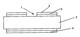
実施例1で作製したβ化率が30%以上の窒化ケイ素質粉末に3wt%MgO、1wt%Y2O3の焼結助剤を添加した混合粉末を作製した。次いで、アミン系の分散剤を2wt%添加したトルエン・ブタノール溶液を満たしたボールミルの樹脂製ポット中に作製した混合粉末および粉砕媒体の窒化ケイ素製ボールを投入し、48時間湿式混合した。次いで、前記ポット中の混合粉末100重量部に対しポリビニル系の有機バインダーを15重量部および可塑剤(ジメチルフタレ−ト)を5重量部添加し、次いで48時間湿式混合しシート成形用スラリーを得た。この成形用スラリーを調整後、ドクターブレード法によりグリーンシート成形した。次いで、成形したグリーンシートを空気中400〜600℃で2〜5時間加熱することにより、予め添加し有機バインダー成分を十分に脱脂(除去)した。次いで脱脂体を0.9MPa(9気圧)の窒素雰囲気中で1850℃×5時間の焼成を行い、次いで同窒素雰囲気中で1900℃×24時間の熱処理を行い、その後室温に冷却した、得られた窒化ケイ素質焼結体シートに機械加工を施し縦50mm×横50mm×厚さ0.6mmの半導体装置用の基板を製造した。この窒化ケイ素質焼結体製基板を用いて図2に示す回路基板を作製した。図2において、回路基板1は作製した前記縦50mm×横50mm×厚さ0.6mmの寸法の窒化ケイ素質焼結体製基板2の表面に銅製回路板3を設け、前記基板2の裏面に銅板4をろう材5により接合して構成されている。この回路基板1に対し、3点曲げ強度の評価および耐熱サイクル試験を行った。その結果、曲げ強度が600MPa以上と大きく、回路基板1の実装工程における締め付け割れおよびはんだ付け工程時の熱応力に起因するクラックの発生する頻度がほぼ見られなくなり、回路基板を使用した半導体装置の製造歩留まりを大幅に改善できることが実証された。また、耐熱サイクル試験は、−40℃での冷却を20分、室温での保持を10分および180℃における加熱を20分とする昇温/降温サイクルを1サイクルとし、これを繰り返し付与し、基板部にクラック等が発生するまでのサイクル数を測定した。その結果、1000サイクル経過後においても窒化ケイ素質焼結体製基板2の割れや銅製回路板2の剥離はなく、優れた耐久性と信頼性を兼備することが確認された。また、1000サイクル経過後においても耐電圧特性の低下は発生しなかった。
【0036】
以上記述の通り、本発明の窒化ケイ素質粉末の製造方法は、凝集したり表面に酸化物が付着することがなく、粉砕ならびに酸処理工程などの面倒で手間の掛かる工程を必要としないので生産性に優れています。また本発明の窒化ケイ素質焼結体の製造方法によれば、窒化ケイ素質焼結体が本来有する高強度/高靭性に加えて高い熱伝導率を具備させることができるので、半導体素子用基板として用いた場合に半導体素子の作動に伴う繰り返しの熱サイクルによって基板にクラックが発生することが少なく、耐熱衝撃性ならびに耐熱サイクル性を著しく向上することができる。
【図面の簡単な説明】
【図1】本発明の代表的な窒化ケイ素質粉末を走査型電子顕微鏡により撮影した写真である。
【図2】本発明の回路基板の要部断面図を示す。
【符号の説明】
1 回路基板、 2 基板、 3 銅製回路板、 4 銅板、 5 ろう材。[0001]
TECHNICAL FIELD OF THE INVENTION
The present invention provides a high strength and high thermal conductivity suitable as a member for electronic components such as a substrate for a semiconductor or a heat sink for a heating element, or a member for a general machine tool, a member for a molten metal, or a structural member such as a member for a heat engine. Rich silicon nitride sintered bodyofProduction methodas well asThe present invention relates to a method for producing a silicon nitride powder suitable for the production.
[0002]
[Prior art]
Silicon nitride sintered bodies have excellent heat resistance, low thermal expansion properties, thermal shock resistance, and corrosion resistance to metals, in addition to mechanical properties such as high-temperature strength properties and wear resistance. It is used for various structural members such as members, members for engines, mechanical members for steelmaking, and melting members of molten metal. In addition, it is used as an electrical insulating material by utilizing high insulating properties.
[0003]
2. Description of the Related Art In recent years, with the development of semiconductor elements having a large amount of heat, such as high-frequency transistors and power ICs, the demand for ceramic substrates having a high thermal conductivity in order to obtain good heat dissipation characteristics in addition to electrical insulation has been increasing. Although an aluminum nitride substrate is used as such a ceramic substrate, there is a problem that mechanical strength, fracture toughness, and the like are low, and cracks are generated by fastening in a process of assembling the substrate unit. Further, in a circuit board in which a Si semiconductor element is mounted on an aluminum nitride substrate, since the thermal expansion difference between Si and the aluminum nitride substrate is large, cracks and cracks occur in the aluminum nitride substrate due to thermal cycling, and mounting reliability is reduced. There's a problem.
[0004]
Therefore, although the thermal conductivity is inferior to the aluminum nitride substrate, the thermal expansion coefficient is close to that of Si, and a substrate made of a high thermal conductive silicon nitride sintered body having excellent mechanical strength, fracture toughness and thermal fatigue resistance has attracted attention. The proposal has been made.
[0005]
For example, Japanese Unexamined Patent Publication No. Hei 4-175268 discloses that silicon and aluminum are substantially composed of silicon nitride, each containing 3.5% by weight or less of Al and oxygen as impurities, and having a density of 3.15Mg / m3 (3.15g). / Cm3) or more, and a silicon nitride sintered body having a thermal conductivity of 40 w / (m · K) or more.
[0006]
Japanese Patent Application Laid-Open No. 9-30866 discloses that 85-99% by weight of β-type silicon nitride grains are composed of a grain boundary phase of oxide or oxynitride, and Mg, Ca, 0.5 to 10% by weight of at least one element selected from Sr, Ba, Y, La, Ce, Pr, Nd, Sm, Gd, Dy, Ho, Er and Yb, Silicon nitride having an Al element content of 1% by weight or less, a porosity of 5% or less, and a proportion of β-type silicon nitride particles having a minor axis diameter of 5 μm or more of 10 to 60% by volume. An elementary sintered body is described.
[0007]
Also, in the proceedings of the Annual Meeting of the Ceramic Society of Japan 1996, 1G11 and 1G12, and JP-A-10-194842, columnar silicon nitride particles or whiskers are added to raw material powder in advance, and a doctor blade method or an extrusion molding method is used. After obtaining a molded body in which these particles are two-dimensionally oriented by using sintering, the sintered body is sintered to impart anisotropy to heat conduction to increase thermal conductivity in a specific direction. Is described.
[0008]
Improve the thermal conductivity of silicon nitride or improve the balance between flexural strength and fracture toughness.FineAs a method for producing a β powder used for constructing a structure, a silicon nitride raw material powder is mixed with a predetermined amount of Y.2O3And SiO2And sintering the mixture in a non-oxidizing atmosphere such as nitrogen. Ceram. Soc. Japan. , 101 [9] 1078-80 (1993).
[0009]
Further, as a method for improving the β fraction of silicon nitride powder, a specific surface area of 1 m2/ G or more, SiO2Japanese Patent Application Laid-Open No. Hei 6-263410 describes a method of heat treating a silicon nitride raw material powder containing 2 to 5% by weight of oxygen in a non-oxidizing atmosphere such as nitrogen.
[0010]
[Problems to be solved by the invention]
In the above-mentioned Japanese Patent Application Laid-Open No. 4-175268, a thermal conductivity of 40 W / (m · K) or more is obtained. However, a material having a higher thermal conductivity and excellent mechanical strength is desired. In the methods described in JP-A-9-30866 and JP-A-10-194842, a seed crystal or a whisker serving as a growth nucleus is used to obtain large columnar particles in a silicon nitride sintered body. And firing in a nitrogen atmosphere of 2000 ° C. or more and 10.1 MPa (100 atm) or more is indispensable. Therefore, special high-temperature and high-pressure equipment such as a hot press or HIP is required, resulting in an increase in cost. Also, since the molding process for obtaining a molded body in which silicon nitride particles are oriented is complicated,sexIs significantly reduced.
[0011]
In addition, the aforementioned J.I. Ceram. Soc. Japan, 101 [9] 1078-80 (1993) describes a method of using Y as a slag.2O3Quantity and SiO2Because of the large amount, the resulting treated powder is strongly agglomerated and must be crushed in a mortar or the like. Also removes oxides adhering to the particle surfaceofAnd a classification process for adjusting the particle size are required, which complicates the process. Further, there is a problem that the used auxiliary component is dissolved in the obtained processed powder.
[0012]
Further, the method described in the above-mentioned Japanese Patent Application Laid-Open No. 6-263410 makes it possible to industrially and inexpensively produce a silicon nitride powder having a β fraction of 95% or more. According to this, as a technique for improving the β fraction,
[0013]
The present invention has been made in view of the above-described conventional problems, and does not require a costly firing method such as high-temperature / high-pressure firing at 2,000 ° C. or higher and 10.1 MPa (100 atm) or higher, and disintegrates the aggregated powder. Provided is a high thermal conductivity type silicon nitride sintered body which has excellent mechanical strength, does not have anisotropy in the direction of heat conduction, and has improved thermal conductivity as compared with the prior art.AlthoughAn object of the present invention is to provide a silicon nitride powder having a high thermal conductivity and a high strength by defining a β fraction, an oxygen content, an impurity amount, a mixing ratio with an α-type silicon nitride powder, and the like. Base sintered bodyofIt is to provide a manufacturing method. Another object of the present invention is to provide a method for producing a silicon nitride powder used for developing high strength and high thermal conductivity.
[0014]
[Means for Solving the Problems]
In order to achieve the above-mentioned object, the present inventors stably specify 100 W / (%) by defining powder characteristics such as a β fraction, an oxygen content, an impurity and a mixing ratio with an α powder of a silicon nitride powder to be used. It has been discovered that a silicon nitride sintered body having a thermal conductivity of at least m · K) and a sufficient bending strength can be obtained. Further, it is effective to improve the sinterability by using a sintering aid as an MgO group and to contain a specific amount of at least one element selected from rare earth elements (RE) containing La, Y and Yb. Discovered and led to the present invention.
[0015]
The silicon nitride-based powder of the present invention is, for example, a metal silicon direct nitridation method, using a silicon nitride-based powder as a raw material by a silica reduction method or a silicon imide decomposition method, in nitrogen or a mixed atmosphere of nitrogen / hydrogen at 1400 ° C to 1950 ° C It can be manufactured by heat treatment for 5 to 20 hours. In order to achieve high β fraction and low oxygen, heat treatment conditions are 1800 ° C ~ 19FiveMore preferably, the temperature is 0 ° C. × 5 to 20 hours. Note that the heat treatment at 1800 ° C. or more is preferably performed in a nitrogen or nitrogen / hydrogen atmosphere of 1.0 MPa (10 atm) or more to avoid decomposition of silicon nitride. In order to reduce the oxygen content after the heat treatment to less than 0.5 wt%, the initial oxygen content is set to SiO2.2It is preferable that the content be less than 2 wt% in terms of amount. In order to minimize the amount of impurities such as Fe and Al, it is more preferable to use a high-purity raw material silicon nitride powder by an imide decomposition method. The container used for filling the raw material powder may be made of carbon or BN. However, if a carbon heater and a heat treatment furnace with a carbon insulating material specification are used, BN is used to suppress the action of an excessive CO reducing atmosphere. Is preferred.
[0016]
Since the silicon nitride powder of the present invention uses a raw material powder having a low oxygen content,
[0017]
Further, in the method for producing a silicon nitride sintered body of the present invention, the β fraction is 30 to 100%.so,Oxygen content is 0.5wt%, Fe content and Al content respectively 100 ppm Less than,Average particle size is 0.2 to 10 μmIn the range ofAspect ratio of 10 or lessColumnar particlesIsβ type1 to 50 parts by weight of silicon nitride-based powder and 0.2 to 4 μm in average particle diameterIn rangeα-type silicon nitride powder 99 to 50 parts by weight,Mg and at least one element selected from rare earth elements (RE) containing La, Y and Yb are respectively converted into magnesium oxide (MgO) and an oxide of a rare earth element compound (RE). x O y ), And the sum of the oxide equivalent contents is 0.6 ~ 7 wt% and (MgO / RE x O y ) Is 1 to 70 Sintering aid, and an organic binder are blended, and a molded body obtained from these is blended. 1650 ~ 1900 In ° CIt is characterized by sintering. When the β-fraction of the silicon nitride powder is less than 30%, although it has an effect as a growth nucleus, it partially acts as a nucleus, so that abnormal grain growth occurs, and the microstructure of the finally obtained silicon nitride sintered body is reduced. Large particles cannot be uniformly dispersed in the tissue, and the flexural strength decreases. Therefore, the β fraction of the silicon nitride powder is desirably 30% or more. If the average particle diameter of the silicon nitride powder is less than 0.2 μm, a silicon nitride sintered body having a microstructure in which columnar particles are uniformly developed cannot be obtained as described above, and the thermal conductivity and the bending strength may be increased. Is difficult. If the average particle diameter of the silicon nitride powder is larger than 10 μm, densification of the silicon nitride of the sintered body is hindered. Therefore, the average particle diameter of the silicon nitride powder is preferably 0.2 to 10 μm. On the other hand, when the aspect ratio is more than 10, the densification of the silicon nitride-based sintered body is hindered, and as a result, the three-point bending strength at room temperature becomes less than 600 MPa. Therefore, the aspect ratio of the silicon nitride powder is set to 10 or less.Columnar particlesIt is preferable that
[0018]
Of the present inventionDepends on manufacturing methodThe silicon nitride sintered body has a β fraction of 30 to 100%, an oxygen content of less than 0.5 wt%, an Fe content and an Al content of 100 ppm or less, and an average particle size of 0.2 to 10 μm, respectively. It consists of 1 to 50 parts by weight of β-type silicon nitride powder, which is a columnar particle having an aspect ratio of 10 or less, and 99 to 50 parts by weight of α-type silicon nitride powder having an average particle diameter in the range of 0.2 to 4 μm. The body contains at least one rare earth element selected from Mg and a rare earth element (RE) containing La, Y and Yb, converts Mg into magnesium oxide (MgO), and contains La, Y and Yb. At least one element selected from the elements (RE) is converted to an oxide (RExOy), The sum of the oxide equivalent contents is 0.6 to 7 wt%, and (MgO / RE)xOy) Is from 1 to 70.AndThe thermal conductivity at room temperature is 100 to 300 W / (m · K), and the three-point bending strength is 600 to 1500 MPa. If the total content in terms of oxide is less than 0.6 wt%, the densification effect during sintering becomes insufficient and the relative density becomes less than 95%, which is not preferable. The amount of the grain boundary phase having a low thermal conductivity as a structural component becomes excessive, and the thermal conductivity of the sintered body becomes less than 100 W / (m · K). The total of these silicon nitride contents is more preferably 0.6 to 4% by weight. The silicon nitride sintered body has a thermal conductivity of 100 to 300 W / (m · K) at room temperature, a three-point bending strength of 600 to 1500 MPa at room temperature, and is rich in high strength and high thermal conductivity. The silicon nitride-based sintered body converts contained Mg into magnesium oxide (MgO), and contains at least one element selected from rare earth elements (RE) containing La, Y and Yb as oxides ( RExOy), The sum of the oxide equivalent contents is 0.6 to 7 wt%, and MgO / RExOyIn particular, when the weight ratio represented by is 1 to 70, high strength and high thermal conductivity are improved. (MgO / RExOyIf the (weight ratio) is less than 1, the proportion of the rare earth oxide in the grain boundary phase increases, so that the liquidus temperature rises in the sintering process, and the sintering becomes difficult, and a dense sintered body cannot be obtained. (MgO / RExOyIf the (weight ratio) exceeds 70, the diffusion of Mg during firing cannot be suppressed, and color unevenness occurs on the surface of the sintered body. When the MgO / RExOy (weight ratio) is in the range of 1 to 70, the preform is fired at a sintering temperature of 1650 to 1850 ° C, and then a heat treatment at 1850 to 1900 ° C is performed, whereby the high thermal conductivity becomes remarkable. A silicon nitride based sintered body exceeding 120 w / (m · K) can be obtained, which is particularly preferable. The increase in thermal conductivity by this heat treatment is due to the combined effect of the growth of silicon nitride particles and the efficient vaporization of the MgO-based grain boundary phase component out of the silicon nitride sintered body with a high vapor pressure.
[0019]
In addition, the present inventionBe involved inThe circuit board converts the contained Mg into magnesium oxide (MgO), and converts at least one element selected from the contained rare earth elements (RE) containing La, Y and Yb into an oxide (RE).xOy) Converted to a silicon nitride sintered body whose total oxide equivalent content is 0.6 to 7% by weight and joined to a circuit board, and which is superior in heat resistance and heat dissipation as compared with the prior art. Can be provided.
[0020]
BEST MODE FOR CARRYING OUT THE INVENTION
0.5% by weight of oxygen in the silicon nitride powderLess thanThe reason is that when the silicon nitride-based powder is used as a growth nucleus to form a silicon nitride-based sintered body, the amount of oxygen dissolved in the silicon nitride-based particles constituting the silicon nitride-based sintered body is: It depends strongly on the oxygen content of the silicon nitride powder used as a growth nucleus, and the higher the oxygen content of the silicon nitride powder, the higher the amount of oxygen dissolved in the silicon nitride particles. Oxygen contained in the silicon nitride-based particles causes scattering of phonons, which are a heat-conducting medium, and lowers the thermal conductivity of the silicon nitride-based sintered body. 100 W / m. In order to express a high thermal conductivity that cannot be obtained with the conventional silicon nitride sintered body of not less than K, the oxygen content of the silicon nitride powder is set to 0.5 wt%.Less thanIt is essential to reduce the amount of oxygen in the silicon nitride sintered body finally obtained.
[0021]
When the Fe content and the Al content in the silicon nitride-based powder are more than 100 ppm, Fe or Al remarkably forms a solid solution in the silicon nitride particles. Reduce the thermal conductivity of the silicon-based sintered body. Therefore, in order to obtain a thermal conductivity of 100 W / m · K or more, it is important to control the Fe content and the Al content in the silicon nitride powder to 100 ppm or less, respectively.
[0022]
The ratio between the silicon nitride powder having a β fraction of 30 to 100% and the α-type silicon nitride powder is preferably 1 to 50% by weight: 99 to 50% by weight. When the ratio of the silicon nitride-based powder having a β fraction of 30 to 100% is less than 1 wt%, although there is an effect as a growth nucleus, the number of growth nuclei acting due to a small addition amount is small, and abnormal grain growth occurs. Large particles cannot be uniformly dispersed in the microstructure, and the bending strength decreases. On the other hand, if it exceeds 50 wt%, the number of growth nuclei increases, and in the course of grain growth, particles collide with each other, thereby inhibiting growth and maintaining strength. However, the silicon nitride sintered body composed of developed columnar particles can be maintained. Cannot be obtained, and it becomes difficult to realize a high thermal conductivity as compared with the related art.
[0023]
Mg and Y are useful as sintering aids and are effective for densification of silicon nitride-based raw material powder. Since these elements have a low solid solubility in silicon nitride particles as the first microstructure component constituting the silicon nitride sintered body, the thermal conductivity of the silicon nitride particles, and thus the silicon nitride sintered body, is high. Can be kept.
[0024]
Like Y, it has a low solid solubility in silicon nitride particles and is useful as a sintering aid as an element such as La, Ce, Nd, Pm, Sm, Eu, Gd, Dy, Ho, Er, Tm, Yb, and Lu. At least one rare earth element selected from the group of Among them, at least one rare earth element selected from the group consisting of La, Ce, Gd, Dy, and Yb is preferable because firing can be performed without increasing the temperature and pressure too much.
[0025]
The substrate made of the silicon nitride-based sintered body of the present invention makes use of the characteristics of high strength, high toughness and high thermal conductivity, and is used for various substrates such as a substrate for a power semiconductor or a substrate for a multi-chip module, or for a Peltier device. It is suitable for a member for electronic components such as a heat transfer plate or a heat sink for various heating elements.
[0026]
When the silicon nitride-based sintered body of the present invention is used as a substrate for a semiconductor element, the occurrence of cracks in the substrate when subjected to repeated thermal cycles accompanying the operation of the semiconductor element is suppressed, and the thermal shock resistance and the heat cycle Properties are remarkably improved, and excellent reliability is obtained. In addition, even when a semiconductor element for high output and high integration is mounted, deterioration of thermal resistance characteristics is small and excellent heat radiation characteristics are exhibited. Furthermore, the excellent mechanical properties allow not only the function as the original substrate material but also the structure itself to serve as a structural member, so that the structure of the substrate unit itself can be simplified.
[0027]
Further, the silicon nitride sintered body of the present invention can be widely used for materials requiring heat resistance properties such as thermal shock and thermal fatigue, in addition to the above-mentioned electronic component members. Structural members include various heat exchanger parts and heat engine parts, heater tubes used in the field of melting metals such as aluminum and zinc, Stokes, die-cast sleeves, propellers for molten metal agitation, ladles, thermocouple protection tubes, etc. Applicable to Further, by applying the present invention to a sink roll, a support roll, a bearing, a shaft, or the like used in a hot-dip metal plating line for aluminum, zinc, or the like, a member having high crack resistance against rapid heating and cooling can be obtained. In addition, in the field of steel or non-ferrous processing, if it is used for rolling rolls, squeeze rolls, guide rollers, drawing dies, or tool tips, it has good heat dissipation properties when it comes into contact with the work piece, so it has good thermal fatigue resistance. In addition, thermal shock resistance can be improved, whereby wear is reduced and thermal stress cracking is less likely to occur.
[0028]
Further, the present invention can be applied to a sputter target member, for example, forming an electric insulating film used for an MR head, a GMR head, or a TMR head of a magnetic recording device, and forming a wear-resistant film used for a thermal head of a thermal transfer printer. It is suitable for. The coating obtained by sputtering has essentially high thermal conductivity, a sufficiently high sputter rate, and a high electrical withstand voltage of the coating. For this reason, the electrical insulating coating for the MR head, GMR head, or TMR head formed with this sputter target has characteristics of high thermal conductivity and high withstand voltage, so that the heat generation density of the element can be increased and the insulating coating can be made thinner. Can be achieved. In addition, the wear-resistant coating for a thermal head formed with this sputter target has not only good wear resistance due to the inherent characteristics of silicon nitride but also high thermal conductivity, so that thermal resistance can be reduced. Can be enhanced.
[0029]
【Example】
Hereinafter, the present invention will be described with reference to examples, but the present invention is not limited to the examples.
(Example 1)
Oxygen content is SiO2A BN crucible is filled with an imide decomposition silicon nitride powder having an average particle diameter of 0.2 to 2.0 μm in terms of less than 2.0 wt% in terms of conversion, and then N at normal pressure to 1.0 MPa (10 atm).2Heat treatment was performed at 1400 ° C. to 1950 ° C. for 1 to 20 hours in an atmosphere, and then cooled to room temperature. The β fraction of the obtained silicon nitride-based powder was 90 to 100%, and the oxygen content was 0.2 to 0.4% by weight. FIG. 1 shows an SEM observation image of the obtained silicon nitride-based powder example. The powder has a β fraction of 100%, an oxygen content of 0.2 wt%, and Fe and Al contents of 50 ppm and 40 ppm, respectively. Grooves are formed in the powder in parallel to the major axis direction of the particles, which is a feature when grain growth occurs through the gas phase, and it has been demonstrated that the smaller the amount of oxygen is, the more significant it becomes. Was. Following the powder, the obtained β-type Si3N45 to 30 parts by weight of a powder of silicon nitride based on α-type silicon nitride (Si) having an oxygen content of 0.3 to 1.5 wt% and an average particle diameter of 0.5 μm.3N49) to 66 parts by weight of a powder, MgO powder having an average particle size of 0.2 μm as a sintering aid, and RE having an average particle size of 0.2 to 2.0 μm described in Table 1.xOyThe powder (sintering aid) was blended, and a 2 wt% dispersant (Leogard GP) was further blended and charged into a ball mill container filled with ethanol, and then mixed. The resulting mixture is dried in vacuo and thenμ mAnd granulated through a sieve. Next, a disk-shaped molded body having a diameter of 20 mm × a thickness of 10 mm and a diameter of 100 mm × a thickness of 15 mm was obtained by CIP molding under a pressure of 3 ton with a press machine. Next, firing was performed in a nitrogen gas atmosphere at 1750 to 1900 ° C. and 0.9 MPa (9 atm) for 5 hours. The impurities of Fe and Al in the obtained silicon nitride powder were analyzed by a plasma emission spectrometry (ICP) method. The oxygen content was measured by an infrared heating absorption method. The β fraction of the obtained silicon nitride-based powder was determined from the X-ray diffraction intensity ratio using Cu-Kα ray according to the formula (1).
Iβ (210) : Β-type Si3N4(210) plane diffraction peak intensity,
Iα (102) : Α-type Si3N4(102) surface diffraction peak intensity of
Iα (210) : Α-type Si3N4(210) surface diffraction peak intensity.
The average particle diameter and average aspect ratio of the obtained silicon nitride-based powder were determined by using an SEM photograph obtained at an observation magnification of × 2000 by SEM observation to obtain a total of 500 nitrided particles within a visual area of 200 μm × 500 μm. The silicon particles were randomly selected, the minimum diameter and the maximum diameter were measured by an image analyzer, and the average value was obtained and evaluated. Next, from the obtained silicon nitride sintered body, a test piece having a diameter of 10 mm × thickness of 3 mm for measuring thermal conductivity and density, and a bending test piece having a length of 3 mm × 4 mm × a length of 40 mm were collected. The density was calculated by measuring the size with a micrometer and measuring the weight. The thermal conductivity was determined by measuring the specific heat and the thermal diffusivity at room temperature by a laser flash method and calculating the thermal conductivity. The three-point bending strength was measured at room temperature in accordance with JIS R1606. The outline of the above manufacturing conditions and the evaluation results are shown in Tables 1 and 2 for sample No. 1 to 11.
[0030]
(Comparative Example 1)
Silicon nitride powders having different β fractions were prepared in the same manner as in Example 1 except that the production conditions described in Table 1 were used. Next, a silicon nitride-based sintered body was prepared using the obtained silicon nitride-based powder and evaluated. The outline of the above manufacturing conditions and the evaluation results are shown in Tables 1 and 2 for sample No. 31 to 41 show.
[0031]
[Table 1]
[Table 2]
Table 1 and Table 2 sample No. From 1 to 11, the following findings were obtained.
The average particle size of the silicon nitride powder added as growth nuclei is such that the β fraction is 30% or more, the oxygen content as impurities is 0.5 wt% or less, the Fe content is 100 ppm or less, and the Al content is 100 ppm or less. The silicon nitride-based sintered body obtained by setting the blending amount of the silicon nitride-based powder having a diameter of 0.2 to 10 μm, an aspect ratio of 10 or less, and a β conversion ratio of 30% or more to 1 to 50 wt% at room temperature The thermal conductivity becomes 100 w / (m · K) or more, and the three-point bending strength at room temperature becomes 600 MPa or more. The thermal conductivity of the silicon nitride sintered body according to the prior art was about 40 w / (m · K), and the thermal conductivity could be dramatically increased. Further, as a sintering aid, Mg is converted to magnesium oxide (MgO), and Y, La, Ce, Dy, Gd and Yb are converted to oxides (RExOy), The sum of the oxide equivalent contents is 0.6 to 7.0 wt%, and (MgO / RE)xOy) (Weight ratio) of 1 to 70 had a thermal conductivity of 100 w / (m · K) or more and a bending strength of 600 MPa or more.
[0034]
On the other hand, the sample Nos. The following findings were obtained from 31 to 41.
No. In the case of No. 31, when the β fraction of the silicon nitride particles is less than 30%, the bending strength is remarkably reduced to about 500 MPa.
No. In No. 32, when the amount of oxygen inevitably contained in the silicon nitride powder exceeds 0.5 wt., The thermal conductivity is reduced to 70 w / (m · K) or less.
No. 33 and No. 33. In No. 34, when the content of each of the impurities Fe and Al contained in the silicon nitride-based powder exceeds 100 ppm, the thermal conductivity decreases to 65 w / (m · K) or less.
No. 35 and No. 35. In No. 36, when the average particle diameter of the silicon nitride-based powder is less than 0.2 μm, the thermal conductivity is reduced to 60 w / (m · K) or less. The conductivity becomes 60 w / (m · K) or less, and the bending strength decreases to 600 MPa or less.
No. In No. 37, when the aspect ratio of the silicon nitride powder was 10 or more, a dense sintered body was not obtained, and the bending strength was reduced to 600 MPa or less.
No. 38 and No. 38. In No. 39, when the addition amount of the silicon nitride-based powder was less than 1.0 wt%, the bending strength was reduced to 600 MPa or less, and when it was more than 50 wt%, the thermal conductivity was reduced to 70 w / (m · K) or less.
No. 40 and No. In No. 41, when the sintering aid component was less than 0.6 wt%, the density of the sintered body was reduced, and as a result, the thermal conductivity and the bending strength were significantly reduced. When the sintering aid component exceeds 7.0 wt%, a sufficient glass phase is generated in the firing process, so that the sintered body is densified, but on the other hand, the grain boundary phase which is a low heat conductive phase increases. As a result, the thermal conductivity was reduced to 60 w / (m · K) or less.
[0035]
(Example 2)
3 wt% MgO and 1 wt% Y were added to the silicon nitride powder having a β conversion ratio of 30% or more prepared in Example 1.2O3A mixed powder to which the sintering aid was added was prepared. Then, the mixed powder thus produced and a silicon nitride ball as a grinding medium were put into a resin pot of a ball mill filled with a toluene / butanol solution containing 2 wt% of an amine-based dispersant, and wet-mixed for 48 hours. Next, 15 parts by weight of a polyvinyl organic binder and 5 parts by weight of a plasticizer (dimethylphthalate) were added to 100 parts by weight of the mixed powder in the pot, and then wet-mixed for 48 hours to obtain a sheet forming slurry. . After adjusting the molding slurry, green sheets were formed by a doctor blade method. Next, the formed green sheet was heated in air at 400 to 600 ° C. for 2 to 5 hours to add in advance and sufficiently degrease (remove) the organic binder component. Next, the degreased body was fired at 1850 ° C. for 5 hours in a nitrogen atmosphere of 0.9 MPa (9 atm), then heat-treated at 1900 ° C. for 24 hours in the nitrogen atmosphere, and then cooled to room temperature. The silicon nitride-based sintered body sheet was subjected to machining to produce a semiconductor device substrate having a length of 50 mm, a width of 50 mm and a thickness of 0.6 mm. A circuit board shown in FIG. 2 was produced using the silicon nitride sintered body substrate. In FIG. 2, a
[0036]
As described above, the silicon nitride powder of the present inventionProduction methodHas excellent productivity because it does not agglomerate or adhere oxides to the surface, and does not require laborious and laborious processes such as grinding and acid treatment. Further, the silicon nitride sintered body of the present inventionAccording to the manufacturing method of,Silicon nitride sintered bodyHigh thermal conductivity in addition to the inherent high strength / high toughnessBecause you canIn addition, when used as a substrate for a semiconductor element, cracks are less likely to occur in the substrate due to repeated thermal cycling accompanying the operation of the semiconductor element, and the thermal shock resistance and the thermal cycle resistance can be significantly improved.
[Brief description of the drawings]
FIG. 1 is a photograph of a representative silicon nitride powder of the present invention taken with a scanning electron microscope.
FIG. 2 is a sectional view of a main part of the circuit board of the present invention.
[Explanation of symbols]
1 circuit board, 2 boards, 3 copper circuit board, 4 copper board, 5 brazing material.
Claims (3)
Priority Applications (9)
| Application Number | Priority Date | Filing Date | Title |
|---|---|---|---|
| JP2000284957A JP3565425B2 (en) | 2000-09-20 | 2000-09-20 | Method for producing silicon nitride-based powder and method for producing silicon nitride-based sintered body |
| DE2001165080 DE10165080B4 (en) | 2000-09-20 | 2001-09-19 | Silicon nitride powder and sintered body and method of making the same and printed circuit board therewith |
| DE10146227.1A DE10146227B4 (en) | 2000-09-20 | 2001-09-19 | Silicon nitride sintered body, printed circuit board and thermoelectric module |
| DE10165107.4A DE10165107B3 (en) | 2000-09-20 | 2001-09-19 | Substrate with silicon nitride sintered body and printed circuit board |
| CNB011379634A CN1192989C (en) | 2000-09-20 | 2001-09-20 | Silicon nitride powder, its sintered body, substrate and circuit board and thermoelectric element module thereof |
| US09/956,033 US6846765B2 (en) | 2000-09-20 | 2001-09-20 | Silicon nitride powder, silicon nitride sintered body, sintered silicon nitride substrate, and circuit board and thermoelectric module comprising such sintered silicon nitride substrate |
| KR1020010058380A KR100833962B1 (en) | 2000-09-20 | 2001-09-20 | Silicon nitride powder, sintered silicon nitride, sintered silicon nitride substrate, and circuit board and thermoelectric element module comprising such sintered silicon nitride substrate |
| US10/998,657 US7031166B2 (en) | 2000-09-20 | 2004-11-30 | Silicon nitride powder, silicon nitride sintered body, sintered silicon nitride substrate, and circuit board and thermoelectric module comprising such sintered silicon nitride substrate |
| KR1020070095109A KR100836150B1 (en) | 2000-09-20 | 2007-09-19 | Sintered silicon nitride, method of manufacturing the same and sintered silicon nitride substrate |
Applications Claiming Priority (1)
| Application Number | Priority Date | Filing Date | Title |
|---|---|---|---|
| JP2000284957A JP3565425B2 (en) | 2000-09-20 | 2000-09-20 | Method for producing silicon nitride-based powder and method for producing silicon nitride-based sintered body |
Related Child Applications (1)
| Application Number | Title | Priority Date | Filing Date |
|---|---|---|---|
| JP2004130790A Division JP4089974B2 (en) | 2004-04-27 | 2004-04-27 | Silicon nitride powder, silicon nitride sintered body, and circuit board for electronic components using the same |
Publications (3)
| Publication Number | Publication Date |
|---|---|
| JP2002097005A JP2002097005A (en) | 2002-04-02 |
| JP2002097005A5 JP2002097005A5 (en) | 2004-08-05 |
| JP3565425B2 true JP3565425B2 (en) | 2004-09-15 |
Family
ID=18769101
Family Applications (1)
| Application Number | Title | Priority Date | Filing Date |
|---|---|---|---|
| JP2000284957A Expired - Lifetime JP3565425B2 (en) | 2000-09-20 | 2000-09-20 | Method for producing silicon nitride-based powder and method for producing silicon nitride-based sintered body |
Country Status (1)
| Country | Link |
|---|---|
| JP (1) | JP3565425B2 (en) |
Families Citing this family (18)
| Publication number | Priority date | Publication date | Assignee | Title |
|---|---|---|---|---|
| JP3797905B2 (en) * | 2000-10-27 | 2006-07-19 | 株式会社東芝 | Silicon nitride ceramic substrate, silicon nitride ceramic circuit substrate using the same, and manufacturing method thereof |
| JP4518020B2 (en) * | 2005-12-26 | 2010-08-04 | 日立金属株式会社 | A silicon nitride sintered body and a circuit board using the same. |
| JP5200741B2 (en) * | 2007-08-01 | 2013-06-05 | 三菱化学株式会社 | Crystalline silicon nitride and method for producing the same, and phosphor using the same, phosphor-containing composition, light emitting device, lighting device, image display device, sintered body, and pigment |
| US8304935B2 (en) | 2008-09-27 | 2012-11-06 | Witricity Corporation | Wireless energy transfer using field shaping to reduce loss |
| US9184595B2 (en) | 2008-09-27 | 2015-11-10 | Witricity Corporation | Wireless energy transfer in lossy environments |
| US8324759B2 (en) | 2008-09-27 | 2012-12-04 | Witricity Corporation | Wireless energy transfer using magnetic materials to shape field and reduce loss |
| EP2377839B1 (en) | 2009-01-13 | 2016-10-26 | Hitachi Metals, Ltd. | Silicon nitride substrate manufacturing method |
| JP2010173877A (en) * | 2009-01-28 | 2010-08-12 | Taiheiyo Cement Corp | Silicon nitride sintered compact |
| JP5289090B2 (en) * | 2009-02-16 | 2013-09-11 | 太平洋セメント株式会社 | Ceramic material |
| EP2610217A4 (en) * | 2010-08-04 | 2016-02-24 | Ube Industries | SILICON NITRIDE POWDER FOR SILICONITRIDE PHOSPHOR, CaAlSiN3 PHOSPHOR USING SAME, Sr2Si5N8 PHOSPHOR USING SAME, (Sr, Ca)AlSiN3 PHOSPHOR USING SAME, La3Si6N11 PHOSPHOR USING SAME, AND METHODS FOR PRODUCING THE PHOSPHORS |
| JP5874635B2 (en) * | 2010-08-19 | 2016-03-02 | 宇部興産株式会社 | Silicon nitride powder for silicon nitride phosphor, Sr3Al3Si13O2N21 phosphor using the same, β-sialon phosphor and method for producing the same |
| WO2012090542A1 (en) | 2010-12-28 | 2012-07-05 | 宇部興産株式会社 | Polycrystalline silicon ingot casting mold and method for producing same, and silicon nitride powder for mold release material for polycrystalline silicon ingot casting mold and slurry containing same |
| JP5854051B2 (en) * | 2011-10-12 | 2016-02-09 | 宇部興産株式会社 | Oxynitride phosphor powder and method for producing the same |
| KR101794410B1 (en) * | 2015-08-17 | 2017-11-07 | 한국과학기술원 | Sintered silicon nitride having high thermal conductivity and Manufacturing method thereof |
| JP6729224B2 (en) * | 2015-11-26 | 2020-07-22 | 三菱マテリアル株式会社 | Ceramic/aluminum bonded body, insulated circuit board, power module, LED module, thermoelectric module |
| KR102067144B1 (en) * | 2017-06-26 | 2020-01-16 | 주식회사 엘지화학 | Method for preparing silicon nitride sintered body, silicon nitride sintered body and heat radiation substrate using the same |
| KR101901172B1 (en) * | 2018-05-23 | 2018-09-27 | (주)존인피니티 | High thermal conductive silicon nitride ceramics substrate with excellent electric isolation |
| WO2023176500A1 (en) * | 2022-03-16 | 2023-09-21 | 株式会社 東芝 | Silicon nitride sintered body and wear-resistant member using same |
Family Cites Families (4)
| Publication number | Priority date | Publication date | Assignee | Title |
|---|---|---|---|---|
| JPH0829923B2 (en) * | 1989-12-07 | 1996-03-27 | 電気化学工業株式会社 | Silicon nitride powder |
| JP3486642B2 (en) * | 1992-11-27 | 2004-01-13 | 独立行政法人物質・材料研究機構 | High Purification Processing Method of Silicon Nitride Raw Material Powder |
| JP3501317B2 (en) * | 1995-07-21 | 2004-03-02 | 日産自動車株式会社 | High thermal conductivity silicon nitride sintered body and insulating substrate made of silicon nitride sintered body |
| JPH11349381A (en) * | 1998-06-08 | 1999-12-21 | Hitachi Metals Ltd | Silicon nitride sintered compact and sputter target comprising the same |
-
2000
- 2000-09-20 JP JP2000284957A patent/JP3565425B2/en not_active Expired - Lifetime
Also Published As
| Publication number | Publication date |
|---|---|
| JP2002097005A (en) | 2002-04-02 |
Similar Documents
| Publication | Publication Date | Title |
|---|---|---|
| JP3565425B2 (en) | Method for producing silicon nitride-based powder and method for producing silicon nitride-based sintered body | |
| KR100833962B1 (en) | Silicon nitride powder, sintered silicon nitride, sintered silicon nitride substrate, and circuit board and thermoelectric element module comprising such sintered silicon nitride substrate | |
| JP2007197229A (en) | High-thermal conductive silicon nitride substrate and method of manufacturing the same | |
| JP2002201075A (en) | Silicon nitride ceramic substrate and silicon nitride ceramic circuit substrate using it and its manufacturing method | |
| JP7062229B2 (en) | Plate-shaped silicon nitride sintered body and its manufacturing method | |
| JP2002293642A (en) | Silicon nitride-based sintered compact having high thermal conductivity, method of producing the same, and circuit board | |
| JP2002097005A5 (en) | ||
| JP2002249379A (en) | Aluminum nitride sintered compact and member for device for manufacturing of semiconductor | |
| JP2002265276A (en) | Silicon nitride powder and silicon nitride sintered compact | |
| JP4089974B2 (en) | Silicon nitride powder, silicon nitride sintered body, and circuit board for electronic components using the same | |
| JP4518020B2 (en) | A silicon nitride sintered body and a circuit board using the same. | |
| JP3775335B2 (en) | Silicon nitride sintered body, method for producing silicon nitride sintered body, and circuit board using the same | |
| WO2005049525A1 (en) | High thermally conductive aluminum nitride sintered product | |
| JP4556162B2 (en) | Silicon nitride-based sintered body, method for producing the same, and circuit board using the same | |
| JP4529102B2 (en) | High thermal conductivity silicon nitride sintered body and manufacturing method thereof | |
| JP3002642B2 (en) | Silicon nitride powder, silicon nitride sintered body, and circuit board using the same | |
| JP3100892B2 (en) | High thermal conductive silicon nitride sintered body and method for producing the same | |
| JP4348659B2 (en) | High thermal conductivity silicon nitride sintered body, substrate using the same, circuit board for semiconductor device | |
| JPH09268069A (en) | Highly heat conductive material and its production | |
| JPH11100274A (en) | Silicon nitride sintered compact, its production and circuit board | |
| JP4332828B2 (en) | High thermal conductivity silicon nitride sintered body, substrate using the same, circuit board for semiconductor device | |
| JP3145519B2 (en) | Aluminum nitride sintered body | |
| JP2008156142A (en) | Aluminum nitride sintered compact and method for manufacturing the same | |
| JP2002029851A (en) | Silicon nitride composition, method for manufacturing sintered silicon nitride compact using the same and sintered silicon nitride compact | |
| JP2001019557A (en) | Silicon nitride sintered compact, its production and substrate |
Legal Events
| Date | Code | Title | Description |
|---|---|---|---|
| A975 | Report on accelerated examination |
Free format text: JAPANESE INTERMEDIATE CODE: A971005 Effective date: 20031224 |
|
| A131 | Notification of reasons for refusal |
Free format text: JAPANESE INTERMEDIATE CODE: A131 Effective date: 20040305 |
|
| A521 | Written amendment |
Free format text: JAPANESE INTERMEDIATE CODE: A523 Effective date: 20040427 |
|
| TRDD | Decision of grant or rejection written | ||
| A01 | Written decision to grant a patent or to grant a registration (utility model) |
Free format text: JAPANESE INTERMEDIATE CODE: A01 Effective date: 20040521 |
|
| A61 | First payment of annual fees (during grant procedure) |
Free format text: JAPANESE INTERMEDIATE CODE: A61 Effective date: 20040603 |
|
| R150 | Certificate of patent or registration of utility model |
Free format text: JAPANESE INTERMEDIATE CODE: R150 Ref document number: 3565425 Country of ref document: JP Free format text: JAPANESE INTERMEDIATE CODE: R150 |
|
| FPAY | Renewal fee payment (event date is renewal date of database) |
Free format text: PAYMENT UNTIL: 20080618 Year of fee payment: 4 |
|
| FPAY | Renewal fee payment (event date is renewal date of database) |
Free format text: PAYMENT UNTIL: 20090618 Year of fee payment: 5 |
|
| FPAY | Renewal fee payment (event date is renewal date of database) |
Free format text: PAYMENT UNTIL: 20100618 Year of fee payment: 6 |
|
| FPAY | Renewal fee payment (event date is renewal date of database) |
Free format text: PAYMENT UNTIL: 20100618 Year of fee payment: 6 |
|
| FPAY | Renewal fee payment (event date is renewal date of database) |
Free format text: PAYMENT UNTIL: 20110618 Year of fee payment: 7 |
|
| FPAY | Renewal fee payment (event date is renewal date of database) |
Free format text: PAYMENT UNTIL: 20110618 Year of fee payment: 7 |
|
| FPAY | Renewal fee payment (event date is renewal date of database) |
Free format text: PAYMENT UNTIL: 20120618 Year of fee payment: 8 |
|
| FPAY | Renewal fee payment (event date is renewal date of database) |
Free format text: PAYMENT UNTIL: 20120618 Year of fee payment: 8 |
|
| FPAY | Renewal fee payment (event date is renewal date of database) |
Free format text: PAYMENT UNTIL: 20130618 Year of fee payment: 9 |
|
| EXPY | Cancellation because of completion of term |