JP3539110B2 - Oscillation circuit, semiconductor device, and portable electronic device and clock provided with these - Google Patents
Oscillation circuit, semiconductor device, and portable electronic device and clock provided with these Download PDFInfo
- Publication number
- JP3539110B2 JP3539110B2 JP02728097A JP2728097A JP3539110B2 JP 3539110 B2 JP3539110 B2 JP 3539110B2 JP 02728097 A JP02728097 A JP 02728097A JP 2728097 A JP2728097 A JP 2728097A JP 3539110 B2 JP3539110 B2 JP 3539110B2
- Authority
- JP
- Japan
- Prior art keywords
- oscillation
- circuit
- voltage
- constant voltage
- inverter
- Prior art date
- Legal status (The legal status is an assumption and is not a legal conclusion. Google has not performed a legal analysis and makes no representation as to the accuracy of the status listed.)
- Expired - Fee Related
Links
Images
Landscapes
- Electric Clocks (AREA)
- Electromechanical Clocks (AREA)
Description
【0001】
【発明の属する技術分野】
本発明は、発振回路、半導体装置及びそれらを具備した携帯用の電子機器および時計に関する。
【0002】
【背景技術】
従来より、時計や携帯用の電話、コンピュータ端末などには、水晶振動子を用いた発振回路が広く用いられている。このような携帯用の電子機器または時計では、消費電力を節約し、電池の長寿命化を図ることが必要となる。
【0003】
消費電力の節約という観点から、本発明者は、携帯用電子機器、特に腕時計に使用される電子回路の消費電力を分析した。この分析により、プリント基板上に構成される電子回路のうち、半導体装置においては発振回路部分の消費電力が他の回路部分に比べ大きな割合を占めることが確認された。すなわち、携帯用電子機器に使用される電子回路の発振回路部分での消費電力を節減することが、使用電池の長寿命化を図る上で効果的であることを見出した。
【0004】
図11には、従来の水晶発振回路および定電圧発生回路の一例が示されている。
【0005】
この水晶発振回路は、水晶振動子X’talと、発振用インバータINV0と、フィードバック回路を構成する高抵抗Rfとを含んで構成される。前記フィードバック回路は、抵抗Rf以外に、位相補償用のコンデンサCD,CGを含んで構成され、発振用インバータINV0のドレイン出力を、180度位相反転されたゲート入力として発振用インバータINV0のゲートへフィードバック入力するものである。
【0006】
従来このような水晶発振回路に用いられる発振用インバータINV0は、一対のP型電界効果トランジスタ(以下PMOSと記す)QP0,N型電界効果トランジスタ(以下NMOSと記す)QN0を含み、各PMOSQP0,NMOSQN0のゲートが入力側、ドレインが出力側として機能するように構成されている。そして、前記各トランジスタQP0,QN0は、そのドレイン側が互いに接続され、そのソース側がそれぞれ接地電圧Vdd側,負の定電圧Vreg側に接続されている。
【0007】
以上の構成の水晶発振回路では、発振用インバータINV0に定電圧Vregを印加すると、前記発振用インバータINV0の出力が180度位相反転されてゲートにフィードバック入力される。これにより、発振用インバータINV0を構成するPMOSQP0,NMOSQN0が交互にオンオフ駆動され、水晶発振回路の発振出力が次第に増加し、ついには水晶振動子X’talが安定した発振動作を行なうようになる。
【0008】
しかし、従来の水晶発振回路では、起動時にも、安定発振後にも、常にPMOSQP0,NMOSQN0両トランジスタを交互にオンオフ駆動するように構成されているため、以下に記述する問題があった。
【0009】
従来の水晶発振回路では、安定発振後にも常にPMOSQP0,NMOSQN0を交互にオンオフ駆動している。この場合、前記PMOSQP0をオン駆動しているときには、水晶振動子X’talに充電されたエネルギーのほとんどをそのまま放電する。したがって、次の充電サイクルにおいて、水晶振動子X’talをはじめから充電しなければならず、本発明者は、この充電が、回路全体の電力消費を節減する上の大きな問題となることを見出した。
【0010】
すなわち、水晶発振回路が安定して発振している状態では、水晶振動子X’talに充電された電力を充放電サイクルにおいて完全に放電しなくても、安定した発振状態を維持することができる。しかし、従来の回路では、この充放電サイクルにおいて、水晶振動子X’talの充電電力をそのまま放電し、再度充電するというサイクルを繰り返していたため、これが回路全体の電力消費を増加させる大きな要因となっていた。
【0011】
また、このような水晶発振回路においては、発振停止電圧の絶対値|Vsto|は、前記NMOSQN0の閾値電圧をVthn0,前記PMOSのQP0閾値電圧をVthp0とすると、式1のように表わすことができる。
【0012】
式1:|Vsto|=K・(|Vthp0|+Vthn0)
ここで、定数Kは0.8〜0.9であり、|Vthp0|はVthp0の絶対値を示す。このように、発振停止電圧Vstoは、前記NMOSトランジスタの閾値電圧Vthn0,前記PMOSの閾値電圧Vthp0に依存する。
【0013】
一方、定電圧発生回路は、オペアンプOPと、マイナス(以下−と記す)入力電圧制御用PMOSQP2とプラス(以下+と記す)入力電圧制御用NMOSQN2,出力用NMOSQN1とを含んで構成されている。すなわち、前記オペアンプOPの−入力端子が、ゲートがドレインと接続され、かつ定電流源と電源電圧Vss間に設けられたPMOSQP2のドレインと接続される。さらに、前記オペアンプOPの+入力端子が、ゲートがドレインと短絡され、かつ定電流源と電源電圧Vssの間に設けられたNMOSQN2のドレインと接続されている。
【0014】
そして、前記NMOSQN2のソースとそのドレインが直列に接続され、かつ前記オペアンプOPの出力をゲートに受け、ソースが電源電圧Vssと接続された、出力用のNMOSQN1が設けられている。よって、前記オペアンプOPの出力電圧、すなわち、定電圧発生回路の出力電圧Vregは、前記PMOSQP2およびNMOSQN2のそれぞれの閾値電圧Vthp2,Vthn2の影響をそれぞれ受ける。
【0015】
つまり、この回路の動作について以下に説明すると、前記PMOSQP2に定電流が流れることによって、信号線100に前記PMOSQP2の閾値電圧|Vthp2|に依存した電圧α|Vth p2|(α:定数)が生じる。そして、前記オペアンプOPとNMOSQN1により、信号線101は、前記信号線100と同一の電位α|Vthp2|に制御される。さらに、NMOSQN2に定電流源からの電流が流れることによって、前記信号線101と出力ライン102との間に閾値電圧Vthn2に依存したαVthn2の電位差が生じる。よって、前記出力ライン102と接地電位Vddの間には、|Vthp2|+Vthn2に依存した定電圧α(|Vthp2|+Vthn2)が生じる。
【0016】
よって、オペアンプOPの出力電圧、すなわち、定電圧発生回路の出力電圧Vregは、前記PMOSQP2の閾値電圧Vthp2およびNMOSQN2の閾値電圧Vthn2の影響をそれぞれ受ける。すなわち、定電圧|Vreg|は|Vthp2|+Vthn2に比例する。したがって、従来の構成の水晶発振回路は、|Vthp2|+Vthn2に依存した定電圧値Vregを電源として動作することになる。
【0017】
したがって、従来の定電圧発生回路においては、半導体製造プロセス上で閾値電圧Vthp2及びVthn2の値がばらついて、|Vthp2|もしくはVthn2の値が大きくなった場合でも、定電圧|Vreg|も同時に大きくなるので、常に定電圧Vregと発振停止電圧Vstoの関係において|Vreg|>|Vsto|が保たれ、発振動作確保ができ、ICの歩留りを向上することができるという利点があった。
【0018】
そして、発振回路の低消費電力動作のために、従来は定電圧発生回路を動作させる定電流源を、前記定電圧発生回路が動作可能な範囲で、できるだけ少なくしていた。しかしながら、前述したような携帯用の機器の発展によるニーズに伴い、発振用インバータの低消費電力化を図るために、発振動作確保(|Vreg|>|Vsto|)を満足しつつ、定電圧|Vreg|をできるだけ下げるということが必要となってきた。しかし、定電圧発生回路を動作させる定電流源からの定電流を少なくしていくと、温度変化により定電流が変動した場合の定電圧Vregの変化が大きくなる。
【0019】
ここで、トランジスタの温度特性について、図11に示される定電圧発生回路を用いて説明する。この定電圧発生回路において、NMOSQN2,PMOSQP2を動作させる定電流源TA,TBの電流値には温度依存性がある。すなわち、前記定電流源TA,TBは、例えば、デプリーションタイプのPMOSにより構成されている場合、定電流IDは式2にて表わすことができる。ここで、前記定電流源を構成するデプリーションPMOSの電流増幅率をβとし、その閾値電圧の絶対値を|Vth|とし、ゲート−ソース間電圧をVGSとする。
【0020】
式2:ID=1/2・β・(VGS−|Vth|)2
ここで、前記デプリーションPMOSは定電流を形成するためにゲート−ソース間が短絡されているので、前記VGSは0Vとなるのでこれを代入すると、式3のようになる。
【0021】
式3:ID=1/2・β・(−Vth)2
式3に示されるように、定電流IDは、電源電圧には依存しない。したがって、定電流IDは、温度依存性のある電流増幅率βと閾値電圧Vthの二乗に比例するので、定電流IDの値も、また温度変化によって変動する。
【0022】
また、図12にNMOSQN2の温度変動を表わすグラフについて示す。図12において縦軸は前記定電流IDを表わし、横軸はゲート−ソース間電圧VGSを表わす。グラフには3種類の曲線が示されているが、曲線Aは前記NMOSQN2の閾値電圧が低い場合、曲線Cは前記閾値電圧が高い場合、曲線Bは前記閾値電圧がAとCとの中間であった場合について示している。そして、特に図示しないが、PMOSQP2も同様の特性をもっている。つまり、このグラフからも分かるように、定電圧Vregの温度変化に対する変動量は、定電流値の変動と、前記NMOSQN2の閾値電圧Vthn2,PMOSQP2の閾値電圧Vthp2の絶対値の夫々の変動の和となる。
【0023】
一方、発振停止電圧Vstoの温度に対する変化量については、発振停止電圧Vstoは、前記した式1に依存しているので、NMOSQN0,PMOSQP0の閾値電圧の変動分のみになる。
【0024】
したがって、定電圧Vregの温度係数は、定電流源の変化量と、閾値電圧(|Vthp2|+Vthn2)の変化量となるのに対し、発振停止電圧Vstoの温度係数は閾値電圧(|Vthp0|+Vthn0)の変化量となるため、温度係数すなわち温度特性が夫々異なる。
【0025】
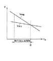
すなわち、定電圧Vregと発振停止電圧Vstoの温度特性が異なる場合、例えば、定電圧|Vreg|の方が温度に対して負の傾きが絶対値で大きい場合についての、定電圧|Vreg|と発振停止電圧|Vsto|に関する温度と電圧の関係を図13に示す。図13においては、横軸を温度、縦軸を電圧とし、定電圧Vreg,発振停止電圧Vstoについてのグラフを夫々示す。前記発振動作を確保するためには、動作保証温度範囲における高温時、すなわち、図13に示すB点においても、|Vreg|>|Vsto|を確保しなければならない。ここで、前記B点における温度は、例えば、一般に公知の腕時計の耐熱温度である。
【0026】
よって、他の低い温度領域では、定電圧|Vreg|値を必要以上に高くしなければならなくなる。つまり、従来の定電圧発生回路および水晶発振回路においては、無駄な電力を消費していることになる。したがって、低消費電力化のためには、定電圧Vregと発振停止電圧Vstoの温度特性を同様にすることが有効であることが分かる。すなわち、従来は定電圧Vregと発振停止電圧Vstoの温度勾配の差が大きくなり、高温側(あるいは低温側)の発振動作を保証するために、前記|Vreg|>|Vsto|を常に成り立たせなければならず、低温側(あるいは高温側)では、|Vreg|を発振動作を保証する以上に高くしなければならないので、結果として無駄な電力を消費していた。
【0027】
しかし、前記発振停止電圧Vstoは、水晶発振回路内の発振用インバータINV0を構成するPMOSQP0の閾値電圧Vthp0およびNMOSQN0の閾値電圧Vthn0に依存しており、前述したような従来の発振用インバータにおいては、定電圧発生回路において形成される定電圧Vregのみを調整することで低消費電力化を図ることしかできなかった。
【0028】
すなわち、発振用インバータを構成するトランジスタの形成において閾値電圧を変更させてしまうと、発振用インバータとしての特性も変わってしまうため、発振特性の変更に伴って様々な点での変更が必要となり、設計を困難にしてしまうこととなっていた。したがって、定電圧Vregと発振停止電圧Vstoにおける|Vreg|>|Vsto|の関係を保ちつつ、前記定電圧|Vreg|をできるだけ低くする、ということは困難であり、発振回路のさらなる低消費電力化が図れなかった。
【0029】
【発明が解決しようとする課題】
そこで、本発明は、上述したような問題を鑑みてなされたものであり、その目的は、発振用インバータを含む発振回路、半導体装置、携帯用の電子機器および時計において、発振回路を構成する発振用インバータにおけるトランジスタの閾値電圧を調整することにより低消費電力駆動且つ安定発振を行なうことにある。
【0030】
【0031】
【課題を解決するための手段】
(1)本発明の発振回路は、
異なる閾値電圧を有するトランジスタを用いて構成された複数の発振用インバータを含み、いずれか1つの発振用インバータが選択使用される発振用インバータ群と、
前記発振用インバータ群の出力側と入力側に接続された水晶振動子を有し、前記発振用インバータ群の出力信号を位相反転して、前記発振用インバータ群にフィードバック入力するフィードバック回路と、
を含むことを特徴とする。
【0032】
したがって、前記(1)の発明に係る発振回路によれば、前記発振用インバータ群のうち、前記発振用インバータのトランジスタ出力を最適な電圧に調整することができ、水晶発振回路としての発振出力を最適な状態にすることができ、低消費電力化が図れる。
【0033】
(2)本発明の発振回路は、前記(1)に記載の特徴点に加え、
前記発振用インバータ群から、いずれか1つの発振用インバータを選択する選択回路を含むことを特徴とする。
【0034】
したがって、前記(2)の発明に係る発振回路によれば、前記選択回路により最適な閾値電圧を有する発振用インバータを選択することができる。
【0035】
(3)本発明の発振回路は、前記(2)に記載の特徴点に加え、
前記発振回路は、テスト回路と同一の基板上に形成され、
前記水晶振動子を搭載していない状態で、前記テスト回路にて、前記各発振用インバータを選択し、該夫々の発振用インバータのショート電流を測定することにより、前記発振用インバータ群の中から1つの発振用インバータを特定し、前記選択回路にて前記発振用インバータを選択するものであることを特徴とする。
【0036】
したがって、前記(3)の発明に係る発振回路によれば、ICチップまたはウエハ上に形成された発振用インバータ群の夫々の発振用インバータのショート電流を測定することができるので、製造条件に係わらず最適な発振用インバータが得られ、歩留りを向上させることができるとともに、安定かつ低消費電力な発振特性を得ることができる。また、前記選択回路も前記テスト回路と前記同一基板上に形成することもできる。
【0037】
(4)本発明の発振回路は、前記(3)に記載の特徴点に加え、
前記テスト回路は、テスト用パッドと接続され、前記テスト用パッドへの印加電圧が制御されることによって、前記テスト回路を介して、前記各発振用インバータを選択することを特徴とする。
【0038】
したがって、前記(4)の発明に係る発振回路によれば、前記テスト用パッドへの印加電圧の組み合わせにより、前記テスト回路により、前記各発振用インバータを選択する信号を形成することができ、夫々の発振用インバータのショート電流を測定することができる。
【0039】
(5)本発明の発振回路は、前記(1)〜(4)のいずれかに記載の特徴点に加え、
前記選択回路は、前記発振用インバータと対応して設けられ、かつ複数のパッドと接続された、複数の単位回路を含み、
前記複数の単位回路は、夫々フューズ,不揮発性メモリ,記憶素子のうちのいずれか1つを含み、前記パッドへ電圧を印加することにより、前記発振用インバータを選択することを特徴とする。
【0040】
したがって、前記(5)の発明に係る発振回路によれば、フューズ,不揮発性メモリ,記憶素子のうちのいずれか1つを含む手段を付加することにより、容易に前記発振用インバータを選択する選択回路を構成することができる。
【0041】
(6)本発明の発振回路は、前記(1)〜(5)のいずれかに記載の特徴点に加え、
前記発振用インバータ群は、第1の閾値電圧を有するトランジスタを含んで構成された第1の発振用インバータと、前記第1の閾値電圧とは異なる第2の閾値電圧を有するトランジスタを含んで構成された第2の発振用インバータと、前記第1及び第2の閾値電圧とは異なる第3の閾値電圧を有するトランジスタを含んで構成された第3の発振用インバータとを少なくとも含むことを特徴とする。
【0042】
したがって、前記(6)の発明に係る発振回路によれば、前記発振用インバータ群における閾値電圧の差が微小であるトランジスタを含む3つの発振用インバータのうち、前記発振用インバータに流れるソースドレイン電流を最適な電流に調整することができ、水晶発振回路としての発振出力を最適な状態にすることができ、低消費電力化が図れる。
【0043】
(7)本発明の発振回路は、前記(1)〜(5)に記載の特徴点に加え、
前記各発振用インバータの電源ラインは、第1の電位側と、前記第1の電位とは電位の異なる第2の電位側に接続され、
前記発振回路は、前記第1の電位と前記第2の電位による電位差をもって、振幅を行なうものであることを特徴とする。
【0044】
したがって、前記(7)の発明に係る発振回路によれば、前記発振用インバータの振幅を前記第1の電源と、前記定電圧との間で行なうことができるため、前記電圧振幅に基づいた安定かつ低消費電力な発振特性を得ることができる。
【0045】
(8)本発明の発振回路は、前記(7)に記載の特徴点に加え、
前記第1の電位と前記第2の電位による電位差は、前記発振用インバータの発振停止電圧の絶対値よりも大きいものであることを特徴とする。
【0046】
したがって、前記(8)の発明に係る発振回路によれば、前記発振用インバータにより安定な発振動作を確保することができる。
【0047】
(9)本発明の発振回路は、前記(7)または(8)に記載の特徴点に加え、
選択する発振用インバータに流れるショート電流が、選択する発振用インバータを構成するトランジスタのオン電流よりも大きいという条件を満たす範囲で、前記発振用インバータの選択を行なうと共に、
前記第1の電位と前記第2の電位による電位差を、最小の電圧とすることを特徴とする。
【0048】
したがって、前記(9)の発明に係る発振回路によれば、前記発振用インバータにより安定かつ低消費電力な発振動作を行なうことができ、低電源電圧化にも対応することができる。
【0049】
(10)本発明の定電圧発生回路は、
一端側が第1の電位側、他端側が定電圧出力側に接続され、閾値電圧が夫々異なる複数のトランジスタを含み、いずれか1つのトランジスタが選択使用される定電圧制御回路と、
前記定電圧制御回路の参照電圧が一方の端子への入力され、他方の端子へ所与の基準電圧が入力されたオペアンプと、
一端が前記定電圧制御回路の前記各トランジスタの他端側に接続され、他端側が第2の電位側に接続され、前記オペアンプの出力を受けてゲート入力電圧が制御されるトランジスタと、
を含むことを特徴とする。
【0050】
したがって、前記(10)の発明に係る定電圧発生回路によれば、ICチップ上に形成されたトランジスタ群の夫々のトランジスタ選択時における定電圧の値をモニタ端子にて測定することができるので、製造条件に係わらず、最適な定電圧が得られ、ほぼ同一のチップ面積にて、低消費電力な定電圧を得ることができる。
【0051】
(11)本発明の定電圧発生回路は、前記(10)に記載の特徴点に加え、
前記定電圧発生回路は、前記定電圧制御回路における複数のトランジスタから1つのトランジスタを選択する選択回路を含むことを特徴とする。
【0052】
したがって、前記(11)の発明に係る定電圧発生回路によれば、前記選択回路により、前記最適なトランジスタを選択することができる。
【0053】
(12)本発明の定電圧発生回路は、前記(11)に記載の特徴点に加え、
前記定電圧発生回路はモニタ端子と接続されるとともに、テスト回路と同一の基板上に設けられ、
検査工程において、前記テスト回路は、前記定電圧制御回路における各トランジスタを選択し、前記定電圧制御回路における各トランジスタによる出力電圧を前記モニタ端子にて夫々測定することにより、前記定電圧制御回路における複数のトランジスタの中から1つのトランジスタを特定し、前記選択回路にて、前記トランジスタを選択することを特徴とする。
【0054】
したがって、前記(12)の発明に係る定電圧発生回路によれば、ICチップ上に形成されたトランジスタ群の夫々のトランジスタ選択時における定電圧の値をモニタ端子にて測定することができるので、製造条件に係わらず、最適な定電圧が得られ、ほぼ同一のチップ面積にて、低消費電力な定電圧を得ることができる。
【0055】
(13)本発明の定電圧発生回路は、前記(12)に記載の特徴点に加え、
前記テスト回路は、テスト用パッドと接続され、前記テスト用パッドへの印加電圧が制御されることによって、前記テスト回路を介して、前記定電圧制御回路における各トランジスタを選択することを特徴とする。
【0056】
したがって、前記(13)の発明に係る定電圧発生回路によれば、前記テスト用パッドへの印加電圧の組み合わせにより、前記テスト回路により、前記定電圧制御回路の各トランジスタを選択する信号を形成することができ、前記夫々のトランジスタにより形成される前記参照電圧を測定することができる。
【0057】
(14)本発明の定電圧発生回路は、前記(10)乃至(13)のうちのいずれかに記載の特徴点に加え、
前記選択回路は、前記定電圧制御回路における前記複数のトランジスタと対応して形成され、かつ複数のパッドと接続された、複数の単位回路を含み、
前記複数の単位回路は、夫々フューズ,不揮発性メモリ,記憶素子のうちのいずれか1つを含み、前記パッドへ電圧を印加することにより、前記トランジスタを選択することを特徴とする。
【0058】
したがって、前記(14)の発明に係る定電圧発生回路によれば、フューズ,不揮発性メモリ,記憶素子のうちのいずれか1つを含む手段を付加することにより、容易に前記発振用インバータを選択する選択回路を構成することができる。
【0059】
(15)本発明の定電圧発生回路は、前記(10)乃至(14)のいずれかに記載の特徴点に加え、
前記定電圧制御回路は、第4の閾値電圧を有するトランジスタと、前記第4の閾値電圧とは異なる第5の閾値電圧を有するトランジスタと、前記第4及び第5の閾値電圧とは異なる第6の閾値電圧を有するトランジスタとを少なくとも含み、各前記トランジスタは一端側が第1の電位側に接続され、他端側が定電圧出力側に接続されていることを特徴とする。
【0060】
したがって、前記(15)の発明に係る定電圧発生回路によれば、ICチップ上に形成されたテスト回路内の閾値電圧の異なる3種類のトランジスタによる定電圧値をモニタ端子にて測定することができるので、最適なトランジスタを選択することができ、製造条件に係わらず、最適な定電圧が得られ、ほぼ同一のチップ面積にて、低消費電力な定電圧を得ることができる。
【0061】
(16)本発明の定電圧発生回路は、前記(10)乃至(15)のうちのいずれかに記載の特徴点に加え、
前記定電圧発生回路の出力電圧を、発振回路へ供給することを特徴とする。
【0062】
したがって、前記(16)の発明に係る定電圧発生回路によれば、前記発振回路の発振特性に応じて前記定電圧を調整することができるので、前記発振回路へ最適な定電圧を供給することができる。
【0063】
(17)本発明の半導体装置は、
発振回路と、定電圧発生回路と、テスト回路とを含む半導体装置であって、
前記発振回路は、
異なる閾値電圧を有するトランジスタを用いて構成された複数の発振用インバータを含み、いずれか1つの発振用インバータが選択使用される発振用インバータ群と、
前記発振用インバータ群における複数の発振用インバータから1つの発振用インバータを選択する第1の選択回路と、
外付けされた水晶振動子と出力側及び入力側が接続された前記発振用インバータ群の出力信号を位相反転して、前記発振用インバータ群にフィードバック入力するフィードバック回路と、
を含み、
前記定電圧発生回路は、
一端側が第1の電位側、他端側が定電圧出力側に接続され、閾値電圧が夫々異なる複数のトランジスタを含み、いずれか1つのトランジスタが選択使用される定電圧制御回路と、
前記定電圧制御回路の参照電圧が一方の端子へ入力され、他方の端子へ所与の基準電圧が入力されたオペアンプと、
一端が前記定電圧制御回路の前記各トランジスタの他端側に接続され、他端側が第2の電位側に接続され、前記オペアンプ出力を受けてゲート入力電圧が制御されるトランジスタと、
前記定電圧制御回路における複数のトランジスタから1つのトランジスタを選択する第2の選択回路と、
を含み、
前記テスト回路は、前記発振回路および前記定電圧発生回路と夫々接続されるとともに、
前記定電圧発生回路の出力電圧をモニタするモニタ端子と、テスト用パッドと接続されて設けられ、
検査工程において、前記モニタ端子に電圧を印加した状態で、前記テスト用パッドへの印加電圧を制御することにより、前記テスト回路を介して前記各発振用インバータを夫々選択して、前記各発振用インバータのショート電流を夫々測定し、
前記ショート電流測定後に、前記テスト用パッドへの印加電圧を制御することにより、前記テスト回路を介して前記定電圧制御回路における各トランジスタを夫々選択して、前記各トランジスタの出力電圧を前記モニタ端子にて夫々測定し、
前記発振用インバータの発振動作を確保できる範囲で、前記発振回路内の前記発振用インバータを前記第1の選択回路にて選択するとともに、前記定電圧発生回路内の定電圧制御回路におけるトランジスタを前記第2の選択回路にて選択することを特徴とする。
【0064】
したがって、前記(17)の発明に係る半導体装置によれば、前記水晶発振回路の発振用インバータのショート電流測定結果と、定電圧の測定結果とによる組み合わせの中から最適なショート電流と定電圧の組み合わせを選択することができ、半導体装置における発振回路の安定発振出力を得ることができると共に、歩留りを向上することができ、一層の低消費電力化を図ることができる。
【0065】
(18)本発明の携帯用電子機器は、
前記(1)乃至(9)のいずれかの発振回路を含み、前記発振回路の発振出力から動作基準信号を形成することを特徴とする。
【0066】
したがって、前記(18)の発明に係る携帯用電子機器によれば、携帯用電子機器の製造ばらつきによらず、発振用インバータの動作マージンを確保しつつ、電子回路の低消費電力化が図れ、携帯用電子機器において、発振動作を安定して行なうことができるだけでなく、使用電池の長寿命化を図ることができ、携帯用電子機器の使い勝手を向上することができる。
【0067】
(19)本発明の携帯用電子機器は、前記(18)に記載の特徴点に加え、
前記発振回路への供給電圧を形成する前記(10)乃至(16)のいずれかの定電圧発生回路を含むことを特徴とする。
【0068】
したがって、前記(19)の発明に係る携帯用電子機器によれば、さらに、最小の定電圧を前記発振回路に供給することができるため、電子回路の低消費電力化が図れる。
【0069】
(20)本発明の時計は、前記(19)に記載の特徴点に加え、
前記(1)乃至(9)のいずれかの発振回路を含み、前記発振回路の発振出力から時計基準信号を形成することを特徴とする。
【0070】
したがって、前記(20)の発明に係る時計によれば、時計の製造ばらつきによらず、発振用インバータの動作マージンを確保しつつ、時計において、発振動作を安定して行なうことができるだけでなく、使用電池の長寿命化を図ることができ、時計の使い勝手を向上することができる。
【0071】
(21)本発明の時計は、前記(20)に記載の特徴点に加え、
前記発振回路への供給電圧を形成する前記(10)乃至(16)のいずれかの定電圧発生回路を含むことを特徴とする。
【0072】
したがって、前記(21)の発明に係る時計によれば、さらに、最小の定電圧を前記発振回路に供給することができるため、時計回路の低消費電力化が図れる。
【0073】
【発明の実施の形態】
次に、本発明の好適な実施の形態を図面に基づき詳細に説明する。
【0074】
<実施の形態1>
図2には、本発明の好適な実施の形態1にかかる定電圧発生回路および水晶発振回路が示されている。本実施の形態の水晶発振回路は、クォーツタイプの腕時計に使用される水晶発振回路である。尚、前記図11に示される回路と対応する部材には、同一符号を付し、その説明は省略する。
【0075】
本実施の形態の水晶発振回路は、複数の発振用インバータユニットにより発振用インバータ群を形成し、かつ前記発振用インバータユニットを構成するPMOS/NMOSの各閾値電圧を、各発振用インバータユニットごとに異なるように形成し、最適な発振用インバータユニットを選択することができるようにしたものである。
【0076】
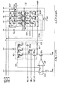
図2に示される水晶発振回路について説明する。本実施の形態の水晶発振回路は、発振用インバータ群10と、選択制御回路20P,20Nと、水晶振動子X’talと、フィードバック回路を構成する高抵抗Rfとを含んで構成されている。ここで、MOSは半導体基板上に形成されているICチップに形成されたものであり、他の素子はプリント基板上に前記ICチップと接続されて実装されたものである。前記フィードバック回路は、抵抗Rf以外に、位相補償用のコンデンサCD,CGを含んで構成され、発振用インバータ群10のドレイン出力を、180度位相反転されたゲート入力として発振用インバータ群10の初段の発振用インバータユニットINV1のゲートへフィードバック入力するものである。
【0077】
前記発振用インバータ群10においては、PMOSQP4とNMOSQN4を含む第1の発振用インバータユニットINV1、PMOSQP5とNMOSQN5を含む第2の発振用インバータユニットINV2,PMOSQP6とNMOSQN6を含む第3の発振用インバータユニットINV3が形成されている。
【0078】
そして各発振用インバータユニットINV1〜3は、それぞれ第1の電位側とこれよりも低い電圧の第2の電位側に接続され、両電位の電位差により電力供給を受け駆動されるように構成されている。ここで、本実施の形態の水晶発振回路においては、前記第1の電位は接地電圧Vddに設定され、第2の電位は定電圧発生回路から供給される負の定電圧Vregに設定されている。
【0079】
これらの発振用インバータ群10を構成する、発振用インバータユニットINV1〜3における夫々のトランジスタは、前記各発振用インバータユニットごとにそれぞれ異なる閾値電圧にて形成されているものである。たとえば、NMOSQN4,QN5,QN6の各閾値電圧は、Vthn4>Vthn5>Vthn6とされ、前記各NMOSの閾値電圧の大きさに対応して、PMOSQP4,QP5,QP6の閾値電圧は、|Vthp4|>|Vthp5|>|Vthp6|となるように形成されている。そして、この閾値電圧の制御については、トランジスタ形成時の不純物の打ち込み濃度を制御することにより、夫々の発振用インバータユニットごとに閾値電圧が異なるように形成される。そして、たとえば、これらの閾値電圧の差としては前記Vthn4とVthn5,Vthn5とVthn6、Vthp4とVthp5,Vthp5とVthp6との各電位差を約0.1V程度にすることができる。
【0080】
そして、前記各発振用インバータユニットINV1〜3は、一端に接地電圧Vddが印加された前記コンデンサCGの他端と、夫々の入力ゲートが共通に電気的に接続される。さらに、前記各発振用インバータユニットINV1〜3は、各出力ノードが共通に接続されるとともに、接地電圧Vddが一端に印加されたコンデンサCDの他端、および水晶振動子X’talの一端と接続される。また、前記水晶振動子X’talの他端は、前記コンデンサCGの他端、各発振用インバータユニットINV1〜3のゲート入力、フィードバック抵抗Rfの一端と接続されている。更に、前記フィードバック抵抗Rfの他端は各発振用インバータユニットINV1〜3の各出力部と接続されており、前記各発振用インバータユニットINV1〜3の出力は、各ゲートにフィードバックされている。
【0081】
更に、前記各発振用インバータユニットINV1〜3は、選択信号が入力されるNMOS選択制御回路20N及びPMOS選択制御回路20P間に接続されて設けられている。前記NMOS選択制御回路20Nはゲートに選択信号を受けるNMOSQN7〜QN9により構成されるとともに、前記PMOS選択制御回路20Pは、ゲートに選択信号を受けるCMOSインバータ回路IP1〜IP3と、その出力を各ゲートにて受けるPMOSQP7〜QP9により構成されている。すなわち、前記PMOS選択制御回路20Pを構成するPMOSQP7〜QP9の各ゲートには前記各選択信号の反転信号が入力されるものである。
【0082】
そして、前記PMOS選択制御回路20P、前記NMOS選択制御回路20N、発振用インバータ群10の接続について、たとえば、発振用インバータユニットINV1を例として以下に説明する。尚、発振用インバータユニットINV2,INV3についても全く同じ構成であるものとする。
【0083】
前記PMOS選択制御回路20Pに含まれるPMOSQP7は、ソースに電源電圧Vssが印加されるとともに、ドレインがPMOSQP4のソースと接続されている。そして、前記NMOS選択制御回路20Nに含まれるNMOSQN7は、ソースに定電圧Vregが印加されるとともに、ドレインがNMOSQN4のソースと接続されている。そして、前記選択制御用NMOSQN7のゲートには、発振用インバータ群10における発振用インバータユニットINV1の選択/非選択を命令する選択信号SEL1が入力され、前記選択制御用PMOSQP7のゲートには、選択信号SEL1の反転信号が印加されている。すなわち、前記選択信号SEL1はハイレベルで発振用インバータユニットINV1を選択状態、ロウレベルで前記発振用インバータユニットINV1を非選択状態にすることができる。
【0084】
以上、発振用インバータユニットINV1を例として説明したが、前述したように発振用インバータユニットINV2,INV3の構成も同様であって、発振用インバータユニットINV2においては、ゲートに選択信号SEL2が入力される選択制御用PMOSQP8と、ゲートに選択信号SEL2の反転信号が入力される選択制御用NMOSQN8が設けられている。また、同様に、インバータINV3においては、ゲートに選択信号SEL3が入力される選択制御用NMOSQN9と、ゲートに選択信号SEL1の反転信号が入力される選択制御用PMOSQP9が同様に設けられている。
【0085】
このように、夫々閾値電圧の異なる前記発振用インバータユニットINV1〜3により構成された発振用インバータ群10および選択制御回路20P,20Nは、水晶発振回路としての発振出力を最適な状態にするために、前記発振用インバータ群10のうち、前記発振用インバータユニットのトランジスタ出力を最適な電圧に調整するために設けられたものである。
【0086】
すなわち、前記選択信号SEL1〜3の選択制御回路20P,20Nへの入力により、前記発振用インバータユニットINV1〜3の起動を制御し、最適な閾値電圧にて形成されたトランジスタを有する発振用インバータユニットを選択するものである。この選択信号SEL1〜3の電圧レベルの切り替え方法および回路については、後に図3を用いて詳細に説明する。
【0087】
次に、本実施の形態の水晶発振回路における、発振用インバータユニットの選択方法について説明する。本実施の形態では、たとえば、発振用インバータユニットINV1を選択する場合について説明する。
【0088】
選択信号SEL1がハイレベルとされ、選択制御用PMOSQP7のゲートにロウレベル、NMOSQN7のゲートにハイレベルの電圧が印加されるため、前記PMOSQP7とNMOSQN7はオンする。したがって、発振用インバータユニットINV1において、PMOSQP4のソースが接地電圧Vdd、NMOSQN4のソースが定電圧Vregと、それぞれ電気的に接続されることにより、発振用インバータユニットINV1を選択することができる。
【0089】
一方、選択信号SEL1,SEL2はロウレベルとされるので、選択制御用PMOSQP8,QP9のゲートにはそれぞれ選択信号SEL1,SEL2の反転信号、すなわちハイレベルの信号が印加されるので、PMOSQP8,QP9はオフする。そして、選択制御用NMOSQN8,QN9のゲートには前記選択信号SEL1,SEL2すなわちロウレベルの信号が印加されるので、NMOSQN8,QN9はオフする。よって、発振用インバータユニットINV3,INV4は両電源と電気的に切り離され選択されない。
【0090】
次に、前記選択信号SEL1〜3の形成方法について、図3を用いて説明する。
【0091】
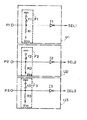
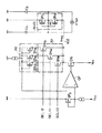
図3に本発明の好適な実施の形態1にかかる発振用インバータユニット選択回路が示されている。本実施の形態の発振用インバータユニット選択回路は、水晶発振回路において、前記発振用インバータユニットINV1〜3により構成される発振用インバータ群10のうち、最適な発振用インバータユニットを選択する選択信号SEL1〜3を形成するための回路である。
【0092】
発振用インバータユニット選択回路は、前記発振用インバータユニットの数分の単位回路により構成され、たとえば、図2に示すような3種類の発振用インバータユニットINV1〜3を有する水晶発振回路用には、3つの単位回路U1〜U3が設けられている。すなわち、前記発振用インバータユニット選択回路は、3種類のパッドP1〜P3及び3種類のフューズ回路F1〜F3を含む。前記フューズ回路F1〜F3は、それぞれ一端が接地電圧Vddと接続され、他端がパッドP1〜P3と接続されたフューズf1〜f3と、一端が電源電圧Vssと接続され、他端がパッド及び前記フューズf1〜f3の他端と直列に接続された抵抗R1〜R3と、出力インバータI1〜I3とを含んで構成されている。
【0093】
そして、たとえば、単位回路U1が選択信号SEL1形成用の回路である場合には、前記単位回路U1の出力が、発振用インバータユニットINV1のNMOSQN7のゲート、または水晶発振回路内の選択制御回路20Pにおけるインバータを介してPMOSQP7のゲートに入力される。
【0094】
本実施の形態の発振用インバータユニット選択回路において、フューズ回路F1〜F3のフューズf1〜f3はたとえば20V程度の高電圧を印加することによって切断することができる。たとえば、発振用インバータユニットINV1を選択する場合は、まず、パッドP1に高電圧を印加して、フューズf1を切断することによって、電流をパッドP1から抵抗R1を介して電源Vssに向かって流すようにする。このことによって、出力インバータINVU1に入力される電圧はロウレベルとなり、前記出力インバータINVU1の出力電圧、すなわち発振用インバータユニット選択回路における単位回路U1の出力信号はハイレベルとなる。したがって、図3に示される選択信号SEL1はハイレベルとされて選択制御用NMOSQN7がオンし、選択制御用PMOSQP7がオフする。
【0095】
以上、発振用インバータユニットINV1を選択する場合について説明したが、INV2,INV3の選択も同様に行なうことができる。たとえば、発振用インバータユニットINV2を選択する場合は、パッドP2に高電圧を印加して、単位回路U2のフューズf2を切断し、発振用インバータユニットINV3を選択する場合は、パッドP3に高電圧を印加して、単位回路U3のフューズf3を切断することで同様にして所望の発振用インバータユニットを選択することができる。ここで、本実施の形態では、フューズの切断による情報記憶の方法を例として説明したが、これに限定されることなく、不揮発性メモリや記憶素子等を用いて情報を記憶させることもできる。
【0096】
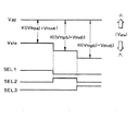
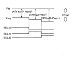
ここで、図4に発振停止電圧Vstoと選択信号SEL1〜3の関係についてのタイミングチャートを示す。図4において、横軸は時間を表わしている。ここで、発振停止電圧Vstoと、接地電圧Vddとにおいては、差電圧が大きくなるほど発振停止電圧|Vsto|が大きくなるものである。
【0097】
まず、選択信号SEL1がハイレベルとされることにより、前記した式1により発振停止電圧|Vsto|は、K(|Vth p7|+Vthn7)(K:定数)となる。そして、前記選択信号SEL1がロウレベル,選択信号SEL2がハイレベルとされることによって、発振停止電圧|Vsto|は、K(|Vthp8|+Vthn8)となる。また、前記選択信号SEL2がロウレベル,選択信号SEL3がハイレベルとされることによって、発振停止電圧|Vsto|は、K(|Vthp9|+Vthn9)となる。つまり、SEL1がハイレベルにされたときの発振停止電圧|Vsto|が最も低く、SEL3がハイレベルにされたときに発振停止電圧|Vsto|が最も高くなる。
【0098】
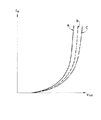
ところで、発振用インバータユニット選択回路におけるフューズの切断は、ICの検査時に行なわれ、このときに、まず、発振用インバータ群10と接続された選択制御回路20NのNMOSQN7〜QN9の夫々のソースが共通に接続された、定電圧発生回路の出力電圧である負の定電圧Vregの値と、発振用インバータユニットINV1〜3の夫々に流れるショート電流Isの測定により発振用インバータユニットの選択が行なわれる。
【0099】
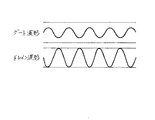
図5(a)は発振用インバータユニットに流れるショート電流Isの測定方法を示す図、図5(b)は、縦軸を発振停止電圧|Vsto|、横軸をショート電流Isとして表わした、発振停止電圧|Vsto|とショート電流Isとの関係を示すグラフである。
【0100】
発振用インバータユニットのショート電流の測定は、図に示すように、発振用インバータユニットを構成するPMOSQPSのソースに接地電圧Vddを印加し、NMOSQNSのソースに定電圧Vregを印加し、前記PMOSQPs,前記NMOSQNsの共通ゲートと共通ドレインをショートさせて、接地電圧Vdd−定電圧Vreg間に流れる電流を測定することにより行なわれる。
【0101】
このとき、発振停止電圧|Vsto|と発振用インバータユニットのショート電流Isの関係のグラフにおいて、水晶発振回路の低消費電力化のためには、前述した定電圧Vreg,発振停止電圧Vstoは、|Vreg|>|Vsto|かつ|Vreg|をできるだけ低くするという条件を満たさなければならない。
【0102】
すなわち、前記ショート電流Isについては、前記PMOSQPSのオン電圧以上、つまり閾値電圧|VthpS|以上、かつ最も低い定電圧|Vreg|となるように発振用インバータユニットおよび定電圧Vregを選択する必要がある。更に、発振停止電圧|Vsto|においては、要求される発振電圧がNMOSQNSのオン電圧以下、つまり閾値電圧VthnS以下の電圧を選択する必要がある。したがって、低消費電力化のためには、図に示す領域1の範囲内でのショート電流Isおよび発振停止電圧|Vsto|である必要がある。一方、この条件を満たしつつ、近年の電源の低電圧化に対応できる発振用インバータユニットを選択するために、トランジスタのオンオフ動作が補償される範囲で安定発振する、最も低いショート電流の発振用インバータユニットを選択することが必要となる。すなわち、前述したショート電流測定の結果にしたがって、この条件を満たす最適の発振用インバータユニットを選択することで、水晶発振回路の低消費電力化を実現するものである。
【0103】
このために、ICの検査工程において、特に図示しないテスト回路および前記テスト回路と接続されたテスト用パッドを使用して、水晶振動子X’talの基板への実装前に、各発振用インバータユニットINV1〜3においてショート電流Isを測定し、オンオフ動作が補償される範囲で最も低いショート電流のものを特定する。このときICテストはウエハの状態で行ない、夫々のICチップ内に設けられたテスト回路およびテスト用パッドを使用して、それぞれのICチップについてショート電流の測定が行なわれる。また、このとき、発振用インバータ群10および選択制御回路20P,20Nのみをアクティブとし、他の素子は非アクティブ状態にしてテストが行なわれる。
【0104】
ところで、前記テスト用パッドは発振用インバータユニットの数およびテスト回路の論理に応じて、1つまたは複数設けられると共に、前記テスト回路には、前記テスト用パッドへの入力信号の電圧レベルの組み合わせによって、前記選択信号SEL1〜3のうちのいずれか1つをハイレベルにする論理回路を含む回路が形成されているものである。そして、ショート電流の測定は、前記テスト回路において、擬似的に、各発振用インバータユニットへ前記ハイレベルの選択信号を夫々入力した状態で行なわれる。このとき、前記出力ライン102と接続されたモニタ用パッドMPを利用して、定電圧と同等の負の電圧Vregを印加することにより、前記発振用インバータ群に接地電圧Vddと、定電圧Vre gを印加する。
【0105】
そして、ショート電流Is測定後に、発振用インバータ群10のうちの最適な発振用インバータユニットを特定し、前記発振用インバータユニットに対応して設けられた、発振用インバータユニット選択回路の単位回路におけるフューズを切断し、最適な発振用インバータユニットを1つ選択する。
【0106】
以上述べたように、本実施の形態の水晶発振回路は、発振用インバータユニットのショート電流IsをIC検査時にテストすることができるため、製造条件に係わらず、最適な発振用インバータが得られ、歩留りを向上させることができるとともに、安定かつ低消費電力な発振特性を得ることができる。
【0107】
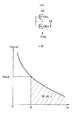
ここで、このようにして得られた本実施の形態の発振用インバータにおける発振動作についてのグラフを図6に示し、発振動作について説明する。図6において、横軸を時間を示し、ドレイン波形とゲート波形の時間軸を共通として示す。最適な発振用インバータユニットが選択された水晶発振回路において、前記発振用インバータユニットの最適な駆動能力に応じてゲート入力波形の振幅が増幅される。そして、前記ゲート入力波形に対してドレイン出力波形は位相が180度反転される。そして、ドレイン容量CDは、高調波成分をカットし、発振周波数成分だけを有効にして、水晶発振回路の高調波発振を防ぐフィルターの役目を果たしている。そして、前記抵抗Rf,ドレイン容量CD,水晶振動子X’tal,ゲート容量CGを含むフィードバック回路はドレイン波形の位相を180度変換させるものである。
【0108】
このように、本実施の形態の水晶発振回路における発振用インバータの出力特性は、最適の発振用インバータユニットにて発振動作が行なわれているため、出力特性が良く低消費電力な発振回路を実現することができる。
【0109】
以上本実施の形態の水晶発振回路について説明してきたが、本実施の形態においては、異なる閾値電圧を有する発振用インバータユニットを3種類であるとして説明したが、発振用インバータユニットの数は特に限定されることなく自由に設定することができ、同様に発振用インバータユニット選択回路の数も発振用インバータユニットの数と対応させて設けることができる。
【0110】
本実施の形態においては、閾値電圧の設定を発振用インバータINV1>INV2>INV3、すなわち、Vthn4>Vthn5>Vthn6,|Vthp4|>|Vthp5|>|Vthp6|として記載したが、これに限定されることなく、閾値電圧の設定をINV1<INV2<INV3、すなわち、Vthn4<Vthn5<Vthn6,|Vthp4|<|Vthp5|<|Vthp6|として設定することもできる。
【0111】
<実施の形態2>
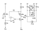
次に、図7を用いて本実施の形態の定電圧発生回路について説明する。
【0112】
本実施の形態の定電圧発生回路は、オペアンプの一方の入力電圧を制御するNMOSを複数かつ夫々異なる閾値電圧にて形成し、前記複数のNMOSのうち最適なNMOSを選択することができるようにしたものである。
【0113】
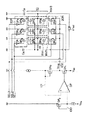
本実施の形態の定電圧発生回路は、オペアンプOPと、選択制御回路30と、出力ゲートNMOSQN1と、定電圧制御回路40と、−入力用PMOSQP2とを含んで構成されている。
【0114】
前記オペアンプOPは、+入力端子と−入力端子とを有し、+入力端子は定電圧制御回路40により形成される電圧を受ける。また、前記−入力端子はPMOSにより構成され、接地電圧Vddと定電流源の間に設けられた前記選択制御用PMOSQP2により制御される電圧を受ける。そして、前記オペアンプOPは、前記+入力端子に印加された電圧と、−入力端子に印加された電圧との電位差を増幅して出力する。また、前記−入力用PMOSQP2は、ソースには接地電圧Vssが印加され、ゲートとドレインが共通に接続され、かつ定電流源と接続されている。
【0115】
前記出力ゲートNMOSQN1は、前記オペアンプOPの出力をゲートに受けるものであって、且つ、ドレインが定電圧発生回路の出力ライン102と接続されている。また、前記出力ゲートNMOSQN1のソースには電源電圧Vssが印加されている。
【0116】
前記定電圧制御回路40は、NMOSQN10〜QN12を含んで構成されている。この定電圧制御回路40は、定電圧発生回路にて形成される定電圧Vregを、前記オペアンプOPの+入力端子の入力電圧を制御することによって制御するための回路であって、第1の電位と、前記第1の電位よりも低い第2の電位の間に設けられた前記NMOSQN10〜QN13の夫々のゲートとドレインが共通にオペアンプOPの−入力端子に接続されている。すなわち、前記NMOSQN10〜QN12の各ドレイン及びゲートはオペアンプOPの+入力端子と接続されているとともに、ソースが選択制御回路30を介して定電圧発生回路の出力ライン102に電気的に接続されている。
【0117】
ここで、前記定電圧制御用NMOSQN10〜QN12は、夫々異なる閾値電圧にて形成されており、前記NMOSQN10の閾値電圧Vthn10,前記NMOSQN11の閾値電圧Vthn11,前記NMOSQN12の閾値電圧Vthn12は、たとえば、Vthn10>Vthn11>Vthn12の関係となるように形成されている。そして、この閾値電圧の制御については、トランジスタ形成時の不純物の打ち込み濃度を制御することにより形成することができる。このとき、たとえば、Vthn10とVthn11,Vthn11とVthn12との各電位差は0.1V程度にすることができる。
【0118】
そして、前述したように、選択制御回路30が、前記定電圧制御回路40と接続されて設けられている。すなわち、前記定電圧制御用NMOSQN10〜QN12の夫々のドレインと直列に接続されて、各ゲートにて選択信号を受ける選択制御用NMOSQN13〜QN15が夫々対応して設けられている。前記選択制御用NMOSQN13〜QN15は、夫々のソースが共通に定電圧発生回路の出力ライン102と接続されており、前記出力ライン102の電位が実質的に定電圧発生回路の出力電圧Vregとなるものである。
【0119】
そして、前記選択信号は、実施の形態1の水晶発振回路の例と同様に、異なる閾値電圧を有する定電圧制御回路を構成するNMOSのうちの1つを選択するための信号であり、選択信号SEL10がハイレベルでNMOSQN10を選択状態、SEL11がハイレベルでNMOSQN11を選択状態、SEL12がハイレベルでNMOSQN12を選択状態とすることができる。また、前記選択信号SEL10〜12が夫々ロウレベルで前記NMOSQN10〜QN12を夫々非選択状態とすることができる。
【0120】
前記定電圧制御回路40を構成する夫々閾値電圧の異なるNMOSQN10〜QN12は、定電圧発生回路により形成された定電圧Vregを最適な状態で形成するために、前記定電圧制御回路40のうちの1つのNMOSに電流を流すことにより、オペアンプOPの+入力端子への印加電圧すなわち−入力端子への印加電圧との差電圧を選択することができ、前記オペアンプOPの出力信号すなわち定電圧Vregを制御することを可能とするものである。
【0121】
すなわち、前記選択信号SEL10〜12の選択制御回路30への入力により、前記定電圧制御回路40を構成するNMOSQN13〜QN15のオンオフを制御し、最適な閾値電圧にて形成されたNMOSを1つ選択するものである。この選択信号SEL10〜SEL12の電圧レベルの切り替え方法及び回路については、図3に示す回路と同様のものを使用し、同様の切り替え方法により選択信号SEL10〜12を形成することができるのでここでは説明は省略する。
【0122】
次に、本実施の形態の定電圧発生回路における、定電圧制御回路の選択方法について説明する。本実施の形態では、たとえば、NMOSQN10を選択する場合について説明する。
【0123】
選択信号SEL10がハイレベルとされ、選択制御用NMOSQN13のゲートにハイレベルの電圧が印加されるため、前記NMOSQN13はオンする。したがって、定電圧制御回路40において、NMOSQN10のソースがオン状態のNMOSQN1を介して電源電圧Vssと電気的に接続されることにより、定電圧制御用NMOSQN10を選択することができる。
【0124】
一方、選択信号SEL11,SEL12は共にロウレベルとされるので、選択制御用NMOSQN14,QN15のゲートには前記選択信号SEL11,SEL12すなわちロウレベルの信号が印加されるので、NMOSQN14,QN15はオフする。よって、定電圧制御用NMOSQN11,QN12は両電源と電気的に切り離され選択されない。
【0125】
ここで、図8に定電圧Vregと選択信号SEL10〜12の関係についてのタイミングチャートを示す。図8において、横軸は時間を表わしている。ここで、定電圧|Vreg|と、接地電圧Vddとにおいては、差電圧が大きくなるほど定電圧|Vreg|が大きくなるものである。
【0126】
まず、選択信号SEL10がハイレベルとされることにより、前述したように、定電圧は、|Vreg|=α(|Vthp2|+Vthn)(α:定数)で表わすことができるので、定電圧|Vreg|はα(|Vthp2|+Vthn10)となる。そして、前記選択信号SEL10がロウレベル,選択信号SEL11がハイレベルとされることによって、定電圧|Vreg|はα(|Vthp2|+Vthn11)となる。また、前記選択信号SEL11がロウレベル,選択信号SEL12がハイレベルとされることによって、定電圧|Vreg|はα(|Vthp2|+Vthn12)となる。つまり、SEL10がハイレベルにされたときの定電圧|Vreg|が最も低く、SEL3がハイレベルにされたときに定電圧|Vreg|が最も高くなる。
【0127】
ところで、前記したように、定電圧制御回路40に含まれるNMOSの選択は、図3に示す回路と同様の選択信号形成回路により、ICの検査工程においてフューズを切断することにより行なわれる。また、実施の形態1と同様に、前記選択信号形成回路において、フューズの切断による情報記憶方法でなくとも、不揮発性メモリや記憶素子等を用いて情報を記憶させることもできる。
【0128】
前記定電圧制御回路に含まれるNMOSの選択においては、実施の形態1でも述べたように、定電圧Vreg,発振停止電圧Vstoは、|Vreg|>|Vsto|かつ|Vreg|を低くするという両方の条件を満たさなければならない。前述したように、前記発振停止電圧Vstoは、発振用インバータを構成するトランジスタのNMOSQN0,PMOSQP0の閾値電圧Vthn0,|Vthp0|に依存するため、特に図示しないテスト回路と接続されたテスト用パッドに印加する電圧レベルを制御して、選択信号SEL10,SEL11,SEL12を順にハイレベルとする。ここで、テスト回路は、実施の形態1に記載した前記テスト回路と同様に、前記テスト用パッドへの入力信号の組み合わせにより、選択信号SEL10〜12を選択的に形成する論理回路を含む回路であり、前記テスト用パッドは1つまたは複数設けることができる。
【0129】
そして、定電圧制御用NMOSQN10〜QN12を順にオンさせて、定電圧Vregを変化させ、出力ライン102に接続されたモニタ用パッドMPにて定電圧Vregを測定する。このとき、ICテストはウエハの状態で行ない、夫々のICチップ内に設けられた前記テスト回路,前記テスト用パッドおよびモニタ用パッドを使用して夫々のICチップについて定電圧Vregの測定が行なわれる。また、測定時には、定電圧制御回路40,選択制御回路30のみがアクティブとされ、他の素子は非アクティブ状態とされているものである。
【0130】
そして、実施の形態1に記載したように、水晶発振回路における発振用インバータにおいてショート電流Isを測定し、前記した関係を満たす最適な定電圧Vregを特定する。そして、ICチップの実効領域に形成された定電圧発生回路において定電圧制御回路40に含まれる、前記特定した最適なNMOSと接続された選択信号形成回路のフューズの切断を行ない、定電圧制御用NMOSを1つ選択する。
【0131】
以上、本実施の形態の定電圧発生回路について説明してきたが、前述したように、本実施の形態の定電圧発生回路は、動作マージンを確保しつつできるだけ低い定電圧|Vreg|を形成することを特徴とするものであるので、トランジスタ数をさほど増加させることなく実現することができるため、チップ面積を大きく増加させることなく、最適な定電圧が設定でき、低消費電力な定電圧Vregを得ることができる。
【0132】
本実施の形態においては、異なる閾値電圧を有する定電圧制御用NMOSを3種類であるとして説明したが、この数は特に限定されることなく自由に設定することができ、同様に定電圧選択回路の単位回路の数も定電圧制御用NMOSの数と対応させて設けることができる。
【0133】
本実施の形態においては、閾値電圧の設定を定電圧制御用NMOSQN10>QN11>QN12、すなわち、Vthn10>Vthn11>Vthn12として記載したが、これに限定されることなく、閾値電圧の設定をQN10<QN11<QN12、すなわち、Vthn10<Vthn11<Vthn12として設定することもできる。
【0134】
また、実施の形態1,実施の形態2として、水晶発振回路の発振用インバータにて最適発振用インバータを選択できるもの、定電圧発生回路の定電圧制御回路の最適NMOSを選択できるものとして別々に例を挙げて説明したが、図1に示されるように、同時に実施の形態1の定電圧発生回路と、実施の形態2の水晶発振回路を適用することもでき、この場合最も低消費電力化が図れることはいうまでもない。この場合、前記選択信号SEL1〜3を形成する第1の選択信号形成回路と、前記選択信号SEL10〜12を形成する第2の選択信号形成回路が必要となるが、前記モニタ用パッドは共用することができる。また、前述したように、前記第1の選択信号形成回路と第2の選択信号形成回路の回路構成は同一にすることもできる。そして、図1のように構成した場合、水晶発振回路の発振用インバータのショート電流測定結果と、定電圧Vregの測定結果とによる組み合わせの中から最適な組み合わせを選択することができ、安定した発振特性を確保しつつ、歩留りを向上させることができ、さらに一層の低消費電力化を図ることができる。
【0135】
以上、実施の形態1,2を用いて本発明の水晶発振回路、定電圧発生回路、発振用インバータユニット選択回路、選択信号形成回路について述べてきたが、前記発振用インバータユニット選択回路、選択信号形成回路は図示した回路構成に限定されることなく様々な回路構成にて実現することができ、例えば、フューズの切断は高電圧の印加でなくとも、レーザーにてポリシリコンにて形成されたフューズを切断することもできる。
【0136】
<実施の形態3>
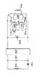
次に、図9に腕時計に用いられる電子回路の一例が示されている。
【0137】
この腕時計は、図示しない発電機構を内蔵している。使用者が腕時計を装着し腕を動かすと、発電機構の回転錘が回転し、そのときの運動エネルギーにより発電ロータが高速回転され、発電ステータス側に設けられた発電コイル300から交流電圧が出力される。
【0138】
この交流電圧が、ダイオード302で整流され、二次電池301を充電する。この二次電池301は、昇圧回路303および補助コンデンサ304と共に主電源を構成する。
【0139】
本実施の形態では、二次電池の電圧が低くて時計の駆動電圧に満たないときには、昇圧回路303により二次電池の電圧を時計駆動可能な高電圧に変換し、補助コンデンサ304に蓄電する。そして、この補助コンデンサ304の電圧を電源として時計回路が動作する。
【0140】
この時計回路は、実施の形態1,2に記載した発振回路と定電圧発生回路を含む半導体装置として構成されており、この半導体装置に端子を介して接続された水晶振動子X’talを用いて予め設定された発振周波数、ここで32768Hzの周波数の発振出力を生成し、この発振出力を分周することにより、一秒ごとに極性の異なる駆動パルスを出力するように構成されている。この駆動パルスは、時計回路に接続されたステップモータの駆動コイル306へ入力される。これにより、図示しないステップモータは、駆動パルスが通電されるごとにロータを回転駆動し、図示しない時計の秒針、分針、時針を駆動し、時刻を表示板にアナログ表示することになる。
【0141】
ここで、本実施の形態の時計回路330は、前述した主電源から供給される電圧により駆動される電源電圧回路部220と、この電源電圧からこの値よりも低い所定の一定電圧Vregを生成する実施の形態2に記載した定電圧発生回路210と、この定電圧Vregにより駆動される定電圧動作回路部240とを含んで構成される。
【0142】
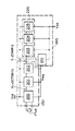
図10には、前記時計回路330のより詳細な機能ブロック図が示されている。
【0143】
定電圧動作回路部240は、外部接続された水晶振動子X’talを一部に含んで構成された実施の形態1に記載した水晶発振回路200と、波形整形ゲート201と、高周波分周回路202とを含んで構成される。
【0144】
前記電源電圧回路部220は、レベルシフタ203と、中低周波分周回路204と、その他の回路205とを含んで構成される。なお、本実施の形態の時計回路では、前記電源電圧回路部220と、定電圧発生回路210とは、主電源から供給される電圧により駆動される電源電圧動作回路部240を構成している。
【0145】
前記水晶発振回路200は、水晶振動子X’talを用いて基準周波数fs=32768Hzの正弦波出力を波形整形ゲート201に出力する。
【0146】
前記波形整形ゲート201は、この正弦波出力を矩形波に整形した後、高周波分周回路202へ出力する。
【0147】
前記高周波分周回路202は、基準周波数32768Hzを2048Hzまで分周し、その分周出力をレベルシフタ203を介して中低周波数分周回路204へ出力する。
【0148】
前記中低周波数分周回路204は、2048Hzまで分周された信号を、さらに1Hzまで分周し、その他の回路205へ入力する。
【0149】
前記その他の回路205は、1Hzの分周信号に同期してコイルを通電駆動するドライバ回路を含んで構成され、この1Hzの分周信号に同期して時計用駆動用ステップモータを駆動する。
【0150】
本実施の形態の時計回路において、主電源から供給される電源電圧Vssにより回路全体が駆動される電源電圧動作回路部240以外に、これにより低い定電圧Vregで駆動される定電圧動作回路部220を設けたのは以下の理由による。
【0151】
すなわち、このような時計回路では、長期間安定した動作を確保するために、その消費電力を低減することが必要となる。
【0152】
通常、回路の消費電力は、信号の周波数、回路の容量に比例し、さらに供給電源電圧の二乗に比例して増大する。
【0153】
ここで、時計回路に着目してみると、回路全体の消費電力を低減するためには、回路各部に供給する電源電圧を低い値、たとえばVre gに設定すれば良い。この定電圧発生回路210は、実施の形態2に記載したように、前記水晶発振回路200の発振動作を補償する範囲で最小の定電圧Vregを形成することができる。
【0154】
次に、信号周波数に着目してみると、時計回路は、信号周波数が高い水晶発振回路200、波形整形ゲート201、高周波分周回路202と、それ以外の回路205とに大別することができる。この信号の周波数は、前述したように回路の消費電力と比例関係がある。
【0155】
そこで、本実施の形態の定電圧発生回路210は、主電源から供給される電源電圧Vssから、それより低い定電圧Vregを生成し、これを高周波信号を扱う回路部230、すなわち水晶発振回路200、波形整形ゲート201、高周波分周回路202へ供給している。このように、前記高周波信号を扱う回路230に対して供給する駆動電圧を低くすることにより、定電圧発生回路210の負担をさほど増加させることなく、時計回路全体の消費電力を効果的に低減することができる。
【0156】
なお、本実施の形態において、高周波分周回路202と中低周波分周回路204との間にレベルシフタ203を設けたのは、以下の理由による。
【0157】
高周波分周回路202の出力波高値は、定電圧Vregレベルであり、主電源の電圧Vssの波高値より小さい。このため、前記電源電圧Vssで駆動されている中低周波分周回路204に、高周波分周回路202の定電圧Vregレベルの出力をそのまま入力しても、この入力値が中低周波分周回路202の初段のロジックレベルの電圧を超えないため、中低周波分周回路204が正常に動作しない。よって、前記中低周波分周回路204が正常に動作するように、前記レベルシフタ203を使い、前記高周波分周回路202の出力波高値を定電圧レベルから電源電圧レベルまで引き上げている。
【0158】
以上述べたように、本実施の形態の時計回路およびこれを含む電子回路は、実施の形態1の水晶発振回路、実施の形態2の定電圧発生回路を含んでいるために、製造ばらつきによらず、発振用インバータの動作がマージンを確保しつつ、最小の定電圧を前記水晶発振回路に供給することができるため、電子回路、時計回路の低消費電力化が図れる。したがって、前述したような、時計または携帯用の電子機器において、発振動作を安定して行なうことができるだけでなく、使用電池の長寿命化を図ることができ、時計又は携帯用の電子機器の使い勝手を向上することができる。
【0159】
【図面の簡単な説明】
【図1】本発明による実施の形態2の定電圧発生回路及び実施の形態1の水晶発振回路を有する発振回路の概略図である。
【図2】本発明による実施の形態1の水晶発振回路を有する発振回路の概略図である。
【図3】本発明による実施の形態1の発振用インバータ選択回路の概略図である。
【図4】本発明による実施の形態1の発振停止電圧と選択信号の関係を示すタイミングチャートの概略図である。
【図5】本発明による発振用インバータのショート電流を測定する方法について説明するための図と、発振停止電圧とショート電流との関係を示すグラフである。
【図6】本発明による実施の形態1の水晶発振回路のゲート波形と,ドレイン波形を示す概略図である。
【図7】本発明による実施の形態2の定電圧発生回路を有する発振回路の概略図である。
【図8】本発明による実施の形態2の定電圧と選択信号の関係を示すタイミングチャートの概略図である。
【図9】本発明による実施の形態3の時計の機能ブロック図である。
【図10】本発明による実施の形態3の携帯用電子機器の機能ブロック図である。
【図11】本発明による従来の定電圧発生回路及び水晶発振回路を有する発振回路の概略図である。
【図12】従来の定電圧発生回路における定電流源と接続されたNMOSに流れる定電流とゲート−ソース間電圧との関係を示すグラフである。
【図13】定電圧|Vreg|と発振停止電圧|Vsto|に関する温度と電圧の関係を示す図である。
【符号の説明】
10・・・発振用インバータ群
20P,20N・・・選択制御回路(水晶発振回路)
30・・・選択制御回路(定電圧発生回路)
40・・・定電圧制御回路
INV1〜3・・・発振用インバータユニット
P1〜P3・・・パッド
OP・・・オペアンプ
Rf・・・帰還抵抗
CG,CD・・・補償用コンデンサ
X’tal・・・水晶振動子
U1〜U4・・・単位回路
F1〜F3・・・フューズ回路
f1〜f3・・・フューズ
R1〜R3・・・抵抗
I1〜I3・・・出力インバータ
200・・・水晶発振回路
201・・・波形整形用ゲート
202・・・高周波分周回路
203・・・レベルシフタ
204・・・中低周波分周回路
205・・・その他回路
210・・・定電圧発生回路
220・・・電源電圧回路部
230・・・定電圧駆動動作回路部
240・・・電源電圧動作回路
300・・・発電コイル
301・・・二次電池
302・・・ダイオード
303・・・昇圧回路
304・・・補助コンデンサ
306・・・時計用モータコイル[0001]
TECHNICAL FIELD OF THE INVENTION
The present invention provides an oscillation circuit,HalfConductor devices and portable electronic devices and watches equipped with themSekiI do.
[0002]
[Background Art]
2. Description of the Related Art Conventionally, an oscillation circuit using a crystal oscillator has been widely used in watches, portable telephones, computer terminals, and the like. In such a portable electronic device or watch, it is necessary to save power consumption and extend the life of the battery.
[0003]
From the viewpoint of saving power consumption, the present inventor analyzed the power consumption of an electronic circuit used in a portable electronic device, particularly a wristwatch. From this analysis, it has been confirmed that, among the electronic circuits formed on the printed circuit board, in the semiconductor device, the power consumption of the oscillation circuit portion occupies a larger proportion than other circuit portions. That is, it has been found that reducing power consumption in an oscillation circuit portion of an electronic circuit used in a portable electronic device is effective in extending the life of a battery used.
[0004]
FIG. 11 shows an example of a conventional crystal oscillation circuit and a constant voltage generation circuit.
[0005]
This crystal oscillation circuit includes a crystal resonator X'tal, an oscillation inverter INV0, and a high resistance Rf forming a feedback circuit. The feedback circuit includes a capacitor C for phase compensation in addition to the resistor Rf.D, CG, And the feedback output of the drain output of the oscillation inverter INV0 to the gate of the oscillation inverter INV0 as a 180 ° phase-inverted gate input.
[0006]
Conventionally, an oscillation inverter INV0 used in such a crystal oscillation circuit includes a pair of P-type field effect transistors (hereinafter, referred to as PMOS) QP.0, N-type field effect transistor (hereinafter referred to as NMOS) QN0And each PMOS QP0, NMOS QN0, And the drain functions as an output side. And each of the transistors QP0, QN0Have their drain sides connected to each other, and their source sides connected to the ground voltage Vdd side and the negative constant voltage Vreg side, respectively.
[0007]
In the crystal oscillation circuit having the above configuration, when the constant voltage Vreg is applied to the oscillation inverter INV0, the output of the oscillation inverter INV0 is inverted by 180 degrees and fed back to the gate. Thereby, the PMOS QP constituting the oscillation inverter INV00, NMOS QN0Are alternately turned on and off, the oscillation output of the crystal oscillation circuit gradually increases, and finally the crystal resonator X'tal performs a stable oscillation operation.
[0008]
However, in the conventional crystal oscillation circuit, the PMOS QP is always used both at startup and after stable oscillation.0, NMOS QN0Since both transistors are turned on and off alternately, there is a problem described below.
[0009]
In the conventional crystal oscillation circuit, PMOSQP0, NMOS QN0Are alternately turned on and off. In this case, the PMOSQP0Is turned on, most of the energy charged in the crystal unit X'tal is discharged as it is. Therefore, in the next charging cycle, the crystal unit X'tal must be charged from the beginning, and the present inventor has found that this charging is a major problem in reducing the power consumption of the entire circuit. Was.
[0010]
In other words, in a state where the crystal oscillation circuit is oscillating stably, a stable oscillation state can be maintained without completely discharging the power charged in the crystal resonator X'tal in the charge / discharge cycle. . However, in the conventional circuit, in this charge / discharge cycle, the cycle of discharging the charge power of the crystal unit X'tal as it is and repeating the charge is repeated, which is a major factor in increasing the power consumption of the entire circuit. I was
[0011]
In such a crystal oscillation circuit, the absolute value of the oscillation stop voltage | Vsto |0Threshold voltage of Vthn0, QP of the PMOS0Assuming that the threshold voltage is Vthp0, it can be expressed as in
[0012]
Equation 1: | Vsto | = K · (| Vthp0 | + Vthn0)
Here, the constant K is 0.8 to 0.9, and | Vthp0 | indicates the absolute value of Vthp0. As described above, the oscillation stop voltage Vsto depends on the threshold voltage Vthn0 of the NMOS transistor and the threshold voltage Vthp0 of the PMOS.
[0013]
On the other hand, the constant voltage generation circuit includes an operational amplifier OP and a negative (hereinafter referred to as “-”) input voltage control PMOS QP.2And plus (hereinafter referred to as +) NMOS QN for input voltage control2, Output NMOS QN1It is comprised including. That is, the negative input terminal of the operational amplifier OP is connected to a PMOS QP having a gate connected to the drain and provided between the constant current source and the power supply voltage Vss.2Connected to the drain of Further, the + input terminal of the operational amplifier OP has an NMOS QN having a gate short-circuited to the drain and provided between the constant current source and the power supply voltage Vss.2Connected to the drain.
[0014]
And the NMOS QN2Output NMOS QN, in which the source and the drain thereof are connected in series, the output of the operational amplifier OP is received at the gate, and the source is connected to the power supply voltage Vss.1Is provided. Therefore, the output voltage of the operational amplifier OP, that is, the output voltage Vreg of the constant voltage generation circuit is equal to the PMOS QP2And NMOS QN2Are affected by the respective threshold voltages Vthp2 and Vthn2.
[0015]
That is, the operation of this circuit will be described below.2The constant current flows through the PMOS QP to the signal line 100.2│Vthp2│ (α: constant) depending on the threshold voltage | Vthp2 | Then, the operational amplifier OP and the NMOS QN1As a result, the
[0016]
Therefore, the output voltage of the operational amplifier OP, that is, the output voltage Vreg of the constant voltage generation circuit is equal to the PMOS QP2Threshold voltage Vthp2 and NMOS QN2Of the threshold voltage Vthn2. That is, the constant voltage | Vreg | is proportional to | Vthp2 | + Vthn2. Therefore, the conventional crystal oscillation circuit operates using the constant voltage value Vreg depending on | Vthp2 | + Vthn2 as a power supply.
[0017]
Therefore, in the conventional constant voltage generating circuit, even when the values of threshold voltages Vthp2 and Vthn2 vary in the semiconductor manufacturing process and | Vthp2 | or Vthn2 increases, the constant voltage | Vreg | also increases. Therefore, there is an advantage that | Vreg |> | Vsto | is always maintained in the relationship between the constant voltage Vreg and the oscillation stop voltage Vsto, the oscillation operation can be secured, and the yield of the IC can be improved.
[0018]
Conventionally, in order to operate the oscillator with low power consumption, the number of constant current sources for operating the constant voltage generating circuit has been reduced as much as possible within a range where the constant voltage generating circuit can operate. However, with the need for the development of portable devices as described above, in order to reduce the power consumption of the oscillating inverter, the oscillation operation must be ensured (| Vreg |> | Vsto |) while the constant voltage | It has become necessary to lower Vreg | as much as possible. However, when the constant current from the constant current source that operates the constant voltage generating circuit is reduced, the change in the constant voltage Vreg when the constant current fluctuates due to a temperature change.
[0019]
Here, the temperature characteristics of the transistor will be described with reference to the constant voltage generation circuit illustrated in FIG. In this constant voltage generation circuit, the NMOS QN2, PMOSQP2The current values of the constant current sources TA and TB that operate the LED have temperature dependence. That is, when the constant current sources TA and TB are composed of, for example, a depletion type PMOS, the constant current ID can be expressed by the following equation (2). Here, the current amplification factor of the depletion PMOS constituting the constant current source is β, the absolute value of the threshold voltage is | Vth |, and the gate-source voltage is VGSAnd
[0020]
Equation 2: ID= 1/2 · β · (VGS− | Vth |)2
Here, since the gate of the depletion PMOS is short-circuited in order to form a constant current, the VGS becomes 0V.
[0021]
Equation 3: ID= 1/2 · β · (-Vth)2
As shown in Equation 3, the constant current IDDoes not depend on the power supply voltage. Therefore, the constant current IDIs proportional to the square of the temperature-dependent current amplification factor β and the threshold voltage Vth.DAlso varies with temperature changes.
[0022]
FIG. 12 shows the NMOS QN23 is a graph showing the temperature fluctuation of FIG. In FIG. 12, the vertical axis represents the constant current I.DWhere the horizontal axis represents the gate-source voltage VGSRepresents In the graph, three types of curves are shown.2, The curve C shows the case where the threshold voltage is high, and the curve B shows the case where the threshold voltage is between A and C. Although not shown, the PMOS QP2Have similar characteristics. That is, as can be seen from this graph, the variation of the constant voltage Vreg with respect to the temperature change is the variation of the constant current value and the NMOS QN2Threshold voltage Vthn2, PMOS QP2Of the absolute value of the threshold voltage Vthp2.
[0023]
On the other hand, as for the variation of the oscillation stop voltage Vsto with respect to the temperature, since the oscillation stop voltage Vsto depends on the above-described
[0024]
Therefore, the temperature coefficient of the constant voltage Vreg is the change amount of the constant current source and the change amount of the threshold voltage (| Vthp2 | + Vthn2), whereas the temperature coefficient of the oscillation stop voltage Vsto is the threshold voltage (| Vthp0 | + Vthn0). ), The temperature coefficient, that is, the temperature characteristic is different.
[0025]
That is, when the temperature characteristics of the constant voltage Vreg and the oscillation stop voltage Vsto are different, for example, when the constant voltage | Vreg | FIG. 13 shows the relationship between the temperature and the voltage with respect to the stop voltage | Vsto |. FIG. 13 is a graph showing the constant voltage Vreg and the oscillation stop voltage Vsto, with the horizontal axis representing temperature and the vertical axis representing voltage. In order to ensure the oscillation operation, | Vreg |> | Vsto | must be ensured at a high temperature in the operation guarantee temperature range, that is, also at the point B shown in FIG. Here, the temperature at the point B is, for example, a heat-resistant temperature of a generally known wristwatch.
[0026]
Therefore, in other low temperature regions, the constant voltage | Vreg | value must be increased more than necessary. That is, in the conventional constant voltage generation circuit and the conventional crystal oscillation circuit, useless power is consumed. Therefore, it can be seen that it is effective to make the temperature characteristics of the constant voltage Vreg and the oscillation stop voltage Vsto the same in order to reduce the power consumption. That is, conventionally, the difference in temperature gradient between the constant voltage Vreg and the oscillation stop voltage Vsto becomes large, and the above-mentioned | Vreg |> | Vsto | On the low-temperature side (or high-temperature side), | Vreg | must be set higher than that required for guaranteeing the oscillation operation. As a result, wasteful power is consumed.
[0027]
However, the oscillation stop voltage Vsto is equal to the PMOS QP which constitutes the oscillation inverter INV0 in the crystal oscillation circuit.0Threshold voltage Vthp0 and NMOS QN0In the conventional oscillation inverter as described above, only the constant voltage Vreg formed in the constant voltage generating circuit can be adjusted to reduce the power consumption. .
[0028]
That is, if the threshold voltage is changed in the formation of the transistor that constitutes the oscillation inverter, the characteristics of the oscillation inverter also change, so that it is necessary to make changes at various points along with the change in the oscillation characteristics. This would make the design difficult. Therefore, it is difficult to keep the constant voltage | Vreg | as low as possible while maintaining the relationship of | Vreg |> | Vsto | in the constant voltage Vreg and the oscillation stop voltage Vsto, and further reduce the power consumption of the oscillation circuit. Could not be planned.
[0029]
[Problems to be solved by the invention]
Therefore, the present invention has been made in view of the above-described problems, and an object thereof is to provide an oscillation circuit including an oscillation inverter,HalfIn a conductor device, a portable electronic device, and a timepiece, low power consumption driving and stable oscillation are performed by adjusting a threshold voltage of a transistor in an oscillation inverter included in an oscillation circuit.
[0030]
[0031]
[Means for Solving the Problems]
(1) The present inventionThe oscillation circuit of
An oscillation inverter group including a plurality of oscillation inverters configured using transistors having different threshold voltages, and any one of the oscillation inverters is selectively used;
A feedback circuit that has a crystal oscillator connected to the output side and the input side of the oscillation inverter group, inverts the phase of the output signal of the oscillation inverter group, and feeds back the oscillation inverter group to a feedback circuit;
It is characterized by including.
[0032]
Therefore,According to the invention of the above (1)According to the oscillation circuit, of the oscillation inverter group, the transistor output of the oscillation inverter can be adjusted to an optimum voltage, and the oscillation output of the crystal oscillation circuit can be set to the optimum state. Power consumption can be reduced.
[0033]
(2) The present inventionThe oscillation circuit ofThe above (1)In addition to the features described in
A selection circuit for selecting any one of the oscillation inverters from the oscillation inverter group is included.
[0034]
Therefore,According to the invention of the above (2)According to the oscillation circuit, an oscillation inverter having an optimum threshold voltage can be selected by the selection circuit.
[0035]
(3) The present inventionThe oscillation circuit ofThe above (2)In addition to the features described in
The oscillation circuit is formed on the same substrate as the test circuit,
In a state where the crystal oscillator is not mounted, the test circuit selects each of the oscillation inverters, and measures the short-circuit current of each of the oscillation inverters. One oscillation inverter is specified, and the selection circuit selects the oscillation inverter.
[0036]
Therefore,According to the invention of the above (3)According to the oscillation circuit, the short-circuit current of each oscillation inverter of the oscillation inverter group formed on the IC chip or the wafer can be measured, so that an optimal oscillation inverter can be obtained regardless of the manufacturing conditions. The yield can be improved, and oscillation characteristics with stable and low power consumption can be obtained. Further, the selection circuit may be formed on the same substrate as the test circuit.
[0037]
(4) The present inventionThe oscillation circuit ofThe above (3)In addition to the features described in
The test circuit is connected to a test pad and controls each of the oscillation inverters via the test circuit by controlling a voltage applied to the test pad.
[0038]
Therefore,According to the invention of the above (4)According to the oscillation circuit, a signal for selecting each of the oscillation inverters can be formed by the test circuit by a combination of voltages applied to the test pads, and the short-circuit current of each oscillation inverter is measured. be able to.
[0039]
(5) The present inventionThe oscillation circuit ofThe above (1) to (4)In addition to the features described in any of
The selection circuit is provided corresponding to the oscillation inverter, and is connected to a plurality of pads, includes a plurality of unit circuits,
The plurality of unit circuits each include any one of a fuse, a nonvolatile memory, and a storage element, and select the oscillation inverter by applying a voltage to the pad.
[0040]
Therefore,According to the invention of the above (5).According to the oscillation circuit, a selection circuit for easily selecting the oscillation inverter can be configured by adding a means including any one of a fuse, a nonvolatile memory, and a storage element.
[0041]
(6) The present inventionThe oscillation circuit ofThe above (1) to (5)In addition to the features described in any of
The oscillation inverter group includes a first oscillation inverter including a transistor having a first threshold voltage, and a transistor having a second threshold voltage different from the first threshold voltage. A second oscillation inverter, and a third oscillation inverter including a transistor having a third threshold voltage different from the first and second threshold voltages. I do.
[0042]
Therefore,According to the invention of the above (6).According to the oscillation circuit, the source / drain current flowing through the oscillation inverter can be adjusted to an optimum current among the three oscillation inverters including the transistor having a small difference in threshold voltage in the oscillation inverter group. In addition, the oscillation output of the crystal oscillation circuit can be set to an optimum state, and low power consumption can be achieved.
[0043]
(7) The present inventionThe oscillation circuit ofThe above (1) to (5)In addition to the features described in
A power supply line of each of the oscillation inverters is connected to a first potential side and a second potential side different in potential from the first potential,
The oscillation circuit is configured to perform amplitude by a potential difference between the first potential and the second potential.
[0044]
Therefore,According to the invention of (7) aboveAccording to the oscillation circuit, since the amplitude of the oscillation inverter can be adjusted between the first power supply and the constant voltage, it is possible to obtain stable and low power consumption oscillation characteristics based on the voltage amplitude. Can be.
[0045]
(8) The present inventionThe oscillation circuit ofThe above (7)In addition to the features described in
A potential difference between the first potential and the second potential is larger than an absolute value of an oscillation stop voltage of the oscillation inverter.
[0046]
Therefore,According to the invention of (8) aboveAccording to the oscillation circuit, a stable oscillation operation can be ensured by the oscillation inverter.
[0047]
(9) The present inventionThe oscillation circuit of(7) or (8) aboveIn addition to the features described in
While the short-circuit current flowing to the selected oscillation inverter satisfies the condition that the ON current of the transistor constituting the selected oscillation inverter is larger, the selection of the oscillation inverter is performed,
A difference between the first potential and the second potential is set to a minimum voltage.
[0048]
Therefore,According to the invention of the above (9).According to the oscillation circuit, a stable and low power consumption oscillation operation can be performed by the oscillation inverter, and it is possible to cope with a low power supply voltage.
[0049]
(10) The present inventionThe constant voltage generation circuit of
A constant voltage control circuit having one end connected to the first potential side, the other end connected to the constant voltage output side, including a plurality of transistors having different threshold voltages, and one of the transistors being selectively used;
An operational amplifier in which a reference voltage of the constant voltage control circuit is input to one terminal and a given reference voltage is input to the other terminal;
A transistor having one end connected to the other end of each of the transistors of the constant voltage control circuit, the other end connected to the second potential side, and receiving an output of the operational amplifier to control a gate input voltage;
It is characterized by including.
[0050]
Therefore,According to the invention of the above (10).According to the constant voltage generating circuit, the value of the constant voltage at the time of selecting each transistor of the transistor group formed on the IC chip can be measured at the monitor terminal. And a constant voltage with low power consumption can be obtained in almost the same chip area.
[0051]
(11) The present inventionThe constant voltage generation circuit ofThe above (10)In addition to the features described in
The constant voltage generation circuit includes a selection circuit that selects one transistor from a plurality of transistors in the constant voltage control circuit.
[0052]
Therefore,According to the invention of (11) aboveAccording to the constant voltage generation circuit, the optimum transistor can be selected by the selection circuit.
[0053]
(12) The present inventionThe constant voltage generation circuit ofThe above (11)In addition to the features described in
The constant voltage generation circuit is connected to a monitor terminal, and is provided on the same substrate as the test circuit.
In the inspection step, the test circuit selects each transistor in the constant voltage control circuit, and measures the output voltage of each transistor in the constant voltage control circuit at the monitor terminal, whereby the test circuit controls the constant voltage control circuit. One transistor is specified from a plurality of transistors, and the transistor is selected by the selection circuit.
[0054]
Therefore,According to the invention of (12) aboveAccording to the constant voltage generating circuit, the value of the constant voltage at the time of selecting each transistor of the transistor group formed on the IC chip can be measured at the monitor terminal. And a constant voltage with low power consumption can be obtained in almost the same chip area.
[0055]
(13) The present inventionThe constant voltage generation circuit ofThe above (12)In addition to the features described in
The test circuit is connected to a test pad and controls each voltage in the constant voltage control circuit via the test circuit by controlling a voltage applied to the test pad. .
[0056]
Therefore,According to the invention of the aforementioned (13).According to the constant voltage generation circuit, a signal for selecting each transistor of the constant voltage control circuit can be formed by the test circuit by a combination of voltages applied to the test pads. The measured reference voltage can be measured.
[0057]
(14) The present inventionThe constant voltage generation circuit ofThe above (10) to (13)In addition to the features described in any of the above,
The selection circuit includes a plurality of unit circuits formed corresponding to the plurality of transistors in the constant voltage control circuit and connected to a plurality of pads,
The plurality of unit circuits each include one of a fuse, a non-volatile memory, and a storage element, and select the transistor by applying a voltage to the pad.
[0058]
Therefore,According to the invention of the above (14).According to the constant voltage generating circuit, by adding a means including any one of a fuse, a nonvolatile memory, and a storage element, it is possible to easily configure a selecting circuit for selecting the oscillation inverter.
[0059]
(15) The present inventionThe constant voltage generation circuit ofThe above (10) to (14)In addition to the features described in any of
The constant voltage control circuit includes a transistor having a fourth threshold voltage, a transistor having a fifth threshold voltage different from the fourth threshold voltage, and a sixth transistor having a fourth threshold voltage different from the fourth and fifth threshold voltages. Wherein each of the transistors has one end connected to the first potential side and the other end connected to the constant voltage output side.
[0060]
Therefore,According to the invention of the above (15).According to the constant voltage generation circuit, the constant voltage value of three types of transistors having different threshold voltages in the test circuit formed on the IC chip can be measured at the monitor terminal. Thus, an optimum constant voltage can be obtained irrespective of manufacturing conditions, and a constant voltage with low power consumption can be obtained with almost the same chip area.
[0061]
(16) The present inventionThe constant voltage generation circuit ofThe above (10) to (15)In addition to the features described in any of the above,
An output voltage of the constant voltage generation circuit is supplied to an oscillation circuit.
[0062]
Therefore,According to the invention of the above (16).According to the constant voltage generation circuit, the constant voltage can be adjusted according to the oscillation characteristics of the oscillation circuit, so that an optimum constant voltage can be supplied to the oscillation circuit.
[0063]
(17) The present inventionThe semiconductor device of
An oscillation circuit, a constant voltage generation circuit, a semiconductor device including a test circuit,
The oscillation circuit includes:
An oscillation inverter group including a plurality of oscillation inverters configured using transistors having different threshold voltages, and any one of the oscillation inverters is selectively used;
A first selection circuit for selecting one oscillation inverter from a plurality of oscillation inverters in the oscillation inverter group;
A feedback circuit that inverts the phase of an output signal of the oscillation inverter group to which an external crystal oscillator and an output side and an input side are connected, and that performs feedback input to the oscillation inverter group;
Including
The constant voltage generating circuit,
A constant voltage control circuit having one end connected to the first potential side, the other end connected to the constant voltage output side, including a plurality of transistors having different threshold voltages, and one of the transistors being selectively used;
An operational amplifier in which a reference voltage of the constant voltage control circuit is input to one terminal and a given reference voltage is input to the other terminal;
A transistor having one end connected to the other end of each transistor of the constant voltage control circuit, the other end connected to the second potential side, and a gate input voltage controlled by receiving the output of the operational amplifier;
A second selection circuit that selects one transistor from a plurality of transistors in the constant voltage control circuit;
Including
The test circuit is connected to the oscillation circuit and the constant voltage generation circuit, respectively,
A monitor terminal for monitoring an output voltage of the constant voltage generating circuit, and a monitor terminal provided to be connected to the test pad;
In the inspection step, by controlling a voltage applied to the test pad while applying a voltage to the monitor terminal, each of the oscillation inverters is selected via the test circuit, and each of the oscillation inverters is selected. Measure the short-circuit current of each inverter,
After measuring the short-circuit current, by controlling the voltage applied to the test pad, each transistor in the constant voltage control circuit is selected via the test circuit, and the output voltage of each transistor is monitored by the monitor terminal. Measure each at
As long as the oscillation operation of the oscillation inverter can be ensured, the oscillation inverter in the oscillation circuit is selected by the first selection circuit, and the transistor in the constant voltage control circuit in the constant voltage generation circuit is The selection is performed by the second selection circuit.
[0064]
Therefore,According to the invention of the above (17).According to the semiconductor device, the optimum combination of the short-circuit current and the constant voltage can be selected from the combination of the measurement result of the short-circuit current of the oscillation inverter of the crystal oscillation circuit and the measurement result of the constant voltage. , A stable oscillation output of the oscillation circuit can be obtained, the yield can be improved, and the power consumption can be further reduced.
[0065]
(18) The present inventionPortable electronic devices
The above (1) to (9)Wherein the operation reference signal is formed from the oscillation output of the oscillation circuit.
[0066]
Therefore,According to the invention of the above (18).According to the portable electronic device, it is possible to reduce the power consumption of the electronic circuit while securing the operation margin of the oscillation inverter, regardless of the manufacturing variation of the portable electronic device, and to stabilize the oscillation operation in the portable electronic device. In addition to this, it is possible to extend the life of the battery used, and to improve the usability of the portable electronic device.
[0067]
(19) The present inventionPortable electronic devicesThe above (18)In addition to the features described in
Forming a supply voltage to the oscillation circuitThe above (10) to (16)Wherein the constant voltage generating circuit is provided.
[0068]
Therefore,According to the invention of the above (19),According to the portable electronic device, since the minimum constant voltage can be further supplied to the oscillation circuit, the power consumption of the electronic circuit can be reduced.
[0069]
(20) The present inventionThe clock is(19)In addition to the features described in
The above (1) to (9)And a clock reference signal is formed from an oscillation output of the oscillation circuit.
[0070]
Therefore,According to the invention of (20) aboveAccording to the timepiece, it is possible to stably perform the oscillating operation of the timepiece while securing the operation margin of the oscillation inverter irrespective of the manufacturing variation of the timepiece, and to extend the life of the battery used. It is possible to improve the usability of the watch.
[0071]
(21) The present inventionThe clock isThe above (20)In addition to the features described in
Forming a supply voltage to the oscillation circuitThe above (10) to (16)Wherein the constant voltage generating circuit is provided.
[0072]
Therefore,According to the invention of the above (21).According to the timepiece, the minimum constant voltage can be further supplied to the oscillation circuit, so that the power consumption of the timepiece circuit can be reduced.
[0073]
BEST MODE FOR CARRYING OUT THE INVENTION
Next, a preferred embodiment of the present invention will be described in detail with reference to the drawings.
[0074]
<
FIG. 2 shows a constant voltage generation circuit and a crystal oscillation circuit according to a preferred first embodiment of the present invention. The crystal oscillation circuit of the present embodiment is a crystal oscillation circuit used in a quartz wristwatch. The members corresponding to the circuit shown in FIG. 11 are denoted by the same reference numerals, and description thereof will be omitted.
[0075]
In the crystal oscillation circuit of the present embodiment, an oscillation inverter group is formed by a plurality of oscillation inverter units, and each threshold voltage of PMOS / NMOS constituting the oscillation inverter unit is set for each oscillation inverter unit. It is formed differently so that an optimum oscillation inverter unit can be selected.
[0076]
The crystal oscillation circuit shown in FIG. 2 will be described. The crystal oscillation circuit of the present embodiment includes an
[0077]
In the
[0078]
Each of the oscillation inverter units INV1 to INV1 to 3 is connected to a first potential side and a second potential side with a lower voltage, respectively, and is configured to be supplied with power and driven by a potential difference between the two potentials. I have. Here, in the crystal oscillation circuit of the present embodiment, the first potential is set to the ground voltage Vdd, and the second potential is set to the negative constant voltage Vreg supplied from the constant voltage generation circuit. .
[0079]
Each transistor in the oscillation inverter units INV1 to 3 constituting the
[0080]
Each of the oscillating inverter units INV1 to INV3 is connected to one end of the capacitor C to which the ground voltage Vdd is applied.GAnd the respective input gates are electrically connected in common. Further, each of the oscillation inverter units INV1 to INV1 to 3 has a capacitor C to which each output node is connected in common and a ground voltage Vdd is applied to one end.DAnd the other end of the crystal unit X'tal. The other end of the crystal unit X'tal is connected to the capacitor CG, The gate inputs of the oscillation inverter units INV1 to 3 and one end of the feedback resistor Rf. Further, the other end of the feedback resistor Rf is connected to each output section of each oscillation inverter unit INV1-3, and the output of each oscillation inverter unit INV1-3 is fed back to each gate.
[0081]
Further, each of the oscillation inverter units INV1 to 3 is provided so as to be connected between an NMOS
[0082]
The connection of the PMOS
[0083]
PMOS QP included in the PMOS
[0084]
Although the oscillation inverter unit INV1 has been described as an example, the configuration of the oscillation inverter units INV2 and INV3 is the same as described above, and the selection signal SEL2 is input to the gate of the oscillation inverter unit INV2. PMOS QP for selection control8And a selection control NMOS QN whose gate receives an inverted signal of the selection signal SEL2.8Is provided. Similarly, in the inverter INV3, the selection control NMOS QN whose selection signal SEL3 is input to the gate is provided.9And a selection control PMOS QP whose gate receives an inverted signal of the selection signal SEL1.9Are similarly provided.
[0085]
As described above, the
[0086]
That is, the input of the selection signals SEL1 to SEL3 to the
[0087]
Next, a method of selecting an oscillation inverter unit in the crystal oscillation circuit of the present embodiment will be described. In the present embodiment, for example, a case where the oscillation inverter unit INV1 is selected will be described.
[0088]
The selection signal SEL1 is set to the high level, and the selection control PMOS QP7Low level, NMOS QN7Since a high level voltage is applied to the gate of the PMOS QP7And NMOS QN7Turns on. Therefore, in the oscillation inverter unit INV1, the PMOS QP4Source is ground voltage Vdd, NMOS QN4Is electrically connected to the constant voltage Vreg, thereby selecting the oscillation inverter unit INV1.
[0089]
On the other hand, since the selection signals SEL1 and SEL2 are at the low level, the selection control PMOS QP8, QP9Are applied with inverted signals of the selection signals SEL1 and SEL2, that is, a high-level signal.8, QP9Turns off. Then, the selection control NMOS QN8, QN9Are applied with the selection signals SEL1 and SEL2, that is, a low-level signal.8, QN9Turns off. Therefore, the oscillation inverter units INV3 and INV4 are electrically disconnected from the two power supplies and are not selected.
[0090]
Next, a method of forming the selection signals SEL1 to SEL3 will be described with reference to FIG.
[0091]
FIG. 3 shows an oscillation inverter unit selection circuit according to a preferred first embodiment of the present invention. The oscillation inverter unit selection circuit according to the present embodiment includes a selection signal SEL1 for selecting an optimum oscillation inverter unit from the
[0092]
The oscillation inverter unit selection circuit is composed of unit circuits corresponding to the number of the oscillation inverter units. For example, for a crystal oscillation circuit having three types of oscillation inverter units INV1 to 3 shown in FIG. Three unit circuits U1 to U3 are provided. That is, the oscillation inverter unit selection circuit includes three types of pads P1 to P3 and three types of fuse circuits F1 to F3. Each of the fuse circuits F1 to F3 has one end connected to the ground voltage Vdd, the other end connected to the pads P1 to P3, the fuses f1 to f3, one end connected to the power supply voltage Vss, and the other end connected to the pad and the pad. It is configured to include resistors R1 to R3 connected in series with the other ends of the fuses f1 to f3, and output inverters I1 to I3.
[0093]
For example, when the unit circuit U1 is a circuit for forming the selection signal SEL1, the output of the unit circuit U1 is the NMOS QN of the oscillation inverter unit INV1.7Via the inverter of the
[0094]
In the oscillation inverter unit selection circuit of the present embodiment, fuses f1 to f3 of fuse circuits F1 to F3 can be cut by applying a high voltage of, for example, about 20V. For example, when the oscillation inverter unit INV1 is selected, first, a high voltage is applied to the pad P1 and the fuse f1 is cut off so that a current flows from the pad P1 to the power supply Vss via the resistor R1. To As a result, the voltage input to the output inverter INVU1 goes low, and the output voltage of the output inverter INVU1, that is, the output signal of the unit circuit U1 in the oscillation inverter unit selection circuit goes high. Therefore, the selection signal SEL1 shown in FIG.7Turns on and the selection control PMOS QP7Turns off.
[0095]
Although the case where the oscillation inverter unit INV1 is selected has been described above, the selection of INV2 and INV3 can be performed in the same manner. For example, when selecting the oscillation inverter unit INV2, a high voltage is applied to the pad P2, the fuse f2 of the unit circuit U2 is cut off, and when the oscillation inverter unit INV3 is selected, a high voltage is applied to the pad P3. The desired oscillation inverter unit can be similarly selected by cutting the fuse f3 of the unit circuit U3 by applying the voltage. Here, in the present embodiment, a method of storing information by cutting a fuse has been described as an example. However, the present invention is not limited to this, and information can be stored using a nonvolatile memory, a storage element, or the like.
[0096]
FIG. 4 is a timing chart showing the relationship between the oscillation stop voltage Vsto and the selection signals SEL1 to SEL3. In FIG. 4, the horizontal axis represents time. Here, between the oscillation stop voltage Vsto and the ground voltage Vdd, the oscillation stop voltage | Vsto | increases as the difference voltage increases.
[0097]
First, when the selection signal SEL1 is set to the high level, the oscillation stop voltage | Vsto | becomes K (| Vthp7 | + Vthn7) (K: constant) according to the above-described
[0098]
By the way, the fuse in the oscillation inverter unit selection circuit is cut at the time of inspection of the IC. At this time, first, the NMOS QN of the
[0099]
FIG. 5A shows a method for measuring the short-circuit current Is flowing through the oscillation inverter unit, and FIG. 5B shows an oscillation in which the vertical axis represents the oscillation stop voltage | Vsto | and the horizontal axis represents the short-circuit current Is. 5 is a graph showing a relationship between stop voltage | Vsto | and short-circuit current Is.
[0100]
As shown in the figure, the short-circuit current of the oscillation inverter unit is measured by the PMOS QPSThe ground voltage Vdd is applied to the source of the NMOS QNSIs applied by applying a constant voltage Vreg to the source of the transistor QPs and the common gate and the common drain of the PMOS QPs and the NMOS QNs, and measuring a current flowing between the ground voltage Vdd and the constant voltage Vreg.
[0101]
At this time, in the graph of the relationship between the oscillation stop voltage | Vsto | and the short-circuit current Is of the oscillation inverter unit, the constant voltage Vreg and the oscillation stop voltage Vsto are | Vreg |> | Vsto | and | Vreg | must be kept as low as possible.
[0102]
That is, for the short current Is, the PMOS QPSIt is necessary to select the oscillation inverter unit and the constant voltage Vreg so as to be equal to or higher than the on-voltage, that is, equal to or higher than the threshold voltage | VthpS | and the lowest constant voltage | Vreg |. Further, with respect to the oscillation stop voltage | Vsto |SIt is necessary to select a voltage equal to or lower than the ON voltage, that is, a voltage lower than the threshold voltage VthnS. Therefore, in order to reduce power consumption, the short-circuit current Is and the oscillation stop voltage | Vsto | must be within the range of
[0103]
For this reason, in the IC inspection process, before mounting the crystal unit X'tal on the substrate using a test circuit (not shown) and a test pad connected to the test circuit, each oscillation inverter unit is used. The short-circuit current Is is measured at INV1 to 3, and the short-circuit current having the lowest short-circuit current within the range where the on / off operation is compensated is specified. At this time, the IC test is performed in a wafer state, and a short circuit current is measured for each IC chip using a test circuit and a test pad provided in each IC chip. At this time, only the
[0104]
Incidentally, one or more test pads are provided in accordance with the number of oscillation inverter units and the logic of the test circuit, and the test circuit is provided with a combination of voltage levels of input signals to the test pad. , And a circuit including a logic circuit for setting any one of the selection signals SEL1 to SEL3 to a high level. The measurement of the short-circuit current is performed in a state where the high-level selection signal is input to each of the oscillation inverter units in the test circuit. At this time, a ground voltage Vdd and a constant voltage Vreg are applied to the oscillation inverter group by applying a negative voltage Vreg equivalent to a constant voltage by using the monitoring pad MP connected to the
[0105]
Then, after measuring the short-circuit current Is, the optimum oscillation inverter unit of the
[0106]
As described above, the crystal oscillation circuit of the present embodiment can test the short-circuit current Is of the oscillation inverter unit at the time of IC inspection, so that an optimum oscillation inverter can be obtained regardless of the manufacturing conditions. The yield can be improved, and oscillation characteristics with stable and low power consumption can be obtained.
[0107]
Here, a graph of the oscillation operation of the oscillation inverter of the present embodiment obtained in this manner is shown in FIG. 6, and the oscillation operation will be described. In FIG. 6, the horizontal axis represents time, and the time axis of the drain waveform and the gate waveform are shown as common. In the crystal oscillation circuit in which the optimal oscillation inverter unit has been selected, the amplitude of the gate input waveform is amplified according to the optimal driving capability of the oscillation inverter unit. The phase of the drain output waveform is inverted by 180 degrees with respect to the gate input waveform. And the drain capacitance CDFunctions as a filter that cuts harmonic components and enables only the oscillation frequency component to prevent harmonic oscillation of the crystal oscillation circuit. The resistance Rf and the drain capacitance CD, Crystal oscillator X'tal, gate capacitance CGThe feedback circuit includes a circuit for converting the phase of the drain waveform by 180 degrees.
[0108]
As described above, the output characteristics of the oscillation inverter in the crystal oscillation circuit of the present embodiment realize an oscillation circuit with good output characteristics and low power consumption because the oscillation operation is performed by the optimal oscillation inverter unit. can do.
[0109]
Although the crystal oscillation circuit of this embodiment has been described above, in this embodiment, three types of oscillation inverter units having different threshold voltages have been described, but the number of oscillation inverter units is not particularly limited. The number of oscillation inverter unit selection circuits can be set correspondingly to the number of oscillation inverter units.
[0110]
In the present embodiment, the setting of the threshold voltage is described as the oscillation inverter INV1> INV2> INV3, that is, Vthn4> Vthn5> Vthn6, | Vthp4 |> | Vthp5 |> | Vthp6 |, but is not limited to this. Without setting, the threshold voltage can be set as INV1 <INV2 <INV3, that is, Vthn4 <Vthn5 <Vthn6, | Vthp4 | <| Vthp5 | <| Vthp6 |.
[0111]
<Embodiment 2>
Next, a constant voltage generating circuit according to the present embodiment will be described with reference to FIG.
[0112]
The constant voltage generation circuit according to the present embodiment forms a plurality of NMOSs for controlling one input voltage of the operational amplifier with different threshold voltages, and can select an optimum NMOS from the plurality of NMOSs. It was done.
[0113]
The constant voltage generation circuit according to the present embodiment includes an operational amplifier OP, a
[0114]
The operational amplifier OP has a + input terminal and a − input terminal, and the + input terminal receives a voltage formed by the constant
[0115]
The output gate NMOS QN1Has a gate receiving the output of the operational amplifier OP, and has a drain connected to the
[0116]
The constant
[0117]
Here, the constant voltage control NMOS QN10~ QN12Are formed with different threshold voltages, respectively, and the NMOS QN10Threshold voltage Vthn10, the NMOS QN11Threshold voltage Vthn11, the NMOS QN12Are formed such that, for example, the relationship of Vthn10> Vthn11> Vthn12 is satisfied. The control of the threshold voltage can be performed by controlling the implantation concentration of impurities when forming the transistor. At this time, for example, each potential difference between Vthn10 and Vthn11 and between Vthn11 and Vthn12 can be set to about 0.1V.
[0118]
As described above, the
[0119]
The selection signal is a signal for selecting one of the NMOSs constituting the constant voltage control circuit having different threshold voltages, as in the example of the crystal oscillation circuit of the first embodiment. When SEL10 is high level, NMOS QN10 is selected, when SEL11 is high level, NMOS QN10 is selected.11Is selected, SEL12 is high level and NMOS QN12Can be selected. When the selection signals SEL10 to SEL12 are at a low level, respectively, the NMOS QN10~ QN12Can be respectively set to the non-selection state.
[0120]
NMOS QNs constituting the constant
[0121]
That is, the input of the selection signals SEL10 to SEL12 to the
[0122]
Next, a method of selecting a constant voltage control circuit in the constant voltage generation circuit according to the present embodiment will be described. In the present embodiment, for example, the NMOS QN10The case of selecting is described.
[0123]
The selection signal SEL10 is set to the high level, and the selection control NMOS QNThirteenSince a high-level voltage is applied to the gate of the NMOS QNThirteenTurns on. Therefore, in the constant
[0124]
On the other hand, since both of the selection signals SEL11 and SEL12 are at the low level, the selection control NMOS QN14, QNFifteenAre applied with the selection signals SEL11 and SEL12, that is, a low-level signal.14, QNFifteenTurns off. Therefore, the constant voltage control NMOS QN11, QN12Is electrically disconnected from both power supplies and is not selected.
[0125]
FIG. 8 is a timing chart showing the relationship between the constant voltage Vreg and the selection signals SEL10 to SEL12. In FIG. 8, the horizontal axis represents time. Here, between the constant voltage | Vreg | and the ground voltage Vdd, the constant voltage | Vreg | increases as the difference voltage increases.
[0126]
First, when the selection signal SEL10 is set to the high level, as described above, the constant voltage can be represented by | Vreg | = α (| Vthp2 | + Vthn) (α: constant). Is α (| Vthp2 | + Vthn10). When the selection signal SEL10 is at the low level and the selection signal SEL11 is at the high level, the constant voltage | Vreg | becomes α (| Vthp2 | + Vthn11). When the selection signal SEL11 is at a low level and the selection signal SEL12 is at a high level, the constant voltage | Vreg | becomes α (| Vthp2 | + Vthn12). That is, the constant voltage | Vreg | when SEL10 is set to the high level is the lowest, and the constant voltage | Vreg | is highest when SEL3 is set to the high level.
[0127]
By the way, as described above, the selection of the NMOS included in the constant
[0128]
In the selection of the NMOS included in the constant voltage control circuit, as described in the first embodiment, the constant voltage Vreg and the oscillation stop voltage Vsto are both | Vreg |> | Vsto | and | Vreg | Condition must be satisfied. As described above, the oscillation stop voltage Vsto is equal to the NMOS QN of the transistor constituting the oscillation inverter.0, PMOSQP0, The selection signal SEL10, SEL11, and SEL12 are sequentially set to a high level by controlling the voltage level applied to a test pad connected to a test circuit (not shown). Here, similarly to the test circuit described in the first embodiment, the test circuit is a circuit including a logic circuit that selectively forms the selection signals SEL10 to SEL12 based on a combination of input signals to the test pads. In this case, one or more test pads can be provided.
[0129]
And the constant voltage control NMOS QN10~ QN12Are sequentially turned on to change the constant voltage Vreg, and the constant voltage Vreg is measured by the monitoring pad MP connected to the
[0130]
Then, as described in the first embodiment, the short-circuit current Is is measured in the oscillation inverter in the crystal oscillation circuit, and the optimum constant voltage Vreg that satisfies the above relationship is specified. Then, in the constant voltage generating circuit formed in the effective area of the IC chip, the fuse of the selection signal forming circuit, which is included in the constant
[0131]
As described above, the constant voltage generating circuit according to the present embodiment has been described. As described above, the constant voltage generating circuit according to the present embodiment forms the lowest possible constant voltage | Vreg | while securing an operation margin. Therefore, the present invention can be realized without significantly increasing the number of transistors, so that an optimum constant voltage can be set without significantly increasing the chip area, and a constant voltage Vreg with low power consumption can be obtained. be able to.
[0132]
In this embodiment, three types of constant voltage control NMOSs having different threshold voltages have been described. However, the number can be freely set without any particular limitation. Can be provided in correspondence with the number of constant voltage control NMOSs.
[0133]
In this embodiment, the threshold voltage is set by the constant voltage control NMOS QN.10> QN11> QN12In other words, Vthn10> Vthn11> Vthn12, but the present invention is not limited to this.10<QN11<QN12That is, Vthn10 <Vthn11 <Vthn12.
[0134]
In the first and second embodiments, the oscillation inverter of the crystal oscillation circuit can select the optimum oscillation inverter, and the constant voltage generation circuit can select the optimum NMOS of the constant voltage control circuit. Although described using an example, as shown in FIG. 1, the constant voltage generation circuit of the first embodiment and the crystal oscillation circuit of the second embodiment can be applied at the same time. Needless to say, this can be achieved. In this case, a first selection signal forming circuit for forming the selection signals SEL1 to SEL3 and a second selection signal forming circuit for forming the selection signals SEL10 to SEL12 are required, but the monitor pad is shared. be able to. Further, as described above, the circuit configurations of the first selection signal forming circuit and the second selection signal forming circuit can be the same. In the case of the configuration shown in FIG. 1, the optimum combination can be selected from the combination based on the measurement result of the short-circuit current of the oscillation inverter of the crystal oscillation circuit and the measurement result of the constant voltage Vreg. The yield can be improved while maintaining the characteristics, and the power consumption can be further reduced.
[0135]
The crystal oscillation circuit, the constant voltage generation circuit, the oscillation inverter unit selection circuit, and the selection signal forming circuit of the present invention have been described above with reference to the first and second embodiments. The formation circuit can be realized in various circuit configurations without being limited to the illustrated circuit configuration. For example, a fuse formed of polysilicon by a laser without cutting a high voltage may be used. Can also be cut.
[0136]
<Embodiment 3>
Next, FIG. 9 shows an example of an electronic circuit used for a wristwatch.
[0137]
This wristwatch incorporates a power generation mechanism (not shown). When the user wears the wristwatch and moves his arm, the rotating weight of the power generating mechanism rotates, the kinetic energy at that time rotates the power generating rotor at high speed, and an AC voltage is output from the
[0138]
This AC voltage is rectified by the
[0139]
In the present embodiment, when the voltage of the secondary battery is low and less than the driving voltage of the timepiece, the voltage of the secondary battery is converted into a high voltage that can be driven by the clock by the
[0140]
This clock circuit is configured as a semiconductor device including the oscillation circuit and the constant voltage generation circuit described in the first and second embodiments, and uses a crystal resonator X′tal connected to the semiconductor device via a terminal. Then, an oscillation output having a preset oscillation frequency, here 32768 Hz, is generated, and the oscillation output is frequency-divided to output drive pulses having different polarities every second. This drive pulse is input to the
[0141]
Here, the
[0142]
FIG. 10 shows a more detailed functional block diagram of the
[0143]
The constant voltage
[0144]
The power supply
[0145]
The
[0146]
The
[0147]
The
[0148]
The middle / low
[0149]
The
[0150]
In the timepiece circuit of the present embodiment, in addition to the power supply voltage
[0151]
That is, in such a timepiece circuit, it is necessary to reduce its power consumption in order to secure stable operation for a long time.
[0152]
Normally, the power consumption of a circuit increases in proportion to the frequency of the signal and the capacity of the circuit, and further increases in proportion to the square of the power supply voltage.
[0153]
Here, focusing on the clock circuit, in order to reduce the power consumption of the entire circuit, the power supply voltage supplied to each part of the circuit may be set to a low value, for example, Vreg. As described in the second embodiment, the constant
[0154]
Next, focusing on the signal frequency, the clock circuit can be roughly classified into a
[0155]
Therefore, the constant
[0156]
In the present embodiment, the
[0157]
The peak value of the output of the high-
[0158]
As described above, the clock circuit of the present embodiment and the electronic circuit including the same include the crystal oscillation circuit of the first embodiment and the constant voltage generation circuit of the second embodiment. In addition, since the minimum constant voltage can be supplied to the crystal oscillation circuit while the operation of the oscillation inverter secures a margin, the power consumption of the electronic circuit and the clock circuit can be reduced. Therefore, in the timepiece or the portable electronic device as described above, not only can the oscillation operation be performed stably, but also the life of the battery can be extended, and the usability of the watch or the portable electronic device can be improved. Can be improved.
[0159]
[Brief description of the drawings]
FIG. 1 is a schematic diagram of an oscillation circuit including a constant voltage generation circuit according to a second embodiment of the present invention and a crystal oscillation circuit according to the first embodiment.
FIG. 2 is a schematic diagram of an oscillation circuit having the crystal oscillation circuit according to the first embodiment of the present invention.
FIG. 3 is a schematic diagram of an oscillation inverter selection circuit according to the first embodiment of the present invention.
FIG. 4 is a schematic diagram of a timing chart showing a relationship between an oscillation stop voltage and a selection signal according to the first embodiment of the present invention.
FIG. 5 is a diagram for explaining a method for measuring the short-circuit current of the oscillation inverter according to the present invention, and a graph showing the relationship between the oscillation stop voltage and the short-circuit current.
FIG. 6 is a schematic diagram showing a gate waveform and a drain waveform of the crystal oscillation circuit according to the first embodiment of the present invention.
FIG. 7 is a schematic diagram of an oscillation circuit having a constant voltage generation circuit according to a second embodiment of the present invention.
FIG. 8 is a schematic timing chart showing a relationship between a constant voltage and a selection signal according to the second embodiment of the present invention.
FIG. 9 is a functional block diagram of a timepiece according to a third embodiment of the present invention.
FIG. 10 is a functional block diagram of a portable electronic device according to a third embodiment of the present invention.
FIG. 11 is a schematic diagram of an oscillation circuit having a conventional constant voltage generation circuit and a crystal oscillation circuit according to the present invention.
FIG. 12 is a graph showing a relationship between a constant current flowing through an NMOS connected to a constant current source and a gate-source voltage in a conventional constant voltage generation circuit.
FIG. 13 is a diagram showing a relationship between temperature and voltage with respect to a constant voltage | Vreg | and an oscillation stop voltage | Vsto |.
[Explanation of symbols]
10 ... Inverter group for oscillation
20P, 20N ... selection control circuit (crystal oscillation circuit)
30 ... Selection control circuit (constant voltage generation circuit)
40 ... constant voltage control circuit
INV1-3 ... Inverter unit for oscillation
P1 to P3 ... pad
OP: Operational amplifier
Rf: feedback resistor
CG, CD... Compensation capacitors
X'tal: quartz oscillator
U1 to U4 ... Unit circuit
F1 to F3: fuse circuit
f1 to f3 ... fuse
R1 to R3 ... resistance
I1 to I3 ... output inverter
200 Crystal oscillator circuit
201 ... waveform shaping gate
202 ・ ・ ・ High frequency divider circuit
203 ・ ・ ・ Level shifter
204: middle and low frequency divider circuit
205 ・ ・ ・ Other circuits
210 ・ ・ ・ Constant voltage generation circuit
220 ・ ・ ・ Power supply voltage circuit
230 ... constant voltage drive operation circuit section
240 ・ ・ ・ Power supply voltage operation circuit
300 ・ ・ ・ Generating coil
301 ... secondary battery
302 ... diode
303 booster circuit
304 Auxiliary capacitor
306 ・ ・ ・ Motor coil for watch
Claims (14)
前記発振用インバータ群の出力側と入力側に接続された水晶振動子を有し、前記発振用インバータ群の出力信号を位相反転して、前記発振用インバータ群にフィードバック入力するフィードバック回路と、
前記発振用インバータ群から、いずれか1つの発振用インバータを選択する選択回路と、
を含む発振回路であって、
前記発振回路は、テスト回路と同一の基板上に形成され、
前記水晶振動子を搭載していない状態で、前記テスト回路にて、前記各発振用インバータを選択し、該夫々の発振用インバータのショート電流を測定することにより、前記発振用インバータ群の中から1つの発振用インバータを特定し、前記選択回路にて前記発振用インバータを選択するものであることを特徴とする発振回路。An oscillation inverter group including a plurality of oscillation inverters configured using transistors having different threshold voltages, wherein any one of the oscillation inverters is selectively used;
A feedback circuit that has a crystal oscillator connected to the output side and the input side of the oscillation inverter group, inverts the phase of the output signal of the oscillation inverter group, and feeds back the oscillation inverter group to a feedback circuit;
A selection circuit for selecting any one of the oscillation inverters from the oscillation inverter group;
An oscillation circuit including
The oscillation circuit is formed on the same substrate as the test circuit,
In a state in which the quartz oscillator is not mounted, the test circuit selects each of the oscillation inverters, and measures the short-circuit current of each of the oscillation inverters, thereby selecting from the oscillation inverter group. An oscillation circuit, wherein one oscillation inverter is specified, and the selection circuit selects the oscillation inverter.
前記テスト回路は、テスト用パッドと接続され、前記テスト用パッドへの印加電圧が制御されることによって、前記テスト回路を介して、前記各発振用インバータを選択することを特徴とする発振回路。In claim 1,
An oscillator circuit, wherein the test circuit is connected to a test pad, and controls the voltage applied to the test pad to select each of the oscillation inverters via the test circuit.
前記発振用インバータ群の出力側と入力側に接続された水晶振動子を有し、前記発振用インバータ群の出力信号を位相反転して、前記発振用インバータ群にフィードバック入力するフィードバック回路と、
前記発振用インバータ群から、いずれか1つの発振用インバータを選択する選択回路と、
を含み、
前記選択回路は、前記発振用インバータと対応して設けられ、かつ複数のパッドと接続された、複数の単位回路を含み、
前記複数の単位回路は、夫々フューズ,不揮発性メモリ,記憶素子のうちのいずれか1つを含み、前記パッドへ電圧を印加することにより、前記発振用インバータを選択することを特徴とする発振回路。An oscillation inverter group including a plurality of oscillation inverters configured using transistors having different threshold voltages, wherein any one of the oscillation inverters is selectively used;
A feedback circuit that has a crystal oscillator connected to the output side and the input side of the oscillation inverter group, inverts the phase of the output signal of the oscillation inverter group, and feeds back the oscillation inverter group to a feedback circuit;
A selection circuit for selecting any one of the oscillation inverters from the oscillation inverter group;
Including
The selection circuit is provided corresponding to the oscillation inverter, and is connected to a plurality of pads, includes a plurality of unit circuits,
The oscillation circuit, wherein each of the plurality of unit circuits includes any one of a fuse, a nonvolatile memory, and a storage element, and selects the oscillation inverter by applying a voltage to the pad. .
前記選択回路は、前記発振用インバータと対応して設けられ、かつ複数のパッドと接続された、複数の単位回路を含み、
前記複数の単位回路は、夫々フューズ,不揮発性メモリ,記憶素子のうちのいずれか1つを含み、前記パッドへ電圧を印加することにより、前記発振用インバータを選択することを特徴とする発振回路。In any one of claims 1 and 2,
The selection circuit is provided corresponding to the oscillation inverter, and is connected to a plurality of pads, includes a plurality of unit circuits,
The oscillation circuit, wherein each of the plurality of unit circuits includes any one of a fuse, a nonvolatile memory, and a storage element, and selects the oscillation inverter by applying a voltage to the pad. .
前記発振用インバータ群は、第1の閾値電圧を有するトランジスタを含んで構成された第1の発振用インバータと、前記第1の閾値電圧とは異なる第2の閾値電圧を有するトランジスタを含んで構成された第2の発振用インバータと、前記第1及び第2の閾値電圧とは異なる第3の閾値電圧を有するトランジスタを含んで構成された第3の発振用インバータとを少なくとも含むことを特徴とする発振回路。In any one of claims 1 to 4 ,
The oscillation inverter group includes a first oscillation inverter including a transistor having a first threshold voltage and a transistor having a second threshold voltage different from the first threshold voltage. A second oscillation inverter, and a third oscillation inverter including a transistor having a third threshold voltage different from the first and second threshold voltages. Oscillation circuit.
前記各発振用インバータの電源ラインは、第1の電位側と、前記第1の電位とは電位の異なる第2の電位側に接続され、
前記発振回路は、前記第1の電位と前記第2の電位による電位差をもって、振幅を行なうものであることを特徴とする発振回路。In any one of claims 1 to 5 ,
A power supply line of each of the oscillation inverters is connected to a first potential side and a second potential side different in potential from the first potential,
The oscillation circuit according to claim 1, wherein the oscillation circuit performs amplitude by a potential difference between the first potential and the second potential.
前記第1の電位と前記第2の電位による電位差は、前記発振用インバータの発振停止電圧の絶対値よりも大きいものであることを特徴とする発振回路。In claim 6 ,
An oscillation circuit, wherein a potential difference between the first potential and the second potential is larger than an absolute value of an oscillation stop voltage of the oscillation inverter.
選択する発振用インバータに流れるショート電流が、選択する発振用インバータを構成するトランジスタのオン電流よりも大きいという条件を満たす範囲で、前記発振用インバータの選択を行なうと共に、
前記第1の電位と前記第2の電位による電位差を、最小の電圧とすることを特徴とする発振回路。In claim 6 or 7 ,
While the short-circuit current flowing to the selected oscillation inverter satisfies the condition that the ON current of the transistor constituting the selected oscillation inverter is larger, the selection of the oscillation inverter is performed,
An oscillator circuit, wherein a potential difference between the first potential and the second potential is a minimum voltage.
前記発振用インバータ群の出力側と入力側に接続された水晶振動子を有し、前記発振用インバータ群の出力信号を位相反転して、前記発振用インバータ群にフィードバック入力するフィードバック回路と、
前記発振用インバータ群から、いずれか1つの発振用インバータを選択する選択回路と、
を含み、
選択する発振用インバータに流れるショート電流が、選択する発振用インバータを構成するトランジスタのオン電流よりも大きいという条件を満たす範囲で、前記発振用インバータの選択を行なうと共に、
前記第1の電位と前記第2の電位による電位差を、最小の電圧とすることを特徴とする発振回路。An oscillation inverter group including a plurality of oscillation inverters configured using transistors having different threshold voltages, wherein any one of the oscillation inverters is selectively used;
A feedback circuit that has a crystal oscillator connected to the output side and the input side of the oscillation inverter group, inverts the phase of the output signal of the oscillation inverter group, and feeds back the oscillation inverter group to a feedback circuit;
A selection circuit for selecting any one of the oscillation inverters from the oscillation inverter group;
Including
While the short-circuit current flowing to the selected oscillation inverter satisfies the condition that the ON current of the transistor constituting the selected oscillation inverter is larger, the selection of the oscillation inverter is performed,
An oscillator circuit, wherein a potential difference between the first potential and the second potential is a minimum voltage.
前記発振回路は、
異なる閾値電圧を有するトランジスタを用いて構成された複数の発振用インバータを含み、いずれか1つの発振用インバータが選択使用される発振用インバータ群と、
前記発振用インバータ群における複数の発振用インバータから1つの発振用インバータを選択する第1の選択回路と、
外付けされた水晶振動子と出力側及び入力側が接続された前記発振用インバータ群の出力信号を位相反転して、前記発振用インバータ群にフィードバック入力するフィードバック回路と、
を含み、
前記定電圧発生回路は、
一端側が第1の電位側、他端側が定電圧出力側に接続され、閾値電圧が夫々異なる複数のトランジスタを含み、いずれか1つのトランジスタが選択使用される定電圧制御回路と、
前記定電圧制御回路の参照電圧が一方の端子へ入力され、他方の端子へ所与の基準電圧が入力されたオペアンプと、
一端が前記定電圧制御回路の前記各トランジスタの他端側に接続され、他端側が第2の電位側に接続され、前記オペアンプ出力を受けてゲート入力電圧が制御されるトランジスタと、
前記定電圧制御回路における複数のトランジスタから1つのトランジスタを選択する第2の選択回路と、
を含み、
前記テスト回路は、前記発振回路および前記定電圧発生回路と夫々接続されるとともに、
前記定電圧発生回路の出力電圧をモニタするモニタ端子と、テスト用パッドと接続されて設けられ、
検査工程において、前記モニタ端子に電圧を印加した状態で、前記テスト用パッドへの印加電圧を制御することにより、前記テスト回路を介して前記各発振用インバータを夫々選択して、前記各発振用インバータのショート電流を夫々測定し、
前記ショート電流測定後に、前記テスト用パッドへの印加電圧を制御することにより、前記テスト回路を介して前記定電圧制御回路における各トランジスタを夫々選択して、前記各トランジスタの出力電圧を前記モニタ端子にて夫々測定し、
前記発振用インバータの発振動作を確保できる範囲で、前記発振回路内の前記発振用インバータを前記第1の選択回路にて選択するとともに、前記定電圧発生回路内の定電圧制御回路におけるトランジスタを前記第2の選択回路にて選択することを特徴とする半導体装置。An oscillation circuit, a constant voltage generation circuit, a semiconductor device including a test circuit,
The oscillation circuit includes:
An oscillation inverter group including a plurality of oscillation inverters configured using transistors having different threshold voltages, wherein any one of the oscillation inverters is selectively used;
A first selection circuit for selecting one oscillation inverter from a plurality of oscillation inverters in the oscillation inverter group;
A feedback circuit that inverts the phase of an output signal of the oscillation inverter group to which an external crystal oscillator and an output side and an input side are connected, and that performs feedback input to the oscillation inverter group;
Including
The constant voltage generating circuit,
A constant voltage control circuit having one end connected to the first potential side, the other end connected to the constant voltage output side, including a plurality of transistors having different threshold voltages, and one of the transistors being selectively used;
An operational amplifier in which a reference voltage of the constant voltage control circuit is input to one terminal and a given reference voltage is input to the other terminal;
A transistor having one end connected to the other end of each transistor of the constant voltage control circuit, the other end connected to the second potential side, and a gate input voltage controlled by receiving the output of the operational amplifier;
A second selection circuit that selects one transistor from a plurality of transistors in the constant voltage control circuit;
Including
The test circuit is connected to the oscillation circuit and the constant voltage generation circuit, respectively,
A monitor terminal for monitoring an output voltage of the constant voltage generating circuit, and a monitor terminal provided to be connected to the test pad;
In the inspection step, by controlling a voltage applied to the test pad while applying a voltage to the monitor terminal, each of the oscillation inverters is selected via the test circuit, and each of the oscillation inverters is selected. Measure the short-circuit current of each inverter,
After measuring the short-circuit current, by controlling the voltage applied to the test pad, each transistor in the constant voltage control circuit is selected via the test circuit, and the output voltage of each transistor is monitored by the monitor terminal. Measure each at
As long as the oscillation operation of the oscillation inverter can be ensured, the oscillation inverter in the oscillation circuit is selected by the first selection circuit, and the transistor in the constant voltage control circuit in the constant voltage generation circuit is A semiconductor device selected by a second selection circuit.
Priority Applications (10)
| Application Number | Priority Date | Filing Date | Title |
|---|---|---|---|
| JP02728097A JP3539110B2 (en) | 1997-01-27 | 1997-01-27 | Oscillation circuit, semiconductor device, and portable electronic device and clock provided with these |
| US09/155,073 US6097257A (en) | 1997-01-22 | 1998-01-22 | Crystal oscillator circuit having transistor with back gate voltage control |
| PCT/JP1998/000240 WO1998032218A1 (en) | 1997-01-22 | 1998-01-22 | Oscillation circuit, electronic circuit, semiconductor device, electronic equipment and clock |
| CN98800298.1A CN1183658C (en) | 1997-01-22 | 1998-01-22 | Oscillation circuit, electronic circuit, semiconductor device, electronic equipment and clock |
| EP98900699A EP0905877B1 (en) | 1997-01-22 | 1998-01-22 | Oscillation circuit, electronic circuit, semiconductor device, electronic equipment and clock |
| DE69820825T DE69820825T2 (en) | 1997-01-22 | 1998-01-22 | OSCILLATOR CIRCUIT, ELECTRONIC CIRCUIT, SEMICONDUCTOR COMPONENT, ELECTRONIC ARRANGEMENT AND CLOCK |
| EP05008139A EP1569061A1 (en) | 1997-01-22 | 1998-01-22 | Constant-voltage generation circuit, semiconductor device, electronic equipment and timepiece |
| EP03022299A EP1378995B1 (en) | 1997-01-22 | 1998-01-22 | Oscillation circuit, constant voltage generation circuit, semiconductor device, electronic equipment and timepiece |
| DE69836392T DE69836392T2 (en) | 1997-01-22 | 1998-01-22 | Oscillator circuit, constant voltage generator circuit, semiconductor device, electronic device and timepiece |
| HK99105502A HK1020399A1 (en) | 1997-01-22 | 1999-11-26 | Oscillation circuit, electronic circuit, semiconductor device, electronic equipment and clock. |
Applications Claiming Priority (1)
| Application Number | Priority Date | Filing Date | Title |
|---|---|---|---|
| JP02728097A JP3539110B2 (en) | 1997-01-27 | 1997-01-27 | Oscillation circuit, semiconductor device, and portable electronic device and clock provided with these |
Related Child Applications (1)
| Application Number | Title | Priority Date | Filing Date |
|---|---|---|---|
| JP2001070245A Division JP2001313529A (en) | 2001-03-13 | 2001-03-13 | Oscillation circuit, constant voltage generating circuit, semiconductor device, and mobile electronic device provided with them and clock |
Publications (2)
| Publication Number | Publication Date |
|---|---|
| JPH10213686A JPH10213686A (en) | 1998-08-11 |
| JP3539110B2 true JP3539110B2 (en) | 2004-07-07 |
Family
ID=12216671
Family Applications (1)
| Application Number | Title | Priority Date | Filing Date |
|---|---|---|---|
| JP02728097A Expired - Fee Related JP3539110B2 (en) | 1997-01-22 | 1997-01-27 | Oscillation circuit, semiconductor device, and portable electronic device and clock provided with these |
Country Status (1)
| Country | Link |
|---|---|
| JP (1) | JP3539110B2 (en) |
Families Citing this family (2)
| Publication number | Priority date | Publication date | Assignee | Title |
|---|---|---|---|---|
| JP2001344039A (en) | 2000-03-31 | 2001-12-14 | Seiko Epson Corp | Information processor and method for controlling the same and control program of the same |
| JP2012049925A (en) * | 2010-08-27 | 2012-03-08 | Ememory Technology Inc | Voltage supply circuit for crystal oscillation circuit |
-
1997
- 1997-01-27 JP JP02728097A patent/JP3539110B2/en not_active Expired - Fee Related
Also Published As
| Publication number | Publication date |
|---|---|
| JPH10213686A (en) | 1998-08-11 |
Similar Documents
| Publication | Publication Date | Title |
|---|---|---|
| EP1569061A1 (en) | Constant-voltage generation circuit, semiconductor device, electronic equipment and timepiece | |
| US7042299B2 (en) | Crystal oscillation circuit | |
| KR850000814B1 (en) | A low-consumption power circuit | |
| JP6658112B2 (en) | Clock with temperature compensation function | |
| JP3416949B2 (en) | Electronic circuits, semiconductor devices, electronic equipment and watches | |
| US4196404A (en) | Crystal oscillator having low power consumption | |
| CN110554595B (en) | Electronically controlled mechanical timepiece, method of controlling electronically controlled mechanical timepiece, and electronic timepiece | |
| US6686792B2 (en) | Electronic circuit, semiconductor device, electronic equipment, and timepiece | |
| US6727769B2 (en) | Crystal oscillator circuit using CMOSFETs | |
| JP3539110B2 (en) | Oscillation circuit, semiconductor device, and portable electronic device and clock provided with these | |
| JP5939852B2 (en) | Analog electronic clock | |
| JP2001313529A (en) | Oscillation circuit, constant voltage generating circuit, semiconductor device, and mobile electronic device provided with them and clock | |
| JP3365292B2 (en) | Oscillator circuit, electronic circuit, semiconductor device, electronic equipment and clock | |
| JP4164622B2 (en) | Electronic circuits, semiconductor devices, electronic equipment and watches | |
| JP3644247B2 (en) | Constant voltage control circuit, semiconductor device, and portable electronic device including the same | |
| JPH10325886A (en) | Oscillation circuit, electronic circuit using it, semiconductor device using them, and electronic instrument and timepiece | |
| JP3460491B2 (en) | Oscillation circuit, semiconductor device, and portable electronic device and clock provided with the same | |
| JP4963764B2 (en) | Electronic clock | |
| JP2003174323A (en) | Semiconductor integrated circuit | |
| JP2021096077A (en) | Electronic timepiece | |
| JP2001308642A (en) | Oscillation circuit and semiconductor device, and portable electronic equipment and clock provided with the oscillation circuit, and semiconductor device | |
| JP2000349621A (en) | Oscillation circuit, semiconductor device and electronic equipment | |
| JPH0145148Y2 (en) | ||
| JP2006084382A (en) | Electronic clock |
Legal Events
| Date | Code | Title | Description |
|---|---|---|---|
| TRDD | Decision of grant or rejection written | ||
| A01 | Written decision to grant a patent or to grant a registration (utility model) |
Free format text: JAPANESE INTERMEDIATE CODE: A01 Effective date: 20040302 |
|
| A61 | First payment of annual fees (during grant procedure) |
Free format text: JAPANESE INTERMEDIATE CODE: A61 Effective date: 20040315 |
|
| R150 | Certificate of patent or registration of utility model |
Free format text: JAPANESE INTERMEDIATE CODE: R150 |
|
| FPAY | Renewal fee payment (event date is renewal date of database) |
Free format text: PAYMENT UNTIL: 20080402 Year of fee payment: 4 |
|
| FPAY | Renewal fee payment (event date is renewal date of database) |
Free format text: PAYMENT UNTIL: 20090402 Year of fee payment: 5 |
|
| FPAY | Renewal fee payment (event date is renewal date of database) |
Free format text: PAYMENT UNTIL: 20090402 Year of fee payment: 5 |
|
| FPAY | Renewal fee payment (event date is renewal date of database) |
Free format text: PAYMENT UNTIL: 20100402 Year of fee payment: 6 |
|
| FPAY | Renewal fee payment (event date is renewal date of database) |
Free format text: PAYMENT UNTIL: 20110402 Year of fee payment: 7 |
|
| FPAY | Renewal fee payment (event date is renewal date of database) |
Free format text: PAYMENT UNTIL: 20110402 Year of fee payment: 7 |
|
| FPAY | Renewal fee payment (event date is renewal date of database) |
Free format text: PAYMENT UNTIL: 20120402 Year of fee payment: 8 |
|
| FPAY | Renewal fee payment (event date is renewal date of database) |
Free format text: PAYMENT UNTIL: 20130402 Year of fee payment: 9 |
|
| LAPS | Cancellation because of no payment of annual fees |