JP2025512235A - 選択的金属堆積のための選択的阻害 - Google Patents
選択的金属堆積のための選択的阻害 Download PDFInfo
- Publication number
- JP2025512235A JP2025512235A JP2024549153A JP2024549153A JP2025512235A JP 2025512235 A JP2025512235 A JP 2025512235A JP 2024549153 A JP2024549153 A JP 2024549153A JP 2024549153 A JP2024549153 A JP 2024549153A JP 2025512235 A JP2025512235 A JP 2025512235A
- Authority
- JP
- Japan
- Prior art keywords
- metal
- substrate
- smi
- lmi
- recess
- Prior art date
- Legal status (The legal status is an assumption and is not a legal conclusion. Google has not performed a legal analysis and makes no representation as to the accuracy of the status listed.)
- Pending
Links
Images


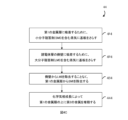
Classifications
-
- H—ELECTRICITY
- H10—SEMICONDUCTOR DEVICES; ELECTRIC SOLID-STATE DEVICES NOT OTHERWISE PROVIDED FOR
- H10P—GENERIC PROCESSES OR APPARATUS FOR THE MANUFACTURE OR TREATMENT OF DEVICES COVERED BY CLASS H10
- H10P70/00—Cleaning of wafers, substrates or parts of devices
- H10P70/20—Cleaning during device manufacture
- H10P70/27—Cleaning during device manufacture during, before or after processing of conductive materials, e.g. polysilicon or amorphous silicon layers
-
- H—ELECTRICITY
- H10—SEMICONDUCTOR DEVICES; ELECTRIC SOLID-STATE DEVICES NOT OTHERWISE PROVIDED FOR
- H10P—GENERIC PROCESSES OR APPARATUS FOR THE MANUFACTURE OR TREATMENT OF DEVICES COVERED BY CLASS H10
- H10P14/00—Formation of materials, e.g. in the shape of layers or pillars
- H10P14/60—Formation of materials, e.g. in the shape of layers or pillars of insulating materials
- H10P14/63—Formation of materials, e.g. in the shape of layers or pillars of insulating materials characterised by the formation processes
- H10P14/6326—Deposition processes
- H10P14/6328—Deposition from the gas or vapour phase
- H10P14/6334—Deposition from the gas or vapour phase using decomposition or reaction of gaseous or vapour phase compounds, i.e. chemical vapour deposition
- H10P14/6339—Deposition from the gas or vapour phase using decomposition or reaction of gaseous or vapour phase compounds, i.e. chemical vapour deposition deposition by cyclic CVD, e.g. ALD, ALE or pulsed CVD
-
- H—ELECTRICITY
- H10—SEMICONDUCTOR DEVICES; ELECTRIC SOLID-STATE DEVICES NOT OTHERWISE PROVIDED FOR
- H10P—GENERIC PROCESSES OR APPARATUS FOR THE MANUFACTURE OR TREATMENT OF DEVICES COVERED BY CLASS H10
- H10P14/00—Formation of materials, e.g. in the shape of layers or pillars
- H10P14/40—Formation of materials, e.g. in the shape of layers or pillars of conductive or resistive materials
- H10P14/42—Formation of materials, e.g. in the shape of layers or pillars of conductive or resistive materials using a gas or vapour
- H10P14/43—Chemical deposition, e.g. chemical vapour deposition [CVD]
- H10P14/432—Chemical deposition, e.g. chemical vapour deposition [CVD] using selective deposition
-
- H—ELECTRICITY
- H10—SEMICONDUCTOR DEVICES; ELECTRIC SOLID-STATE DEVICES NOT OTHERWISE PROVIDED FOR
- H10W—GENERIC PACKAGES, INTERCONNECTIONS, CONNECTORS OR OTHER CONSTRUCTIONAL DETAILS OF DEVICES COVERED BY CLASS H10
- H10W20/00—Interconnections in chips, wafers or substrates
- H10W20/01—Manufacture or treatment
- H10W20/031—Manufacture or treatment of conductive parts of the interconnections
- H10W20/056—Manufacture or treatment of conductive parts of the interconnections by filling conductive material into holes, grooves or trenches
- H10W20/057—Manufacture or treatment of conductive parts of the interconnections by filling conductive material into holes, grooves or trenches by selectively depositing, e.g. by using selective CVD or plating
-
- H—ELECTRICITY
- H10—SEMICONDUCTOR DEVICES; ELECTRIC SOLID-STATE DEVICES NOT OTHERWISE PROVIDED FOR
- H10P—GENERIC PROCESSES OR APPARATUS FOR THE MANUFACTURE OR TREATMENT OF DEVICES COVERED BY CLASS H10
- H10P14/00—Formation of materials, e.g. in the shape of layers or pillars
- H10P14/40—Formation of materials, e.g. in the shape of layers or pillars of conductive or resistive materials
- H10P14/42—Formation of materials, e.g. in the shape of layers or pillars of conductive or resistive materials using a gas or vapour
- H10P14/43—Chemical deposition, e.g. chemical vapour deposition [CVD]
-
- H—ELECTRICITY
- H10—SEMICONDUCTOR DEVICES; ELECTRIC SOLID-STATE DEVICES NOT OTHERWISE PROVIDED FOR
- H10W—GENERIC PACKAGES, INTERCONNECTIONS, CONNECTORS OR OTHER CONSTRUCTIONAL DETAILS OF DEVICES COVERED BY CLASS H10
- H10W20/00—Interconnections in chips, wafers or substrates
- H10W20/01—Manufacture or treatment
- H10W20/071—Manufacture or treatment of dielectric parts thereof
- H10W20/074—Manufacture or treatment of dielectric parts thereof of dielectric parts comprising thin functional dielectric layers, e.g. dielectric etch-stop, barrier, capping or liner layers
- H10W20/076—Manufacture or treatment of dielectric parts thereof of dielectric parts comprising thin functional dielectric layers, e.g. dielectric etch-stop, barrier, capping or liner layers in via holes or trenches
- H10W20/0765—Manufacture or treatment of dielectric parts thereof of dielectric parts comprising thin functional dielectric layers, e.g. dielectric etch-stop, barrier, capping or liner layers in via holes or trenches the thin functional dielectric layers being temporary, e.g. sacrificial layers
-
- H—ELECTRICITY
- H10—SEMICONDUCTOR DEVICES; ELECTRIC SOLID-STATE DEVICES NOT OTHERWISE PROVIDED FOR
- H10W—GENERIC PACKAGES, INTERCONNECTIONS, CONNECTORS OR OTHER CONSTRUCTIONAL DETAILS OF DEVICES COVERED BY CLASS H10
- H10W20/00—Interconnections in chips, wafers or substrates
- H10W20/40—Interconnections external to wafers or substrates, e.g. back-end-of-line [BEOL] metallisations or vias connecting to gate electrodes
- H10W20/41—Interconnections external to wafers or substrates, e.g. back-end-of-line [BEOL] metallisations or vias connecting to gate electrodes characterised by their conductive parts
- H10W20/44—Conductive materials thereof
- H10W20/4403—Conductive materials thereof based on metals, e.g. alloys, metal silicides
- H10W20/4432—Conductive materials thereof based on metals, e.g. alloys, metal silicides the principal metal being a noble metal, e.g. gold
Landscapes
- Internal Circuitry In Semiconductor Integrated Circuit Devices (AREA)
- Electrodes Of Semiconductors (AREA)
- Chemical Vapour Deposition (AREA)
Applications Claiming Priority (5)
| Application Number | Priority Date | Filing Date | Title |
|---|---|---|---|
| US202263315062P | 2022-02-28 | 2022-02-28 | |
| US63/315,062 | 2022-02-28 | ||
| US18/156,142 | 2023-01-18 | ||
| US18/156,142 US12588435B2 (en) | 2022-02-28 | 2023-01-18 | Selective inhibition for selective metal deposition |
| PCT/US2023/063327 WO2023164685A1 (en) | 2022-02-28 | 2023-02-27 | Selective inhibition for selective metal deposition |
Publications (2)
| Publication Number | Publication Date |
|---|---|
| JP2025512235A true JP2025512235A (ja) | 2025-04-17 |
| JP2025512235A5 JP2025512235A5 (enExample) | 2026-01-21 |
Family
ID=87761179
Family Applications (1)
| Application Number | Title | Priority Date | Filing Date |
|---|---|---|---|
| JP2024549153A Pending JP2025512235A (ja) | 2022-02-28 | 2023-02-27 | 選択的金属堆積のための選択的阻害 |
Country Status (5)
| Country | Link |
|---|---|
| US (1) | US12588435B2 (enExample) |
| JP (1) | JP2025512235A (enExample) |
| KR (1) | KR20240157662A (enExample) |
| TW (1) | TW202348825A (enExample) |
| WO (1) | WO2023164685A1 (enExample) |
Families Citing this family (4)
| Publication number | Priority date | Publication date | Assignee | Title |
|---|---|---|---|---|
| US20240431025A1 (en) * | 2023-06-26 | 2024-12-26 | International Business Machines Corporation | Corrosion resistant single damascene interconnects |
| WO2025217071A1 (en) * | 2024-04-08 | 2025-10-16 | Lam Research Corporation | Isonitrile inhibitors in ald |
| CN118291951B (zh) * | 2024-04-08 | 2025-02-25 | 合肥安德科铭半导体科技有限公司 | 一种有机小分子抑制剂及其在薄膜沉积中的应用方法 |
| CN121865857A (zh) * | 2026-03-13 | 2026-04-14 | 上海稷以科技有限公司 | 一种间隙特征的填充方法 |
Family Cites Families (10)
| Publication number | Priority date | Publication date | Assignee | Title |
|---|---|---|---|---|
| US8242019B2 (en) | 2009-03-31 | 2012-08-14 | Tokyo Electron Limited | Selective deposition of metal-containing cap layers for semiconductor devices |
| KR102711644B1 (ko) | 2018-03-20 | 2024-09-27 | 도쿄엘렉트론가부시키가이샤 | 통합형 반도체 공정 모듈을 포함하는 자기 인식 및 보정 이종 플랫폼, 및 이를 사용하기 위한 방법 |
| KR102800886B1 (ko) | 2018-08-23 | 2025-04-29 | 에이에스엠 아이피 홀딩 비.브이. | 기판 처리 장치 및 방법 |
| JP2020056104A (ja) | 2018-10-02 | 2020-04-09 | エーエスエム アイピー ホールディング ビー.ブイ. | 選択的パッシベーションおよび選択的堆積 |
| KR102759932B1 (ko) * | 2018-10-10 | 2025-01-23 | 도쿄엘렉트론가부시키가이샤 | 반도체 소자의 함입형 형상부를 저-저항률 금속으로 충전하기 위한 방법 |
| US11282745B2 (en) | 2019-04-28 | 2022-03-22 | Applied Materials, Inc. | Methods for filling features with ruthenium |
| US20200347493A1 (en) | 2019-05-05 | 2020-11-05 | Applied Materials, Inc. | Reverse Selective Deposition |
| US11286556B2 (en) | 2020-04-14 | 2022-03-29 | Applied Materials, Inc. | Selective deposition of titanium films |
| US20230245924A1 (en) | 2020-06-23 | 2023-08-03 | Lam Research Corporation | Selective deposition using graphene as an inhibitor |
| US11094543B1 (en) | 2020-12-04 | 2021-08-17 | Tokyo Electron Limited | Defect correction on metal resists |
-
2023
- 2023-01-18 US US18/156,142 patent/US12588435B2/en active Active
- 2023-02-27 KR KR1020247028048A patent/KR20240157662A/ko active Pending
- 2023-02-27 JP JP2024549153A patent/JP2025512235A/ja active Pending
- 2023-02-27 WO PCT/US2023/063327 patent/WO2023164685A1/en not_active Ceased
- 2023-03-01 TW TW112107265A patent/TW202348825A/zh unknown
Also Published As
| Publication number | Publication date |
|---|---|
| WO2023164685A1 (en) | 2023-08-31 |
| TW202348825A (zh) | 2023-12-16 |
| US12588435B2 (en) | 2026-03-24 |
| US20230274932A1 (en) | 2023-08-31 |
| KR20240157662A (ko) | 2024-11-01 |
Similar Documents
| Publication | Publication Date | Title |
|---|---|---|
| US8178439B2 (en) | Surface cleaning and selective deposition of metal-containing cap layers for semiconductor devices | |
| US6605549B2 (en) | Method for improving nucleation and adhesion of CVD and ALD films deposited onto low-dielectric-constant dielectrics | |
| US6852635B2 (en) | Method for bottomless deposition of barrier layers in integrated circuit metallization schemes | |
| US7498242B2 (en) | Plasma pre-treating surfaces for atomic layer deposition | |
| US12588435B2 (en) | Selective inhibition for selective metal deposition | |
| US8173538B2 (en) | Method of selectively forming a conductive barrier layer by ALD | |
| TWI827553B (zh) | 用於內連線的釕金屬特徵部填補 | |
| TWI694501B (zh) | 防止銅擴散的介電/金屬阻障集成 | |
| US7709376B2 (en) | Method for fabricating semiconductor device and semiconductor device | |
| US20100248473A1 (en) | Selective deposition of metal-containing cap layers for semiconductor devices | |
| US7928006B2 (en) | Structure for a semiconductor device and a method of manufacturing the same | |
| CN110970394B (zh) | 半导体结构及用于半导体工艺的方法 | |
| US20240213093A1 (en) | Catalyst-enhanced chemical vapor deposition | |
| JP2006024668A (ja) | 半導体装置の製造方法 | |
| US20250376762A1 (en) | Cyclic plasma and thermal process to improve pecvd ti silicide deposition selectivity | |
| KR100891524B1 (ko) | 반도체 소자의 제조방법 | |
| TW202527060A (zh) | 介層窗填充方法 | |
| CN119998487A (zh) | 使用苯胺钝化的介电质上介电质选择性沉积 | |
| JP2006147895A (ja) | 半導体装置の製造方法 |
Legal Events
| Date | Code | Title | Description |
|---|---|---|---|
| A521 | Request for written amendment filed |
Free format text: JAPANESE INTERMEDIATE CODE: A523 Effective date: 20260108 |
|
| A621 | Written request for application examination |
Free format text: JAPANESE INTERMEDIATE CODE: A621 Effective date: 20260108 |